advanced channel engineering achieving aggressive ...dec 07, 2011 · 26 summary • deeply...
TRANSCRIPT
1
Advanced Channel Engineering Achieving Aggressive Reduction of
VT Variation for Ultra-Low-Power Applications
K.Fujita, Y.Torii, M.Hori, J.Oh, L.Shifren*, P.Ranade*, M.Nakagawa, K.Okabe, T.Miyake, K.Ohkoshi, M.Kuramae,
T.Mori, T.Tsuruta, S.Thompson*, T.Ema
Fujitsu Semiconductor Ltd. *SuVolta Inc.
2
Outline• Introduction• Transistor Structure• Features of Process Flow and
Verification• 65nm 6T-SRAM Evaluation Results• Summary
3
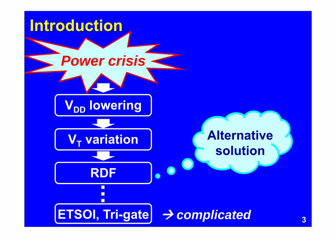
Introduction
complicated
Power crisis
VDD lowering
VT variation
RDF
ETSOI, Tri-gate
Alternative solution
4
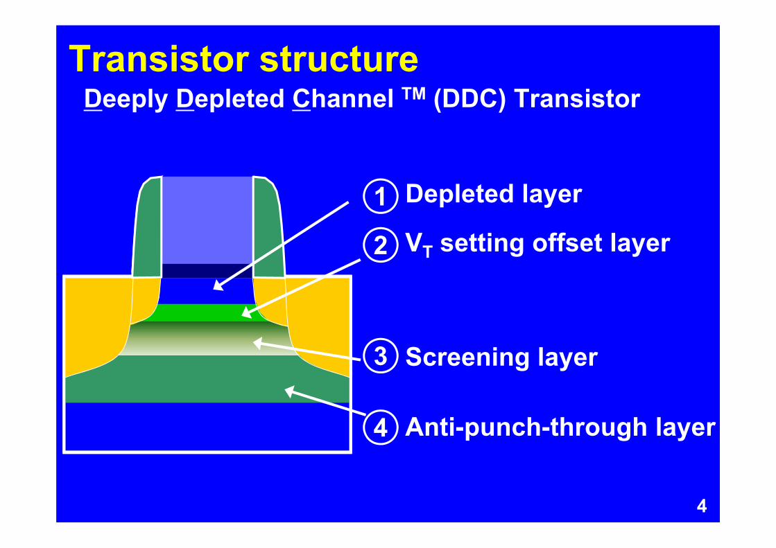
Transistor structureDeeply Depleted Channel TM (DDC) Transistor
1
2
3
4
Depleted layer
VT setting offset layer
Screening layer
Anti-punch-through layer
5
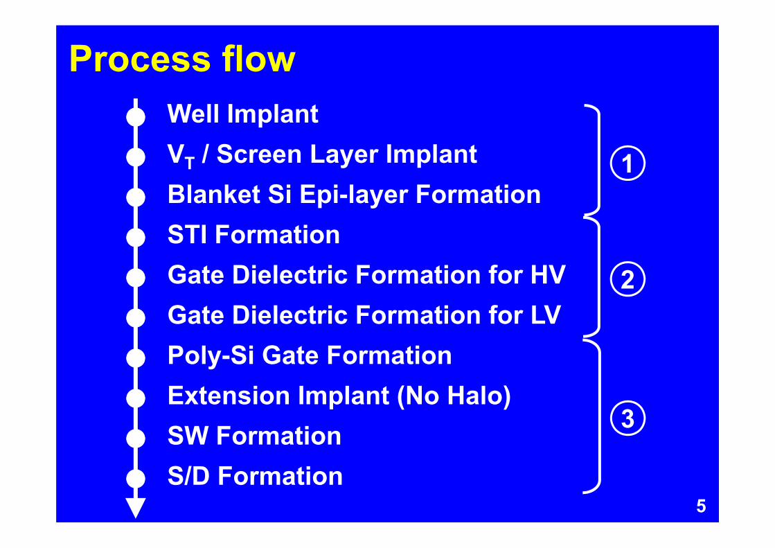
Process flowWell ImplantVT / Screen Layer ImplantBlanket Si Epi-layer FormationSTI FormationGate Dielectric Formation for HVGate Dielectric Formation for LVPoly-Si Gate FormationExtension Implant (No Halo)SW FormationS/D Formation
1
2
3
6
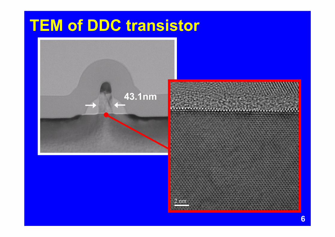
TEM of DDC transistor
43.1nm
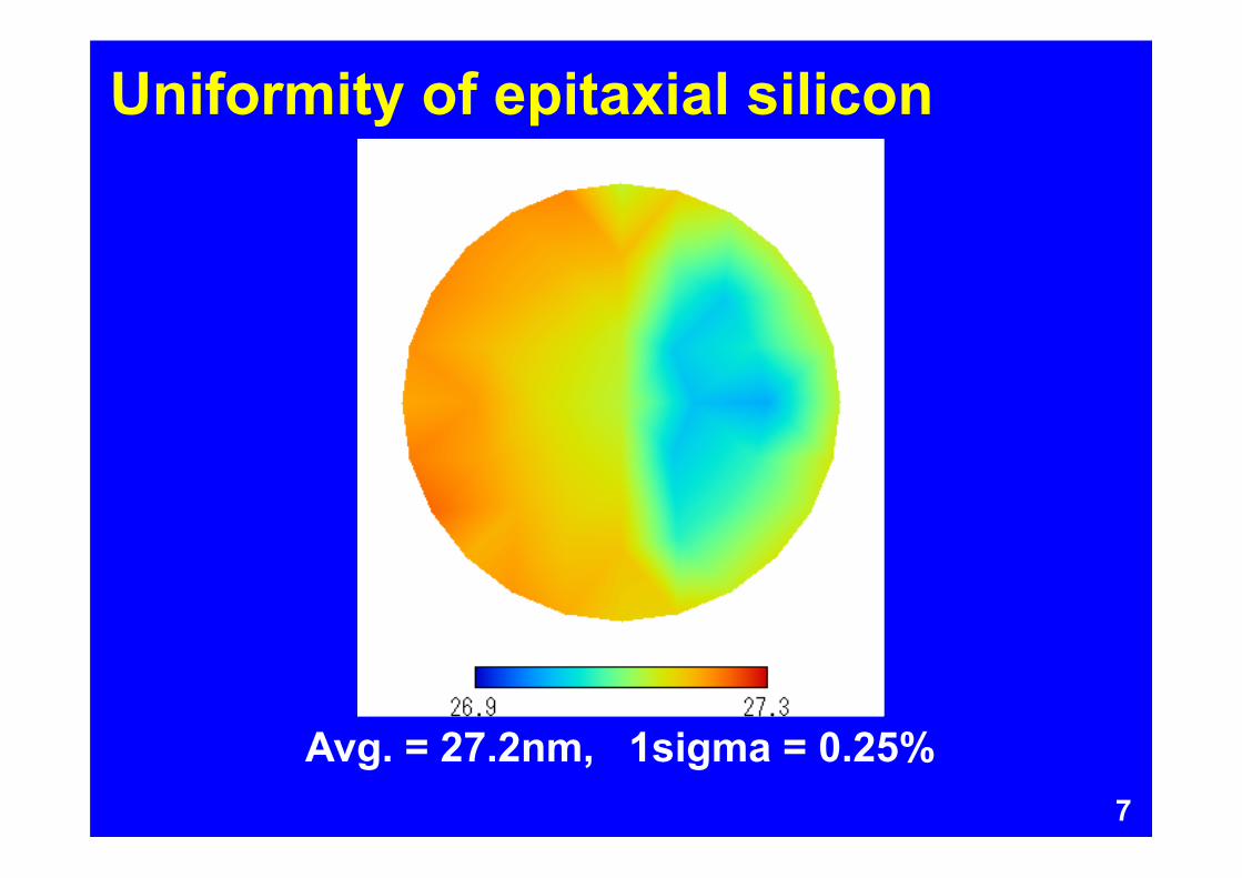
Uniformity of epitaxial silicon
7
Avg. = 27.2nm, 1sigma = 0.25%
8
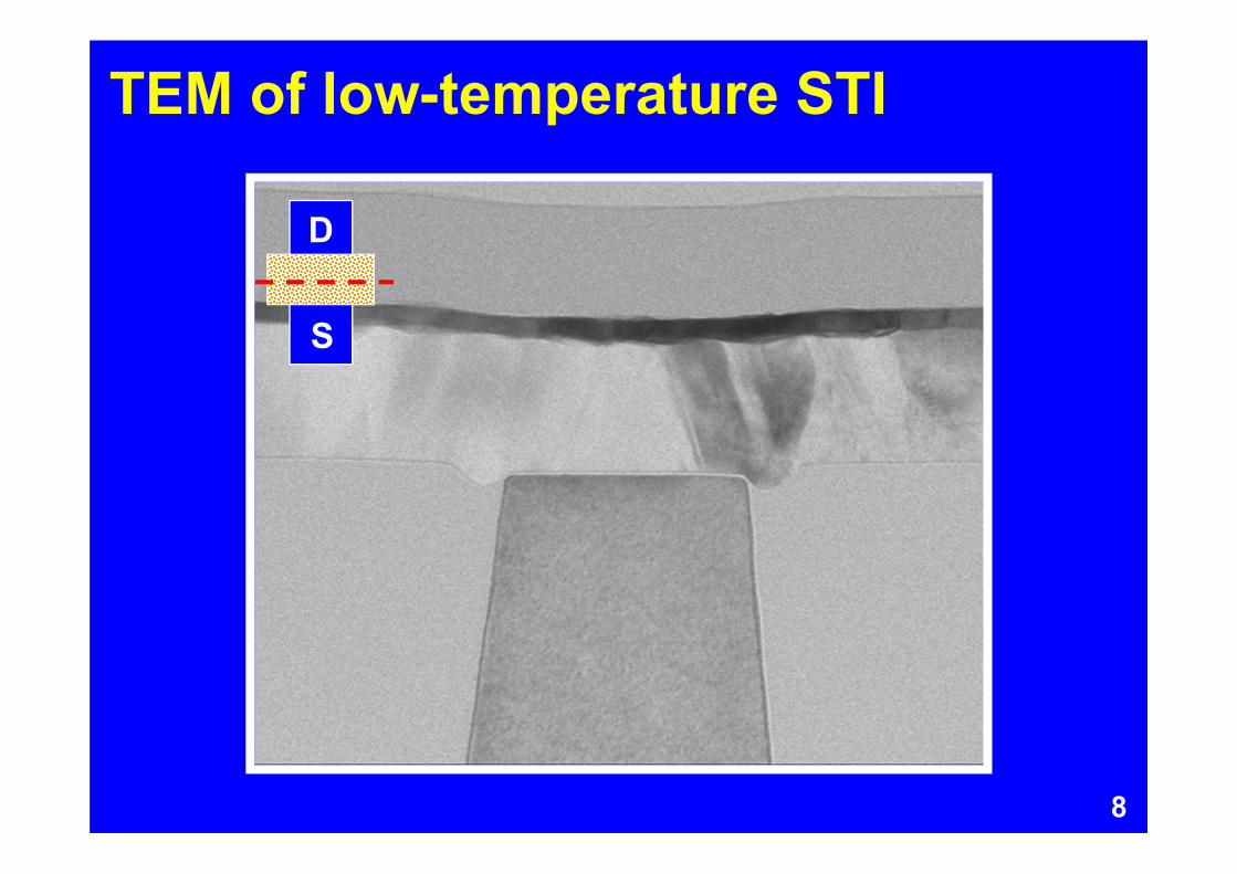
TEM of low-temperature STI
S
D
9
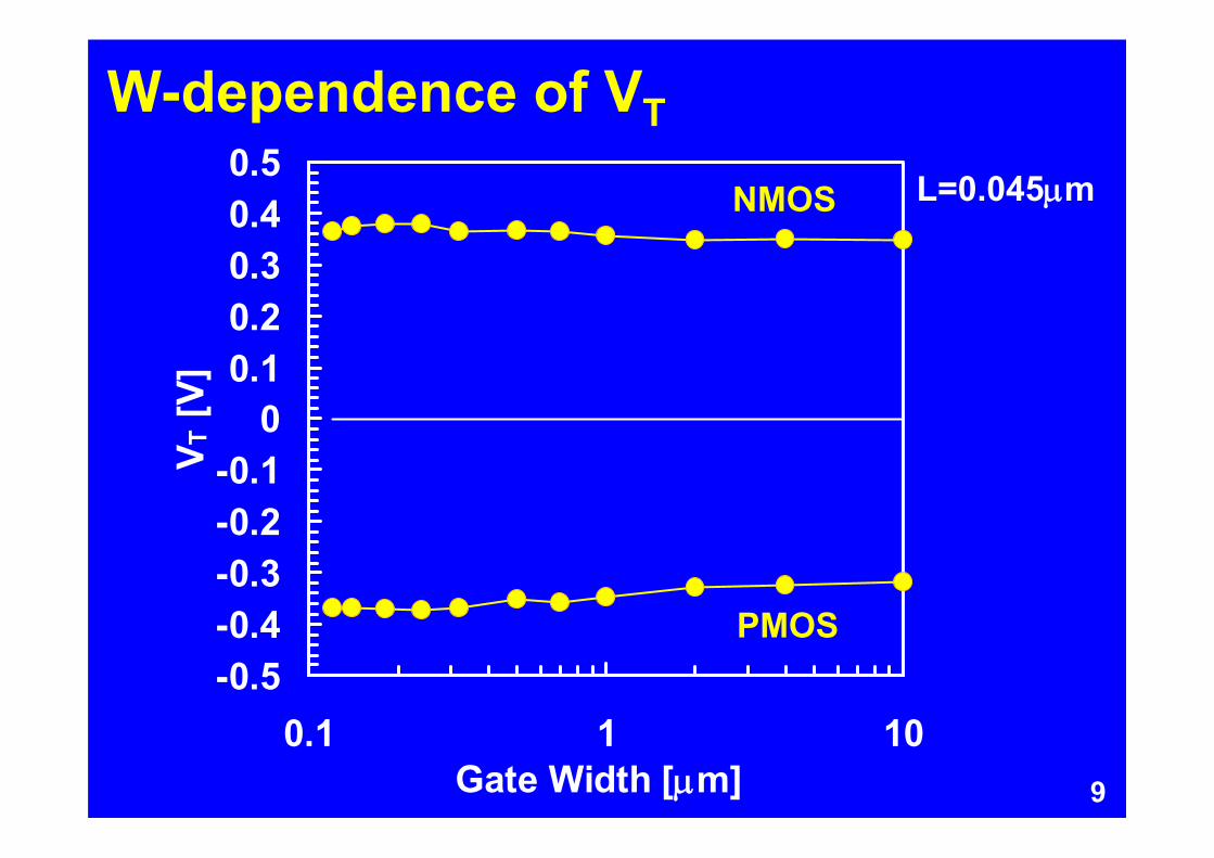
-0.5-0.4-0.3-0.2-0.1
00.10.20.30.40.5
0.1 1 10Gate Width [m]
V T [V
]
W-dependence of VT
NMOS
PMOS
L=0.045m
10
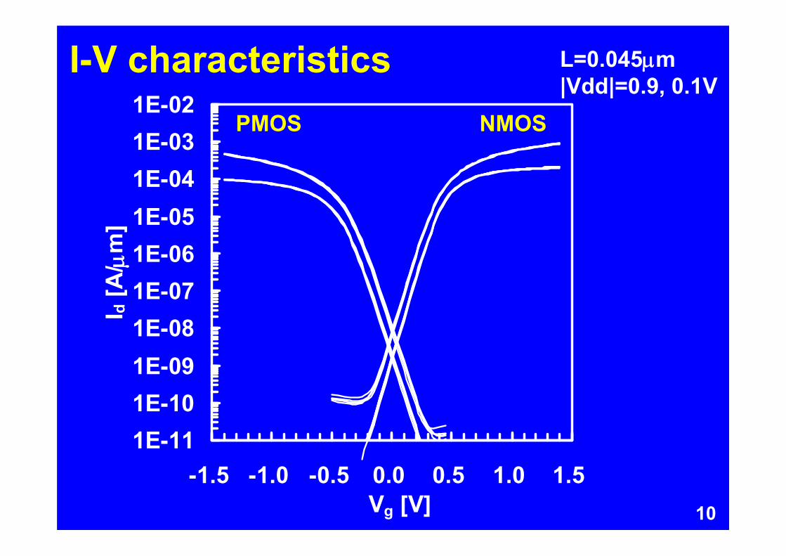
NMOSPMOS
I-V characteristics L=0.045m|Vdd|=0.9, 0.1V
1E-111E-101E-091E-081E-071E-061E-051E-041E-031E-02
-1.5 -1.0 -0.5 0.0 0.5 1.0 1.5Vg [V]
I d [A
/ m
]
Summary of STI
11
• Excellent STI profile• No anomalous W dependence• Nice sub-threshold characteristics
No concern about low temp. STI
12
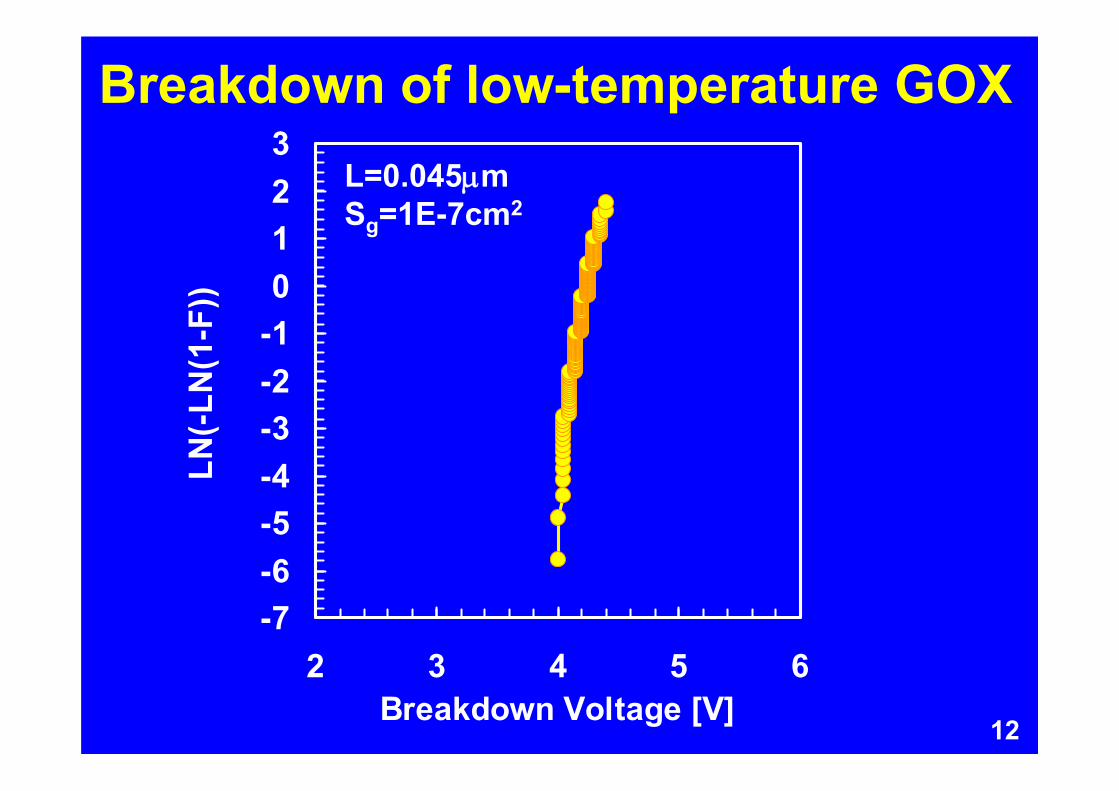
Breakdown of low-temperature GOX
-7-6-5-4-3-2-10123
2 3 4 5 6Breakdown Voltage [V]
LN(-L
N(1
-F))
L=0.045mSg=1E-7cm2
13
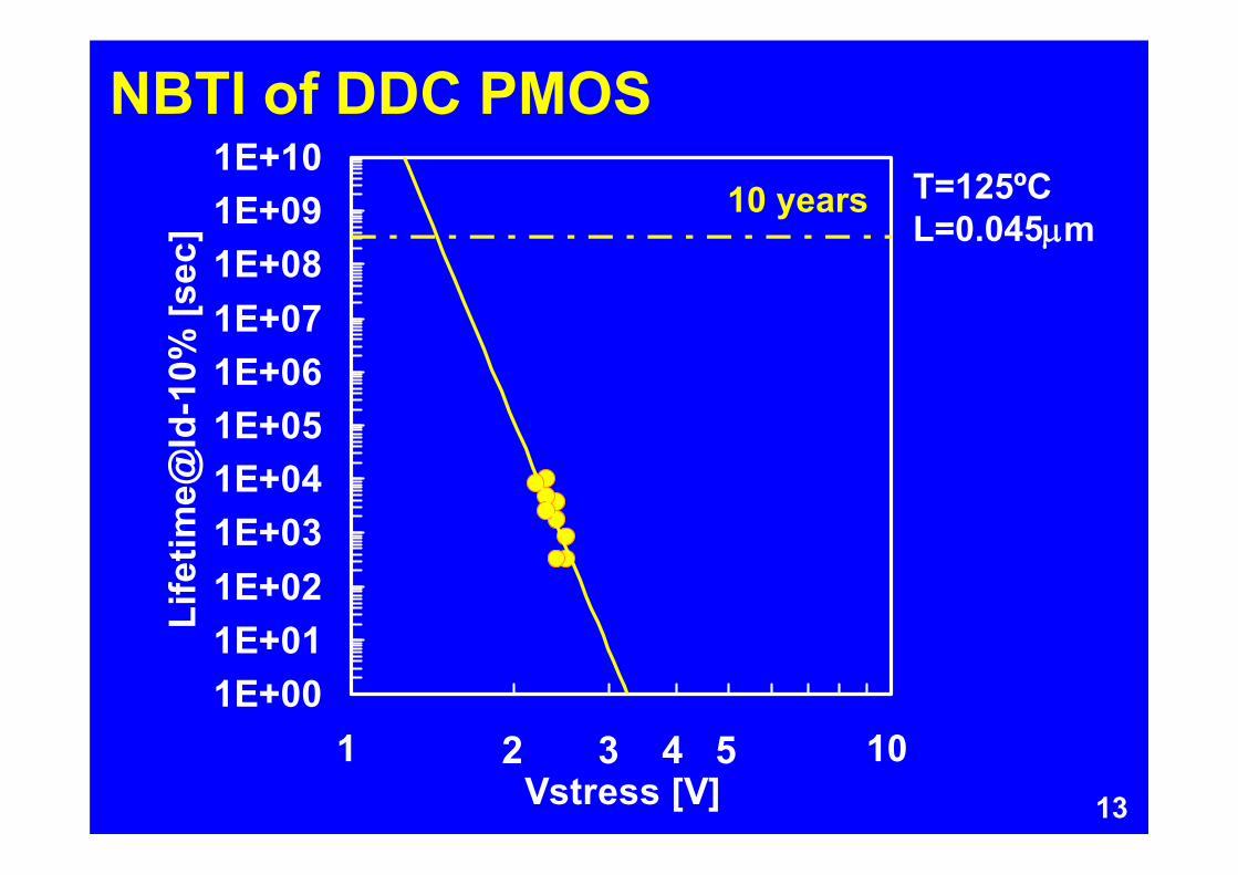
NBTI of DDC PMOS10 years
1E+001E+011E+021E+031E+041E+051E+061E+071E+081E+091E+10
1 10 Vstress [V]
Life
time@
Id-1
0% [s
ec]
2 3 4 5
T=125ºCL=0.045m
14
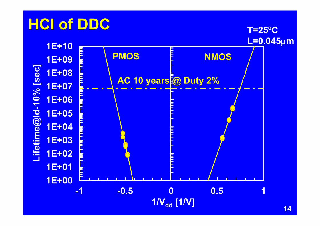
HCI of DDC
1E+001E+011E+021E+031E+041E+051E+061E+071E+081E+091E+10
Life
time@
Id-1
0% [s
ec]
1/Vdd [1/V]-1 10-0.5 0.5
AC 10 years @ Duty 2%
NMOSPMOS
T=25ºCL=0.045m
15
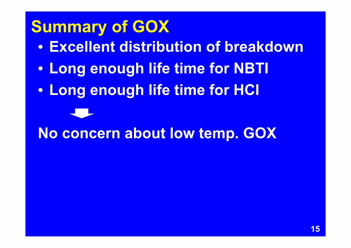
Summary of GOX• Excellent distribution of breakdown• Long enough life time for NBTI• Long enough life time for HCI
No concern about low temp. GOX
16
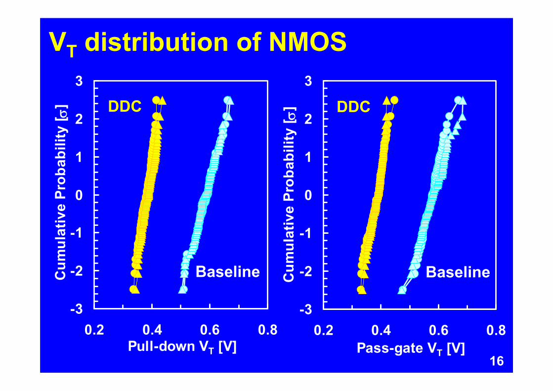
VT distribution of NMOS
-3
-2
-1
0
1
2
3
0.2 0.4 0.6 0.8Pull-down VT [V]
Cum
ulat
ive
Prob
abili
ty [
]
-3
-2
-1
0
1
2
3
0.2 0.4 0.6 0.8Pass-gate VT [V]
Cum
ulat
ive
Prob
abili
ty [
]Baseline Baseline
DDC DDC

17
VT distribution of PMOS
-3
-2
-1
0
1
2
3
-0.8-0.6-0.4-0.2Pull-up VT [V]
Cum
ulat
ive
Prob
abili
ty [
] , Baseline, DDC
18
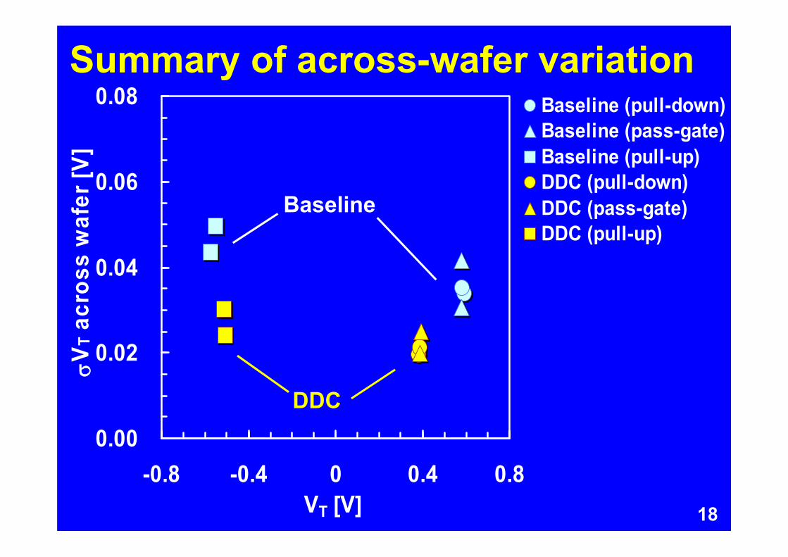
0.00
0.02
0.04
0.06
0.08
-0.8 -0.4 0 0.4 0.8VT [V]
V T
acr
oss
waf
er [V
]Baseline (pull-down)Baseline (pass-gate)Baseline (pull-up)DDC (pull-down)DDC (pass-gate)DDC (pull-up)
Summary of across-wafer variation
Baseline
DDC

19
-3
-2
-1
0
1
2
3
-0.2 -0.1 0 0.1 0.2Pass-gate VT [V]
Cum
ulat
ive
Prob
abili
ty [
]-3
-2
-1
0
1
2
3
-0.2 -0.1 0 0.1 0.2Pull-down VT [V]
Cum
ulat
ive
Prob
abili
ty [
]VT matching of NMOS
BaselineDDC
BaselineDDC
20
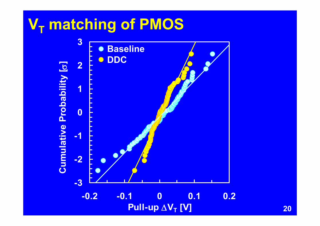
VT matching of PMOS
-3
-2
-1
0
1
2
3
-0.2 -0.1 0 0.1 0.2Pull-up VT [V]
Cum
ulat
ive
Prob
abili
ty [
]BaselineDDC

21
Summary of VT matching
Baseline
DDC
0.00
0.02
0.04
0.06
0.08
-0.8 -0.4 0 0.4 0.8VT [V]
V T /
SQR
T(2)
[V]
Baseline (pull-down)Baseline (pass-gate)Baseline (pull-up)DDC (pull-down)DDC (pass-gate)DDC (pull-up)
22
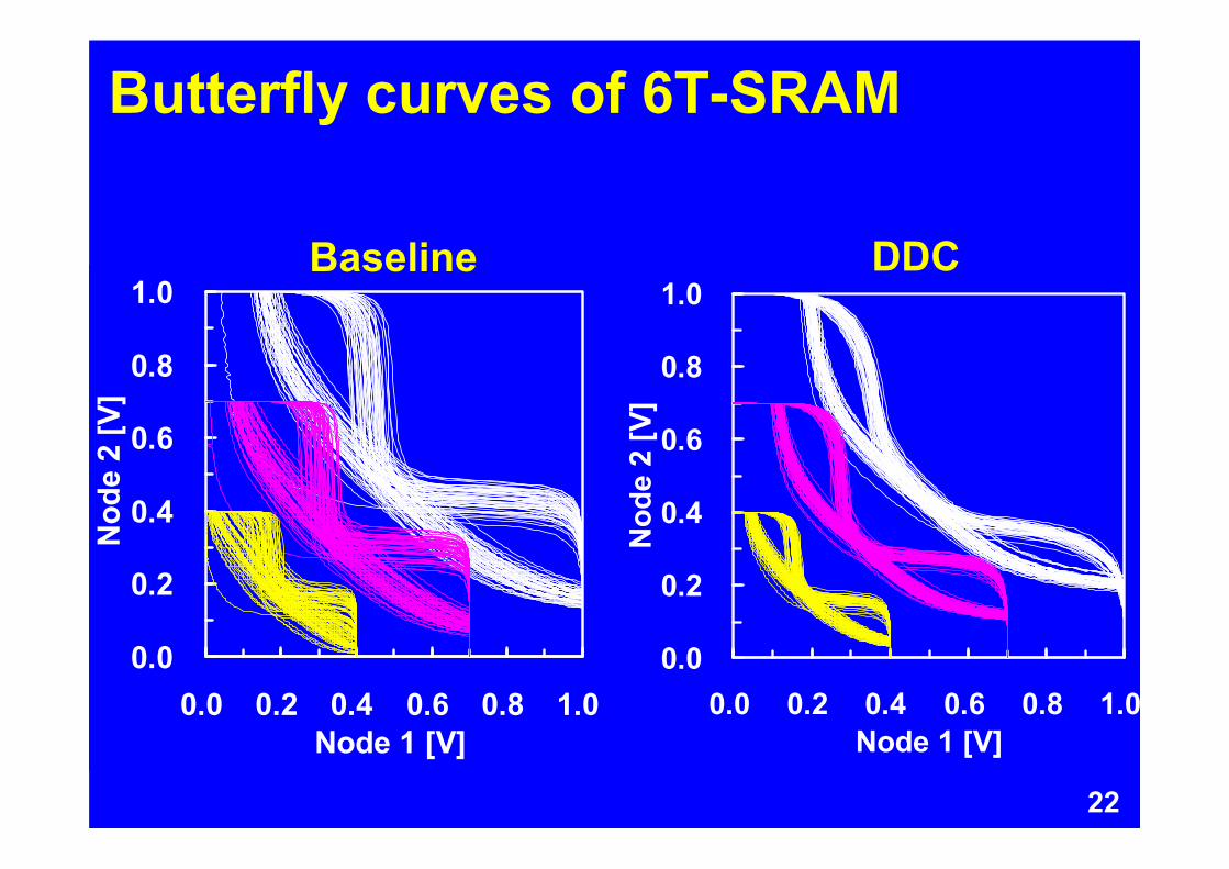
0.0
0.2
0.4
0.6
0.8
1.0
0.0 0.2 0.4 0.6 0.8 1.0Node 1 [V]
Nod
e 2
[V]
0.0
0.2
0.4
0.6
0.8
1.0
0.0 0.2 0.4 0.6 0.8 1.0Node 1 [V]
Nod
e 2
[V]
Butterfly curves of 6T-SRAM
Baseline DDC
23
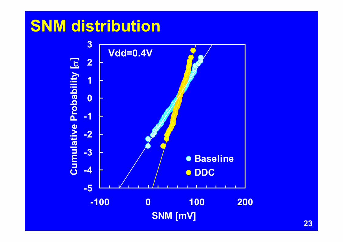
SNM distribution
-5
-4
-3
-2
-1
0
1
2
3
-100 0 100 200SNM [mV]
Cum
ulat
ive
Prob
abili
ty [
]
BaselineDDC
Vdd=0.4V

24
Vdd dependence of SNM
0123456789
10
0.0 0.2 0.4 0.6 0.8 1.0Vdd [V]
SNM
(mea
n/1σ
) [σ]
BaselineDDC
25
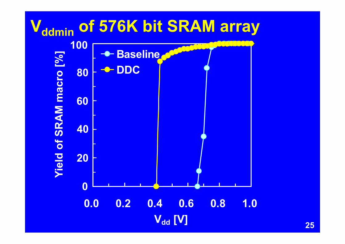
Vddmin of 576K bit SRAM array
0.0 0.2 0.4 0.6 0.8 1.0Vdd [V]
BaselineDDC
100
80
60
40
20
0
Yiel
d of
SR
AM
mac
ro [%
]
26
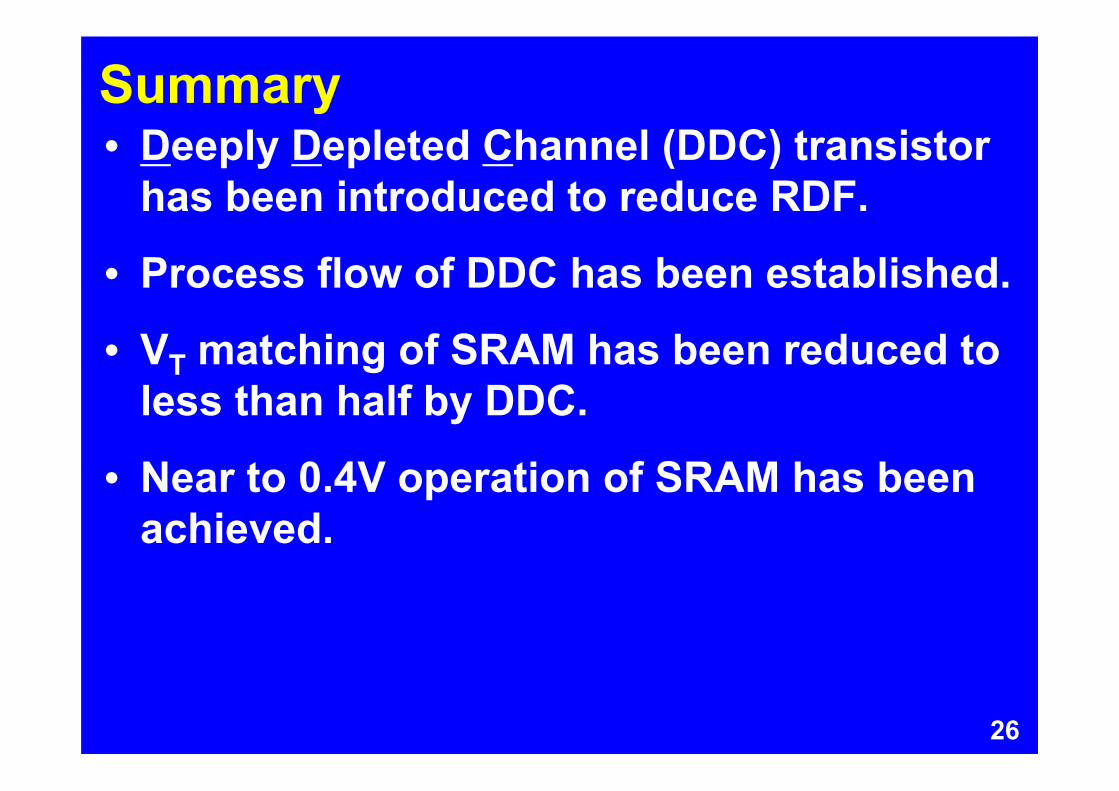
Summary• Deeply Depleted Channel (DDC) transistor
has been introduced to reduce RDF.
• Process flow of DDC has been established.
• VT matching of SRAM has been reduced to less than half by DDC.
• Near to 0.4V operation of SRAM has been achieved.