advanced circuits and systems for rf, mmw and thz wireless
TRANSCRIPT

STMicroelectronics and Université de Lille 1
Advanced circuits and systems for RF, mmW and THz wireless
communications– HDR thesis Thèse HDR: Conception de circuits et systèmes avancés
pour des applications de communications sans fil en gamme RF, mmW et THz
Andreia Cathelin Nitescu-Henry
May 6, 2013

Advanced circuits and systems for RF, mmW and THz wireless communications– HDR thesis
Andreia Cathelin May 2013 Page 3
ACKNOWLEDGEMENTS
I would first like to show my gratitude to professor Andreas Kaiser from IEMN, promoter of this
work. Andreas has been first my microelectronics professor at ISEN, then my PhD advisor and finally
road companion for a large majority of research activity developed jointly during the last 15 years, in
the frame of the common laboratory ST-IEMN. And, of course, a great friend!
Several other professors have been involved in most of the joint collaborative research. I warmly
thank them for the great research that we lead together in a very productive and friendly atmosphere;
they are, in order of appearance: François Danneville from IEMN Lille, Jean-Baptiste Begueret and
Eric Kerhervé from IMS Bordeaux, Eric Tournier and Olivier Llopis from LAAS Toulouse, Christian
Person from Lab-Stic Brest, Nathalie Rolland from IEMN, Ali Niknejad from UC Berkeley, Ullrich
Pfeiffer from University of Wuppertal, Bram Nauta from University of Twente, Jan Rabaey and Bora
Nikolic from UC Berkeley.
Our former PhD students have boldly followed us and then found their own way, always hard
working and with good humor. I as well warmly thank them for the nice cooperation we had: David
Chamla, Stéphane Razafimandimby, Cyril Tilhac, Baudouin Martineau, Nicolas Seller, Jean Gorisse,
Yenny Pinto, Romain Crunelle, Jonathan Muller, Mathieu Egot, Fawzi Houfaf, Hani Sherry; as well as
those still on the way: David Borggreve, Camilo Salazar, and Dajana Danilovic.
During all these years I have been empowered by the management of STMicroelectronics in Crolles,
who has created the perfect environment for advanced R&D inside the company. I would like to
address my gratitude to Philippe Magarshack, Executive VP of ST, and Dr. Pierre Dautriche, Director,
who have shown their trust to my research activity and are supporting it.
I am extremely grateful to the members of this habilitation jury. Professors Bram Nauta from
University of Twente, Jan Rabaey from UC Berkeley and Paul-Alain Rolland from University of Lille
have kindly accepted to report on this work. As well, thank you to the members of the jury: Dr. Pierre
Dautriche from STMicroelectronics, professor Raymond Quéré from XLIM Limoges and professor
Alain Cappy from IEMN. Thank you as well Alain for your trust and support during all these years of
common lab!
I would like to cite as well several colleagues from STMicroelectronics who are wonderful
companions on the R&D path: Didier Belot, Frédéric Paillardet, Olivier Richard, Frédéric Gianesello,
Stéphane Le Tual, Pratap Narayan Singh, Frédéric Hasbani, Philippe Flatresse, Christophe Garnier,
Pierre Busson, Caroline Arnaud, Patrick Cogez as well as Pascale Maillet-Contoz and Nicolas
Rolland; also former colleagues: Danilo Gerna, Carlo Tinella and Franck Badets. I would not be able
to finish this list without naming four gentlemen now retired from ST who have taught me the
dedicated and patient way of doing advanced R&D in industry: Ernesto Perea, Marcel Roche, Eugène
Mackowiak and Jean-Pierre Schoellkopf.
Last but not least, I would like to thank all my family for their support, with patience and lots of love
and humor.
à Philippe et aux enfants, Emilie et Mircea

Advanced circuits and systems for RF, mmW and THz wireless communications– HDR thesis
Andreia Cathelin May 2013 Page 5
Soyons comme le chevalier Bayard: sans peur et sans reproches….
à Laval dans le Grésivaudan, le 6 mai 2013

Advanced circuits and systems for RF, mmW and THz wireless communications– HDR thesis
Andreia Cathelin May 2013 Page 7
TABLE OF CONTENTS
I. General Introduction ................................................................................................................... 9
II. Analog integrated continuous time filters for wireless applications .................................. 11
II.1 Preamble .............................................................................................................................. 11
II.2 Reconfigurable filters for cellular applications .............................................................. 12
II.3 Filter tuning methodology for reconfigurable architectures ....................................... 23
II.4 Reconfigurable Gm-C filters with record cut-off frequency up to 10GHz ................ 36
II.5 Conclusions and perspectives .......................................................................................... 41
III. BAW-IC co-integration for RF circuits ................................................................................ 43
III.1 Preamble .............................................................................................................................. 43
III.2 BAW technology ................................................................................................................ 44
III.3 BAW resonator filters ........................................................................................................ 47
III.4 Tunable BAW filters ............................................................................................................ 51
III.5 Tuning circuitry for BAW filters ...................................................................................... 58
III.6 Other co-integrated circuits using BAW devices: oscillators, phase noise integrated
test-bench ........................................................................................................................................ 66
III.7 Conclusions and perspectives .......................................................................................... 76
IV. mmW and THz design in deep submicron CMOS technologies .................................... 77
IV.1 Preamble .............................................................................................................................. 77
IV.2 Target applications in the mmW band ............................................................................ 78
IV.3 Building a robust design methodology for mmW circuits in deep submicron CMOS
81
IV.4 Towards complex circuits and systems for mmW applications .................................. 94
IV.5 Conclusions and perspectives ........................................................................................ 128
V. General Conclusion and perspectives ................................................................................... 129
VI. Extended Curriculum Vitae ................................................................................................ 131
VI.1 Curriculum Vitae ............................................................................................................. 131
VI.2 Membership in conferences, reviewer, awards ........................................................... 134
VI.3 M.S. students supervision through industrial internship .......................................... 135
VI.4 Ph.D. students supervision (my supervision quota in bold blue) ................................... 136
VI.5 Participation to Ph.D. defense juries ............................................................................. 140
VI.6 Teaching activities (see also Invited talks in workshops/ seminars/ tutorials)................. 142

Advanced circuits and systems for RF, mmW and THz wireless communications– HDR thesis
Andreia Cathelin May 2013 Page 8
VI.7 Collaborative projects ...................................................................................................... 143
VI.8 Public Patents (as per Google Patents, on July 30, 2012) ............................................ 144
VI.9 Publications in peer-reviewed journals ........................................................................ 147
VI.10 Publications in peer-reviewed conferences with proceedings .............................. 149
VI.11 Invited talks in conferences with proceedings ......................................................... 156
VI.12 Invited talks in workshops/ seminars/ tutorials .................................................... 157
VI.13 Book chapters ................................................................................................................ 158
VI.14 Workshop/ Seminar/ Short courses as organizer .................................................. 159

Advanced circuits and systems for RF, mmW and THz wireless communications– HDR thesis
Andreia Cathelin May 2013 Page 9
I. GENERAL INTRODUCTION
This Habilitation Thesis manuscript presents some major results of the applied R&D work
that I have conducted at STMicroelectronics since beginning of year 2000, and within a close
collaboration with IEMN Lille. This research work has been supported by the numerous
Cifre PhD thesis that I have been supervising as industrial advisor, the academic part being
performed in most of the cases by Doctor Andreas Kaiser, Directeur de Recherche CNRS at
IEMN. For several subjects, we have put in place a second academic supervision, like for
example with UC Berkeley in California – professor Ali Niknejad, University of Twente in
the Netherlands – professor Bram Nauta and University of Wuppertal – professor Ullrich
Pfeiffer.
The first big theme of my scientific research is focused on the design of integrated circuits
and systems for wireless applications in the RF frequency bands.
The first part is dedicated to the integration of continuous-time filtering solutions for 2-, 3-
and 4G mobile communications, work carried out in the early 2000 years. Given the large
variety of standards to be addressed in the mobile terminals, it has come out as an
interesting research topic to address analog base-band filtering solutions which are flexible
and reconfigurable in terms of band pass, order, linearity and noise. Hence, several
integrated circuits have been proposed using the Gm-C filtering technique, showing
flexibility for GSM to W-CDMA standards requirements, in (Bi)CMOS 0.25 and 0.13µm. This
kind of analog continuous time filters has been pushed to its utmost limit (CMOS 65nm), as
we have then demonstrated its operation up to a record cut-of frequency of 10GHz. A
systematic approach for the cut-off frequency tuning of such filters has been proposed as
well as demonstrated experimentally.
In a second part, this document presents the results of the research carried out on the
potentialities of co-integration between BAW (Bulk Acoustic Wave) and Silicon traditional
technologies, around year 2005. New perspectives in terms of circuits and systems have been
opened for applications in the frequency bands below 10GHz. In the frame of a W-CDMA
receiver, an innovative solution has been proposed for the replacement of external SAW
filters with miniaturized co-integrated BAW-IC RF filters showing also electronically tuning
capabilities. On a system level, in collaboration with LAAS in Toulouse, we have proposed a
novel solution of fully integrated test-bench for phase noise measurements, based also on a
co-integration between BAW and traditional IC technology. When used in a communication
system, this integrated test-bench permits to dynamically adjust the system performance
and hence power consumption, as a function of the environmental and ageing conditions.
This concept represents an early implementation of the principle “Sense and React” which
appears since only few years in most of the mobile communication systems showing low
power features.

Advanced circuits and systems for RF, mmW and THz wireless communications– HDR thesis
Andreia Cathelin May 2013 Page 10
The second big theme addressed by my research brings solutions for the design of
communication systems in the millimeter wave band, and at the end bringing an opening to
THz imaging.
The interest for high data-rate (Gb/s) wireless communications in the 60GHz frequency
band and using fully integrated Silicon technologies has appeared middle of last decade. I
have hence put in place a research activity in order to bring to life an industrially robust
design methodology for millimeter wave systems using advanced (Bi)CMOS technologies.
This expertise has then been used by an industrial design team from ST and CEA-Leti, to
which I have participated, in order to propose one of the first fully integrated CMOS 65nm
WirelessHD transceiver modules with integrated antenna and millimeter wave packaging
solution. I have then conducted new research topics in order to propose alternative system
architectures for such high data-rate applications, either in order to add more flexibility in
the operation mode or to increase the energy efficiency towards mobile application use-
cases. Novel massively digital software defined radio transmitter architecture has been
proposed for these Gb/s communications. In the same time, an alternative Local Oscillator
based beam-forming solution has been studied, relying on Coupled Oscillators Array with
Injection Locking capability.
Finally, during the last few years, jointly lead with University of Wuppertal and IEMN, we
have proposed fully integrated state of the art solutions for THz imaging using regular
CMOS technology. For the very first time ever, a 65nm CMOS 1 k-pixel fully integrated
camera has been proposed, able to detect and format signals in the frequency band from 650
to 1000GHz. The principle of self-mixing in the channel of a FET transistor is used to provide
the detection of the THz signals. This major innovation in the field of integrated solutions for
THz imaging opens new door for creating markets of miniaturized products for: detecting
hidden metallic objects, monitoring the moisture level in the agriculture industry, non-
destructive non-harmful imaging or spectroscopy in the biological domain and much more.
Recently, this work has been acknowledged by the international scientific community with
the 2012 STMicrolectronics Technology Council Innovation Prize and the 2013 ISSCC Jan
Van Vessem Award for Outstanding European Paper. Since July 2012, the Imaging Division
of STMicroelectronics has added the Silicon integrated THz technology to its product road-
map.
All this work is presented in the three major chapters of this thesis. Each research topic has
its own preamble, and conclusions and perspectives section. A large part of the technical
details given in this manuscript are drawn from the major publications I have co-authored,
such as JSSC or ISSCC papers.

Advanced circuits and systems for RF, mmW and THz wireless communications– HDR thesis
Andreia Cathelin May 2013 Page 11
II. ANALOG INTEGRATED CONTINUOUS TIME FILTERS FOR
WIRELESS APPLICATIONS
II.1 PREAMBLE
Early 2000, all around the world, all the major academic and industrial parties focused a
large part of their research on multi-mode communication system for cellular applications.
The 2, 3 and yet to come 4G standards had to co-exist, and hence a lot of research has started
on reconfiguration ability of wireless transceivers. As well, it was the ending age of BiCMOS
wireless transceivers and the opening era for the industrial full CMOS solutions. Under
these circumstances, at STMicroelectronics we have as well decided to work on re-
configurable transceivers for applications such as GSM, DCS, W-CDMA. Inside this frame, I
have started a research activity concerning the re-configurable analog integrated continuous
time filters for such cellular applications, and we arrived under short time to the need for
flexible and reconfigurable solutions.
The research presented in this section has been carried out at STMicroelectronics with two
trainee Master students, Laurent Fabre and Laurent Baud, in 2001 and respectively 2002, and
was followed by a thorough research performed in collaboration with IEMN/ISEN,
professor Andreas Kaiser, in the frame of the Cifre Ph.D. thesis of David Chamla, from 2002
to the end of 2005. The targeted applications were GSM to W-CDMA, with cut-off
frequencies in the range of hundred of kHz up to few MHz.
After a break of several years, we have decided to extend these analog filtering methods to
very wide band applications for Gb/s data rate communications, such as IEEE 802. 15.3.c
(Wi-HDMI or WiGig) for the wireless part, and high data rate optical wireline
communications. In 2008-9 this research has been done internally at STMicroelectronics in
collaboration with Romain Ferragut (cut-off frequency brought up to 1GHz). It was then
continued after 2009 by a Cifre Ph.D. thesis, student Fawzi Houfaf, in collaboration with the
University of Twente, professor Bram Nauta and IEMN/ISEN, professor Andreas Kaiser.
This last topic brought us to the world record cut-off frequency of 10GHz ever attained for
an analog continuous time low pass filter, published early 2012 at ISSCC.

Advanced circuits and systems for RF, mmW and THz wireless communications– HDR thesis
Andreia Cathelin May 2013 Page 12
II.2 RECONFIGURABLE FILTERS FOR CELLULAR APPLICATIONS
The research presented in this section addresses the analog base-band section of a zero-IF
architecture receiver, which was considered the best choice for such re-configurable cellular
systems (see Figure II-1). We focus on the low-pass filter.
Figure II-1 Zero-IF receiver considered in this work
When considering the major mobile communications standard for cellular, we rapidly can
state the need for a wide tuning capability in the analog base-band filtering section. The
table bellow illustrates this fact.
Table II-1 Major cellular standards bandwidth specifications
System level research has determined the specifications needed for a reconfigurable analog
base-band low-pass filter section, when considering several mobile applications
specifications. These values are given in Table II-2, and they consist in the starting point for
the research presented in this section. A Butterworth type of filter response function has
been generally adopted for all the cases.

Advanced circuits and systems for RF, mmW and THz wireless communications– HDR thesis
Andreia Cathelin May 2013 Page 13
Table II-2 General specifications for analog base-band filtering in zero or quasi-zero IF
architectures for cellular applications
We hence target a real-time filtering band-pass variation and reconfiguration, while a digital
command is strongly recommended. Gm-C implementations of a ladder filter have been
chosen, mainly because they provide low sensitivity to process variations, temperature
drifts, and aging when associated with an on-chip automatic tuning system. Moreover, Gm-
tuning allows a perfectly continuous tuning over a wide frequency range. As well, a
frequency tuning and tracking is needed for two reasons:
- Process, voltage, temperature (PVT) variations, as the cut-off frequency (fc) is
allowed with only +/-5% variation
- We need the fc tracking over a wide frequency band
Two implementation examples of re-configurable low-pass filter aiming for the
specifications given in Table II-2 are presented in the following subsections:
- Implementation example 1: fixed order filter with reconfigurable cut-off frequency
- Implementation example 2: variable order filter with reconfigurable cut-off
frequency
II.2.1 IMPLEMENTATION EXAMPLE 1: FIXED ORDER FILTER WITH RECONFIGURABLE
CUT-OFF FREQUENCY
The largest cutoff frequency variation is given by GSM and W-CDMA cases (115 kHz and
2.1 MHz cutoff frequency respectively), hence imposing a cutoff frequency tuning ratio of
around 20 [VI.9.2]. If process and temperature variations influences are taken into account,
an fmax/fmin ratio of around 30 is needed. To extend the tuning range beyond the
transconductor’s intrinsic tuning range, Gm-switching or capacitor-switching could be
implemented. Gm-switching presents some important advantages compared to capacitor-
switching. Indeed, with Gm-switching the maximum capacitance value is always used, thus
maximizing the signal-to-noise ratio. Moreover, no switch has to be implemented on the
signal path, so any issue relative to series resistance or switch linearity is avoided. Moreover,
the proposed Gm-switching scheme keeps the parasitic capacitance constant on the signal
nodes, making the layout implementation straightforward (Figure II-2).
Filter order Cut-off
frequency
IIP3 / IIP2
(dBVp)
Output NPSD
(nV/√Hz )
GSM 3 115kHz +10/+35 400
BlueTooth 3/4 650kHz +18/NC 225
cdma2000 3/5 700kHz +15/NC 200
W-CDMA 3/5 2.2MHz 0/+35 350

Advanced circuits and systems for RF, mmW and THz wireless communications– HDR thesis
Andreia Cathelin May 2013 Page 14
A third-order Butterworth filter transfer function is implemented using an LC ladder
network. If no capacitor switching is being used, the simple structure’s tuning ratio would
be equal to that of a single transconductor and hence would have to be around 30.
Unfortunately, one single transconductor can hardly provide this tuning range with
satisfactory performances, especially in terms of linearity, noise, or power consumption.
This led us to propose a multiple-Gm configuration structure, allowing a significant increase
in the fmax/fmin ratio. In our case, two transconductor banks are connected in parallel to one
single integration capacitor bank, so that the effective transconductance value is the sum of
each of the transconductance cells. Within one transconductor bank, all of the
transconductors present the same gm value.
Figure II-2 Multiple-Gm reconfigurable low-pass filter structure
The proposed pattern consists of two transconductor banks (namely A and B ) connected in
parallel, one of them (B) being switched on or off. Let be the maximum reachable ratio
Gm_max/Gm_min for a single transconductor. We can then define the effective transconductance
of this transconductor as :
√ √
(II-1)
The first (always connected) transconductor bank A has an effective transconductance equal
to Gm, and the second bank B consists of transconductors with an effective value of .Gm .
When both banks are connected together to the same integration capacitors, the overall
effective transconductance is (1+).Gm.

Advanced circuits and systems for RF, mmW and THz wireless communications– HDR thesis
Andreia Cathelin May 2013 Page 15
The “Lower-Band” mode is defined as the tuning domain for which only bank A is
connected, while the “Higher-Band” mode is defined as the tuning domain for which both A
and B banks are connected to the integration capacitors. In order to maximize this structure’s
transconductance tuning range, the highest attainable cutoff frequency in the Lower-Band
should match the lowest cutoff frequency of the Higher-Band . Is this case, it can be easily
seen that has to be =-1 .
The fmax/fmin ratio of this structure has an effective tuning ratio that is equal to the
transconductor tuning ability to a power of 2 (fmax/fmin = ²), whereas the total
transconductance (thus current consumption) value has been multiplied by . In our case, a
fmax/fmin ratio of 30 is needed. This means that the transconductor which has to be
designed needs to achieve a transconductance tuning ratio of~6 (~30) .
The transconductor cell implemented in this design is based on the one proposed by Alini et
al. in IEEE JSSC, Dec. 1992, see Figure II-3.
Figure II-3 Tunable transconductor used in the first implementation example
The MOS transistor is used in the triode regime, while the two bipolar transistors Q1 and Q2
are used to fix the drain voltage VB. Linearity performances are highly dependent on M1
and M2 VDS voltage because their large-signal transconductance is directly proportional to
their VDS. As a result, the cascade transistor has to present the highest transconductance as
possible to ensure that drain voltage remains practically constant despite large current
variations. Bipolar transistors have been chosen here since they can provide a higher
transconductance than MOS transistors for the same bias current. When looking at the noise
performance, tradeoffs between noise and linearity become apparent. In the present design,
the transconductor’s operating point is not changed by the tuning current except for
transistors M1 and M2. The triode transistors’ VDS is tuned whereas their bias current
remains constant.
The tuning of the presented transconductor cell is realized through a parallel degeneration
scheme with a simple controlled voltage sources connected between points A and B on the
schematic.

Advanced circuits and systems for RF, mmW and THz wireless communications– HDR thesis
Andreia Cathelin May 2013 Page 16
It is clear that the noise/linearity tradeoff is one of the major design issues of this
transconductor principle. Nonetheless, in the case of a necessary large tuning range, an
optimal tradeoff is difficult to be found, since such a tradeoff is—per definition—only valid
for a single operating point. The transconductor switching scheme introduced here limits the
variation of the Gm , and eases the tradeoff. It can be said, though, that the noise-linearity
tradeoff can be seen through the intermodulation-free dynamic range (IMFDR) value. The
overall linearity of the transconductor decreases with VDS-M1,2 whereas the overall output
noise decreases. The IMFDR is thus practically constant over the whole tuning range. In a
multistandard application, it can be said that the linearity performances are above
specifications, whereas noise performances would be below specifications, especially for
cutoff frequencies at the lower end of each frequency range. As a result, a variable gain stage
at the input of this filter should be able to minimize the input-referred noise, while
remaining in the linearity specifications.
The I and Q section of such low-pass filter for an analog base-bans section of a zero-IF
receiver have been implemented in the 0.25µm SiGe BiCMOS process from
STMicroelectronics, using also the 5fF/µm² MIM capacitors option, see Figure II-4.
Figure II-4 Die microphotograph of the 1st filter implementation
(active area less than 0.5mm²)
The tunability performance of this filter is presented in the following figure. While operating
the filter in the lower band (A), the cut-off frequency can be linearly varied from ~50kHz up
to 360kHz, while the higher band (A and B) permits to go from 250kHz up to 2.2MHz.

Advanced circuits and systems for RF, mmW and THz wireless communications– HDR thesis
Andreia Cathelin May 2013 Page 17
Figure II-5 Measured results of the 3rd order Butterworth tunable filter
The other measured electrical parameters of this tunable filter are summarized in the next
table.
Table II-3 Main measured electrical parameters
The Gm-switching scheme applied to a tunable Gm–C low-pass filter presented here allows
broadening the intrinsic tuning ability of a given transconductor. This kind of Gm-switching
pattern permits designing analog baseband filtering stages in multistandard mobile
communications systems. This system was implemented using a triode-based MOS
differential pair as the core linear voltage-to-current converter, and was validated by
designing a Butterworth low-pass filter in a 0.25µm SiGe BiCMOS process. Measurement
results show very good accordance with specifications and simulation results. This Gm-
switching principle is of course extendable to a larger number of transconductor banks.
Finally, the circuit achieves a remarkably large tuning ratio of 1:40 and stands in good
position with respect to state-of-the-art realizations.

Advanced circuits and systems for RF, mmW and THz wireless communications– HDR thesis
Andreia Cathelin May 2013 Page 18
II.2.2 IMPLEMENTATION EXAMPLE 2: VARIABLE ORDER FILTER WITH RECONFIGURABLE
CUT-OFF FREQUENCY
As specified in Table II-2, the numerous standards lying in the cellular band would request
low-pass filtering section (in a zero-IF architecture) with a transfer function of the 3rd and
often 5th order. In this second implementation, GSM and W-CDMA are chosen as well as
corner-stones, as they represent the largest requested cut-off frequency span in a re-
configurable system [VI.9.4]. The specifications of this new circuit are the following:
- Within a Butterworth structure, present a switchable filter order of 3 or 5
- Comply with the electrical specifications as per Table II-2
- Minimize the power consumption and the occupied area
Because of its simplicity, an LC-ladder Gm -C implementation has been preferred over a
biquad scheme. Moreover, such structures usually provide also improved sensitivity
properties. Gm -C ladder topologies consist of input/output terminals and a chain of
gyrators loaded by capacitors. Apart from the input and output terminations, such a
topology can be considered as a series of basic structures consisting of two transconductors
forming a gyrator, around which two grounded capacitors are connected, as depicted in
Figure II-6 (refer to as the “basic cell”). In the general case, these capacitors are of different
values, but the third-to-fifth order Butterworth configurability offers the possibility of a
perfect symmetry, as shown in the next paragraph. In order to build the topology-
configurable pattern, the highest-order structure is broken down into elementary basic cells,
and some of these can be bypassed and turned off, allowing a reduction of power
consumption for lower-order configurations. The values of the capacitors are deduced from
the usual well-known synthesis methods.
As an implementation example of this idea (see Figure II-7), let’s take the highest-order
addressable topology as the starting point. The fifth-order Butterworth Gm-C
implementation gives a 0.618; 1.618; 2; 1.618; 0.618 capacitor pattern, whereas the third-
order Butterworth filter is synthesized with capacitor values of 1; 2; 1 [Figure II-7 (top)].
Sharing as much as possible capacitors between the third-order and fifth-order topologies
leads to the implementation shown in Figure II-7(bottom). This technique here allows a 25%
saving on capacitor area and power consumption and achieves a perfect symmetry in each
of the basic cells. Although this technique is extendable to any topology, the third/fifth-
order Butterworth configurability offers the best results in terms of area savings and
symmetry.

Advanced circuits and systems for RF, mmW and THz wireless communications– HDR thesis
Andreia Cathelin May 2013 Page 19
R1
C1 C1
L1
R1
gm
-gm
gm
-gm -gm
-gm gm
1 1 2
R1
C1 C1
L1
R1 C2
L1
gm
-gm
gm
-gm -gm
gm
0.618
gm
-gm
gm
-gm
1.618 2 0.618 1.618
-gm
Figure II-6 LC ladder prototype and the equivalent Gm-C implementation
for 3rd/5th order Butterworth low-pass filters
Figure II-7 Third/fifth-order switchable Butterworth Gm-C low-pass filter.
(top) Basic configuration. (bottom) Optimized implementation

Advanced circuits and systems for RF, mmW and THz wireless communications– HDR thesis
Andreia Cathelin May 2013 Page 20
In this implementation, it has been chosen to design a transconductor with a Gm tunability
of about a factor of 25, in order to cover the full band from GSM to W-CDMA specifications.
For tunability issues, the use of a transistor in its triode region has been again chosen; the
schematic is depicted in Figure II-8. As in this operation region, the Gm value is directly
proportional to the VDS value; being able to operate down to the lowest possible quiescent
value for VDS becomes hence a necessity for a large tenability range.
Figure II-8 Principle of the proposed wide range tunable transconductor
(half of the circuit is presented for readability purpose)
However, simple circuits such as active cascode do not permit to control VDS down to zero.
The employed technique is based on the principle introduced in J.L. Pennock et al., CICC
1986. Moreover, A. Zeki et al., Ell. Lett. 1999 introduces a control principle allowing to
control down to zero which relies on matching. Of course, if a high precision is required on
the cut-off frequency (consequently on the transconductance value), one cannot expect such
a matching principle to achieve this requirement. Contrary to Zeki, the structure proposed
here (depicted in Figure II-8) relies on the matching of two identical transistors instead of
two transistors of different nature.
M1 is, as stated before, operated in the triode region and acts as the voltage to current
converter. M2 is the well known cascode transistor that reduces the voltage swing at VA (
M1’s VDS ). M4 transistors act as voltage-followers and M3 transistors provide voltage gain.
The control voltage is input at the gate of M4b; at DC, M1’s VDS can be basically written as
in (3) if the VGS ’s are perfectly matched: it can be seen that the VC vs VDS1 accuracy relies
on the matching accuracy of transistors M3a and M3b on the one hand, and transistors M4a
and M4b on the other hand. Good matching is realizable provided the circuit is properly and
carefully laid-out, and provided the induced parasitic capacitances do not degrade the
overall transfer function. Nonetheless, the overall matching performance is of course limited
by the mismatch of M1’s transconductance factor µCox.(W/L) across the circuit.
(II-2)
The 3rd/5th order switchable order filter, tunable in frequency over 25X range, has been
implemented using the previously presented transconductor in a 0.13µm CMOS process

Advanced circuits and systems for RF, mmW and THz wireless communications– HDR thesis
Andreia Cathelin May 2013 Page 21
from STMicroelectronics. The chip comprises as well a novel topology of frequency tuning,
which will be presented in the next sub-chapter.
Figure II-9 Chip photo-micrograph: the tunable filter and its
Master-Slave tuning circuitry
The chip photomicrograph can be seen on Figure II-9. The total die area (with pads) is 1 mm²
total, but the effective area is 0.57 mm². The measured transfer functions are depicted in
Figure II-10, for four different cut-off frequencies in each mode (third/fifth order), and
measured performances are summarized in Table II-4. On Figure II-10, the automatic tuning
scheme has been bypassed, so as to account for the intrinsic filter performances.
The implemented transconductor performances allow the cut-off frequency to be tuned from
about 100 kHz to 2.75 MHz. Since the bias point of M1 (see Figure II-8) is modified when
tuning the transconductor, linearity and noise performances vary accordingly. Indeed, the
lower the transconductance value, the highest the input-referred noise power spectral
density; this leads to very low noise (40 nV/Hz) for high cut-off frequencies, whereas the
generated noise gets higher for very low VDS’s . As far as linearity is concerned, it degrades
as VDS1gets closer to VDSsat .

Advanced circuits and systems for RF, mmW and THz wireless communications– HDR thesis
Andreia Cathelin May 2013 Page 22
Figure II-10 Measured transfer functions of the implemented switchable third/fifth order
Butterworth tunable low-pass filter
Table II-4 Configurable Butterworth low-pass filter measured performance

Advanced circuits and systems for RF, mmW and THz wireless communications– HDR thesis
Andreia Cathelin May 2013 Page 23
The feasibility of a tunable and switchable-order Gm-C filter has been demonstrated in the
context of a configurable Analog Baseband filtering stage for a zero-IF cellular receiver
addressing common cellular standards such as GSM or W-CDMA. A technique suitable for
the Gm -C ladder filter synthesis has been presented. This method allows to easily building
a topology-configurable filter. Filter order and transfer function type can be programmed,
either by the user or by software if included in a software-defined radio (SDR) radio scheme.
A third/fifth-order Butterworth low-pass filter has been implemented using the presented
technique and exhibits a tuning ratio above 25:1, with IIP3 around 10 dBVp and noise
performances (down to 40 nV/Hz) allowing it to operate under the mentioned standards,
for a maximum power consumption of 3.3 mW under 1.2-V operation, making it compatible
with a GSM/W-CDMA configurability.
II.3 FILTER TUNING METHODOLOGY FOR RECONFIGURABLE
ARCHITECTURES
This section will give insights on automatic tuning methods for analog continuous time
filters [VI.12.4]. The first part will present some general theoretical considerations, while the
second part will present a novel automatic tuning method and its Silicon implementation as
tuning circuitry for the filter presented in example 2.
II.3.1 THEORETICAL ASPECTS OF FILTER TUNING
The cut-off frequency of an analog filter is a function of a time constant; for example, for a
Gm-C filter:
(II-3)
Any part of an integrated circuit suffers from process, voltage and temperature (PVT)
variations. These variations are very important:
Process variations (including ageing):
Gm ± 30%, R ± 20%, C ± 20% (generally uncorrelated)
Voltage variations:
Vdd ± 5 or 10%
Temperature variations:
General industrial range: -35 … 80°C
When taking all this data into account, we end up with a global filter cut-off frequency
variation of roughly ±50%.

Advanced circuits and systems for RF, mmW and THz wireless communications– HDR thesis
Andreia Cathelin May 2013 Page 24
On the other hand, the system specifications for example in a wireless transceiver generally
tolerate a variation of the cut-off frequency of only ±5%. It becomes hence obvious that the
full filtering zone needs to be served by a cut-off frequency tuning circuitry. Sometimes, if
stringent specifications on in-band ripple apply, a quality factor tuning circuitry may be
needed as well.
The general idea of the tuning methodology can be simply sketched by the following needs:
Provide the system with an external reference value (e.g. clock frequency, voltage
reference, well-known value passive component-resistor, capacitor)
Build a tuning/comparison circuitry which has an (external) absolute reference
value, locked into a loop
Control the filter with an electrical (analog/digital) command:
Current
Voltage
Digital word
The control command may be:
Permanent
Periodical
On demand
At power-up (trimming)
At circuit final test (trimming)
At final product manufacturing (trimming)
The tuning methodology can then be thought into two big families: direct and indirect
tuning. The next principle schematics and tables sum-up these methods and provide the
major advantages and drawbacks.

Advanced circuits and systems for RF, mmW and THz wireless communications– HDR thesis
Andreia Cathelin May 2013 Page 25
Advantages
Drawbacks
Accurate tuning method Long settling time Discontinuous filtering capability
Figure II-11 Direct tuning (I): sampled tuning method
Advantages
Drawbacks
Accurate tuning method (but need matching between A and B)
Continuous filtering capability
Long settling time (IIR filter) Large circuit area and complexity
Figure II-12 Direct tuning (II): continuous tuning method
The drawbacks of the direct tuning methods make them not very useful in the case of analog
base-band filters for wireless transceivers. For this use case, the preferred method is the
indirect tuning, which will be detailed in the following paragraphs.
FILTER
HOLD
comparison
(1) (1)
(2) (2)
IN OUT
CLOCK
FILTER
HOLD
comparison
(1) (1)
(2) (2)
IN OUT
CLOCK
FILTER A
HOLD
comparison
(1) (1)
(2) (2)
IN OUT
CLOCK
FILTER B
HOLD
(1) (1)
(2) (2)
Vcomp
Vcomp
FILTER A
HOLD
comparison
(1) (1)
(2) (2)
IN OUT
CLOCK
FILTER B
HOLD
(1) (1)
(2) (2)
Vcomp
Vcomp

Advanced circuits and systems for RF, mmW and THz wireless communications– HDR thesis
Andreia Cathelin May 2013 Page 26
The indirect tuning method can be explained using the Master-Slave technique.
The External reference is, as in the previous cases, a CLOCK frequency.
The System SLAVE is the filter to be tuned:
E.g., its cut-off frequency is :
The System MASTER is a circuit which has a representative frequency given by the
same elements as the SLAVE:
E.g. 1: a filter with the cut-off frequency given by:
(or homothetic) =>
in this case, we are talking about a Frequency Locked Loop (FLL) system
E.g. 2: a VCO with its oscillation frequency given by:
(or homothetic)
=> in this case, we are talking about a phase locked loop (PLL) system
The COMPARISON CIRCUIT locks the MASTER behavior to the External reference
The COMMAND VALUE controls in the same time the MASTER and the SLAVE.
Hence, the SLAVE circuit which is the element to be tuned is indirectly indexed on
the External Reference element.
Advantages
Drawbacks
Continuous time tuning Continuous filtering capability
MASTER and SLAVE matching may be limited by the Silicon technology matching
features
Figure II-13 Indirect tuning scheme, FLL type
FILTER (SLAVE)
FILTER (MASTER)
COMPARISON
CLOCK
Vcommand
IN OUTFILTER (SLAVE)
FILTER (MASTER)
COMPARISON
CLOCK
Vcommand
IN OUT

Advanced circuits and systems for RF, mmW and THz wireless communications– HDR thesis
Andreia Cathelin May 2013 Page 27
Advantages
Drawbacks
Continuous time tuning Continuous filtering capability
The PLL might be used for some reference frequency generation on the chip
MASTER and SLAVE matching may be limited by the Silicon technology matching
features The MASTER oscillator may become an undesired frequency on the chip (possible
coupling issues)
Figure II-14 Indirect tuning scheme, PLL type
In the case of an indirect tuning using either the PLL or the FLL type (see Figure II-13 and
Figure II-14), the tuning condition is that the MASTER (M) and SLAVE (S) are to be matched
either:
Directly (e.g. gm_M = gm_S and C_M = C_S) or
Homothetic (e.g. gm_M = gm_S/N and C_M = C_S/P), where N and P are
constants
Several classical examples of indirect tuning schemes will be now presented.
FILTER (SLAVE)
OSCILLATOR (MASTER)
COMPARISON
CLOCK
Vcommand
IN OUTFILTER (SLAVE)
OSCILLATOR (MASTER)
COMPARISON
CLOCK
Vcommand
IN OUT

Advanced circuits and systems for RF, mmW and THz wireless communications– HDR thesis
Andreia Cathelin May 2013 Page 28
II.3.2 CUT-OFF FREQUENCY TUNING USING THE FLL SOLUTION
In this case, the MASTER is a low-pass 2nd order filter. The CLOCK signal is fed on two
pathes: a direct one and another one by the MASTER, the two signals are then voltage
limited and compared in terms of phase through a XOR type of circuitry. A homothety bloc
may be needed if the MASTER and SLAVE are scaled homothetically.
Figure II-15 Cut-off frequency indirect tuning, FLL solution
In order to insure the tuning system accuracy at the phase detector level, the designer has to
take into account:
Amplitude mismatches:
Structure insensitive (1st order), use of voltage limiters
Phase mismatches:
Any phase offset at the XOR input generates a systematic error on
the command voltage
The Use of a Qp>1 in the MASTER for steep phase rotation makes it less sensitive to phase
variations.
The tuning accuracy at the command value level implies a deep study of the Homothety
bloc in order to predict and if possible avoid/compensate for the systematic errors.
MASTER(LP filter)
CLOCK XOR
Loopfilter
FILTER(SLAVE)
Homothetybloc
IN OUT
MASTER(LP filter)
CLOCK XORXOR
Loopfilter
FILTER(SLAVE)
Homothetybloc
IN OUT

Advanced circuits and systems for RF, mmW and THz wireless communications– HDR thesis
Andreia Cathelin May 2013 Page 29
II.3.3 CUT-OFF FREQUENCY TUNING USING THE PLL SOLUTION
In this case the tuning system accuracy at the loop level has no dependency (at 1st level) on
the accuracy of the phase-frequency detector (PFD). The major problem here is to insure a
good quality controlled oscillator.
Figure II-16 Cut-off frequency indirect tuning, PLL solution
An example of a Gm-C VCO to be used as a MASTER in this kind of structure is presented
in Figure II-17.
Figure II-17 Gm-C VCO; may be used as MASTER in the indirect PLL tuning solution
The negative (Rneg) and positive (Rpos) resistor-like circuitry is needed in order to limit the
output amplitude. An easy way to obtain this kind of circuitry is by using a Gm and a –Gm
respectively in a feedback mode loop. The Rneg is of course compensating for the LC-
equivalent tank losses. The Rpos should be much smaller than the parasitic output resistance
of the LC-equivalent tank, hence the output conductance is dominated by 1/Rpos, permitting
a better control of the output conductance.
Finally, the harmonic oscillation conditions (see also Figure II-18) are met if:
Rpos is degenerated
|Rpos| > |Rneg|
PD ChPLoopfilter
MASTER(VCO)
÷N
SLAVE(filter)
CLOCK
Homothetybloc
IN OUT
PD ChPLoopfilter
MASTER(VCO)
÷N
SLAVE(filter)
CLOCK
Homothetybloc
IN OUT

Advanced circuits and systems for RF, mmW and THz wireless communications– HDR thesis
Andreia Cathelin May 2013 Page 30
Figure II-18 Oscillation stabilization principle for the Gm-C VCO
II.3.4 QUALITY FACTOR TUNING CIRCUITRY USING AN ALL SOLUTION
A major problem that can be encountered in Gm-C filters is that the secondary poles in
individual Gm’s may cause variation (deterioration) in the overall filter quality factor Q.
regularly, as a rule of the thumb, we may consider that a secondary transconductor pole will
not “bother” the filter quality factor if f_2ndPole>102.fc. If the chosen technology process cannot
afford for this two decades margin, then the designer has to go for a Q-tuning circuitry.
Figure II-19 presents such a solution based on an Amplitude Locked Loop (ALL), where we
use a filter with homothetic or identical Gm structures as the one to be tuned and then tune
the position of all the secondary poles.
Figure II-19 Q-factor indirect tuning, ALL solution
In this case the external reference is now a Frequency Reference with known values for (Ao,
fo). The MASTER is generally a band-pass filter identical / homothetic to the SLAVE filter
(in general: fc_SLAVE=fcenter_MASTER) and has a unitary gain. The amplitude detectors
absolute figures are compensated (at 1st order) by the subtraction circuitry. The same
considerations as for the other indirect tuning methods apply for the homothety bloc.
Vin
iout
A
1/Rpos
1/Rneg
total
Vin
iout
A
1/Rpos
1/Rneg
total
Frequencyreference (Ao, fo) MASTER
(BP filter)
Loopfilter
SLAVE(filter)IN OUT
Homothetybloc
Vcontrol_Q
+
-
Frequencyreference (Ao, fo) MASTER
(BP filter)
Loopfilter
SLAVE(filter)IN OUT
Homothetybloc
Vcontrol_Q
+
-

Advanced circuits and systems for RF, mmW and THz wireless communications– HDR thesis
Andreia Cathelin May 2013 Page 31
II.3.5 IMPLEMENTATION EXAMPLE OF A FILTER FREQUENCY TUNING AND TRACKING
CIRCUITRY FOR MULTI-MODE TRANSCEIVERS
We reconsider the case of multi-mode wireless transceivers for cellular communications, and
we focus again on the base-band filtering section in the case of a zero-IF architecture.
The reconfigurable filters architecture presented earlier in this subchapter present a cut-off
frequency tunable over a factor of 25 (100kHz to 2.75MHz) in order to cover most of the
standards (see filter implementation example number 2, [VI.9.4]). Using a regular PLL type
indirect tuning scheme would imply to generate somehow as many reference frequencies as
standards to be supplied (see Figure II-20, a). Furthermore, the main reference clock
frequency in communication standards is not related to the channel spacing, making the
reference frequency generation a tricky issue.
Figure II-20 Different ways of locking a PLL Master-Slave tuning circuitry
As an alternative, one could seek to lock the PLL to a fixed reference and make the PLL
programmable as depicted in Figure II-20(b). However, the large range of cut-off
frequencies that need to be covered make the PLL design very challenging.
Finally one could try to make the frequency tracking between the PLL and the filter
programmable by inserting a programmable voltage divider between the PLL and the filter
as shown in Figure II-20(c). A very simple PLL (unity feedback loop) could then be used
with a fixed reference frequency, and a programmable divider adjusts the cut-off frequency
of the filter relative to the reference frequency. But the nonlinear behavior of the Gm versus
control voltage relation would naturally lead to errors on the actual transconductance ratio
as shown in Figure II-21 for the particular case where fVCO is programmed to be 4*ffilter.
Therefore, a simple scheme as in Figure II-20(c) cannot in general provide accurate results.

Advanced circuits and systems for RF, mmW and THz wireless communications– HDR thesis
Andreia Cathelin May 2013 Page 32
Figure II-21 Error mechanism of linear transconductance control
We hence proposed to use a transconductance division scheme that accurately links the filter
control voltage VC to the PLL control voltage VVCO. The circuit fixes the actual Gm ratio to
match the desired ratio fVCO/ffilter by a transconductance division scheme.
Figure II-22 Implementation of the accurate G ratio division
The principle of the circuit is shown in Figure II-22. It comprises two transconductors, Gm1
and Gm2 , and a control loop. Gm1 is matched to the transconductance of the VCO, Gm2 to
the transconductances used in the filter. An arbitrary DC voltage v2 is used as an input to
Gm2 , while a voltage equal to v2/N is fed to the input of Gm1 . If the two output currents

Advanced circuits and systems for RF, mmW and THz wireless communications– HDR thesis
Andreia Cathelin May 2013 Page 33
of the transconductors ( i1 and i2, respectively) are made equal by the control loop, then the
ratio between Gm1 and Gm2 is obviously determined by the ratio between v1 and v2; see
the equations below.
i1 = Gm1.v1
(II-4)
i2 = Gm2.v2
(II-5)
if N =v2/v1 and if i1 = i2, then Gm1/Gm2 = N
(II-6)
This way, a voltage division of factor N (through a simple potentiometer or a digital-to-
analog converter) precisely sets the ratio between Gm1 and Gm2.
The main constraints affecting this system’s accuracy are offsets and the variations as a
function of input levels. Both these constraints can become troublesome with large
attenuation factors (N). Indeed, in the presented application, a 10-bit multiplying-DAC
(MDAC) has been used to implement the attenuation factor N. When reaching its highest
value, v2/N still needs to remain much higher than the offsets.
This tuning scheme allows to use transconductors of different structure in the VCO and in
the filter. Indeed, the Gm–division scheme ensures that the ratio Gm1/Gm2 is properly
fixed, regardless of the transconductors implementations. This can be suitable when the
respective operating frequencies of the master and slave circuits are very different.
However, GM1 has to be matched to the transconductors of the VCO while Gm2 needs to be
matched to the transconductors of the filter.
The proposed master/slave tuning architecture has been implemented with the widely
tunable third/fifth-order Butterworth low-pass filter presented before in the 0.13µm CMOS
process. The chip partitioning (see Figure II-9) shows that the master/slave scheme (“PLL”
and “Gm div.” parts) area is small when compared to the filter area (“Gm ’s” and
“Capacitors matrix” parts): the tuning circuit area is 0.09 mm² for a total area of 0.55 mm² .
The complete proposed master/slave architecture is illustrated in Figure II-23. Shaded boxes
indicate which parts of the architecture have actually been integrated on-chip. We have
chosen to use a commercially available high-performance DAC on our test-board to evaluate
our architecture’s performances. The DAC voltage reference is generated on-chip and both
resulting differential DC voltages are connected to Gm1 and Gm2 differential inputs.
The master/slave scheme is intended to function in a way that the PLL operates at a
frequency placed out of the filter’s pass band, so as to avoid parasitic signals in the
concerned channel.

Advanced circuits and systems for RF, mmW and THz wireless communications– HDR thesis
Andreia Cathelin May 2013 Page 34
Figure II-23 Proposed master/slave architecture (actual integrated parts are shaded).
Since the application is aimed at addressing cellular standards from GSM to W-CDMA (cut-
off frequencies from about 100 kHz to 2.5 MHz, respectively), the PLL operates slightly
above 2.5 MHz. Measurements were made to quantify the master/slave architecture
efficiency. This has been done by tuning the DAC’s division ratio (controlled by a 10-bit
word) and by measuring the actual filter’s cut-off frequency. It is possible to display these
results as shown on Figure II-24.
Figure II-24 Measured filter cut-off frequency as a function
of the equivalent reference frequency (fref_eq = fref/N).
It can be seen that the overall matching is very good (less than 5% error) from about 500 kHz
to the upper tuning limit (validated from 30 C to 80 C, with 10% supply variations, as seen
on Figure II-25), and that a very good agreement between measurements and simulations
can be reported. The settling time of the control loop has been simulated to be less than 15
µs. The tuning circuit power consumption is less than 500 µW (value at fref=2.5 MHz).

Advanced circuits and systems for RF, mmW and THz wireless communications– HDR thesis
Andreia Cathelin May 2013 Page 35
Figure II-25 Measured filter response with tuning circuitry ON for several temperatures
An indirect PLL based master/slave technique which allows to digitally tune a Gm -C
filter’s cut-off frequency with respect to a single available reference clock has been proposed.
This system is aimed at addressing widely-tunable filters in the context of analog baseband
circuits for multi-standard configurable receivers. Instead of relying on the sometimes
complex PLL tunability, the whole flexibility has been moved to the proposed master/slave
scheme, which consists of a transconductance division. The feasibility of this concept has
been proven to work by implementing the automatic tuning system of a classical Gm -C
third/fifth-order Butterworth low-pass filter, in a standard 0.13µm 1.2-V CMOS process.

Advanced circuits and systems for RF, mmW and THz wireless communications– HDR thesis
Andreia Cathelin May 2013 Page 36
II.4 RECONFIGURABLE GM-C FILTERS WITH RECORD CUT-OFF
FREQUENCY UP TO 10GHZ
Since several years Analog and RF designers face the race towards the ultimate highest data
rate, for wireless as well as for wireline communications. The 60GHz high-data rate
standards as well as the optical links are good examples in this field. Hence, at the end of the
day, the analog designer will have to cope with a signal of 1 or more GHz band that has to
be filtered to avoid anti-aliasing or the effects of blockers or other unwanted signals. Active
filters are hence interesting given their size (area cost as well) and offer interesting band
flexibility capabilities. The state of the art early 2012 shows fully integrated solutions in
CMOS operating at 1.7GHz and in BiCMOS at 3GHz. End 2009, we hence targeted to
implement a tunable low-pass active filter with cut-off frequencies going from below 1GHz
up to 10GHz, in a 65nm LP CMOS process [VI.10.66].
The Gm-C technique imposes itself as the only viable filtering implementation in order to
target the 10GHz cut-off frequencies. As well, it shows very straightforward wide frequency
range tunability capabilities. The implementation was focused on a 3rd order low-pass
Chebyshev topology, implemented upon the LC-ladder synthesis method in order to take
benefit of its low sensitivity to parameters variations (see Figure II-26). The LC-ladder
prototype is then transformed into a Gm-C prototype with unitary transconductance Gm-
cells and scaled capacitors. For gain purpose and in order to increase the linearity on the
internal node B, some transconductors are scaled up to 2X or even 3X. To facilitate
measurements, the filter has been normalized on 100 Ohm differential impedance.
Figure II-26 Reconfigurable Gm-C filter for operation up to 10GHz
(main path schematic, reference path schematic and transconductor electrical schematic)

Advanced circuits and systems for RF, mmW and THz wireless communications– HDR thesis
Andreia Cathelin May 2013 Page 37
System level simulations have provided specifications for the unitary Gm-C integrators, in
order to obtain an active filter with the same frequency behavior as the passive LC
prototype. They need to show a DC gain over 30dB and a non-dominant pole above
300GHz, while the physical implementation is performed in a technology with a transition
frequency fT of 160GHz for the intrinsic NMOS transistors.
This extreme (we may even say ultimate) challenge can be fulfilled only with the simplest
possible transconductor implementation, which is the CMOS inverter (“A CMOS
transconductance-C filter technique for very high frequencies”, Nauta, B., Solid-State
Circuits, IEEE Journal of , Volume: 27 , Issue: 2, 1992 , Page(s): 142 - 153), operated in a
pseudo-differential scheme (transconductors gm1 and gm2 in Figure II-26). This solution
presents no internal nodes, hence facilitating the high operation bandwidth. The
implementation shows low impedance for the common mode and a high impedance for the
differential one, hence enhancing the DC gain value. Extra transconductors are used
between the differential output nodes in order to ensure the CM stability and to compensate
for the finite output conductance of the structure. A careful electrical simulation study has
been performed on the sizes of these 4 transconductors (gm3-6) in order to ensure the CM
stability and the DC gain maximization while showing the minimum possible loading
parasitic capacitance.
In terms of layout physical implementation, a huge effort has been performed as well. First
of all, as this filter is meant to deal with quite large power consumption, special care has
been taken in order to be compliant with the ElectroMigration rules down to the tiny
transistor fingers. Then, in terms of ElectroMagnetic parasitic effects:
- The parasitic resistive elements affect directly the insertion losses and destroy the
ideal filter quality factor. In order to cope with this, the layout strategy was to
employ large tracks and metal stacking
- The parasitic inductive effects spoil the filter transfer function shape in the stop-
band. The layout strategy in this case imposed that for each CMOS inverter; a layout
distribution like PMOS-NMOS-PMOS-NMOS-PMOS is adopted, using unitary
transistors of equal “height”. As well, a millimeter-wave style ground shielding
strategy has been implemented.
- The capacitive effects limit directly the maximum achievable filter cut-off frequency.
It has hence been decided to work only with parasitic capacitors for the integration
nodes.
All these elements imply an extremely careful EM circuit layout analysis using 2D EM
simulation tools. The filter core layout view is depicted in Figure II-27, showing how this
millimeter-wave layout strategy has been deployed into an analog-style schematic.

Advanced circuits and systems for RF, mmW and THz wireless communications– HDR thesis
Andreia Cathelin May 2013 Page 38
Figure II-27 Filter core layout for operation up to 10GHz
For testability issues, a main signal path has been implemented aside a reference path, as
presented in Figure II-26 and Figure II-28.
Figure II-28 Chip photomicrograph, 65nm LP CMOS process

Advanced circuits and systems for RF, mmW and THz wireless communications– HDR thesis
Andreia Cathelin May 2013 Page 39
The filter measured performance presents amazing performances fully in line with the
electrical and electro-magnetic simulations.
Figure II-29 Measured S parameters for the 500MHz – 10GHz reconfigurable Gm-C filter
Measurements show S-parameters which correspond exactly to the ideal passive LC
prototype (see Figure II-29). The Q-tuning was performed manually, it shows 1dB gain, 1.2
dB ripple, a notch was observed at around 8 times the cutoff frequency probably due to a
coupling between signal lines via dummy fillers which had not been completely extracted.
Varying Vf shows a large tuning range from 0.6 to 10GHz.
The IIP3 measurements are reported for edge of the band signal tones (25MHz spacing),
while the noise measurements are performed over the filter pass-band using wide-band
instrumentation amplifier at the output. All the presented figures are de-embedded of the
input and output access elements thanks to additional measurements on the reference path.
The obtained measured performance in terms of noise and linearity, even at the record cut-
off frequency of 10GHz, outperforms the existing state of the art. The generic power per pole
per Hz figure of merit permits to compare the different implementations, see Table II-5. For
the same energy efficiency as the work presented in P. Wambacq et al., ESSCIRC 2010, the
presented work exhibits ~5 times larger cut-off frequency for the same noise behavior and
an edge of band IIP3 15dBc better. From an applicative perspective, in the case of 10GHz
HDR optical links, a SNR of 36dB is requested while the presented work out-performs with
a margin of 9dB.
This work has demonstrated the feasibility and robustness of up to 10GHz low-pass
continuous time filters in deep submicron CMOS process, with excellent noise and linearity
behavior and with a continuous cut-off frequency tuning capability of over a decade. The
transconductor solution proposed by Nauta in 1989 and implemented in a 3µm CMOS
technology for a filter working at 100MHz translates 25 years later into a 65nm CMOS low-

Advanced circuits and systems for RF, mmW and THz wireless communications– HDR thesis
Andreia Cathelin May 2013 Page 40
pass filter working at 10GHz! This implementation is as of today world record in terms of
extremely high cut-off frequency integrated continuous-time low pass filters.
Table II-5 Performance of the Gm-C filter configurable up to 10 GHz and comparison
with state of the art (for detailed references index in the Table, see ref [VI.10.66])

Advanced circuits and systems for RF, mmW and THz wireless communications– HDR thesis
Andreia Cathelin May 2013 Page 41
II.5 CONCLUSIONS AND PERSPECTIVES
This section has been dedicated to the research in the field of tunable and adjustable
continuous-time analog filters, for bandwidths spanning from hundred kHz up to tenths of
MHz and finally extended to GHz. This research has accompanied the race for flexibility in
transceivers for cellular mobile applications, and then spanning for larger data rate
communication systems, for both Wireless and Wireline applications. As well, a
methodology for frequency tuning of high frequency span analog filters has been presented
and illustrated with circuit implementation. The Gm-C filter architecture has been chosen in
all the cases, as it is well recognized as the most flexible to bandwidth changes, while
presenting the least dependence to parameters sensitivity.
Very simple but smart transconductor topologies have been chosen in order to ensure
enough system linearity, while minimizing parasitic elements. This research has been
declined in technology nodes from BiCMOS 0.25µm down to 65nm CMOS.
The race towards the highest possible operation frequency brought us to a world record in
the cut-off frequency of an analog filter, 10GHz, which implied the usage of the simplest
possible transconductor topology and the design with millimeter wave considerations. The
simplest possible transconductor being the CMOS inverter, as predicted and demonstrated
by professor Nauta some 25 years ago. Hence, the future in this field is to be made with
solutions from the past, meaning that the CMOS technology scaling will provide useful
design margin to analog base-band filtering sections, especially if the basic building brick is
the CMOS inverter.

Advanced circuits and systems for RF, mmW and THz wireless communications– HDR thesis
Andreia Cathelin May 2013 Page 43
III. BAW-IC CO-INTEGRATION FOR RF CIRCUITS
III.1 PREAMBLE
Early 2000 at STMicroelectronics, research in the field of piezoelectric devices suited for
integration in modern Silicon technologies has drawn to Bulk Acoustic Wave (BAW)
devices. BAW devices are piezoelectric resonators working in the frequency range from 1 to
10GHz and typically showing quality factors of about 1000. One of the potential advantages
of such a technology is the compatibility of the BAW process with standard silicon industrial
manufacturing, thus above IC co-integration may be foreseen in some cases. The regular IC
process is hence enriched with a kind of “low quality reference resonators” (when compared
for example to Quartz resonators), but with the unexpected possibility of intimate co-
integration. Starting from this point, a new playground is opened to the analog and RF
designer, and novel system architectures can be invented with this newly created perimeter.
Inside a design research team at STMicroelectronics in Crolles, from 2002 to around 2010, I
have been in charge of a small team working on BAW-IC co-integration design solutions for
mobile communications applications. We have addressed several design fields: starting from
electrically tunable BAW-based filters and their tuning methodology, then working on
BAW-based oscillators and finally proposing novel system architectures. The internal design
research has been done in a very tight collaboration with the process teams from
STMicroelectronics and CEA-LETI. The pure design part of the activity has been done
mainly in the frame of Cifre and lab PhD thesis in collaboration with:
IEMN-ISEN Lille (professor Andreas Kaiser, student Stéphane Razafimandimby) and
XLIM Limoges (professor Valérie Madrangéas, student Cyril Tilhac) for the filter
design and
LAAS Toulouse (professors Olivier Llopis and Eric Tournier, student Sylvain Godet)
for the integrated phase-noise measurement test-bench;
as well as in the frame of an FP7 EU-funded project called Mobilis.
After a short introduction, the major part of this research will be explained in the following
sections.

Advanced circuits and systems for RF, mmW and THz wireless communications– HDR thesis
Andreia Cathelin May 2013 Page 44
III.2 BAW TECHNOLOGY
III.2.1 BAW RESONATORS
BAW resonators are typically composed of 3 parts: the electrodes, a piezoelectric layer and
an isolation part [VI.13.2]. The isolation is obtained with an air gap for TFBAR (Thin Film
Bulk Acoustic Resonator) and with a Bragg reflector for SMR (Solidly Mounted Resonator)
(see Figure III-1). The principle of the isolation part is that a change in the impedance affects
the amount of acoustic energy that is reflected and transmitted. Creating a discontinuity at
material boundaries allows breaking the transmission of an acoustic wave in the materials.
Hence, Bragg mirror consists of several pairs of alternatively high and low acoustic
impedance λ/4 material layers. Thus, most of the signal is confined in the piezoelectric
material and not transmitted to the substrate. The other layers of the BAW resonators
structure also influence the resonator characteristics. In particular the plate electrodes
introduce a capacitor Co in parallel with the mechanical resonator, as well as mechanical
loading of the resonator, thus reducing the resonance frequency.
Figure III-1 Cross-section of different types of BAW resonators
(left side: TFBAR, right side: SMR)
A more detailed cross-section view of a SMR BAW resonator is given in Figure III-2.
Typically, the piezoelectric material used is the Aluminum Nitride (AlN), while for inter-
layer compatibility and metal resistivity Molybdenum (Mo) electrodes are employed. The
Bragg reflector is obtained with a multiple stack of SiN and SiOC materials. A mechanical
loading layer may be employed or exploited on the top of the top electrode in order to
slightly change (lower) the resonance frequencies of a resonator.

Advanced circuits and systems for RF, mmW and THz wireless communications– HDR thesis
Andreia Cathelin May 2013 Page 45
Figure III-2 Detailed cross-section of a SMR BAW resonator
(courtesy to European Commission IST 027003 Mobilis project)
III.2.2 ELECTROMECHANICAL AND ELECTRICAL MODEL OF A BAW RESONATOR
Two models are currently used: Mason and BVD model (Butterworth Van Dycke). The first
one is a 1D modeling taking into account the mechanical load of the different layers used in
the BAW process by acoustic and electromechanical equations. It translates mechanical
forces into electrical variables. The second one represents the BAW resonator’s electrical
behavior (see Figure III-3a) by a network of lumped components (see Figure III-3b). The
BAW resonator is characterized by a series resonance (fs) and a parallel resonance (fp) also
called anti-resonant frequency. It is equivalent to very low impedance at fs and to high
impedance at fp. Out of fs-fp band, it is seen as a capacitor value Co (see Figure II-1a).
Moreover, the different characteristic elements of a BAW resonator are closely linked and
tuning one of them directly is impossible.
(a) (b)
Figure III-3 (a) BAW resonator impedance. (b) M-BVD electrical model
Top Metal
Loading
AlN
Bragg SiN/SiOC
Passiv
Mo
Lm Rm
Ro
Rs
Cm
f
p
F
ps
fs
Co -90
o
90o
0o
Z φ
fs fp

Advanced circuits and systems for RF, mmW and THz wireless communications– HDR thesis
Andreia Cathelin May 2013 Page 46
The following equations permit to characterize a BAW resonator (one may notice that they
are the same as any other piezoelectric resonator, such as quartz).
mm
sCL
f1
2
1
(III-1)
o
msp
C
Cff 1
(III-2)
so
o
mms
sRR
R
CRQ
1
(III-3)
mo
o
mmp
pCC
C
CRQ
1
(III-4)
o
mt
C
Ck
8
22
(III-5)
2
2
1
11
ppp
sss
o
Q
j
Q
j
CjZ
(III-6)
Where: fs is the series or resonant frequency with its associated quality factor Qs; fp is the
parallel or anti-resonant frequency with its associated quality factor Qp and kt2 is the
electromechanical coupling factor, which gives a measure of the “spacing” between the two
resonant frequencies. Typical values for these parameters, for the materials described in
Figure III-2, are fs and fp around 2GHz, Qs and Qp around 1000 and kt2 of about 6%.
The module of the resonator impedance |Z()| is determined by the resonator area, which
is reflected by the Co term in equation (III-6). Typical values that can be implemented on-
chip provide impedances from 30 to 1000 Ohms.

Advanced circuits and systems for RF, mmW and THz wireless communications– HDR thesis
Andreia Cathelin May 2013 Page 47
III.3 BAW RESONATOR FILTERS
Two main categories of filters exist: ladder structures (see Figure III-4a) and lattice structures
(see Figure III-4b). Ladder filters are single-input/single-output filters with 2 notch
frequencies while the lattice ones are fully differential. Starting from an elementary
resonator (Rs) as series resonator in the direct path, a second resonator type called Rp located
in the shunt path of the filter is obtained by loading the resonator by an extra oxide layer.
This extra layer shifts the characteristic frequencies thanks to the loading effect, thus
lowering the resonance frequencies. In this document, Rp will be annotated by a dot.
Figure III-4 Resonator filters: (a) two-stage ladder. (b) one-stage lattice
It is interesting to notice that the BAW technology permits the monolithic integration of such
filters on one chip, thus all the filter designs are fully matched to their application, the
electrodes are designed with the best suited shape and all the interconnects are minimized.
For example, a photomicrograph of a 3-resonator ladder filter for a specific application is
given in Figure III-5.
Figure III-5 Photomicrograph of a SMR BAW ladder filter
(application related design)
(courtesy to European Commission IST 027003 Mobilis project)
(a) (b)
s e e1
e2
Rs Rs
Rp Rp Rp
Rs
Rs
Rp

Advanced circuits and systems for RF, mmW and THz wireless communications– HDR thesis
Andreia Cathelin May 2013 Page 48
III.3.1 BAW LADDER FILTERS
As BAW resonators behave like a short circuit at fs and like an open circuit at fp, the series
frequency of Rs is aligned to the parallel frequency of Rp in order to create a pass-band filter
function. In this way, a loading material is added on the top of Rp to reduce its resonant
frequencies as illustrated on the SMR of the Figure III-6. In the case of a ladder filter, fs of Rp
and fp of Rs create the notch frequencies. In fact, Rp at fs forms a RF path to ground and Rs at fp
cuts the RF signal transmission. If Rs and Rp have the same size, that is the same Co (same
impedance module), each cascaded stage brings 6dB attenuation out of the band.
Figure III-6 BAW ladder filter principle

Advanced circuits and systems for RF, mmW and THz wireless communications– HDR thesis
Andreia Cathelin May 2013 Page 49
III.3.2 BAW LATTICE FILTERS
The lattice filter can be analyzed in the same way as the ladder one. No notch frequency is
produced because of the existence of a perpetual RF path. Lattice filter behavior can be
explained by analyzing the transfer function of such a structure (see Figure III-7a). Indeed,
the filter transfer function is defined by:
1
1
j
s
p
j
s
p
sp
sp
eZ
Z
eZ
Z
ZZ
ZZH
(III-7)
When series and parallel arm impedances are equal and their phases are opposite, we obtain
an optimal condition to transmit the RF signal (see Figure III-7a). Contrary to that, when the
impedances of the different branches are equal in magnitude and phase, a high attenuation
is obtained.
In fact, this new way of understanding lattice filters is based on a phase constructive
phenomenon (see Figure III-7b – only the resonant frequency of the series and parallel
resonators are drawn together with the resulting filter transfer function). Indeed, in this kind
of filters, only the low impedance resonant frequency fs is used in order to build the filter
transfer function. The anti-resonance frequency is of no use in the filter transfer function.
Figure III-7 BAW lattice filter principle: (a) typical approach,
(b) phase constructive phenomenon
Rs
Rp
fsRP fpRS
fpRP
fsRS
(a) (b)
fsZ1 fo fsZ2 φ
21
21
ZZ
ZZH
Z1
Z2
Z2
Z1
90o
-90o
Z2 Z1
freq
s/e

Advanced circuits and systems for RF, mmW and THz wireless communications– HDR thesis
Andreia Cathelin May 2013 Page 50
To tune this type of filters, we thus have to tune the resonant frequency of each resonant
structure unless one of the resonant frequencies can be made no more useful. Notice that if a
common control quantity between Rs and Rp exists, this can facilitate the filter tuning.
Finally, lattice filters exhibit a better selectivity than ladder filters. For the same given filter
mask, lattice structures employ less BAW resonators. For example, for mobile
communication standards, the adjacent channels attenuation is much more significant when
using lattice filters. Furthermore, differential structures eliminate the constraints on even-
order non-linearity.
For all these considerations, the work presented in this paper will rely on lattice filters.
III.3.3 BAW FILTERS SYNTHESIS METHOD
The technique used to synthesize a BAW filter is based on a classical design technique for
polynomial LC-filters in which the coupling concept is used.
In order to realize a BAW filter, the first step is to define or to choose a synthesis method
that allows the introduction of the BAW resonator electrical model. A brief state of the art on
classical filter synthesis exhibits two theories: the image parameters theory and the effective
parameters theory. Only the second one turns out to be useful in our case. While the starting
point of the first method is the effective attenuation (directly linked to the insertion losses)
which characterizes the behavior of the network, the effective parameters authorize more
freedom in the architecture which is a valuable feature in our case given the nature of the
architecture to be realized. The transfer function of the chosen filter can be defined by
several categories of functions among which the most common are Butterworth,
Tchebychev, generalized Tchebychev.
The full development of this BAW filter synthesis theory is out of the scope of this paper,
nevertheless it has been described in [VI.10.14].
If the goal of the implementation is to obtain tunable BAW filters, then some passive (and if
possible tunable) elements should exist in the vicinity of the BAW devices. Taking into
consideration all these remarks and the pre-cited filter synthesis theory, the principle
schematic of a resultant lattice tunable BAW filter is given in Figure III-8.

Advanced circuits and systems for RF, mmW and THz wireless communications– HDR thesis
Andreia Cathelin May 2013 Page 51
Figure III-8 BAW lattice filter with tuning potentiality
III.4 TUNABLE BAW FILTERS
III.4.1 TUNABLE BAW RESONATORS
The goal of the exercise is to find an electrical cell containing at least one BAW resonator,
which has the electrical behavior of one single BAW resonator, but which is electrically
tunable over frequency. As it has been shown in equation (III-7), the transfer function of a
lattice filter is depending on the impedances of the series and parallel resonators. If we use
tunable resonators this means that their impedance is tunable and thus provides frequency
tunable filters.
The goal is to correct a filter’s process and temperature dispersions in the frame of the given
filter mask. In classical use of ladder and lattice filters, both series and parallel frequencies of
BAW resonator have to be shifted by the same ratio in order to shift the filter shape properly
without any changes.
A series capacitor will increase the series resonant frequency in the theoretical limit of the
anti-resonance frequency that remains constant (see Figure III-9a). A parallel one will
decrease the anti-resonant frequency while it makes the series frequency unchanged (see
Figure III-9b).
A tuning component with an opposite phase allows reaching the opposite phenomena. A
series inductor reduces the series frequency (see Figure III-9c) whereas a parallel one will
increase the parallel frequency (see Figure III-9d). Nevertheless, inductors create additional
resonances by interacting with the Co capacitance of the BAW resonator.

Advanced circuits and systems for RF, mmW and THz wireless communications– HDR thesis
Andreia Cathelin May 2013 Page 52
Figure III-9 Tuning a BAW resonator (a) with a series capacitance,
(b) with a parallel capacitance, (c) with a series inductor and
(d) with a parallel one.
Integrated variable capacitors (varactors) in advanced IC processes have only a limited
tuning range. Controlling both resonant frequency fs and anti-resonant frequency fp with
only variable capacitances is unachievable on a large band.
Nevertheless, as seen before, the use of lattice filters is preferred. Indeed, the use of the BAW
resonator resonant frequency (fs) by eliminating the anti-resonant frequency offers a better
opportunity to make lattice filter tunable. For this purpose, a parallel inductance will be
used in order to resonate with Co at fp. Thus, only the resonant frequency (that is fs) will be
exploited. Using this inductance permits to push away fp rather than eliminate it which is
nevertheless sufficient.
In order to be able to tune separately the two characteristic frequencies of a resonator, we
associate to a single BAW resonator an inductance in parallel and then a series capacitor (see
Figure III-10). A tunable value for the inductance permits a large tuning value for the anti-
resonant frequency, while a tunable capacitor permits (within its own variation range) the
variation of the resonant frequency towards the theoretical limit given by the new value of
the parallel frequency.
Other tuning techniques have also been developed, for example by using a negative
capacitor circuitry instead of the inductor in Figure III-10. All these novel techniques for
electrically-enhanced BAW resonators tuning have been protected by a series of patents.

Advanced circuits and systems for RF, mmW and THz wireless communications– HDR thesis
Andreia Cathelin May 2013 Page 53
Figure III-10 Tunable BAW resonator cell and its impedance variation
III.4.2 DESIGN OF AN ELECTRONICALLY TUNABLE BAW FILTER FOR ZERO IF W-CDMA
RECEIVERS
This section presents a practical design case, where we focus on the implementation of a
tunable BAW filter to be placed in a zero-IF reception chain for W-CDMA applications
[VI.10.22]. At the time this research has been performed (~2005), this filter, typically a SAW
filter in most of commercial hand-sets, used to exist in the reception chain between the LNA
and the down conversion mixers and was aimed to block any undesired signals coupling
from the transmit path. The goal is to correct filter’s process and temperature dispersions in
the frame of a given filter mask. Figure III-11 gives the frequency mask specification for this
filter.
Figure III-11 Post-LNA filter in a zero-IF Receiver; filtering mask specifications
(X axis in GHz, Y axis in dB)
The general filter structure is derived from the theory very shortly presented in the previous
section (see also Figure III-8) and also by using the BAW tunable cell presented in Figure
III-10. This filter structure is depicted in Figure III-12.
Parasitic resonanceParasitic resonance

Advanced circuits and systems for RF, mmW and THz wireless communications– HDR thesis
Andreia Cathelin May 2013 Page 54
Figure III-12 Electrically tunable BAW filter
As expected the quality factor of the parallel inductor is directly impacting the in-band
losses of the filter, which is a critical specification. Figure III-13 is depicting this
phenomenon and is providing specifications for this inductor. The horizontal marker is the
lower limit of the in-band filter mask, thus the quality factor of these parallel inductors
should be superior to 80.
Figure III-13 In-band BAW filter response variation with respect to Qinductor
The filter is physically implemented by using the SiP co-integration between a Silicon
0.25µm SiGe BiCMOS process (B7RF from STMicroelectronics) and a stand-alone SMR BAW
process, the two of them being interconnected using the flip-chip bumping method.
Qind = 20
Qind = 80
Filter in-band mask
Qind = 20
Qind = 80
Filter in-band mask

Advanced circuits and systems for RF, mmW and THz wireless communications– HDR thesis
Andreia Cathelin May 2013 Page 55
Table III-1 concentrates the major trade-offs for the Silicon integration of a high-Q inductor-
like circuitry for frequencies around 2GHz. A Si integrated spiral in the BEOL classically
meets no more than 20 as a Q-factor. An active inductor implemented using the gyrator
technique shows high power consumption and noise and linearity issues for the given
application. The final choice went towards a spiral inductor with Q-enhancement circuitry.
Integrated spiral
inductors
Active inductance Q-enhanced inductors
Pros easy to implement
no power
consumption
low area
high Q (tunable)
high Q (tunable)
Cons large area
low Q-factor
prohibitive power
consumption
noise and linearity
performances
large area
power consumption
Table III-1 Trade-offs for the integration of a high-Q inductor
(to be used in the schematic from Figure III-12)
The Si spiral inductor quality factor is improved by the addition of a negative resistance
circuit performed by an NMOS and a PMOS cross-coupled pairs. A tail current source
permits to control the operation bias zone in order to increase the overall Q factor but also to
avoid the oscillation of such a structure. A varactor is used in order to provide the variable
capacitance in the schematic and an extra fixed-value capacitor permits to isolate the
common mode bias voltages. The external voltage Vtune, by setting the varactor value,
permits the frequency tuning of the full cell. Figure III-14a shows the final tuning cell
implementation while Figure III-14b exhibits its simulated impedance for different varactor
tuning voltage.
Figure III-14 Final tuning cell implementation: (a) scheme and (b) its impedance for
different values of Vctrl.
(a)
Vcc
CvaractorIbias
Vctrl(a)
Vcc
CvaractorIbias
Vctrl (b)
(1) Cvaricap= 4.3pF
(2) Cvaricap= 2.9pF
(3) Cvaricap= 2.26pF(1) (2)
(3)
(b)
(1) Cvaricap= 4.3pF
(2) Cvaricap= 2.9pF
(3) Cvaricap= 2.26pF(1) (2)
(3)

Advanced circuits and systems for RF, mmW and THz wireless communications– HDR thesis
Andreia Cathelin May 2013 Page 56
Each BAW resonator of the synthesized BAW filter is replaced by its respective tuning cell.
Now, the filter tunability becomes function of the tuning range of the varactor while the
transfer function depends on only one control voltage (Vctrl).
As expected, 50Ω S parameters simulations exhibit good results on this filter. Indeed, in-
band insertion losses are reduced by 1dB thanks to the Q-enhanced inductance. The tuning
cell permits to correct 1.4% of shift on the piezoelectric layer as shown in the Figure III-15.
Figure III-15 Simulated BAW filter response: (1) Nominal filter response (2) Filter
response with BAW resonator presenting 1.4% shift of the piezoelectric layer thickness (3)
Filter response with BAW resonator presenting 1.4% shift of the piezoelectric layer
thickness after correction by the varactor control voltage
A co-integration between the BiCMOS die and the SMR-only die is adopted for this
implementation, the connection being done via the flip-chip bumping assembly technique
(see Figure III-16). Despite its relative simplicity, this assembly method has some limitations
in terms of electrical performance such as: insertion losses and some coupling effects
between the ground planes on the two face to face chips. Figure III-17 is showing a picture of
the assembled circuit and a layout of the SMR BAW die which is flipped on the top of the Si
die.
Figure III-16 Technology stack for the circuit co-integration

Advanced circuits and systems for RF, mmW and THz wireless communications– HDR thesis
Andreia Cathelin May 2013 Page 57
(a) (b) Figure III-17 (a)The SiP co-integration BAW filter photo-micrograph,
(b)Layout of the SMR BAW die
The measured electrical characteristics of the SMR BAW resonators used in the filter are
summarized in the following table:
SMR Resonators
Co
(pF) Impedance @2.14GHz (Ω)
Parallel SMR fs (GHz)
Series SMR fs (GHz)
Targeted 1.37 54 2.0528 2.1158 Measured 1.77 42 2.050 2.124
Table III-2 SMR BAW electrical characterization
The in-band ripple is dependent on the ratio of filter’s branches impedances and also on the
phase difference, as stated in the first part of this chapter. The measured filter in-band ripple
(1.5dB) is larger than the simulated one (0.8dB) and hence may be explained by the slight
discrepancies in Table III-2. The measured Maximum Available Gain is reported on Figure
III-18. An out-of-band rejection of 28dB has been measured over a wide frequency band. The
first prototype exhibits an extra 2dB insertion loss compared to the post layout simulations.
Figure III-18 Measured Maximum Available Gain (MAG) of the BAW tunable filter
Several factors may be responsible for this in-band gain degradation. First of all, the
coupling between BiCMOS on-chip inductors is enhanced by the metallic plate of the flip-
(1) Vctrl=0V
(2) Vctrl=2.5V

Advanced circuits and systems for RF, mmW and THz wireless communications– HDR thesis
Andreia Cathelin May 2013 Page 58
chipped die. Secondly, the large chip area implies important parasitics on the access lines.
Finally, the bump access resistance degrades the BAW resonator’s Q-factor.
The filter’s center frequency may be tuned over a 0.3% relative frequency band that
corresponds to a correction of a 0.6% error on the piezoelectric layer. More-over, 2 notch
frequencies due to mismatch between impedances of series and parallel branches appear
near the pass-band.
The other electrical measured performances of the presented filter are given in Table III-3.
The extremely reduced noise factor and the very impressive linearity performance of this
kind of circuit proves the big interest for such solutions for front-end integrations, at least
around year 2005. The electrical tunability of such a filter has been demonstrated, despite the
very poor performance of the SMR devices at the time of the integration and also the
packaging limitations.
Excess noise factor (dB)
IIP3 (dBm) fo tunability Power consumption Si die area (mm²)
0.2 35 0.3% 2.8mA X 2.5V 6.65
Table III-3 BAW filter measured performances
III.5 TUNING CIRCUITRY FOR BAW FILTERS
III.5.1 PRELIMINARY DISCUSSION
In the classical literature about integrated filters tuning, two methods are generally
presented: the direct and the indirect one. The direct tuning method (cf. Figure III-19a)
implies that the electrical bloc to be tuned is taken off the signal path during the tuning
period. This is incompatible with mobile communication standards with time division
multiplexing mode. Thus, such a calibration becomes inherently impossible to conceive for
numerous standards unless the calibration can be operated before starting all
communication phase [VI.13.4].
The master/slave technique corresponds to an indirect tuning method (cf. Figure III-19b).
This one has particularly been used with Gm-C filters. One of the approaches used for the
master/slave technique is to lock a given device referred to as the master circuit with respect
to a fixed time reference using the well-known frequency synthesis methods like PLLs and
to use the generated quantity (usually the control voltage of the VCO) to tune the slave
circuit, which has to be composed of the same basic elements as the master circuit. Parasitic
elements added by the tuning circuitry can make the master cell environment vary with
respect to the slave cell environment and thus generate a shift in the master cell impedance,
thus providing a bad correction. The master circuit has to be matched to the slave circuit

Advanced circuits and systems for RF, mmW and THz wireless communications– HDR thesis
Andreia Cathelin May 2013 Page 59
directly (i.e. exactly the same elements) or homothetically (i.e. there is a constant factor
between the values in the Master and the Slave).
Figure III-19 (a) Direct tuning principle. (b) Indirect tuning principle.
Several tuning strategies may be foreseen for the automatic tuning of a tunable BAW filter.
The choice of the master and the slave circuit turns out to be crucial. Obviously, for reason of
size, the filter cannot be duplicated. In this case, the different decision criteria can be the
following ones:
A pass-band filter has its central frequency defined when its phase is zero. A direct
tuning method could be exploited to detect the phase difference between the output
signal and the test signal feeding the filter’s input.
As a control voltage allows shifting the BAW resonator impedances with the same
amount, one of the resonant frequencies of one of the tuning cells can be also tuned
and controlled by an indirect tuning system.
Finally, as the low pass-band cut-off frequency of the proposed tunable filter is
defined at the frequency at which series and parallel impedances are equal in
magnitude but opposite in phase, a third solution consists of detecting impedance
magnitude by an indirect tuning method.
In fact, as the insertion losses of the filter imply a shift between the frequency at which the
filter phase is null and its central frequency, the first proposed solution turns out difficult to
be implemented. Moreover, an extra complex loop would be needed to correct such phase
shift. On the other hand, distortion harmonics in the reference signal will also create phase
error by interfering with the phase detector. Therefore, only the 2 others solutions will be
discussed in the following part. They are applied to the BAW tunable filter given in Figure
III-12.
III.5.2 INDIRECT TUNING METHOD I: PLL WITH A VCO AS MASTER CELL
Among the indirect tuning methods, the tuning of the resonant frequency of one of the BAW
based resonators (in series or in parallel branches) can be implemented. The BAW resonators
Slave filter
Comparison
Circuit
Reference signal
Master
Circuit
(b) Test signal
(a)
Filter
Comparison
Circuit

Advanced circuits and systems for RF, mmW and THz wireless communications– HDR thesis
Andreia Cathelin May 2013 Page 60
can be exploited in a VCO structure and inserted in a PLL. The type of the VCOs (series or
parallel resonant tank) will define the resonant frequency to use. However, according to the
operating principle of the studied filter, it turns out to be mandatory to use the series
resonant frequency. (See Figure III-20a).
The efficiency of this tuning technique implies several operation mode constraints. First of
all, the oscillation amplitude has to be controlled in order to place the master and the slave
circuit in the same operating mode. The negative resistance of the Q-enhancement inductors
can generate non-linearity and disturb the locking of the PLL. Moreover, the VCO has to be
representative to the filter sensitivity to process and temperature frequency deviations. The
tuning cell exhibits 2 resonant frequencies (see also Figure III-10). The parasitic one is
determined by the inductor value and by its two neighbor capacitors (BAW resonator C0 and
the varactor). This lower resonant frequency is very attractive for reaching lower power
consumption. Moreover, the plate electrode capacitor C0 is dependent on the thickness of
BAW resonators and thus could well characterize the main BAW process dispersions. The
main drawback is that the resonant frequency of BAW resonators is also defined by all the
other stacked materials. Therefore, it seems to be unavoidable to exploit the useful resonant
frequency.
Figure III-20 Generic example of a master/slave tuning circuit (a):
with a matched Pierce VCO on the parasitic resonant frequency (b)
and on the useful series resonant frequency (c).
C1C1
C2
%N
PD
(a)
VCO
(b or c)
C1C1
C2 C1C1
C2
%N
PD
(a)
VCO
(b or c)
(b)(b) (c)(c)

Advanced circuits and systems for RF, mmW and THz wireless communications– HDR thesis
Andreia Cathelin May 2013 Page 61
The series resonant frequency can be easily used by placing the tuning cell in the direct
feedback of the VCO as can be done in a Pierce configuration VCO (see Figure III-20b). Thus,
naturally, the VCO will oscillate at the frequency requiring the less energy (which is the
parasite one) and an extra trap resonant circuit has to be used to force oscillation at the
second desired resonant frequency (see Figure III-20c). However, this extra circuit inserts
parasitic capacitances contributing to supplementary mismatches and thus to a quasi
systematic tuning error.
This master/slave technique cannot be applied with this tuning cell but can be convenient
with a tuning cell using a negative capacitance as the one presented in [VI.10.37]. However,
even in this case, oscillating at 2 GHz needs relatively high area transistors loading directly
the tuning cell and shifting the oscillation frequency towards the effective series resonant
frequency of filter’s BAW resonators. Matching the slave filter to the master VCO at
gigahertz frequencies is difficult. Their respective structures are very different and do not
naturally match. Extra capacitors in the oscillator core give rise to frequency pulling which
results in a non negligible tuning error.
An alternative solution is possible with an envelope detection to determine the characteristic
frequencies of the filter.
III.5.3 INDIRECT TUNING METHOD II: FLL WITH ENVELOPE DETECTION
For this tuning method, we plan to detect the frequency at which the two resonant
structures from the series and parallel branches of the filter in Figure III-12are equal in
terms of impedance’s magnitude. If we limit the detection frequency range, we are located in
the frequency interval where both impedances have opposite phase. In this way, by using
two gain blocks proportional to Zs (impedance of the series tuning cell) and respectively to
Zp (impedance of the parallel tuning cell) and by injecting a signal at a reference/input
frequency, we are able to compare the level of both impedances at this frequency (see Figure
III-21) . Associated to a low-pass filter, an envelope detector will provide this information. A
true bit (=1) will be generated by a comparator if the difference between Zs and Zp (noted Δ)
is positive. Otherwise, a false bit (=0) will be generated.
The comparator output controls a successive approximation register (SAR) associated to a
DAC, which will adjust the tuning voltage to the appropriated value, i.e. where both
impedances Zs and Zp are equal in magnitude. Indeed, the low frequency clocked SAR will
increment the central frequency’s control voltage by addressing the adequate bits of the
DAC block and using a dichotomy tuning law. The resonant structures characteristic
frequencies will be shifted by the same amount. This tuning method will be applied till the
sign of Δ changes. The final control voltage value to be applied to the filter has been thus
found. Then, by injecting this control voltage to the filter’s control voltage, the filter’s central
frequency is maintained close to the reference frequency. Moreover, a supplementary bit
(CLEAR) may be added in the SAR module to launch the tuning of the filter. According to
the requested application, it is possible to tune it continuously and automatically or only on
request.

Advanced circuits and systems for RF, mmW and THz wireless communications– HDR thesis
Andreia Cathelin May 2013 Page 62
Figure III-21 FLL tuning circuitry principle
Furthermore, the accuracy of the tuning circuitry is highly linked to the matching of the gain
blocks proportional to Zs and Zp and the resonant structures used effectively in the filter. It
also depends on the reference clock. Indeed, because of the time constant, the tuning
circuitry needs to have time enough to reach the steady state and then to come to the good
detection. The slower the clock, the more exact the decision. Finally, the DAC will define the
steps of the control voltage and has to be adapted according to the required application.

Advanced circuits and systems for RF, mmW and THz wireless communications– HDR thesis
Andreia Cathelin May 2013 Page 63
III.5.4 DESIGN OF A DIGITAL TUNING CIRCUITRY FOR A BAW TUNABLE FILTER
In this section, the practical implementation of the tuning circuitry given in the previous
sub-section is presented [VI.10.30]. As in the first design implantation, the circuit is obtained
by the SiP flip-chip co-integration between a 0.25µm SiGe BiCMOS die and a SMR BAW die
(see Figure III-16).
The designed tuning circuit is presented in Figure III-22a. The gain of the input structures is
proportional to the impedances of each branch as given in the following equation:
ps
ps
psZR
ZG
,
,
,
(III-8)
where R is placed in the direct path and Zs,p are the grounded impedances.
To match the slave to the master cell, Zp and Zs have to be loaded by the same capacitors
seen by the respective slave impedances employed in the filter to be tuned. On the other
hand, in order to increase the accuracy of the detection, the resulting output signal will be
amplified before sampling its envelope magnitude.
Figure III-22a exposes the first part of the tuning circuitry with its amplifier stage associated
to the envelope detector. It allows reducing the constraints of high frequency design by
down-converting the tuning operating frequency in the MHz frequency range. The envelope
detector is directly dc coupled with the amplifier output. It exploits the PN junction of a
common collector bipolar transistor as a diode.
Then, an OTA designed as a comparator provides the decision bit equal to 1 when the Zs
magnitude is greater than Zp one and otherwise a bit equal to 0. This bit called RESULT will
control the SAR whose time reference will clock the filter tuning. For the proposed SAR
design, a single D-type flip-flop is used in each bit cell which functions both as sequencer
and code register.
The slave filter is a one section lattice filter and has a structure similar to the one presented
in Figure III-12. The BAW chip contains 6 SMRs (4 resonators for the filter and 2 resonators
for the master cell) in an AlN piezoelectric layer process provided by CEA/LETI whereas
the second one is processed in a 0.25µm SiGe:C BiCMOS technology from
STMicroelectronics. The total master/slave chip area is 6.5mm2 whereas the tuning circuitry
Si footprint is less than 0.15mm2 and a microphotograph of the SiP assembly is given in
Figure III-22b.
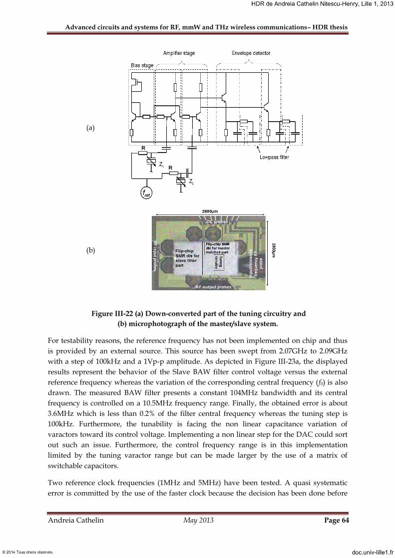
Advanced circuits and systems for RF, mmW and THz wireless communications– HDR thesis
Andreia Cathelin May 2013 Page 64
(a)
(b)
Figure III-22 (a) Down-converted part of the tuning circuitry and
(b) microphotograph of the master/slave system.
For testability reasons, the reference frequency has not been implemented on chip and thus
is provided by an external source. This source has been swept from 2.07GHz to 2.09GHz
with a step of 100kHz and a 1Vp-p amplitude. As depicted in Figure III-23a, the displayed
results represent the behavior of the Slave BAW filter control voltage versus the external
reference frequency whereas the variation of the corresponding central frequency (f0) is also
drawn. The measured BAW filter presents a constant 104MHz bandwidth and its central
frequency is controlled on a 10.5MHz frequency range. Finally, the obtained error is about
3.6MHz which is less than 0.2% of the filter central frequency whereas the tuning step is
100kHz. Furthermore, the tunability is facing the non linear capacitance variation of
varactors toward its control voltage. Implementing a non linear step for the DAC could sort
out such an issue. Furthermore, the control frequency range is in this implementation
limited by the tuning varactor range but can be made larger by the use of a matrix of
switchable capacitors.
Two reference clock frequencies (1MHz and 5MHz) have been tested. A quasi systematic
error is committed by the use of the faster clock because the decision has been done before
R
R

Advanced circuits and systems for RF, mmW and THz wireless communications– HDR thesis
Andreia Cathelin May 2013 Page 65
achieving the steady state. The Figure III-23b capture has been done for a 2.083GHz input
frequency and the measured signal is the BAW filter control voltage.
(a)
(b)
Figure III-23 Measurement results for the tuning circuitry: (a) Behavior of the BAW filter
(control voltage) with respect to the external fref; (b)Vctrl settling
Filte
r re
sp
on
se
Filte
r re
sp
on
se

Advanced circuits and systems for RF, mmW and THz wireless communications– HDR thesis
Andreia Cathelin May 2013 Page 66
Table III-4 is resuming the electrical performances of the presented tuning circuitry.
Parameter Value
Tuning precision 100kHz Error on the BAW filter central frequency < 0.2% Settling time for a 4bits tuning circuit clocked at 1MHz 4µs Power consumption (2.54…4mA) X 2.5V Tuning circuit area 0.15mm²
Table III-4 Tuning circuitry electrical performances
III.6 OTHER CO-INTEGRATED CIRCUITS USING BAW DEVICES:
OSCILLATORS, PHASE NOISE INTEGRATED TEST-BENCH
In order to further demonstrate the system level improvements brought by the co-
integration between BAW devices and regular IC’s, several other circuits have been studied.
A short discussion will be presented about two different designs:
The first one is a basic building block in any communication circuit: an oscillator.
The second one is a newcomer solution among fully integrated IC circuits: an
integrated test-bench for phase noise measurements.
III.6.1 A 2GHZ BICMOS OSCILLATOR WITH FLIP-CHIP MOUNTED BAW RESONATOR
The study of such of a basic building block has been performed in order to check if the
stringent requirements in terms of phase noise coming from the GSM standard can be
attained with a very simple oscillator structure enhanced by a BAW device [VI.10.27].
The oscillator is implemented using the well-known Colpitts technique, as presented in
Figure III-24. A negative resistance is created by a bipolar device in a common collector
configuration. The inductive behavior of the BAW resonator in the fs-fp frequency band is
exploited to generate the oscillations by resonating with the load capacitance CL. The
oscillation frequency is given by:
Lo
msosc
CC
Cff
21
(III-9)
where
21
21
CCC
CCCCL
; C from the bipolar transistor small-signal equivalent structure

Advanced circuits and systems for RF, mmW and THz wireless communications– HDR thesis
Andreia Cathelin May 2013 Page 67
Figure III-24 BAW based BiCMOS oscillator
The design has been carefully optimized in terms of phase noise by maximizing the
oscillation amplitude while not having to deal with the 1/f noise region of the intrinsic BAW
device.
The very tiny chip integrated in the 0.25µm BiCMOS process from STMicroelectronics has
been flip-chipped bump assembled together with a SMR die, as depicted in the next figure.
The co-integration has been performed in this case by taking into account and minimizing
the electromagnetic coupling between the two dies, as it can be observed by the quality of
the measurements as well as the good concordance between measurements and simulations.

Advanced circuits and systems for RF, mmW and THz wireless communications– HDR thesis
Andreia Cathelin May 2013 Page 68
Figure III-25 BAW-IC co-integrated oscillator
Figure III-26 Measured oscillator phase noise compared with simulated data
Finally, this very tiny chip with simplistic schematic is compliant with the most stringent
phase noise specifications (i.e. the GSM ones, both for the Rx band @ 100kHz: -111dBc/Hz
and for the Tx @ 20Mhz offset from the carrier: -158dBc/Hz). It also compared positively
with the oscillator’s state of the art early 2007, when it has been published at ISSCC (see
Table II-1).
mW
P
f
ffLFOM dc
m
om
1log10log20)(
(III-10)

Advanced circuits and systems for RF, mmW and THz wireless communications– HDR thesis
Andreia Cathelin May 2013 Page 69
Table III-5 Comparison with state of the art upon ITRS road-map FoM (as of early 2007)
(for the detailed references index in the table, see [VI.10.27])
III.6.2 AN INTEGRATED PHASE-NOISE MEASUREMENT TEST-BENCH USING BAW DEVICES
The motivation for this research work is multiple.
First of all, from a system level perspective. In integrated wireless transceivers, most
of the times (and at least upon the state of the art of 2006), the system and hence each
building block was specified in such a way that at any moment of its life it can satisfy
all the system specifications. Any moment means in any corner of process, voltage
and temperature (PVT) conditions, and irrespective of the ageing effects. Meaning
that approximately 80% of its life, the full system is over-specified in order to still
comply for the worst case, implying a much larger than needed power consumption.
One of the major metrics in a wireless system (especially very demanding ones, such
as GSM) is the Phase Noise of the Local Oscillator. Its degradation is automatically
seen in macroscopic system level parameters, such as for example the Bit Error Rate
(BER). Hence, the idea here is to be able to have an on-chip measurement circuit for
the instantaneous phase noise and adapt the bias of the Local Oscillator generation
consequently upon the need (see Figure III-27); or for example have on chip several
oscillator cores and choose the one which fits the best at a given moment. A BAW
device co-integrated with classical IC permits to have a very low phase noise

Advanced circuits and systems for RF, mmW and THz wireless communications– HDR thesis
Andreia Cathelin May 2013 Page 70
generated by the measurement system at decent power consumption, hence not
masking the system metric which is under test.
An in-situ integrated test bench can be useful as well for the process features
characterization on the BAW devices itself, such as:
o For Initial Electrical Wafer Sort EWS for trimming batches during the
fabrication (i.e. determine which on wafer sites need extra-loading)
o For Ageing test (BAW phase noise is an indicator for the device ageing)
o For BAW devices characterization, for different input power signals
An on-chip integrated phase noise test bench can also be useful for a high purity
frequency synthesizer design: provide cancellation of the phase noise by a closed
loop from a phase noise measurement to the synthesizer control.
Figure III-27 Example of a wireless transceiver with in-situ BAW integrated phase noise
measurement test bench
A phase noise measurement bench is generally costly laboratory equipment, based on active
references or long delay lines, including low noise amplifiers and phase detectors. The
device under test may either be a frequency source (ex : a VCO) or a two port system, such
as an amplifier, a digital circuit… In the first case, the phase noise measurement bench must
include a frequency reference element, either passive (resonator, delay line) or active
(reference source). In the second case, it is mainly based on a low noise phase detection
process. A special case of two ports devices characterization is the measurement of
piezoelectric resonators noise, which is very difficult to perform using conventional phase
noise measurement techniques on 50 Ω loads. Indeed, these devices need different
impedances conditions to take benefit of their series or parallel resonances. While realized

Advanced circuits and systems for RF, mmW and THz wireless communications– HDR thesis
Andreia Cathelin May 2013 Page 71
on a chip, the input and output impedances can be controlled and the resonator is
characterized in the same conditions it experiences when it is included in a circuit.
Figure III-28 Typical topology of a phase noise measurement bench, in the configuration
for source measurement (frequency discriminator). The residual phase noise
measurement system is the same, with the resonator substituted by the device under test
Figure III-28 represents the typical circuit topology of such a phase noise measurement
bench [VI.10.60]. The main device is a phase detector, generally realized with a mixer with
the two signals (LO and RF) maintained close to the phase quadrature (±90°). The phase
detector is followed by a baseband amplifier, which should feature an equivalent input low
frequency noise lower than the output noise of the phase detector.
If the purpose of the measurement bench is to characterize the frequency source, the
resonator is used as the frequency reference element, and is part of the measurement bench.
It allows, thanks to its large phase to frequency slope (dφ/df), the conversion of the
frequency fluctuations of the source into phase fluctuations, which are then detected by the
phase detector.
If the purpose of the measurement bench is to measure the residual phase noise of two ports
devices, such an amplifier, the device under test (DUT) replaces the resonator, but a
frequency source should be available in the system. This oscillator must be tunable and,
above all, must feature low AM and FM noise. The AM noise is the most critical specification
in this case, because the FM noise is simply removed by equilibrating the delay in the two
arms of the phase detector. In the case of a resonator measurement, the problem of the
parasitic FM noise detection of the source is solved by measuring two identical resonators,
one in each arm of the phase detector, thus canceling the delay caused by one resonator (see
also Figure III-29). The resulting phase noise is the addition of the phase noise of the two
resonators, i.e. a phase noise increased of 3 dB compared to a single resonator, if the
resonators are identical. Finally, in the case of the measurement of frequency conversion
devices (frequency dividers, multipliers…), once again two identical devices must be used,
in order to reach the same frequency on the RF and LO ports of the mixer.

Advanced circuits and systems for RF, mmW and THz wireless communications– HDR thesis
Andreia Cathelin May 2013 Page 72
Figure III-29 Principle schematic of a differential measurement test-bench
To illustrate one of these concepts, we have decided to implement an integrated test-chip
able to measure the phase noise of individual BAW resonators. The circuit presented in
Figure III-29 has been realized using a co-integration between a 0.25µm BiCMOS chip and an
SMR BAW one. All the signals after the frequency generation are differential.
The integrated frequency synthesizer is based on a LC differential VCO, which features a
phase noise of -80 dBc/Hz at 10 kHz offset from a 7.5 GHz carrier, and on a PLL realized
with a digital prescaler. The PLL allows the locking of the VCO on a low frequency reference
source (30 MHz) and the generation of stable signals with a 30 MHz step on the whole VCO
locking range (6.8 GHz to 8 GHz). Only the reference source (quartz oscillator) is maintained
outside the chip.
The output of the frequency synthesizer has to feed a power splitter. As the signal at the
input of the mixer later on the frequency detection chain has to be in quadrature, this can be
solved at this stage by generating signals already in quadrature. In order to implement a
quadrature power splitter, a digital frequency divider has been used [VI.10.44]. This circuit
is based on D flip-flop cells and generates four output signals which are all in phase
quadrature (0°, 90°, 180° and 270°). An important optimization work has been focused on
the D flip-flop topology, and more precisely on the current source of this differential
element, in order to optimize the circuit phase noise (see Figure III-30). The measured noise
floor of this structure is -164dBc/Hz at 100 kHz offset from a frequency of 3.5GHz.
Figure III-30 Optimized frequency divider with simplified D-latch implementation

Advanced circuits and systems for RF, mmW and THz wireless communications– HDR thesis
Andreia Cathelin May 2013 Page 73
The active phase detectors (mixers) are designed using bipolar Gilbert cell mixers with
resistive loads. The circuit presents a phase noise sufficient low for the circuit needs, and
needs to be fed with a relatively low LO input.
The low noise amplifier must feature an equivalent input noise level lower than the output
noise of the phase detector [VI.10.43]. Using the resistive loads mixer, the phase detection
coefficient is (a little higher but) close to the phase detection coefficient of a passive mixer,
and the amplifier performance should be as close as possible as the one of the best
operational amplifiers. Such instrumentation amplifiers feature an equivalent voltage noise
floor in the range of 1 nV/√Hz, and a 1/f noise corner frequency lower than 1 kHz. The goal
has thus been to integrate an amplifier with similar performances (see Figure III-31).
Figure III-31 The integrated instrumentation low noise amplifier
Figure III-32 The integrated instrumentation amplifier measured phase noise
The BiCMOS amplifier fulfills the noise specifications (see Figure III-32), and it compares
positively with the state of the art (see Figure III-33).

Advanced circuits and systems for RF, mmW and THz wireless communications– HDR thesis
Andreia Cathelin May 2013 Page 74
Figure III-33 Comparison with state of the art; instrumentation amplifiers noise and
power consumption features; “this work” means the 0.25µm BiCMOS amplifier
integrated in a stand-alone version
The full BiCMOS chip is depicted in Figure III-34. It has been co-integrated via flip-chip
assembly method with a four identical SMR devices chip. The measured phase noise (see
Figure III-35) is the one of the four devices (incoherent addition of the noise of each device),
which is effectively higher than the noise floor. The phase noise of a single resonator can be
deduced from this plot by subtracting 6 dB to this curve. The reader can mention the
excellent noise floor of the integrated on-chip measurement setup itself, which proves once
more the interest for on-chip integrated phase noise measurement test-benches.
Figure III-34 Microphotograph of the BiCMOS test-chip for integrated phase-noise
measurement test-bench

Advanced circuits and systems for RF, mmW and THz wireless communications– HDR thesis
Andreia Cathelin May 2013 Page 75
Figure III-35 Measured phase noise of the four SMR resonators, and phase noise floor of
the measurement bench
(NOTA: measurements performed at LAAS Toulouse phase noise measurement facilities)

Advanced circuits and systems for RF, mmW and THz wireless communications– HDR thesis
Andreia Cathelin May 2013 Page 76
III.7 CONCLUSIONS AND PERSPECTIVES
BAW resonators may be considered as parented to a kind of mid-Q quartz resonators (their
Q-factor is only around 1000), but they show the very interesting feature that their
processing permits to build on one chip filters or any other structures of designer-defined
ad-hoc schematic and layout. Moreover, their size (and chip height) is compatible with the
ones found usually in regular ICs. Thus, these BAW chips may be co-integrated with regular
Silicon dies by using for example flip-chip bumping assembly technology.
Providing this kind of piezo-electric resonators to the regular Silicon IC world opens new
perspectives on system and circuit level.
From a system perspective, for example, the regular transceiver architectures for wireless
applications can be revisited towards a “Sense and React way of life” [VI.11.5]. The
frequency behavior of BAW resonators in terms of quality factor and phase noise is several
orders of magnitude better than those of the classical Silicon devices. Hence, circuits
“fabricated” with BAW devices can serve as reference measurements on chip for Sensing the
actual behavior of Silicon-based parts of the circuit and through a feed-back loop making
React the system to the instantaneous need with respect to external and internal world. An
example of in-situ integrated test-bench for phase noise measurements for this kind of
Sense&React system architectures has been presented in this chapter.
From a circuit level perspective, these high quality resonators enhanced with active Silicon
“intelligence” open the way to the co-integration of tunable BAW filters. At the time period
when this research had been started (toward 2005), it was considered that they can be a
solution for the on-chip integration of demanding blocker filtering in mobile cellular
applications in the 1 to 5GHz frequency band. Nowadays, other pure IC solutions of high
quality filtering by high speed switched capacitor solutions have been invented, like for
example the work performed in the team of Professor B. Nauta. The on-chip tuning can
serve for process and temperature compensation of the BAW device, but also for the
electrical frequency response variation of the full filter. An example of BAW-based
electrically tunable filter for W-CDMA receiver applications and its tuning integrated
circuitry has been presented at the beginning of this chapter. And finally, novel filter
architectures can be derived by exploiting the extra resonant frequencies of these BAW
devices at lower frequencies.
Other individual blocks can take full benefit of this high quality resonant factor. Namely the
on-chip integrated oscillators, where simple topologies using BAW devices permit to obtain
very performing phase noise behavior, at the extent of low power consumption. A very
simplistic 2GHz oscillator using BAW-IC co-integration has been presented as well in this
chapter, illustrating the opened possibilities.

Advanced circuits and systems for RF, mmW and THz wireless communications– HDR thesis
Andreia Cathelin May 2013 Page 77
IV. MMW AND THZ DESIGN IN DEEP SUBMICRON CMOS
TECHNOLOGIES
IV.1 PREAMBLE
Some 6 to 7 years ago, there has been a big interest showing up in the semiconductor
industry for applications in the millimeter wave frequency band. From a technological point
of view, this became possible thanks to the very high frequency performance of deep
submicron CMOS nodes and BiCMOS dedicated processes. From the application point of
view, this came from the need of more and more bandwidth for wireless communications,
targeting higher and higher data-rates. The traditional 1 to 10GHz band shows up to be
more and more crowded, and when increasing the wireless data rates to around 1Gb/s and
more, the signal theory shows that the most power efficient wireless communications should
have carriers in the millimeter wave bands, where a larger amount of absolute bandwidth
can be allocated much easier. As well, all the safety wireless applications for automotive and
healthcare see also growing interest in the (Bi)CMOS technology.
At STMicroelectronics, a small R&D group has hence been created at that time in order to
investigate integrated (Bi)CMOS design in these frequency bands. At the very beginning of
this adventure, I was in charge of establishing an industrially reliable design methodology
for millimeter wave circuits; the first section of this chapter deals with this presentation. This
work is related also to the PhD studies of Baudouin Martineau and Nicolas Seller, in
collaboration respectively with IEMN Lille (professor François Danneville) and IMS
Bordeaux (professor Jean-Baptiste Begueret).
The next part of this chapter deals with the design of several circuits and systems for
millimeter wave applications in the 60GHz frequency band. First, an RF-band traditional
double heterodyne architecture has been experimented for the design of a CMOS65
transceiver for WirelessHD applications. This work has been carried out in a common
industrial research team between ST and CEA-Leti, and my personal contributions came for
the choice of the analog base-band solutions and the global module antenna and packaging
solution, design and implementation. At the time when this work has been published at
ISSCC (2011), it was the first SiP mmW module compliant with the WirelessHD standard.
Then, two novel alternative architecture studies for the 60GHz band are presented and proof
of concept Silicon implementation has been performed. One, an alternative solution for
beamforming on the LO chain using Coupled Oscillators Array with Injection Locking is
based on the PhD work of Mathieu Egot, co-supervised with professors Andreas Kaiser and
Nathalie Rolland from IEMN. The other one is a new mmW transmitter architecture for high
data rate systems pushing towards the antenna the digital to analog interface, in a Software
Defined Radio approach. This is based on the PhD work of Jonathan Muller, co-supervised
with professors Andreas Kaiser from IEMN and Ali Niknejad from UC Berkeley.
The last part of this chapter treats about an extension of this millimeter vawe studies
towards the TeraHertz frequency band (above 300GHz). This is the fruit of the collaboration

Advanced circuits and systems for RF, mmW and THz wireless communications– HDR thesis
Andreia Cathelin May 2013 Page 78
with professors Ullrich Pfeiffer from the University of Wuppertal and Andreas Kaiser from
IEMN, the PhD student being Hani Sherry. The goal of this extreme advanced R&D work is
to prove CMOS technologies capabilities above the traditional transistor’s fT frequency. It
has been proven that thanks to the self-mixing phenomena in the channel of a MOS
transistor, THz detection can be done with regular CMOS technology. Our research team is a
world pioneer in this field, and we have proven the first Silicon integration ever of a 1K-
pixel THz camera operating from 600 to 1000GHz. A new field of applications can hence be
targeted by miniaturized CMOS circuits: from safety and security harmless imaging
inspection, medical and biology water content detection to dangerous gas detection through
very wide band spectroscopy. This work has been world-wide recognized by the Jan Van
Vessem Award for Best European Paper at ISSCC 2013, and by the Innovation Prize of the
2012 STMicroelectronics Technology Council. Thanks to these outstanding results,
STMicroelectronics has adopted the THz imaging technology on its product road-map, and
became hence the first big semiconductor company to target such products implementation.
IV.2 TARGET APPLICATIONS IN THE MMW BAND
In high frequency electronics books, the millimeter wave band is defined in the frequency
range from 30GHz up to 300GHz, thus for a wave-length of 10mm down to 1 mm [VI.11.1].
When looking from a frequency domain perspective, the immediate advantage foreseen is a
larger bandwidth (5% of 60GHz gives 3GHz, whereas only 300MHz at 6GHz). This feature
enhances communications with a very high speed data rate, hence providing an answer to
the continuous race on increased data rate wireless communications (Figure IV-1).
Figure IV-1 Different wireless communications standards in the race for more data rate
The wave-length domain is also very promising, because it opens interesting perspectives
for reduced area SiP or SoC antenna integration, and also a better resolution for any radar or

Advanced circuits and systems for RF, mmW and THz wireless communications– HDR thesis
Andreia Cathelin May 2013 Page 79
imaging application. The usage of directional antennas permits longer distance
communications. The propagation conditions in the millimeter wave frequency band offer
also some interesting features. The rain attenuation (5dB/km at 60GHz) and the atmospheric
oxygen absorption in the 60GHz band (17dB/km in the 57 to 64GHz band) permit the
development of short-range radio links with excellent immunity to blockers and intrusions
and also enhances the frequency re-use, thus a larger number of users. (see Figure IV-2).
Figure IV-2 Attenuation coefficients for several substances over the frequency band
Having in mind all these considerations, since the last tene years, several applications
promising excellent economical revenues for Silicon technologies are born. Concerning high
data rate communications (0.5 to 5… 10Gb/s), two type of applications are typically
targeted. First of all (see Figure IV-3), the so called Last Inch applications for all kind of
WPAN accesses are oriented for wireless uncompressed HD-video streaming (W-HDMI) or
for ultra fast file transfers. As an example, the HDMI needed raw data rate is 1.5Gb/s for a
1920x1080i resolution, whereas going to 1920x1080p demands a 3Gb/s data rate. All these
applications lay typically in frequency bands going from 57 to 66GHz, depending on
geographical zones. Due to high commercial potential and broad industry support for
communications in this band, groups of people are working towards standardization (IEEE
802.15.3c). In the meanwhile, several consortiums head for specific applications such as
WirelessHD for 10GB/s or plus for in-door consumer applications, and WiGig for multiple
data rate (up to 1…3Gb/s) for handheld wireless devices, including also a merger with the
WiFi application.
Telecom backhauls are usually put into the Last Mile application category, concerning
mostly point-to-point links in licensed E-Band (71-76GHz and 81-86GHz). The propagation
characteristics in these frequency bands give an attenuation value around 2dB/Km, thus
high frequency reuse and huge theoretical connectivity could be envisaged.

Advanced circuits and systems for RF, mmW and THz wireless communications– HDR thesis
Andreia Cathelin May 2013 Page 80
Figure IV-3 Indoor network scenario (HDR last inch) and interfacing to the outdoor
network (HDR last mile)
Low data rate communications, usually demanding ultra low power consumption, target
mostly sensor network applications. These ultra low-power devices may be organized into
intelligent ad-hoc networks providing personal localization and detection inside a room
area. They tend to open also new horizons towards non-intrusive imaging for medical and
security applications, and the targeted frequency bands are at 94GHz and above 100GHz.
The second brand of applications targeting the millimeter-waves band is aimed for
automotive (see Figure IV-4). Adaptive cruise control items for automobiles in the 76-77GHz
band (Long Range Radar) or anti-crash, Stop & Go items in the 77-81GHz band (Short Range
Radar) are starting to get embedded in a major part of new vehicles. For ground to vehicle
and vehicle to vehicle links, the 63-64GHz frequency band is targeted, with high speed data
links as describes in the previous paragraphs.
Figure IV-4 Example of mmW automotive applications contributing to road safety
IDU
+
MODEM

Advanced circuits and systems for RF, mmW and THz wireless communications– HDR thesis
Andreia Cathelin May 2013 Page 81
IV.3 BUILDING A ROBUST DESIGN METHODOLOGY FOR MMW CIRCUITS IN
DEEP SUBMICRON CMOS
The millimeter-waves market segment has been historically held since decades by the III-V
semiconductors, thus pushing these applications to some niche market with respect to the
total market volume in all semiconductors industry, given the high manufacturing cost and
reduced integration scale of the III-V solutions [VI.13.1]. Two phenomena bring since
several years full Silicon technologies as the technology integration platform for millimeter-
waves designs. First of all, the very high frequency performances of the Silicon active
devices (bipolar and CMOS) have dramatically increased over the past years, featuring both
fT and fmax close or higher than 200GHz. And secondly, the market has expressed its need for
low-cost consumer products in the millimeter-waves range, as described in the previous
section.
IV.3.1 SILICON ACTIVE DEVICES ENABLING DESIGN IN THE MMW RANGE
Heterojunction Bipolar transistors offer some advantages compared to CMOS devices such
as their lower 1/f noise, the higher output resistance and the higher voltage capability for a
given speed. The wide technological offer on the market today proposes HBT with fT >
200GHz and even sometimes fmax > 300GHz, as depicted in figures 1 and 2. Different types of
E-B structures are presented, but those permitting to obtain fT > 200GHz and fmax > 300GHz
need to present fully self aligned architectures (FSA) and a high performance collector. And
finally, for an HBT, the fmax parameter has reduced sensitivity to layout parasitics.
Figure IV-5 fT – BVCEO chart built with various Si/SiGeC HBTs available in 130-nm
CMOS node. Different architectures with different maturities are compared.
1 2 3 40
50
100
150
200
250
300
350
fT BV
CEO
(GHz.V)
fT BV
CEO
(GHz.V)
450
300
150
QSA-SP-LC / bulk (Prod)
QSA-DP-HP / bulk
(Prod)
FSA-DP-HP / bulk (Devt) (Proto)
FSA-DP-LC / bulk (Devt)
FSA-DP-LC / SOI (Devt) (Proto)
f T (
GH
z)
BVCEO
(V)

Advanced circuits and systems for RF, mmW and THz wireless communications– HDR thesis
Andreia Cathelin May 2013 Page 82
Figure IV-6 fmax – BVCBO chart built with various Si/SiGeC HBTs available in 130-nm
CMOS node. Different architectures with different maturities are compared.
CMOS transistors follow the well-known Moore’s law of scaling, thus leading to always
increasing functional integration. The 65nm node still uses polysilicon gate, but the carrier
mobility is sometimes increased by using several technological solutions. The hole mobility
in PMOS transistors is increased by using 45° rotated devices and for the electron mobility in
NMOS, tensile liner films are used. In order to limit the gate leakage and to further decrease
the effective electrical gate length, high K dielectrics are used as a part of the gate material.
approximation, is independent of the gate oxide thickness. 150GHz and 200GHz fT are
reached in the 65nm node for Low Power (LP) and General Purpose (GP) devices,
respectively. Data gathered from several major semiconductor foundries show good
conformity with the ITRS road-map, as depicted in Figure IV-7, for both bulk and SOI
technologies.
Figure IV-7 fT ITRS road-map and several foundries’ performances.
fT increases for reduced gate length devices thanks to higher transistor transconductance.
Concerning the capacitive part, fT is degraded by a high gate to drain capacitance (called also
the Miller capacitance). From a theoretical point of view, the transistor’s transconductance is
increasing with the reduction of the effective gate length. Nevertheless, for advanced deep
submicron technologies this trend is not straightforward and the features limiting this
4 5 6 7 8 9 10 11 12 130
50
100
150
200
250
300
350
fmax
BVCBO
(GHz.V)
1800
1400
1000
QSA-SP-LC / bulk (Prod)
QSA-DP-HP / bulk
(Prod)
FSA-DP-HP / bulk (Devt) (Proto)
FSA-DP-LC / bulk (Devt)
FSA-DP-LC / SOI (Devt) (Proto)
f max (
GH
z)
BVCBO
(V)
0
50
100
150
200
250
300
350
400
450
20 30 40 50 60 70 80
Lg (nm)
f T(G
Hz)
ITRS roadmap
IBM, VLSI 01,
SOI 130nm HP
ST, 2006, bulk
& SOI 65nm LP
ST, 2007, bulk
45nm LP
IBM, VLSI 07,
bulk 45nm GP
IBM, VLSI 07,
SOI 65nm HP
Intel, IEDM06,
bulk 65nm HP0
50
100
150
200
250
300
350
400
450
20 30 40 50 60 70 80
Lg (nm)
f T(G
Hz)
ITRS roadmap
IBM, VLSI 01,
SOI 130nm HP
ST, 2006, bulk
& SOI 65nm LP
ST, 2007, bulk
45nm LP
IBM, VLSI 07,
bulk 45nm GP
IBM, VLSI 07,
SOI 65nm HP
Intel, IEDM06,
bulk 65nm HP

Advanced circuits and systems for RF, mmW and THz wireless communications– HDR thesis
Andreia Cathelin May 2013 Page 83
evolutionary trend are the reduced gate oxide thickness, the active zone doping increase and
the low doped drain regions (LDD).
Figure IV-8 fmax ITRS road-map and several foundries’ performances
High fmax values have also been reported for CMOS devices, such as 200GHz on a 65nm LP
node. Fig. 2 presents fmax evolution with respect to the effective gate length, for several deep
submicron technologies coming from different silicon manufacturers (for bulk and SOI). The
fmax of CMOS devices, which should correlate to the performance of large signal operation
blocks such as mixers, oscillators and power amplifiers, is very sensitive to layout parasitics
and also to the choice of the transistor’s finger width. An optimal finger width is chosen for
the majority of millimeter wave circuits, all the solutions seem to converge towards values
lower than 5µm, with two sided gate contacts. A study of this trend is illustrated in Figure
IV-9, where the influence of transistor’s layout on the fT and fmax parameters is evaluated on
several transistors with the same total equivalent size. This technology trial study has been
held on a SOI technology from STMicroelectronics, but it may of course be extrapolated to
any CMOS process. The transistor is divided into several identical cells, and each cell is an
interdigited device with a given unitary finger width.
Figure IV-9 Influence of MOS transistor layout over fT and fmax parameters. The transistor
size is n*(Nf*Wf*Lg) in µm, n = number of transistor cells in parallel, Wf = finger width,
Nf = number of transistor fingers per cell, Lg = gate length (data from
STMicroelectronics)
0
100
200
300
400
500
600
0 20 40 60 80 100
Lg (nm)
f max
(GH
z)
ITRS 2006
Intel, IEDM06,
bulk 65nm HP
IBM, VLSI 01,
SOI 130nm HP
IBM, VLSI 04,
SOI, 90nm HP
IBM, IEDM 05,
SOI 65nm HP
ST, 65nm LP,
SOI & bulk, 07
ST, SOI 130nm,
01
Fujitsu, IEDM
01, SOI
IBM, VLSI 07,
bulk 45nm
0
100
200
300
400
500
600
0 20 40 60 80 100
Lg (nm)
f max
(GH
z)
ITRS 2006
Intel, IEDM06,
bulk 65nm HP
IBM, VLSI 01,
SOI 130nm HP
IBM, VLSI 04,
SOI, 90nm HP
IBM, IEDM 05,
SOI 65nm HP
ST, 65nm LP,
SOI & bulk, 07
ST, SOI 130nm,
01
Fujitsu, IEDM
01, SOI
IBM, VLSI 07,
bulk 45nm
0
40
80
120
160
200
10 100Ids(mA)
f T (GHz)
0
40
80
120
160
200
fmax(GHz)
Ft 8*(2*5*0.12) 2GA
Ft 8*(2*5*0.12)
Ft 2*(2*20*0.12)
Ft 8*(1*10*0.12)
Fmax 8*(2*5*0.12) 2GA
Fmax 8*(2*5*0.12)
Fmax 2*(2*20*0.12)
Fmax 8*(1*10*0.12)
fmax with 2 gate access, Wf = 5µm
fmax with different Wf
NMOS, Lpoly 90nm
130nm SOI process STMicroelectronics
Wf=20µm
Wf=5µm
Wf=10µm

Advanced circuits and systems for RF, mmW and THz wireless communications– HDR thesis
Andreia Cathelin May 2013 Page 84
Several transistor layout topologies are used in order to minimize the extrinsic parasitic
elements added to the intrinsic transistor core. The fmax parameter is extrapolated from very
sensitive high frequency S parameter measurements, and may sometimes suffer from the de-
embedding technique. The transistor layout structure presented in [VI.10.32] is depicted in
Figure IV-10. In this case the transistor is divided into two equal parts with a double
contacted gate. This allows minimizing parasitic capacitances and gate resistance while
using coplanar access. Source contacts are located on the transistor periphery making easier
the contact to the coplanar ground plane. Finally, this structure allows an impedance
matched access towards and from the active device to the rest of the circuit.
Figure IV-10 Layout of n-MOS transistors to maximize mm-wave performances and to
limit discontinuity
Table IV-1 presents a comparison between the presented transistor layout and a classical in-
line transistor structure. Both structures have 2 sided gate contacts. The extrinsic parasitic
elements in this table correspond to an electrical model on the top of a core BSIM4 electrical
model presented here as to be the intrinsic NMOS transistor model (see also Figure IV-11).
The intrinsic electrical core model comprises the front-end device plus the contacts and
Metal 1 layer on the top of it.
CPW
Source
Source
DrainGate
Source
Source
DrainGate
Source
Source
DrainGate
Source
Source
DrainGate

Advanced circuits and systems for RF, mmW and THz wireless communications– HDR thesis
Andreia Cathelin May 2013 Page 85
Extrinsic parasitic elements
In-Line Device
Figure IV-10 Device
Cgs (fF) 6.4 3.7
Cgd (fF) 0.3 3.2
Cds (fF) 5.3 4.4
Rs (Ω) 0.1 0
Rd (Ω) 0.1 0.1
Rg (Ω) 4 0.35
Ls (pH) 4 0
Ld (pH) 4.5 2
Lg (pH) 4 2
Extrinsic fT (GHz) 118 138
Extrinsic fmax (GHz) 125 194
Table IV-1 Comparison of extrinsic small-signal equivalent circuit parameters for an in-
line transistor and the structure presented in Figure IV-10.
LP CMOS 65nm transistor with intrinsic fT ~ 160GHz and fmax ~ 200GHz, Wtotal = 60µm,
Lg = 60nm , Wfinger = 1µm, 6Me BEOL (data from STMicroelectronics)
Figure IV-11 Extrinsic parasitic elements extracted in Table IV-1 for an NMOS transistor
(with respect to a BSIM4 intrinsic model)

Advanced circuits and systems for RF, mmW and THz wireless communications– HDR thesis
Andreia Cathelin May 2013 Page 86
The noise parameter NFmin is also an important marker for the RF and mmW performances
of an active device. The very low noise figure values, presented by deep submicron CMOS
devices nowadays, are very difficult to measure with an excellent accuracy, as the de-
embedding is very complex in the high frequency range. This parameter is strongly
degraded by high gate and source parasitic resistances, thus being layout dependent. Figure
IV-12 presents some NFmin data, gathered from two Silicon foundries and presented with
respect to the ITRS road-map. One may observe that similar RF noise behavior may be
obtained from different technology nodes transistors, depending on the transistor’s
architecture.
Figure IV-12 NFmin ITRS road-map and several foundries’ performances
A very interesting scaling feature has been pointed out by researchers from the University of
Toronto, regarding GP bulk and SOI NMOS transistors from different technology nodes. It
has been shown that, as a result of constant-field scaling, the peak fT (~ 0.3mA/µm), peak fmax
(~0.2 mA/µm) and optimum noise figure NFmin (~ 0.15mA/µm) current densities are
unchanged from one technology node to another (see Figure IV-13 and Figure IV-14). This
has been proven by different foundries Si measurements with technology nodes from
0.25µm down to 90nm. This feature is very convenient when porting CMOS design from one
technology node to another and provides a rule of thumb for early mmW designs.
For HBT devices from different technology nodes, this constant current density for peak fT is
not observed, as depicted in Figure IV-15.
0
0.2
0.4
0.6
0.8
1
1.2
0 10 20 30
Frequency (GHz)
NF
min
(d
B)
ITRS L=45nm @ 5GHz
ITRS L=65nm @ 5GHz
Bulk 45nm, IBM,
VLSI07
SOI PD, 65nm LP, ST

Advanced circuits and systems for RF, mmW and THz wireless communications– HDR thesis
Andreia Cathelin May 2013 Page 87
Figure IV-13 Measured fT and fmax as a function of drain current per micron of gate
width for n-channel MOSFETs fabricated in different bulk and SOI technology nodes
(different founders)
Figure IV-14 Simulated NF at 10 GHz as a function of drain current per micron of gate
width in nMOSFETs fabricated in different technology nodes

Advanced circuits and systems for RF, mmW and THz wireless communications– HDR thesis
Andreia Cathelin May 2013 Page 88
Figure IV-15 Evolution trend of the current gain cut-off frequency fT with the collector
current density JC
Figure IV-16 tempt to realize a comparison between state of the art contemporary 130nm
node SiGe:C HBT and 65nm node NMOS devices, for mmW applications. For this
comparison, the dimensions chosen for the two devices are optimal geometries for mmW
design (mostly for low power linear operation). The first observation is the current
difference for the peak value of fT. At 40GHz, the MOS device performs a better noise figure
than the bipolar, but this trend is reversed for frequencies above 60GHz. For a given fmax, the
higher current densities and voltage swing, lower Ccs, along with a higher transconductance,
permit to the HBT to acquire significant advantage over the MOS transistor for large signal
operation blocs such as power amplifiers. Nevertheless, and also to conclude this sub-
paragraph, both devices exhibit RF features compatible with millimeter wave circuit
integration with industrial margin.
Figure IV-16 fT, fmax and NFmin @ 40 GHz vs. current density for 0.13µm BiCMOS and
65-nm LP NMOS (measurements)
8 12 16 20
160
180
200
220
240
260
280
300
f T (
GH
z)
JC @ peak f
T (mA/µm
2)
0.01 0.1 10
50
100
150
200
250
300
350V
CE = V
DS = 1.2 V
BipX 3x0.130x2.5µm²
fT f
max
C065LP 10x(9x0.062x1.0µm²) fT f
max
f T &
fm
ax (
GH
z)
IC / L
E [HBT] & I
DS / W
G [NMOS] (mA/µm)
0
1
2
3
4
5
6
7
8
NFmin
NFmin
NF
min (
dB
) @
40 G
Hz

Advanced circuits and systems for RF, mmW and THz wireless communications– HDR thesis
Andreia Cathelin May 2013 Page 89
IV.3.2 IMPACT OF THE BACK-END OF LINE ON MMW DESIGN
Contrary to what usually happens in analog (and in a given perimeter in RF) design,
information on the active device is not sufficient for the millimeter wave designer in order to
choose the most appropriate technology. For frequencies above 10GHz, each µm of back-end
strip has a significant influence on the electrical behavior of such a circuit.
The trend when moving from one CMOS node to the next is the vertical shrink of the BEOL
together with the decrease of the metal and dielectric thicknesses and of the metal pitch in
order to increase integration density. Diminishing the lateral dimensions (width) of a
metallic path imposes also a shrink on the vertical dimensions (height). The generally used
rule of thumb in this case gives a shape factor of about three between a metal conductor
height and its minimal width. The Back End of Line (BEOL) evolution through technology
nodes from 0.35µm down to 65nm is depicted in Figure IV-17. One may observe that the
general trend is somehow in antinomy with higher and higher working frequencies. In order
to insure a very (and ultra) large scale of integration for the active devices, the first metal
layers become thinner as do the corresponding Inter Metal Dielectric (IMD) layers. The
increase of the integration scale imposes also the use of a larger number of metal levels and
also implies some changes in the nature of the metallic materials used. The first technology
generations developed for RF design such as 0.35 to 0.18µm had Aluminum layers. Starting
from the 0.13µm generation node, the metallic layers are made of Copper which permits, for
an equivalent metallic strip conductivity, to diminish the height of the deposited layer.
Figure IV-17 BEOL evolution for several technology nodes (CMOS based)
(courtesy to Sébastien Pruvost, PhD thesis manuscript)
The connecting line on Figure IV-17 represents the total dielectric height for a microstrip
transmission line built with the last metal layer (for deep submicron technologies, not all the
metal layers are supposed to be used as for a digital design). One can observe that the total
height of dielectric is diminishing from one technology node to another, thus increasing the
influence of the substrate losses on the propagation constant.
BE
OL
th
ickn
ess
(µm
)
IMD (oxide)
Cu (metal)
Al (metal)
BE
OL
th
ickn
ess
(µm
)
IMD (oxide)
Cu (metal)
Al (metal)

Advanced circuits and systems for RF, mmW and THz wireless communications– HDR thesis
Andreia Cathelin May 2013 Page 90
The dielectric oxide permittivity tends to diminish from one technology node to the next
one, in order to limit the coupling effects between two conducting layers. Nevertheless, the
use of thinner layers imposes an increased contribution of Silicon Nitride (in order to limit
the Copper diffusion into the oxide), which presents a higher permittivity.
Per total and to conclude with these considerations, the total Inter Metal Dielectric height
diminishes with the technology nodes and the equivalent dielectric permittivity remains
mostly constant.
For localized passive elements such as inductors, the small metal line pitch together with the
thin dielectric layers induce larger ohmic and substrate losses. For lumped elements such as
transmission lines, the patterned ground shields are not sufficient to limit the attenuation
constant degradation. In order to cope with these design difficulties for mmW circuits,
different trends came out during the latest years. Two families of back-ends may be
distinguished: while the main stream is held by the (deep) sub-micron digital processes
BEOL, the second trend is presenting millimeter-wave dedicated back-end.
In these millimeter-waves dedicated BEOL, the important number of thick metals (3
typically) and the use of thick Inter Metal Dielectrics are beneficial for low losses in the
transmission lines. In counterpoint, it imposes the development and the use of an
application dedicated process, which sometimes may present higher development costs with
respect to standard back end solutions. For a digital BEOL, a large number of metal levels
lower the losses of last metal level transmission lines, but in counterpoint one may look on
the economic impact of processes with up to 10 metal levels.
The availability of High Resistivity (HR) SOI substrates for CMOS VLSI integration proposes
an alternative to these two solutions, by drastically reducing all parasitic losses towards the
substrate while using standard digital back-end of line.
Figure IV-18 illustrates the impact of the several types of back-end and substrate resistivity
on mmW transmission lines [VI.10.28], [VI.10.29].

Advanced circuits and systems for RF, mmW and THz wireless communications– HDR thesis
Andreia Cathelin May 2013 Page 91
Figure IV-18 Measured and *simulated attenuation constants for 50Ω transmissions lines
in different technologies (all lines are compliant with manufacturing design rules)
(data from STMicroelectronics)
Vertical shrink of the BEOL together with the use of Copper layers impose also very drastic
layout design rules in terms of metal densities per very tiny areas and also electromigration
rules especially for high temperature. The deposition method for Copper layers is
damascene, based on the principle of dielectric trenches which are filled with metal followed
by the CMP step which gives the desired level uniformity. However this uniformity
operation is possible only if the underneath metal layers densities are homogeneous all over
the wafer. This implies that either full metal drawing or the absence of metals on a large
wafer surface is not allowed. Thus, the metallization levels must be perforated if their area is
too large and some small tiles of dummy metal must be placed to preserve the homogeneity
if the initial density is too low. It should be noticed that these rules of densities follow the
projection of the technologies in the future, when these constraints will be more and more
severe (smaller control windows). Figure IV-19 illustrates some of these design rules on one
metal level.
Figure IV-19 Example of metal layer design rules
Among the rules to be respected for each metal level, let us quote inter alia:
0
0,5
1
1,5
2
2,5
3
3,5
4
4,5
5
0 20 40 60 80 100
MS BiCMOS9MW
CPW CMOS130nmHR SOI
CPW CMOS65nmHR SOI
CPW CMOS65nmbulk*
MS CMOS65nmbulk*
Frequency [GHz]
Atten
uation
Consta
nt
[dB
/mm
]
0
0,5
1
1,5
2
2,5
3
3,5
4
4,5
5
0 20 40 60 80 100
MS BiCMOS9MW*
CPW CMOS130nmHR SOI
CPW CMOS65nmHR SOI
CPW CMOS65nmbulk*
MS CMOS65nmbulk*
Frequency [GHz]
Atten
uation
Consta
nt
[dB
/mm
]
0
0,5
1
1,5
2
2,5
3
3,5
4
4,5
5
0 20 40 60 80 100
MS BiCMOS9MW
CPW CMOS130nmHR SOI
CPW CMOS65nmHR SOI
CPW CMOS65nmbulk*
MS CMOS65nmbulk*
0
0,5
1
1,5
2
2,5
3
3,5
4
4,5
5
0 20 40 60 80 100
MS BiCMOS9MW
CPW CMOS130nmHR SOI
CPW CMOS65nmHR SOI
CPW CMOS65nmbulk*
MS CMOS65nmbulk*
Frequency [GHz]
Atten
uation
Consta
nt
[dB
/mm
]
0
0,5
1
1,5
2
2,5
3
3,5
4
4,5
5
0 20 40 60 80 100
MS BiCMOS9MW*
CPW CMOS130nmHR SOI
CPW CMOS65nmHR SOI
CPW CMOS65nmbulk*
MS CMOS65nmbulk*
0
0,5
1
1,5
2
2,5
3
3,5
4
4,5
5
0 20 40 60 80 100
MS BiCMOS9MW*
CPW CMOS130nmHR SOI
CPW CMOS65nmHR SOI
CPW CMOS65nmbulk*
MS CMOS65nmbulk*
Frequency [GHz]
Atten
uation
Consta
nt
[dB
/mm
]
wcwt
Total Density
wcwt
Total Density

Advanced circuits and systems for RF, mmW and THz wireless communications– HDR thesis
Andreia Cathelin May 2013 Page 92
- The minimum and maximum density per a given control window (in general
between 20 and 80%)
- The minimum size of an enclosed area in a metallic layer (Wt)
- The minimum and maximum width of a metal stripe (Wc)
All these constraints have to be taken into account at the very beginning of every millimeter
waves design. The ground planes contribute a lot to the metal density filling of the total
area, but also the gap between the transmission line and these ground planes must respect
the metal density rules. The maximum line width is also controlled by DRC rules, thus
limiting the theoretical choices for the transmission lines design. On the other hand, the
central signal stripe width is determined also by electromigration rules depending on the
maximum current density to flow with no damage.
An example of such transmission line on a digital BEOL in the 65nm node is presented in
Figure IV-20 and Figure IV-21. Classical transmission line theory would have imposed that
the ground planes should be built at the same level as the central conducting path, but in the
presented case, in order to respect the metal density rules, the ground planes have also a
vertical dimension in order to fill the space also for the lower level metals. These extra levels
in the ground plane impose extra losses by fringing coupling. 3D electromagnetic field
solvers offer good help for these studies.
Figure IV-20 Coplanar transmission line in a 65nm CMOS digital BEOL (6 Metal layers)
APM6M5M4
M2M3
M1
Gnd GndRF

Advanced circuits and systems for RF, mmW and THz wireless communications– HDR thesis
Andreia Cathelin May 2013 Page 93
Figure IV-21 Top view for the transmission line in Figure IV-20
In order to conclude, the Back-End of Line of the recent technology nodes permits the
integration of passive devices compliant with the design of mmW integrated products. A
digital back-end on standard VLSI CMOS technologies implies rather lossy solutions for the
passives, which have to be overcome by a higher overall current consumption and
sometimes figures of merit (such as Noise Figure). In counterpoint, the use of a standard
VLSI technology permits a good manufacturing flexibility. On the other hand, mmW
dedicated back-end permits passive integration with very low losses, thus lower power
consumption, but the overall production cost is raised by the use of an application dedicated
process.

Advanced circuits and systems for RF, mmW and THz wireless communications– HDR thesis
Andreia Cathelin May 2013 Page 94
IV.4 TOWARDS COMPLEX CIRCUITS AND SYSTEMS FOR MMW
APPLICATIONS
IV.4.1 CLASSICAL ARCHITECTURE: 60GHZ HDR TRANSCEIVER
A fully integrated WirelessHD compatible 60GHz transceiver has been implemented by a
joint ST –Leti design team in which I worked. This design is presented here as an example of
what can be done using traditional RF architectures and today state of the art CMOS
technology in order to address a 60GHz standard [VI.10.56].
Figure IV-22 Frequency plan for the 4 channels allocated in the 802.15.3c standard
The CMOS 65nm circuit is covering the four channels of the WirelessHD standard. The
Silicon die is flip-chipped on top of a low-cost HTCC module which also includes an
external 65-nm CMOS PA and large beamwidth antennas targeting industrial
manufacturability. The module achieves a 16QAM OFDM modulation wireless link with 3.8
Gbps over 1 meter. The transceiver consumption is 454 mW in RX mode (including PLL) and
1090mW in TX mode (including PLL and external PA). This full module implementation
was among state of the art mid 2011 for the given application.
For a single-path transceiver, the link budget gives around a 1-m range for 10-dBm emitted
power and 6-dBi antenna gain. Regarding the frequency channels, the WirelessHD standard
has adopted those defined by the 802.15.3c group (see Figure IV-22). Hence, the required
frequency coverage by the frequency synthesizer (58.32 to 64.8 GHz) is large (frequency
tuning range FTR >10%) , while the required phase noise has to be low. Indeed, system-level
simulations using phase tracking correction show that the phase noise must be lower than
92 dBc/Hz at 1-MHz offset of the carrier.
A sliding-IF architecture is hence proposed for the 60GHz transceiver, as depicted in Figure
IV-23. The frequency plan of the transceiver is hence given by:
32
21
RFLOLO
FFF
(IV-1)
-20dBc
-30dBc
-10dBc
0dBc58.32GHz 60.64GHz 62.64GHz 64.80GHz
2.16GHz
1.76GHz

Advanced circuits and systems for RF, mmW and THz wireless communications– HDR thesis
Andreia Cathelin May 2013 Page 95
Figure IV-23 60GHz transceiver using sliding-IF architecture
Thus, the LO1 and LO2 are in the 20- and 40-GHz bands, respectively. This double-
conversion architecture relaxes the phase-noise constraints with respect to an equivalent
direct conversion scheme, since the phase-noise sources, all coming from the 20-GHz LO1,
are added. Moreover, this double-frequency conversion architecture helps distributing gain,
noise figure and linearity constraints in a balanced way between the active blocks.
The different constitutive elements of the transceiver are designed using classical mmW and
RF design techniques (see for more details paper [VI.9.9]). The final transceiver chip
photomicrograph is given in Figure IV-24.
5 th order
20 GHz 0 ° /90 ° and 40 GHz
PLL
3 th order
90 °
0 °
I2C, Registers, Channel selection, Power
management
PPA
LNA
Mixer
Mixer
40 GHz LO2 Buf
40 GHz LO2 Buf
BB Amps.
IQ Mixers
20 GHz LO1
20 GHz LO1
20 GHz IF Amp.
IQ Mixers BB I - input (50 )
BB Q - input (50 )
BB Q - output (50 )
BB I - output (50 )
60GHz RF out (50 )
60 GHz RF in (50 )
36 MHz Ext. Ref.
Gm - C
Gm - C
20GHz IF Amp.
Gm - C
Gm - C

Advanced circuits and systems for RF, mmW and THz wireless communications– HDR thesis
Andreia Cathelin May 2013 Page 96
Figure IV-24 The 60GHz CMOS 65nm transceiver
A ceramic module has been chosen as a SiP solution holding the CMOS 65-nm transceiver,
external CMOS 65-nm power amplifier, transmit and receive antennas, as well as a few
surface-mounted devices (SMDs) for power supply filtering [VI.10.53]. The module is
implemented in an industrial process five-layer high-temperature cofired ceramic (HTCC)
technology from Kyocera (Figure IV-25). Each ceramic layer is 100 m thick, the internal
metal layers are made of a 10- m-thick tungsten alloy, while top and bottom layers are made
of tungsten with Ni/Au plating (1.27/1.5 µm). The bottom of the module is designed upon a
land grid array (LGA) strategy for standard surface-mount attachment onto a PCB. Two
cavities (2x1.95x0.3 mm3 ) are managed in the module as part of the antennas . The total
module size is 8.5x13.5x0.95 mm3 including ceramic, antennas, chips, and bumps.
The strategy adopted for this implementation is the use of two identical hemispherical
omnidirectional antennas for the RX and TX sides, respectively. They are folded dipoles
placed on top of a metallic ground plane acting as reflector. They present a gain of ~6dBi
over the full 60GHz band.
Transmitter
Receiver
PLL
2.8 mm
3.3 mm

Advanced circuits and systems for RF, mmW and THz wireless communications– HDR thesis
Andreia Cathelin May 2013 Page 97
Figure IV-25 Photograph of the HTCC module with CMOS transceiver, PA and antenna
chips. Cross-section along AA
The full application experiments with this module demonstrated a wireless transmission
range above 1 m in an office-like space for the 16QAM—OFDM HRP2 (3.8 Gbps).
Figure IV-26 Emitted spectrum of the WirelessHD 1080p OFDM - 16QAM HRP2, data
rate: 3.8Gbps (TX, channel 4). Received analog base-band signal in the I (or Q) channel
after 1-meter wireless transmission.
CMOS
transceiver
PA
Rx antenna
Tx antenna
AA
CMOS transceiver Tx antenna
60 GHz feed line
cavity
Rx antenna
-80
-70
-60
-50
-40
Center 1GHz Span 2GHz200MHz/
Ref Lvl -31dBm
5dB/
20dB required for
demodulation
1760MHz OFDM band
Emitted signal Received signal

Advanced circuits and systems for RF, mmW and THz wireless communications– HDR thesis
Andreia Cathelin May 2013 Page 98
This work described the design and fabrication of a complete 60-GHz transceiver SiP for
WirelessHD applications, as of early 2011. The SiP is industrially assembled on an HTCC
substrate that holds the CMOS 65-nm transceiver, the PA, and the RX and TX antennas. It
consumes 454 mW in RX mode and 1090 mW in TX mode, including the frequency
synthesizer which covers the four bands specified by the standard. The module has
demonstrated an OFDM-16QAM modulation wireless link at the four WirelessHD standard
channels over 1-m distance. Table II-1 summarizes the progress on 60-GHz transceivers in
silicon technologies.
This work paved the way for low-cost, mass production of WirelessHD chip-sets. The power
consumption of this solution is for sure over dimensioned, nevertheless at the day of
publication (ISSCC 2011) it was the first full module solution for WirelessHD applications.
Ref. Tech. PDC (mW)
Emitted
Power Channels Integration
Modulation
scheme Package
M.Tabesh
ISSCC 2011
65nm
CMOS
RX/TX/PLL
108/112/29
Psat
(dBm)
4.5
(array)
N/A
Phased array
x4, TX, RX,
PLL
N/A N/A
S. Emami
ISSCC 2011
65nm
CMOS
RX/TX
1250/1820
EIRP
(dBm)
28
2
x32 array
TX/PLL
x32 array
RX/PLL
(separate
chips)
OFDM
16QAM Ceramic
K. Okada
ISSCC 2011
65nm
CMOS 106/186/66
Psat
(dBm)
11
2 Full TRX,
External PLL
BPSK,
QPSK,
8PSK,
16QAM
(SC)
Organic BGA
S.Pinel, ISSCC
2008
90nm
CMOS 129/113/80
Psat
(dBm)
8.4
4 Full TRX, PLL
and ABB
QPSK
16QAM FR4
C.Marcu, ISSCC
2009
90nm
CMOS 138/170/76
Psat
(dBm)
11
1 Full TRX, PLL
and ABB QPSK N/A
S.K.Reynolds,
RFIC 2010
0.12µm
SiGe
BiCMOS
(RX& PLL)
1800 - 4
Phased array
x16, RX, PLL
OFDM
16QAM
Organic
BGA
E. Cohen,
RFIC 2010
90nm
CMOS
RX/TX
500/500
Psat
(dBm)
8
(array)
N/A
Phased array
x32, TX, RX,
No PLL
N/A Alumina
A. Tomkins,
JSSC 2009
65nm
CMOS
RX/TX
151/223
Psat
(dBm)
7.5
N/A TX, RX
No PLL BPSK N/A
This work 65nm
CMOS 374/1010/80
Psat
(dBm)
>16 4
Full TRX,
PLL and ABB
& filters
OFDM
16QAM
HTCC+glass
antennas
Table IV-2 State of the art fully integrated 60GHz transceivers, as of mid 2011

Advanced circuits and systems for RF, mmW and THz wireless communications– HDR thesis
Andreia Cathelin May 2013 Page 99
IV.4.2 NOVEL SYSTEM ARCHITECTURES FOR MMW TRANSCEIVERS
IV.4.2.1 LOCAL OSCILLATOR BEAM-FORMING TECHNIQUES
In this section, we will discuss an alternative solution for beam-forming transceivers to be
used in the 60GHz frequency band. The work has been developed for a transmit path,
nevertheless it can easily be transposed for a receive path as well [VI.10.62].
In order to reach the very high data rate of the WirelessHDTM or WiGig standards especially
for distances larger than 1 meter, transmit/receive arrays with 2D or 3D beamforming are
investigated, particularly in CMOS technology. Beamforming technique requires
controllable identical phase shifts between adjacent RF paths in the array. However, the
realization of phase-shifters at 60GHz on the signal path and achieving good performance
(frequency range, losses, linearity) remains a bottleneck. To overcome these issues, other
beamforming architectures exist. The phase-shifter can be alternatively placed either in
baseband or LO paths providing benefits from lower working frequency. This study
presents the proof of concept for a low power accurately-controlled LO beamforming
solution requiring only a single phase-shifter.
Figure IV-27 Proposed architecture for a 4-path 60GHz LO beam-formed transmitter
The proposed architecture of a 4 path beamforming 60GHz transmitter is shown in Figure
IV-27. The LO beamformed signals generation is similar to the approach described in the
work of K.D. Stephan et al. in 1987 with GaAs MESFET, and is to the authors’ best
knowledge the first attempt of a silicon integration. Four differential phase-shifted LO
signals are generated by a Coupled Oscillators Array (COA). The oscillators at both ends of
the array are injection locked to respectively the primary LO signal and its phase-shifted Φ
copy. The resulting phase-shift between adjacent oscillator outputs of an N oscillators array
is given by:
1
N
(IV-2)
x2 x2
Baseband4
Baseband1
PLLΦ
[20-23GHz] [40-46GHz]
[60-69GHz]
[20-23GHz]
[6.7-7.7GHz]
[4-4.6GHz]
Implemented Circuit

Advanced circuits and systems for RF, mmW and THz wireless communications– HDR thesis
Andreia Cathelin May 2013 Page 100
The maximum available phase-shift between adjacent oscillators is hence given by:
1
2max
N
(IV-3)
An array of 4 coupled-oscillators is implemented here resulting in a theoretical 120°
maximum phase-shift between two adjacent oscillators.
This solution requires only one phase shifter in a low frequency band. Compared to
baseband or other LO solutions, oscillators can be placed near mixers without LO
distribution saving hence power and chip area. And finally, the proposed solution provides
a continuous phase shift generation thus offering increased system flexibility. The solutions
proposed so far provide only discrete phase shift values.
The WiGig standard requires frequency generation at 2.5, 5 and 60GHz with low power
consumption, as the device has to support the 802.11a and d as well as the 802.15.3c
standards. The first attempt of wide range multi-standard frequency generation following
these requests exhibits high complexity and consumes several dozens of mW. The proposed
COA can be injection locked either on a fundamental or on a harmonic signal, while the
resulting phase noise is a copy of the source injecting signal’s noise. Hence, the solution
proposed here becomes very attractive for a full WiGig device. Starting from a <10GHz
frequency synthesis, the 2.5 and 5GHz and also the beam-formed mmW frequencies can be
provided at reduced power consumption and low phase noise.
As a proof of concept, a 4-element coupled oscillators array operating around 20GHz has
been implemented in CMOS65nm.
The key building-block is the differential VCO (see Figure IV-28). The proposed VCO is
based on a classical LC topology. The oscillating core has been optimized for low power
consumption, the low layout area imposing the choice of the on-chip inductor and a wide
tuning range to reach the WiGig specifications. An on-chip transformer is inserted on the
source nodes of the NMOS cross-coupled pair to provide an entry point for the injection
locking signal. The bias current is fed through the center tap on the primary winding. The
transformer’s primary is part of the resonator tank while the secondary makes the
impedance matching between the single-ended injection port and the source of the NMOS
cross-coupled pair. The transformer also acts as a band-pass filter for unwanted harmonics
in injection-locking mode.

Advanced circuits and systems for RF, mmW and THz wireless communications– HDR thesis
Andreia Cathelin May 2013 Page 101
Figure IV-28 Schematic of the proposed VCO with injection locking capability
The coupling network between the 4 oscillation cores should not introduce any additional
phase shift over the complete locking-range of the array (20-23GHz), i.e. requiring a
wideband 0° phase coupling network. λ transmission lines are impractical because of
excessive line length at the given frequency (≈7mm). Hence resistive coupling has been
chosen (see Figure IV-29). A 200Ω resistor is found to be the optimum value. Oscillators are
placed side-by-side. To connect the resistor to the two adjacent oscillators, short
transmission lines (50µm) have been inserted on each side. Due to loading effects, the
maximum phase shift between adjacent oscillators is reduced to around 100°.
Figure IV-29 Anti-symmetrical layout of the coupled oscillators array
The single-ended injection is performed through the transformer’s secondary of the two
peripheral oscillators. The inner oscillators of the array have their injection port shorted to
ground. Coarse and fine tuning signals are common to all oscillators.
Special care must be taken to the oscillator array layout. Indeed all VCO cores are
identical and should be matched. The layout of the VCO was optimized to reduce parasitic
capacitances and the array layout was made completely symmetric to avoid internal phase
errors. Differential coupling layout is not trivial too. Hence each VCO core has an anti-
symmetrical layout in order to avoid signal path crossings. Differential active signals are
only crossing inside each VCO core.
VinjVbias
MN1
Lres
MN2
MP1 MP2
VDD
Vop Von
Vtune
Cfix
VVaractor Bank
B2
B1B1
B0
+ -
- +
- +
+ -
+ -
- +
VCO CORE1 VCO CORE2 VCO CORE3 VCO CORE4
- +
+ -

Advanced circuits and systems for RF, mmW and THz wireless communications– HDR thesis
Andreia Cathelin May 2013 Page 102
For measurement purposes, 0 dB gain single-ended cascode buffers with 50Ω LC output
matching and isolation better than 40dB are also integrated on chip. Thanks to the high
isolation it is possible to measure one output while the three others are not 50Ω -loaded.
Buffers are directly biased by the output DC voltage of the VCOs. For each VCO, only one
buffer is connected to an output pad due to pad limited layout. The other buffer is
terminated with an on-chip 50Ω resistance to preserve signal symmetry.
Different types of measurements confirm good agreement with simulated performance. The
combination of the varactors control and injection locking allows a VCO array locking range
from 20.3 to 23.4 GHz as shown in Figure IV-30. Even in the high temperature case, the
2.5GHz locking-range remains large enough to meet the standard requirements.
Figure IV-31 presents the phase noise performance, for the free-running 20GHz VCO’s and
for the injection-locking conditions; several experiments have been carried out with
fundamental and sub-harmonic injection signals. When locked, the array reproduces the
primary LO phase-noise performance as expected. The spurious rays on the figure
correspond to the RF lab noise signature (between 1 and 8MHz offset). However, the phase
noise slightly increases with the number of the harmonic locking.
Figure IV-30 Measured locking range (LR) vs. temperature (up) and output power
variations vs. input phase-shift (down) for a 22GHz 0dBm input injection signal
-8
-6
-4
-2
0
2
4
6
8
19 20 21 22 23 24
INP
UT
PO
WER
(d
Bm
)
INPUT FREQUENCY (GHz)
LR @ 0°C LR @ 27°C
LR @ 80°C
-10
-9,5
-9
-8,5
-8
-7,5
-7
-6,5
-6
-5,5
-5
-300 -240 -180 -120 -60
Ou
tpu
ts P
ow
er
(dB
m)
22GHz Input Phase-Shift (Deg)
Out4
Out1Out2
Out3

Advanced circuits and systems for RF, mmW and THz wireless communications– HDR thesis
Andreia Cathelin May 2013 Page 103
Figure IV-31 Measured Free-Running and Injection-Locked Phase Noise
Figure IV-33a shows the measured phase shift between adjacent channels for a 22 GHz input
signal. A 60° increase of the input phase-shift produces a 12° output phase shift, which is
close to the expected 10° phase shift at the frequency divider output. The maximum phase
error is less than 5° at 11GHz. The measured phase-shift range obtained is about 100° with a
300° maximum input phase-shift range. Figure IV-32b shows the time domain output
waveforms for a 180° input phase difference at 22 GHz i.e. 30° phase-shift at 11GHz.
Figure IV-32 Chip Micrograph. The active area is 0.23mm²
-150
-140
-130
-120
-110
-100
-90
-80
-70
-60
-50
-40
-30
-20
1,0K 10,0K 100,0K 1,000M 10,000M
PH
ASE
NO
ISE
(dB
c/H
z)
FREQUENCY OFFSET (Hz)
Free-running VCO
External Reference& Locked VCOs
-140
-130
-120
-110
300,0K 3,000M
PH
ASE
NO
ISE
(dB
c/H
z)
FREQUENCY OFFSET (Hz)
EXTERNAL REF @ 22GHz
VCO LOCKED ON 22GHz FUND
VCO LOCKED ON 7.5GHz FUND
VCO LOCKED ON 4.5GHz FUND
VCO Locked on3rd Harmonic
External Reference
VCO Locked On Fundamental
VCO Locked
On 5th Harmonic
Advanced circuits and systems for RF, mmW and THz wireless communications– HDR thesis
Andreia Cathelin May 2013 Page 104
Figure IV-33 Measured output phase-shifts (a) and time domain waveforms at the divide-
by-two output for a 180° input phase shift (b) with 22GHz 0dBm input injection signal.
10
15
20
25
30
35
40
45
50
55
60
-300 -240 -180 -120 -60
11
GH
z O
utp
ut
Ph
ase
-Sh
ifts
(D
eg
ree
)
22GHz Injected Phase-Shift (Degree)
ΔΦ1
ΔΦ2
ΔΦ3
ΔΦtheoretical
-150
-100
-50
0
50
100
150
-100 -50 0 50 100
Am
plitu
de
(m
V)
Time (ps)
Output1
Output2
Output3
Output4
(a)
(b)

Advanced circuits and systems for RF, mmW and THz wireless communications– HDR thesis
Andreia Cathelin May 2013 Page 105
Table IV-3 permits to conclude on this work. As of October 2011, this was the first such
architecture implemented on silicon. The system presents 3GHz locking range around
21.5GHz and can achieve a maximum phase-shift of 100°. The injection locking system
permits to copy the injection source phase noise to the outputs of the locked oscillators
hence the phase noise performance is compatible with the WirelessHDTM and WiGig
requirements. Furthermore, the presented solution permits important power reduction in a
generally power hungry beamforming solution for HDR 60GHz transmitters. The COA
provides a continuous 300° phase-shift when translated at 60GHz whereas the existing
solutions are performing only discrete values. The COA exhibits also low output power
variation vs. phase shift. The proposed coupled oscillators array (COA) architecture can
provide a significant advantage in a system using a low frequency main PLL from which
phase shifted signals at higher mmW range frequency are fabricated.
Stephan et al,
1987
Tabesh et al,
ISSCC 2011
Cohen et al,
RFIC 2010
Valdes-Garcia
et al, ISSCC 2010 This Work
Technology GaAs MESFET 65nm CMOS 90nm CMOS 0.12µm SiGe 65nm CMOS
One Phase
Delay Pdc N/A
(on Baseband
path)
~3mW@1,3V *
(on RF path)
(1 path)*
(on RF path)
(on LO path)
Frequency
Range VHF Band 57-66GHz (15%) 57-66GHz (15%) 57-66GHz (15%) 20-23GHz (15%)
Phase-shift
range /
resolution **
90°
/continuous 45°/5° 360° /90° 360° /11°
300°
/continuous
Phase-
shifter
architecture
COA
(3 VCOs)
(continuous)
Phase rotator
(discrete)
Switched Delay
Passive LC
(discrete 2bit)
RTPS+VGA
(discrete 5bit +
1bit)
COA (4 VCOs)
(continuous)
*Estimated power consumption including power splitters & combiners and excluding buffers &
amplifiers
** Data translated around 60GHz for comparison between different solutions
*** RTPS = Reflective type phase-shifter
Table IV-3 Phase Delay generation inside 60GHz beam-forming solutions;
State of the art performance comparison

Advanced circuits and systems for RF, mmW and THz wireless communications– HDR thesis
Andreia Cathelin May 2013 Page 106
IV.4.2.2 MMW SDR TRANSMITTER FOR HIGH DATA-RATE COMMUNICATIONS
In this section, we address the same kind of high data rate 60GHz applications, while getting
inspired by the Software Defined Radio system knowledge coming from the cellular
communications [VI.9.10].
The concept and upcoming circuit described in this section is one of the first attempts to
introduce digital processing beyond the baseband in wide-band 60GHz transmitters. The
target is to propose an alternative to analog reconstruction filters by introducing digital
oversampling filters combined with high speed DA converters. In a classical transmitter, the
digital baseband signal is converted to the analog domain by a Nyquist rate DA converter
followed by an analog filter to suppress spectral images. Such analog filters need to have a
cut-off frequency of around 880MHz (1.7GHz useful channel bandwidth) and should be of
order 4 or 5 to meet the spectrum mask requirements. Analog passive implementations with
inductors and capacitors require very large silicon area and provide low quality factors.
Appropriate active analog filters have also been shown recently in the context of a receiver.
Oversampling and filtering in the digital domain in combination with direct digital-to-RF
conversion can push the analog filtering to higher frequencies and relax at the same time
filtering requirements. Passive band-pass filters with smaller area can then achieve the
required specifications. Furthermore, digital circuits can be made programmable offering
increased flexibility.
The standard proposes to use either single carrier modulation or OFDM modulation. We
focus our study on OFDM modulation. 4 channels of 1728 MHz bandwidth spaced by 2.16
GHz are available in the 57-65 GHz band. The OFDM signal contains 336 subcarriers of 5
MHz each and is sampled at the I and Q outputs of the digital signal processor at 2.5 GS/s.
Figure IV-34 Proposed digital Transmitter architecture for 60GHz applications
Figure IV-34 shows the proposed 60GHz transmitter architecture. The D-to-A conversion is
merged with the mixer into a so-called DRFC (digital-to-RF converter). To avoid analog
base-band filters, the digital data stream is oversampled prior to D-to-A conversion. In the
oversampling process, images of the baseband spectrum appear at multiples of the initial
sampling frequency and have to be filtered. To meet the spectrum mask requirements, a

Advanced circuits and systems for RF, mmW and THz wireless communications– HDR thesis
Andreia Cathelin May 2013 Page 107
digital interpolation filter is needed. The design and implementation of this filter is reported
in this paper. For the standard targeted here, signal-to-noise ratio and spectrum-mask
specifications require 7 bit resolution.
After filtering and conversion to the analog domain, the first residual image appears at an
offset equal to the sampling frequency. The worst case situation is when channels A1 (or A4)
are used (the two extremity ones, see also Figure IV-22). To avoid that images appear in the
channel on the other end of the RF band, the oversampling frequency must be greater than
the standard’s bandwidth, i.e. 8.64GHz. At the same time, the oversampling frequency
should be an integer multiple of the baseband sampling frequency. The closest frequency
satisfying both criteria is 10GHz, corresponding to a 4x oversampling of the base-band data.
Thanks to the sample-and-hold function inherent to the D-to-A conversion, the first residual
image is attenuated by 20dB. Therefore it can be eliminated by the RF band filters present in
the systems. Pushing the oversampling frequency to higher frequencies would relax the RF
filtering requirements, but is not feasible with current CMOS technologies.
Figure IV-35 OFDM signal up-sampled to 10 GS/s, attenuation of the images with the sinc
function, and spectral mask
The spectrum of the QPSK-OFDM modulated digital signal after up-sampling to 10 GS/s is
depicted in Figure IV-35. Each sample is repeated 4 times. This introduces a sinc function
that provides some attenuation of the images. Further attenuation by about 30dB is
necessary in order to respect the spectrum mask.
As a proof of concept of the full system validity, the designed chip contains the interpolator
section (see Figure IV-34), in a 65nm GPLP CMOS process.
Basically an interpolator is the combination of an up-sampler and a digital filter to remove
the images created by the up-sampling process. Due to the very high frequency operation,
digital IIR filters containing feedback loops are not practical. A FIR filter is therefore used.

Advanced circuits and systems for RF, mmW and THz wireless communications– HDR thesis
Andreia Cathelin May 2013 Page 108
Based on the filter specifications, it has been determined that a 22 coefficient filter is able to
fulfill the requirements with acceptable attenuation at pass-band edges. However, even with
a state of the art technology, the implementation of multipliers at 10 GS/s is not practical.
Therefore, a modified filter architecture using only power-of-two coefficients has been
implemented. Indeed, power-of-two coefficients are realized by wired bit-shifts and don’t
require additional hardware.
Furthermore, it is not necessary to run the complete filter at 10 GS/s. To relax speed
requirements, one could use parallel (poly-phase) architectures at a lower sample rate that
are recombined into a high sample rate output data stream. However, the poly-phase
structure introduces more complex routing and recombination of the output signals is also
critical and involves several adder stages. Alternatively, it is possible to do the up-sampling
in several steps, i.e. two steps in this case. In this way, only a small part of the filter actually
works at the maximum sampling rate. This is the option taken here and is depicted in Figure
IV-36.
Figure IV-36 Partitioned interpolator structure
The next step is to determine a set of coefficients for the first and second interpolator, while
trying to reduce complexity. In order to keep linear phase characteristics, the coefficient sets
are supposed to be symmetric. At this point, filter synthesis tools have been used to find the
required filter order. Finally, we explored a further simplification of the structure by
dividing each of the FIR filters into a cascade of two identical filters.
As a final choice, each of the FIR filters at 5GS/s has 6 coefficients, while each of the FIR
filters at 10GS/s has 3 coefficients. This minimizes the complexity of the filters at 10GS/s
while still meeting the specifications.
At this point coefficients are still floating point coefficients. Simple quantification of the
coefficients does not produce satisfactory results; some optimization has to be produced.
The two criteria used for optimization are in-band ripple and out-of-band rejection. A
genetic algorithm has been programmed to find an optimal set of powers of two coefficients.
The set of optimal coefficients is on a so-called Pareto front showing the optimal stop-band
attenuation for a given pass-band ripple. The designer then chooses the most suitable
compromise between the two criteria. Coefficients could be in the range from 20 to 2-6 given

Advanced circuits and systems for RF, mmW and THz wireless communications– HDR thesis
Andreia Cathelin May 2013 Page 109
the 7 bit dynamic range. However, in practice the range used is from 2-1 to 2-4. The coefficient
sets selected are given in Table IV-4.
Table IV-4 Quantized interpolator coefficients
The final architecture, chosen for this work, is presented in Figure IV-37. The filter output
needs only 7 bit precision. To reduce the computational effort, each FIR output could have
been truncated to 7 bits. However, the attenuation close to the band edge deteriorates
significantly. The internal word length is therefore progressively extended up to 11 bits in
order to avoid saturation and keep the maximum computational precision. Only the filter
output is then truncated to 7 bits.
Figure IV-37 Final internal architecture of the interpolator
A global simulation of an OFDM symbol filtered with the chosen coefficients is shown in
Figure IV-38. Attenuation of signals in the pass band causes phase and amplitude errors in
the constellation responsible for an increase of the error vector magnitude (EVM). The
constellation of a random-data QPSK-modulated OFDM symbol at the interpolator output is
represented on the I/Q chart in Figure IV-39. Sub-carriers close to the band edge are
attenuated with respect to the ones in the center of the band, which leads to this flower petal
representation. The raw EVM before any equalization is 17.83 % which is still compliant
with the standard that requires an EVM < 19% for class 2 devices.

Advanced circuits and systems for RF, mmW and THz wireless communications– HDR thesis
Andreia Cathelin May 2013 Page 110
Figure IV-38 Simulated OFDM signal filtered with final filter structure
Figure IV-39 Simulated output constellation of QPSK modulated subcarriers
The choice of the FIR filter hardware structure and the digital logic style is critical for high
speed operation. Different structures exist to implement a FIR structure (direct, transposed,
symmetric …). The transposed structure (Figure IV-40) is chosen because the adders are
spread over the filter and reduce the complexity of the critical path.

Advanced circuits and systems for RF, mmW and THz wireless communications– HDR thesis
Andreia Cathelin May 2013 Page 111
Figure IV-40 Transposed FIR filter structure
Only adders and delays (flip-flops) are needed, as the multiplications are implemented as
hard wired shift operations. The critical path contains one adder and one flip-flop. This
architecture can easily be pipelined as there are no feedback paths. The critical path has been
evaluated with different logic styles for the adder in order to find the best implementation.
Finally, the True Single Phase Clock Flip-Flop (TSPCFF) has been chosen as delay element
(see Figure IV-41). It uses dynamic logic and has the advantage of requiring a single clock
phase. Transistor sizes have been adjusted to provide symmetric rise and fall times at the
output node. Simulations show a worst-case clock-to-output delay TCQ of 42ps and a setup
time of 5 ps. The hold time of the flip-flop is close to zero.
Figure IV-41 True Single Phase Clock Flip-Flop (TSPCFF) used inside the FIR filters
The complete FIR architecture is presented in Figure IV-42 for one slice from the input at 2.5
GS/s to the output at 10 GS/s. Extras flip-flops are needed to feed the pipeline at the input
and to realign the bits at the output. 4 and 5 extra flip-flops need to be inserted respectively
for odd and even bits to provide the necessary inter-stage delays.

Advanced circuits and systems for RF, mmW and THz wireless communications– HDR thesis
Andreia Cathelin May 2013 Page 112
Figure IV-42 Complete interpolator architecture (one slice)
Regarding the clock tree, a combination of the mesh structure and the grid structure has
been adopted in order to target a very low skew at the cost of slightly increased power
consumption. A fan out of two has been chosen between each stage of the clock tree. The
difficulty here is to provide a steep clock to the TSPCFF. A slow clock could turn both
NMOS and PMOS on at the same time resulting in an undefined value.
The circuit has been implemented in the 7ML 65nm GPLP CMOS process from
STMicroelectronics. Special care has been taken in order to minimize the signal path
connections lengths and the clock delivery strategy, while making optimal use of all the
metal layers. On-chip memories have been included in the test chip, as well as serializer and
deserializer units. 1.5nF of gate oxide on-chip decoupling capacitance has been implemented
in order to minimize supply voltage ringing.
Figure IV-43 shows a photomicrograph of the fabricated chip. The chip size including test
hardware and pads is 800μm x 1800μm whereas the filter core occupies only 150μm x 700μm
(0.1mm2).
Figure IV-43 Implemented test chip
Various test patterns have been used to verify functionality and correctness of the filter
response by comparison to the model. Combinations of impulses are also used in order to
test the dynamic functionality of the FIR. Furthermore the impulse response obtained is

Advanced circuits and systems for RF, mmW and THz wireless communications– HDR thesis
Andreia Cathelin May 2013 Page 113
convoluted with OFDM symbols as shown in Figure IV-44 in order to verify in the
frequency domain that the spectrum mask requirements are met.
Figure IV-44 OFDM symbols filtered by convolution with measured coefficients. The
spectrum mask is traced in solid black
Measurements have been performed at different supply voltages and clock frequencies. A
maximum operating frequency of 9.6 GHz is achieved at a supply voltage of 1.4 V. The
supply current measured is 408 mA, resulting in a power consumption of 571mW, including
internal test hardware. The core however represents only 70% of the total power
consumption, leading to an estimated current consumption of 285mA (400mW) at 9.6 GHz.
A power penalty is due to the increase of the supply voltage. The increase from 1V to 1.4V of
the supply voltage roughly doubles the power consumption at constant clock speed. It is
however necessary to reach the targeted speed.
Figure IV-45 Total power consumption for different combinations of clock frequency and
supply voltage
Figure IV-45 presents the Shmoo diagram. 9.6 GHz is the maximum clock frequency that
could be reached in measurements. Retro-simulations have shown that the limitations come
from the clock driver and the clock tree interface.

Advanced circuits and systems for RF, mmW and THz wireless communications– HDR thesis
Andreia Cathelin May 2013 Page 114
The measured performance of the circuit is summarized in Table IV-5 and compared to the
semi-digital FIR described in J. Zhao et al, ESSCIRC 2010; in the frame of the given HDR
60Ghz wireless applications. Note that summing operations in the cited reference are done
in the analog domain; the circuit can therefore not be used in conjunction with a DRFC. High
speed digital designs in 65nm CMOS technology have been reported in several publications
such as C. Menolfi et al, ISSCC 2007 or S.B. Wijeratne, et al, JSSC Jan 2007. It is however
difficult to compare the circuits given the completely different architecture and function.
Nevertheless, the presented circuit works close to the limits of this technology node.
This work J. Zhao et al, ESSCIRC 2010
Technology 65nm GP CMOS 0.25µm SiGe HBT
Sampling frequency 9.6GHz 7GHz
Number of FIR taps 18 17
Attenuation at mask edge 40dB @ 2.2GHz 19dB @ 2.2GHz
Power consumption 400mW @ 1.4V 1W (incl. DAC)
Area 0.1mm² ~0.8mm² (est.)
Table IV-5 Comparison with existing state of the art
Finally, the following considerations are to be highlighted on the design and
implementation of this high-speed digital interpolator in a 65nm CMOS technology. In order
to achieve 10 GS/s output rate, careful optimization at system, circuit and layout level was
necessary.
Thanks to the 4x oversampling architecture, the circuit satisfies the IEEE 802.15.3c spectrum
mask requirements over the full band of the standard without any analog filtering
regardless of the channel used.
On-chip test pattern memories allow full speed testing of the circuit. Total core circuit power
consumption is 400mW, chip area 0.1mm2. It is expected that the power consumption of the
digital interpolator could be largely reduced in more advanced CMOS technologies. Not
only the power per operation would be lower, but faster technology would allow a different
logic style not requiring complementary data, which reduces the number of flip-flops by a
factor of two.
This proof of implementation opens the way to alternative circuit architectures for high
data-rate wireless transmitters in the 60GHz band, where the digital to analog interface is
pushed more and more towards the antenna interface. Such architectures could permit as
well an important flexibility hence power consumption control for this new category of
circuits addressing for example the WiGig standard.

Advanced circuits and systems for RF, mmW and THz wireless communications– HDR thesis
Andreia Cathelin May 2013 Page 115
IV.4.3 THZ IMAGING SOLUTIONS AND THEIR INTEGRATION IN DEEP SUBMICRON
CMOS
Finally, this section presents the most recent part of my research, related to a novel and very
exciting research field for CMOS technology which is the THz technology.
The terahertz frequency band (300GHz to 3THz) of the electromagnetic spectrum, largely
unused by scientists as of today, could provide ways to find hidden objects and also
determine an object’s chemical makeup at a distance. The waves within this portion of the
electromagnetic spectrum are almost entirely reflected by metals and absorbed by water
molecules. The quantum energy in this frequency band is low, hence providing non-ionizing
radiation with interesting harmless sub-millimeter resolution imaging features for the living
cells. For decades, researchers have been trying to come up with better ways to exploit this
band. This has happened now and it has been experimentally demonstrated: a CMOS
camera which is sensitive to terahertz frequencies.
Our research team from the University of Wuppertal, Germany, University of Lille, France
and STMicroelectronics, France has designed a fully integrated CMOS camera which is
detecting and processing signal in the terahertz spectrum, from 0.65 to 1.05 THz [VI.10.65],
[VI.9.11]. The principle of operation for the THz detection resides in the signal’s “self-
mixing” inside the channel of a MOS transistor which is operated well beyond its transition
frequency. Several implementations have been done so far in the field with no or low level
of Silicon integration devices, but this one is the first ever to pack together all the needed
components for a full 1-kpixel camera, implemented on a single 65nm bulk CMOS chip.
The major innovation step is that it opens a brand new activity field for the semiconductor
industry, by providing miniaturized devices able to provide terahertz imaging or
monitoring. Not only we can now think of fully integrated hand held devices able to detect
and monitor metallic hidden objects for security of safety purpose (see Figure IV-46), but
also to address numerous other fields such as harmless medical imaging, water content or
moisture detection in agriculture or industrial applications, and also spectroscopy for
example in the field of dangerous gas detection.
Figure IV-46 THz single pixel scanned imaging permitting
to detect hidden metallic objects and cracks in plastic material
(Courtesy to U. of Wuppertal THz lab)

Advanced circuits and systems for RF, mmW and THz wireless communications– HDR thesis
Andreia Cathelin May 2013 Page 116
VLSI CMOS technology is becoming a cost-effective challenger to the well established
technology for the THz domain so far: Schottky barrier diode (SBD), high electron mobility
transistor (HEMT), vacuum electron devices (VED), bolometers, micro and nanobolometers.
Incoherent (direct) detection favors multi-pixel imaging applications such as focal plane
arrays (FPAs), where the power consumption per pixel needs to be small to enable large
pixel arrays.
The direct detection in FETs can be described as a distributed resistive self-mixing process in
a non-biased (cold) transistor; a non-quasi-static (NQS) behavior of the device. The well-
known phenomena used for example in low frequency power detection can be extrapolated
and well modeled also at such high frequencies.
Figure IV-47 Illustration of the self-mixing phenomena in a FET,
used for THz direct detection

Advanced circuits and systems for RF, mmW and THz wireless communications– HDR thesis
Andreia Cathelin May 2013 Page 117
The first stage of this investigation work in CMOS THz circuits can be summed up by a
large variety of MOS detector structures, pumped on the drain or on the gate, with narrow
band or wide-band behavior. The goal being to improve the two metrics used in THz
imaging, which are the responsivity (Rx) and the Noise equivalent power (NEP). The
responsivity is a measure of the energy conversion efficiency and depends on the detector
readout scheme (current or voltage, Rv or Ri ). The NEP is the noise equivalent input power
which creates an SNR=1 at the detector output in a 1-Hz bandwidth.
Before this work has been published early 2012, the existing CMOS terahertz imagers
developed thus far have only operated single detectors or low count matrix (maximum 4X4)
based on lock-in measurement techniques to acquire raster-scanned images with frame rates
on the order of minutes.
Once the best MOS detector solution has been determined, optimized in terms of THz
metrics but also large bandwidth, the research team has focused on a fully integrated THz
camera, using a regular 65nm CMOS technology. (see Figure IV-48)
Figure IV-48 Chip schematic of the 1k-pixel CMOS65nm integrated THz camera

Advanced circuits and systems for RF, mmW and THz wireless communications– HDR thesis
Andreia Cathelin May 2013 Page 118
The chip comprises a 32X32 pixel array, row and column decoders, active loads per column
and a global reset circuitry. The analog signal at the output is then amplified through and
external amplifier and then digitally converted.
Each pixel is composed of a THz differential detector fed by a signal issued from an on pixel
antenna, a blind pixel reference circuit, and an instrumentation amplifier fetching out the
difference signal output from the first two elements. A global reset circuit is acting on each
pixel detector.
Figure IV-49 Pixel electrical schematic (the in-pixel integrated loop antenna is feeding the
RF+ and RF- signal)
Figure IV-50 The THz detector with the in-pixel antenna and the global reset circuitry
(common circuit)

Advanced circuits and systems for RF, mmW and THz wireless communications– HDR thesis
Andreia Cathelin May 2013 Page 119
The detector front-end is composed of an on-chip ring-antenna as shown in Figure IV-49,
feeding a differential NMOS detector pair enabling broadband detection. The antenna
provides a complex conjugate impedance match to both differentially driven 1µm wide
isolated-well low-power and low-threshold RF NMOS transistors with a minimum gate
length of 60 nm. The detector transistor may be seen as a current source in parallel with the
channel conductance of M1 and an integration capacitor Cint (see Figure IV-49). The
integration/reset time constant, therefore, can be controlled by the voltage level of the reset
signal applied to the gate of M1 (see Figure IV-50 for the global reset circuitry which is
common to all pixels). The camera was designed for 25 fps. Although, this leaves sufficient
time for integration (40 ms per frame), the required integration capacitor would be too large
to be integrated on pixel. The available pixel area only fits an integration capacitor with an
integration time constant of about 0.1 s. This may be mitigated through averaging in the
digital domain since the camera can be operated at higher frame rates.
The physical design of the in-pixel integrated antenna has been carefully carried out in the
7ML technology back-end, in order to obtain the best radiation pattern for back-side
illumination through 15 .cm substrate, and to be fully compliant with the filling rules of an
industrial 65nm CMOS manufacturing line. The simulated antenna radiation efficiency is
70–77% from 0.8–1 THz on a semi-infinite Si substrate. The antenna configuration has a low
cross-coupling of among all pixels in the array, even in the absence of anti-reflection coating
(-25dB).
In terms of the readout circuit design, the key challenge is to achieve low power
consumption levels. Passive pixel sensors, therefore, would be preferred, but the signal from
the detector circuit is too small and, in voltage mode readout, needs to be terminated by a
high impedance transconductance stage, making it susceptible to switching noise in the
readout chain. An active pixel circuit, therefore, provides better noise immunity and in-pixel
amplification. In order to lower the average power consumption per pixel, only the in-pixel
amplifiers of a single row are activated at a time. Figure IV-51 shows the circuit schematic of
the active part of a pixel circuit. The row select signal is being shared among a row of pixels,
whereas the Col+/- signal is shared among a pixel column. The detector transistor M1 is
followed by a readout transistor pair M3/M4 acting as a differential pair with an attached
offset compensation circuitry (blind reference pixel). The blind reference pixel circuit is not
connected to an antenna, and therefore, is used to produce a reference potential for offset
compensation of the differential pair stage operated in open-loop. The gate bias of the
transistor pair M3/M4 is provided by Vant . This voltage is applied either through the active
pixel or through the blind reference pixel. In the case of M3, this bias voltage is further
applied through the common node of the antenna.

Advanced circuits and systems for RF, mmW and THz wireless communications– HDR thesis
Andreia Cathelin May 2013 Page 120
Figure IV-51 Matrix pixel selection scheme
Figure IV-52 32X32 Focal Plane Array for THz imaging implemented in 65nm CMOS

Advanced circuits and systems for RF, mmW and THz wireless communications– HDR thesis
Andreia Cathelin May 2013 Page 121
The 2.9X2.9mm² chip has been implemented in the 7ML technology from STMicroelectronics
with no metal density waivers concerning the industrial manufacturing rules (as per Figure
IV-52). Each THz pixel occupies an area of 80X80µm². The IO’s are ESD protected. The chip
has been designed for a back-side illumination approach, hence leaving the front-side
available for a low-cost assembly method such as wire-bonding.
For demonstration purposes, the chip has been co-assembled with a HR Si-lens and has been
housed in a miniaturized box (see Figure IV-53).
Figure IV-53 Different steps in the assembly and packaging of the THz camera
The Si lens has been glued to an FR4 PCB using low-shrinkage epoxy, then the CMOS chip
has been glued to the back of the Si lens and wire-bonded to the front-side of the PCB. And
finally, the small sized camera-housing is containing the CMOS assembled chip, CPLD,
power supply, instrumentation amplifiers, and in a later version, the data converters feeding
an output USB port.
Measuring THz signals properly and getting out correct numbers from an oscilloscope or a
VNA reading is a very precise art, which the team at the University of Wuppertal is
mastering with high precision (German, even if the team is international!). The following
paragraphs will present several types of measurement results, going from FPA electrical
characterization up to an application measurement performance. As the performance of the
present CMOS THz detectors is not enough high to be directly detected under regular sun
light exposure, the cameras hence needs to be illuminated by an extra external THz power
source in order to reveal the information. These measurement purpose THz sources are
external bulky and expensive structures, nevertheless the international state-of-the-art has
recently proposed interesting CMOS solutions with decent output power at frequencies up
to 300GHz.
The electrical characterization in Video-Mode supposes the Read-Out Circuitry (ROC) in
active mode, and permits a direct method of electrical characterization of the overall camera
operated at video-rates.

Advanced circuits and systems for RF, mmW and THz wireless communications– HDR thesis
Andreia Cathelin May 2013 Page 122
Figure IV-54 Characterization set-up for video-mode. The ROC circuit is active and the
illumination THz source is operated in a CW mode.
In the measurement setup proposed by the University of Wuppertal (see Figure IV-54), the
beam splits over some, but not all, pixels of the FPA. However, the camera responsivity can
be calculated as the sum of the array response divided by the total available input power. In
this video-mode, the source is running continuously and the noise is integrated over the full
500-kHz video bandwidth. The total NEP is calculated from the measured RMS image noise
divided by the camera responsivity.
The measured camera electrical features are presented din the following figures.
Figure IV-55 Measured Rv at 856 GHz and the measured RMS image noise VN,total of the
camera module versus frame rate. The data includes a VGA gain of 5-dB

Advanced circuits and systems for RF, mmW and THz wireless communications– HDR thesis
Andreia Cathelin May 2013 Page 123
Figure IV-56 Measured NEPtotal at 856 GHz of the camera module versus frame rate.
In order to obtain single pixel electrical characterization, which permits finally to compare to
existing work with less on-chip pixel count, lock-in techniques are used; the read-out
circuitry is in this case turned off, and the THz source is modulated, upon a non-video mode
(see Figure IV-57).
Figure IV-57 Far-field detection characterization for single-pixel measurement technique
(ROC off)
This measurement setup requires very precise determination of the air transmission link,
such as: THz source exact output power, its horn antenna directivity, the air path loss and
then the Si lens radiation pattern at the reception side. As well, accurate mathematics
around Friis formula has to be developed. This non-video measurement mode is not an
appropriate representation mode of the camera in operation; since the camera readout is
disabled only the 1/f -noise generated by the in-pixel amplifiers is present.
The following figures present the individual pixels measured data, de-embedded from the
raw measurements as precised before. Even if it has been stated that this data serves more
for publication to publication comparison, it still keeps a “designers” oriented interest; as it

Advanced circuits and systems for RF, mmW and THz wireless communications– HDR thesis
Andreia Cathelin May 2013 Page 124
provides interesting hints on the possible detector bias voltage optimization, towards noise
or responsivity optimization, or towards a median value operation point.
Figure IV-58 Measured camera Rv at 856 GHz versus gate bias and at 1 meter distance
from the source for different chopping frequencies.
The data includes a VGA gain of 5-dB.
Figure IV-59 Measured NEP at 856 GHz versus gate bias at 1 meter distance from the
source for different chopping frequencies.
As stated in the beginning of this section, this design has been optimized for a wide
bandwidth operation. A 3dB bandwidth of at least 200GHz has been measured using this
measurement technique, opening the way to spectroscopy applications (see Figure IV-60 and
Figure IV-61).

Advanced circuits and systems for RF, mmW and THz wireless communications– HDR thesis
Andreia Cathelin May 2013 Page 125
Figure IV-60 Measured maximum Rv versus frequency at 1 meter distance from the source
for different chopping frequencies. The data includes a VGA gain of 5-dB.
Figure IV-61 Measured minimum NEP versus frequency at 1 meter distance from the
source for different chopping frequencies
Finally, the data which is most interesting in terms of application is the real-time imaging.
The video streams are recorded in real-time without the need for raster scanning and source
modulation, as it is the case in most of the published work related to THz imaging done
with CMOS. The challenge is to generate a light beam enough large to illuminate one full
object at a time. In exchange, this substantially reduces the received light (irradiance) at the
object and the image plane, hence reducing the available SNR per pixel. For this reason, a
higher power 0-dBm X48-multiplier chain at 650-GHz was used for object illumination in the
following. The optical setup used for this imaging is presented in the following picture
(Figure IV-62).

Advanced circuits and systems for RF, mmW and THz wireless communications– HDR thesis
Andreia Cathelin May 2013 Page 126
Figure IV-62 Transmission mode terahertz imaging setup. A single terahertz source
illuminates the object plane and projects it onto the camera module.
A metal wrench with 6mm opening has been placed inside the parallel light created using
the setup in figure ccc. A still THz image and its equivalent visible field image are given in
Figure IV-63.
Figure IV-63 Digital still frame taken from a 25 fps video stream of a 6 mm wrench in (a),
the visual image is shown in (b) for comparison. The video was taken at 650 GHz in
transmission mode.

Advanced circuits and systems for RF, mmW and THz wireless communications– HDR thesis
Andreia Cathelin May 2013 Page 127
Table IV-6 Comparison with Si based and some major other technologies state of the art
in THz imagers (see for the references index)
Finally, Table IV-6 presents a comparison of the present work with the state of the art in THz
imagers. This circuit materializes the largest pixel-count integrated THz camera ever
implemented, and it presents measured electrical performance which compares positively
with the existing state of the art. The camera contains not only THz detection circuitry, but
also in pixel instrumentation-like amplification and column shared active loads, as well as a
global shutter circuitry permitting to subtract the dark current noise. This implementation is
as of today the only one which has the most similarities to a visual field principle camera.
The THz image presented in figure has no imaging digital signal processing, and reminds us
of the early ages of the CMOS cameras some 10 years ago…..
This work has received outstanding recognition from the scientific community. End of June
2012, this work has received the 2012 “STMicroelectronics Technology Council 2012
Innovation Prize”. STMicroelectronics is a major Semiconductors company with 50,000+
employees. This innovation prize is awarded to one project from amongst many research
activities within the company each 1.5 years, and is judged by an external board of experts
and professors on the field of microelectronics. This work has also been covered by an online
story on the IEEE-Spectrum website (reference). February 2013, the paper describing the 1 k-
pixel CMOS65nm THz camera has received the ISSCC Jan Van Vessem award for
outstanding European paper, for the best European paper presented at ISSCC 2012.
Since July 2012, the Imaging Division of STMicroelectronics has added the Silicon integrated
THz technology to its product road-map.

Advanced circuits and systems for RF, mmW and THz wireless communications– HDR thesis
Andreia Cathelin May 2013 Page 128
IV.5 CONCLUSIONS AND PERSPECTIVES
Deep submicron (Bi)CMOS technologies have proven today, after less than a decade, that
they have attained the needed maturity for addressing commercial products in the
millimeter wave and THz frequencies band. This is a very big step forward into improving
people well-being, as these new frequency bands and their applications are ready to be
addressed by mass-market large volume VLSI products. Initially, these markets were only
concerned by low volume high cost III-V professional products.
This chapter has presented first a methodology study towards robust industrial margin
millimeter wave design in deep submicron CMOS technologies. Then, as a result of a team
of almost 15 persons jointly from ST and Leti, one of the first 60GHz WirelessHD industrial
demonstrators has been proven, including a CMOS65nm transceiver and the chip packaging
with integrated antennas within a miniaturized module. At the date when this solution has
been published (2011), it was among the best cited state of the art solutions.
With the eyes of today, these classical heterodyne solutions suffer, as for all kind of early
stage of life communication systems, of a very large power consumption budget. This is one
of the reasons why in this chapter we focused also on alternative architectures for these high
data-rate 60GHz wireless systems, in order to improve the power efficiency and the system
flexibility.
And finally, a completely new opening has been provided by the fully integrated CMOS
THz imaging systems. This out of the box subject offers promising new markets for VLSI
CMOS products, while in the same time appeals for very exciting advanced fields of
research.

Advanced circuits and systems for RF, mmW and THz wireless communications– HDR thesis
Andreia Cathelin May 2013 Page 129
V. GENERAL CONCLUSION AND PERSPECTIVES
This document has presented a part of the research I have been carrying out or conducting
during the last 15 years, in collaboration with academia scientists and PhD students. For a
pure technically dedicated conclusion, the reader is kindly asked to refer to the respective
sections of each chapter. In this final part, we will have a more philosophical discussion on
the lessons learned and the paths towards the future.
Doing R&D in a large scale high-tech company permits to match rapidly the research topics
on the expected future market needs. Nevertheless, the rule of thumb which permits to
make the difference between R and D says that a Research topic succeeds into a product
only in 20% of the cases. For the rest, there is “just” accumulation of know-how for future
trials and, of course, improvement of the global state-of-the-art.
I hence have started my research topics early 2000 on design techniques for continuous time
analog filters, driven at that time by cellular applications. This experience, spanned over
almost a decade, permitted to generate interesting design solutions and generic IP’s that
then found usage not only in the cellular market, but also for the last generations of hard
disk drives or optical interfaces.
Few years after, I have been given the opportunity to investigate circuit and system design
techniques in a newly defined perimeter: the one of the co-integration between traditional
Silicon and a new technology (BAW devices) permitting to realize interesting piezoelectric
resonators. Attractive alternatives to the existing wireless communications systems have
been then invented in this newly defined design perimeter. They permit either to alleviate
the use of a large number of external components to the IC, or to reduce and even match the
overall power consumption to the event (“Sense & React” strategy). In the meanwhile, the
adoption of a new technology in a highly competitive market depends on more factors than
the pure scientific results. This BAW technology to be co-integrated with classical IC’s was
foreseen around year 2000 as a promising industrial solution, nevertheless 15 years after it
has not (yet) shown a massive adoption by the semiconductor industry.
By the end of the last decade, there have been two opportunities that happily met each
other: on one hand, the consumer requested more and more bandwidth and data for all kind
of wireless communications, and on the other, the semiconductor manufacturers found out
that the new IC technology went faster and faster, hence permitting to address higher and
higher carrier frequencies. I hence started working this time on novel system and circuit
solutions for these novel high data-rate wireless applications. New standards have been
defined in the newly addressed 60GHz band (like WiGig) and promising integration
solutions with industrial margin have been demonstrated. The future will tell us if this Gb/s
wireless market will get created finally with the expected high adoption rate.

Advanced circuits and systems for RF, mmW and THz wireless communications– HDR thesis
Andreia Cathelin May 2013 Page 130
Finally, the cherry on the pie came with the most risky research topic we’ve launched: THz
imaging solutions using regular CMOS technology. Four years after, we found ourselves at
the top position world-wide, and the technology has been adopted for the very first time
ever on an industrial company road-map.
The collaboration model put in place in order to succeed in this research area may be
sketched by the following organization. On one hand, industrial researchers in an open
minded R&D context and with applicative vision; on the other, academia scientists to whom
the science limit is only the sky. Put all these people together in a full cooperative mode, and
of course with smart and voluntary PhD students or young scientists. This organization can
be operational and then successful only by getting trusted by a visionary management who
believes the future of a company and an industry is based on today’s R&D and lots of sweat.
And the final question is: What’s next for you, Dr Cathelin?
Several research topics are, to my opinion, worth to be continued or to get investigated:
- Continue the research on the THz CMOS technology, and get on a way more tuned
to specific applications
- Investigate new high data-rate communication schemes, be it Wireless or Wireline,
at the best suited carrier frequency for optimal energy efficiency
- Do not forget the More Moore axis: Investigate the new analog/RF circuit
potentialities of the latest advanced CMOS technologies, such as the planar FDSOI
Ultra Thin Box and Body process
- Be active in proposals on heterogeneous co-integration technology, opening new
ways for energy efficient solutions on a More than Moore perspective
- And finally: enjoy the work in fantastic cooperative teams!

Advanced circuits and systems for RF, mmW and THz wireless communications– HDR thesis
Andreia Cathelin May 2013 Page 131
VI. EXTENDED CURRICULUM VITAE
VI.1 CURRICULUM VITAE
VI.1.1 PROFESSIONAL EXPERIENCE
1994 – 1998: Ph.D. thesis defended at Université des Sciences et Technologies de Lille,
IEMN/ ISEN, collaboration with MS2 Company (Lille, France)
- A fully-integrated BiCMOS low power – low voltage FM/RDS receiver
- supervisor: professor Andreas Kaiser
1997 – 1998: Analog and RF communications design engineer at Info Technologies,
Gradignan France
Since 1998: Advanced R&D designer/ trans-functional manager/Senior Member of the
Technical Staff at STMicroelectronics, Crolles, France in the Technology R&D group
Details as follows:
Since 1999: management of various trans-functional internal and external working groups, projects
and programs
- Contribution to the definition and validation of active and passive advanced
devices and processes (e.g. SiGe:C HBT, MIM devices, deep-submicron CMOS and
BiCMOS processes): on going
- Leadership of state-of-the-art blocks design for strategic marketing purpose: closed
- Program management of 130nm SOI CMOS RF antenna switches activity for 3G
mobile communications: closed
- Program definition and Technical liaison person for ST/universities collaborations
(ST-IEMN Lille common lab, University of Twente, BWRC at UC Berkeley, MIT, UC
San Diego, Stanford collaborations): on going
Since 2001: expertise domain for analog base-band filtering activity
- Design lead of analog base-band filtering solutions for 3G mobile communications
in advanced CMOS and BiCMOS processes (Gm-C, active R-C, log-domain): closed
- Advanced R&D solutions for wide-band analog base-band filters for high data rate
applications (BW>1GHz) in advanced CMOS process (Gm-C): on going
- Strong collaboration with University of Twente and IEMN: on going

Advanced circuits and systems for RF, mmW and THz wireless communications– HDR thesis
Andreia Cathelin May 2013 Page 132
2002 - 2010: new design expertise domain inside the company: creation and leadership of the co-
integration of above-IC BAW devices advanced design activity
- Frequency tuning of BAW resonator filters and their application for RF filtering and
frequency synthesis, in BiCMOS and above-IC BAW processes: closed
- Study of novel BAW resonators RF filter synthesis methods and their application
for mobile communications: closed
- Novel integrated Built-in Self Test methods for BAW IC-embedded structures:
closed
- Strong collaboration platform with CEA-LETI and various Universities (IEMN Lille,
IMS Bordeaux, LAAS Toulouse): closed
Since 2006: new design expertise domain inside the company: technical leadership of IC/module
mmW CMOS design
- Design methodology build-up for a time efficient mmW CMOS IC design flow: on
going
- Design of state of the art bulk and SOI deep-submicron CMOS state of the art
solutions for High Data - Rate 60GHz transceiver applications: open
- THz fully integrated CMOS camera for imaging applications (collaboration with
University of Wuppertal and IEMN): on going
- Packaging (module, antenna) solutions for mmW circuits (collaboration with
internal teams, external LETI teams and external providers): closed
- Strong collaboration platform with CEA-LETI and various Universities (IEMN Lille,
IMS Bordeaux, LEST Brest, BWRC California, University of Pavia, University of
Twente): open
Since 2008: unique design expertise domain inside the company and world-wide leadership: fully
integrated CMOS solutions for THz imaging
- THz fully integrated 65nm CMOS camera for imaging applications: on going
- introduction of a new activity field inside the company
- Strong collaboration with STMicroelectroincs Imaging Division; University of
Wuppertal and IEMN

Advanced circuits and systems for RF, mmW and THz wireless communications– HDR thesis
Andreia Cathelin May 2013 Page 133
VI.1.2 EDUCATION
1989 - 1991: Electrical Engineer degree studies started at the Polytechnic University of
Bucharest, Romania
1991 - 1994: Electrical Engineer degree from the Institut Supérieur d’Electronique du Nord
(ISEN) in Lille, France
1993-1994: Diplôme d’Etudes Approfondies (DEA) in Microelectronics from Université des
Sciences et Technologies de Lille
VI.1.3 LANGUAGES
- French, Romanian: bilingual - English: proficient - Italian, Spanish: understanding

Advanced circuits and systems for RF, mmW and THz wireless communications– HDR thesis
Andreia Cathelin May 2013 Page 134
VI.2 MEMBERSHIP IN CONFERENCES, REVIEWER, AWARDS
ISSCC:
- since 2011, member of the International Technical Program Committee
- since 2012, chair of the RF sub-committee
VLSI Symposium on Circuits:
- since 2010, member of the Technical Program Committee
ESSCIRC:
- since 2005, member of the Technical Program Committee
- 2013: Tutorials chair
AERES (French Evaluation Agency for Research and Higher Education)
- Member of the Experts Team
- Evaluation of IM2NP Lab in Marseille, January 2011
Anonymous reviewer for the IEEE Journal of Solid-State Circuits (JSSC), IEEE Transactions
on Microwave Theory and Techniques (T-MTT): 5 to 10 reviews per year since 2005
Senior Member of the IEEE since 2011
Recipient of the 2012 STMicroelectronics Technology Council Innovation Prize

Advanced circuits and systems for RF, mmW and THz wireless communications– HDR thesis
Andreia Cathelin May 2013 Page 135
VI.3 M.S. STUDENTS SUPERVISION THROUGH INDUSTRIAL INTERNSHIP
2001: Laurent Fabre (trainee)
- GSM/WCDMA Gm-C base-band filter in BiCMOS7
2002: Laurent Baud (trainee)
- Fine-tuning circuit for GSM/WCDMA Gm-C base-band filter in BiCMOS7
2003: Stéphane Razafimandimby (trainee, collaboration with ISEN)
- Feasibility study of a tunable RF filter using BAW resonators for zero-IF WCDMA
2005: Sylvain Godet (trainee, collaboration with LAAS)
- Feasibility study of a integrated BAW phase noise measurement test-bench
2006: Jean Gorisse (trainee, collaboration with ISEN)
- Digital Transmitter Architecture with Power BAW filters (inside IST Mobilis project)
2006-7: Sean Nicolson (PhD internship, from Univ. of Toronto)
- Above 100GHz design in advanced dual-gate CMOS process
2007: Sébastien Douyère (trainee, with B. Martineau)
- CMOS65 (SOI) down-conversion mixer design
2007: Julien Brunier-Collet (trainee, with C. Tilhac)
- System co-simulations and demonstrator application design (inside IST Mobilis
project)
2008: Nicolas Lafitte (trainee, collaboration with IMS)
- SOI CMOS 130nm integrated antenna switches for IST MOBILIS project
2008: Marco Sosio (PhD internship, from Univ. of Pavia)
- Study of ESD solutions for mmW design

Advanced circuits and systems for RF, mmW and THz wireless communications– HDR thesis
Andreia Cathelin May 2013 Page 136
VI.4 PH.D. STUDENTS SUPERVISION
(MY SUPERVISION QUOTA IN BOLD BLUE)
1. 2002 – 2005: David Chamla (Cifre PhD, collaboration with IEMN / ISEN, professor
Andreas Kaiser, 50%-50%)
- integration of configurable analog filters for 3G -> 4G, in BiCMOS7RF and
HCMOS9
- 2 ESSCIRC papers, 2 JSSC papers, 2 granted patents
- PhD defense on May 19, 2006
- David is working today with STMicroelectronics, Crolles
2. 2003 – 2006: Stéphane Razafimandimby (Cifre PhD, collaboration with IEMN / ISEN,
professor Andreas Kaiser, 50%-50%)
- Frequency tuning of BAW resonators and their application for RF filtering
and frequency synthesis
- 1 ISSCC and 2 ESSCIRC papers, 1 journal, 2 book chapters, 7 granted patents
- PhD defense on Dec. 2007
- Stéphane is working today with STMicroelectronics, Crolles
3. 2003 – 2006: Cyril Tilhac (Cifre PhD, collaboration with IRCOM, professor Valérie
Madrangeas, 90%-10%)
- Novel BAW resonators RF filter synthesis methods and their application for
mobile communications
- 1 RFIC paper, 1 journal, 2 granted patents
- PhD defense on July 02, 2007
- Cyril has today his own domotics small company
4. 2005 – 2008: Baudouin Martineau (Cifre PhD, collaboration with IEMN / ISEN,
professor François Danneville, 50%-50%)
- Potentials of the 65nm CMOS SOI process for RF and mmW Front-End design
- 1 ESSCIRC, 1 SOIconf, 1 RFIC papers, 1 book chapter
- PhD defense on May 16, 2008
- Baudouin is working today with STMicroelectronics, Crolles

Advanced circuits and systems for RF, mmW and THz wireless communications– HDR thesis
Andreia Cathelin May 2013 Page 137
5. 2005 – 2008: Nicolas Seller (Cifre PhD, collaboration with IMS Bordeaux, professor
Jean-Baptiste Begueret , 50%-50%)
- Potentials of the 65nm CMOS process for RF and mmW VCO’s
- 1 RFIC paper, 1 book chapter
- PhD defense on Dec. 17, 2008
- Nicolas is working today with STMicroelectronics, Crolles
6. 2006 – 2009: Jean Gorisse (Cifre PhD, collaboration with IEMN, IMS, professors
Andreas Kaiser, Eric Kerhervé, 33%-33%-33%)
- 60GHz Cognitive Radio agile PA in 65nm CMOS
- 1 ESSCIRC paper, 1 patent application
- PhD defense on Nev. 15, 2010
- Jean is working today with CEA-LETI
7. 2006 – 2009: Yenny Pinto Ballesteros (BDI PhD, collaboration with LEST Brest,
professor Christian Person, 20%-80%)
- mmW Silicon Integrated Antennas for Automotive Applications
- 1 EuMW, 1 EuCAP papers, 1 patent application
- PhD defense on May, 2008
- Yenny is working today with ENST Brest
8. 2007 – 2010: Romain Crunelle (BDI PhD, collaboration with IEMN, professor
Nathalie Rolland, 30%-70%)
- 60GHz CMOS65 full integration and packaging of 60GHz low power
application
- 1 EuMW, other French seminars
- PhD defense on Dec 16, 2011
- Romain is working today for in-car wireless automation solutions at Norauto,
Lille

Advanced circuits and systems for RF, mmW and THz wireless communications– HDR thesis
Andreia Cathelin May 2013 Page 138
9. 2007 - 2010: Jonathan Muller (Cifre PhD, collaboration with IEMN, UC Berkeley, CA,
professors Andreas Kaiser, Ali Niknejad, 33%-33%-33%)
- SDR-like Tx in CMOS65 for 5Gb/s W-HDMI
- 1 ISCAS, 1 ESSCIRC, 1 JSSC, 1 patent
- PhD defense on Sept 20, 2011
- Jonathan is working today with Semtech, Newchatel
10. 2008 – 2011: Mathieu Egot (Cifre PhD, collaboration with IEMN, professors Andreas
Kaiser, Nathalie Rolland, 40%-40%-20%)
- Beam-forming beam-steering for 60GHz W-HDMI applications
- 1 ESSCIRC, 1 ISSCC co-author, 2 patent applications
- PhD defense on Dec 16, 2011
- Mathieu is working today with Astus, Grenoble
11. 2009 – 2012: Hani Sherry (Cifre PhD, collaboration with IEMN and University of
Wuppertal, Germany, professors Andreas Kaiser and Ullrich Pfeiffer, 30%-20%-50% )
- CMOS THz imaging systems
- 1 ISSCC, 2 RFIC/IMS, 1 ESSCIRC, 1 SPIE, 1 JSSC, 5 patent applications
- PhD defense scheduled in May, 2013
- Hani is working today with STMicroelectronics, Crolles
12. 2009 – 2012: Fawzi Houfaf (Cifre PhD, collaboration with IEMN and University of
Twente, the Netherlands, professors Andreas Kaiser and Bram Nauta, 33%-33%-
33%)
- 10GHz+ cut-off frequencies analog filters for high speed high bandwidth
applications
- 1 ISSCC, 1 T-MTT journal to come
- PhD defense in 2013

Advanced circuits and systems for RF, mmW and THz wireless communications– HDR thesis
Andreia Cathelin May 2013 Page 139
13. 2011 – 2014: David Borggreve (Cifre PhD, collaboration with IEMN and University of
Twente, the Netherlands, professors Andreas Kaiser and Bram Nauta, 33%-33%-
33%)
- Ultra low power analog base band solutions for high data rate wireless
transceivers
- Publications to come
- PhD defense scheduled in Q1 2014
14. 2011 – 2014: Camilo Salazar (Cifre PhD, collaboration with IEMN and UC Berkeley,
CA, professors Andreas Kaiser and Jan Rabaey, 33%-33%-33%)
- Fully integrated ultra low power active RFID transceivers in low GHz
frequency range
- Publications to come
- PhD defense scheduled in Q4 2014
15. 2012 – 2015: Dajana Danilovic (Cifre PhD, collaboration with ISEP Paris and UC
Berkeley, CA, professors Andrei Vladimirescu and Borivoje Nikolic, 33%-33%-33%)
- Digitally assisted ultra low-power RF front-ends for mid-data rate
connectivity solutions in advanced nm CMOS nodes
- Publications to come
- PhD defense scheduled in Q4 2015

Advanced circuits and systems for RF, mmW and THz wireless communications– HDR thesis
Andreia Cathelin May 2013 Page 140
VI.5 PARTICIPATION TO PH.D. DEFENSE JURIES
1. Pierre Nguyen Tuong, June 13, 2006, defended at the Université Paris 6
o subject: Définition et impl antation d’un langage de conception de composants
analogiques réutilisables
o supervisor : Marie-Minerve Louërat
2. Vincent Bourguet, November 14, 2007, defended at the Université Paris 6
o subject : Conception d’une bibliothèqye de composants analogiques pour la
synthèse orintée layout
o supervisor : Marie-Minerve Louërat
3. Fabien Ferrero, Novembre 19, 2007, defended at the Univiersité de Nice-Sophia Antipolis
o subject : Reconfiguration dynamique d’antennes imprimées en directivité et
polarisation
o supervisor : Gilles Jacquemod
4. Moustapha El Hassan, December 7, 2007, defended at the Université de Bordeaux 1
o subject: Etudes des techniques d’accordabilité des résonateurs acoustiques BAW
pour les communications mobiles de 4ème génération
o supervisor : Eric Kerhervé
5. Antoine Frappé, December 7, 2007, defended at the Université de Lille 1
o subject : All-digital RF signal generation using DS modulation for mobile
communication terminals
o supervisor: Andreas Kaiser
6. Nicolas Beilleau, April 7, 2008, defended at the Université Paris 6
o subject: Radio-Frequencies Band-Pass SD Analog to Digital Converters
o supervisor: Hassan Aboushady
7. Axel Flament, June 11, 2008, defended at the Université de Lille 1
o subject : Conversion N/A Radiofréquence 1bit multivoies à filtrage
programmable integer en technologies CMOS 65nm et IPD
o supervisor: Andreas Kaiser
8. Sylvain Godet, March 19, 2010, defended at the Université de Toulouse III
o subject: Instrumentation de mesure sur puce pour systems autotestables.
Application à la mesure de bruit d ephase basée sur des résonateurs BAW
o supervisor : Olivier Llopis/ Eric Tournier
9. Jin Ling, May 19, 2010, defended at the Université de Lille 1

Advanced circuits and systems for RF, mmW and THz wireless communications– HDR thesis
Andreia Cathelin May 2013 Page 141
o subject: Contribution à l’étude de modules radio ultra faible consommation pour
réseaux de capteurs en gamme millimétrique
o supervisor : Nathalie Rolland
10. Rameswor Shrestha, November 3, 2010, defended at the University of Twente
o subject: RF POWER AMPLIFIER TECHNIQUES FOR SPECTRAL FFICIENCY
AND SOFTWARE-DEFINED RADIO
o supervisor: Bram Nauta
11. Mingdong Li, April 7, 2011, Defended at the Université de Lille 1
o subject: Etude et realization de sources stables micro-ondes à base de résonateur
BAW pour micro-horloge atomique au Césium
o supervisor : Nathalie Rolland
12. Ahmed Ashry, January 13, 2012, defended at the Université Paris 6
o subject: Récepteur RF pour la radio logicielle base sur un convertisseur
analogique-numérique delta-sigma passé-bande
o supervisor: Hassan Aboushady
13. Jens Masuch, October 18, 2012, defended at Universidad de Sevilla
o subject: Ultra Low Power Transceiver for Wireless Body Area Networks
o supervisor: Manuel Delgado Restituto
14. Michiel C.M. Soer, November 22, 2012, defended at the University of Twente
o subject: Switched-RC Beamforming Receivers in Advanced CMOS
o supervisor: Frank E. van Vliet

Advanced circuits and systems for RF, mmW and THz wireless communications– HDR thesis
Andreia Cathelin May 2013 Page 142
VI.6 TEACHING ACTIVITIES (SEE ALSO INVITED TALKS IN WORKSHOPS/
SEMINARS/ TUTORIALS)
Introduction to RF design:
6 hours class
2005 – 2009: one to two classes per year, STMicroelectronics Crolles France;
internal course proposed on the ST internal technical appraisal manual
CMOS mmW design:
4 hours class
December 2009, ISEN Lille, France, 5th year promotion
CMOS mmW design:
1 hour conference
November 2010, University of Twente, the Netherlands; invited conference
Gm-C filter design:
6 hours class
October 2010, Supelec, France, regular teaching for option MCM, 5th year
Microelectronics: A changing playing field with many R&D opportunities:
2 hour conference
February 2011, UC San Diego, USA; invited conference
THz CMOS imager:
1 hour conference
March 2012, MIT, Cambridge, USA; invited conference
THz CMOS imager:
1 hour conference
November 2012, University of Twente, the Netherlands; invited conference

Advanced circuits and systems for RF, mmW and THz wireless communications– HDR thesis
Andreia Cathelin May 2013 Page 143
VI.7 COLLABORATIVE PROJECTS
1999 – 2000: participation to MEDEA+ T555 project
2001 – 2003: Design WP leader, MEDEA+ T204 ASGBT project
- Strong collaboration with IXL
- Strong collaboration with Ericsson Microwave on 24GHz mini-link circuits
- 5 international publications (RFIC, BCTM, EuMW)
2002 – 2005: participation to RNRT ASTURIES project
- Close collaboration with Philips Semiconductors, France Telecom R&D, ENST
2003 – 2005: definition and participation to IST MARTINA project
- One international publication (ISSCC)
2006 - 2009: definition and participation to IST MOBILIS project
- System integration WP leader
2008 – 2010: definition and participation to MEDEA+ SIAM project
- mmW SOI design WP leader
2010-2013: definition and participation to ENIAC Mirandela project
- initial cluster leader

Advanced circuits and systems for RF, mmW and THz wireless communications– HDR thesis
Andreia Cathelin May 2013 Page 144
VI.8 PUBLIC PATENTS (AS PER GOOGLE PATENTS, ON JULY 30, 2012)
- SORTED PER US FILING DATE, FR FILING DATE IS ROUGHLY ONE YEAR BEFORE
1. Circuit comprising a capacitor and at least one semiconductor component, and ...,
Inventors: Andrea Cathelin, Christophe Bernard, Philippe Delpech, Pierre Troadec,
Laurent Salager, Christophe Garnier; US Filing date: 2 May 2003, US Issued patent:
US7282803 (Issue date 16 Oct 2007); 17 Oct 2007 granted GB, FR, CN
2. Integrated electronic circuit comprising a tunable resonator, Inventors: Andreia
Cathelin, Stephane Razafimandimby, Didier Belot, Jean-François Carpentier; US
Patent number: 7187240, US Filing date: 29 Dec 2004, US Issue date: 6 Mar 2007
3. Integrable phase-locked loop including an acoustic resonator, Inventors: Andreia
Cathelin, Didier Belot; US Patent number: 7345554, US Filing date: 29 Dec 2004, US
Issue date: 18 Mar 2008
4. Integrable amplitude-locked loop including an acoustic resonator, entors: Stephane
Razafimandimby, Andreia Cathelin; US Patent number: 7218181, US Filing date: 29
Dec 2004, US Issue date: 15 May 2007
5. Electronic circuit comprising a resonator to be integrated into a ..., Inventors:
Stephane Razafimandimby, Didier Belot, Jean-François Carpentier, Andreia Cathelin;
US Patent number: 7423502, US Filing date: 29 Dec 2004,US Issue date: 9 Sep 2008
6. Receiver for an integrated heterodyne communication system including BAW ...,
Inventors: Andreia Cathelin, Didier Belot; US Publication number: US 2005/0266823
A1, US Filing date: 9 May 2005, US Issued patent: US7623837 (Issue date 24 Nov
2009)
7. Controlling the ratio of amplification factors between linear amplifiers, Inventors:
David Chamla, Andreia Cathelin, Andreas Kaiser; US Patent number: 7436260, US
Filing date: 29 Dec 2006, US Issue date: 14 Oct 2008
8. Transconductance filtering circuit, Inventors: David Chamla, Andreia Cathelin,
Andreas Kaiser; US Filing date: 29 Dec 2006, US Issued patent: US7511570 (Issue date
31 Mar 2009); 2 sept 2009 granted FR, DE, GB
9. Filtering circuit fitted with acoustic resonators, Inventors: Andreia Cathelin,
Stéphane Razafimandimby, Andreas Kaiser; US Patent number: 7696844, US Filing
date: 27 Jul 2007, US Issue date: 13 Apr 2010

Advanced circuits and systems for RF, mmW and THz wireless communications– HDR thesis
Andreia Cathelin May 2013 Page 145
10. Negative capacity circuit for high frequencies applications, Inventors: Andreia
Cathelin, Stephane Razafimandimby, Cyrille Tilhac; US Patent number: 7852174, US
Filing date: 16 Aug 2007, US Issue date: 14 Dec 2010
11. Integrated electronic circuitry comprising tunable resonator, Inventors: Andreia
Cathelin, Stephane Razafimandimby, Cyrille Tilhac; US Patent number: 7683742, US
Filing date: 16 Aug 2007, US Issue date: 23 Mar 2010
12. MOS TRANSISTOR CAPABLE OF WITHSTANDING SIGNIFICANT CURRENTS,
Inventors: Sandrine Majcherczak, Carlo Tinella, Olivier Richard, Andreia Cathelin;
US Filing date: 26 Dec 2007, US Issued patent: US7829958 (Issue date 9 Nov 2010)
13. METHOD FOR PROCESSING A DIGITAL SIGNAL IN A DIGITAL DELTA-SIGMA
MODULATOR ..., Inventors: Andreia Cathelin, Antoine Frappe, Andreas Kaiser; US
Application number: 12/522,011, US Publication number: US 2010/0142641 A1, US
Filing date: 10 Jan 2008; FR granted 17 April 2009 (0752701)
14. BULK ACOUSTIC WAVE RESONATOR WITH ADJUSTABLE RESONANCE
FREQUENCY AND USE OF ..., Inventors: Didier Belot, Andrea Cathelin, Yann
Deval, Moustapha El Hassan, Eric Kerherve, Alexandre Shirakawa; US Publication
number: US 2010/0060386 A1, US Filing date: 15 Jan 2008; FR granted 10 Jul 2009
(0752700)
15. FREQUENCY TUNING CIRCUIT FOR LATTICE FILTER, Inventors: Andreia
Cathelin, Stephane Razafimandimby, Andreas Kaiser; US Filing date: 2 Sep 2008, US
Issued patent: US7920036 (Issue date 5 Apr 2011)
16. Electronic circuit comprising a device to measure phase noise of an ..., Inventors:
Andrea Cathelin, Sylvain Godet, Olivier Llopis, Éric Tournier, Stephane Thuries; US
Patent number: 8154307, US Filing date: 18 Sep 2008, US Issue date: 10 Apr 2012
17. LAMB WAVE RESONATOR, Inventors: Didier BELOT, Andreia CATHELIN,
Alexandre Augusto SHIRAKAWA, Jean-Marie PHAM, Pierre JARY, Eric
KERHERVE; US Filing date: 21 Oct 2008, US Issued patent: US7868517 (Issue date 11
Jan 2011)
18. FILTERING CIRCUIT WITH COUPLED ACOUSTIC RESONATORS, Inventors:
Andrea Cathelin, Didier Belot, Alexandre Augusto Shirakawa, Eric Kerherve, Jean-
Marie Pham, Pierre Jary; US Filing date: 13 Feb 2009, US Issued patent: US8188811
(Issue date 29 May 2012)

Advanced circuits and systems for RF, mmW and THz wireless communications– HDR thesis
Andreia Cathelin May 2013 Page 146
19. INTEGRATED CIRCUIT AND CORRESPONDING METHOD OF PROCESSING A
MULTITYPE RADIO ..., Inventors: Andreia Cathelin, Axel Flament, Andreas Kaiser;
US Filing date: 16 Apr 2009, US Issued patent: US8212701 (Issue date 3 Jul 2012)
20. METHOD AND SYSTEM FOR GENERATING A PULSE SIGNAL OF THE ULTRA
WIDE BAND TYPE, Inventors: Andreia Cathelin, Stéphane Thuries, Sylvain Godet,
Eric Tournier, Jacques Graffeuil; US Publication number: US 2011/0260757 A1, US
Filing date: 6 Oct 2009; FR granted 22 Oct 2010 (0856778)
21. LOGARITHMIC ANALOG/DIGITAL CONVERSION METHOD FOR AN
ANALOG INPUT SIGNAL, AND ..., Inventors: Jean GORISSE, Andreia Cathelin,
Andreas Kaiser, Eric Kerherve; US Publication number: US 2011/0205093 A1, US
Filing date: 22 Feb 2011
22. Antenna Array for Transmission/Reception Device for Signals with a ..., Inventors:
Andreia Cathelin, Mathieu Egot, Romain Pilard, Daniel Gloria; US Publication
number: US 2012/0086608 A1, US Filing date: 23 Sep 2011
23. Phase-Shifting Device for Antenna Array, Inventors: Mathieu Egot, Jonathan Muller,
Andreia Cathelin, Didier Belot; US Publication number: US 2012/0163425 A1, US
Filing date: 16 Dec 2011

Advanced circuits and systems for RF, mmW and THz wireless communications– HDR thesis
Andreia Cathelin May 2013 Page 147
VI.9 PUBLICATIONS IN PEER-REVIEWED JOURNALS
1. A fully integrated CMOS PM radio receiver for wristwatch calibration, Cathelin,
P.; Cathelin, A.; Saboret, X.; Krasnanski, N.; Legras, P.; Moughabghab, R.V.; Declerck,
O.; Miodini, M.; Opt Eynde, F.; Solid-State Circuits, IEEE Journal of, Volume
33, Issue 7, July 1998 Page(s):1014 – 1022
2. A Gm–C Low-pass Filter for Zero-IF Mobile Applications With a Very Wide
Tuning Range, Chamla, D.; Kaiser, A.; Cathelin, A.; Belot, D., Solid-State Circuits,
IEEE Journal of, Volume 40, Issue 7, July 2005 Page(s):1443 – 1450
3. S. Razafimandimby, C. Tilhac, A. Cathelin, A. Kaiser, D. Belot, A Novel architecture
Of a Tunable Bandpass BAW-Filter For a WCDMA Transceiver, AICSP Springer
2006
4. A Switchable-Order Gm-C Baseband Filter With Wide Digital Tuning for
Configurable Radio Receivers, Chamla, D.; Kaiser, A.; Cathelin, A.; Belot, D.; Solid-
State Circuits, IEEE Journal of, Volume 42, Issue 7, July 2007 Page(s):1513 – 1521
5. S. Thuries, É. Tournier, A. Cathelin, S. Godet, and J. Graffeuil, « A 6-GHz Low-Power
BiCMOS SiGe:C 0.25 m Direct Digital Synthesizer », IEEE MICROWAVE AND
WIRELESS COMPONENTS LETTERS, VOL. 18, NO. 1, JANUARY 2008
6. « An All-Digital RF Signal Generator Using High-Speed - Modulators », Antoine
Frappé, Axel Flament, Bruno Stefanelli, Andreas Kaiser, and Andreia Cathelin, IEEE
JOURNAL OF SOLID-STATE CIRCUITS, VOL. 44, NO. 10, OCTOBER 2009
7. “SMR–BAW duplexer for W-CDMA application”, Eric Kerhervé, Jean-
Baptiste David, Alexandre A. Shirakawa, Moustapha El Hassan, Kamal Baraka,
Pierre Vincent & Andreia Cathelin, Analog Integrated Circuits and Signal
Processing, August 13, 2009, pages 23 – 38
8. “Nanoscale CMOS Transceiver Design in the 90-170 GHz Range”, Ekaterina Laskin,
Mehdi Khanpour, Sean T. Nicolson, Alexander Tomkins, Patrice Garcia, Andreia
Cathelin, Didier Belot, and Sorin P. Voinigescu, IEEE Transactions on Microwave
Theory and Techniques, December 2009
9. A 65-nm CMOS Fully Integrated Transceiver Module for 60-GHz Wireless HD
Applications, Siligaris, A.; Richard, O.; Martineau, B.; Mounet, C.; Chaix, F.;
Ferragut, R.; Dehos, C.; Lanteri, J.; Dussopt, L.; Yamamoto, S.D.; Pilard, R.; Busson,
P.; Cathelin, A.; Belot, D.; Vincent, P.; Solid-State Circuits, IEEE Journal of , Volume:
46 , Issue: 12, Publication Year: 2011 , Page(s): 3005 – 3017
10. A 7-bit 18th order 9.6 GS/s FIR up-sampling filter for High Data Rate 60-GHz
Wireless Transmitters , Jonathan Muller , Bruno Stefanelli , Antoine Frappe , Lu Ye ,

Advanced circuits and systems for RF, mmW and THz wireless communications– HDR thesis
Andreia Cathelin May 2013 Page 148
Andreia Cathelin , Ali Niknejad , Andreas Kaiser , Solid-State Circuits, IEEE Journal
of , Volume: 47 , Issue: 07, Publication Year: 2012
11. A 1 k-Pixel Video Camera for 0.7–1.1 Terahertz Imaging Applications in 65-nm
CMOS, Richard Al Hadi, Hani Sherry, Janusz Grzyb,Yan Zhao, Wolfgang Förster,
Hans M. Keller, Andreia Cathelin, Andreas Kaiser, and Ullrich R. Pfeiffer, Solid-State
Circuits, IEEE Journal of , Volume: 47 , Issue: 12, Publication Year: 2012

Advanced circuits and systems for RF, mmW and THz wireless communications– HDR thesis
Andreia Cathelin May 2013 Page 149
VI.10 PUBLICATIONS IN PEER-REVIEWED CONFERENCES WITH
PROCEEDINGS
1. A fully integrated FM discriminator for RDS Applications
Nitescu-Henry, A.; Opt Eynde, F.; Spanoche S.A.; Claudius D.; Popescu S.M., Solid-
State Circuits Conference, 1997. ESSCIRC 1997. Proceeding of the 23rd European
2. Substrate parasitic extraction for RF integrated circuits, Cathelin, A.; Leclercq, Y.;
Saias, D.; Belot, D.; Clement, F.R.J.; Design, Automation and Test in Europe
Conference and Exhibition, 2002. Proceedings, 4-8 March 2002 Page(s):1107
3. A multiple-shape channel selection filter for multimode zero-IF receiver using
capacitor over active device implementation, Cathelin, A.; Fabre L.; Baud L; Belot,
D.; Solid-State Circuits Conference, 2002. ESSCIRC 2002. Proceeding of the 28th
European, 24-26 Sept. 2002 Page(s):651 – 654
4. A 5 GHz low-power quadrature SiGe VCO with automatic amplitude control
Mazouffre, O.; Lapuyade, H.; Begueret, J.-B.; Cathelin, A.; Belot, D.; Deval, Y.;
Bipolar/BiCMOS Circuits and Technology Meeting, 2003. Proceedings of the
28-30 Sept. 2003 Page(s):57 - 60
5. A 23 GHz active mixer with integrated diode linearizer in SiGe BiCMOS
technology, Mingquan Bao; Yinggang Li; Cathelin, A.; Microwave Conference, 2003.
33rd European, Volume 1, 7-9 Oct. 2003 Page(s):391 - 393 Vol.1
6. 23GHz front-end circuits in SiGe BiCMOS technology, Yinggang Li; Mingquan
Bao; Ferndahl, M.; Cathelin, A.; Radio Frequency Integrated Circuits (RFIC)
Symposium, 2003 IEEE, 8-10 June 2003 Page(s):99 – 102
7. A 2 GHz 2 mW SiGe BiCMOS frequency divider with new latch-based structure
Mazouffre, O.; Begueret, J.-B.; Cathelin, A.; Belot, D.; Deval, Y.;
Silicon Monolithic Integrated Circuits in RF Systems, 2003. Digest of Papers. 2003
Topical Meeting on, 9-11 April 2003 Page(s):84 - 87
8. Compensated layout for automated accurate common-centroid capacitor arrays
Khalil, D.; Dessouky, M.; Bourguet, V.; Louerat, M.-M.; Cathelin, A.; Ragai, H.;
Electrical, Electronic and Computer Engineering, 2004. ICEEC '04. 2004 International
Conference on, 5-7 Sept. 2004 Page(s):481 - 484
9. A 675 uW 5 GHz low-voltage BiCMOS synchronized ring oscillator based
prescaler Mazouffre, O.; Lapuyade, H.; Begueret, J.-B.; Cathelin, A.; Belot, D.; Deval,
Y.; Bipolar/BiCMOS Circuits and Technology, 2004. Proceedings of the 2004 Meeting
13-14 Sept. 2004 Page(s):245 - 248

Advanced circuits and systems for RF, mmW and THz wireless communications– HDR thesis
Andreia Cathelin May 2013 Page 150
10. A multi-mode continuously-tunable lowpass filter for zero-IF mobile applications
Chamla, D.; Kaiser, A.; Cathelin, A.; Belot, D.; Solid-State Circuits Conference, 2004.
ESSCIRC 2004. Proceeding of the 30th European, 21-23 Sept. 2004 Page(s):95 – 98
11. A SiGe:C BiCMOS WCDMA Zero-IF RF Front-End Using An Above-IC BAW
Filter, Carpentier J.F., Cathelin A., Tilhac C., Garcia P. ; Persechini P., Conti P., Ancey
P., Bouche G., Caruyer G., Belot D., Arnaud C. ; Billard C., Parat G., David J.B.,
Vincent P., Dubois M.A., Enz C., Solid-State Circuits Conference, 2005. ISSCC 2005.
Proceeding of the , Volume 48, 6-10 Feb. 2005 Page(s):394-395
12. Evaluation of Capacitor Ratios in Automated Accurate Common-Centroid
Capacitor Arrays, Khalil DE.; Dessouky M.; Bourguet V.; Louerat M.M.; Cathelin A.;
Ragai H., Quality Electronic Design, ISQED 2005. 7th Symposium on, 21-23 March
2005
13. Nouvelle configuration de filtre RF accordable en fréquence utilisant des
résonateurs BAW pour une chaîne de réception homodyne WCDMA, S.
Razafimandimby, C. Tilhac, A. Kaiser, A. Cathelin et D. Belot, 6e Colloque TAISA
2005, Marseille, 13 – 14 Octobre 2005
14. A Bandpass BAW-Filter Architecture with Reduced Sensitivity to Process
Variations, C. Tilhac, S. Razafimandimby, A. Cathelin, S. Bila, V. Madrangeas and D.
Belot, 2005 IEEJ Analog VLSI Workshop, Bordeaux, 19 – 21 Octobre 2005
15. A 23-24 GHz low power frequency synthesizer in 0.25µm SiGe
Mazouffre, O.; Lapuyade, H.; Begueret, J.-B.; Cathelin, A.; Belot, D.; Hellmuth, P.;
Deval, Y.; European Microwave Conference 2005
16. “A fully integrated 24 GHz fractional PLL with a low-power synchronized ring
oscillator divider “, Mazouffre, O.; Lapuyade, H.; Begueret, J.-B.; Cathelin, A.; Belot,
D.; Deval, Y.; Hellmuth, P.; Bipolar/BiCMOS Circuits and Technology Meeting, 2005.
Proceedings of the
17. ” A study on FBAR Filters reconfiguration” , El Hassan, M.; Kerherve, E.; Deval, Y.;
Shirakawa, A.A.; Jarry, P.; Cathelin, A.; Electronics, Circuits and Systems, 2005.
ICECS 2005. 12th IEEE International Conference on
18. 0.13m CMOS SOI SP6T Antenna Switch for Multi-Standard Handsets
C. Tinella, O. Richard, A. Cathelin, F. Réauté, S. Majcherczak, F. Blanchet, D. Belot
IEEE MTT SiRFIC Conference 2006, San Diego, January 2006
19. B.Martineau, C. Tinella, F. Gianesello, A. Cathelin, D. Belot, F. Danneville, A. Kaiser ,
A Wideband LNA for Wireless Multistandard Receiver in 130nm CMOS SOI Process,
IEEE PRIME 2006, Otranto, Juin 2006
20. Antoine Frappé, Axel Flament, Bruno Stefanelli, Andreia Cathelin, Andreas Kaiser,
All-digital RF signal generation for software defined radio, IEEE ICCSC2006

Advanced circuits and systems for RF, mmW and THz wireless communications– HDR thesis
Andreia Cathelin May 2013 Page 151
21. David Chamla, Andreia Cathelin, Sébastien Dedieu, Andreas Kaiser, Digital Tuning
of Gm–C Baseband Filters in Configurable Radio Receivers, ESSCIRC2006
22. Stéphane Razafimandimby , Cyrille Tilhac, Andreia Cathelin, Andreas Kaiser, Didier
Belot, An Electronically Tunable Bandpass BAW-Filter for a Zero-IF WCDMA
Receiver , ESSCIRC2006
23. Antoine Frappé, Axel Flament, Bruno Stefanelli, Andreia Cathelin, Andreas Kaiser,
Transmetteur numérique pour la radio logicielle et son application pour le standard
WCDMA, TAISA2006
24. A. Frappé, A. Flament, B. Stefanelli, A. Kaiser, A. Cathelin, Design techniques for
very high speed digital delta-sigma modulators aimed at all-digital RF transmitters,
IEEE ICECS2006
25. A Multistandard RF Receiver Front-End Using a Reconfigurable FBAR Filter
El Hassan, M.; Moreira, C.P.; Shirakawa, A.A.; Kerherve, E.; Deval, Y.; Belot, D.;
Cathelin, A.; Circuits and Systems, 2006 IEEE North-East Workshop on, June 2006
Page(s):173 - 176
26. A High Isolation and High Selectivity Ladder-Lattice BAW-SMR Filter
Shirakawa, A.A.; Pham, J.-M.; Jarry, P.; Kerherve, E.; Dumont, F.; David. J.-B.;
Cathelin, A.; Microwave Conference, 2006. 36th European, 10-15 Sept. 2006
Page(s):905 - 908
27. A 2GHz 0.25µm SiGe BiCMOS Oscillator with Flip-Chip Mounted BAW
Resonator, Razafimandimby, S.; Cathelin, A.; Lajoinie, J.; Kaiser, A.; Belot, D.; Solid-
State Circuits Conference, 2007. ISSCC 2007. Digest of Technical Papers. IEEE
International
28. A 10GHz Distributed Voltage Controlled Oscillator for WLAN Application in a
VLSI 65nm CMOS Process, Seller, N.; Cathelin, A.; Lapuyade, H.; Begueret, J.-B.;
Chataigner, E.; Belot, D.; Radio Frequency Integrated Circuits (RFIC) Symposium,
2007 IEEE, 3-5 June 2007 Page(s):115 – 118
29. 80 GHz Low Noise Amplifiers in 65nm CMOS SOI
Baudouin Martineau12, Andreia Cathelin1, François Danneville2, Andreas Kaiser3,
Gilles Dambrine2, Sylvie Lepilliet2, Frederic Gianesello1, Didier Belot1,
ESSCIRC2007
30. Digital Tuning of an Analog Tunable Bandpass BAW-Filter at GHz frequency
Stéphane Razafimandimby(1,2) , Cyrille Tilhac(1,3), Andreia Cathelin(1), Andreas
Kaiser(2), Didier Belot(1) , ESSCIRC2007
31. Reconfigurable Digital Delta-Sigma modulator Synthesis for Digital Wireless
Transmitters, C. Nsiala Nzéza1, J. Gorisse1,2, A. Frappé1, A. Flament1, A. Kaiser1,
and A. Cathelin2, IEEE ECCTD 2007

Advanced circuits and systems for RF, mmW and THz wireless communications– HDR thesis
Andreia Cathelin May 2013 Page 152
32. Millimeter wave design with 65 nm LP SOI HR CMOS technology
B. Martineau12, S. Douyere1, A. Cathelin1, F. Danneville2, C. Raynaud1, G.
Dambrine2, S. Lepilliet2, F. Gianesello1 and D. Belot1, IEEE SOI Conference 2007
33. A Mixed Ladder-Lattice Bulk Acoustic Wave Duplexer for W-CDMA Handsets
Alexandre A. Shirakawa, Jean-Baptiste David and Pierre Vincent, Eric Kerherve,
Andreia Cathelin, IEEE ICECS 2007
34. C. Nsiala Nzéza, A. Frappé, J. Gorisse, A. Flament, B. Stefanelli, A. Cathelin, A.
Kaiser, “Direct digital RF signal generation for Software-Defined Radio transmitters
using reconfigurable Delta-Sigma modulators”, ISMOT-2007, December 2007
35. Antoine Frappé, Bruno Stefanelli, Axel Flament, Andreas Kaiser and Andreia
Cathelin, « A digital Σ RF signal generator for mobile communication transmitters in
90nm CMOS », IEEE RFIC 2008 , Atlanta, June 2008
36. S. T. Nicolson, A. Tomkins, K. W. Tang, A. Cathelin, D. Belot, and S. P. Voinigescu,
« A 1.2V, 140GHz Receiver with On-Die Antenna in 65nm CMOS », IEEE RFIC 2008 ,
Atlanta, June 2008
37. C. Tilhac , S. Razafimandimby , A. Cathelin , S. Bila, V. Madrangeas and D. Belot, A
Tunable Bandpass BAW-Filter Architecture Using Negative Capacitance Circuitry,
IEEE RFIC 2008 , Atlanta, June 2008
38. Jean Gorisse, Andreia Cathelin, Andréas Kaiser, Eric Kerhervé, “A 60GHz CMOS
RMS Power Detector for a Patch Antenna Impedance Mismatch”, IEEE NEWCAS-
TAISA 2008, Montreal, June 2008
39. « Reconfigurable complex digital Delta-Sigma modulator synthesis for digital
wireless transmitters », Nzeza, C.N.; Flament, A.; Frappe, A.; Kaiser, A.; Cathelin, A.;
Muller, J.; Circuits and Systems for Communications, 2008, ECCSC 2008, 4th
European Conference on, 10-11 July 2008 Page(s):320 - 325
40. « All-digital RF signal generation for software defined radio », Frappe, A.; Flament,
A.; Stefanelli, B.; Cathelin, A.; Kaiser, A.; Circuits and Systems for Communications,
2008, ECCSC 2008, 4th European Conference on, 10-11 July 2008, Page(s):236 - 239
41. Axel Flament, Antoine Frappé,Andreas Kaiser, Bruno Stefanelli, Andreia Cathelin,
Hilal Ezzeddine, « A 1.2 GHz Semi-Digital Reconfigurable FIR Bandpass Filter with
Passive Power Combiner », ESSCIRC2008, Edinburgh, September 2008
42. “Hybrid Integrated Antenna for Automotive Short Range Radar Applications at
79GHz”, Y. Pinto, C. Person, D. Gloria, A. Cathelin, D.Belot, R. Plana, EuMC 2008,
Amsterdam, October 2008
43. “A Baseband Ultra-Low Noise SiGe:C BiCMOS 0.25 mm Amplifier And Its
Application For An On-Chip Phase-Noise Measurement Circuit”, S. Godet, É.
Tournier, O. Llopis, A. Cathelin and J. Juyon, SiRF 2009, Jan 2009, San Diego

Advanced circuits and systems for RF, mmW and THz wireless communications– HDR thesis
Andreia Cathelin May 2013 Page 153
44. “A Low Phase Noise and Wide-Bandwidth BiCMOS SiGe:C 0.25µm Digital
Frequency Divider For An On-Chip Phase-Noise Measurement Circuit”, S. Godet, É.
Tournier, O. Llopis, A. Cathelin, J. Juyon, SiRF 2009, Jan 2009, San Diego
45. “79GHz Integrated Antenna on Low Resistivity Si BiCMOS exploiting above-IC
processing”, Y. Pinto, C.Person, D.Gloria, A. Cathelin, D.Belot, S.Pruvost, R.Plana,
EuCAP 2009, 23-27 March 2009, Berlin, Germany
46. “Transition verticale coaxiale en technologie Au/BCB pour les technologies
d’intégration 3D en gamme millimetrique”, R. Crunelle, S. Seok, M. Fryziel, N.
Rolland, A. Cathelin, P.A. Rolland, Actes des 16èmes Jounrées Nationales
Microondes, JNM 2009, Grenoble, France, 27-29 mai, 2009
47. “CMOS receivers in the 100–140 GHz range”, Voinigescu, S.P.; Khanpour, M.;
Nicolson, S.T.; Tomkins, A.; Laskin, E.; Cathelin, A.; Belot, D.; Microwave
Symposium Digest, 2009. MTT '09. IEEE MTT-S International, 7-12 June 2009
Page(s):193 - 196
48. “A 1.3V 26mW 3.2GS/s undersampled LC bandpass ΣΔ ADC for a SDR ISM-band
receiver in 130nm CMOS”, Beilleau, N.; Aboushady, H.; Montaudon, F.; Cathelin, A.;
Radio Frequency Integrated Circuits Symposium, 2009. RFIC 2009. IEEE 7-9 June
2009 Page(s):383 - 386
49. « Complete BAW filtered CMOS 90nm digital RF signal generator », Axel
FLAMENT, Sylvain GIRAUD, Stéphane BILA, Matthieu CHATRAS, Antoine
FRAPPÉ, Bruno STEFANELLI, Andreas KAISER, Andreia CATHELIN, Proceedings
of NEWCAS-TAISA 2009, pp. 43-46, Toulouse, France, June 2009
50. “A 60GHz 65nm CMOS RMS Power Detector for Antenna Impedance Mismatch
Detection “, J. Gorisse, A. Cathelin, A. Kaiser, E. Kerhervé, ESSCIRC 2009, September
2009, Athens
51. “A Combined 4-bit Quadrature Digital to Analog Converter/Mixer for Millimeter-
Wave Applications”, Axel Flament, Philippe Lombard, Bruno Stefanelli, Andreas
Kaiser, Andreia Cathelin, ICECS, Hammamet, Tunisia, 13-16 December 2009
52. “New millimeter wave packaged antenna array on IPD technology”, Calvez, C.;
Person, C.; Coupez, J.P.; Gallee, F.; Ezzeddine, H.; Cathelin, A.; Belot, D.; 2010
Topical Meeting on Silicon Monolithic Integrated Circuits in RF Systems (SiRF 2010)
53. “60 GHz antennas in HTCC and glass technology” , Lanteri, J.; Dussopt, L.; Pilard,
R.; Gloria, D.; Yamamoto, S. D.; Cathelin, A.; Hezzeddine, H.; Antennas and
Propagation (EuCAP), 2010 Proceedings of the Fourth European Conference on
54. “A FIR Baseband Filter for High Data Rate 60-GHz Wireless Communications”,
Jonathan Muller, Andreia Cathelin, Ali Niknejad, Andreas Kaiser, ISCAS 2010, Paris,
June 2010

Advanced circuits and systems for RF, mmW and THz wireless communications– HDR thesis
Andreia Cathelin May 2013 Page 154
55. “Vertical Coaxial Transitions for MM-Waves 3D Integration Technologies”, Romain
Crunelle, Seonho Seok, Janggil KIM, Michel Fryziel, Nathalie Rolland, Andreia
Cathelin, Paul-Alain Rolland, EuMW 2010, Paris, October 2010
56. A 65nm CMOS Fully integrated Transceiver Module for 60Ghz Wireless HD
applications, A. Siligaris1, O. Richard2, B. Martineau2, C. Mounet1, F. Chaix1, R.
Ferragut3,C. Dehos1, J. Lanteri1, L. Dussopt1, S. Yamamoto2, R. Pilard2, P. Busson2, A.
Cathelin2, D. Belot2, P. Vincent1, Solid-State Circuits Conference, 2011. ISSCC 2011.
Digest of Technical Papers. IEEE International
57. Lens-Integrated THz Imaging Arrays in 65nm CMOS Technologies, Hani
Sherry1,2,3, Richard Al Hadi1, Janusz Grzyb1, Erik ¨Ojefors1, Andreia Cathelin2,
Andreas Kaiser3, and Ullrich R. Pfeiffer1, RFIC 2011
58. 94-GHz Power-Combining Power Amplifier with +13-dBm Saturated Output
Power in 65-nm CMOS, Dan Sandström¹, Baudouin Martineau², Mikko Varonen¹,
Mikko Kärkkäinen¹, Andreia Cathelin², and Kari A. I. Halonen¹, RFIC 2011
59. A Broadband 0.6 to 1 THz CMOS Imaging Detector with an Integrated Lens,
Richard Al Hadi1, Hani Sherry1,2,3,, Janusz Grzyb1, Erik ¨Ojefors1, Andreia
Cathelin2, Andreas Kaiser3, and Ullrich R. Pfeiffer1, IMS 2011
60. An integrated phase noise measurement bench for the on-chip characterization of
resonators and VCOs, S. Godet1,2,4, É. Tournier1,2, O. Llopis1,2, A. Cathelin3, 2011
Joint Conf. of the IEEE Int'l Frequency Control Symposium and the European
Frequency & Time Forum , San Francisco, May 1-5, 2011
61. A 7-bit 18th order 9.6 GS/s FIR filter for High Data Rate 60-GHz Wireless
Communications,, Jonathan Muller 1,2,3, Bruno Stefanelli 2, Antoine Frappe 2, Lu Ye 3,
Andreia Cathelin 1, Ali Niknejad 3, Andreas Kaiser 2 1 STMicroelectronics, Crolles,
France, 2 IEMN-ISEN, Lille, France, 3 BWRC, UC Berkeley, USA, ESSCIRC 2011
62. A 20-23GHz Coupled Oscillators Array in 65nm CMOS for HDR 60GHz
Beamforming Applications, Mathieu Egot1,2, Baudouin Martineau1, Olivier Richard1,
Nathalie Rolland2, Andreia Cathelin1 and Andreas Kaiser2 , 1STMicroelectronics, Crolles,
France, 2 IEMN, France, , ESSCIRC 2011
63. A 6.7-ENOB, 500-MS/s, 5.1-mW Dynamic Pipeline ADC in 65-nm SOI CMOS, Ray
Nguyen1, Christine Raynaud2,3, Andreia Cathelin2 and Boris Murmann1, 1Stanford
University, USA, 2STMicroelectronics, Crolles, France, 3CEA-LETI MINATEC,
Grenoble, France, ESSCIRC 2011
64. Design of 10 GHz sampling rate digital FIR filters with powers-of-two
coefficients, Parent, B.; Muller, J.; Kaiser, A.; Cathelin, A.; Circuit Theory and Design
(ECCTD), 2011 20th European Conference on, Digital Object Identifier:
10.1109/ECCTD.2011.6043601, Publication Year: 2011 , Page(s): 584 – 587

Advanced circuits and systems for RF, mmW and THz wireless communications– HDR thesis
Andreia Cathelin May 2013 Page 155
65. A 1kPixel CMOS Camera Chip for 25fps Real-Time Terahertz Imaging
Applications, H. Sherry, J. Grzyb, Y. Zhao, R. Al Hadi, A. Cathelin, A. Kaiser, U.
Pfeiffer, Solid-State Circuits Conference, 2012. ISSCC 2012. Digest of Technical
Papers. IEEE International
66. A 65nm CMOS 1-to-10GHz Tunable Continuous-Time Lowpass Filter for High-
Data-Rate Communications, F. Houfaf, M. Egot, A. Kaiser, A. Cathelin, B. Nauta,
Solid-State Circuits Conference, 2012. ISSCC 2012. Digest of Technical Papers. IEEE
International
67. Real-time video rate imaging with a 1k-pixel THz CMOS focal-plane array, J.
Grzyb, H. Sherry, Y. Zhao, R. Al Hadi, A. Kaiser, A. Cathelin and U.R. Pfeiffer, SPIE
conference, Baltimore, MD, April 2012

Advanced circuits and systems for RF, mmW and THz wireless communications– HDR thesis
Andreia Cathelin May 2013 Page 156
VI.11 INVITED TALKS IN CONFERENCES WITH PROCEEDINGS
1. Design for Millimeter-wave Applications in Silicon Technologies (Session
Invited), Andreia Cathelin(1), B. Martineau(1,2), N. Seller(1,3), S. Douyère(1), J.
Gorisse(1,2), S. Pruvost(1), Ch. Raynaud(1 ,4), F. Gianesello(1), S. Montusclat(1), S.P.
Voinigescu(5), A.M. Niknejad(6), D. Belot(1), J.P. Schoellkopf(1) , ESSCIRC2007
2. Andreia Cathelin, Baudouin Martineau, Nicolas Seller,Frédéric Gianesello, Christine
Raynaud, Didier Belot, (Invited) « Deep-Submicron Digital CMOS Potentialities for
Millimeter-wave Applications », IEEE RFIC 2008, June 2008
3. « Millimeter-wave design in bulk-CMOS and CMOS-SOI » (Invited Talk), A.
Cathelin, XXIV Conference on Design of Circuits and Integrated Systems (DCIS
2009), Zaragoza, Spain, November 18-20,2009
4. “All-Digital RF Signal Generation”, Antoine Frappé, Axel Flament, Bruno Stefanelli,
Andreas Kaiser, Andreia Cathelin, CMOS ET, Whistler, May 20, 2010
5. “Gaining 10x in energy efficiency in the next decade in consumer products”,
Magarshack, Philippe; Cathelin, Andreia, 2012 International Symposium on VLSI
Technology, Systems, and Applications (VLSI-TSA)

Advanced circuits and systems for RF, mmW and THz wireless communications– HDR thesis
Andreia Cathelin May 2013 Page 157
VI.12 INVITED TALKS IN WORKSHOPS/ SEMINARS/ TUTORIALS
1. Antenna Switch Devices in RF Modules for Mobile Applications, A. Cathelin, C.
Tinella, C. Raynaud, Tutorial TSB: Basic RFIC Building Blocks, RFIC Symposium
Digest, 2005 IEEE MTT-S International
2. “Millimeter wave design in bulk and SOI CMOS”, A. Cathelin, RFIC 2008, WSB
Workshop, June 2008, Atlanta
3. « CMOS versus SiGe BiCMOS, for RF transceivers design » , Cathelin, A.; Belot, D.;
Circuits and Systems for Communications, 2008. ECCSC 2008. 4th European
Conference on
4. “Tuning and reconfiguration for analog filters”, A. Cathelin, ESSCIRC/ ESSDERC
2008, Edinburgh, Sept. 15, 2008, Filter Design Tutorial
5. “Millimeter wave design in bulk and SOI CMOS”, A. Cathelin, ESSCIRC/ ESSDERC
2008, Edinburgh, Sept. 15, 2008, RF CMOS – 1GHz to 0.1THz Short Course
6. « BAW-IC co-integration tunable filters at GHz frequencies », A. Cathelin, S.
Razafimandimby, A. Kaiser, Workshop « Advances in Analog Circuit Design »,
Lund, Sweden, April 2009
7. « BAW enabled advanced digital RF transmitter architectures for wireless systems »,
A. Cathelin, A. Kaiser, Workshop « Advanced BAW-enabled wireless transceivers:
from devices to system architectures », RFIC/IMS 2009, Boston, June 2009
8. “BAW-IC co-integration tuneable filters at GHz frequencies”, A. Cathelin, S.
Razafimandimby, A. Kaiser, Tutorial « MEMS-based circuits and systems for
wireless communications », ESSCIRC 2009, Athens, Greece, September 2009

Advanced circuits and systems for RF, mmW and THz wireless communications– HDR thesis
Andreia Cathelin May 2013 Page 158
VI.13 BOOK CHAPTERS
1. 1 book chapter in « mm-Wave Silicon Technology · 60GHz and Beyond », Niknejad,
A.M., Hashemi, H. (Eds.), 2008, ISBN 978-0-387-76558-7, Springer, February 2008
2. 1 book chapter in « Analog Circuit Design: Smart Data Converters, Filters on Chip,
Multimode Transmitters », van Roermund, Arthur H.M.; Casier, Herman; Steyaert,
Michiel (Eds.) 2010, Approx. 300 p., Hardcover, ISBN: 978-90-481-3082-5, Springer,
October 2009
3. 1 book chapter: “All-Digital RF Signal Generation” by Antoine Frappé, Axel Flament,
Bruno Stefanelli, Andreas Kaiser and Andreia Cathelin in: “CMOS Nanoelectronics,
Analog and RF VLSI Circuits”, Edited by Krzysztof Iniewski, Ph.D.; McGraw-Hill
2011, ISBN 978-0-07-175565-8
4. 1 book chapter: “8. Tunable BAW Filters” in “MEMS-based Circuits and Systems for
Wireless Communication”; Series: Integrated Circuits and Systems; Enz, Christian C.;
Kaiser, Andreas (Eds.), 2013, ISBN 978-1-4419-8797-6, Springer, August 31, 2012

Advanced circuits and systems for RF, mmW and THz wireless communications– HDR thesis
Andreia Cathelin May 2013 Page 159
VI.14 WORKSHOP/ SEMINAR/ SHORT COURSES AS ORGANIZER
1. “WSE: Advanced BAW-enabled wireless transceivers: From devices to system
architecture” , organizers: Kaiser, Andreas; Cathelin, Andreia; Schmidhammer,
Edgar; Radio Frequency Integrated Circuits Symposium, 2009. RFIC 2009.
2. “Frequency Synthesis and Clock Generation”, Short Course Program 2, 2010
Symposium on VLSI Circuits, June 15, 2010, Honolulu; organizers/chairs: A.
Cathelin, S. Mutoh
3. “Filter design”, Tutorial at ESSCIRC 2010, September 13th, 2010, organizers: A.
Cathelin, B. Nauta
4. Forum co-organizer and co-chair F3: « Towards personalized medicine and
monitoring for healthy living » Enz, C.; Cathelin, A.; Ghovanloo, M.; Heinen, S.;
Minkyu Je; Scott, D.; Solid-State Circuits Conference Digest of Technical Papers
(ISSCC), 2011 IEEE International Digital Object Identifier:
10.1109/ISSCC.2011.5746430, Publication Year: 2011 , Page(s): 516 – 517
5. “Will circuit design be a key issue in biomedical applications ? (or boring circuits ?)” ;
Evening Rump Session at VLSI Symposium on Circuits, June 16, 2011; organizers:
Andreia Cathelin and Makoto Takamiya ; moderator: Andreia Cathelin
6. « Designing in advanced CMOS Technologies », VLSI Symposium on Circuits Short
Course, June 2012; organizers: A. Cathelin, M. Motomura
7. “Analog designer’s play-ground beyond 20nm, is it Circuit Physics or Auto
Place&Route?”, Evening Rump Session at VLSI Symposium on Circuits, June 13,
2013; organizers and moderators: Andreia Cathelin (STMicroelectronics) and Chih-
Ming Hung (MStar Semiconductor)
8. “Design solutions in nm CMOS”, Tutorial at ESSCIRC 2013, September 16, 2013;
organizer: A. Cathelin