advanced packaging for mobile and growth products - …€¦ · advanced packaging for mobile and...
TRANSCRIPT
Steve Anderson, Senior Director
Product and Technology Marketing, STATS ChipPAC
Advanced Packaging For Mobile and Growth Products
7-Dec-2011 © STATSChipPAC 2011
2 2
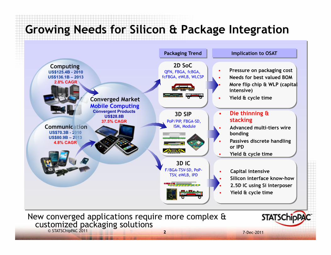
Growing Needs for Silicon & Package Integration
New converged applications require more complex & customized packaging solutions
Computing
Communication
US$125.4B - 2010 US$136.1B – 2013
2.8% CAGR
US$70.3B - 2010 US$80.9B – 2013
4.8% CAGR
Converged Market Mobile Computing
Convergent Products US$28.8B
37.5% CAGR
Packaging Trend
3D SIP PoP/PiP, FBGA-SD,
ISM, Module
3D IC F/BGA-TSV-SD, PoP-
TSV, eWLB, IPD
2D SoC QFN, FBGA, fcBGA,
fcFBGA, eWLB, WLCSP
Implication to OSAT
• Capital intensive • Silicon interface know-how • 2.5D IC using Si interposer • Yield & cycle time
• Die thinning & stacking
• Advanced multi-tiers wire bonding
• Passives discrete handling or IPD
• Yield & cycle time
• Pressure on packaging cost • Needs for best valued BOM • More flip chip & WLP (capital
intensive) • Yield & cycle time
7-Dec-2011 © STATSChipPAC 2011
3 3
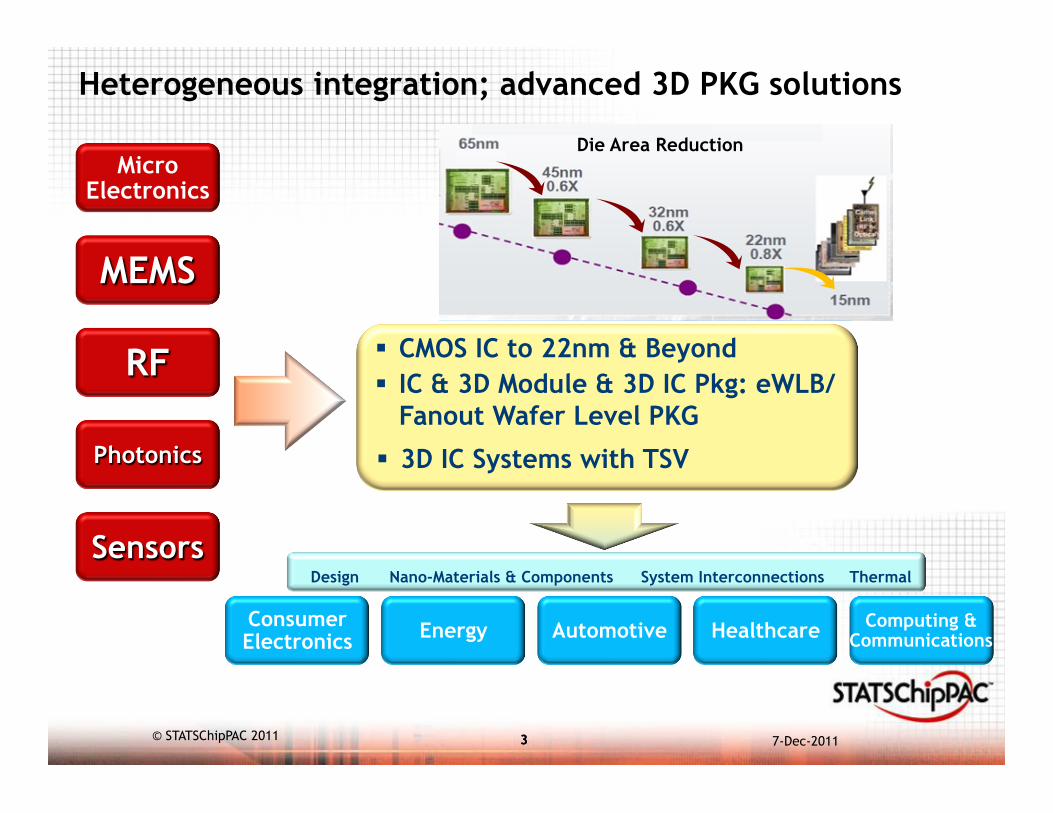
Heterogeneous integration; advanced 3D PKG solutions
Micro Electronics
MEMS
RF
Photonics
Sensors
Consumer Electronics Energy Automotive Healthcare Computing &
Communications
Design Nano-Materials & Components System Interconnections Thermal
§ CMOS IC to 22nm & Beyond § IC & 3D Module & 3D IC Pkg: eWLB/
Fanout Wafer Level PKG
§ 3D IC Systems with TSV
Die Area Reduction
7-Dec-2011 © STATSChipPAC 2011
4 4
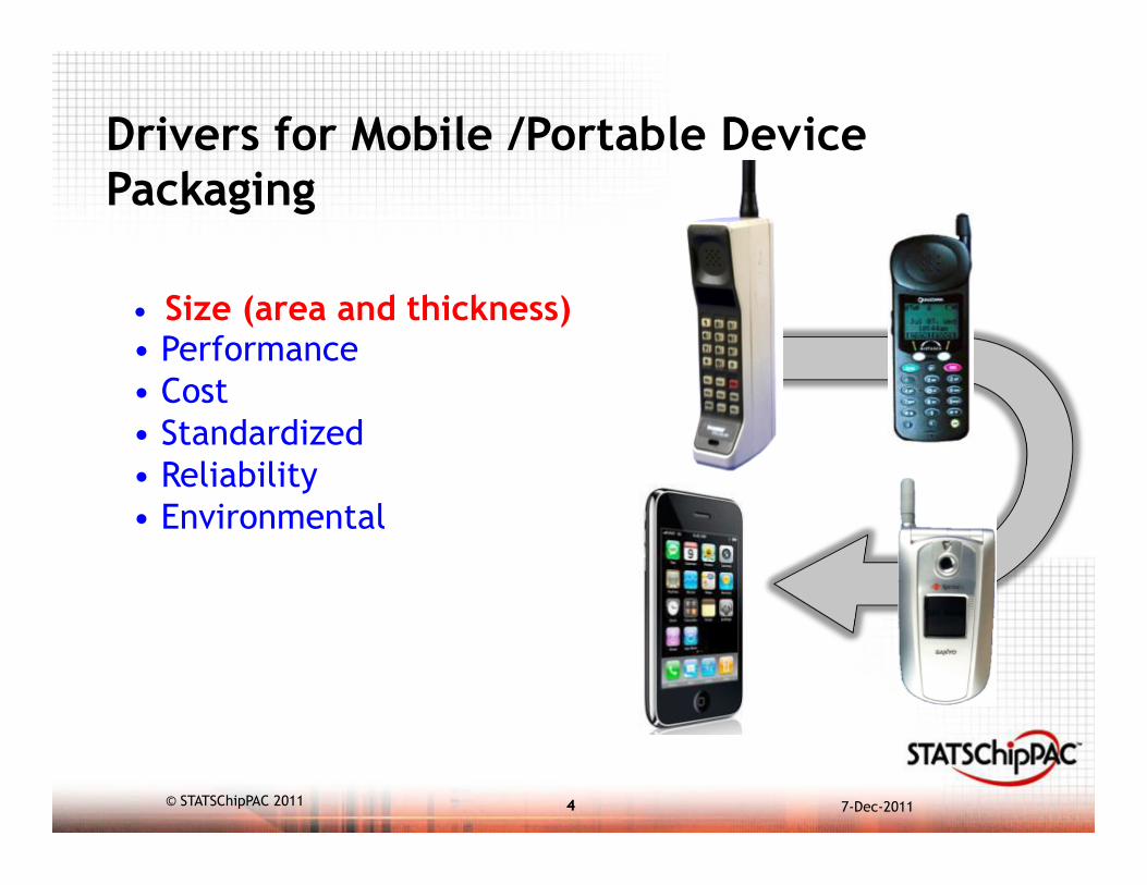
Drivers for Mobile /Portable Device Packaging
• Size (area and thickness) • Performance • Cost • Standardized • Reliability • Environmental
7-Dec-2011 © STATSChipPAC 2011
5 5
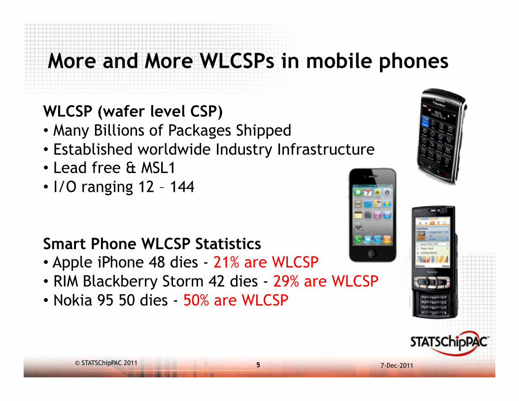
WLCSP (wafer level CSP) • Many Billions of Packages Shipped • Established worldwide Industry Infrastructure • Lead free & MSL1 • I/O ranging 12 – 144
Smart Phone WLCSP Statistics • Apple iPhone 48 dies - 21% are WLCSP • RIM Blackberry Storm 42 dies - 29% are WLCSP • Nokia 95 50 dies - 50% are WLCSP
More and More WLCSPs in mobile phones
7-Dec-2011 © STATSChipPAC 2011
6 6
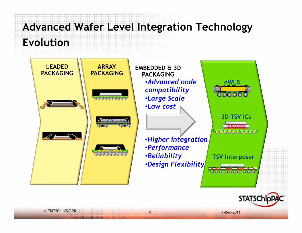
Advanced Wafer Level Integration Technology Evolution
EMBEDDED & 3D PACKAGING
3D TSV ICs
TSV Interposer
LEADED PACKAGING
ARRAY PACKAGING
eWLB • Advanced node compatibility • Large Scale • Low cost
• Higher integration • Performance • Reliability • Design Flexibility
7-Dec-2011 © STATSChipPAC 2011
7 7
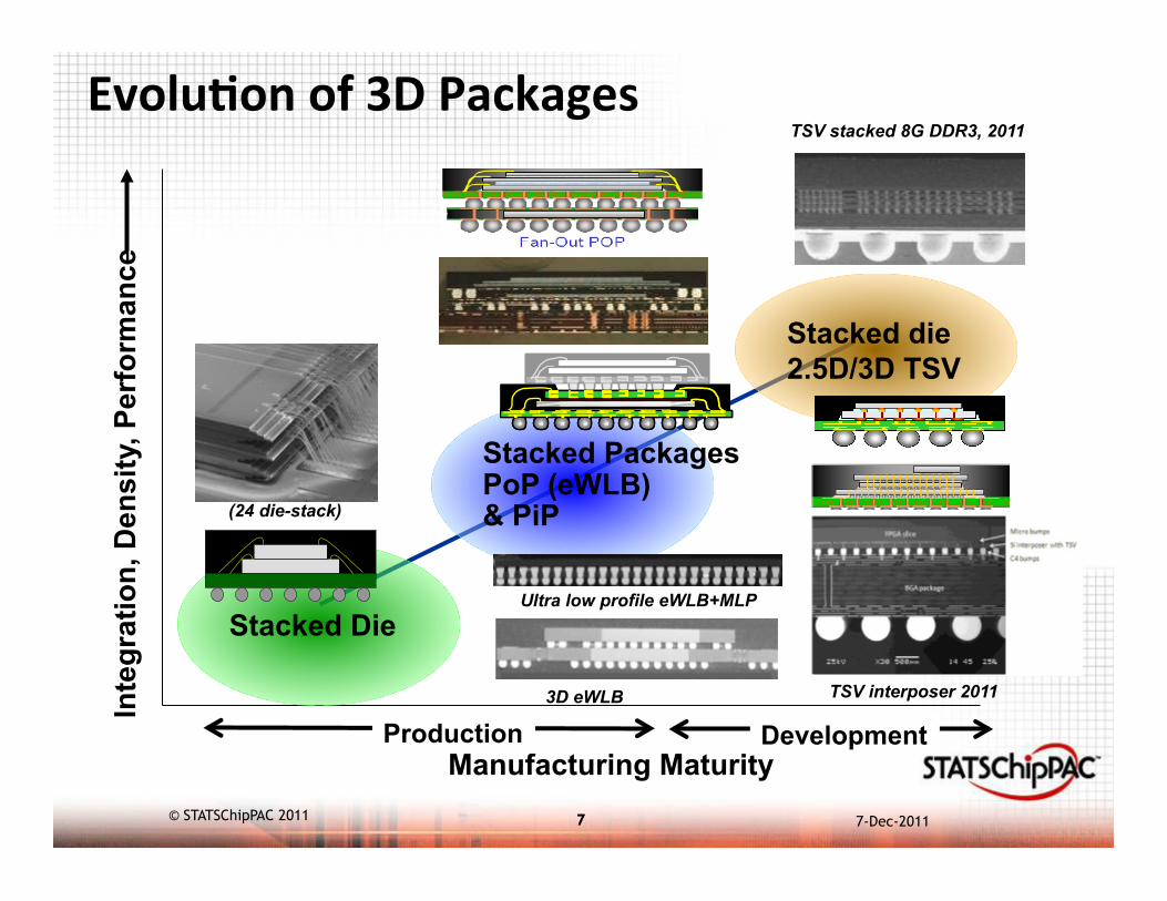
Evolu&on of 3D Packages
7
Inte
grat
ion,
Den
sity
, Per
form
ance
Manufacturing Maturity
Stacked die 2.5D/3D TSV
Stacked Die
Stacked Packages PoP (eWLB) & PiP
Production
TSV stacked 8G DDR3, 2011
(24 die-stack)
3D eWLB TSV interposer 2011
Development
Ultra low profile eWLB+MLP
7-Dec-2011 © STATSChipPAC 2011
8 8
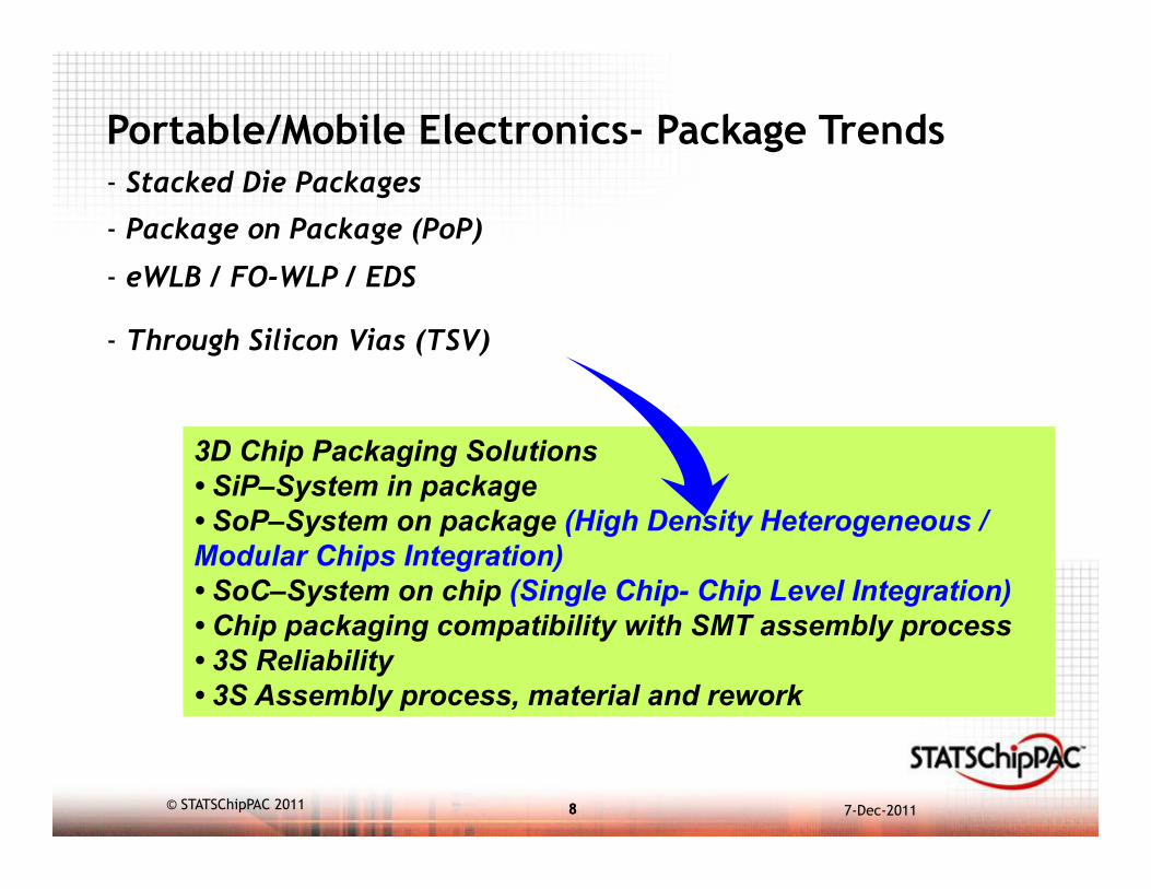
Portable/Mobile Electronics- Package Trends - Stacked Die Packages
- Package on Package (PoP)
- eWLB / FO-WLP / EDS
- Through Silicon Vias (TSV)
3D Chip Packaging Solutions • SiP–System in package • SoP–System on package (High Density Heterogeneous / Modular Chips Integration) • SoC–System on chip (Single Chip- Chip Level Integration) • Chip packaging compatibility with SMT assembly process • 3S Reliability • 3S Assembly process, material and rework
7-Dec-2011 © STATSChipPAC 2011
9 9
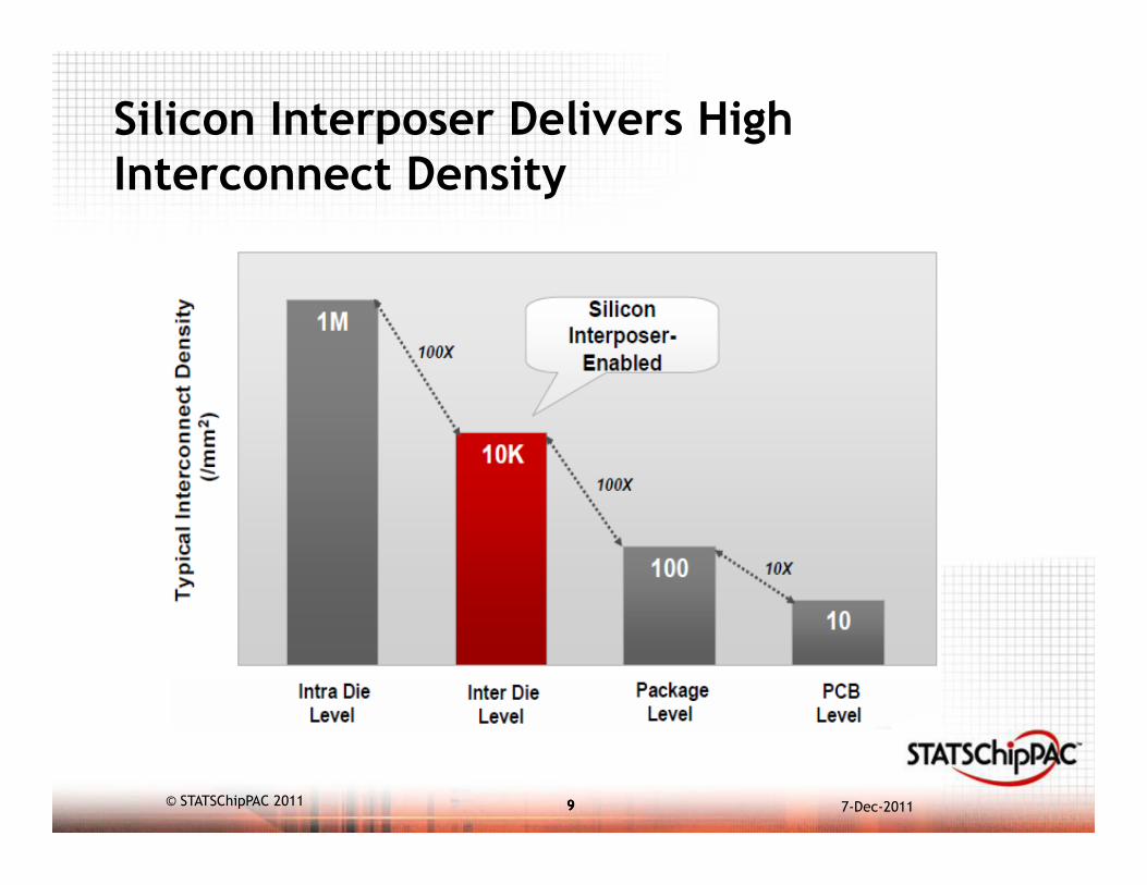
Silicon Interposer Delivers High Interconnect Density
7-Dec-2011 © STATSChipPAC 2011
10 10
eWLB and Wafer Level Packaging Technology
7-Dec-2011 © STATSChipPAC 2011
11 11
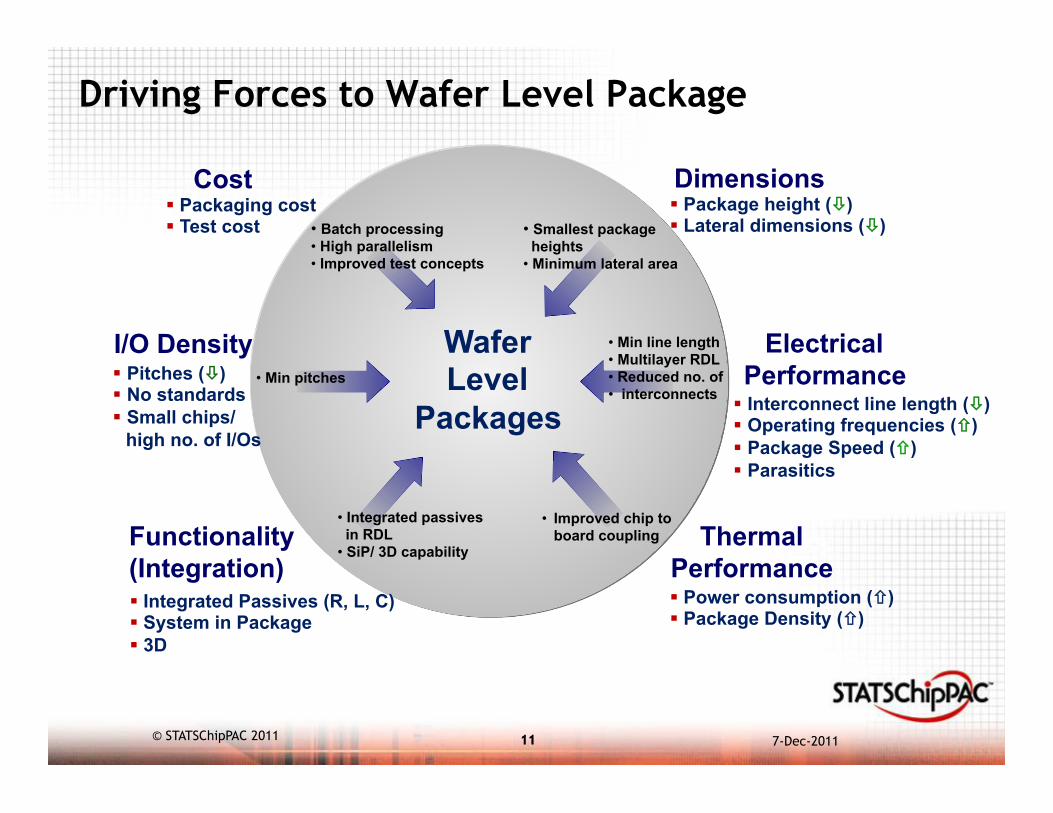
Driving Forces to Wafer Level Package
Wafer Level
Packages
§ Packaging cost § Test cost
Cost • Batch processing • High parallelism • Improved test concepts
Dimensions
• Smallest package heights • Minimum lateral area
§ Interconnect line length (ò) § Operating frequencies (ñ) § Package Speed (ñ) § Parasitics
Electrical Performance
• Min line length • Multilayer RDL • Reduced no. of • interconnects
§ Power consumption (ñ) § Package Density (ñ)
Thermal Performance
§ Integrated Passives (R, L, C) § System in Package § 3D
Functionality (Integration)
• Integrated passives in RDL • SiP/ 3D capability
§ Pitches (ò) § No standards § Small chips/ high no. of I/Os
I/O Density • Min pitches
§ Package height (ò) § Lateral dimensions (ò)
• Improved chip to board coupling
7-Dec-2011 © STATSChipPAC 2011
12 12
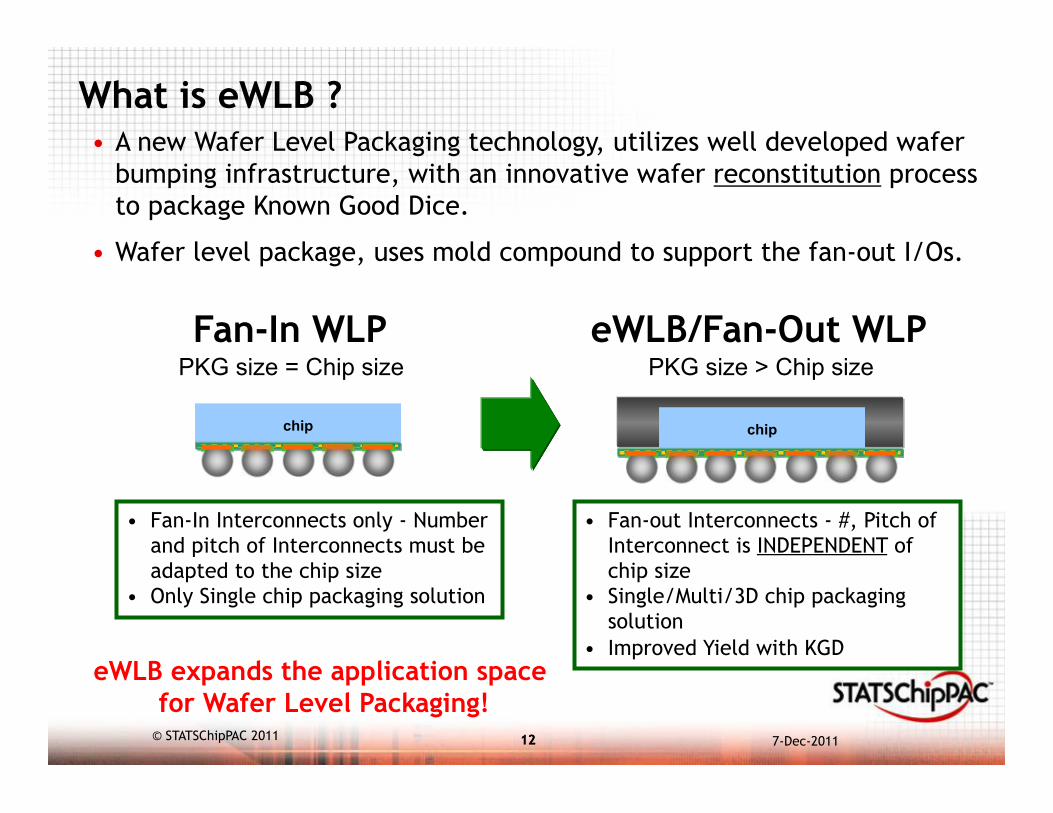
What is eWLB ? • A new Wafer Level Packaging technology, utilizes well developed wafer
bumping infrastructure, with an innovative wafer reconstitution process to package Known Good Dice.
• Wafer level package, uses mold compound to support the fan-out I/Os.
• Fan-In Interconnects only - Number and pitch of Interconnects must be adapted to the chip size
• Only Single chip packaging solution
• Fan-out Interconnects - #, Pitch of Interconnect is INDEPENDENT of chip size
• Single/Multi/3D chip packaging solution
• Improved Yield with KGD
Fan-In WLP eWLB/Fan-Out WLP PKG size = Chip size PKG size > Chip size
eWLB expands the application space for Wafer Level Packaging!
chip chip
7-Dec-2011 © STATSChipPAC 2011
13 13
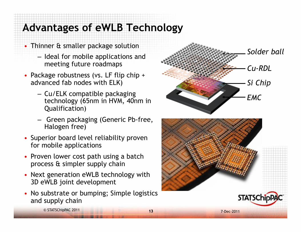
Advantages of eWLB Technology
• Thinner & smaller package solution
– Ideal for mobile applications and meeting future roadmaps
• Package robustness (vs. LF flip chip + advanced fab nodes with ELK)
– Cu/ELK compatible packaging technology (65nm in HVM, 40nm in Qualification)
– Green packaging (Generic Pb-free, Halogen free)
• Superior board level reliability proven for mobile applications
• Proven lower cost path using a batch process & simpler supply chain
• Next generation eWLB technology with 3D eWLB joint development
• No substrate or bumping; Simple logistics and supply chain
Solder ball
Cu-RDL
Si Chip
EMC
7-Dec-2011 © STATSChipPAC 2011
14 14
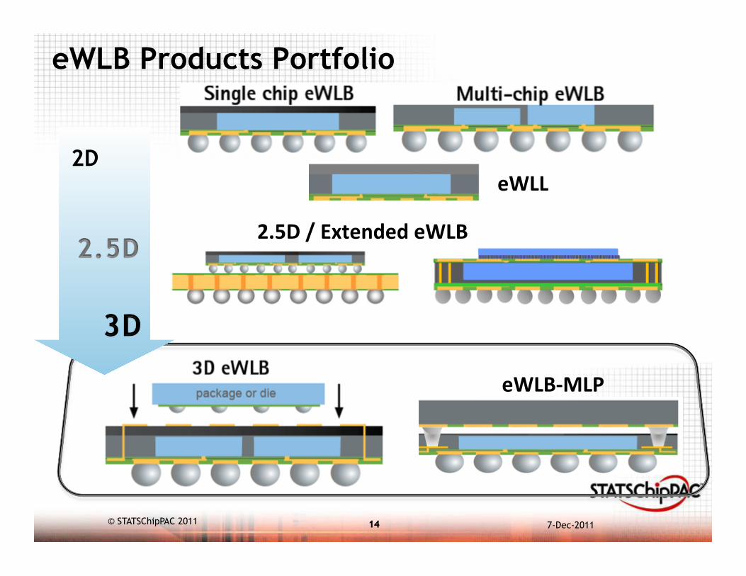
eWLB Products Portfolio
eWLB-‐MLP
2.5D / Extended eWLB
2D eWLL
7-Dec-2011 © STATSChipPAC 2011
15 15
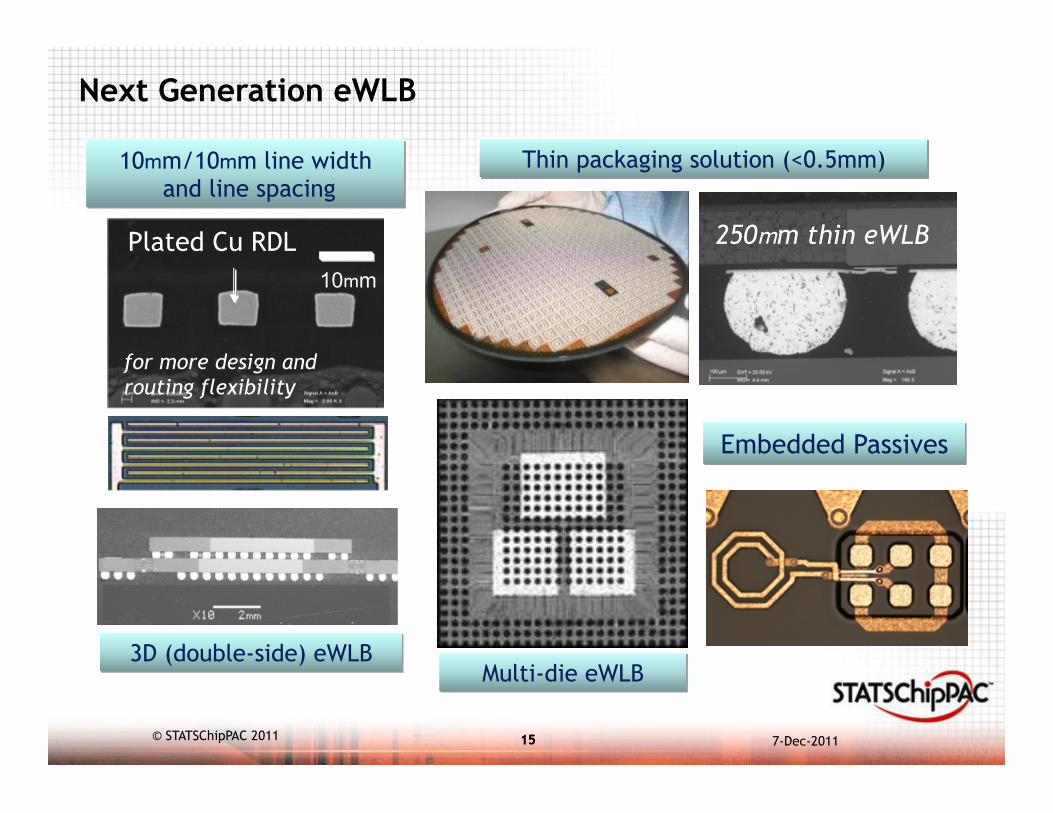
Thin packaging solution (<0.5mm)
Embedded Passives
Multi-die eWLB
Plated Cu RDL 10mm
for more design and routing flexibility
10mm/10mm line width and line spacing
3D (double-side) eWLB
250mm thin eWLB
Next Generation eWLB
7-Dec-2011 © STATSChipPAC 2011
16 16
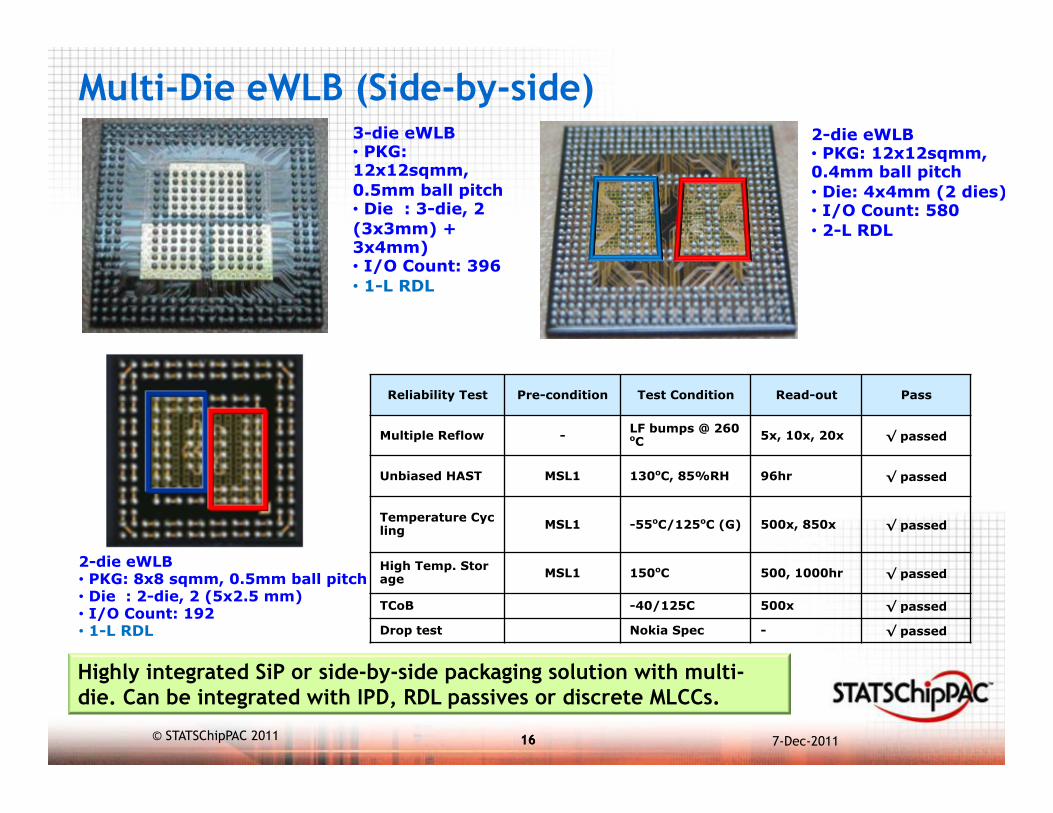
Multi-Die eWLB (Side-by-side) 2-die eWLB • PKG: 12x12sqmm, 0.4mm ball pitch • Die: 4x4mm (2 dies) • I/O Count: 580 • 2-L RDL
3-die eWLB • PKG: 12x12sqmm, 0.5mm ball pitch • Die : 3-die, 2 (3x3mm) + 3x4mm) • I/O Count: 396 • 1-L RDL
Reliability Test Pre-condition Test Condition Read-out Pass
Multiple Reflow - LF bumps @ 260oC 5x, 10x, 20x √ passed
Unbiased HAST MSL1 130oC, 85%RH 96hr √ passed
Temperature Cycling MSL1 -55oC/125oC (G) 500x, 850x √ passed
High Temp. Storage MSL1 150oC 500, 1000hr √ passed
TCoB -40/125C 500x √ passed
Drop test Nokia Spec - √ passed
Highly integrated SiP or side-by-side packaging solution with multi-die. Can be integrated with IPD, RDL passives or discrete MLCCs.
2-die eWLB • PKG: 8x8 sqmm, 0.5mm ball pitch • Die : 2-die, 2 (5x2.5 mm) • I/O Count: 192 • 1-L RDL
7-Dec-2011 © STATSChipPAC 2011
17 17
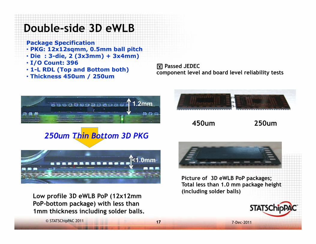
Double-side 3D eWLB Package Specification • PKG: 12x12sqmm, 0.5mm ball pitch • Die : 3-die, 2 (3x3mm) + 3x4mm) • I/O Count: 396 • 1-L RDL (Top and Bottom both) • Thickness 450um / 250um
450um 250um
Low profile 3D eWLB PoP (12x12mm PoP-bottom package) with less than 1mm thickness including solder balls.
1.2mm
<1.0mm
250um Thin Bottom 3D PKG
Picture of 3D eWLB PoP packages; Total less than 1.0 mm package height (including solder balls)
Passed JEDEC component level and board level reliability tests
7-Dec-2011 © STATSChipPAC 2011
18 18
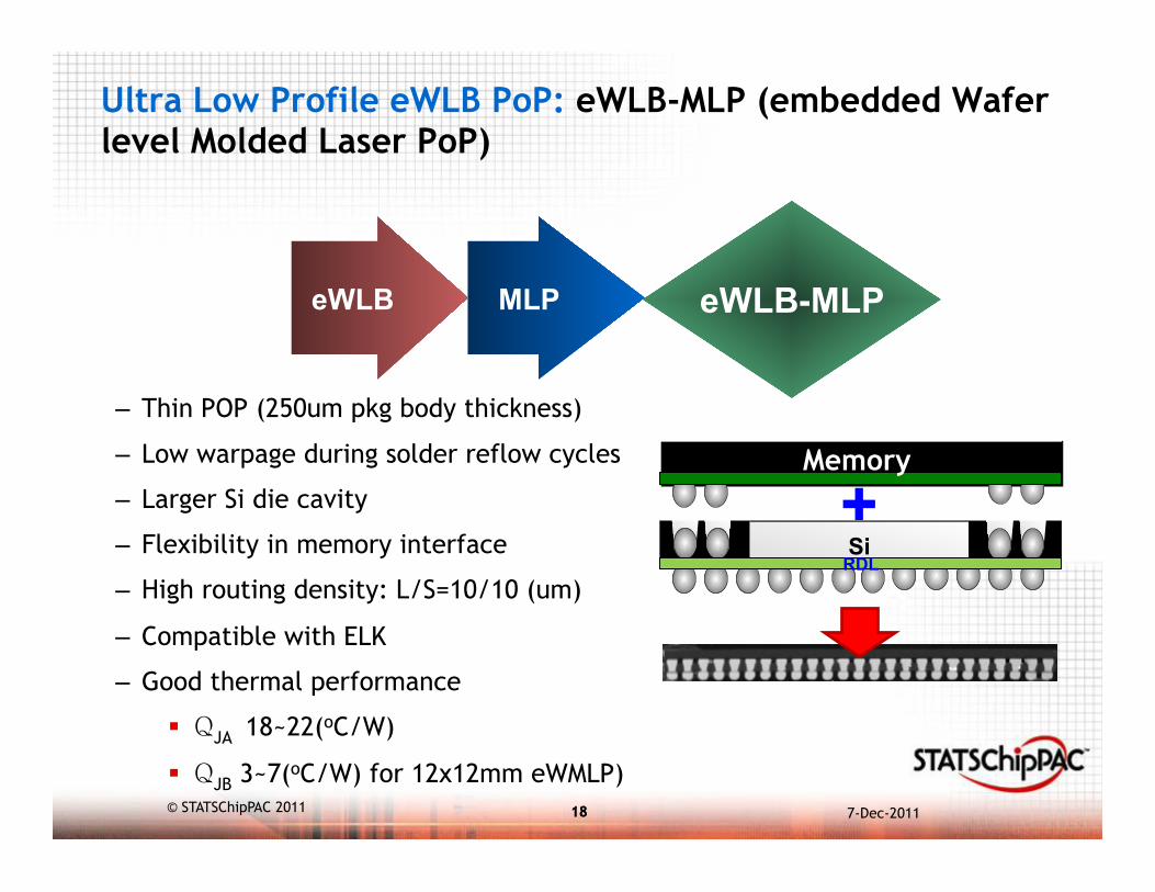
Ultra Low Profile eWLB PoP: eWLB-MLP (embedded Wafer level Molded Laser PoP)
– Thin POP (250um pkg body thickness)
– Low warpage during solder reflow cycles
– Larger Si die cavity
– Flexibility in memory interface
– High routing density: L/S=10/10 (um)
– Compatible with ELK
– Good thermal performance
§ QJA 18~22(oC/W)
§ QJB 3~7(oC/W) for 12x12mm eWMLP)
Si RDL
MLP eWLB
eWLB-MLP
+Memory
7-Dec-2011 © STATSChipPAC 2011
19 19
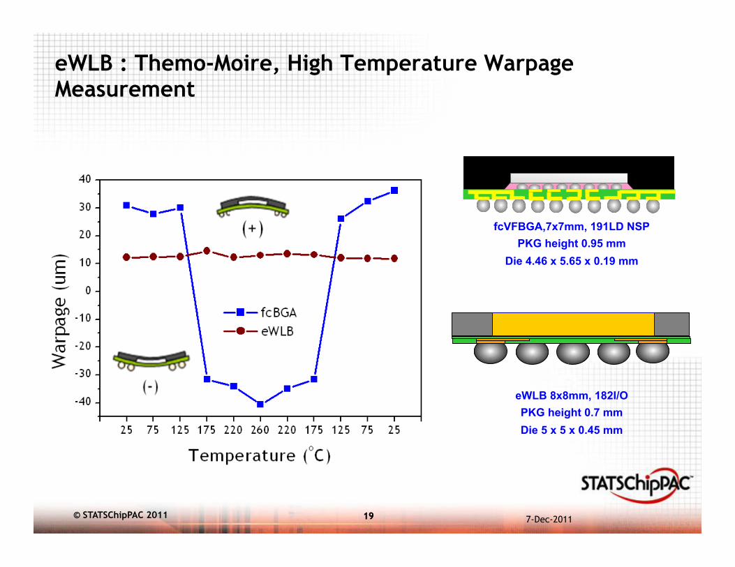
eWLB : Themo-Moire, High Temperature Warpage Measurement
fcVFBGA,7x7mm, 191LD NSP
PKG height 0.95 mm Die 4.46 x 5.65 x 0.19 mm
eWLB 8x8mm, 182I/O
PKG height 0.7 mm Die 5 x 5 x 0.45 mm
7-Dec-2011 © STATSChipPAC 2011
20 20
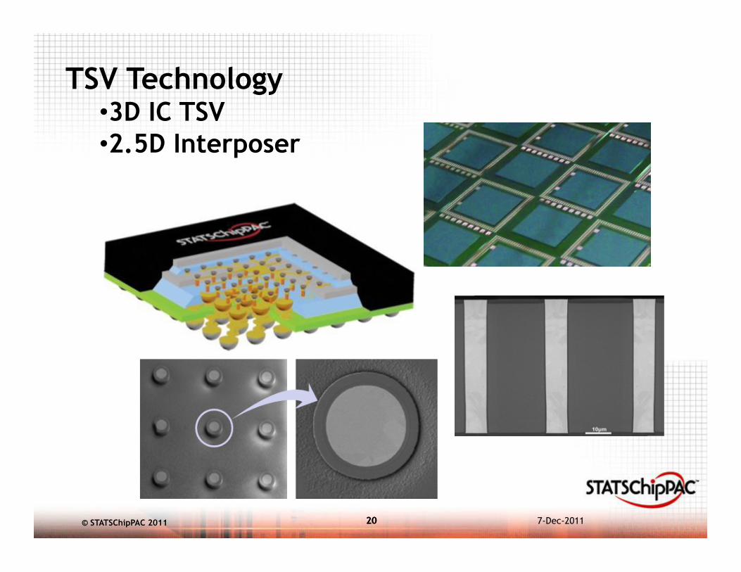
TSV Technology • 3D IC TSV • 2.5D Interposer
7-Dec-2011 © STATSChipPAC 2011
21 21
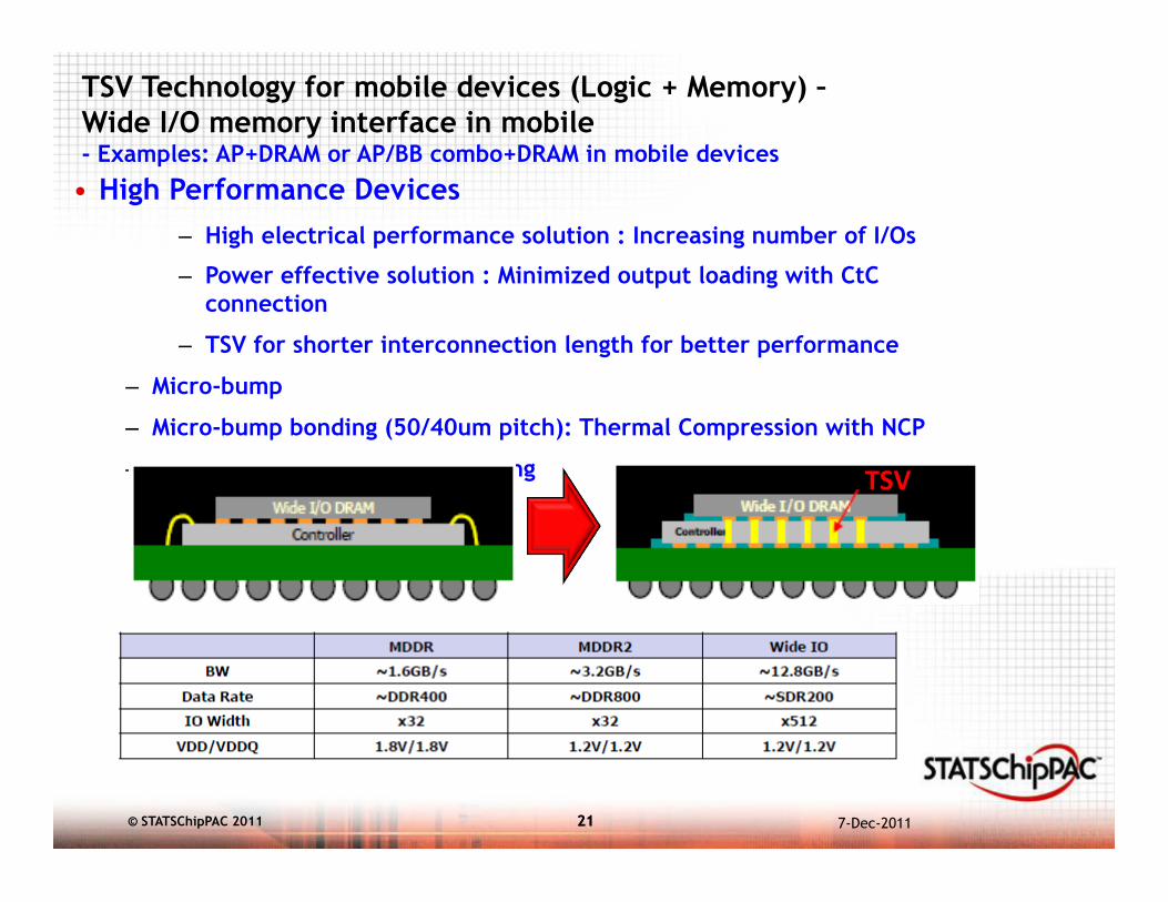
TSV Technology for mobile devices (Logic + Memory) – Wide I/O memory interface in mobile - Examples: AP+DRAM or AP/BB combo+DRAM in mobile devices
• High Performance Devices – High electrical performance solution : Increasing number of I/Os
– Power effective solution : Minimized output loading with CtC connection
– TSV for shorter interconnection length for better performance
– Micro-bump
– Micro-bump bonding (50/40um pitch): Thermal Compression with NCP
– Thin wafer handling and packaging TSV
7-Dec-2011 © STATSChipPAC 2011
22 22
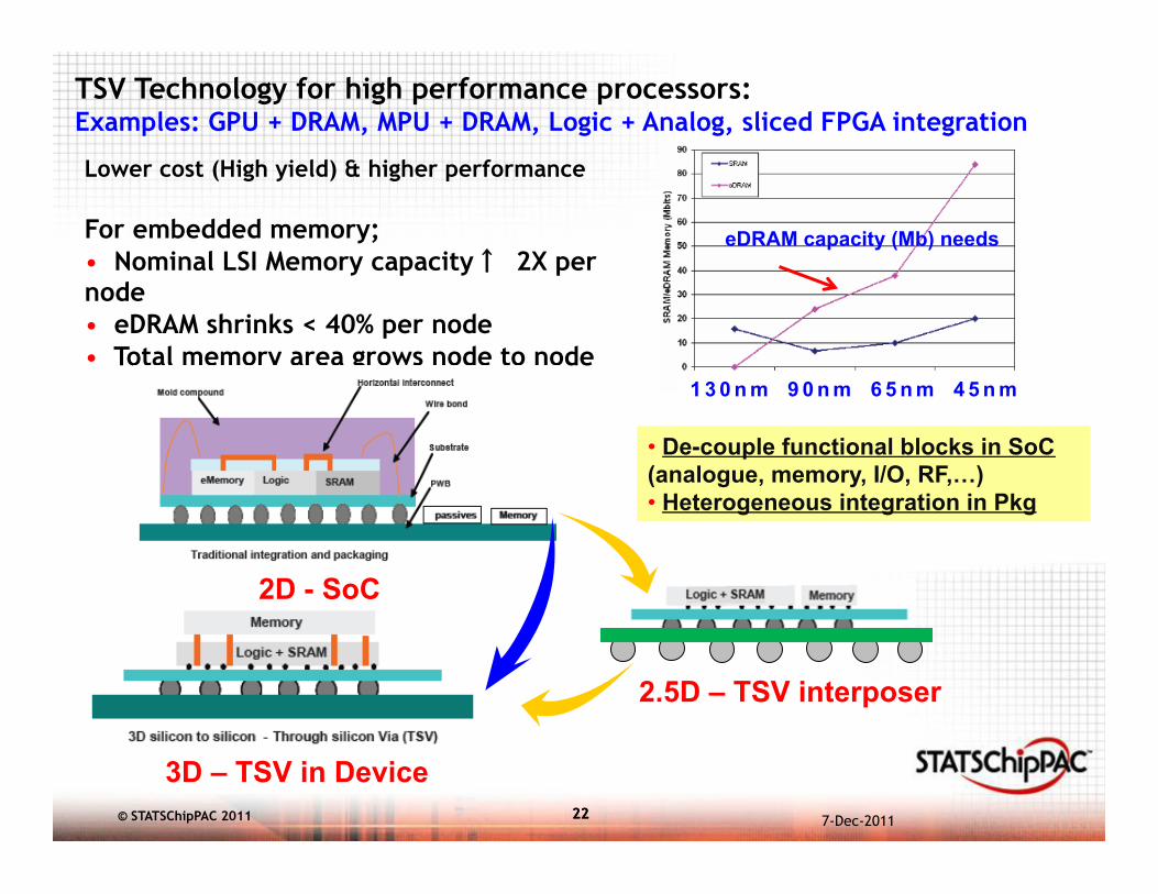
Lower cost (High yield) & higher performance For embedded memory; • Nominal LSI Memory capacity↑ 2X per node • eDRAM shrinks < 40% per node • Total memory area grows node to node
• De-couple functional blocks in SoC (analogue, memory, I/O, RF,…) • Heterogeneous integration in Pkg
TSV Technology for high performance processors: Examples: GPU + DRAM, MPU + DRAM, Logic + Analog, sliced FPGA integration
2D - SoC
2.5D – TSV interposer
3D – TSV in Device
eDRAM capacity (Mb) needs
1 3 0 n m 9 0 n m 6 5 n m 4 5 n m
7-Dec-2011 © STATSChipPAC 2011
23 23
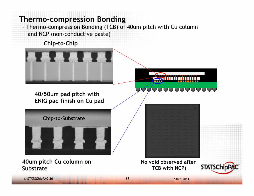
No void observed after TCB with NCP)
40/50um pad pitch with ENIG pad finish on Cu pad
Chip-to-Substrate
Chip-to-Chip
40um pitch Cu column on Substrate
Thermo-compression Bonding – Thermo-compression Bonding (TCB) of 40um pitch with Cu column and NCP (non-conductive paste)
7-Dec-2011 © STATSChipPAC 2011
24 24
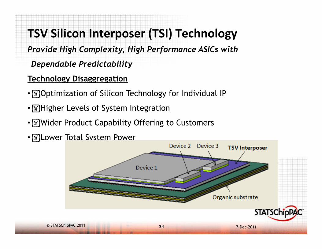
TSV Silicon Interposer (TSI) Technology Provide High Complexity, High Performance ASICs with
Dependable Predictability
Technology Disaggregation
• Optimization of Silicon Technology for Individual IP
• Higher Levels of System Integration
• Wider Product Capability Offering to Customers
• Lower Total System Power
7-Dec-2011 © STATSChipPAC 2011
25 25
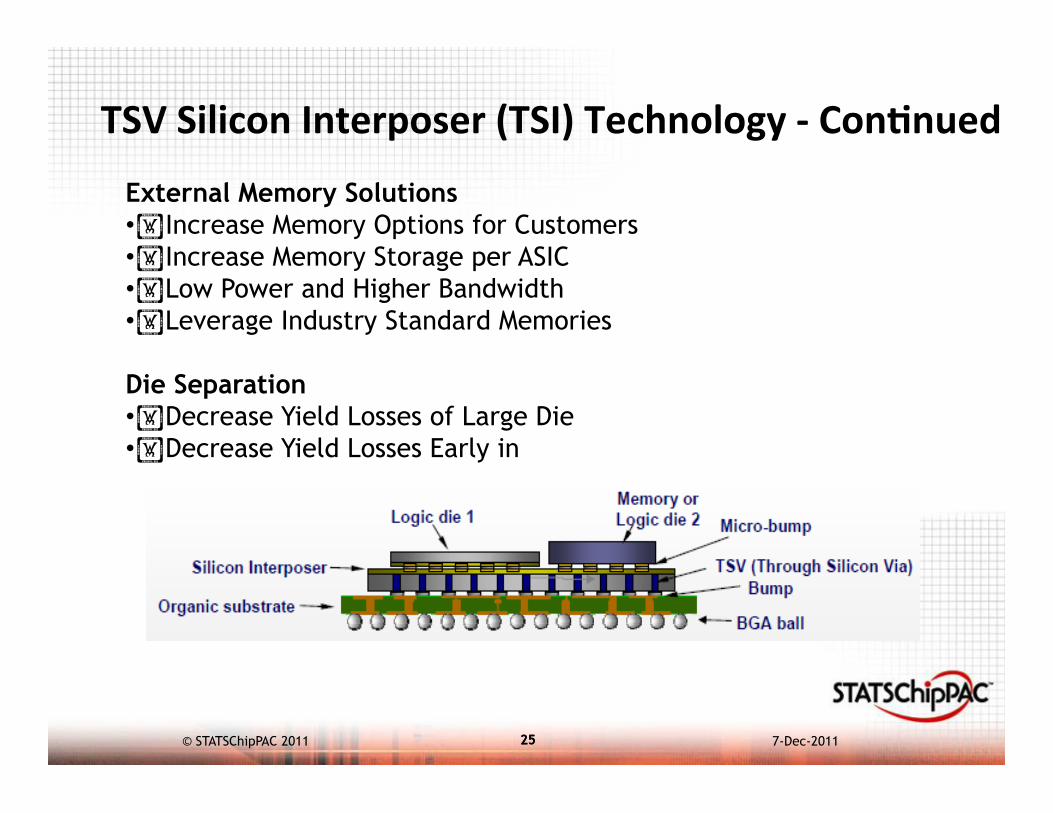
External Memory Solutions • Increase Memory Options for Customers • Increase Memory Storage per ASIC • Low Power and Higher Bandwidth • Leverage Industry Standard Memories Die Separation • Decrease Yield Losses of Large Die • Decrease Yield Losses Early in
TSV Silicon Interposer (TSI) Technology -‐ Con&nued
7-Dec-2011 © STATSChipPAC 2011
26 26
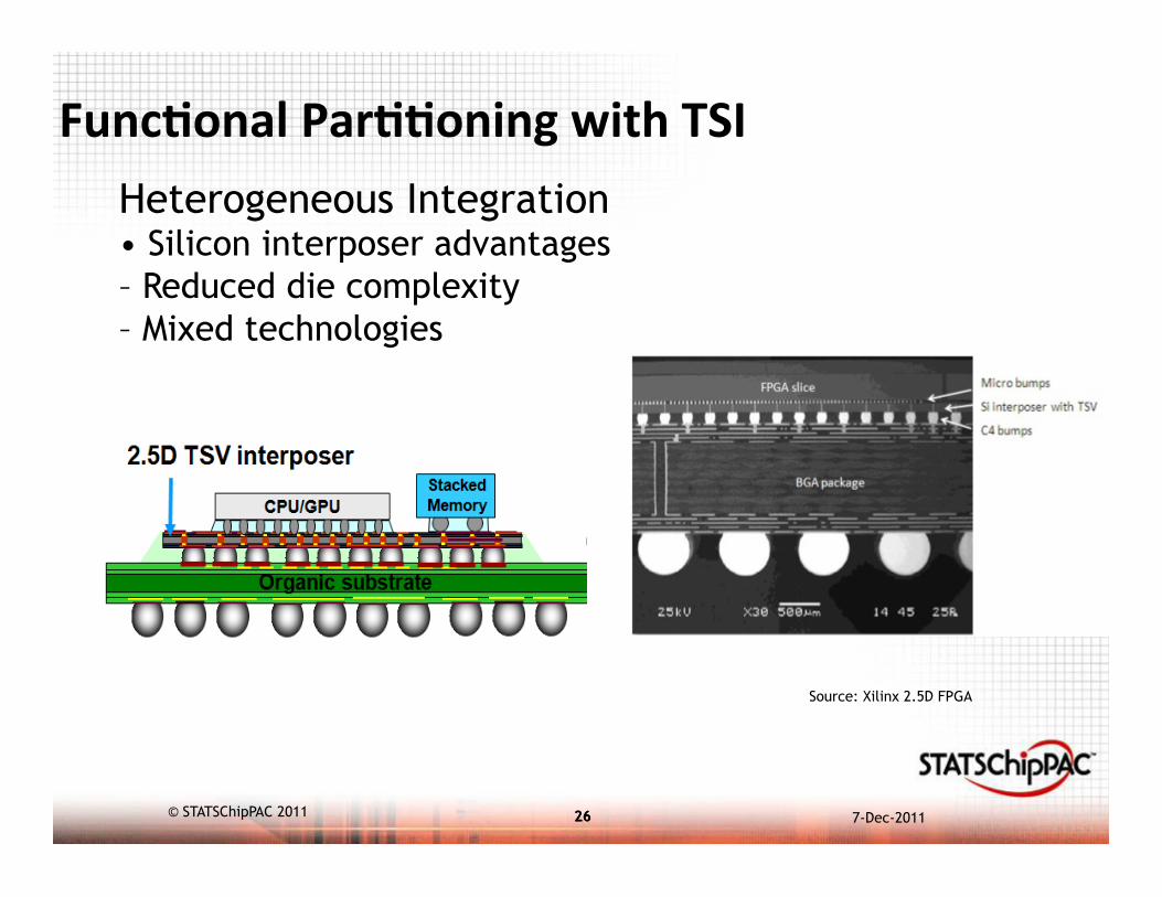
Func&onal Par&&oning with TSI Heterogeneous Integration • Silicon interposer advantages – Reduced die complexity – Mixed technologies
Source: Xilinx 2.5D FPGA
7-Dec-2011 © STATSChipPAC 2011
27 27
• 3D especially with TSVs is a revolutionary change requiring significant infrastructure additions.
• 2.5D allows use of mixed interconnect ICs from different sources and is evolutionary.
• 2.5D may become as essential within a package assembly as underfill epoxy for both single chips and stacked 3D chips.
• 2.5D is not limited to silicon – glass and even organic solutions provide economical benefits in applications where silicon is inappropriate.
2.5D and 3D will Coexist ?
7-Dec-2011 © STATSChipPAC 2011
28 28
Summary • Wafer level packaging is a key technology enabler for future
heterogeneous integration.
• Next generation and 3D eWLBs would be a good solution for future needs in mobile/portable applications, such as PoP and 3D SiP.
• With scale-up and higher throughput, large panel approach is next step for further market-penentration as cost-effective packaging solutions.
• TSV technology is critical for continued evolution of semiconductor industry. TSV interposer technology is one of early application of TSV technology.
• As with all new technologies for 2.5D/3D TSV wafer level integration; Product applications & drivers are critical.
• Alternative technology, eWLB technology, wafer level packaging solution enabling 3D wafer level integration with low cost solution.
• More collaborative cost/ performance analysis across FE-BE FAB, EDA, Assembly, Reliability, Metrology & Test are needed for successful TSV biz establishment.
7-Dec-2011 © STATSChipPAC 2011
29 29
Thank You
7-Dec-2011 © STATSChipPAC 2011