advanced technologies for brain-inspired computingadvanced technologies for brain-inspired computing...
TRANSCRIPT

&
www.cea.fr
Advanced Technologies for Brain -Inspired
Computing
Fabien CLERMIDY*
Rodolphe Heliot*, Alexandre Valentian*,
Christian Gamrat**, Olivier Bichler**, Marc
Duranton**, Bilel Blehadj# and Olivier
Temam#
.
*CEA-Leti, Grenoble, France **CEA-List, Paris, France
# INRIA, Paris, France
Cliquez pour modifier le style du titre
ASPDAC –24th January 2014 | 2
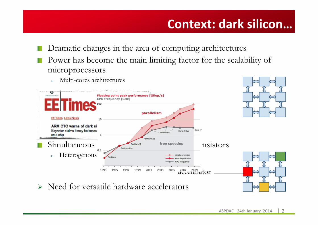
Context: dark silicon…
Dramatic changes in the area of computing architectures
Power has become the main limiting factor for the scalability of microprocessors
� Multi-cores architectures
Simultaneous use of a limited number of transistors� Heterogenous multi-cores
� Need for versatile hardware accelerators
accelerator

Cliquez pour modifier le style du titre
ASPDAC –24th January 2014 | 3
…and variability
Dramatic changes in the area of computing architectures
Robustness issues
� Robust accelerators
(Borkar 2005)

Cliquez pour modifier le style du titre
ASPDAC –24th January 2014 | 4
for new applications
Today : scientific computing, cryptography, …
Tomorrow : data Recognition, Mining, Synthesis

Cliquez pour modifier le style du titre
ASPDAC –24th January 2014 | 5
A potential answer : Neural networks
Neural Networks are good candidates
They provide Robustness
Good application scope
But classically limited by 2D hardware
solutions
� Limited interconnections, costly long range ones
� But the HW situation has changed !
Optimization
ClassificationClustering
Approximation
Prediction
Signal processing
Cliquez pour modifier le style du titre
ASPDAC –24th January 2014 | 6
• Context
• Exploiting resistive memories
• Analogue neurons and 3D-TSV
• Towards monolithic 3D…
• Conclusion
Outline

Cliquez pour modifier le style du titre
ASPDAC –24th January 2014 | 7
Volatile Memory
Polarizationchange
Charge Trap Resistance Change = memristorsDRAMSRAM
SONOSFLASH FRAMRRAM
Resistancechanges
Phasedependent Resistance changes
1
2’
2
V1V0
1’ “0””
I
oxide
1
2’
2
V1V0
1’ “0””
I 1
2’
2
V1V0
1’ “0””
I
oxide
Interface or bulk Resistance changes
Current -based Programming & Reading
MRAMPRAM
Non-Volatile Memory
MagnetoCharge -based Programming & Reading
New memory technologies

Cliquez pour modifier le style du titre
ASPDAC –24th January 2014 | 8
Memristors
DRAM FLASH MRAM PRAM RRAM
Nand STT OxRAM CBRAM
Compatibility
with CMOS - - - - + + + + +Scalability 32nm 15nm 20-30nm 10-20 nm 10 nm 10-20 nm
Density 6-8f2 4f2 35-40f2 4-6f2 4-6f2 4-6f2
Maturity + + + + - - - - - -Byte @ YES NO YES YES YES YES
Writing cycle 50ns 0.1 ms 20ns 100 ns 150 ns 1-10 us
Endurance 1,00E+16 1,00E+05 1,00E+15 1,00E+09 →1,00E+06 1,00E+06
Plus Perf. NV
Perf. + NV +
Endurance
Perf. + NV+
density
Perf. + NV+
density
Vitesse lect+
NV+ densité
Minus Scalability
Endurance
Perf - -
Costly tech.
Delay wrt
CMOS nodes
consumptio
n
Endurance,
Forming
Endurance,
Perf.

Cliquez pour modifier le style du titre
ASPDAC –24th January 2014 | 9
Memristor as a Synapse
Concept introduced by Chua
“Memristor-The missing circuit element” - 1971
Strukov & Snider developed it
“The missing memristor found” - Nature 2008
“Spike-timing-dependent learning in memristive
nanodevices” – Nanoarch 2008
Concept “memristor = synapse weight”
So easy ? u1
u2
s=u1+u2
w=1
w=1

Cliquez pour modifier le style du titre
ASPDAC –24th January 2014 | 10
Crossbar of Synapses
Require “gradually” programming memristorsDifficulty is to obtain equivalent potentiation / depression phases
D. Querlioz, et al. “Immunity to Device Variations in a Spiking Neural Network with MemristiveNanodevices,” IEEE TNANO 2013

Cliquez pour modifier le style du titre
ASPDAC –24th January 2014 | 11
Phase-Change Memories
Material with 2 stable phasesChalcogenide alloys : GST, GeTe, …
Hysteresis cycle between 2 states
Transition by Joule heating
Polycrystal Amorphous
High conductivity Low conductivity
Reversible
Phase Change
Amorphous
tQUENCH < 10 ns
Tmelt
Polycrystal
tQUENCH > 100 ns
TX

Cliquez pour modifier le style du titre
ASPDAC –24th January 2014 | 12
A solution: 2-PCM Synapse
Symmetric Long-Term-Potentiation and Long-Term
depression behavior by using pulsed crystallization.

Cliquez pour modifier le style du titre
ASPDAC –24th January 2014 | 13
• Context
• Exploiting resistive memories
• Analogue neurons and 3D -TSV
• Towards monolithic 3D…
• Conclusion
Outline

Cliquez pour modifier le style du titre
ASPDAC –24th January 2014 | 14
Analogue neurons
Compact design (5x gain vs digital)
Low power consumption (20x gain vs digital)
Ability to interface sensors directly with the
processing part
Computational efficiency
Leaky Integrate and Fire Neuron in CMOS 65nm
accept spikes in 1kHz-1 Mhz range
Drawback:
Large capacitance
required (0,5-1pF)
⇒MIM
⇒ Large area (not
scalable !)
A. Joubert et al. “A robust and compact 65 nm LIF analog neuron for computational purposes,” IEEE NEWCAS 2011

Cliquez pour modifier le style du titre
ASPDAC –24th January 2014 | 15
Through Silicon Vias
Used for crossing circuits in 3D stacking
Present large “parasitic” capacitance
Demonstrated feasibility
A. Joubert et al., “Capacitance of TSVs in 3-D stacked chips a problem? Not for neuromorphicsystems”, DAC’12

Cliquez pour modifier le style du titre
ASPDAC –24th January 2014 | 16
3D integration using TSV
(a)
(d)
(b)
(c)
Threshold
W. InjectionCapacitance
Back end
TSV
Chip 1
Chip 2
Front end
(a) Standard 2D
neuromorphic architecture
(b) 3D stacking with
standard 2D neurons
(c) et (d) 3D stacking
with TSV-based neurons
Chaabouni et. al. (2010)

Cliquez pour modifier le style du titre
ASPDAC –24th January 2014 | 17
• Context
• Exploiting resistive memories
• Analogue neurons and 3D-TSV
• Towards monolithic 3D…
• Conclusion
Outline

Cliquez pour modifier le style du titre
ASPDAC –24th January 2014 | 18
Brain is 3D !
• 3D technologies
• Parallel IntegrationDies fabricated separately then vertically stacked, such as:
�Through-Silicon-Via (TSV)
�Copper-to-Copper (Cu-Cu) contact
�High-Density TSVs
• Sequential IntegrationSecond transistor layer is fabricated directly on the top of first one.(Cold process)
� 3D Monolithic Integration (3DMI)
Interposer
TSV (~10um)
Cu-Cu (~3um)
3D
ve
rtic
al
inte
rco
nn
ect
s d
iam
ete
r3
D v
ert
ica
l in
terc
on
ne
cts
dia
me
terLow-density TSV (~50 µm)
TSV (~5-10µm)
HD-TSV (~ 1µm)
Cu-Cu (~ 1µm)
3D
ve
rtic
al
inte
rco
nn
ect
s d
iam
ete
r3
D v
ert
ica
l in
terc
on
ne
cts
dia
me
ter
3D MI(~100nm)

Cliquez pour modifier le style du titre
ASPDAC –24th January 2014 | 19
Monolithic 3D
Integration is monolithic using a “cold” process
Allows 100 nm 3D vias pitch
=> Open perspectives for real 3D implementation
P. Batude et al., "GeOI and SOI 3D Monolithic Cell integrations for High Density Applications" VLSIT 2009

Cliquez pour modifier le style du titre
ASPDAC –24th January 2014 | 20
2D versus 3D mapping on NN
Using 3D TSV allows a “cube” of neurons
Drastically reduce interconnects
Example shown here is 3x more efficient in 3D
184 neurons with 1181 connections
2-D 3-D

Cliquez pour modifier le style du titre
ASPDAC –24th January 2014 | 21
Conclusion
Neuromorphic architectures are appealingSolve dark silicon issues
Adapted to modern applications
And can take benefit of advances technologiesSynapse => Memristors = RRAM, PCM
Neurons => Analogue neurons + high-capacitance TSV
Interconnections => high-density 3D
The path is open for the next neuromorphic
revolution!

Centre de Grenoble
17 rue des Martyrs
38054 Grenoble Cedex
Centre de Saclay
Nano-Innov PC 172
91191 Gif sur Yvette Cedex
Questions ?