agilent j-bert m8020a high-performance bert · agilent j-bert m8020a high-performance bert ......
TRANSCRIPT
Agilent J-BERT M8020A High-Performance BERT
Master Your Next Designs
Preliminary Data Sheet Version 0.8
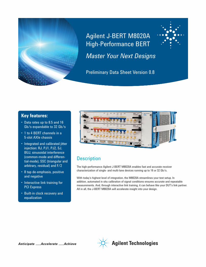
DescriptionThe high-performance Agilent J-BERT M8020A enables fast and accurate receiver characterization of single- and multi-lane devices running up to 16 or 32 Gb/s. With today’s highest level of integration, the M8020A streamlines your test setup. In addition, automated in situ calibration of signal conditions ensures accurate and repeatable measurements. And, through interactive link training, it can behave like your DUT’s link partner. All in all, the J-BERT M8020A will accelerate insight into your design.
Key features:• Data rates up to 8.5 and 16
Gb/s expandable to 32 Gb/s• 1 to 4 BERT channels in a
5-slot AXIe chassis • Integrated and calibrated jitter
injection: RJ, PJ1, PJ2, SJ, BUJ, sinusoidal interference (common-mode and differen-tial-mode), SSC (triangular and arbitrary, residual) and F/2
• 8 tap de-emphasis, positive and negative
• Interactive link training for PCI Express
• Built-in clock recovery and equalization
2
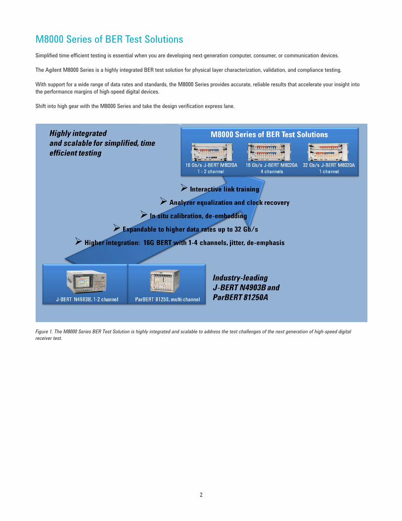
M8000 Series of BER Test SolutionsSimplified time-efficient testing is essential when you are developing next-generation computer, consumer, or communication devices.
The Agilent M8000 Series is a highly integrated BER test solution for physical layer characterization, validation, and compliance testing.
With support for a wide range of data rates and standards, the M8000 Series provides accurate, reliable results that accelerate your insight into the performance margins of high-speed digital devices.
Shift into high gear with the M8000 Series and take the design verification express lane.
Figure 1. The M8000 Series BER Test Solution is highly integrated and scalable to address the test challenges of the next generation of high-speed digital receiver test.
3
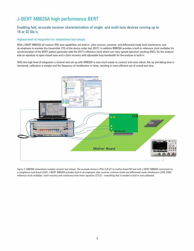
J-BERT M8020A high-performance BERTEnabling fast, accurate receiver characterization of single- and multi-lane devices running up to 16 or 32 Gb/s.
Highest level of integration for streamlined test setupsWith J-BERT M8020A all receiver (RX) test capabilities are built-in: jitter sources, common- and differential-mode level interference, and de-emphasis to emulate the transmitter (TX) of the device under test (DUT). In addition M8020A provides a built-in reference clock multiplier for synchronization of the BERT pattern generator with the DUT’s reference clock which can carry spread spectrum clocking (SSC). On the analyzer side an equalizer to open closed eyes and a clock recovery with adjustable loop bandwidth for the analyzer is built-in.
With this high level of integration a receiver test set-up with M8020A is now much easier to connect and more robust. Set up and debug time is shortened, calibration is simpler and the frequency of recalibration is lower, resulting in more efficient use of overall test time.
Figure 2: M8020A streamlines complex receiver test setups. The example shows a PCIe 3 (8 GT/s) mother board RX test with J-BERT M8020A connected via a compliance load board (CLB). J-BERT M8020A provides built-in de-emphasis, jitter sources, common-mode and differential mode interference (CMI, DMI), reference clock multiplier, clock recovery and continuous time linear equalizer (CTLE) – everything that is needed is built-in and calibrated.
4
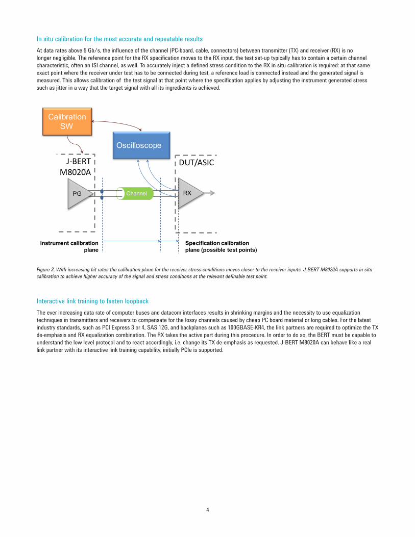
In situ calibration for the most accurate and repeatable resultsAt data rates above 5 Gb/s, the influence of the channel (PC-board, cable, connectors) between transmitter (TX) and receiver (RX) is no longer negligible. The reference point for the RX specification moves to the RX input, the test set-up typically has to contain a certain channel characteristic, often an ISI channel, as well. To accurately inject a defined stress condition to the RX in situ calibration is required: at that same exact point where the receiver under test has to be connected during test, a reference load is connected instead and the generated signal is measured. This allows calibration of the test signal at that point where the specification applies by adjusting the instrument generated stress such as jitter in a way that the target signal with all its ingredients is achieved.
Interactive link training to fasten loopbackThe ever increasing data rate of computer buses and datacom interfaces results in shrinking margins and the necessity to use equalization techniques in transmitters and receivers to compensate for the lossy channels caused by cheap PC board material or long cables. For the latest industry standards, such as PCI Express 3 or 4, SAS 12G, and backplanes such as 100GBASE-KR4, the link partners are required to optimize the TX de-emphasis and RX equalization combination. The RX takes the active part during this procedure. In order to do so, the BERT must be capable to understand the low level protocol and to react accordingly, i.e. change its TX de-emphasis as requested. J-BERT M8020A can behave like a real link partner with its interactive link training capability, initially PCIe is supported.
Figure 3. With increasing bit rates the calibration plane for the receiver stress conditions moves closer to the receiver inputs. J-BERT M8020A supports in situ calibration to achieve higher accuracy of the signal and stress conditions at the relevant definable test point.
Channel RX
Instrument calibrationplane
PG
J-BERTM8020A
DUT/ASICIC
Specification calibrationplane (possible test points)
Oscilloscope
Calibration SW
5
ApplicationsR&D and test engineers who characterize and verify compliance of chips, devices, boards and systems with serial I/O ports up to 16 Gb/s. The M8020A can be used to test popular serial bus standards, such as PCI Express®, SATA/SAS, DisplayPort, USB Super Speed, MIPI M-PHY, SD UHS-II, Fibre Channel, QPI, memory buses, backplanes, repeaters, active optical cables, Thunderbolt, 10 GbE/SFP+, 100GbE/CFP2.
Receiver characterization and compliance testMany multi gigabit serial interfaces use transmitter de-emphasis to compensate for electrical signal degradations caused by printed circuit boards or cables between the transmitter and the receiver ports. R&D and test engineers who need to characterize receiver ports under realistic and worst case conditions require a pattern generator that allows to accurately emulate transmitter de-emphasis and the channel with adjustable multi-tap de-emphasis levels.
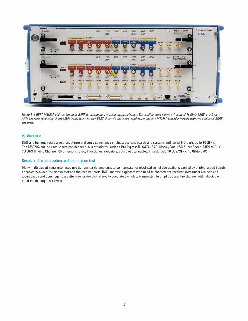
Figure 4. J-BERT M8020A high-performance BERT for accelerated receiver characterization. The configuration shows a 4 channel 16 Gb/s BERT in a 5-slot AXIe chasssis consisting of one M8041A module with two BERT channels and clock synthesizer and one M8051A extender module with two additional BERT channels.
6
User interface and measurements
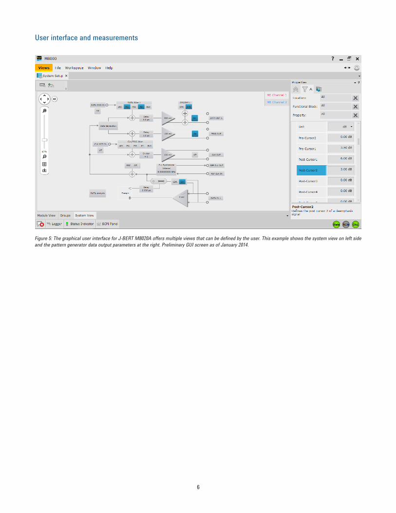
Figure 5: The graphical user interface for J-BERT M8020A offers multiple views that can be defined by the user. This example shows the system view on left side and the pattern generator data output parameters at the right. Preliminary GUI screen as of January 2014.
7
Accuracy and performance
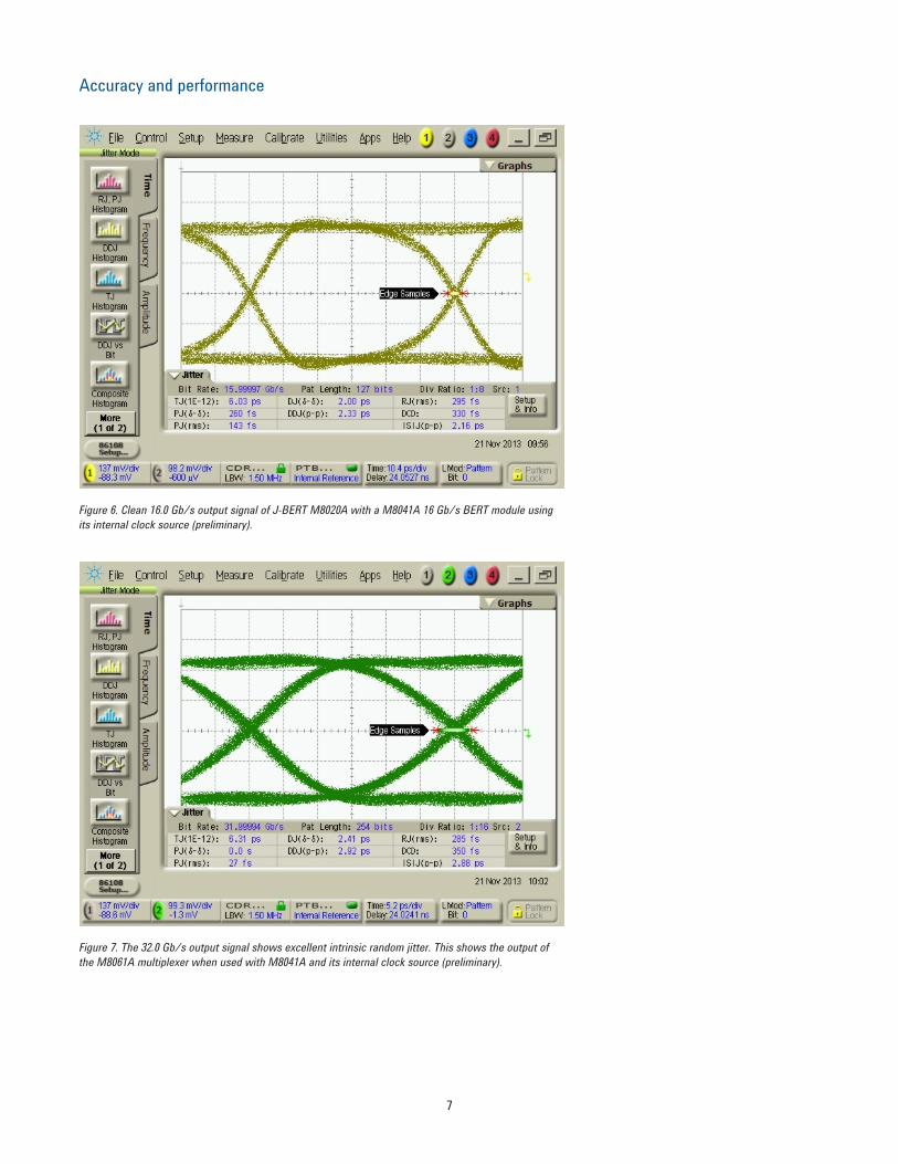
Figure 6. Clean 16.0 Gb/s output signal of J-BERT M8020A with a M8041A 16 Gb/s BERT module using its internal clock source (preliminary).
Figure 7. The 32.0 Gb/s output signal shows excellent intrinsic random jitter. This shows the output of the M8061A multiplexer when used with M8041A and its internal clock source (preliminary).
8
Specifications for M8041A and M8051A J-BERT high-performance BERT modules
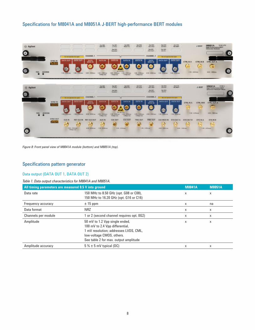
Figure 8: Front panel view of M8041A module (bottom) and M8051A (top).
Specifications pattern generator
Data output (DATA OUT 1, DATA OUT 2)Table 1. Data output characteristics for M8041A and M8051A.All timing parameters are measured 0.5 V into ground M8041A M8051AData rate 150 MHz to 8.50 GHz (opt. G08 or C08),
150 MHz to 16.20 GHz (opt. G16 or C16)x x
Frequency accuracy ± 15 ppm x naData format NRZ x xChannels per module 1 or 2 (second channel requires opt. 0G2) x xAmplitude 50 mV to 1.2 Vpp single ended,
100 mV to 2.4 Vpp differential,1 mV resolution; addresses LVDS, CML, low-voltage CMOS, others.See table 2 for max. output amplitude
x x
Amplitude accuracy 5 % ± 5 mV typical (DC) x x
9
Table 1 (CONT’D). Data output characteristics for M8041A and M8051A.M8041A M8051A
Output voltage window -1 V to +3.0 V x xExternal termination voltage -1 V to +3.0 V. For offset > 1.3 V the termination voltage should
be ± 0.5 V of offsetx x
Transition time 15 to 20 ps typical (20%-80%) x xCrossing point Adjustable from 30% to 70% x xTotal intrinsic jitter 1 8 ps p-p typical x xRandom intrinsic jitter 2 300 fs rms typical x xData delay range 0 to 10 ns x xData delay resolution 100 fs x xElectrical idle transition time Output transitions from full swing signal to 0 V amplitude and
vice versa at constant offset within 4 ns typical. Electrical idle can be controlled from sequencer or external input.
x x
Termination 50 Ω into GND or external termination voltage.Do not operate into open. Unused outputs must be terminated into termination voltage.
x x
Termination modes Balanced/unbalancedDC/AC coupling
x x
Connectors 3.5 mm, female x x
1. At 16 Gb/s PRBS 2 15-1, BER 10 -12, with internal clock.2. At 16 Gb/s and clock pattern.
Table 2. Data output amplitude maximum (single ended) in presence of DMI, CMI, offset voltage.Offset < 1.9 V Offset > 1.9 V CMI DMI1.2 Vpp 0.9 Vpp disabled disabled0.9 Vpp 0.675 Vpp disabled enabled0.9 Vpp 0.75 Vpp enabled disabled0.675 Vpp 0.562 Vpp enabled enabled0.8 Vpp 0.666 Vpp enabled enabled 1
1. For DMI < 12.5 % of amplitude.
10
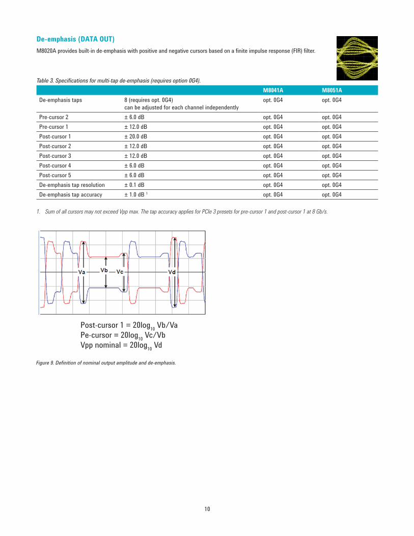
De-emphasis (DATA OUT) M8020A provides built-in de-emphasis with positive and negative cursors based on a finite impulse response (FIR) filter.
Table 3. Specifications for multi-tap de-emphasis (requires option 0G4).M8041A M8051A
De-emphasis taps 8 (requires opt. 0G4)can be adjusted for each channel independently
opt. 0G4 opt. 0G4
Pre-cursor 2 ± 6.0 dB opt. 0G4 opt. 0G4Pre-cursor 1 ± 12.0 dB opt. 0G4 opt. 0G4Post-cursor 1 ± 20.0 dB opt. 0G4 opt. 0G4Post-cursor 2 ± 12.0 dB opt. 0G4 opt. 0G4Post-cursor 3 ± 12.0 dB opt. 0G4 opt. 0G4Post-cursor 4 ± 6.0 dB opt. 0G4 opt. 0G4Post-cursor 5 ± 6.0 dB opt. 0G4 opt. 0G4De-emphasis tap resolution ± 0.1 dB opt. 0G4 opt. 0G4De-emphasis tap accuracy ± 1.0 dB 1 opt. 0G4 opt. 0G4
1. Sum of all cursors may not exceed Vpp max. The tap accuracy applies for PCIe 3 presets for pre-cursor 1 and post-cursor 1 at 8 Gb/s.
Post-cursor 1 = 20log10 Vb/VaPe-cursor = 20log10 Vc/VbVpp nominal = 20log10 Vd
Figure 9. Definition of nominal output amplitude and de-emphasis.
11
Clock output (CLK OUT) Table 4. Clock output specifications (M8041A only).
M8041A M8051AFrequency range 150 MHz to 8.50 GHz (opt. G08 or C08),
150 MHz to 16.20 GHz (opt. G16 or C16) x no clk
Amplitude 0.1 to 1 V, 5 mV steps, single ended xOutput voltage window -1 V to +3 V 1 xExternal termination voltage -1 V to +3.0 V xTransition times 20 ps typical (20%-80%) xDuty cycle 50%, accuracy ± 10% xClock divider 1, 2, 4, 8, 10, 16, 20, 24, 30, 32, 40, 50, 64, 66, 80.
For other dividers use TRG outputx
Intrinsic random jitter 300 fs rms typical at 16.2 GHz xSSB phase noise TBD xTermination 50 Ω into GND or external termination voltage. Do not operate into open.
Unused outputs must be terminated into termination voltage.x
Connectors 3.5 mm, female x
1. If Vterm is other than 0 V the following applies: high level voltage range = Vterm -1 V to 3 V and low level voltage range = -1 V to Vterm +1 V.
Reference clock input (REF CLK IN)This input on the M8041A module allows locking the system clock to an external reference clock of 10 or 100 MHz instead of the internal oscillator. Output clocks of 8 to 16 GHz.
Table 5. Reference clock input specifications (M8041A only).M8041A M8051A
Input amplitude 0.2 to 1.4 Vpp x noInput frequency 10 MHz to 16.2 GHz xInterface Single ended. 50 Ω nominal xConnector SMA, female x
Table 6. Predefined settings for reference clock multiplier (M8041A with option 0G6 only).Ref clock input Standard Target data rate Multiplier PLL loop BW M8041A 100 MHz PCIe 4 16 Gb/s 160 TBD 0G6100 MHz PCIe 3 8 Gb/s 80 5 MHz 0G6 100 MHz PCIe 2 5 Gb/s 50 5 MHz 0G6 100 MHz PCIe 1 2.5 Gb/s 25 5 MHz 0G6 26 MHz to 52 MHz SD UHS-II 390 Mb/s to 780 Mb/s 15 2 MHz 0G626 MHz to 52 MHz SD UHS-II 780 MHz to 1.56 Gb/s 30 2 MHz 0G6 52 MHz to 104 MHz SD UHS-II Gen 2 1.56 Gb/s to 3.12 Gb/s 30 TBD 0G652 MHz to 104 MHz SD UHS-II Gen 2 3.12 Gb/s to 6.24 Gb/s 30 TBD 0G619.2 MHz MIPI M-PHY 1.248/ 1.4592/ 2.496/
2.9184/ 4.992/ 5.8368 Gb/s TBD 2 MHz 0G6
26 MHz MIPI M-PHY 1.248/ 1.456/ 2.496/ 2.912/ 4.992/ 5.824 Gb/s
TBD 2 MHz 0G6
38.4 MHz MIPI M-PHY 1.248/ 1.4592/ 2.496/ 2.9184/ 4.992/ 5.8368 Gb/s
TBD 2 MHz 0G6
52 MHz MIPI M-PHY 1.248/ 1.456/ 2.496/ 2.912/ 4.992/ 5.824 Gb/s
TBD 2 MHz 0G6
12
Supplementary inputs and outputs of M8041A and M8051ATrigger output (TRG OUT)
Table 7. Trigger output specifications (M8041A only).M8041A M8051A
Amplitude 0.1 to 1 Vpp single ended; 0.2 to 2 Vpp differential
x no trg
Output voltage window -1 to 3 V 1 xExternal termination voltage -1 to 3 V xInterface Differential, 50 Ω xConnector 3.5 mm, female x
1. If Vterm is other than 0 V the following applies: high level voltage range = Vterm -1 V to 3 V and low level voltage range = -1 V to Vterm +1 V.
Reference clock output (REF CLK OUT)Outputs a 10 MHz clock, 1 Vpp single ended into 50 Ω. M8041A only.Connector: SMA, female. Clock input (CLK IN)For future use. For M8041A only. Control input A and B (CTRL IN A, CTRL IN B)Functionality of each input can be selected as: sequence trigger, error add input.
Table 8. Control input specifications (M8041A and M8051A).M8041A M8051A
Input voltage -1 V to +3 V x xTermination voltage -1 V to +3 V x xThreshold voltage -1 V to +3 V x xConnector SMA, female x x
Control output A (CTRL OUT A)Outputs a pulse in case of an error.
Table 9. Control output specifications (M8041A and M8051A).M8041A M8051A
Amplitude 1 0.1 to 2 V x xOutput voltage 1 -0.5 to 1.75 V x xConnector SMA, female x x
1. When terminated with 50 Ω into GND. Doubles into open.
Synchonization input and output (SYNC IN, SYNC OUT)The Sync output on M8041A: clock output to synchronize multiple modules to a common clock.The Sync input is a clock input on M8051A module to synchronize additional modules to a common clock.A sync cable is delivered with each M8051A module by default.
13
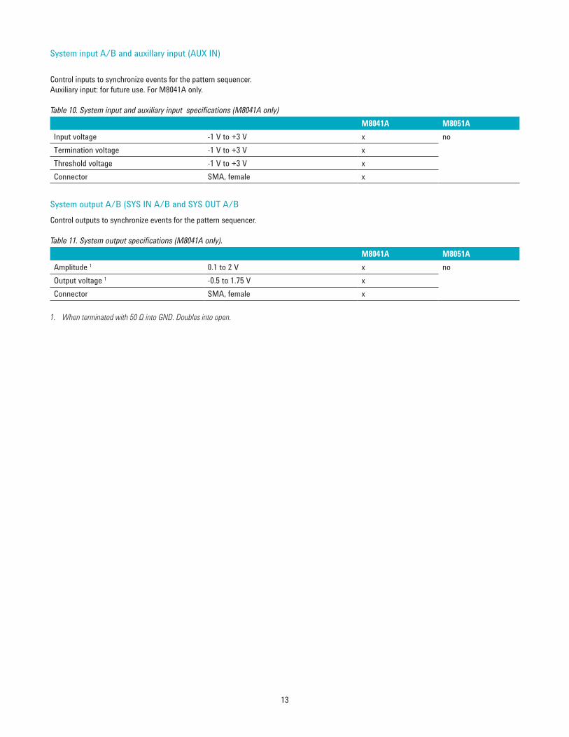
System input A/B and auxillary input (AUX IN)
Control inputs to synchronize events for the pattern sequencer.Auxiliary input: for future use. For M8041A only.
Table 10. System input and auxiliary input specifications (M8041A only)M8041A M8051A
Input voltage -1 V to +3 V x noTermination voltage -1 V to +3 V xThreshold voltage -1 V to +3 V xConnector SMA, female x
System output A/B (SYS IN A/B and SYS OUT A/BControl outputs to synchronize events for the pattern sequencer.
Table 11. System output specifications (M8041A only).M8041A M8051A
Amplitude 1 0.1 to 2 V x noOutput voltage 1 -0.5 to 1.75 V xConnector SMA, female x
1. When terminated with 50 Ω into GND. Doubles into open.
14
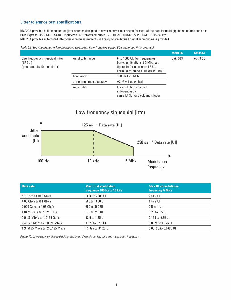
Jitter tolerance test specifications
M8020A provides built-in calibrated jitter sources designed to cover receiver test needs for most of the popular multi-gigabit standards such as: PCIe Express, USB, MIPI, SATA, DisplayPort, CPU frontside buses, CEI, 10GbE, 100GbE, SFP+, QSFP, CFP2/4, etc. M8020A provides automated jitter tolerance measurements. A library of pre-defined compliance curves is provided.
Table 12. Specifications for low frequency sinusoidal jitter (requires option 0G3 advanced jitter sources).M8041A M8051A
Low frequency sinusoidal jitter (LF SJ )(generated by IQ modulator)
Amplitude range 0 to 1000 UI. For frequencies between 10 kHz and 5 MHz see figure 10 for maximum LF SJ. Formula for fmod > 10 kHz is TBD.
opt. 0G3 opt. 0G3
Frequency 100 Hz to 5 MHzJitter amplitude accuracy ±2 % ± 1 ps typicalAdjustable For each data channel
independently, same LF SJ for clock and trigger
Data rate Max UI at modulationfrequency 100 Hz to 10 kHz
Max UI at modulationfrequency 5 MHz
8.1 Gb/s to 16.2 Gb/s 1000 to 2000 UI 2 to 4 UI4.05 Gb/s to 8.1 Gb/s 500 to 1000 UI 1 to 2 UI2.025 Gb/s to 4.05 Gb/s 250 to 500 UI 0.5 to 1 UI1.0125 Gb/s to 2.025 Gb/s 125 to 250 UI 0.25 to 0.5 UI506.25 Mb/s to 1.0125 Gb/s 62.5 to 1.25 UI 0.125 to 0.25 UI253.125 Mb/s to 506.25 Mb/s 31.25 to 62.5 UI 0.0625 to 0.125 UI126.5625 Mb/s to 253.125 Mb/s 15.625 to 31.25 UI 0.03125 to 0.0625 UI
Figure 10. Low frequency sinusoidal jitter maximum depends on data rate and modulation frequency.
Low frequency sinusoidal jitter
Jitteramplitude
(UI)
Modulationfrequency
125 ns * Data rate [UI]
250 ps * Data rate [UI]
100 Hz 10 kHz 5 MHz
15
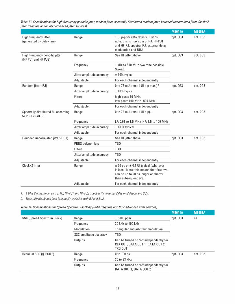
Table 13. Specifications for high frequency periodic jitter, random jitter, spectrally distributed random jitter, bounded uncorrelated jitter, Clock/2 jitter (requires option 0G3 advanced jitter sources).
M8041A M8051AHigh frequency jitter (generated by delay line)
Range 1 UI p-p for data rates > 1 Gb/snote: this is max sum of RJ, HF-PJ1 and HF-PJ, spectral RJ, external delay modulation and BUJ.
opt. 0G3 opt. 0G3
High frequency periodic jitter (HF PJ1 and HF PJ2)
Range See HF jitter above 1 opt. 0G3 opt. 0G3
Frequency 1 kHz to 500 MHz two tone possible. Sweep.
Jitter amplitude accuracy ± 10% typicalAdjustable For each channel independently
Random jitter (RJ) Range 0 to 72 mUI rms (1 UI p-p max.) 1 opt. 0G3 opt. 0G3Jitter amplitude accuracy ± 10% typicalFilters high-pass: 10 MHz,
low-pass: 100 MHz, 500 MHzAdjustable For each channel independently
Spectrally distributed RJ according to PCIe 2 (sRJ) 2
Range 0 to 72 mUI rms (1 UI p-p), 1 opt. 0G3 opt. 0G3
Frequency LF: 0.01 to 1.5 MHz, HF: 1.5 to 100 MHzJitter amplitude accuracy ± 10 % typicalAdjustable For each channel independently
Bounded uncorrelated jitter (BUJ) Range See HF jitter above1 opt. 0G3 opt. 0G3PRBS polynomials TBDFilters TBDJitter amplitude accuracy TBDAdjustable For each channel independently
Clock/2 jitter Range ± 20 ps or ± 0.1 UI typical (whatever is less). Note: this means that first eye can be up to 20 ps longer or shorter than subsequent eye.
Adjustable For each channel independently
1. 1 UI is the maximum sum of RJ, HF-PJ1 and HF-PJ2, spectral RJ, external delay modulation and BUJ.2. Spectrally distributed jitter is mutually exclusive with RJ and BUJ.
Table 14. Specifications for Spread Spectrum Clocking (SSC) (requires opt. 0G3: advanced jitter sources).M8041A M8051A
SSC (Spread Spectrum Clock) Range ± 5000 ppm opt. 0G3 naFrequency 30 kHz to 100 kHzModulation Triangular and arbitrary modulationSSC amplitude accuracy TBDOutputs Can be turned on/off independently for
CLK OUT, DATA OUT 1, DATA OUT 2, TRG OUT
Residual SSC (@ PCIe2) Range 0 to 100 ps opt. 0G3 opt. 0G3Frequency 30 to 33 kHzOutputs Can be turned on/off independently for
DATA OUT 1, DATA OUT 2
16
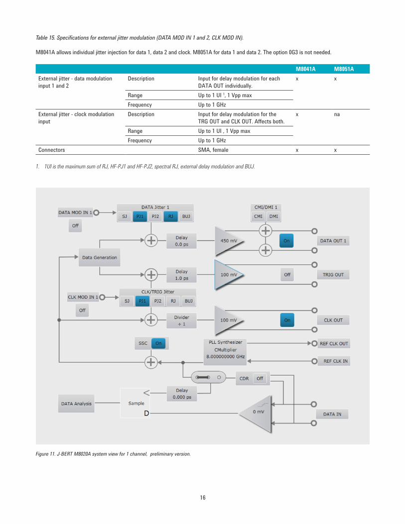
Table 15. Specifications for external jitter modulation (DATA MOD IN 1 and 2, CLK MOD IN).
M8041A allows individual jitter injection for data 1, data 2 and clock. M8051A for data 1 and data 2. The option 0G3 is not needed.
M8041A M8051AExternal jitter - data modulation input 1 and 2
Description Input for delay modulation for each DATA OUT individually.
x x
Range Up to 1 UI 1, 1 Vpp maxFrequency Up to 1 GHz
External jitter - clock modulation input
Description Input for delay modulation for the TRG OUT and CLK OUT. Affects both.
x na
Range Up to 1 UI , 1 Vpp maxFrequency Up to 1 GHz
Connectors SMA, female x x
1. 1UI is the maximum sum of RJ, HF-PJ1 and HF-PJ2, spectral RJ, external delay modulation and BUJ.
Figure 11. J-BERT M8020A system view for 1 channel, preliminary version.
17
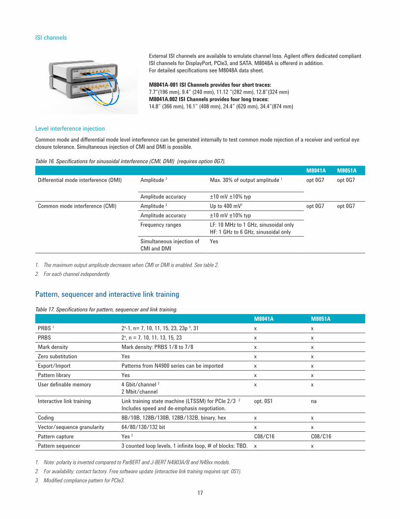
ISI channels
External ISI channels are available to emulate channel loss. Agilent offers dedicated compliant ISI channels for DisplayPort, PCIe3, and SATA. M8048A is offererd in addition. For detailed specifications see M8048A data sheet.
M8041A-001 ISI Channels provides four short traces: 7.7”(196 mm), 9.4” (240 mm), 11.12 “(282 mm), 12.8”(324 mm)M8041A.002 ISI Channels provides four long traces: 14.8” (366 mm), 16.1” (408 mm), 24.4” (620 mm), 34.4”(874 mm)
Level interference injectionCommon mode and differential mode level interference can be generated internally to test common mode rejection of a receiver and vertical eye closure tolerance. Simultaneous injection of CMI and DMI is possible.
Table 16. Specifications for sinusoidal interference (CMI, DMI) (requires option 0G7).M8041A M8051A
Differential mode interference (DMI) Amplitude 2 Max. 30% of output amplitude 1 opt 0G7 opt 0G7
Amplitude accuracy ±10 mV ±10% typCommon mode interference (CMI) Amplitude 2 Up to 400 mV1 opt 0G7 opt 0G7
Amplitude accuracy ±10 mV ±10% typFrequency ranges LF: 10 MHz to 1 GHz, sinusoidal only
HF: 1 GHz to 6 GHz, sinusoidal onlySimultaneous injection of CMI and DMI
Yes
1. The maximum output amplitude decreases when CMI or DMI is enabled. See table 2.2. For each channel independently.
Pattern, sequencer and interactive link training
Table 17. Specifications for pattern, sequencer and link training.M8041A M8051A
PRBS 1 2n-1, n= 7, 10, 11, 15, 23, 23p 3, 31 x xPRBS 2n, n = 7, 10, 11, 13, 15, 23 x xMark density Mark density: PRBS 1/8 to 7/8 x xZero substitution Yes x xExport/Import Patterns from N4900 series can be imported x xPattern library Yes x xUser definable memory 4 Gbit/channel 2
2 Mbit/channelx x
Interactive link training Link training state machine (LTSSM) for PCIe 2/3 2
Includes speed and de-emphasis negotiation.opt. 0S1 na
Coding 8B/10B, 128B/130B, 128B/132B, binary, hex x xVector/sequence granularity 64/80/130/132 bit x xPattern capture Yes 2 C08/C16 C08/C16Pattern sequencer 3 counted loop levels, 1 infinite loop, # of blocks: TBD. x x
1. Note: polarity is inverted compared to ParBERT and J-BERT N4903A/B and N49xx models.2. For availability: contact factory. Free software update (interactive link training requires opt. 0S1).3. Modified compliance pattern for PCIe3.
18
Analyzer/error detector
Each analyzer channel includes a clock recovery.For the following functions a separate module option is required:• Equalizer CTLE option (option 0A3 for M8041A and M8051A)
• SER/FER analysis (option 0S2 for M8041A only, applies for all analyzers channels in the same clock group): this option provides handling of 8B/10B coded, 128B/130B coded SKPOS. Automatic handling of running disparity changes for 8B/10B coded patterns. Up to 4 filler symbols can be defined. No dead time while filtering filler symbols. Ignores changes of length of 128/130 bit coded Skip Ordered Sets for PCIe. Counters for SER/FER filler symbols.
Table 18. Specifications for analyzer / error detector (Option C08 or C16).M8041A M8051A
Data rate 150 MHz to 8.50 GHz (opt. C08), 150 MHz to 16.20 GHz (opt. C16)
x x
Channels per module 1 or 2 (opt. 0A2) x xData format NRZ, single ended and differential x xInput sensitivity 1 < 50 mV x xTiming resolution 1 mUI x xInput bandwidth TBD x xCTLE Yes opt. 0A3 opt. 0A3Clock data recovery Yes for each input channel x xAdjustable loop bandwidth Data rate /10000 to data rate/800
(maximum is 20 MHz)x x
Sampling point Manual and automatic. Finds optimum voltage threshold and delay of the sampling point.
x x
Decision threshold range TBD x xPhase margin TBD x xBER Accumulated x xSymbol/frame error rate 8B/10B, 128B/130B coded
and retimed patternsopt. 0S2 na
Filtering of filler symbols Automatic removal of filler symbols. See also description above.
opt. 0S2 na
Interface Differential: 100 Ω, single ended: 50 Ω, DC coupled x xData input connectors 3.5 mm, female x x
1. Measured with PRBS 2 31-1 at 16 Gb/s single ended, target BER 10 -12.
Table 18. Specifications for analyzer / error detector (Option C08 or C16).M8041A M8051A
BERT Scan with RJ, DJ separation Yes x xAccumulated BER Yes x xJitter tolerance Yes x xEye contour Yes 1 x xQuick eye diagram Yes 1 x xOutput level and Q factor Yes 1 x x
1. For availability: contact factory. Free software update.
19
User interface and remote control
The M8070A system software for the M8000 Series of BER Test Solutions is required to control M8041A, M8051A and M8061A.
Table 18. User interface and remote control interface.System software M8070ASoftware licensing Offline version does not require a license. For controlling the hardware you can choose
between a transportable, perpetual license (M8070A-0TP) and a network, perpetual license (M8070A-0NP) . The network license is only recommended when using multiple M8020A setups within one company. When ordering M8020A-BU1 the M8070A-0TP license will be pre-installed on the embedded controller.
Controller requirements Embedded PC: Choose M8020A-BU1 for a pre-installed embedded controller M9536A including pre-installation of M8070A software and module licenses. Otherwise: M9536A 1-slot AXIe embedded controller, choose options for Windows 7 or 8, 16 GB RAM, USBExternal PC: USB connection recommended between external PC and AXIe chassis. Minimum of 8 GB RAM recommended. For PCIe connectivity please refer to list of tested PCs for AXIe Technical Note, pub no. 5990-7632EN
Operating system Microsoft Windows 7 (64 bit) SP1, Windows 8 (64 bit)Controller connectivity with AXIe chassis USB 2.0 (mini) recommended,
PCIe 2.0/8x (only for highest data throughput and desktop PC)Programming language SCPI. Not compatible with N4900 series and ParBERT 81250ARemote control interface Desktop or Laptop PC: LAN
M9536A: LANSave/Recall YesSoftware pre-requisites Microsoft Win 7 SP1 or 8, Agilent IO library rev. 16.3Software download See www.agilent.com/find/m8020a for latest version
20
General characteristics and physical dimensions
Table 19. General characteristics for M8041A and M8051A modules.M8041A M8051A
Operating temperature 5 °C to 40 °C (-23 °F to + 104 °F)Storage temperature -40 ºC to +70 ºC (modules) (-65 °F to + 158 °F)Operating humidity 15% to 95% relative humidity at 40ºC (non-condensing)Storage humidity 24% to 90% relative humidity at 65ºC (non-condensing)Power requirements 350 W 250 WPhysical dimensions for modules(W x H x D)
3- slot AXIe module: 351 x 92 x 315 mm (13.8 x 3.6 x 12.4 inch)
2-slot AXIe module:351 x 61 x 315 mm (13.8 x 2.4 x 12.4 inch)
Physical dimensions for M8020A-BU1/-BU2(W x H x D)
Installed in 5-slot AXIe chassis:463 x 194 x 446 mm
(18.2 x 7.6 x 17.6 inch)Weight net M8041A module: 6.6 kg (14.6 lb)
With M8020A-BU1: 24 kg (43.9 lb)With M8020A-BU2: 19.9 kg (53 lb)
M8051A module: 5.0 kg (11.0 lb)In bundle with M8041A and in a 5-slot chassis: 24.9 kg (54.9 lb)
Weight shipping With M8020A-BU1: 37 kg (82 lb)With M8020A-BU2: 32.5 kg (71.7 lb)
N/A
Recommended recalibration period 1 yearWarranty period 3 years return to AgilentWarm-up time 30 minutesCooling requirements Slot airflow direction is from right to left. When operating the M8041A/51A choose a
location that provides at least 80 mm of clearance at rear, and at least 30 mm of clearance at each side. See also start-up guide for M9502A chassis.
EMC IEC 61326-1Safety IEC 61010-1Quality management ISO 9001, 14001
21
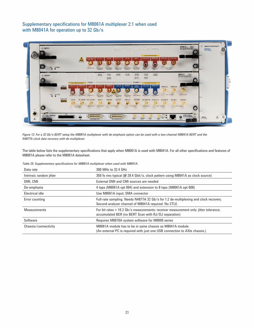
Supplementary specifications for M8061A multiplexer 2:1 when used with M8041A for operation up to 32 Gb/s
Figure 12: For a 32 Gb/s BERT setup the M8061A multiplexer with de-emphasis option can be used with a two-channel M8041A BERT and the N4877A clock data recovery with de-multiplexer.
The table below lists the supplementary specifications that apply when M8061A is used with M8041A. For all other specifications and features of M8061A please refer to the M8061A datasheet.
Table 20. Supplementary specifications for M8061A multiplexer when used with M8041A.
Data rate 300 MHz to 32.4 GHz Intrinsic random jitter 350 fs rms typical (@ 28.4 Gbit/s, clock pattern using M8041A as clock source) DMI, CMI External DMI and CMI sources are neededDe-emphasis 4 taps (M8061A opt 004) and extension to 8 taps (M8061A opt 008)Electrical idle Use M8061A input; SMA connectorError counting Full-rate sampling. Needs N4877A 32 Gb/s for 1:2 de-multiplexing and clock recovery.
Second analyzer channel of M8041A required. No CTLE. Measurements For bit rates > 16.2 Gb/s measurements: receiver measurement only: jitter tolerance,
accumulated BER (no BERT Scan with RJ/DJ separation) Software Requires M8070A system software for M8000 seriesChassis/connectivity M8061A module has to be in same chassis as M8041A module.
(An external PC is required with just one USB connection to AXIe chassis.)
22
Specification assumptionsThe specifications in this document describe the instruments warranted performance. Preliminary values are written in italic. Non-warranted values are described as typical. All specifications are valid in the specified operating temperature range after the warm-up time and after auto-adjustment. If not otherwise stated all outputs need to be terminated with 50 Ω to GND. All M8041A and M8051A specifications if not otherwise stated are valid using the recommended cable pair M8041A-801 (2.92 mm, 0.85 m, matched pair).
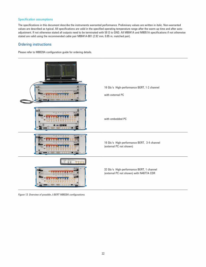
Ordering instructions
Please refer to M8020A configuration guide for ordering details.
16 Gb/s High-performance BERT, 1-2 channel
with external PC
with embedded PC
16 Gb/s High-performance BERT, 3-4 channel(external PC not shown)
32 Gb/s High-performance BERT, 1 channel(external PC not shown) with N4877A CDR
Figure 13. Overview of possible J-BERT M8020A configurations.
23
Default accessories included with shipment:M8041A module: eight 50 Ω terminations, commercial calibration report (“UK6”), certificate of calibration, ESD protection kit.M8051A module: four 50 Ω terminations, clock synchronization cable, commercial calibration report (“UK6”), certificate of calibrationM8020A-BU1: M9505A AXIe chassis with embedded controller, USB cable, getting started guide, AXIe filler panel, power cordM8020A-BU2: M9505A AXIe chassis, USB cable, getting started guide, AXIe filler panel, power cordM8070A: CD-ROM with M8070A system software
Recommended accessories:Matched cable pair, 2.92 mm (f) to 2.92 mm (f), 0.85 m M8041A-801(recommended for each data output of M8041A/51A. This 2.92 mm cable is compatible with 3.5 mm front panel connectors of M8041A/51A.) (two pairs are recommended for connecting M8041A with M8061A)ISI channels, four short traces M8048A-001ISI channels, four long traces M8048A-002Short matched cable pair, SMA (f) to SMA (f) for cascading M8048A ISI channels M8048A-801Four SMA cables, unmatched 15442ARack-mount kit for AXIe 5-slot chassis M9505A TBD
Test automation software with support of M8020ATest automation software for PCIe receiver test N5990A-101Test automation software for USB receiver test N5990A-102Test automation software for SATA receiver test N5990A-103PCIe link training suite N5990A-301
Warranty, calibration and productivity services:Extended 5 year warranty Return-to-Agilent R1280 (R-51B-001-5Z)Calibration services (3 and 5 years) R1282Productivity assistance R1380-M8000
Related Agilent literature
Data sheets and configuration guides:M8048A ISI Channels Data Sheet 5991-3548ENM8061A Multiplexer with de-emphasis Data Sheet 5991-2506ENJ-BERT N4903B high-performance BERT Data Sheet 5990-3217ENN4877A and N1075A CDR/Demux Data Sheet 5990-9949ENM9505A AXIe Chassis 5-slot Data Sheet 5990-6584ENM8020A Configuration Guide 5991-4032EN
Application notes:Master your MIPI M-PHY receiver test using J-BERT M8020A Application Brief 5991-3959ENHow to pass receiver test according PCI Express CEM specification Application Note 5990-7659ENAccurate calibration of PCIe 3.0 receiver stress signals Application Note 5990-6599ENHow to test a MIPI M-PHY high-speed receiver Application Note 5991-2848EN
myAgilent
myAgilent
www.agilent.com/find/myagilentA personalized view into the information most relevant to you.
Three-Year Warranty
www.agilent.com/find/ThreeYearWarrantyBeyond product specification, changing the ownership experience.Agilent is the only test and measurement company that offers three-year warranty on all instruments, worldwide.
Agilent Assurance Plans
www.agilent.com/find/AssurancePlansFive years of protection and no budgetary surprises to ensure your instruments are operating to specifications and you can continually rely on accurate measurements.
www.agilent.com/quality
Agilent Electronic Measurement GroupDEKRA Certified ISO 9001:2008 Quality Management System
Agilent Channel Partners
www.agilent.com/find/channelpartnersGet the best of both worlds: Agilent’s measurement expertise and product breadth, combined with channel partner convenience.
Agilent Solution Partners
www.agilent.com/find/solutionpartnersGet the best of both worlds: Agilent’s measurement expertise and product breadth, combined with solution partner convenience.
www.agilent.comwww.agilent.com/find/m8020a
For more information on Agilent Technologies’ products, applications or services, please contact your local Agilent office. The complete list is available at:www.agilent.com/find/contactus
AmericasCanada (877) 894 4414 Brazil (11) 4197 3600Mexico 01800 5064 800 United States (800) 829 4444Asia PacificAustralia 1 800 629 485China 800 810 0189Hong Kong 800 938 693India 1 800 112 929Japan 0120 (421) 345Korea 080 769 0800Malaysia 1 800 888 848Singapore 1 800 375 8100Taiwan 0800 047 866Other AP Countries (65) 375 8100Europe & Middle EastBelgium 32 (0) 2 404 93 40 Denmark 45 45 80 12 15Finland 358 (0) 10 855 2100France 0825 010 700* *0.125 €/minuteGermany 49 (0) 7031 464 6333 Ireland 1890 924 204Israel 972-3-9288-504/544Italy 39 02 92 60 8484Netherlands 31 (0) 20 547 2111Spain 34 (91) 631 3300Sweden 0200-88 22 55United Kingdom 44 (0) 118 927 6201
For other unlisted countries:www.agilent.com/find/contactus(BP-01-15-14)
Product specifications and descriptions in this document subject to change without notice.
© Agilent Technologies, Inc. 2014Published in USA, February 26, 20145991-3647ENPCIe and PCI Express are registered trademarks of the PCI-SIG.