algorithms for electronic design automationmustafa.ozdal/cs612/slides/lecture4.pdf · vlsi physical...
TRANSCRIPT

1
CS612 Algorithms for Electronic Design Automation
CS 612 – Lecture 4
Floorplanning
Mustafa Ozdal
Computer Engineering Department, Bilkent University
Mustafa Ozdal

VLSI Physical Design: From Graph Partitioning to Timing Closure Chapter 2: Netlist and System Partitioning
© K
LM
H
Lie
nig
2
Chapter 2 – Netlist and System Partitioning
Original Authors:
Andrew B. Kahng, Jens Lienig, Igor L. Markov, Jin Hu
VLSI Physical Design: From Graph Partitioning to Timing Closure
SOME SLIDES ARE FROM THE BOOK:
MODIFICATIONS WERE MADE ON THE ORIGINAL SLIDES

VLSI Physical Design: From Graph Partitioning to Timing Closure Chapter 2: Netlist and System Partitioning
© K
LM
H
Lie
nig
3
3.1 Introduction
ENTITY test is
port a: in bit;
end ENTITY test;
DRC
LVS
ERC
Circuit Design
Functional Design
and Logic Design
Physical Design
Physical Verification
and Signoff
Fabrication
System Specification
Architectural Design
Chip
Packaging and Testing
Chip Planning
Placement
Signal Routing
Partitioning
Timing Closure
Clock Tree Synthesis

VLSI Physical Design: From Graph Partitioning to Timing Closure Chapter 3: Chip Planning
© K
LM
H
Lie
nig4
3.1 Introduction
GND VDD
Module e
I/O Pads
Block Pins
Block a
Block
b
Block d
Block e
Floorplan
Module d
Module c
Module b
Module a
Chip
Planning
Block c
Supply Network
© 2
011 S
prin
ger
Verla
g

5CS 612 – Lecture 4 Mustafa Ozdal
Computer Engineering Department, Bilkent University
Floorplanning
Circuit modules obtained through partitioning
either automatic or manual partitioning
Floorplanning: Assign shapes and locations for all
circuit modules.

VLSI Physical Design: From Graph Partitioning to Timing Closure Chapter 3: Chip Planning
© K
LM
H
Lie
nig6
3.1 Introduction
Example
Given: Three blocks with the following potential widths and heights
Block A: w = 1, h = 4 or w = 4, h = 1 or w = 2, h = 2
Block B: w = 1, h = 2 or w = 2, h = 1
Block C: w = 1, h = 3 or w = 3, h = 1
Task: Floorplan with minimum total area enclosed
A
A
A
B
BC
C

VLSI Physical Design: From Graph Partitioning to Timing Closure Chapter 3: Chip Planning
© K
LM
H
Lie
nig7
3.1 Introduction
Example
Given: Three blocks with the following potential widths and heights
Block A: w = 1, h = 4 or w = 4, h = 1 or w = 2, h = 2
Block B: w = 1, h = 2 or w = 2, h = 1
Block C: w = 1, h = 3 or w = 3, h = 1
Task: Floorplan with minimum total area enclosed

VLSI Physical Design: From Graph Partitioning to Timing Closure Chapter 3: Chip Planning
© K
LM
H
Lie
nig8
3.1 Introduction
Solution:
Aspect ratios
Block A with w = 2, h = 2; Block B with w = 2, h = 1; Block C with w = 1, h = 3
This floorplan has a global bounding box with minimum possible area (9 square units).
Example
Given: Three blocks with the following potential widths and heights
Block A: w = 1, h = 4 or w = 4, h = 1 or w = 2, h = 2
Block B: w = 1, h = 2 or w = 2, h = 1
Block C: w = 1, h = 3 or w = 3, h = 1
Task: Floorplan with minimum total area enclosed

9CS 612 – Lecture 4 Mustafa Ozdal
Computer Engineering Department, Bilkent University
Optimization Objectives
Minimize the area of the global bounding box
Aspect ratio constraints due to packaging and
manufacturing limitations (e.g. a square chip)
Minimize the total wirelength between blocks
Long connections increase signal delays (lower performance)
More wirelength can degrade routability
More wirelength increases power (due to wire capacitances)

10CS 612 – Lecture 4
Combination of area(F) and total wirelength L(F) of
floorplan F
Minimize α ∙ area(F) + (1 – α) ∙ L(F)
where the parameter 0 ≤ α ≤ 1 gives the relative importance
between area(F) and L(F)
Mustafa Ozdal
Computer Engineering Department, Bilkent University
Objective Function: Example

11CS 612 – Lecture 4 Mustafa Ozdal
Computer Engineering Department, Bilkent University
Floorplan Representations
A floorplan can be represented based on the locations of
the blocks
Complicates generation of new overlap-free floorplans
Typical floorplanning algorithms are iterative in nature
Local search and iterative improvement heavily used
Topological representations based on relative block positions
The represented floorplan guaranteed to be overlap free
Easy to evaluate and make incremental changes

VLSI Physical Design: From Graph Partitioning to Timing Closure Chapter 3: Chip Planning
© K
LM
H
Lie
nig12
3.3 Terminology
A rectangular dissection is a division of the chip area into a set of blocks
or non-overlapping rectangles.
A slicing floorplan is a rectangular dissection
Obtained by repeatedly dividing each rectangle, starting with the entire chip area,
into two smaller rectangles
Horizontal or vertical cut line.
A slicing tree or slicing floorplan tree is a binary tree with k leaves and k – 1
internal nodes
Each leaf represents a block
Each internal node represents a horizontal or vertical cut line.

VLSI Physical Design: From Graph Partitioning to Timing Closure Chapter 3: Chip Planning
© K
LM
H
Lie
nig13
3.3 Terminology
Slicing floorplan and two possible corresponding slicing trees
b
da
e
c
f a cb
d
e f
H
V
H
H
V
H
V
H
d
c
e f
H
V
ba
© 2
011 S
prin
ger
Verla
g
VLSI Physical Design: From Graph Partitioning to Timing Closure Chapter 3: Chip Planning
© K
LM
H
Lie
nig14
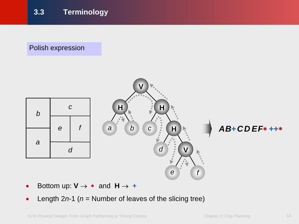
3.3 Terminology
Polish expression
b
da
e
c
f a cb
d
e f
H
V
H
H
V
B+C A D EF++
Bottom up: V and H +
Length 2n-1 (n = Number of leaves of the slicing tree)

15CS 612 – Lecture 4 Mustafa Ozdal
Computer Engineering Department, Bilkent University
slide from M. D. F. Wong, “On Simulated Annealing in EDA”, ISPD 2012

VLSI Physical Design: From Graph Partitioning to Timing Closure Chapter 3: Chip Planning
© K
LM
H
Lie
nig16
3.3 Terminology
Non-slicing floorplans (wheels)
b
d
a
eca
bc
d
e
© 2
011 S
prin
ger
Verla
g

VLSI Physical Design: From Graph Partitioning to Timing Closure Chapter 3: Chip Planning
© K
LM
H
Lie
nig17
3.3 Terminology
Floorplan tree: Tree that represents a hierarchical floorplan
a
b
c
d
e
f
g
h
i
H
H
HH
V
W h i
c d e f ga b
© 2
011 S
prin
ger
Verla
g
HHHorizontal division
(objects to the top and bottom)
HVVertical division
(objects to the left and right)
HWWheel (4 objects cycled
around a center object)
18CS 612 – Lecture 4 Mustafa Ozdal
Computer Engineering Department, Bilkent University
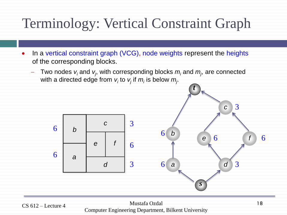
Terminology: Vertical Constraint Graph
In a vertical constraint graph (VCG), node weights represent the heights
of the corresponding blocks.
Two nodes vi and vj, with corresponding blocks mi and mj, are connected
with a directed edge from vi to vj if mi is below mj.
b
da
e
c
f
a
b
d
c
e f
s
t
6
63
6
3 6
6
3
66
3

19CS 612 – Lecture 4 Mustafa Ozdal
Computer Engineering Department, Bilkent University
Terminology: Horizontal Constraint Graph
In a horizontal constraint graph (HCG), node weights represent the widths
of the corresponding blocks.
Two nodes vi and vj, with corresponding blocks mi and mj, are connected
with a directed edge from vi to vj if mi is to the left of mj.
b
da
e
c
f
a
b
d
c
e fs t
3 4
2 2
3 4
3 4
2 2
20CS 612 – Lecture 4 Mustafa Ozdal
Computer Engineering Department, Bilkent University
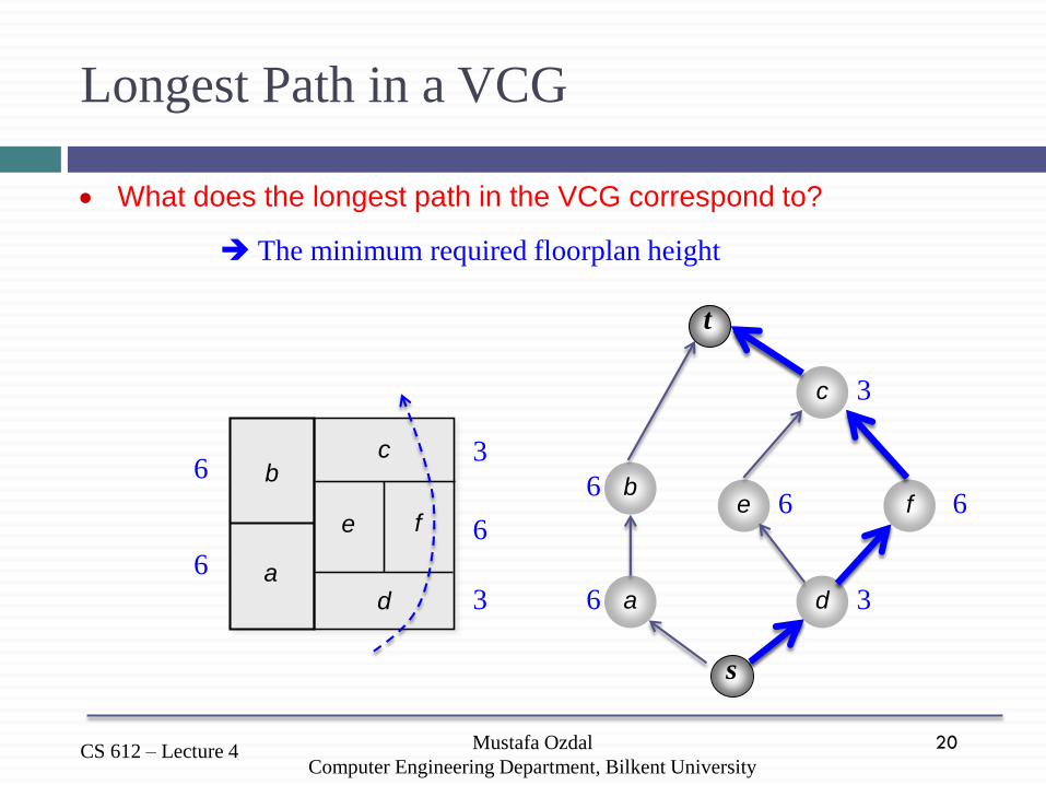
Longest Path in a VCG
What does the longest path in the VCG correspond to?
b
da
e
c
f
a
b
d
c
e f
s
t
6
63
6
3 6
6
3
66
3
The minimum required floorplan height

21CS 612 – Lecture 4 Mustafa Ozdal
Computer Engineering Department, Bilkent University
Longest Path in HCG
b
da
e
c
f
a
b
d
c
e fs t
3 4
2 2
3 4
3 4
2 2
What does the longest path in the HCG correspond to?
The minimum required floorplan width

VLSI Physical Design: From Graph Partitioning to Timing Closure Chapter 3: Chip Planning
© K
LM
H
Lie
nig22
3.3 Terminology
In a vertical constraint graph (VCG), node weights represent the heights
of the corresponding blocks.
Two nodes vi and vj, with corresponding blocks mi and mj, are connected
with a directed edge from vi to vj if mi is below mj.
In a horizontal constraint graph (HCG), node weights represent the widths
of the corresponding blocks.
Two nodes vi and vj, with corresponding blocks mi and mj, are connected
with a directed edge from vi to vj if mi is to the left of mj.
The longest path(s) in the VCG / HCG correspond(s) to the minimum vertical /
horizontal floorplan span required to pack the blocks (floorplan height / width).
A constraint-graph pair is a floorplan representation that consists of two
directed graphs – vertical constraint graph and horizontal constraint graph –
which capture the relations between block positions.

VLSI Physical Design: From Graph Partitioning to Timing Closure Chapter 3: Chip Planning
© K
LM
H
Lie
nig23
3.3 Terminology
Constraint graphs
Horizontal Constraint Graph
Vertical
Constraint
Graph
a
b
c
de
f
g
h
i
e
h
i
d
g
b
c fas
t
a
b
h
i
s
g
fc
d e
t
© 2
011 S
prin
ger
Verla
g

VLSI Physical Design: From Graph Partitioning to Timing Closure Chapter 3: Chip Planning
© K
LM
H
Lie
nig
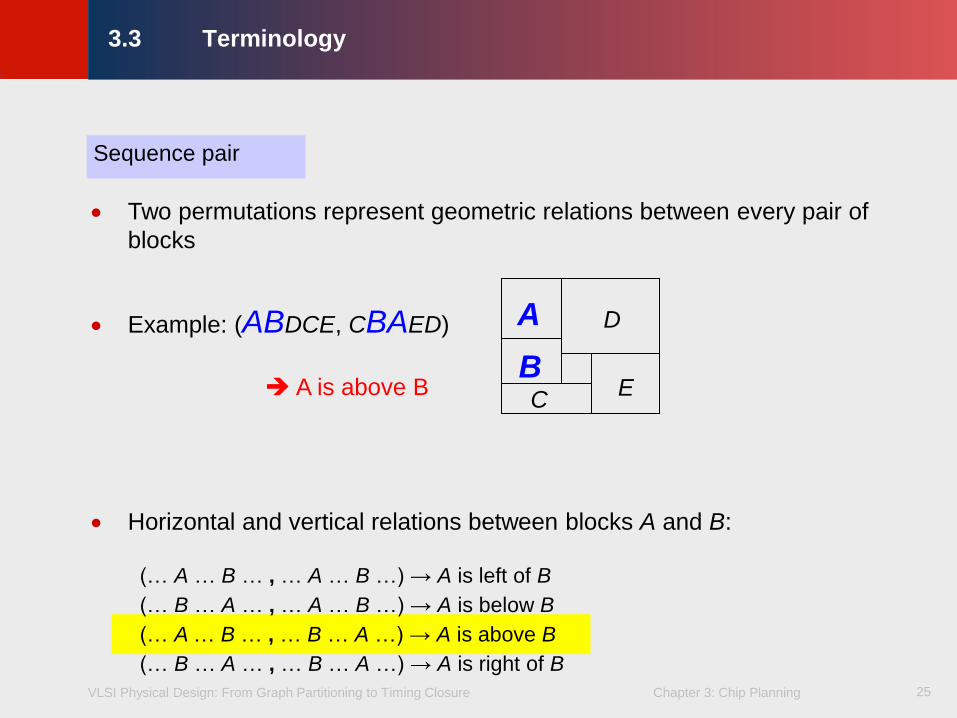
Two permutations represent geometric relations between every pair of
blocks
Example: (ABDCE, CBAED)
Horizontal and vertical relations between blocks A and B:
(… A … B … , … A … B …) → A is left of B
(… B … A … , … A … B …) → A is below B
(… A … B … , … B … A …) → A is above B
(… B … A … , … B … A …) → A is right of B
24
3.3 Terminology
Sequence pair
C
A
B
D
E
VLSI Physical Design: From Graph Partitioning to Timing Closure Chapter 3: Chip Planning
© K
LM
H
Lie
nig
Two permutations represent geometric relations between every pair of
blocks
Example: (ABDCE, CBAED)
Horizontal and vertical relations between blocks A and B:
(… A … B … , … A … B …) → A is left of B
(… B … A … , … A … B …) → A is below B
(… A … B … , … B … A …) → A is above B
(… B … A … , … B … A …) → A is right of B
25
3.3 Terminology
Sequence pair
C
A
B
D
E A is above B

VLSI Physical Design: From Graph Partitioning to Timing Closure Chapter 3: Chip Planning
© K
LM
H
Lie
nig
Two permutations represent geometric relations between every pair of
blocks
Example: (ABDCE, CBAED)
Horizontal and vertical relations between blocks A and B:
(… A … B … , … A … B …) → A is left of B
(… A … B … , … B … A …) → A is above B
(… B … A … , … A … B …) → A is below B
(… B … A … , … B … A …) → A is right of B
26
3.3 Terminology
Sequence pair
C
A
B
D
E B is left of D

27CS 612 – Lecture 4 Mustafa Ozdal
Computer Engineering Department, Bilkent University
Sequence Pair: Intuition
Sequence 1: ABDCE
Sequence 2: CBAED
C
A
B
D
E
A
BD
CE
A
CB
E
D
A
B
C
D
E

28CS 612 – Lecture 4 Mustafa Ozdal
Computer Engineering Department, Bilkent University
Sequence Pair: Intuition
Sequence 1: ABDCE
Sequence 2: CBAED
C
A
B
D
E
A
BD
CE
A
CB
E
D
A
B
C
D
E
blocks above B
blo
cks
left
of
B
blocks below Bblo
cks
right
of
B

VLSI Physical Design: From Graph Partitioning to Timing Closure Chapter 3: Chip Planning
© K
LM
H
Lie
nig2929
3.4 Floorplan Representations
3.1 Introduction to Floorplanning
3.2 Optimization Goals in Floorplanning
3.3 Terminology
3.4 Floorplan Representations
3.4.1 Floorplan to a Constraint-Graph Pair
3.4.2 Floorplan to a Sequence Pair
3.4.3 Sequence Pair to a Floorplan
3.5 Floorplanning Algorithms
3.5.1 Floorplan Sizing
3.5.2 Cluster Growth
3.5.3 Simulated Annealing
3.5.4 Integrated Floorplanning Algorithms
3.6 Pin Assignment
3.7 Power and Ground Routing
3.7.1 Design of a Power-Ground Distribution Network
3.7.2 Planar Routing
3.7.3 Mesh Routing

30CS 612 – Lecture 4 Mustafa Ozdal
Computer Engineering Department, Bilkent University
Horizontal and Vertical Constraints
A
(xA, yA)
wA
hA B
(xB, yB)
wB
hB
If xA + wA ≤ xB and ! (yA+hA ≤ yB or yB + hB ≤ yA)
A is left of B
AB
If yA + hA ≤ yB and ! (xA+wA ≤ xB or xB + wB ≤ xA)
A is below B A
B

VLSI Physical Design: From Graph Partitioning to Timing Closure Chapter 3: Chip Planning
© K
LM
H
Lie
nig31
Create nodes for every block. In addition, create a source node and a sink
one.
31
3.4.1 Floorplan to a Constraint-Graph Pair
a
c d e
s t
ba
c d e
b

VLSI Physical Design: From Graph Partitioning to Timing Closure Chapter 3: Chip Planning
© K
LM
H
Lie
nig32
Create nodes for every block. In addition, create a source node and a sink
one.
Add a directed edge (A,B) if Block A is to the left of Block B. (HCG)
32
3.4.1 Floorplan to a Constraint-Graph Pair
a
c d e
s t
ba
c d e
b

VLSI Physical Design: From Graph Partitioning to Timing Closure Chapter 3: Chip Planning
© K
LM
H
Lie
nig33
Create nodes for every block. In addition, create a source node and a sink
one.
Add a directed edge (A,B) if Block A is to the left of Block B. (HCG)
Remove the redundant edges that cannot be derived from other edges by
transitivity.
33
3.4.1 Floorplan to a Constraint-Graph Pair
a
c d e
s t
ba
c d e
b

34CS 612 – Lecture 4 Mustafa Ozdal
Computer Engineering Department, Bilkent University
Floorplan to a Sequence PairStep 1: Consider the constraints related to HCG
b
da
e
c
f
a
b
d
c
e fs tHCG
a
b
e
c
d
f
Constraints for SP 1
a
b
e
c
d
f
Constraints for SP 2
(… A… B… ,… A… B…) → A is left of B

35CS 612 – Lecture 4 Mustafa Ozdal
Computer Engineering Department, Bilkent University
Floorplan to a Sequence PairStep 2: Consider the constraints related to VCG
a
b
e
c
d
f
Constraints for SP 1
a
b
e
c
d
f
Constraints for SP 2
b
da
e
c
f
a
b
d
c
e f
s
t (… B… A… ,… A… B…)
→ A is below B

36CS 612 – Lecture 4 Mustafa Ozdal
Computer Engineering Department, Bilkent University
Floorplan to a Sequence PairStep 3: Create the sequence pairs based on the constraints
Sequence 1: bacefd Sequence 2: abdefc
b
da
e
c
f
(… A… B… ,… A… B…) → A is left of B
(… B… A… ,… A… B…) → A is below B
a
b
e
c
d
f
Constraints for SP 1
a
b
e
c
d
f
Constraints for SP 2

37CS 612 – Lecture 4 Mustafa Ozdal
Computer Engineering Department, Bilkent University
Sequence Pair to a Floorplan
Method 1 (simpler):
1. Create constraint graphs: HCG and VCG
2. Pack the blocks based on HCG and VCG (next slides)
Complexity: O(n2)
Method 2
Pack the blocks based on the sequence pair directly
Complexity: O(nlgn)

38CS 612 – Lecture 4 Mustafa Ozdal
Computer Engineering Department, Bilkent University
Constraint Graph Pair to a Floorplan
Given an HCG and a VCG, we can compute a
packing solution that satisfies all the constraints.
Basic idea:
Compute the longest path on HCG
The coordinate computed for each vertex will be the x-coordinate of the
corresponding block in the packed floorplan.
Compute the longest path on VCG
The coordinate computed for each vertex will be the y-coordinate of the
corresponding block in the packed floorplan.

39CS 612 – Lecture 4 Mustafa Ozdal
Computer Engineering Department, Bilkent University
Reminder: Longest Path Algorithm
LONGEST-PATH (G)
for each vertex u in G
coord[u] = 0
for each vertex u in G in topological order
for each edge (uv) in G do
coord[v] = max (coord[v], coord[u]+wt(u))

40CS 612 – Lecture 4 Mustafa Ozdal
Computer Engineering Department, Bilkent University
Example: Sequence Pair to a Floorplan
Compute HCG and VCG for the sequence pair:
S1 = bdcefa S2 = dbaefc
(… A… B… ,… A… B…) → A is left of B
(… B… A… ,… A… B…) → A is below B
a6
3
b6
3
c
4
3 d
4
e6
2
3f6
2

41CS 612 – Lecture 4 Mustafa Ozdal
Computer Engineering Department, Bilkent University
Example: HCG for sequence pair
d
b a
c
e fs t
S1 = bdcefa S2 = dbaefc

42CS 612 – Lecture 4 Mustafa Ozdal
Computer Engineering Department, Bilkent University
Example: VCG for Sequence Pair
S1 = bdcefa S2 = dbaefc
d
b
a
c
e f
s
t

43CS 612 – Lecture 4 Mustafa Ozdal
Computer Engineering Department, Bilkent University
Example: Longest Path in HCG
x(s) = 0
x(b) = 0
x(d) = 0
x(e) = 4
x(c) = 4
x(a) = 4
x(f) = 6
x(t) = 8 d
b a
c
e fs t
w=3
w=4
w=3
w=4
w=2 w=2

44CS 612 – Lecture 4 Mustafa Ozdal
Computer Engineering Department, Bilkent University
Example: Longest Path in VCG
d
b
a
c
e f
s
t
h=6
h=3
y(s) = 0
y(a) = 0
y(d) = 0
y(b) = 3
y(e) = 6
y(f) = 6
y(c) = 12
y(t) = 15h=6
h=6 h=6
h=3

45CS 612 – Lecture 4 Mustafa Ozdal
Computer Engineering Department, Bilkent University
Example: Packing
6 a
3
6 b
3
c
4
3 d
4
6 e
2
36 f
2
(4,0) (0,3)
(4,12) (0,0)
(4,6) (6,6)
da
b
e f
c
8
15

46CS 612 – Lecture 4 Mustafa Ozdal
Computer Engineering Department, Bilkent University
Example: Summary
The sequence pair:
S1 = bdcefa S2 = dbaefc
a6
3
b6
3
c
4
3 d
4
e6
2
3f6
2
corresponds to the packed floorplan:
da
b
e f
c
12
8
47CS 612 – Lecture 4 Mustafa Ozdal
Computer Engineering Department, Bilkent University
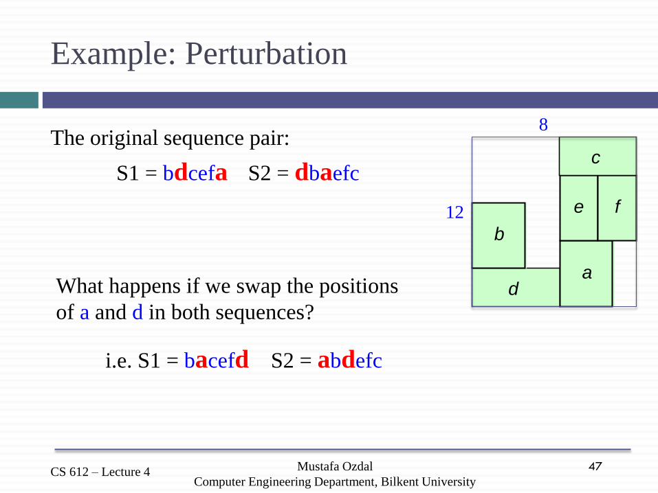
Example: Perturbation
The original sequence pair:
S1 = bdcefa S2 = dbaefc
da
b
e f
c
12
8
What happens if we swap the positions
of a and d in both sequences?
i.e. S1 = bacefd S2 = abdefc

48CS 612 – Lecture 4 Mustafa Ozdal
Computer Engineering Department, Bilkent University
Example: Longest Path in HCG after Perturbation
x(s) = 0
x(b) = 0
x(a) = 0
x(e) = 3
x(c) = 3
x(d) = 3
x(f) = 5
x(t) = 7 a
b d
c
e fs t
w=3
w=3
w=4
w=4
w=2 w=2

49CS 612 – Lecture 4 Mustafa Ozdal
Computer Engineering Department, Bilkent University
Example: Longest Path in VCG
a
b
d
c
e f
s
t
h=6
h=6
y(s) = 0
y(a) = 0
y(d) = 0
y(b) = 6
y(e) = 3
y(f) = 3
y(c) = 9
y(t) = 12h=3
h=6 h=6
h=3

50CS 612 – Lecture 4 Mustafa Ozdal
Computer Engineering Department, Bilkent University
Example: Packing
6 a
3
6 b
3
c
4
3 d
4
6 e
2
36 f
2
(0,0) (0,6)
(3,9) (3,0)
(3,3) (5,3)
da
b
e f
c
7
12

51CS 612 – Lecture 4 Mustafa Ozdal
Computer Engineering Department, Bilkent University
Example: Summary
The original sequence pair:
S1 = bdcefa S2 = dbaefc
da
b
e f
c
12
8
Swap positions of a and d in both sequences:
S1 = bacefd S2 = abdefc
da
b
e f
c
7
12

52CS 612 – Lecture 4 Mustafa Ozdal
Computer Engineering Department, Bilkent University
Sequence Pair to a Floorplan
Method 1 (simpler):
1. Create constraint graphs: HCG and VCG
2. Pack the blocks based on HCG and VCG (next slides)
Complexity: O(n2)
Method 2
Pack the blocks based on the sequence pair directly
Complexity: O(nlgn)

53CS 612 – Lecture 4 Mustafa Ozdal
Computer Engineering Department, Bilkent University
Reminder: A Common Subsequence
Given two sequences X and Y:
Z is a common subsequence of X and Y if Z is a
subsequence of both X and Y.
Example:
X = bdcefa Y = dbaefc
Z = bef (a common subsequence of X and Y)
because X = bdcefa Y = dbaefc

54CS 612 – Lecture 4 Mustafa Ozdal
Computer Engineering Department, Bilkent University
Reminder: Longest Common Subsequence (LCS)
Each element in the sequence can have a weight defined
Example:
Elements: a b c d e f
Weights: 3 3 4 4 2 2
Longest common subsequence (LCS) of two sequences is the
common sequence with the maximum weight
X = bdcefa Y = dbaefc
LCS (X, Y) = def with weight = 4 + 2 + 2 = 8

55CS 612 – Lecture 4 Mustafa Ozdal
Computer Engineering Department, Bilkent University
LCS of a Sequence Pair
Sequence pair: X = bdcefa Y = dbaefc
a6
3
b6
3
c
4
3 d
4
e6
2
3f6
2
What does the LCS(X, Y) correspond to?
da
b
e f
c
12
8
Let the weights defined as the block widths
LCS(X, Y) = def
(… A… B… ,… A… B…) → A is left of B
the maximum horizontal span of the floorplan

56CS 612 – Lecture 4 Mustafa Ozdal
Computer Engineering Department, Bilkent University
LCS of a Sequence Pair
Sequence pair: X = bdcefa Y = dbaefc
a6
3
b6
3
c
4
3 d
4
e6
2
3f6
2
What does the LCS(XR, Y) correspond to?
da
b
e f
c
12
8
Let the weights defined as the block heights
LCS(XR, Y) = aec
(… B… A… ,… A… B…) → A is below B
the maximum vertical span of the floorplan

57CS 612 – Lecture 4 Mustafa Ozdal
Computer Engineering Department, Bilkent University
Sequence Pair to a Floorplan
How to find the x-coordinate of block b?
Consider the location of b in the sequence pair (X,Y)
X = X1 b X2 Y = Y1 b Y2
What does LCS (X1, Y1) correspond to?
the max horizontal span of the blocks left of b
x-coord (b) = LCS(X1, Y1)
(… A… B… ,… A… B…) → A is left of B
58CS 612 – Lecture 4 Mustafa Ozdal
Computer Engineering Department, Bilkent University
Sequence Pair to a Floorplan
How to find the y-coordinate of block b?
Consider the location of b in the sequence pair (X,Y)
X = X1 b X2 Y = Y1 b Y2
XR= X2Rb X1
R
What does LCS (X2R, Y1) correspond to?
the max vertical span of the blocks below b
y-coord (b) = LCS(X2R, Y1)
(… B… A… ,… A… B…) → A is below B

59CS 612 – Lecture 4 Mustafa Ozdal
Computer Engineering Department, Bilkent University
Sequence Pair to a Floorplan using an LCS Algorithm
Find-LCS: Given two sequences X and Y consisting of n
blocks, return the length of the LCS before each block b
i.e. Return length of LCS(X1, Y1) for each block b for
which X= X1 b X2 and Y = Y1 b Y2
Inputs:
Block a b c d e f
Weight 3 3 4 4 2 2
X = bdcefa
Y = dbaefc
Output:
LCS length
before4 0 4 0 4 6

60CS 612 – Lecture 4 Mustafa Ozdal
Computer Engineering Department, Bilkent University
Sequence Pair to a Floorplan using an LCS Algorithm
FIND-LCS is solvable in O(nlgn) time
Tang, X. Tian, R. and Wong, D.F., “Fast Evaluations of Sequence Pair in Block
Placement by Longest Common Subsequence Computations”, DATE 2000
Sequence pair (X,Y) to a packed floorplan:
x-coords = FIND-LCS (X, Y, widths)
y-coords = FIND-LCS (XR, Y, heights)

61CS 612 – Lecture 4 Mustafa Ozdal
Computer Engineering Department, Bilkent University
Example: Sequence Pair to a Floorplan
a6
3
b6
3
c
4
3 d
4
e6
2
3f6
2
x-coords FIND-LCS (bdcefa, dbaefc, widths)
4 0 4 0 4 6x-coords =
Sequence pair: X = bdcefa Y = dbaefc

62CS 612 – Lecture 4 Mustafa Ozdal
Computer Engineering Department, Bilkent University
Example: Sequence Pair to a Floorplan
a6
3
b6
3
c
4
3 d
4
e6
2
3f6
2
y-coords FIND-LCS (afecdb, dbaefc, heights)
0 3 12 0 6 6y-coords =
Sequence pair: X = bdcefa Y = dbaefc

63CS 612 – Lecture 4 Mustafa Ozdal
Computer Engineering Department, Bilkent University
Example: Sequence Pair to a Floorplan
6 a
3
6 b
3
c
4
3 d
4
6 e
2
36 f
2
(4,0) (0,3)
(4,12) (0,0)
(4,6) (6,6)
da
b
e f
c
8
15
Sequence pair:
X = bdcefa
Y = dbaefc
How will the floorplan
change if we swap a
and d in sequence X?

VLSI Physical Design: From Graph Partitioning to Timing Closure Chapter 3: Chip Planning
© K
LM
H
Lie
nig64
3.5 Floorplanning Algorithms
3.1 Introduction to Floorplanning
3.2 Optimization Goals in Floorplanning
3.3 Terminology
3.4 Floorplan Representations
3.4.1 Floorplan to a Constraint-Graph Pair
3.4.2 Floorplan to a Sequence Pair
3.4.3 Sequence Pair to a Floorplan
3.5 Floorplanning Algorithms
3.5.1 Floorplan Sizing
3.5.2 Cluster Growth
3.5.3 Simulated Annealing
3.5.4 Integrated Floorplanning Algorithms
3.6 Pin Assignment
3.7 Power and Ground Routing
3.7.1 Design of a Power-Ground Distribution Network
3.7.2 Planar Routing
3.7.3 Mesh Routing

VLSI Physical Design: From Graph Partitioning to Timing Closure Chapter 3: Chip Planning
© K
LM
H
Lie
nig6565
3.5 Floorplanning Algorithms
Ott
en,
R.:
Eff
icie
nt F
loorp
lan O
ptim
izatio
n. In
t. C
onf.
on C
om
pute
r D
esig
n,
499
-502,
1983
Common Goals
To minimize the total length of interconnect, subject to an upper bound on
the floorplan area
or
To simultaneously optimize both wire length and area

66CS 612 – Lecture 4 Mustafa Ozdal
Computer Engineering Department, Bilkent University
Floorplan Sizing
Each block has the following constraints:
Area constraint: wblock . hblock ≥ areablock
Lower bound constraints: wblock ≥ wLB and hblock ≥ hLB
Discrete wblock and hblock options
Min-area floorplan: For a given slicing floorplan, compute
the locations and shapes to obtain the min floorplan area.
Is this problem NP-hard?
No, it’s polynomial time solvable!

VLSI Physical Design: From Graph Partitioning to Timing Closure Chapter 3: Chip Planning
© K
LM
H
Lie
nig67
3.5.1 Floorplan Sizing
Shape functions
Legal shapes Legal shapes
w
h
w
h
Block with minimum width and
height restrictions
ha*aw A Ott
en,
R.:
Eff
icie
nt F
loorp
lan O
ptim
izatio
n. In
t. C
onf.
on C
om
pute
r D
esig
n,
499
-502,
1983

VLSI Physical Design: From Graph Partitioning to Timing Closure Chapter 3: Chip Planning
© K
LM
H
Lie
nig68
3.5.1 Floorplan Sizing
Shape functions
w
h
Hard library block Ott
en,
R.:
Eff
icie
nt F
loorp
lan O
ptim
izatio
n. In
t. C
onf.
on C
om
pute
r D
esig
n,
499
-502,
1983
w
h
Discrete (h,w) values

VLSI Physical Design: From Graph Partitioning to Timing Closure Chapter 3: Chip Planning
© K
LM
H
Lie
nig69
3.5.1 Floorplan Sizing
Corner points
5
2
2
5
2 5
2
5
w
h

VLSI Physical Design: From Graph Partitioning to Timing Closure Chapter 3: Chip Planning
© K
LM
H
Lie
nig70
3.5.1 Floorplan Sizing
Algorithm
This algorithm finds the minimum floorplan area for a given slicing floorplan in
polynomial time. For non-slicing floorplans, the problem is NP-hard.
Construct the shape functions of all individual blocks
Bottom up: Determine the shape function of the top-level floorplan
from the shape functions of the individual blocks
Top down: From the corner point that corresponds to the minimum top-level
floorplan area, trace back to each block’s shape function to find that block’s
dimensions and location.

VLSI Physical Design: From Graph Partitioning to Timing Closure Chapter 3: Chip Planning
© K
LM
H
Lie
nig71
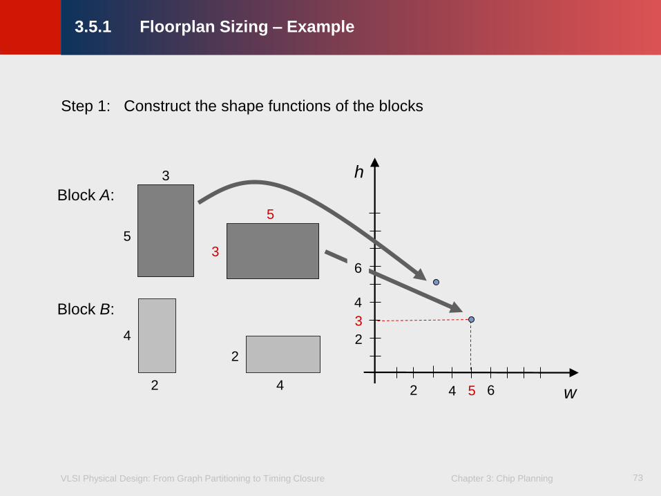
4
2
2
4
Block B:
Block A:
5
5
3
3
Step 1: Construct the shape functions of the blocks
3.5.1 Floorplan Sizing – Example

VLSI Physical Design: From Graph Partitioning to Timing Closure Chapter 3: Chip Planning
© K
LM
H
Lie
nig72
4
2
2
4
Block B:
Block A:
5
5
3
3
3.5.1 Floorplan Sizing – Example
Step 1: Construct the shape functions of the blocks
2
4
h
6
w2 64
5
3
VLSI Physical Design: From Graph Partitioning to Timing Closure Chapter 3: Chip Planning
© K
LM
H
Lie
nig73
4
2
2
4
Block B:
Block A:
5
5
3
3
3.5.1 Floorplan Sizing – Example
Step 1: Construct the shape functions of the blocks
2
4
h
w2 64
6
3
5

VLSI Physical Design: From Graph Partitioning to Timing Closure Chapter 3: Chip Planning
© K
LM
H
Lie
nig74
4
2
2
4
Block B:
Block A:
5
5
3
3
w2 6
2
4
h
4
6
hA(w)
3.5.1 Floorplan Sizing – Example
Step 1: Construct the shape functions of the blocks

VLSI Physical Design: From Graph Partitioning to Timing Closure Chapter 3: Chip Planning
© K
LM
H
Lie
nig75
4
2
2
4
Block B:
Block A:
5
5
3
3
hB(w)
w2 6
2
4
h
4
6
hA(w)
3.5.1 Floorplan Sizing – Example
Step 1: Construct the shape functions of the blocks
VLSI Physical Design: From Graph Partitioning to Timing Closure Chapter 3: Chip Planning
© K
LM
H
Lie
nig76
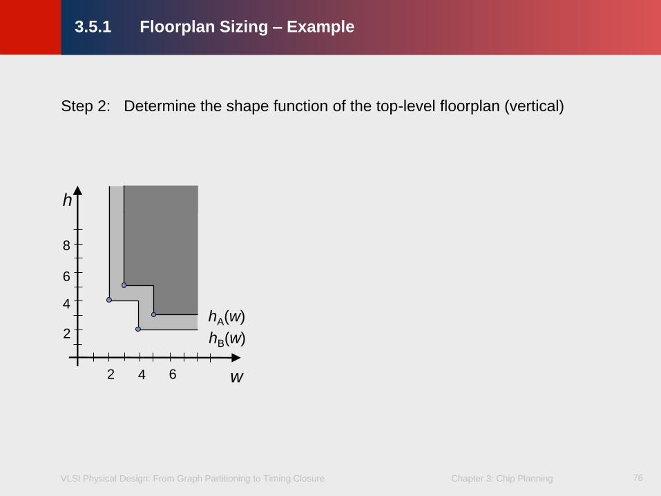
w2 6
2
4
h
4
6
hB(w)
hA(w)
8
3.5.1 Floorplan Sizing – Example
Step 2: Determine the shape function of the top-level floorplan (vertical)

VLSI Physical Design: From Graph Partitioning to Timing Closure Chapter 3: Chip Planning
© K
LM
H
Lie
nig77
w2 6
2
4
h
4
6
hB(w)
hA(w)
8
3.5.1 Floorplan Sizing – Example
Step 2: Determine the shape function of the top-level floorplan (vertical)

VLSI Physical Design: From Graph Partitioning to Timing Closure Chapter 3: Chip Planning
© K
LM
H
Lie
nig78
w2 6
2
4
h
4
6
w2 6
2
4
h
4
6
hB(w)
hA(w)
hB(w)
hA(w)
hC(w)
88
3.5.1 Floorplan Sizing – Example
Step 2: Determine the shape function of the top-level floorplan (vertical)

VLSI Physical Design: From Graph Partitioning to Timing Closure Chapter 3: Chip Planning
© K
LM
H
Lie
nig79
w2 6
2
4
h
4
6
w2 6
2
4
h
4
6
hB(w)
hA(w)
hB(w)
hA(w)
hC(w)
5 x 5
88
3.5.1 Floorplan Sizing – Example
Step 2: Determine the shape function of the top-level floorplan (vertical)

VLSI Physical Design: From Graph Partitioning to Timing Closure Chapter 3: Chip Planning
© K
LM
H
Lie
nig80
w2 6
2
4
h
4
6
w2 6
2
4
h
4
6
hB(w)
hA(w)
hB(w)
hA(w)
hC(w)
3 x 9
4 x 7
5 x 5
88
3.5.1 Floorplan Sizing – Example
Step 2: Determine the shape function of the top-level floorplan (vertical)

VLSI Physical Design: From Graph Partitioning to Timing Closure Chapter 3: Chip Planning
© K
LM
H
Lie
nig81
w2 6
2
4
h
4
6
w2 6
2
4
h
4
6
hB(w)
hA(w)
hB(w)
hA(w)
hC(w)
3 x 9
4 x 7
5 x 5
88
Minimimum top-level floorplan
with vertical composition
3.5.1 Floorplan Sizing – Example
Step 2: Determine the shape function of the top-level floorplan (vertical)

VLSI Physical Design: From Graph Partitioning to Timing Closure Chapter 3: Chip Planning
© K
LM
H
Lie
nig82
w2 6
2
4
h
4
6
w2 6
2
4
h
4
6
hA(w)hB(w) hC(w)hA(w)hB(w)
9 x 3
7 x 4
5 x 5
88
3.5.1 Floorplan Sizing – Example
Step 2: Determine the shape function of the top-level floorplan (horizontal)
Minimimum top-level floorplan
with horizontal composition
VLSI Physical Design: From Graph Partitioning to Timing Closure Chapter 3: Chip Planning
© K
LM
H
Lie
nig83
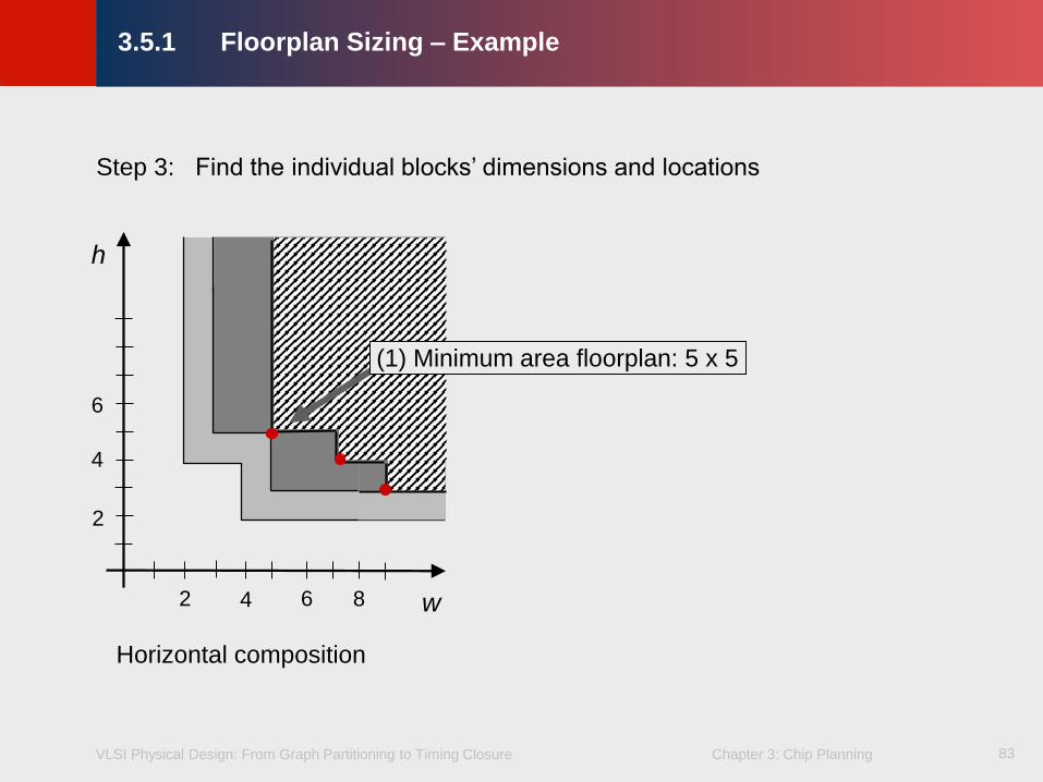
3.5.1 Floorplan Sizing – Example
Step 3: Find the individual blocks’ dimensions and locations
w2 6
2
4
h
4
6
8
(1) Minimum area floorplan: 5 x 5
Horizontal composition

VLSI Physical Design: From Graph Partitioning to Timing Closure Chapter 3: Chip Planning
© K
LM
H
Lie
nig84
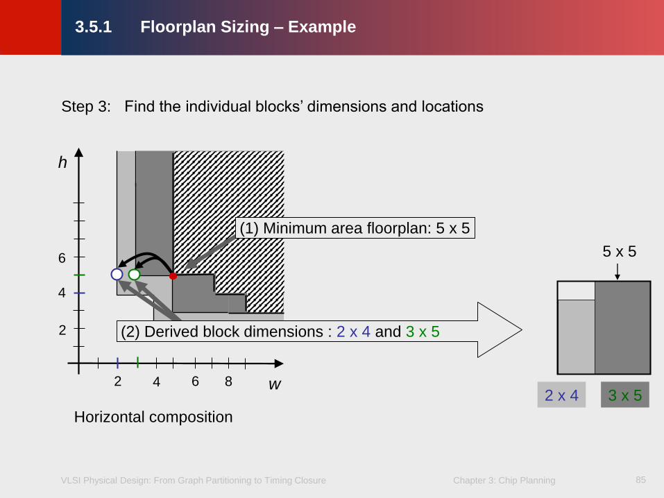
w2 6
2
4
h
4
6
(1) Minimum area floorplan: 5 x 5
(2) Derived block dimensions : 2 x 4 and 3 x 5
8
3.5.1 Floorplan Sizing – Example
Step 3: Find the individual blocks’ dimensions and locations
Horizontal composition
VLSI Physical Design: From Graph Partitioning to Timing Closure Chapter 3: Chip Planning
© K
LM
H
Lie
nig85
2 x 4 3 x 5
5 x 5
3.5.1 Floorplan Sizing – Example
Step 3: Find the individual blocks’ dimensions and locations
w2 6
2
4
h
4
6
(1) Minimum area floorplan: 5 x 5
(2) Derived block dimensions : 2 x 4 and 3 x 5
8
Horizontal composition
86CS 612 – Lecture 4 Mustafa Ozdal
Computer Engineering Department, Bilkent University
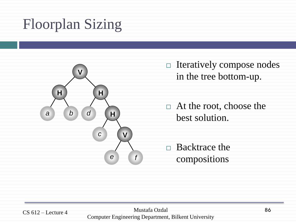
Floorplan Sizing
Iteratively compose nodes
in the tree bottom-up.
At the root, choose the
best solution.
Backtrace the
compositions
H
V
H
d
c
e f
H
V
ba

VLSI Physical Design: From Graph Partitioning to Timing Closure Chapter 3: Chip Planning
© K
LM
H
Lie
nig87
3.5.2 Cluster Growth
w
h
w
h
w
h
a a a
b bc
Growth
direction
2
4
6
4
6
4
© 2
011 S
prin
ger
Verla
g
Iteratively add blocks to the cluster until all blocks are assigned
Only the different orientations of the blocks instead of the shape / aspect ratio
are taken into account
Linear ordering to minimize total wirelength of connections between blocks

VLSI Physical Design: From Graph Partitioning to Timing Closure Chapter 3: Chip Planning
© K
LM
H
Lie
nig88
3.5.2 Cluster Growth – Linear Ordering
New nets have no pins on any block from the partially-constructed ordering
Terminating nets have no other incident blocks that are unplaced
Continuing nets have at least one pin on a block from the partially-constructed
ordering and at least one pin on an unordered block
…
Terminating nets New nets
Continuing nets

VLSI Physical Design: From Graph Partitioning to Timing Closure Chapter 3: Chip Planning
© K
LM
H
Lie
nig89
3.5.2 Cluster Growth – Linear Ordering
Gain of each block m is calculated:
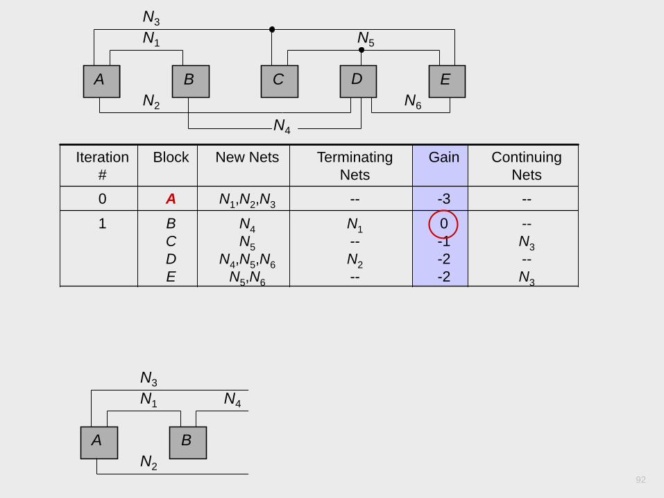
Gainm = (Number of terminating nets of m) – (New nets of m)
The block with the maximum gain is selected to be placed next
A B
N1
N4
GainB = 1 – 1 = 0
VLSI Physical Design: From Graph Partitioning to Timing Closure Chapter 3: Chip Planning
© K
LM
H
Lie
nig90
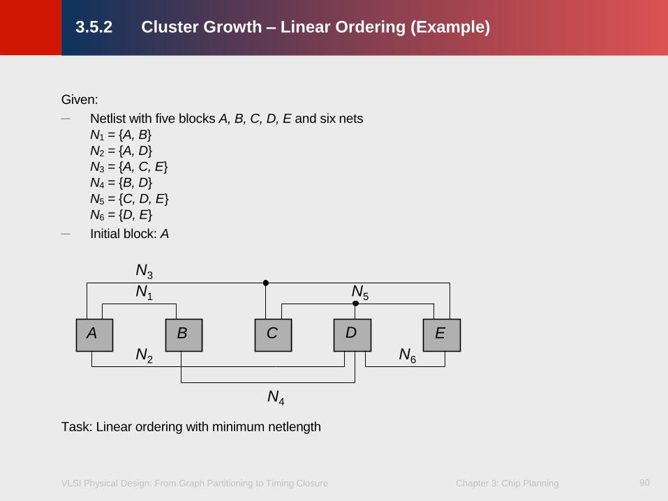
Given:
– Netlist with five blocks A, B, C, D, E and six nets
N1 = {A, B}
N2 = {A, D}
N3 = {A, C, E}
N4 = {B, D}
N5 = {C, D, E}
N6 = {D, E}
– Initial block: A
Task: Linear ordering with minimum netlength
A B C D E
N1
N2
N3
N4
N5
N6
3.5.2 Cluster Growth – Linear Ordering (Example)

VLSI Physical Design: From Graph Partitioning to Timing Closure Chapter 3: Chip Planning
© K
LM
H
Lie
nig91
A B C D E
N1
N2
N3
N4
N5
N6
--2N3,N5--C4
N3,N5
N3,N5
0
1
--
N6
--
--
C
E
3
N3
--
N3
-1
0
-2
--
N2,N4
--
N5
N5,N6
N5,N6
C
D
E
2
--
N3
--
N3
0
-1
-2
-2
N1
--
N2
--
N4
N5
N4,N5,N6
N5,N6
B
C
D
E
1
---3--N1,N2,N3A0
Continuing
Nets
GainTerminating
Nets
New NetsBlockIteration
#
A B D E C
N1
N2
N4 N5
N6
N3
GainA = (Number of terminating nets of A) – (New nets of A)Initial block
VLSI Physical Design: From Graph Partitioning to Timing Closure Chapter 3: Chip Planning
© K
LM
H
Lie
nig92
A B C D E
N1
N2
N3
N4
N5
N6
--2N3,N5--C4
N3,N5
N3,N5
0
1
--
N6
--
--
C
E
3
N3
--
N3
-1
0
-2
--
N2,N4
--
N5
N5,N6
N5,N6
C
D
E
2
--
N3
--
N3
0
-1
-2
-2
N1
--
N2
--
N4
N5
N4,N5,N6
N5,N6
B
C
D
E
1
---3--N1,N2,N3A0
Continuing
Nets
GainTerminating
Nets
New NetsBlockIteration
#
A B D E C
N1
N2
N4 N5
N6
N3

VLSI Physical Design: From Graph Partitioning to Timing Closure Chapter 3: Chip Planning
© K
LM
H
Lie
nig93
A B C D E
N1
N2
N3
N4
N5
N6
--2N3,N5--C4
N3,N5
N3,N5
0
1
--
N6
--
--
C
E
3
N3
--
N3
-1
0
-2
--
N2,N4
--
N5
N5,N6
N5,N6
C
D
E
2
--
N3
--
N3
0
-1
-2
-2
N1
--
N2
--
N4
N5
N4,N5,N6
N5,N6
B
C
D
E
1
---3--N1,N2,N3A0
Continuing
Nets
GainTerminating
Nets
New NetsBlockIteration
#
A B D E C
N1
N2
N4 N5
N6
N3

VLSI Physical Design: From Graph Partitioning to Timing Closure Chapter 3: Chip Planning
© K
LM
H
Lie
nig94
A B C D E
N1
N2
N3
N4
N5
N6
--2N3,N5--C4
N3,N5
N3,N5
0
1
--
N6
--
--
C
E
3
N3
--
N3
-1
0
-2
--
N2,N4
--
N5
N5,N6
N5,N6
C
D
E
2
--
N3
--
N3
0
-1
-2
-2
N1
--
N2
--
N4
N5
N4,N5,N6
N5,N6
B
C
D
E
1
---3--N1,N2,N3A0
Continuing
Nets
GainTerminating
Nets
New NetsBlockIteration
#
© 2
011 S
prin
ger
Verla
g

VLSI Physical Design: From Graph Partitioning to Timing Closure Chapter 3: Chip Planning
© K
LM
H
Lie
nig95
A B D E C
N1
N2
N3
N4 N5
N6
A B C D E
N1
N2
N3
N4
N5
N6
3.5.2 Cluster Growth – Linear Ordering (Example)

VLSI Physical Design: From Graph Partitioning to Timing Closure Chapter 3: Chip Planning
© K
LM
H
Lie
nig96
3.5.2 Cluster Growth – Algorithm
Input: set of all blocks M, cost function C
Output: optimized floorplan F based on C
F = Ø
order = LINEAR_ORDERING(M) // generate linear ordering
for (i = 1 to |order|)
curr_block = order[i]
ADD_TO_FLOORPLAN(F,curr_block,C) // find location and orientation
// of curr_block that causes
// smallest increase based on
// C while obeying constraints
VLSI Physical Design: From Graph Partitioning to Timing Closure Chapter 3: Chip Planning
© K
LM
H
Lie
nig97
3.5.2 Cluster Growth
97
The objective is to minimize the total wirelength of connections blocks
Though this produces mediocre solutions, the algorithm
is easy to implement and fast.
Can be used to find the initial floorplan solutions for iterative algorithms such
as simulated annealing.
Analysis

VLSI Physical Design: From Graph Partitioning to Timing Closure Chapter 3: Chip Planning
© K
LM
H
Lie
nig98
3.5.3 Simulated Annealing
98
Simulated Annealing (SA) algorithms are iterative in nature.
Begins with an initial (arbitrary) solution and seeks to incrementally improve
the objective function.
During each iteration, a local neighborhood of the current solution is
considered. A new candidate solution is formed by a small perturbation of
the current solution.
Unlike greedy algorithms, SA algorithms can accept candidate solutions with
higher cost.
Introduction

VLSI Physical Design: From Graph Partitioning to Timing Closure Chapter 3: Chip Planning
© K
LM
H
Lie
nig99
3.5.3 Simulated Annealing
Solution states
CostInitial solution
Local
optimum Global
optimum

VLSI Physical Design: From Graph Partitioning to Timing Closure Chapter 3: Chip Planning
© K
LM
H
Lie
nig100
3.5.3 Simulated Annealing
100
Definition (from material science): controlled cooling process of high-
temperature materials to modify their properties.
Cooling changes material structure from being highly randomized (chaotic) to
being structured (stable).
The way that atoms settle in low-temperature state is probabilistic in nature.
Slower cooling has a higher probability of achieving
a perfect lattice with minimum-energy
Cooling process occurs in steps
Atoms need enough time to try different structures
Sometimes, atoms may move across larger distances and
create (intermediate) higher-energy states
Probability of the accepting higher-energy states decreases with temperature
What is annealing?

VLSI Physical Design: From Graph Partitioning to Timing Closure Chapter 3: Chip Planning
© K
LM
H
Lie
nig101
3.5.3 Simulated Annealing
101
Generate an initial solution Sinit, and evaluate its cost.
Generate a new solution Snew by performing a random walk
Snew is accepted or rejected based on the temperature T
Higher T means a higher probability to accept Snew if COST(Snew) > COST(Sinit)
T slowly decreases to form the final solution
Boltzmann acceptance criterion, where r is a random number [0,1)
Simulated Annealing
e
COST (Scurr )-COST (Snew )
T > r

VLSI Physical Design: From Graph Partitioning to Timing Closure Chapter 3: Chip Planning
© K
LM
H
Lie
nig102
3.5.3 Simulated Annealing – Algorithm

VLSI Physical Design: From Graph Partitioning to Timing Closure Chapter 3: Chip Planning
© K
LM
H
Lie
nig103
3.5.3 Simulated Annealing – Algorithm
Input: initial solution init_solOutput: optimized new solution curr_sol
T = T0 // initializationi = 0curr_sol = init_solcurr_cost = COST(curr_sol)while (T > Tmin)
while (stopping criterion is not met)i = i + 1(ai,bi) = SELECT_PAIR(curr_sol) // select two objects to perturbtrial_sol = TRY_MOVE(ai,bi) // try small local changetrial_cost = COST(trial_sol)cost = trial_cost – curr_costif (cost < 0) // if there is improvement,
curr_cost = trial_cost // update the cost and curr_sol = MOVE(ai,bi) // execute the move
elser = RANDOM(0,1) // random number [0,1]if (r < e –Δcost/T) // if it meets threshold,
curr_cost = trial_cost // update the cost andcurr_sol = MOVE(ai,bi) // execute the move
T = α ∙ T // 0 < α < 1, T reduction
© 2
011 S
prin
ger
Verla
g

104CS 612 – Lecture 4 Mustafa Ozdal
Computer Engineering Department, Bilkent University
Simulated Annealing – Animation
Source: http://www.biostat.jhsph.edu/~iruczins/teaching/misc/annealing/animation.html

105CS 612 – Lecture 4 Mustafa Ozdal
Computer Engineering Department, Bilkent University
Simulated Annealing - Notes
Practical tuning needed for good results:
How to choose the T values and how to update it?
Should we spend more iterations with high T or low T?
High T: More non-greedy moves accepted
Low T: Accepts mostly greedy moves, but can get stuck
Quality of initial solution should also be considered

106CS 612 – Lecture 4 Mustafa Ozdal
Computer Engineering Department, Bilkent University
Simulated Annealing - Notes
For floorplanning:
Definition of move depends on the representation used
e.g. Polish expression, sequence pair, etc.
Cost evaluation of a move may involve:
packing (e.g. based on horizontal/vertical constraints)
block sizing
wirelength estimation