altera announces the 3.3-v flex 10ka family · 2020. 9. 5. · altera corporation news & views...
TRANSCRIPT

1Altera Corporation News & Views November 1996
FLEX 10KPrice Reductions
See page 4
Newsletter for Altera Customers ◆ Fourth Quarter ◆ November 1996
Altera Announces the 3.3-V FLEX 10KA Family
A-NV-Q496-01
Figure 1. FLEX 10KA I/O CapabilityFLEX 10KA devices have 3.3-V and 5.0-V input tolerance, and can drive both 3.3-Vand 5.0-V devices.
continued on page 3
Altera® announces theFLEX®10KA family of 3.3-Vprogrammable logic devices(PLDs), with projecteddensities up to anunprecedented 250,000 gates.This density combines withsystem speeds over 104MHzand 5.0-V input tolerance to
make the FLEX10KA family the most advanced gatearray replacement available today. The FLEX 10KAfamily directly addresses the need for increasedperformance in larger devices running on low power,and sets a new standard for programmable logic.
FLEX 10KA Offers Enhanced Performance
The FLEX 10KA family will extend the AlteraFLEX10K architecture to a projected 250,000 gates.Based on reconfigurable CMOS SRAM elements, thefamily incorporates all the features necessary toimplement common gate array functions. TheFLEX10KA architecture features fast,efficient embedded array blocks (EABs)containing on-chip RAM and specializedlogic, as well as a logic array for otherlogic functions. This combination of RAMand logic eliminates the tradeoff betweenlogic and memory required by otherarchitectures.
FLEX 10KA devices contain the ClockLockfeature to minimize clock delay and skewand the ClockBoost feature formultiplying the system clock. With thesefeatures, FLEX 10KA devices deliverenhanced performance—even for the mostcomplex functions. For example, an 8-bit,
16-tap finite impulse response (FIR) filter typically runsat 49 MHz in 5.0-V field-programmable gate arrays(FPGAs). However, in the 50,000-gate EPF10K50Adevice, the same filter runs at 104MHz.
Reduced Power Consumption
The amount of power used by a device is a function ofthe power supply voltage and the current used by thedevice. Optimizing a 0.35-micron process for 3.3-Vperformance should reduce the power supply voltageby 34% and the typical current consumption byapproximately 45%. Therefore, the power consumptionof FLEX 10KA devices is expected to be 70% lower thanequivalent 5.0-V devices.
Mixed-Voltage Support
As the migration to 3.3-V devices moves forward,many systems will use both 5.0-V and 3.3-V power. Insome cases, a 5.0-V device will drive the inputs of a3.3-V device. See Figure 1.
3.3-V or5.0-V Input
3.3 V
Logic
GND
3.3 V
GND
FLEX 10KA Device 3.3-V Device
5.0-V Device
3.3-V outputs candrive 3.3-V or 5.0-Vdevices.

2 Altera Corporation News & Views November 1996
Printed on recycled paper.
ContentsFeaturesAltera Announces the 3.3-V FLEX 10KA Family ................ 1Customer Application: MAX 7000 Devices Speed
VMIC to Market ........................................................... 16
Altera NewsNow Available: Altera Digital Library CD-ROM ................ 19Advantages of Carry Chains in FLEX 8000 Devices ......... 20Advantages of Redundancy in High-Density PLDs ......... 21FLEX 10K vs. FPGA Performance ................................... 22The Target Applications Advantage ................................. 23Reed-Solomon CODEC Megafunction ............................. 24
Devices & ToolsAltera Reduces FLEX 10K Prices up to 50% .....................4New Devices Added to the FLEX 10K Family ..................... 4Altera Introduces New FLEX 8000 Packages .................... 4New MAX 9000 Package Options ..................................... 5MAX 7000S Availability .................................................... 5MAX 7000S: The Fastest Devices with ISP ....................... 5Altera Migrates EPM7192E to 0.65-Micron Process ......... 5Product Transitions .......................................................... 5MAX+PLUS II 7.1 To Ship In December ........................... 6
Altera, AHDL, AMPP, BitBlaster, ByteBlaster, Classic, ClockLock, ClockBoost, FastTrack, FLASHlogic, FLEX, FLEX 10K,FLEX 10KA, FLEX8000, FLEX 8000A, FLEX DSP, MAX 9000, MAX 7000, MAX 7000E, MAX7000S, MAX 5000, MAX,MAX+PLUS, MAX+PLUSII, MegaCore, Altera Megafunction Partners Program, PLDasm, and specific device designationsare trademarks and/or service marks of Altera Corporation in the United States and other countries. Altera acknowledgesthe trademarks of other organizations for their respective products or services mentioned in this document, specifically:SuperBGA is a registered trademark of Amkor/Anam. Verilog is a registered trademark of Cadence Design Systems. DataI/O is a registered trademark of Data I/O Corporation. FISP is a registered trademark of Object Oriented Hardware.Synopsys is a registered trademark of Synopsys, Inc. Viewlogic is a registered trademark of Viewlogic Systems. Alteraproducts are protected under numerous U.S. and foreign patents and pending applications, maskwork rights, andcopyrights. Altera warrants performance of its semiconductor products to current specifications in accordance withAltera’s standard warranty, but reserves the right to make changes to any products and services at any time withoutnotice. Altera assumes no responsibility or liability arising out of the application or use of any information, product, orservice described herein except as expressly agreed to in writing by Altera Corporation. Altera customers are advised toobtain the latest version of device specifications before relying on any published information and before placing orders forproducts or services.
Forward-looking statements in this newsletter are made pursuant to the safe harbor provisions ofthe Private Securities Litigation Reform Act of 1995. Investors are cautioned that all forward-looking statements involve risks and uncertainty, including without limitation risks of dependenceon third-party wafer suppliers, intellectual property rights and litigation, market acceptance ofand demand for the Company‘s products as well as general market conditions, competition andpricing, and development of technology and manufacturing capabilities. Please refer to Altera‘sSecurities and Exchange Commission filings, copies of which are available from Altera withoutcharge, for further information.
Copyright © 1996 Altera Corporation. All rights reserved.
For information about thisnewsletter, or to submitquestions, contact:
Erica Heidinger, PublisherCraig Lytle, Technical Editor2610 Orchard ParkwaySan Jose, CA 95134-2020Tel: (408) 894-7000Fax: (408) 954-0348E-mail: [email protected]
®
Fast Fourier Transform Function Available in December ... 6High-Performance BGA Package Now Available ................ 7Discontinued Devices ....................................................... 8
Technical ArticlesCreating Optimized, Fixed-Coefficient 2-D Video
Convolvers .................................................................... 9Designing with MegaCore Functions .............................. 10Using the genmem Utility ............................................... 11Clock Management with ClockLock & ClockBoost .......... 12Evaluating Power in Altera Devices ................................. 14Questions & Answers ..................................................... 18
In Every IssueNew Altera Publications .................................................... 8Altera Device Selection Guide ......................................... 25Data I/O Programming Support ...................................... 28Software Utilities ............................................................ 28Programming Hardware Compatibility ............................ 29Current Software Versions .............................................. 29How to Request Altera Publications ................................ 30How to Access Altera ...................................................... 30Fax Response Form ........................................................ 31

3Altera Corporation News & Views November 1996
Because PLDs are often the interface between thedevices on a board, high-performance PLDs with theability to support the electrical requirements of both5.0-V and 3.3-V devices provide the ideal interface formixed-voltage systems. Altera gives designersmaximum flexibility by including 5.0-V input tolerancein 3.3-V FLEX 10K and all FLEX 10KA devices.Additionally, FLEX 10KA devices can drive 5.0-V TTLlogic levels.
Technology Advantages
FLEX 10KA devices are built on a 0.35-micron, quad-layer metal SRAM process that enables the smallestpossible die size, improves yields, and lowers costs.This process is optimized for 3.3-V operation, whichensures low power consumption without sacrificingperformance. Figure2 compares the 0.5-micron triple-layer metal die to the 0.35-micron quad-layer metalEPF10K50A die.
State-of-the-Art Packaging
The performance and process improvements inFLEX10KA devices are complemented by modernpackaging technology that accommodates the higherlead counts in larger devices. FLEX 10KA devices areavailable in high-pin-count ball-grid array (BGA)packages, which greatly reduce the problem of bentleads, as well as in traditional quad flat pack packages.Pin migration will be supported, reducing costs forsystem engineers who wantto place their design in alarger device without havingto change device pin-outs orboard layout. No other PLDoffers the combination ofdensity, performance,packaging, and pricing foundin the FLEX10KA family.
Software Support
The FLEX10KA family willbe supported by Altera’sMAX+PLUS® II developmentsystem. Altera also provides
Figure 2. EPF10K50 Die Comparison
MegaCore functions that are pretested and optimizedfor Altera architectures as MAX+PLUSII migrationproducts. Altera currently offers a microperipheralfunction library and is planning to release fast Fouriertransform (FFT) and peripheral componentinterconnect (PCI) functions with MAX+PLUS IIversion7.1. Future function will include more digitalsignal processing (DSP) and networking functions. Formore information on the MegaCore design flow, see“Designing with MegaCore Functions” on page 10.
Available Now
3.3-V EPF10K50V devices on a 0.35-micron, triple-layermetal process are available now. Members of theFLEX10KA family, including the EPF10K250A with250,000 gates of programmable logic, will be availableby the end of 1997. Table 1 provides a summary ofFLEX 10KA devices. For more information, contactAltera Customer Marketing.
Altera Announces the 3.3-V FLEX 10KA Familycontinued from page 1
0.5-Micron Triple-Layer Metal 0.35-Micron Quad-Layer Metal
Table 1. FLEX 10KA Devices
Device Typical Density (Gates)
EPF10K250A 250,000
EPF10K130A 130,000
EPF10K100A 100,000
EPF10K70A 70,000
EPF10K50A 50,000
EPF10K40A 40,000
EPF10K30A 30,000
EPF10K20A 20,000
EPF10K10A 10,000
Feature
4 Altera Corporation News & Views November 1996
Devices& T O O L S
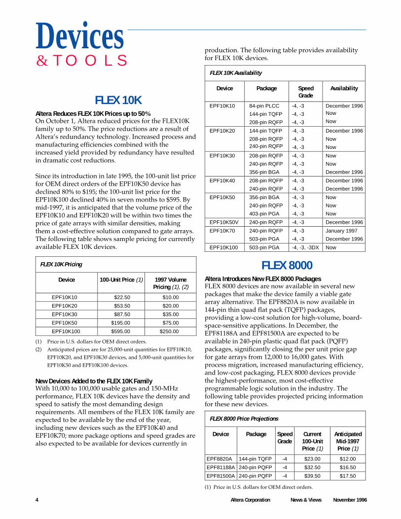
FLEX 10KAltera Reduces FLEX 10K Prices up to 50%On October 1, Altera reduced prices for the FLEX10Kfamily up to 50%. The price reductions are a result ofAltera’s redundancy technology. Increased process andmanufacturing efficiencies combined with theincreased yield provided by redundancy have resultedin dramatic cost reductions.
Since its introduction in late 1995, the 100-unit list pricefor OEM direct orders of the EPF10K50 device hasdeclined 80% to $195; the 100-unit list price for theEPF10K100 declined 40% in seven months to $595. Bymid-1997, it is anticipated that the volume price of theEPF10K10 and EPF10K20 will be within two times theprice of gate arrays with similar densities, makingthem a cost-effective solution compared to gate arrays.The following table shows sample pricing for currentlyavailable FLEX 10K devices.
(1) Price in U.S. dollars for OEM direct orders.(2) Anticipated prices are for 25,000-unit quantities for EPF10K10,
EPF10K20, and EPF10K30 devices, and 5,000-unit quantities forEPF10K50 and EPF10K100 devices.
New Devices Added to the FLEX 10K FamilyWith 10,000 to 100,000 usable gates and 150-MHzperformance, FLEX 10K devices have the density andspeed to satisfy the most demanding designrequirements. All members of the FLEX 10K family areexpected to be available by the end of the year,including new devices such as the EPF10K40 andEPF10K70; more package options and speed grades arealso expected to be available for devices currently in
production. The following table provides availabilityfor FLEX 10K devices.
(1) Price in U.S. dollars for OEM direct orders.
FLEX 10K Pricing
Device 100-Unit Price (1) 1997 VolumePricing (1), (2)
EPF10K10 $22.50 $10.00
EPF10K20 $53.50 $20.00
EPF10K30 $87.50 $35.00
EPF10K50 $195.00 $75.00
EPF10K100 $595.00 $250.00
FLEX 8000 Price Projections
Device Package SpeedGrade
Current100-UnitPrice (1)
Anticipated Mid-1997Price (1)
EPF8820A 144-pin TQFP -4 $23.00 $12.00
EPF81188A 240-pin PQFP -4 $32.50 $16.50
EPF81500A 240-pin PQFP -4 $39.50 $17.50
FLEX 10K Availability
Device Package SpeedGrade
Availability
EPF10K10 84-pin PLCC
144-pin TQFP
208-pin RQFP
-4, -3
-4, -3
-4, -3
December 1996Now
Now
EPF10K20 144-pin TQFP
208-pin RQFP240-pin RQFP
-4, -3
-4, -3
-4, -3
December 1996
Now
Now
EPF10K30 208-pin RQFP
240-pin RQFP
356-pin BGA
-4, -3
-4, -3
-4, -3
Now
Now
December 1996
EPF10K40 208-pin RQFP
240-pin RQFP
-4, -3
-4, -3
December 1996
December 1996
EPF10K50 356-pin BGA
240-pin RQFP
403-pin PGA
-4, -3
-4, -3
-4, -3
Now
Now
Now
EPF10K50V 240-pin RQFP -4, -3 December 1996
EPF10K70 240-pin RQFP
503-pin PGA
-4, -3
-4, -3
January 1997
December 1996
EPF10K100 503-pin PGA -4, -3, -3DX Now
FLEX 8000Altera Introduces New FLEX 8000 PackagesFLEX 8000 devices are now available in several newpackages that make the device family a viable gatearray alternative. The EPF8820A is now available in144-pin thin quad flat pack (TQFP) packages,providing a low-cost solution for high-volume, board-space-sensitive applications. In December, theEPF81188A and EPF81500A are expected to beavailable in 240-pin plastic quad flat pack (PQFP)packages, significantly closing the per unit price gapfor gate arrays from 12,000 to 16,000 gates. Withprocess migration, increased manufacturing efficiency,and low-cost packaging, FLEX 8000 devices providethe highest-performance, most cost-effectiveprogrammable logic solution in the industry. Thefollowing table provides projected pricing informationfor these new devices.

5Altera Corporation News & Views November 1996
Devices & Tools
continued on page 6
MAX® 9000New MAX 9000 Package OptionsNew package options for the MAX 9000 family aresummarized below:
■ EPM9560 devices in 208-pin power quad flat pack(RQFP) packages are now shipping as replace-ments for existing 208-pin ceramic quad flat pack(CQFP) packages. These new devices are form, fit,and functionally equivalent to EPM9560 devices in208-pin CQFP packages.
■ EPM9400 devices are now shipping in 84-pinplastic J-lead chip carrier (PLCC) packages.
■ EPM9560 devices in 356-pin ball-grid array (BGA)packages, the first BGA package for the MAX 9000family, will be available in December.
MAX 7000MAX 7000S AvailabilityAltera has expanded production for MAX7000Sdevices. EPM7128S and EPM7192S are currently inproduction. EPM7256S and EPM7064S devices areavailable as engineering samples; production quantitiesare anticipated to be available in December andJanuary, respectively. MAX7000S device availability isshown below.
MAX 7000S: The Fastest Devices with ISPFollowing the performance leadership of the MAX 7000product family, MAX 7000S devices offer the highestperformance with in-system programmability (ISP) on
Notes:(1) This process transition will not result in any changes to data
sheet parameters or ordering codes.(2) Devices manufactured on the 0.65-micron process must be
programmed with new programming adapters.
Note:
(1) Statistics in this table were obtained from the world-wide websites of Xilinx, Lattice, and AMD.
Altera Migrates EPM7192E to 0.65-Micron ProcessIn January 1997, Altera expects to ship EPM7192Edevices fabricated on a 0.65-micron process. Evaluationpackets for qualification are available—containingreliability data, device samples, and documentation—from your local Altera representative.
MAX 5000 & ClassicProduct TransitionsAltera is migrating existing MAX 5000 and Classicdevices from a 0.8-micron process to a 0.65-micronprocess. Evaluation packets (containing device samplesand documentation) are available from your localAltera sales representative. The table below outlinesthe migration schedule:
Product Migration Schedule
Description (1) Reference Device Date
MAX 5000 devices PCN 9407 EPM5032 Q1 1997
fabricated on a ADV 9515 EPM5064 Q2 1997
0.65-micron process ADV 9606 EPM5128 Complete
Note (2) EPM5130 May 1, 1997
EPM5192 October 1, 1996
Classic devices PCN 9510 EP6xx Complete
fabricated on a 0.65- ADV 9607 EP9xx September 1, 1996
micron process EP18xx March 1, 1997
the market today (see the table below). MAX 7000Sdevices offer a performance of up to 125 MHz for a 16-bit loadable, up/down counter.
Comparison of Devices with ISP Note (1)
Feature AlteraEPM7128S
XilinxXC95108
LatticeispLSI2128
AMDMACH 5-128
MemoryElements
EEPROM FLASH EECMOS EEPROM
Macrocells 128 108 128 128
tPD (ns) 7.5 10 10 7.5
Package 160-pin
PQFP
160-pin
PQFP
176-pin
TQFP
160-pin
PQFP
Availability Now Now Now Q4 1996
MAX 7000S Availability
Device Package Speed Grade ProjectedAvailability
EPM7192S 160-pin PQFP -10, -15 Now
EPM7128S 160-pin PQFP -7, -10, -15 Now
100-pin PQFP -7, -10, -15 Now
100-pin TQFP -7, -10, -15 December 1996
EPM7256S 160-pin PQFP -10, -15 December 1996
208-pin RQFP -10, -15 December 1996
EPM7064S 44-pin PLCC -7, -10 January 1997
44-pin TQFP -7, -10 Q1 1997
100-pin PQFP -7, -10 January 1997
EPM7032S 44-pin PLCC -5, -6, -7, -10 Q1 1997
44-pin TQFP -5, -6, -7, -10 Q1 1997
EPM7096S 100-pin PQFP -7, -10, -15 Q2 1997
100-pin TQFP -7, -10, -15 Q2 1997
160-pin PQFP -7, -10, -15 Q2 1997
EPM7160S 100-pin TQFP -7, -10, -15 Q2 1997
84-pin PLCC -7, -10, -15 Q2 1997
6 Altera Corporation News & Views November 1996
Devices & Tools
Devices & Toolscontinued from page 5
New Altera programming adapters are required toprogram the 0.65-micron devices. Altera will exchangeexisting EPM5032, EPM5064, and EPM5130programming adapters for new adapters for free. Thesenew adapters are backwards-compatible and supportall existing die revisions. The table below lists theexisting MAX 5000 adapters that can be exchanged fornew adapters. Altera has already completed anexchange program for EPM5128 and EPM5192programming adapters.
Contact Altera’s Customer Service Department or yourlocal Altera sales representative for more information.
MAX+PLUS II
MAX+PLUS II 7.1 To Ship In DecemberAltera is expanding offerings of devices and packagesat a rapid pace. By December of this year, Altera plansto add a total of seven new device/packages to theFLEX 10K and MAX 9000 families. MAX+PLUS II,version 7.1 will be available in December to supportthese new devices.
In addition to new device support, MAX+PLUS IIversion 7.1 provides improved VHDL capability.Message location is improved, and support foradditional structures and VHDL ‘93 syntax areprovided. Altera is also improving timing models forSynopsys, which will result in better timing-drivensynthesis results within Synopsys tools.
Altera’s software maintenance program ensures thatyou will have the most up-to-date support for Altera’s
devices, as well as the latest features and capabilities.For more information on purchasing a maintenanceagreement, contact your local Altera representative.
Fast Fourier Transform Function Available in DecemberAltera will be releasing the fast Fourier transform (FFT)MegaCore function as a migration product toMAX+PLUS II version 7.1. With this new function,Altera continues to provide the broadest support fordigital signal processing (DSP) applications. DSPmegafunctions optimized for FLEX devices provideflexibility that is critical to high-performanceapplications such as radio frequency (RF) ratecommunications systems for cable and wirelessnetworks.
Fastest FFT Solution AvailableThe fully parameterized FFT megafunction performssignificantly faster than DSP processors andsubstantially faster than previously availableprogrammable logic implementations. In the past,high-performance FFT functions were available only asexpensive DSP standard product and multiprocessorsolutions, or as inflexible ASIC solutions. WithFLEX10K devices, designers have the option of usingembedded array blocks (EABs) as on-chip RAM.Table1 shows the FFT function performance for AlteraFLEX 10K devices using EABs.
MAX 5000 Replacement Adapters
Existing Adapter New Adapter
PLED5032
PLMD5032
PLEJ5032
PLM5032
PLES5032
PLMD5032A
PLMD5032A
PLMJ5032A
PLMJ5032A
PLMS5032A
PLEJ5064
PLMJ5064
PLMJ5064A
PLMJ5064A
PLEG5130
PLEJ5130
PLMJ5130
PLEQ5130
PLMQ5130
PLMG5130A
PLMJ5130A
PLMJ5130A
PLMQ5130A
PLMQ5130A
Parameterized for Ease of UseDesigners can optimize the FFT megafunction forspecific applications by customizing a variety ofparameters. The FFT length can be specified as anypower of 2 and the data width and the twiddle width
Table 2 provides FFT function performance for AlteraFLEX 10K devices using standard synchronous SRAM.
Table 1. FFT Performance & Device Utilization with EABs
Length(Points)
Precision Memory Size(LEs)
Speed(µs)
512 16 Data, 8 Twiddle Single 2,000 186
512 8 Data, 8 Twiddle Dual 1,150 94
512 12 Data, 12 Twiddle Dual 1,970 94
512 16 Data, 16 Twiddle Single 2,993 190
Table 2. FFT Performance & Utilization with External RAM
Length(Points)
Precision Memory Size(LEs)
Speed
1,024 16 Data, 16 Twiddle Single 2,993 411 µs
1,024 16 Data, 16 Twiddle Dual 2,993 207 µs
32 K 16 Data, 16 Twiddle Dual 3,100 9.8 ms

7Altera Corporation News & Views November 1996
Devices & Tools
Ball-grid array (BGA) packages are low-profile, high-power packages with performance benefits overtraditional surface-mount packages. A BGA packagecontains an integrated circuit that is mounted to asmall circuit board. Input and output pins are replacedwith solder balls, which are arranged in a matrix on thebottom of the board. The final device is then soldereddirectly to printed circuit boards in a process similar tostandard surface-mount technology.
BGA packages have advanced substrate designs withintegrated copper heat sinks for enhanced thermalperformance. BGA packages also utilize provenassembly practices and materials to ensure highreliability and performance. Available in a variety ofball (I/O) counts and standard JEDEC body sizes, BGApackages are supported by an industry infrastructurethat includes contract manufacturing.
To ensure the highest level of reliability, the latest BGApackage from Amkor/Anam (named SuperBGA) usesthe newest materials and process technologies.Incorporating the die and I/O on the same side of thepackage improves signal integrity and speed. Theenhanced multilayer package delivers even greaterperformance by increasing speed, decreasinginductance, and reducing noise.
The SuperBGA package couples high-performancewith dramatic size and weight refinements. A typical35 × 35 mm SuperBGA package has a mounted heightof less than 1.4 mm and weighs 7.0 grams.
High-Performance BGA Package Now Available
The increased performance and space savings of theSuperBGA package make it ideal for high-density,high-performance devices. Therefore, Altera hasteamed with Amkor/Anam to offer FLEX10K devicesin the SuperBGA package.
The EPF10K50 in a 35-mm, 356-pin BGA packageprovides the following advantages over traditionalpackages:
■ 52 more user I/O pins than the 304-pin thermallyenhanced quad flat pack (QFP)
■ Weight of approximately 26 grams■ Footprint of 42.6 mm2
The new BGA package provides a size savings of over32% with 17% more user I/O pins.
can be configured to any positive number. The FFTfunction permits 1 or 2 data bank memoryarchitectures. This flexibility ensures that the compiledmegafunction is optimized for both area and speed tosupport specific customer applications.
AMPP SupportTo encourage the development of large DSPapplications, Altera will provide the low-level,architecture-optimized information in the FFT
MegaCore function to partners in the AlteraMegafunction Partners Program (AMPP) forintegration into more complex functions. AMPPpartners are also working on FFT implementations.
Pricing and AvailabilityThe FFT MegaCore function is priced at $7,995 and willbe available as a migration product for MAX+PLUS IIversion 7.1 in December 1996. The ordering code forthe library is PLSM-FFT.
8 Altera Corporation News & Views November 1996
In recent months, Altera has announced that variousproducts will be discontinued (see the table below).Altera distributes advisories (ADVs) and productdiscontinuance notices (PDNs) that provideinformation on discontinued devices. To obtain a copyof a specific ADV or PDN, contact your local Alterasales representative. Selected ADVs, PDNs, and a
complete listing of discontinued devices are alsoavailable on Altera’s world-wide web site athttp://www.altera.com. Rochester Electronics, an after-market supplier, offers support for many discontinuedAltera products. Contact Rochester Electronics at(508)462-9332 for more information.
Discontinued Devices
New Altera PublicationsNew Altera publications are available from AlteraLiterature Services, and Altera Express. Individualdocuments are available on the Altera world-wideweb site. Document part numbers are shown initalics.
■ Altera Digital Library P-CD-ADL-01Provides a complete electronic collection ofcurrent Altera technical literature for all Alteradevice families and development software. Amultimedia presentation highlighting theFLEX10K family is also provided.
■ Microperipheral MegaCore Library Data BookA-DB-MEGA-01Provides data sheets for the a8237 DMAcontroller, a6402 UART, a16450 UART, a8251
Devices & Tools
UART, a6850 UART, and a8255 programmableperipheral interface adapter MegaCore functions.The microperipheral library is a migrationproduct for MAX+PLUS II version 7.1 and higher.
■ Solution Brief 1: Reed-Solomon CODEC A-SB-001-01Gives a description, including parameters, of theReed-Solomon CODEC megafunction from ObjectOriented Hardware.
■ Solution Brief 2: FIR Filter A-SB-002-01Provides a description, block diagram, andparameters for the FIR filter megafunction fromIntegrated Silicon Solutions, Ltd.
■ Solution Brief 3: Biquad IIR Filter A-SB-003-01Gives a description, block diagram, andparameters for the biquad IIR filter megafunctionfrom Integrated Silicon Solutions, Ltd.
Discontinued Device Ordering Codes
Device Family Device Last OrderDate
Last ShipmentDate
Reference
FLEX 8000 Military products (all 883B, DESC, and military temperature grades) 10/31/96 12/31/96 PDN 9513PDN 9517
MAX 7000 Military products (all 883B, DESC, and military temperature grades) 10/31/96 12/31/96 PDN 9513
FLASHlogic EPX740 (all packages, temperature grades, and speed grades) 3/31/97 9/30/97 PDN 9516
MAX 5000 Military EPM5130W device 10/31/96 12/31/96 PDN 9513
Selected MAX 5000 ordering codes 9/30/96 12/31/96 ADV 9609
EPM5016 (all packages, temperature grades, and speed grades) 3/31/97 9/30/97 PDN 9516
Classic Military products (all 883B, DESC, and military temperature grades) 10/31/96 12/31/96 PDN 9513
EP220, EP224, EP312, EP324 (all packages, temperature grades,and speed grades)
3/31/97 9/30/97 PDN 9516
Selected EP9xx ordering codes 9/30/96 12/31/96 ADV 9608
Selected EP18xx ordering codes 3/31/97 6/30/97 ADV 9608
Function-Specific
EPS448, EPC1213 military (all 883B, DESC, and military temperaturegrades)
10/31/96 12/31/96 PDN 9513PDN 9517
EPS448, EPS464 (all commercial and industrial temperature grades;military devices have earlier last order and last shipment dates)
3/31/97 9/30/97 PDN 9516
9Altera Corporation News & Views November 1996
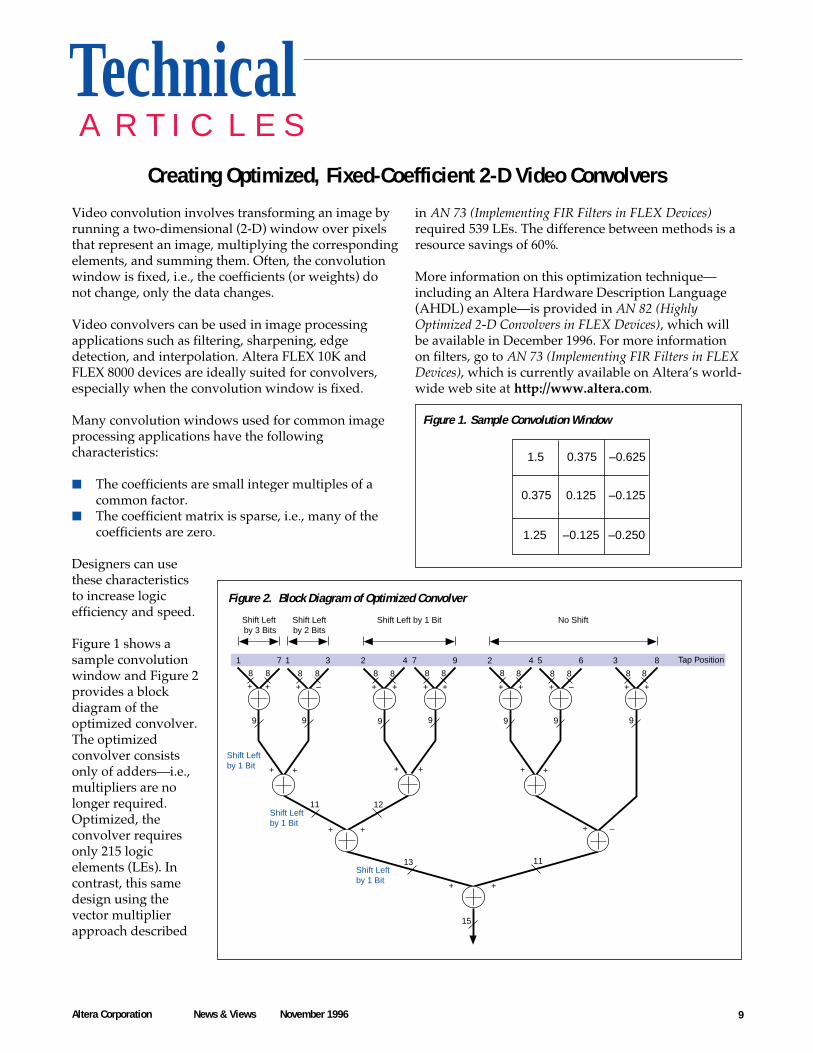
Video convolution involves transforming an image byrunning a two-dimensional (2-D) window over pixelsthat represent an image, multiplying the correspondingelements, and summing them. Often, the convolutionwindow is fixed, i.e., the coefficients (or weights) donot change, only the data changes.
Video convolvers can be used in image processingapplications such as filtering, sharpening, edgedetection, and interpolation. Altera FLEX 10K andFLEX 8000 devices are ideally suited for convolvers,especially when the convolution window is fixed.
Many convolution windows used for common imageprocessing applications have the followingcharacteristics:
■ The coefficients are small integer multiples of acommon factor.
■ The coefficient matrix is sparse, i.e., many of thecoefficients are zero.
Designers can usethese characteristicsto increase logicefficiency and speed.
Figure 1 shows asample convolutionwindow and Figure 2provides a blockdiagram of theoptimized convolver.The optimizedconvolver consistsonly of adders—i.e.,multipliers are nolonger required.Optimized, theconvolver requiresonly 215 logicelements (LEs). Incontrast, this samedesign using thevector multiplierapproach described
Creating Optimized, Fixed-Coefficient 2-D Video Convolvers
in AN 73 (Implementing FIR Filters in FLEX Devices)required 539 LEs. The difference between methods is aresource savings of 60%.
More information on this optimization technique—including an Altera Hardware Description Language(AHDL) example—is provided in AN 82 (HighlyOptimized 2-D Convolvers in FLEX Devices), which willbe available in December 1996. For more informationon filters, go to AN 73 (Implementing FIR Filters in FLEXDevices), which is currently available on Altera’s world-wide web site at http://www.altera.com.
Figure 2. Block Diagram of Optimized Convolver
Figure 1. Sample Convolution Window
TechnicalA R T I C L E S
1.5
0.375
1.25 –0.125
0.125
0.375 –0.625
–0.125
–0.250
11
15
13
12
1 7 31 2 974 2 4 5 6 3 8 Tap Position
11
+ –
8 8 8 8 8 8 8 8 8 8 8 8 8 8
9 9 9 9 9 9 9
Shift Leftby 1 Bit
Shift Leftby 1 Bit
Shift Leftby 1 Bit
+ + + – + + + + + ++ – + +
Shift Left by 3 Bits
Shift Leftby 2 Bits
Shift Left by 1 Bit No Shift
+ +
++
+ +++ ++
10 Altera Corporation News & Views November 1996
Designing with MegaCore Functions
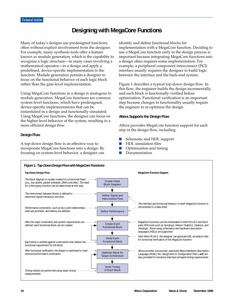
Figure 1. Top-Down Design Flow with MegaCore Functions
Many of today’s designs use predesigned functions,often without explicit involvement from the designer.For example, many synthesis tools offer a featureknown as module generation, which is the capability torecognize a logic structure—in many cases involving amathematical operator—in a design and apply apredefined, device-specific implementation to thefunction. Module generation permits a designer tofocus on the functional behavior of each logic blockrather than the gate-level implementation.
Using MegaCore functions in a design is analogous tomodule generation. MegaCore functions are commonsystem-level functions, which have predesigned,device-specific implementations that can beinstantiated in a design and functionally simulated.Using MegaCore functions, the designer can focus onthe higher-level behavior of the system, resulting in amore efficient design flow.
Design Flow
A top-down design flow is an effective way toincorporate MegaCore functions into a design. Byfocusing on system-level behavior, a designer can
identify and define functional blocks forimplementation with a MegaCore function. Deciding touse a MegaCore function early in the design process isimportant because integrating MegaCore functions intoa design often requires some implementation. Forexample, a peripheral component interconnect (PCI)interface usually requires the designer to build logicbetween the interface and the back-end system.
Figure 1 describes a typical top-down design flow. Inthis flow, the engineer builds the design incrementally,and each block is functionally verified beforeoptimization. Functional verification is an importantstep because changes in functionality usually requirethe engineer to re-optimize the design.
Altera Supports the Design Flow
Altera provides MegaCore function support for eachstep in the design flow, including:
■ Schematic and HDL support■ HDL simulation files■ Optimization and timing■ Documentation
Technical Articles
Define Performance
Create InitialBlock Diagram
Create EachFunctional Block
Define Signal andInterconnect Flow
Verify EachFunctional Block
Optimize Block forTarget Architecture
Verify Timingof Each Block
The block diagram is usually created on a functional basis(e.g., bus arbiter, packet scheduler, DMA controller). The needfor a third-party function can be determined at this step.
The interconnect between blocks is defined todetermine signal interaction and flow.
Performance constraints, such as bus cycle relationships,interrupt priorities, and latency are defined.
After the major constraints and system requirements aredefined, each functional block can be created.
Each block is verified against a test bench that reflects thefunctional requirement for the block.
After functional verification, the design is optimized to meetarea and performance constraints.
Timing checks are performed using static timingmeasurements.
Top-Down Design Flow MegaCore Function Support
MegaCore functions can be instantiated in MAX+PLUS II and third-party EDA tools such as Synopsys, Mentor Graphics, Cadence, andViewlogic. Flows using schematics and hardware descriptionlanguages (HDLs) are supported.
The interface and functional behavior of each MegaCore function isdocumented in a data sheet.
With MAX+PLUS II, the designer can generate HDL simulation filesfor functional verification of the MegaCore function.
Altera provides a structured, optimized Altera Hardware DescriptionLanguage (AHDL) file. Assignment & Configuration Files (.acf) arealso provided for functions that have stringent timing requirements.

11Altera Corporation News & Views November 1996
Technical Articles
Altera has optimized MegaCore functions for Alteradevices. Therefore, designers can use MegaCorefunctions without modifications, ensuring that thefunction’s optimization is preserved. Designers cancustomize functions as needed using a variety ofparameters. For example, designers can specify thelength, data width, and twiddle width of the fastFourier transform (FFT) MegaCore function.
Conclusion
A design flow with MegaCore functions is similar tothe one used by gate array designers today. A top-down design strategy helps identify opportunities touse MegaCore functions early in the process, leavingthe designer free to focus on system behavior.
You can use Synopsys tools and Altera’s genmemutility to create designs for FLEX 10K embedded arrayblocks (EABs) that implement RAM and ROM. Thegenmem utility produces three output files:
■ Functional simulation model—genmem can createboth VHDL and Verilog HDL simulation models tosupport pre-synthesis and post-synthesis, pre-place-and-route functional simulation.
■ Library timing model—This model contains timinginformation that can be used by Synopsys tools fortiming-driven synthesis and timing estimation.
■ Component Declaration—For VHDL, genmemcreates a file containing a Component Declarationfor the element to be instantiated. This ComponentDeclaration is required by synthesis and simulationtools. When using Verilog HDL, the moduledeclaration found in the functional simulationmodel can be instantiated.
How to Use genmem
First, generate the necessary output .v and .lib files forthe memory function you desire. For example, to createoutput files for dual-port RAM that is 64 words deepand 8 bits wide in Verilog HDL, type the following at aUNIX command prompt:
genmem csdpram 64x8 -verilog
The genmem utility will produce the filecsdp_ram_64x8.v for simulation and the filecsdp_ram_64x8.lib for synthesis.
Using genmem for Synthesis
Perform the steps below to use the utility for synthesis:
1. Instantiate the RAM. For example, in Verilog HDL,include the following in your design:
csdp_ram_64x8 <RAM Name> (DataA,DataB, AddressA, AddressB, WEa,WEb, Clock, Clockx2, QA, QB, Busy);
Using the genmem Utility
You can obtain the port names from MAX+PLUS IIHelp or the genmem functional simulation model.
2. Add the .lib file to the library of your choice. Forexample, to add the RAM from Step 1 to theFLEX10K library ( flex10k.db), type the followingat the Synopsys tool command line:
read -f db flex10k.db 9update_lib flex10k csdp_ram_64x8.lib 9write_lib flex10k -o flex10k.db 9
3. Apply the dont_touch property to the RAM sothat the Synopsys tools will pass this instance ofthe RAM into an EDIF file as a hollow-bodycomponent. During compilation, MAX+PLUSIIwill map the RAM to a dual-port RAM with adepth of 64 and a width of 8.
You do not need to read in the simulation model filefor synthesis.
Using genmem for Functional Simulation(Before Place & Route)
The genmem utility creates a functional simulationmodel that describes the behavior of the RAM. To usethe simulation model, read it into the simulation toolwith the rest of the functional design description andthe test bench, and then simulate the design.
Using genmem for Functional Simulation(After Place & Route)
You do not need to use the genmem utility for post-place and route simulation. MAX+PLUS II includes allof the necessary information in the VHDL andVerilogHDL output files.

12 Altera Corporation News & Views November 1996
Clock Management with ClockLock & ClockBoost
Technical Articles
As programmable logic devices (PLDs) increase indensity, on-device clock distribution becomesincreasingly important for device performance. To helpmanage clocking in Altera high-density PLDs, Alteraprovides the ClockLock and ClockBoost features. TheClockLock feature incorporates a phase-locked loop(PLL) with a balanced clock tree to minimize on-deviceclock delay and skew. The ClockBoost feature providesclock multiplication, which increases clock frequenciesby as much as four times the incoming clock rate,improving system bandwidth. For example, a 100-MHzdesign can be fed by a 50-MHz clock, which is thendoubled in the Altera device. Clock multiplicationsimplifies printed circuit board (PCB) designs becausethe clock path on the PCB does not require thedistribution of a high-speed clock signal.
Clock Delay & Skew
The delay from the clock pin to a register can besignificant—especially for large devices—and candecrease both on- and off-device performance. Theequation for calculating the pin-to-pin clock-to-outputtime is shown below.
tCO = tCLOCK + tSKEW + tREGISTER_CO + tOUTPUT
The tCLOCK and tSKEW parameters account for asignificant portion of the total clock-to-output delay inlarge devices. Therefore, reducing the tCLOCK delay willminimize the clock-to-output time. A large clock delayalso decreases the performance of the signal drivinginto the device because it can cause positive hold timesfor the input register. To create a zero hold time, abuilt-in delay is added to the data path. However, thisadded data delay increases the setup time for theregister. The equations for setup and hold times areshown below.
tSU = tREGISTER_SU + tDATA - tCLOCK - tSKEWtH = tCLOCK + tSKEW + tREGISTER_H - tDATA
Clock skew—the difference between clock delays todifferent registers—can also increase the setup time. Toensure a zero hold time, the built-in delay is increasedto account for the longest clock delay to any register.However, increased data delay also increases the setuptime of other registers with shorter clock delays. TheClockLock and ClockBoost features help mitigate clockdelay and skew.
ClockLock: Faster System Performance
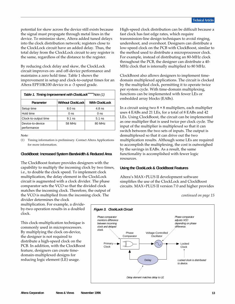
The ClockLock feature minimizes clock delay by usinga PLL, which locks onto the incoming clock andgenerates a clock signal that leads the incoming clock.The difference between the incoming clock at the pinand the ClockLock-generated clock approximates thedelay from the ClockLock circuitry to the register,minimizing the apparent delay from the clock pin tothe register. Figure 1 shows a schematic of the clockdistribution circuit.
Figure 2 shows the waveform for the ClockLockcircuitry.
External connections or devices are not required andtight control of timing is maintained because the entireClockLock circuit is implemented within the PLD. TheClockLock circuit uses a phase comparator to comparethe incoming clock to an internally generated delayedclock. The delay from the voltage-controlled oscillator(VCO) models the delay of the internally generatedclock to the registers in the device. The phasecomparator controls the VCO that drives the clockthroughout the device. See Figure 3.
The ClockLock circuit generates a clock signal withminimal delay from the clock pin to the registers. The
Figure 2. Waveform of ClockLock-Generated Clock
Figure 1. ClockLock Clock Distribution
Clock
D Q
D Q
ClkLock
ClockDelay
ClockLock ClockClock at Pin Clock at Register
Clock at Pin
ClockLock Clock
Clock at Register
Effective clock delay is small.
13Altera Corporation News & Views November 1996
Technical Articles
Figure 3. ClockLock Circuit
potential for skew across the device still exists becausethe signal must propagate through metal lines in thedevice. To minimize skew, Altera added tuned delaysinto the clock distribution network; registers close tothe ClockLock circuit have an added delay. Thus, thetotal delay from the ClockLock circuit to any register isthe same, regardless of the distance to the register.
By reducing clock delay and skew, the ClockLockcircuit improves on- and off-device performance andmaintains a zero hold time. Table 1 shows theimprovement in setup and clock-to-output times for anAltera EPF10K100 device in a -3 speed grade.
Note:
(1) Timing information is preliminary. Contact Altera Applicationsfor more information.
ClockBoost: Increased System Bandwidth & Reduced Area
The ClockBoost feature provides designers with thecapability to multiply the incoming clock by two times,i.e., to double the clock speed. To implement clockmultiplication, the delay element in the ClockLockcircuit is augmented with a clock divider. The phasecomparator sets the VCO so that the divided clockmatches the incoming clock. Therefore, the output ofthe VCO is multiplied from the incoming clock. Thedivider determines the clockmultiplication. For example, a divide-by-two operation results in a doubledclock.
This clock-multiplication technique iscommonly used in microprocessors.By multiplying the clock on-device,the designer is not required todistribute a high-speed clock on thePCB. In addition, with the ClockBoostfeature, designers can create time-domain-multiplexed designs forreducing logic element (LE) usage.
continued on page 15
High-speed clock distribution can be difficult because afast clock has fast edge rates, which requiretransmission-line design techniques to avoid ringing,undershoot, and overshoot. Designers can distribute alow-speed clock on the PCB with ClockBoost, similar tothe method used to distribute a microprocessor clock.For example, instead of distributing an 80-MHz clockthroughout the PCB, the designer can distribute a 40-MHz clock that is internally multiplied to 80 MHz.
ClockBoost also allows designers to implement time-domain multiplexed applications. The circuit is clockedby the multiplied clock, permitting it to operate twiceper system cycle. With time-domain multiplexing,functions can be implemented with fewer LEs orembedded array blocks (EABs).
In a circuit using two 8 × 8 multipliers, each multiplieruses 4 EABs and 21 LEs, for a total of 8 EABs and 42LEs. Using ClockBoost, the circuit can be implementedas one multiplier that is used twice per clock cycle. Theinput of the multiplier is multiplexed so that it canswitch between the two sets of inputs. The output isdemultiplexed so that it can drive out the twomultiplication results. Although some LEs are requiredto accomplish the multiplexing, the cost is outweighedby the savings in EABs. As a result, the samefunctionality is accomplished with fewer logicresources.
Using the ClockLock & ClockBoost Features
Altera’s MAX+PLUS II development softwaresimplifies the use of the ClockLock and ClockBoostcircuits. MAX+PLUS II version 7.0 and higher provides
Table 1. Timing Improvement with ClockLock Note (1)
Parameter Without ClockLock With ClockLock
Setup time 8.0 ns 4.8 ns
Hold time 0 ns 0 ns
Clock-to-output time 9.1 ns 5.1 ns
Device-to-deviceperformance
58 MHz 80 MHz
PhaseComparator
Voltage-ControlledOscillator
Delay
PrimaryClock
LockedClock
Delay element matches delay to LE.
Phase comparatoradjusts VCOdepending on phasedifference.
Phase comparatormonitors differencebetween incomingclock and delayedclock.
Locked clock is distributedto device.

14 Altera Corporation News & Views November 1996
Design:_______________________ Device:_______________________
Estimating the Power Consumption of the Application
Internal Power Calculation
FLEX 10K & FLEX 8000 Devices
Standby current (ICCSTANDBY)
Coefficient for ICC calculation. See the appropriate device family data sheet for this value.
Highest clock frequency of the design (fMAX)
Logic elements used (N)
Average ratio of logic cells toggling (tog LC) at each clock (typically 0.125)
Total internal current (ICCINT) ICCINT
= ICCSTANDBY + K × fMAX × N × tog LC
Convert to mA (i.e., divide by 1,000)
Total internal power (PINT) PINT = VCC × ICCINT
MAX 9000 & MAX 7000 Devices
Coefficients for ICC calculation. See the appropriate device family
data sheet for these values.
Number of macrocells used with turbo bit on (MCTON)
Number of macrocells used with turbo bit off (MCTOFF)
Number of macrocells in the design (MCUSED = MCTON + MCTOFF)
Highest clock frequency of the design (fMAX)
Average ratio of logic cells toggling (tog LC) at each clock (typically 0.125)
Total internal current (ICCINT)
ICCINT = (A × MCTON) + (B × MCTOFF) + (C × MCUSED × fMAX × tog LC)
Total internal power (PINT) PINT = VCC × ICCINT
ICCSTANDBY =
K =
fMAX =
N =
tog LC =
ICCINT =
ICCINT =
PINT =
______________mA
______________µA/MHz × LE
______________MHz
______________
______________
______________µA
______________mA
______________ mW
A =
B =
C =
MCTON =
MCTOFF =
MCUSED =
fMAX =
tog LC =
ICCINT =
PINT =
______________
______________
______________
______________
______________
______________
______________MHz
______________
______________mA
______________mW
Technical Articles
A critical element of system reliability is the capacity ofelectronic devices to safely dissipate the heat generatedduring operation. The thermal characteristics of acircuit depend on the device and package used, theoperating temperature, the operating current, and thesystem’s ability to dissipate heat.
You should complete a power evaluation early in thedesign process to help identify potential heat-relatedproblems in the system and to prevent the system fromexceeding the device’s maximum allowed junctiontemperature.
The actual power dissipated by most applications issignificantly lower than the power the package can
Evaluating Power in Altera Devices
dissipate. However, a thermal analysis should beperformed for all projects. To perform a powerevaluation, follow these steps:
■ Estimate the power consumption of theapplication.
■ Calculate the maximum power allowed for thedevice and package.
■ Compare the estimated power and maximumpower values.
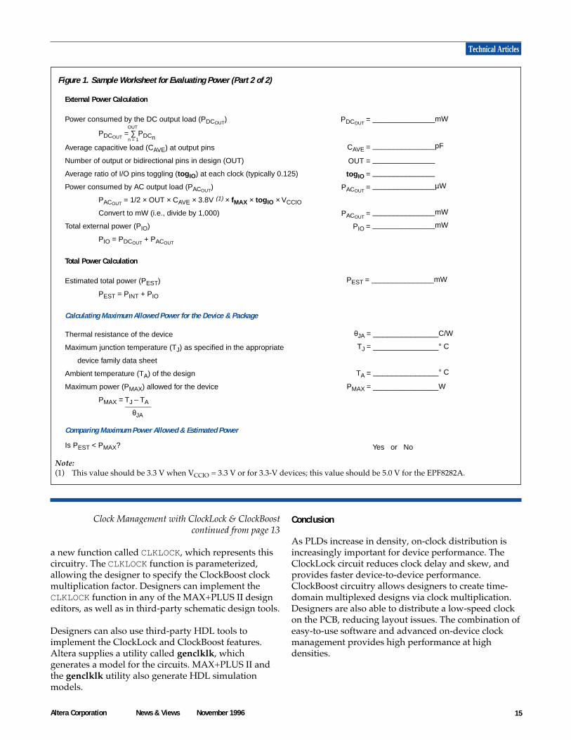
The following figure shows a worksheet that you canuse for evaluating power. For more information, referto AN 74 (Evaluating Power for Altera Devices) in the1996 Data Book.
Figure 1. Sample Worksheet for Evaluating Power (Part 1 of 2)
15Altera Corporation News & Views November 1996
Figure 1. Sample Worksheet for Evaluating Power (Part 2 of 2)
a new function called CLKLOCK, which represents thiscircuitry. The CLKLOCK function is parameterized,allowing the designer to specify the ClockBoost clockmultiplication factor. Designers can implement theCLKLOCK function in any of the MAX+PLUS II designeditors, as well as in third-party schematic design tools.
Designers can also use third-party HDL tools toimplement the ClockLock and ClockBoost features.Altera supplies a utility called genclklk, whichgenerates a model for the circuits. MAX+PLUS II andthe genclklk utility also generate HDL simulationmodels.
Conclusion
As PLDs increase in density, on-clock distribution isincreasingly important for device performance. TheClockLock circuit reduces clock delay and skew, andprovides faster device-to-device performance.ClockBoost circuitry allows designers to create time-domain multiplexed designs via clock multiplication.Designers are also able to distribute a low-speed clockon the PCB, reducing layout issues. The combination ofeasy-to-use software and advanced on-device clockmanagement provides high performance at highdensities.
Clock Management with ClockLock & ClockBoostcontinued from page 13
Note:(1) This value should be 3.3 V when VCCIO = 3.3 V or for 3.3-V devices; this value should be 5.0 V for the EPF8282A.
Calculating Maximum Allowed Power for the Device & Package
Thermal resistance of the device
Maximum junction temperature (TJ) as specified in the appropriate
device family data sheet
Ambient temperature (TA) of the design
Maximum power (PMAX) allowed for the device
PMAX = TJ – TA
θJA
θJA =
TJ =
TA =
PMAX =
______________C/W
______________° C
______________° C
______________W
_______
External Power Calculation
Power consumed by the DC output load (PDCOUT)
PDCOUT = ∑ PDCn
Average capacitive load (CAVE) at output pins
Number of output or bidirectional pins in design (OUT)
Average ratio of I/O pins toggling (tog IO) at each clock (typically 0.125)
Power consumed by AC output load (PACOUT)
PACOUT = 1/2 × OUT × CAVE × 3.8V (1) × fMAX × tog IO × VCCIO
Convert to mW (i.e., divide by 1,000)
Total external power (PIO)
PIO = PDCOUT + PACOUT
Total Power Calculation
Estimated total power (PEST)
PEST = PINT + PIO
PEST = _______________mW
Yes or No
OUT
n = 1
PDCOUT =
CAVE =
OUT =
tog IO =
PACOUT =
PACOUT =
PIO =
_______________mW
_______________pF
_______________
_______________
_______________µW
_______________mW
_______________mW
Comparing Maximum Power Allowed & Estimated Power
Is PEST < PMAX?
Technical Articles
16 Altera Corporation News & Views November 1996
MAX 7000 Devices Speed VMIC to Market
“There is no other way todevelop a board designthis fast without the use ofPLDs.”— Ed Danford,
Design Manager, VMIC
CustomerAPPLICATION
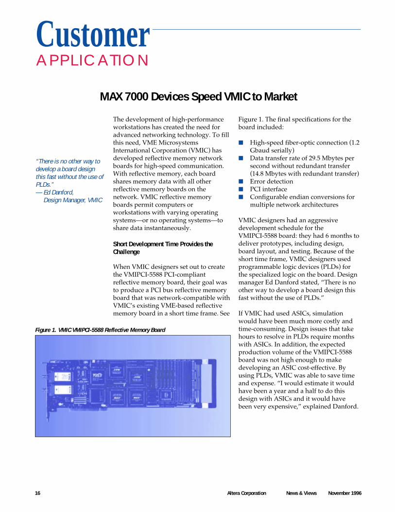
Figure 1. VMIC VMIPCI-5588 Reflective Memory Board
The development of high-performanceworkstations has created the need foradvanced networking technology. To fillthis need, VME MicrosystemsInternational Corporation (VMIC) hasdeveloped reflective memory networkboards for high-speed communication.With reflective memory, each boardshares memory data with all otherreflective memory boards on thenetwork. VMIC reflective memoryboards permit computers orworkstations with varying operatingsystems—or no operating systems—toshare data instantaneously.
Short Development Time Provides theChallenge
When VMIC designers set out to createthe VMIPCI-5588 PCI-compliantreflective memory board, their goal wasto produce a PCI bus reflective memoryboard that was network-compatible withVMIC’s existing VME-based reflectivememory board in a short time frame. See
Figure 1. The final specifications for theboard included:
■ High-speed fiber-optic connection (1.2Gbaud serially)
■ Data transfer rate of 29.5 Mbytes persecond without redundant transfer(14.8 Mbytes with redundant transfer)
■ Error detection■ PCI interface■ Configurable endian conversions for
multiple network architectures
VMIC designers had an aggressivedevelopment schedule for theVMIPCI-5588 board: they had 6 months todeliver prototypes, including design,board layout, and testing. Because of theshort time frame, VMIC designers usedprogrammable logic devices (PLDs) forthe specialized logic on the board. Designmanager Ed Danford stated, “There is noother way to develop a board design thisfast without the use of PLDs.”
If VMIC had used ASICs, simulationwould have been much more costly andtime-consuming. Design issues that takehours to resolve in PLDs require monthswith ASICs. In addition, the expectedproduction volume of the VMIPCI-5588board was not high enough to makedeveloping an ASIC cost-effective. Byusing PLDs, VMIC was able to save timeand expense. “I would estimate it wouldhave been a year and a half to do thisdesign with ASICs and it would havebeen very expensive,” explained Danford.
17Altera Corporation News & Views November 1996
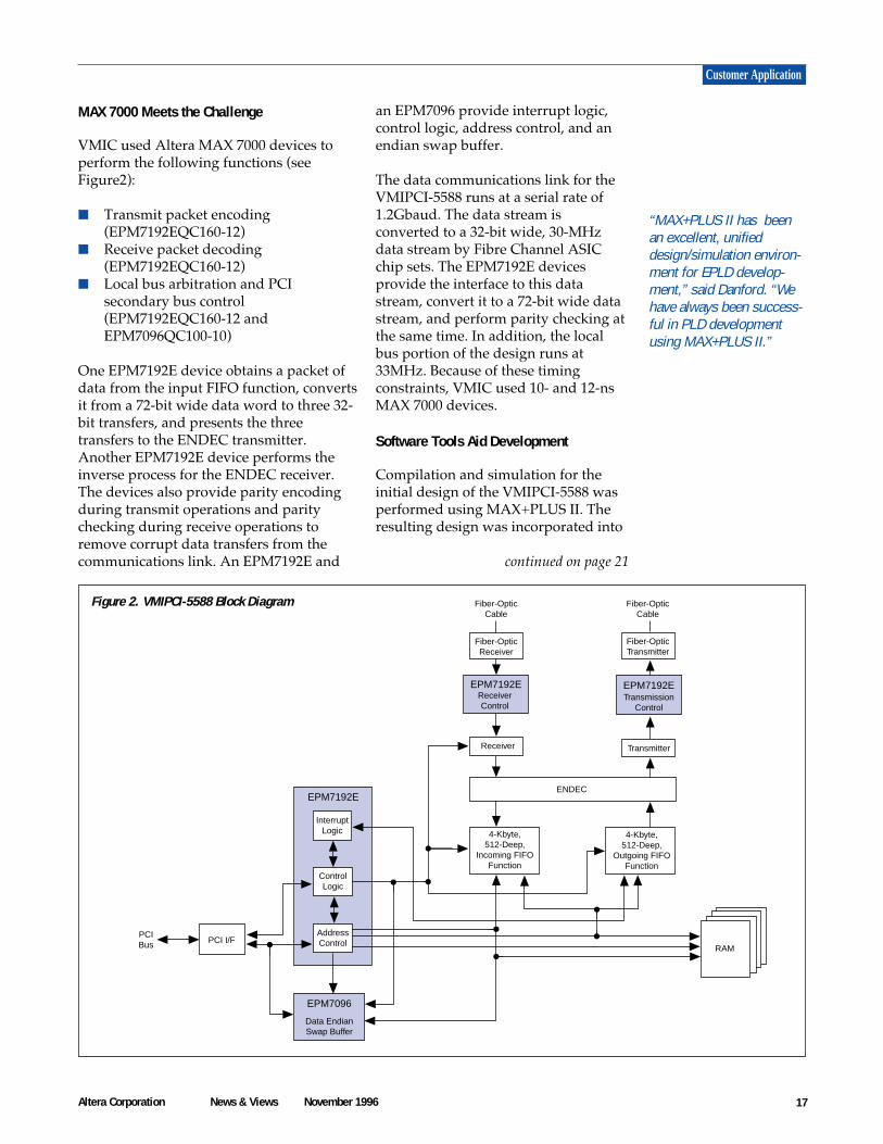
Figure 2. VMIPCI-5588 Block Diagram
“MAX+PLUS II has beenan excellent, unifieddesign/simulation environ-ment for EPLD develop-ment,” said Danford. “Wehave always been success-ful in PLD developmentusing MAX+PLUS II.”
Customer Application
MAX 7000 Meets the Challenge
VMIC used Altera MAX 7000 devices toperform the following functions (seeFigure2):
■ Transmit packet encoding(EPM7192EQC160-12)
■ Receive packet decoding(EPM7192EQC160-12)
■ Local bus arbitration and PCIsecondary bus control(EPM7192EQC160-12 andEPM7096QC100-10)
One EPM7192E device obtains a packet ofdata from the input FIFO function, convertsit from a 72-bit wide data word to three 32-bit transfers, and presents the threetransfers to the ENDEC transmitter.Another EPM7192E device performs theinverse process for the ENDEC receiver.The devices also provide parity encodingduring transmit operations and paritychecking during receive operations toremove corrupt data transfers from thecommunications link. An EPM7192E and
an EPM7096 provide interrupt logic,control logic, address control, and anendian swap buffer.
The data communications link for theVMIPCI-5588 runs at a serial rate of1.2Gbaud. The data stream isconverted to a 32-bit wide, 30-MHzdata stream by Fibre Channel ASICchip sets. The EPM7192E devicesprovide the interface to this datastream, convert it to a 72-bit wide datastream, and perform parity checking atthe same time. In addition, the localbus portion of the design runs at33MHz. Because of these timingconstraints, VMIC used 10- and 12-nsMAX 7000 devices.
Software Tools Aid Development
Compilation and simulation for theinitial design of the VMIPCI-5588 wasperformed using MAX+PLUS II. Theresulting design was incorporated into
continued on page 21
EPM7192E
Fiber-OpticCable
Fiber-OpticCable
ENDEC
Fiber-OpticTransmitter
Fiber-OpticReceiver
4-Kbyte,512-Deep,
Outgoing FIFOFunction
4-Kbyte,512-Deep,
Incoming FIFOFunction
Data EndianSwap Buffer
EPM7096
EPM7192E
Receiver
ControlLogic
AddressControl
InterruptLogic
PCI I/FRAM
PCIBus
EPM7192E
Transmitter
ReceiverControl
TransmissionControl

18 Altera Corporation News & Views November 1996
Questions& A N S W E R S
QWhen I try to compile my design for theEPF10K10T144, MAX+PLUS II version 7.0 won’t
create a Programmer Object File (.pof). What’s wrong?
AYou must enter the password 4RT5XN forMAX+PLUS II version 7.0 to create a POF for the
EPF10K10T144.
QWhen configuring FLEX devices, how long does ittake nSTATUS to go high after nCONFIG is driven
high?
ADuring configuration, the FLEX device canreceive configuration data after nCONFIG is
driven high, nSTATUS is released, and nSTATUS ispulled high by the pull-up resistor. The delay betweennCONFIG and nSTATUS being released depends onhow nCONFIG is driven. If nCONFIG is tied to VCC andthe FLEX device configures immediately upon power-up, nSTATUS will stay low for 100 ms after power-up.If nCONFIG is reset after the power is stabilized, thetime difference is approximately 10 µs. See thefollowing figure.
Q I am using the mixed-voltage I/O capability of Alteradevices. In what order should I power-up the VCC for
the I/O and the internal VCC? Is there any time limit on thepower-up sequence?
AFor most Altera devices with mixed-voltage I/O,the power-up sequence does not matter and no
time limit exists; you can power-up the internal VCCwhile leaving the I/O VCC alone for a long period oftime without harming the device.
FLEX 8000 devices configured in active mode with aserial configuration EPROM are an exception to thisrule. The order of power-up does not matter. However,if the internal VCC is powered first, the I/O VCC mustbe powered within 100 ms to ensure successfulconfiguration. If the I/O VCC is powered before theinternal VCC, pins with design-controlled tri-statebuffers will drive out.
QWhy do I receive an error during in-systemprogramming when a non-Altera device is in the JTAG
chain?
AWhen you include non-Altera devices in a JTAGchain, you must specify JTAG information for the
non-Altera device in MAX+PLUS II by performing thefollowing steps:
1. In the MAX+PLUS II Programmer, choose Multi-Device JTAG Chain Setup (JTAG menu).
2. Choose JTAG Device Attributes. The JTAGDevice Attributes dialog box is displayed.
3. Enter the name, instruction register length,boundary scan length, and JTAG ID code for thenon-Altera device. Choose OK.
When you choose OK, the information you enteredabout the non-Altera device is stored in a file namedjtaginfo.crf. Usually, this file is stored in the maxplus2directory for PCs or the /usr/maxplus2/common/directory for workstations.
QWhen I try to install MAX+PLUS II on my PC, Ireceive the following error:
Install caused a general protection fault in
module installw.bin
What’s wrong?
AYou need to include your CD-ROM drive in thepath of your autoexec.bat file. For example:
path = C:\DOS; <CD-ROM drive letter>
Waveforms for nCONFIG & nSTATUS
nCONFIG
nSTATUS
nCONFIG
nSTATUS
100 ms
10 µs
nCONFIG Is Tied to VCC
nCONFIG Is Pulsed Low after Power Stabilizes
19Altera Corporation News & Views November 1996
Questions & Answers
Q I just installed the latest version of MAX+PLUS II onmy PC. When I try to run the software, I receive errors
that MAX+PLUS II cannot find several .dll files. How can Iget those files?
AIf you received this error after performing a fullinstallation (i.e., not a custom installation), verify
that you have a minimum of 16 MBytes of physicalRAM and 16MBytes of permanent virtual RAM. Also,if you are running memory management software suchas QEMM, turn the software off while you areinstalling MAX+PLUS II.
If you received this error after performing a custominstallation of MAX+PLUS II, you may not haveinstalled all of the files that MAX+PLUS II requires.You can install these missing files separately. Forexample, if you receive an error that you are missingthe j2p.dll file, you can extract the file from theMAX+PLUS II installation CD-ROM by performing thefollowing steps:
1. At a DOS command prompt, go to the maxplus2directory.
2. Type in the following command:
<CD-ROM drive>:\pc\maxplus2\maxzip -x
<CD-ROM drive>:\pc\prog\p.azp j2p.dll 9
The j2p.dll file will be extracted from the CD-ROMinto the current directory.
Q I’m creating a VHDL design for an Altera deviceusing Synopsys tools. How do I instantiate global
buffers?
AYou can use a Component Instantiation Statementto insert an instance of a primitive or
macrofunction. For example:
COMPONENT global
PORT (a_in : IN STD_LOGIC;
(a_out : OUT STD_LOGIC);
END COMPONENT;
BEGIN
u1 : global
PORT MAP (clk, gclk)
END;
QWhen I try to bring an EDIF file into MAX+PLUSIIfrom a third-party tool, I receive the following error:
Can’t find design file <filename>.
What’s wrong?
AIf you do not have the most recent Alteralibraries installed, you may receive this error.
Verify that you are using current Altera libraries—MAX+PLUS II version 7.0 is available now, and version7.1 will be available in December 1996.
Q I created a design for the EPX780 device, but I wouldlike to use the EPX880 instead. How can I compile the
design and program the EPX880?
AYou can compile the design for the EPX880device using Altera’s PLDshell Plus software
version5.1. This software is available for free on theAltera world-wide web site at http://www.altera.com.Program the EPX880 device as you would the EPX780device, using the FLASHlogic Download Cable(ordering code PL-FLDLC). You can also use theByteBlaster and MAX+PLUS II or PLDshell Plus toprogram EPX880 devices.
Now Available:Altera Digital Library CD-ROM
The Altera Digital Library contains an electronicversion of all current Altera technical literature,including updates and supplements released afterprinting. The CD-ROM also provides a multimediapresentation on the FLEX 10K family. To obtain acopy of the Altera Digital Library, contact AlteraLiterature Services at (888) 3-ALTERA or sende-mail to [email protected].

20 Altera Corporation News & Views November 1996
Carry chains are high-speed data paths that connectadjacent logic elements (LEs) without using otherinterconnect resources. The carry chain operation inprogrammable logic architecture has a significantimpact on the performance of arithmetic functions in adevice. The FLEX 8000 carry chain provides a very fast(less than 1 ns) carry-forward function between LEs,which can implement the sum of a single-bit adder andcarry-generation logic within a single LE. See Figure 1.Optimizing speed and efficiency, the FLEX 8000 carrychain provides twice the performance and uses 50%fewer logic resources than competing low-cost FPGAs.
In contrast, some FPGAs are less efficient because eachlogic cell only calculates a half sum; an adjacent logiccell must be used to complete the addition. SeeFigure2. Because the critical path in an FPGA adder orcounter includes the additional logic cell required toimplement the full-add operation, an additional logicdelay is incurred, which results in significantly slowerarithmetic performance.
While some FPGAs require an additional logic cell toinitialize the carry chain, the FLEX 8000 LE caninitialize its own carry chain. Where some FPGAsrequire two logic cells to implement the full addition,the FLEX 8000 architecture implements the sameoperation in a single LE. Implementing an n-bit counterrequires 2n+1 logic cells in some FPGAs and only nLEs in FLEX 8000 devices. Similarly in adders, an n-bitadder requiring 2n+1 logic cells in some FPGAs,requires only n+1 LEs in FLEX 8000 devices. Thisresource efficiency is illustrated in Figure 3.
In the FLEX 8000 architecture, the carry-in signal froma lower-order bit moves forward into the higher-orderbit via the carry chain, feeding into the look-up table(LUT) and the next portion of the carry chain. Thisfeature allows the FLEX 8000 architecture to implementhigh-speed counters and adders of arbitrary width.Using the MAX+PLUS II Compiler, carry chains can becreated automatically during design processing;designers can also insert carry chain logic manuallyduring design entry.
Advantages of Carry Chains in FLEX 8000 Devices
Figure 1. FLEX 8000 Carry Chain
Figure 2. FPGA Carry Chain
AlteraN E W S
+
+
+
+
LE
LE
LE
LE
SUM3
SUM2
SUM1
SUM0
A3B3
A3B3
A3B3
A3B3
LE can initializeits own carry-in.
0
Full sum and carry isimplemented in one LE.
Logic Cell
Logic Cell
Logic Cell
Logic Cell
Logic Cell
Logic Cell
Logic Cell
Logic Cell
Logic Cell
0
SUM3
SUM2
SUM1
SUM0
A3B3
A3B3
A3B3
A3B3
Additional logic cell requiredfor initial carry-in.
Computes sum fromcarry and half-sum.
Carry
Carry
Carry

21Altera Corporation News & Views November 1996
Altera News
Figure 3. Resource Efficiency of FLEX 8000 vs. FPGAsCarry chains make FLEX 8000 devices the optimalsolution for arithmetic-intensive applications such asdigital signal processing. The architecture of theFLEX8000 device allows tradeoffs between speed,resource utilization, and easy fitting. FLEX 8000devices provide twice the performance of comparableFPGAs and save the designer money by providing theflexibility to fit a given design into a smaller FLEX 8000device.
The semiconductor manufacturing process demandscleanliness because it only takes one microscopicdust particle to damage a transistor. The transistor isthe basic building block in any device and even onefailing transistor can cause an entire device to fail.To eliminate transistor failure, semiconductormanufacturers have added redundant circuitry tohigh-density devices. Redundant circuits are “spare”functional blocks that can be substituted fordefective blocks, without affecting the functionalityor timing of a device.
With redundancy, manufacturers can save devicesthat were traditionally discarded due to defects.
Therefore, redundancy results in higher yields andlower costs. For example, without redundancy, 16-Mbit and 64-Mbit DRAM would not be economicallyfeasible. Redundancy significantly improves yieldsand reduces costs for these devices, making themcompetitive.
Because redundancy requires a slightly larger die, itis most effective in high-density devices. Altera’spatented redundancy is used in the FLEX10K,FLEX8000, and MAX 9000 device families. For moreinformation on redundancy in Altera devices,contact Altera Customer Marketing.
Advantages of Redundancy in High-Density PLDs
a schematic board design, which was used to lay outthe board. During testing, as problems were found inthe design, the VMIC designers performed additionalsimulation and made changes to the PLD design asnecessary. Simulation was used to confirm fixes beforethe devices were reprogrammed.
VMIC used the Altera Hardware Description Language(AHDL) to create the designs for the MAX 7000devices. The design team found that the easy-to-useMAX+PLUS II software simplified their task ofdetermining if a device was fast enough to perform thedesired logic task. “MAX+PLUS II has been an
excellent, unified design/simulation environment forEPLD development,” said Danford. “We have alwaysbeen successful in PLD development usingMAX+PLUS II.”
Altera Provides Time-to-Market Advantage
With PLDs, many design errors can be corrected bysimple reprogramming without having to changeboard layout. This process saves time and money whendeveloping new products. “Time-to-market is veryimportant to us, so we will choose the products that getus there as quickly as possible,” Danford said. UsingAltera’s MAX 7000 devices and MAX+PLUS IIsoftware, VMIC was able to meet their aggressive timeschedule: the VMIPCI-5588 reflective memory boardgot to market on time.
MAX 7000 Devices Speed VMIC to Marketcontinued from page 17
80
60
40
20
0
8 16 24 32
FPGA
FLEX 8000
Numberof LEs
Number of Bits

22 Altera Corporation News & Views November 1996
Altera News
FLEX 10K vs. FPGA Performance
The Altera FLEX 10K programmable logic device (PLD)family combines the flexibility of programmable logicand the density and efficiency of embedded gatearrays. FLEX 10K devices contain both a logic arrayand an embedded array that can be used for RAM,ROM, or complex logic functions. With the addedcapability of the embedded array, the FLEX 10K familyoffers up to 100,000 gates—a breakthrough inprogrammable logic—and satisfies the densityrequirements of over 80% of gate array design starts(source: Dataquest). Altera’s new FLEX 10KA familywill provide up to 250,000 gates. Refer to “AlteraAnnounces the 3.3-V FLEX 10KA Family” on page 1 formore information.
FLEX 10K Provides Faster Performance
The FLEX 10K family features the largest device in theprogrammable logic industry, and also provides fasterperformance than field-programmable gate arrays(FPGAs). In addition, with the introduction of new -3speed grade and enhanced -4 speed grade devices, the
FLEX 10K family further extends its performanceleadership.
The following table compares the performance ofFLEX10K devices and FPGAs. The data is based on theperformance of Altera, Xilinx, and Lucent devices forindustry-standard benchmarks.
FLEX 10K Performance Migration
FLEX 10K devices provide a high-density logic solutionto gate array designs and faster performance thanFPGAs. In general, the slowest FLEX 10K device canoutperform the fastest FPGA. In addition, FLEX10Kdevices provide performance migration, which allowsdesigners to migrate their designs to even higher-performance FLEX 10K devices. Rather than beingrestricted by the performance limitations of FPGAs,designers can use FLEX 10K devices to satisfy theirhighest-performance design needs. With higher densityand higher performance, the Altera FLEX 10K devicefamily offers a faster and more efficient design solutionthan FPGAs.
Notes:
(1) Source: Altera Applications. Data is for -3 speed grade FLEX 10K devices.(2) Source: Synario App Review, September 9, 1996, page 11.(3) Source: Xilinx XC4000 Series FPGA Product Specification, ver. 1.02, page 4-3.(4) No data reported.(5) Source: Synario App Review, September 9, 1996, page 20.(6) Source: Xilinx XC4000 Series FPGA Product Specification, ver. 1.02, page 4-3.
Comparison of FLEX 10K & FPGA Performance
Logic Implementation PLD FPGA
Altera FLEX 10K (1)
XilinxXC4000E-2
LucentOR2C15A-4S208 (2)
FIR Filter (8-bit, 16-tap) 101 MSPS 65 MSPS, Note (3) Note (4)
8 x 8 Multiplier (Pipelined)
8 x 8 Multiplier (Non-Pipelined)
125 MHz
38 MHz
52 MHz, Note (5)
28 MHz, Note (5)
89 MHz
15 MHz
12 x 12 Multiplier (Pipelined)
12 x 12 Multiplier (Non-Pipelined)
87 MHz
25 MHz
38 MHz, Note (5)
20 MHz, Note (5)
Note (4)
Note (4)
16 x 16 Multiplier (Pipelined)
16 x 16 Multiplier (Non-Pipelined)
75 MHz
23 MHz
Note (4)
18 MHz, Note (5)
55 MHz
7 MHz
256 x 8 RAM
(Registered Inputs and Outputs)
105 MHz 80 MHz, Note (6) Note (4)
23Altera Corporation News & Views November 1996
The Target Applications Advantage
Altera News
The Altera Target Applications program provides toolsfor improving design cycles and supporting customertime to market. Currently, Target Applications focuseson three areas: digital signal processing (DSP), businterfaces—peripheral component interconnect (PCI)and universal serial bus (USB)—and communications.
The Target Applications Selector Guide, planned for theend of 1996, will summarize Target Applicationssupport with a complete listing of megafunctions,reference designs, and technical documentation. ATarget Applications CD-ROM is also planned, whichwill provide a complete reference library for theseapplications, including reference designs anddocumentation.
DSP
Altera presented the FLEX DSP solution at theInternational Conference on Signal ProcessingApplications and Technology (ICSPAT)/DSP WorldExpo in Boston on October 7-10. Altera exhibitedmegafunctions for fast Fourier transform (FFT)functions and high-speed adaptive finite impulseresponse (FIR) filters, and the complete FLEX DSPsolution. Altera presented the following two papers atthe conference:
■ Tools for FFT Processor Design discussed Altera’snew fully parameterized FFT megafunction, whichperforms 1,024-point FFTs in 207 µs.
■ High-Speed Filtering Functions in Programmable Logicdiscussed interpolation, decimation, andconvolution in Altera FLEX architectures.
AMPP Functions
Integrated Silicon Systems Ltd. (ISS), a partner in theAltera Megafunction Partners Program (AMPP),specializes in advanced DSP ASICs and DSP ASICmegafunctions. The adaptive FIR filter megafunctionfrom ISS operates at over 90 MHz and is ideal for high-speed applications. The ISS infinite impulse response(IIR) filter is fully parameterized and ready fordelivery. Contact ISS directly for more information ontheir library of DSP megafunctions. Object OrientedHardware, another AMPP partner, has produced aReed-Solomon CODEC function. See page 24.
MegaCore Functions
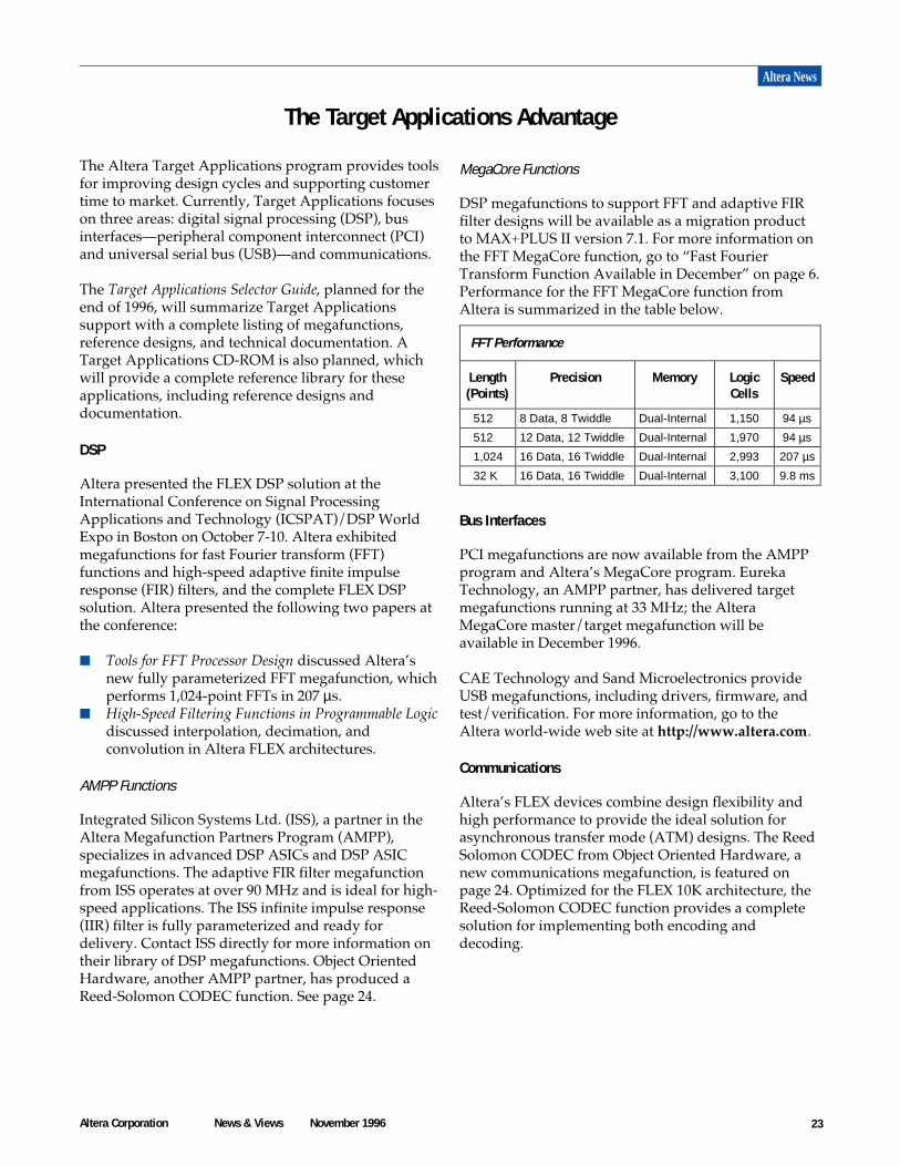
DSP megafunctions to support FFT and adaptive FIRfilter designs will be available as a migration productto MAX+PLUS II version 7.1. For more information onthe FFT MegaCore function, go to “Fast FourierTransform Function Available in December” on page 6.Performance for the FFT MegaCore function fromAltera is summarized in the table below.
Bus Interfaces
PCI megafunctions are now available from the AMPPprogram and Altera’s MegaCore program. EurekaTechnology, an AMPP partner, has delivered targetmegafunctions running at 33 MHz; the AlteraMegaCore master/target megafunction will beavailable in December 1996.
CAE Technology and Sand Microelectronics provideUSB megafunctions, including drivers, firmware, andtest/verification. For more information, go to theAltera world-wide web site at http://www.altera.com.
Communications
Altera’s FLEX devices combine design flexibility andhigh performance to provide the ideal solution forasynchronous transfer mode (ATM) designs. The ReedSolomon CODEC from Object Oriented Hardware, anew communications megafunction, is featured onpage 24. Optimized for the FLEX 10K architecture, theReed-Solomon CODEC function provides a completesolution for implementing both encoding anddecoding.
FFT Performance
Length(Points)
Precision Memory LogicCells
Speed
512 8 Data, 8 Twiddle Dual-Internal 1,150 94 µs
512 12 Data, 12 Twiddle Dual-Internal 1,970 94 µs
1,024 16 Data, 16 Twiddle Dual-Internal 2,993 207 µs
32 K 16 Data, 16 Twiddle Dual-Internal 3,100 9.8 ms

24 Altera Corporation News & Views November 1996
Altera News
Reed-Solomon CODEC Megafunction
Features
■ Foundry Independent Standard Product (FISP)■ Fully parameterized■ Corrects up to 2n erasures or n errors per block■ Continuous or burst mode operation■ Programmable generator and primitive
polynomials■ Complies with Intelsat IESS-308, Revision 6B or
RTCA DO-217 Appendix F, Revision D■ Independent encoding and decoding■ Statistics and error rate gathering options■ Fully synthesizable VHDL-RTL code■ Interface ports
– Support for serial and parallel data formats– FISPbus generic microprocessor interface
■ Applications– Satellite communications– Digital video– Magnetic and optical tape and disk drives– High performance modems– Local and wide area networks
General Description
The Reed-Solomon CODEC megafunctionprovides a complete solution for encoding anddecoding data. The megafunction alsoprovides statistical information about thenumber of correctable and uncorrectable errorsthat occur over the decoder channel. It isimplemented in VHDL and is optimized forthe Altera FLEX 10K device architecture.
Reed-Solomon Encoder
The encoder receives raw data and adds checksymbols. The codeword length and the
number of check symbols are assigned using theFISPbus interface or via direct inputs to the data block.The output produces the original data with the checksymbols appended. The delay between input andoutput depends directly on the number of checksymbols and the clocking mode. See Figure 1.
Reed-Solomon Decoder
The Reed-Solomon decoder can correct up to n symbolerrors or 2n erasures in each block of data. The receiveddata can be continuous and the delay between inputand corrected output is independent of the number oferrors or erasures. The time required to perform thecorrection depends on the codeword length and thenumber of check bits. The decoder accepts data ineither serial or parallel; the start of the block and anyerasure symbols are flagged. The decoder sequence,illustrated in Figure2, is summarized below:
■ Syndrome and error locator polynomials aregenerated.
■ Modified Euclid algorithm is performed.■ Chien search is performed.■ Statistical information is generated.
Figure 1. Reed-Solomon Encoder
Figure 2. Reed-Solomon Decoder
FISPbus
Generator PolynomialExpansion
Checksum Calculation
Control
ALTERA MEGAFUNCTION PARTNERS PROGRAM
Target Applications: Communications, Digital Signal ProcessingDevice Family: FLEX 10KVendor: Object Oriented Hardware
10-16 Tiller RoadDocklands, London E14 8PXEngland, UKTel. 44 (0) 7000 664664Fax 44 (0) 7000 664329Fax 44 (0) 171 538 2323WWW http://www.ooh.com
Statistics GatheringFISPbus
Delay
ModifiedEuclid
Algorithm
Error LocatorExpansion
SyndromeEvaluation
ErrorCollection
ChienSearch

25Altera Corporation News & Views November 1996
Reed-Solomon CODEC Parameters
Parameter Description
Number of symbols in thelongest codeblock
Expressed as two figures, (n, k), where n is the number of symbols in the codeblock after check bits areadded, and k is the original data length. The largest value of n sets the required size of the Galois field.
Symbol width Number of bits required to represent the maximum codeblock length in binary.
Required check bits anddiffering values of n and k
Each corrected error requires two check bits. For correction codes, this value is the maximum value of nand k. A small number of check bits reduces the encoder size.
Primitive polynomial Normally expressed in the form: P(x) = xm + xa + xb + xc + ... + 1
Generator polynomial The generator polynomial is shown below (where R is the number of check bits):
Number of erasures Errors at known positions. Erasures at fixed positions (i.e., end of codeblock) enable logic savings.
System clock frequency High clock frequencies reduce the latency (and hence the size of the delay line) in the decoder.
Statistic gathering functions Typically counters for errors corrected, uncorrectable codeblocks, and codeblocks received.
Serial or parallel data interfaces Internal data paths are parallel. If serial interfaces are needed, shift registers can be added.
Altera Device Selection Guide
All current information for the Altera FLEX 10K, FLEX 8000, MAX 9000, and MAX 7000 devices is listed here.Information on other Altera products is located in the Altera 1996 Data Book. Contact Altera or your local salesoffice for current product availability.
continued on page 26
In EveryI S S U E
Reed-Solomon CODEC Parameters
The following table summarizes the parameters that can be defined by the user.
G (x)
j = B
(B – 1) + R
∏ (x – αj)
10,000 10,000 20,000 20,000 30,000 30,000 40,000 40,000 50,000 50,000 50,000 70,000 70,000 100,000 100,000
Flip- flops
84-Pin PLCC, 144-Pin TQFP, 208-Pin PQFP 84-Pin PLCC, 144-Pin TQFP, 208-Pin PQFP 208-Pin RQFP, 240-Pin RQFP 208-Pin RQFP, 240-Pin RQFP 208-Pin RQFP, 240-Pin RQFP, 356-Pin BGA 208-Pin RQFP, 240-Pin RQFP, 356-Pin BGA 208-Pin RQFP, 240-Pin RQFP 208-Pin RQFP, 240-Pin RQFP 240-Pin RQFP, 356-Pin BGA, 403-Pin PGA 240-Pin RQFP, 356-Pin BGA, 403-Pin PGA 240-Pin RQFP, 356-Pin BGA, 403-Pin PGA 240-Pin RQFP, 503-Pin PGA 240-Pin RQFP, 503-Pin PGA 503-Pin PGA 503-Pin PGA
Typical Gates
Speed Grade
EPF10K10
EPF10K10 EPF10K20 EPF10K20 EPF10K30 EPF10K30 EPF10K40 EPF10K40 EPF10K50 EPF10K50 EPF10K50 EPF10K70 EPF10K70 EPF10K100 EPF10K100
-3 -4 -3 -4 -3 -4 -3 -4 -3 -4 -5 -3 -4 -3 -4
720 720
1,344 1,344 1,968 1,968 2,576 2,576 3,184 3,184 3,184 4,096 4,096 5,392 5,392
Logic Elements
FLEX 10K Devices
576 576
1,152 1,152 1,728 1,728 2,304 2,304 2,880 2,880 2,880 3,744 3,744 4,992 4,992
RAM Bits
6,144 6,144 12,288 12,288 12,288 12,288 16,384 16,384 20,480 20,480 20,480 18,432 18,432 24,576 24,576
C
C, I C
C, I C
C, I C
C, I C C
C, I C
C, I C
C, I
Temp.I/O Pins (1)Pin/Package Options
59, 102, 134 59, 102, 134
147, 189 147, 189
147, 189, 246 147, 189, 246
147, 189 147, 189
189, 274, 310 189, 274, 310 189, 274, 310
189, 358 189, 358
406 406
(1) Six I/O pins are dedicated inputs.
Device
Altera News

26 Altera Corporation News & Views November 1996
Altera Device Selection Guidecontinued from page 25
In Every Issue
2,500 2,500 2,500 2,500 4,000 4,000 4,000 6,000 6,000 6,000 8,000
8,000
8,000
12,000 12,000 12,000 16,000 16,000 16,000
84-Pin PLCC, 100-Pin TQFP 84-Pin PLCC, 100-Pin TQFP 84-Pin PLCC, 100-Pin TQFP 84-Pin PLCC, 100-Pin TQFP 84-Pin PLCC, 100-Pin TQFP, 160-Pin PGA/PQFP 84-Pin PLCC, 100-Pin TQFP, 160-Pin PGA/PQFP 84-Pin PLCC, 100-Pin TQFP, 160-Pin PGA/PQFP 84-Pin PLCC, 160-Pin PQFP, 192-Pin PGA, 208-Pin PQFP 84-Pin PLCC, 160-Pin PQFP, 192-Pin PGA, 208-Pin PQFP 84-Pin PLCC, 160-Pin PQFP, 192-Pin PGA, 208-Pin PQFP 144-Pin TQFP, 160-Pin PQFP, 192-Pin PGA, 208-Pin PQFP, 225-Pin BGA 144-Pin TQFP, 160-Pin PQFP, 192-Pin PGA, 208-Pin PQFP, 225-Pin BGA 144-Pin TQFP, 160-Pin PQFP, 192-Pin PGA, 208-Pin PQFP, 225-Pin BGA 208-Pin PQFP, 232-Pin PGA, 240-Pin PQFP 208-Pin PQFP, 232-Pin PGA, 240-Pin PQFP 208-Pin PQFP, 232-Pin PGA, 240-Pin PQFP 240-Pin PQFP, 280-Pin PGA, 304-Pin RQFP 240-Pin PQFP, 280-Pin PGA, 304-Pin RQFP 240-Pin PQFP, 280-Pin PGA, 304-Pin RQFP
Usable Gates
Pin/Package Options
EPF8282A EPF8282A EPF8282A EPF8282AV (2) EPF8452A EPF8452A EPF8452A EPF8636A EPF8636A EPF8636A EPF8820A EPF8820A EPF8820A EPF81188A EPF81188A EPF81188A EPF81500A EPF81500A EPF81500A
I/O Pins (1)
FLEX 8000 Devices
Temp. Speed Grade
A-2 A-3 A-4 A-4 A-2 A-3 A-4 A-2 A-3 A-4 A-2
A-3
A-4
A-2 A-3 A-4 A-2 A-3 A-4
C
C, I C, I C C
C, I C, I C C
C, I C C
C, I C
C, I C, I C
C, I C
208 208 208 208 336 336 336 504 504 504 672
672
672
1,008 1,008 1,008 1,296 1,296 1,296
282 282 282 282 452 452 452 636 636 636 820
820
820
1,188 1,188 1,188 1,500 1,500 1,500
Flip- flops
Logic Elements
(1) Four I/O pins are dedicated inputs. (2) V indicates 3.3-V voltage supply.
68, 78 68, 78 68, 78 68, 78 68, 120 68, 120 68, 120
68, 110, 136 68, 110, 136 68, 110, 136
120, 152
120, 152
120, 152
148, 184 148, 184 148, 184 181, 208 181, 208 181, 208
Device
-15 -20 -15 -20 -15 -20 -15 -20
C C, I C
C, I C
C, I C
C, I
60, 132, 168 60, 132, 168 59, 139, 159 59, 139, 159
146, 175 146, 175
153, 191, 216 153, 191, 216
84-Pin PLCC, 208-Pin RQFP, 280-Pin PGA 84-Pin PLCC, 208-Pin RQFP, 280-Pin PGA 84-Pin PLCC, 208-Pin RQFP, 240-Pin RQFP 84-Pin PLCC, 208-Pin RQFP, 240-Pin RQFP 208-Pin RQFP, 240-Pin RQFP 208-Pin RQFP, 240-Pin RQFP 208-Pin CQFP, 240-Pin RQFP, 280-Pin PGA, 304-Pin RQFP 208-Pin CQFP, 240-Pin RQFP, 280-Pin PGA, 304-Pin RQFP
Macrocells
Pin/Package Options
EPM9320 EPM9320 EPM9400 EPM9400 EPM9480 EPM9480 EPM9560 EPM9560
I/O Pins (1)
MAX 9000 Devices
Temp. Speed Grade
(1) Four I/O pins are dedicated inputs.
320 320 400 400 480 480 560 560
Device

27Altera Corporation News & Views November 1996
In Every Issue
178.6 150 125 100 90.9 76.9 90.9 76.9 62.5 150 125 100 90.9 76.9 150 125 100 90.9 76.9 125 100 90.9 76.9 62.5 100 76.9 125 100 90.9 76.9 62.5 125 100 90.9 76.9 62.5 125 100 90.9 76.9 62.5
-5 -6 -7 -10 -12 -15 -12 -15 -20 -6 -7 -10 -12 -15 -6 -7 -10 -12 -15 -7
-10(P) -12 -15 -20 -10 -15 -7
-10(P) -12 -15 -20 -7 -10
-12(P) -15 -20 -7 -10
-12(P) -15 -20
C C C
C, I C, I C, I C C
C, I C C
C, I C
C, I C C
C, I C
C, I C
C, I C
C, I C, I C C C
C, I C
C, I C, I C C C
C, I C, I C C C
C, I C, I
36 36 36 36 36 36 36 36 36
36, 52, 68 36, 52, 68 36, 52, 68 36, 52, 68 36, 52, 68 52, 64, 76 52, 64, 76 52, 64, 76 52, 64, 76 52, 64, 76 68, 84, 100 68, 84, 100 68, 84, 100 68, 84, 100 68, 84, 100 64, 84, 100 64, 84, 100 64, 84, 104 64, 84, 104 68, 84, 100 64, 84, 104 68, 84, 100
124 124 124 124 124
132, 164 132, 164 132, 164 132, 164 132, 164
44-Pin PLCC/TQFP 44-Pin PLCC/TQFP 44-Pin PLCC/TQFP 44-Pin PLCC/TQFP 44-Pin PLCC/TQFP 44-Pin PLCC/TQFP 44-Pin PLCC/TQFP 44-Pin PLCC/TQFP 44-Pin PLCC/TQFP 44-Pin PLCC/TQFP, 68-Pin PLCC, 84-Pin PLCC, 100-Pin PQFP 44-Pin PLCC/TQFP, 68-Pin PLCC, 84-Pin PLCC, 100-Pin PQFP 44-Pin PLCC/TQFP, 68-Pin PLCC, 84-Pin PLCC, 100-Pin PQFP 44-Pin PLCC/TQFP, 68-Pin PLCC, 84-Pin PLCC, 100-Pin PQFP 44-Pin PLCC/TQFP, 68-Pin PLCC, 84-Pin PLCC, 100-Pin PQFP 68-Pin PLCC, 84-Pin PLCC, 100-Pin PQFP 68-Pin PLCC, 84-Pin PLCC, 100-Pin PQFP 68-Pin PLCC, 84-Pin PLCC, 100-Pin PQFP 68-Pin PLCC, 64-Pin PLCC, 100-Pin PQFP 68-Pin PLCC, 84-Pin PLCC, 100-Pin PQFP 84-Pin PLCC, 100-Pin PQFP, 160-Pin PQFP 84-Pin PLCC, 100-Pin PQFP, 160-Pin PQFP 84-Pin PLCC, 100-Pin PQFP, 160-Pin PQFP 84-Pin PLCC, 100-Pin PQFP, 160-Pin PQFP 84-Pin PLCC, 100-Pin PQFP, 160-Pin PQFP 84-Pin PLCC, 100-Pin PQFP, 160-Pin PQFP 84-Pin PLCC, 100-Pin PQFP, 160-Pin PQFP 84-Pin PLCC, 100-Pin PQFP, 160-Pin PQFP 84-Pin PLCC, 100-Pin PQFP, 160-Pin PQFP 84-Pin PLCC, 100-Pin PQFP, 160-Pin PQFP 84-Pin PLCC, 100-Pin PQFP, 160-Pin PQFP 84-Pin PLCC, 100-Pin PQFP, 160-Pin PQFP 160-Pin PQFP/PGA 160-Pin PQFP/PGA 160-Pin PQFP/PGA 160-Pin PQFP/PGA 160-Pin PQFP/PGA 160-Pin PQFP, 192-Pin PGA, 208-Pin RQFP 160-Pin PQFP, 192-Pin PGA, 208-Pin RQFP 160-Pin PQFP, 192-Pin PGA, 208-Pin RQFP 160-Pin PQFP, 192-Pin PGA, 208-Pin RQFP 160-Pin PQFP, 192-Pin PGA, 208-Pin RQFP
32 32 32 32 32 32 32 32 32 64 64 64 64 64 96 96 96 96 96 128 128 128 128 128 128 128 160 160 160 160 160 192 192 192 192 192 256 256 256 256 256
Macrocells
Pin/Package Options
EPM7032, EPM7032S EPM7032, EPM7032S EPM7032, EPM7032S EPM7032, EPM7032S EPM7032 EPM7032, EPM7032S EPM7032V (2) EPM7032V (2) EPM7032V (2) EPM7064, EPM7064S EPM7064, EPM7064S EPM7064, EPM7064S EPM7064 EPM7064, EPM7064S EPM7096, EPM7096S EPM7096, EPM7096S EPM7096, EPM7096S EPM7096 EPM7096, EPM7096S EPM7128E, EPM7128S EPM7128E, EPM7128S EPM7128E EPM7128E, EPM7128S EPM7128E EPM7128SV (2) EPM7128SV (2 ) EPM7160E, EPM7160S EPM7160E, EPM7160S EPM7160E EPM7160E, EPM7160S EPM7160E EPM7192E, EPM7192S EPM7192E, EPM7192S EPM7192E EPM7192E, EPM7192S EPM7192E EPM7256E, EPM7256S EPM7256E, EPM7256S EPM7256E EPM7256E, EPM7256S EPM7256E
I/O Pins (1)
MAX 7000 Devices
Temp. Speed Grade
tPD (ns)
fCNT (MHz)
(1) Four I/O pins are dedicated inputs. (2) V indicates 3.3-V voltage supply.
5 6
7.5 10 12 15 12 15 20 6
7.5 10 12 15 6
7.5 10 12 15 7.5 10 12 15 20 10 15 7.5 10 12 15 20 7.5 10 12 15 20 7.5 10 12 15 20
Device

28 Altera Corporation News & Views November 1996
eau000.exe Overview of electronic utilitieseau003.exe EP310 to EP330 JEDEC File convertereau005.exe JEDPACK JEDEC File compactoreau007.exe JEDSUM JEDEC checksum generatoreau017.exe LEF2AHDL converts A+PLUS LEF files
to AHDLeau018.exe PLD2EQN PAL/GAL/PLA file
converter
Data I/O provides programming hardware support forselect Altera devices. Algorithms are supplied viaData I/O’s Keep Current Express - Bulletin BoardService (KCE-BBS). Programming support forConfiguration EPROM, MAX 9000, MAX 7000, andFLASHlogic devices is shown below. All information issubject to change. Data I/O customers with a currentmaintenance agreement can obtain qualifiedalgorithms electronically from the KCE-BBS.
The following Configuration EPROM devices aresupported by the 2900 version 5.3, the 3900 version 5.3,and UniSite version 5.3 (Hex Files only).
■ EPC1213P-8■ EPC1213L-20■ EPC1064P-8■ EPC1064L-20■ EPC1064T-20■ EPC1064VL■ EPC1064VT■ EPC1P-8■ EPC1LC-20
The following MAX 9000, MAX 7000, and FLASHlogicdevices are supported by the 3900 version 5.3 andUniSite version 5.3.
MAX 9000 Devices
■ EPM9320LC84■ EPM9320GC280■ EPM9320RC208■ EPM9400RC208■ EPM9400RC240■ EPM9480RC208■ EPM9480RC240■ EPM9560GC280■ EPM9560RC240■ EPM9560WC208■ EPM9560RC304
Data I/O Programming SupportMAX 7000 Devices
■ EPM7032L-44■ EPM7032Q-44■ EPM7032T-44■ EPM7032VL-44■ EPM7032VT-44■ EPM7064L-44■ EPM7064L-68■ EPM7064L-84■ EPM7064Q-100■ EPM7096L-68 (EPROM)■ EPM7096L-84 (EPROM)■ EPM7096Q-100 (EPROM)■ EPM7096L-68 (EEPROM)■ EPM7096L-84 (EEPROM)■ EPM7096Q-100 (EEPROM)■ EPM7128L-84■ EPM7128Q-100■ EPM7128Q-160■ EPM7128EL-84■ EPM7128EQ-100■ EPM7128EQ-160■ EPM7160L-84■ EPM7160Q-160■ EPM7160EL-84■ EPM7160EQ-100■ EPM7160EQ-160■ EPM7192G-160■ EPM7192Q-160■ EPM7192EG-160■ EPM7192EQ-160■ EPM7256G-192■ EPM7256W-208■ EPM7256M-208■ EPM7256EG-192■ EPM7256EG-160■ EPM7256ER-208
FLASHlogic Devices
■ EPX880
In Every Issue
eau019.exe ABEL2MAX file convertereau020.exe PASM2TDF PALASM file convertereau022.exe PLA2PDS PLA to PALASM file
converter
Utilities are available from the Altera BBS viamodem at (408) 954-0104 and the Altera FTP site atftp.altera.com.
Software Utilities

29Altera Corporation News & Views November 1996
Programming Hardware CompatibilityThe following tables contain the latestprogramming hardware information. Toensure correct programming, you shouldalways use the software version shown in“Current Software Versions” below. PLM-prefix adapters can be used only with theMaster Programming Unit (MPU).
Notes to tables:(1) MAX+PLUS II version 7.0 and higher provides programming support for
all FLASHlogic devices via the BitBlaster and ByteBlaster.(2) You can use the FLASHlogic Download Cable (PL-FLDLC) with PLDshell
Plus to program and configure all FLASHlogic devices.(3) The hardware products for these devices are included with the FLEX
Download Cable.(4) Refer to the Altera 1996 Data Book for device adapter information. Altera
offers an adapter exchange program for 0.8-micron EPM5032, EPM5064,and EPM5130 programming adapters. See “Product Transitions” on page 5of this newsletter for more information.
In Every Issue
Programming Adapters
Device Package Adapter
EPC1064, EPC1064V, EPC1213
(all FLEX 8000 devices), Note (3)DIP, J-lead
TQFP
PLMJ1213
PLMT1064
EPC1 (all FLEX 10K and
FLEX 8000 devices), Note (3)DIP
J-lead
PLMJ1213 PLMJ1213
EPM9320 PGA
J-lead (84-pin)
RQFP (208-pin)
PLMG9000-280
PLMJ9320-84
PLMR9000-208
EPM9400 J-lead (84-pin)
RQFP (208-pin)
RQFP (240-pin)
PLMJ9400-84
PLMR9000-208
PLMR9000-240
EPM9480 RQFP (208-pin)
RQFP (240-pin)
PLMR9000-208
PLMR9000-240
EPM9560 PGA
RQFP (208-pin)
RQFP (240-pin)
RQFP (304-pin)
PLMG9000-280
PLMR9000-208
PLMR9000-240
PLMR9000-304
EPM7032, EPM7032V J-lead
PQFP
TQFP
PLMJ7000-44
PLMQ7000-44
PLMT7000-44
EPM7064 J-lead (68-pin)
J-lead (84-pin)
PQFP
PLMJ7000-68
PLMJ7000-84 PLMQ7000-100
EPM7096 J-lead (68-pin)
J-lead (84-pin)
PQFP
PLMJ7000-68
PLMJ7000-84 PLMQ7000-100
EPM7128, EPM7128E J-lead (84-pin)
PQFP (100-pin)
PQFP (160-pin)
PLMJ7000-84
PLMQ7000-100
PLMQ7128/7160-160
EPM7160, EPM7160E J-lead
PQFP (100-pin)
PQFP (160-pin)
PLMJ7000-84
PLMQ7000-100
PLMQ7128/7160-160
EPM7192, EPM7192E PGA
PQFP
PLMG7192-160
PLMQ7192/7256-160
EPM7256E PGA
MQFP, RQFP
PQFP
PLMG7256-192 PLMR7256-208
PLMQ7192/7256-160
EPX780 J-lead PLMJ780-84
MAX 5000 devices All packages Note (4)
Classic devices All packages Note (4)
EPS448 All packages Note (4)
Current Software Versions
The latest versions of Altera softwareproducts are shown below:
■ MAX+PLUS II version 7.1, availableDecember 1996(PC, Sun SPARCstation, HP 9000Series 700, and IBMRISC System/6000 platforms)
■ PLDshell Plus version 5.1 (PC only)
Programming with the BitBlaster & ByteBlaster
Device Package Hardware
FLEX 10K All packages PL-BITBLASTER
PL-BYTEBLASTER
FLEX 8000 All packages PL-BITBLASTER
PL-BYTEBLASTER
MAX 9000 All packages PL-BITBLASTER
PL-BYTEBLASTER
MAX 7000S All packages PL-BITBLASTER
PL-BYTEBLASTER
EPX880 All packages PL-BITBLASTER
PL-BYTEBLASTER,
Note (1)
FLASHlogic All packages PL-FLDLC,
PL-BITBLASTER,
PL-BYTEBLASTER
Notes (1), (2)
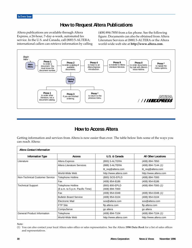
30 Altera Corporation News & Views November 1996
How to Request Altera PublicationsAltera publications are available through AlteraExpress, a 24-hour, 7-day-a-week, automated faxservice. In the U.S. and Canada, call (800) 5-ALTERA;international callers can retrieve information by calling
(408) 894-7850 from a fax phone. See the followingfigure. Documents can also be obtained from AlteraLiterature Services at (888) 3-ALTERA or the Alteraworld-wide web site at http://www.altera.com.
How to Access Altera
Getting information and services from Altera is now easier than ever. The table below lists some of the ways youcan reach Altera:
Note:(1) You can also contact your local Altera sales office or sales representative. See the Altera 1996 Data Book for a list of sales offices
and representatives.
CatalogMenu
Press 1to order other
literature, not adocument catalog.
Press 3if you are finished
ordering.
Press *to return to theprevious menu.
Press 1to order a
document. Youmust know the
document number.
Press 2to order a catalog of
availabledocuments.
Press 4to listen to anAltera Expressintroduction.
Press 9to transfer to AlteraLiterature Services.
Press 0to order documentsby mail with Altera’s
Voice Hotline.
Press *to repeat the
menu options.
MainMenu
BeginHere
In Every Issue
Altera Contact Information
Information Type Access U.S. & Canada All Other Locations
Literature Altera Express (800) 5-ALTERA (408) 894-7850
Altera Literature Services (888) 3-ALTERA
(408) 894-7144 (1)
World-Wide Web http://www.altera.com http://www.altera.com
Non-Technical Customer Service Telephone Hotline (800) SOS-EPLD (408) 894-7000
Fax (408) 954-8186 (408) 954-8186
Technical Support Telephone Hotline(8 a.m. to 5 p.m. Pacific Time)
(800) 800-EPLD (408) 894-7000
(408) 894-7000 (1)
Fax (408) 954-0348 (408) 954-0348 (1)
Bulletin Board Service (408) 954-0104 (408) 954-0104
Electronic Mail [email protected] [email protected]
FTP Site ftp.altera.com ftp.altera.com
CompuServe go altera go altera
General Product Information Telephone (408) 894-7104 (408) 894-7104 (1)
World-Wide Web http://www.altera.com http://www.altera.com

31Altera Corporation News & Views November 1996
Please fax or mail a copy of this page to:Altera Literature Distribution ServicesAltera Corporation2610 Orchard ParkwaySan Jose, CA 95134-2020Fax: (408) 894-7809E-mail: [email protected]
Fax Response Form
Please write your comments about News & Views in the space below (use additional pages if necessary). Whichsubjects are not getting enough coverage? What questions do you still have? What new features would you like tosee?
I would like a subscription toNews & Views.
I would like to have my designfeatured in News & Views.
Please correct my address.
Your Name:
Organization:
Street Address:
City, State, ZIP:
Phone:
E-Mail:
Tell Us What You ThinkPlease take a moment to help us improve News & Views by rating the usefulness of the following sections. Youranswers will help shape the content of future issues.
Not VeryUseful Useful
1. Devices & Tools 1 2 3 4 52. New Altera Publications 1 2 3 4 53. Questions & Answers 1 2 3 4 54. Technical “How To” Articles 1 2 3 4 55. Information on Altera’s 1 2 3 4 5
EDA Partners & Interface Support 1 2 3 4 56. Customer Applications 1 2 3 4 57. Software Utilities & Current
Software versions 1 2 3 4 58. Altera News 1 2 3 4 5
®