amd geode™ gx and lx processor based systems … · the system manager manages descriptors for...
TRANSCRIPT
AMD Geode™ GX and LX Processor Based SystemsVirtualized PCI Configuration Space
November 2006Publication ID: 32663C
AMD Geode™ GX and LX Processor Based Systems Virtualized PCI Configuration Space

2 AMD Geode™ GX and LX Processor Based Systems Virtualized PCI Configuration Space
© 2006 Advanced Micro Devices, Inc. All rights reserved.The contents of this document are provided in connection with Advanced MicroDevices, Inc. (“AMD”) products. AMD makes no representations or warranties withrespect to the accuracy or completeness of the contents of this publication andreserves the right to make changes to specifications and product descriptions atany time without notice. No license, whether express, implied, arising by estoppelor otherwise, to any intellectual property rights is granted by this publication.Except as set forth in AMD’s Standard Terms and Conditions of Sale, AMDassumes no liability whatsoever, and disclaims any express or implied warranty,relating to its products including, but not limited to, the implied warranty of mer-chantability, fitness for a particular purpose, or infringement of any intellectualproperty right.
AMD’s products are not designed, intended, authorized or warranted for use ascomponents in systems intended for surgical implant into the body, or in otherapplications intended to support or sustain life, or in any other application in whichthe failure of AMD’s product could create a situation where personal injury, death,or severe property or environmental damage may occur. AMD reserves the right todiscontinue or make changes to its products at any time without notice.
Trademarks
AMD, the AMD Arrow logo, Geode, and combinations thereof, and GeodeLink are trademarks of Advanced Micro Devices, Inc.
Other product names used in this publication are for identification purposes only and may be trademarks of their respective companies.
Contents 32663C
Contents
List of Figures . . . . . . . . . . . . . . . . . . . . . . . . . . . . . . . . . . . . . . . . . . . . . . . . . . . . . . . . . . 5
List of Tables . . . . . . . . . . . . . . . . . . . . . . . . . . . . . . . . . . . . . . . . . . . . . . . . . . . . . . . . . . . 7
1.0 Overview . . . . . . . . . . . . . . . . . . . . . . . . . . . . . . . . . . . . . . . . . . . . . . . . . . . . . . . . . . 91.1 Scope . . . . . . . . . . . . . . . . . . . . . . . . . . . . . . . . . . . . . . . . . . . . . . . . . . . . . . . . . . . . . . . . . . . . . . 91.2 Background . . . . . . . . . . . . . . . . . . . . . . . . . . . . . . . . . . . . . . . . . . . . . . . . . . . . . . . . . . . . . . . . . 9
2.0 Implementation . . . . . . . . . . . . . . . . . . . . . . . . . . . . . . . . . . . . . . . . . . . . . . . . . . . 112.1 VSA Initialization . . . . . . . . . . . . . . . . . . . . . . . . . . . . . . . . . . . . . . . . . . . . . . . . . . . . . . . . . . . . 112.2 Virtualized PCI Topology . . . . . . . . . . . . . . . . . . . . . . . . . . . . . . . . . . . . . . . . . . . . . . . . . . . . . . 152.3 Synchronization . . . . . . . . . . . . . . . . . . . . . . . . . . . . . . . . . . . . . . . . . . . . . . . . . . . . . . . . . . . . . 162.4 Embedded PCI Devices (CS5535 Only) . . . . . . . . . . . . . . . . . . . . . . . . . . . . . . . . . . . . . . . . . . 16
3.0 PCI Header . . . . . . . . . . . . . . . . . . . . . . . . . . . . . . . . . . . . . . . . . . . . . . . . . . . . . . . 173.1 Vendor ID . . . . . . . . . . . . . . . . . . . . . . . . . . . . . . . . . . . . . . . . . . . . . . . . . . . . . . . . . . . . . . . . . . 183.2 Device ID . . . . . . . . . . . . . . . . . . . . . . . . . . . . . . . . . . . . . . . . . . . . . . . . . . . . . . . . . . . . . . . . . . 183.3 Command Register . . . . . . . . . . . . . . . . . . . . . . . . . . . . . . . . . . . . . . . . . . . . . . . . . . . . . . . . . . 183.4 Status Register . . . . . . . . . . . . . . . . . . . . . . . . . . . . . . . . . . . . . . . . . . . . . . . . . . . . . . . . . . . . . 203.5 Revision ID . . . . . . . . . . . . . . . . . . . . . . . . . . . . . . . . . . . . . . . . . . . . . . . . . . . . . . . . . . . . . . . . . 213.6 Class Code . . . . . . . . . . . . . . . . . . . . . . . . . . . . . . . . . . . . . . . . . . . . . . . . . . . . . . . . . . . . . . . . 213.7 Cache Line Size . . . . . . . . . . . . . . . . . . . . . . . . . . . . . . . . . . . . . . . . . . . . . . . . . . . . . . . . . . . . . 213.8 Latency Timer . . . . . . . . . . . . . . . . . . . . . . . . . . . . . . . . . . . . . . . . . . . . . . . . . . . . . . . . . . . . . . 213.9 Header Type . . . . . . . . . . . . . . . . . . . . . . . . . . . . . . . . . . . . . . . . . . . . . . . . . . . . . . . . . . . . . . . 213.10 BIST . . . . . . . . . . . . . . . . . . . . . . . . . . . . . . . . . . . . . . . . . . . . . . . . . . . . . . . . . . . . . . . . . . . . . . 213.11 Base Address Registers . . . . . . . . . . . . . . . . . . . . . . . . . . . . . . . . . . . . . . . . . . . . . . . . . . . . . . 223.12 Subsystem Vendor ID . . . . . . . . . . . . . . . . . . . . . . . . . . . . . . . . . . . . . . . . . . . . . . . . . . . . . . . . 233.13 Subsystem ID . . . . . . . . . . . . . . . . . . . . . . . . . . . . . . . . . . . . . . . . . . . . . . . . . . . . . . . . . . . . . . 233.14 Capabilities Pointer . . . . . . . . . . . . . . . . . . . . . . . . . . . . . . . . . . . . . . . . . . . . . . . . . . . . . . . . . . 233.15 Interrupt Line . . . . . . . . . . . . . . . . . . . . . . . . . . . . . . . . . . . . . . . . . . . . . . . . . . . . . . . . . . . . . . . 233.16 Interrupt Pin . . . . . . . . . . . . . . . . . . . . . . . . . . . . . . . . . . . . . . . . . . . . . . . . . . . . . . . . . . . . . . . . 233.17 Min_Gnt Register . . . . . . . . . . . . . . . . . . . . . . . . . . . . . . . . . . . . . . . . . . . . . . . . . . . . . . . . . . . . 233.18 Max_Lat Register . . . . . . . . . . . . . . . . . . . . . . . . . . . . . . . . . . . . . . . . . . . . . . . . . . . . . . . . . . . . 233.19 OEM Registers . . . . . . . . . . . . . . . . . . . . . . . . . . . . . . . . . . . . . . . . . . . . . . . . . . . . . . . . . . . . . 23
4.0 PCI Interrupts . . . . . . . . . . . . . . . . . . . . . . . . . . . . . . . . . . . . . . . . . . . . . . . . . . . . . 254.1 PCI Interrupt Steering . . . . . . . . . . . . . . . . . . . . . . . . . . . . . . . . . . . . . . . . . . . . . . . . . . . . . . . . 25
AMD Geode™ GX and LX Processor Based Systems Virtualized PCI Configuration Space 3

Contents32663C
5.0 VSM Support . . . . . . . . . . . . . . . . . . . . . . . . . . . . . . . . . . . . . . . . . . . . . . . . . . . . . 275.1 SYS_LOOKUP_DEVICE . . . . . . . . . . . . . . . . . . . . . . . . . . . . . . . . . . . . . . . . . . . . . . . . . . . . . . 275.2 SYS_ALLOCATE_RESOURCE . . . . . . . . . . . . . . . . . . . . . . . . . . . . . . . . . . . . . . . . . . . . . . . . . 285.3 SYS_GET_DESCRIPTOR . . . . . . . . . . . . . . . . . . . . . . . . . . . . . . . . . . . . . . . . . . . . . . . . . . . . . 295.4 GET_DESCR_INFO . . . . . . . . . . . . . . . . . . . . . . . . . . . . . . . . . . . . . . . . . . . . . . . . . . . . . . . . . 295.5 SYS_MAP_IRQ . . . . . . . . . . . . . . . . . . . . . . . . . . . . . . . . . . . . . . . . . . . . . . . . . . . . . . . . . . . . . 29
Appendix A Support Documentation . . . . . . . . . . . . . . . . . . . . . . . . . . . . . . . . . . . . . 31A.1 AMD Geode™ GX Processor/CS5535 Companion Device MSR Address Values . . . . . . . . . . 31A.2 AMD Geode™ LX Processor/CS5536 Companion Device MSR Address Values . . . . . . . . . . 39A.3 Revision History . . . . . . . . . . . . . . . . . . . . . . . . . . . . . . . . . . . . . . . . . . . . . . . . . . . . . . . . . . . . 50
4 AMD Geode™ GX and LX Processor Based Systems Virtualized PCI Configuration Space
List of Figures 32663C
List of Figures
Figure 3-1. Standard Type 0 PCI Header Format . . . . . . . . . . . . . . . . . . . . . . . . . . . . . . . . . . . . . . . . . . 17
AMD Geode™ GX and LX Processor Based Systems Virtualized PCI Configuration Space 5

List of Figures32663C
6 AMD Geode™ GX and LX Processor Based Systems Virtualized PCI Configuration Space
List of Tables 32663C
List of Tables
Table 2-1. GLPCI MSR Initialization . . . . . . . . . . . . . . . . . . . . . . . . . . . . . . . . . . . . . . . . . . . . . . . . . . . . 11Table 2-2. GLIU0 Descriptors . . . . . . . . . . . . . . . . . . . . . . . . . . . . . . . . . . . . . . . . . . . . . . . . . . . . . . . . . 12Table 2-3. GLIU1 Descriptors . . . . . . . . . . . . . . . . . . . . . . . . . . . . . . . . . . . . . . . . . . . . . . . . . . . . . . . . . 13Table 2-4. Companion Device GLIU Descriptors . . . . . . . . . . . . . . . . . . . . . . . . . . . . . . . . . . . . . . . . . . 14Table 2-5. AMD Geode™ GX Processor Header Layout . . . . . . . . . . . . . . . . . . . . . . . . . . . . . . . . . . . . 15Table 2-6. AMD Geode™ LX Processor Header Layout . . . . . . . . . . . . . . . . . . . . . . . . . . . . . . . . . . . . 15Table 2-7. Virtualized AMD Geode™ CS5535 Companion Device Header . . . . . . . . . . . . . . . . . . . . . . 15Table 2-8. Virtualized AMD Geode™ CS5536 Companion Device Header . . . . . . . . . . . . . . . . . . . . . . 16Table 3-1. Status Register . . . . . . . . . . . . . . . . . . . . . . . . . . . . . . . . . . . . . . . . . . . . . . . . . . . . . . . . . . . 20Table 3-2. Revision ID Values . . . . . . . . . . . . . . . . . . . . . . . . . . . . . . . . . . . . . . . . . . . . . . . . . . . . . . . . . 21Table 3-3. BAR Usage Per Function . . . . . . . . . . . . . . . . . . . . . . . . . . . . . . . . . . . . . . . . . . . . . . . . . . . . 22Table A-1. Standard PCI Header for F0 - ISA Bridge . . . . . . . . . . . . . . . . . . . . . . . . . . . . . . . . . . . . . . . 33Table A-2. Standard PCI Header for F1 - Flash Controller . . . . . . . . . . . . . . . . . . . . . . . . . . . . . . . . . . . 34Table A-3. Standard PCI Header for F2 - IDE Controller . . . . . . . . . . . . . . . . . . . . . . . . . . . . . . . . . . . . 35Table A-4. Standard PCI Header for F3 - Audio Device . . . . . . . . . . . . . . . . . . . . . . . . . . . . . . . . . . . . . 36Table A-5. Standard PCI Header for F4 - USB Controller #1 . . . . . . . . . . . . . . . . . . . . . . . . . . . . . . . . . 37Table A-6. Standard PCI Header for F5 - USB Controller #2 . . . . . . . . . . . . . . . . . . . . . . . . . . . . . . . . . 38Table A-7. Standard PCI Header for F0 - ISA Bridge . . . . . . . . . . . . . . . . . . . . . . . . . . . . . . . . . . . . . . . 42Table A-8. Standard PCI Header for F1 - Flash Controller . . . . . . . . . . . . . . . . . . . . . . . . . . . . . . . . . . . 43Table A-9. Standard PCI Header for F2 - IDE Controller . . . . . . . . . . . . . . . . . . . . . . . . . . . . . . . . . . . . 44Table A-10. Standard PCI Header for F3 - Audio Device . . . . . . . . . . . . . . . . . . . . . . . . . . . . . . . . . . . . . 45Table A-11. Standard PCI Header for F4 - USB OHCI Controller . . . . . . . . . . . . . . . . . . . . . . . . . . . . . . . 46Table A-12. Standard PCI Header for F5 - USB EHCI Controller . . . . . . . . . . . . . . . . . . . . . . . . . . . . . . . 47Table A-13. Standard PCI Header for F6 - USB UDC Controller . . . . . . . . . . . . . . . . . . . . . . . . . . . . . . . 48Table A-14. Standard PCI Header for F7 - USB OTG Controller . . . . . . . . . . . . . . . . . . . . . . . . . . . . . . . 49Table A-15. Revision History . . . . . . . . . . . . . . . . . . . . . . . . . . . . . . . . . . . . . . . . . . . . . . . . . . . . . . . . . . . 50
AMD Geode™ GX and LX Processor Based Systems Virtualized PCI Configuration Space 7

List of Tables32663C
8 AMD Geode™ GX and LX Processor Based Systems Virtualized PCI Configuration Space

AMD Geode™ GX and LX Processo
Overview 32663C
11.0Overview
1.1 ScopeThis document discusses the issues related to the virtualization of PCI configuration headers on systems based on theAMD Geode™ GX and LX processors, and the AMD Geode™ CS5535 and CS5536 companion devices (hereafter referredto as AMD Geode processor and AMD Geode companion device).
1.2 BackgroundAMD Geode processor-based systems support the industry standard enumeration of PCI devices. However, the AMDGeodeLink™ architecture has centralized address decoding while the PCI bus has decentralized address decoding. Fur-thermore, the AMD Geode processor and companion device do not implement complete PCI bus controllers. To resolve thisdiscrepancy, GeodeLink devices that must be identified and configured by an operating system have their PCI configurationspaces virtualized by AMD Virtual System Architecture (VSA) technology.
r Based Systems Virtualized PCI Configuration Space 9

Background32663C
10 AMD Geode™ GX and LX Processor Based Systems Virtualized PCI Configuration Space

Implementation 32663C
22.0Implementation
The GeodeLink PCI (GLPCI) module in the AMD Geode processor implements the standard CF8h/CFCh mechanism toaccess PCI configuration space. The default setting is for all PCI configuration cycles to be sent to the external PCI bus.The GLPCI module may be configured to generate a Synchronous System Management Interrupt (SSMI) on configurationcycles to selected devices, as determined by the Device Number field of the PCI configuration address. All other PCI con-figuration cycles (e.g., external PCI devices) are subtractively routed to the PCI bus. VSA responds to SSMIs from theGLPCI by emulating accesses to the referenced PCI configuration space. For example, when a read of a configuration reg-ister occurs, VSA returns, in the caller’s AL/AX/EAX register, the correct value from internal VSA tables representing thestate of the PCI header. Reads of some PCI registers require GeodeLink Model Specific Registers (MSRs) to be read inorder to determine the appropriate value. This process is discussed in general terms in Section 2.3 "Synchronization" onpage 16 and in detail in Section 3.0 "PCI Header" on page 17.
Writes, to read only fields, are sent to the bit-bucket. Most of the virtualization functionality lies in implementing the Status,Command and Base Address registers. Reading unused registers returns zeros, and writes to unused registers areignored. Reading unimplemented functions returns FFh, and writes to unimplemented functions are ignored.
Unaligned accesses are supported. For example, a DWORD read of a non-DWORD aligned PCI address returns FFh inthe bytes that are not part of the addressed DWORD. Similarly, a DWORD write of a non-DWORD aligned PCI addresswrites only the bytes contained in the addressed DWORD. The remaining data is discarded. Wrapping to the following reg-ister does not occur, just as in hardware PCI headers.
VSA technology supports trapping of I/O accesses. In AMD Geode processor-based systems, the GeodeLink Interface Unit(GLIU) descriptors are used to generate an SSMI on a descriptor hit.
2.1 VSA Initialization
2.1.1 MSRs InitializationVSA initializes certain MSRs in order to implement PCI virtualization.
2.1.1.1 GLPCIThe address of the AMD Geode processor’s GLPCI module is 2.4.0.0.0.0. MSRs within the GLPCI module are initialized asshown in Table 2-1.
Table 2-1. GLPCI MSR Initialization
MSR Field Description MSR Address
CTRL[0] Set to 1 to enable in-bound memory transactions from the PCI bus. 2010h
PBUS Set to 00008002h. 2012h
ExtMSR Should be set by the BIOS as follows:
Set to 00000000h_00000F00h to route MSR mailbox transactions to PCI device number 15 (IDSEL 25). This yields MSR addresses in the companion device of 2.4.2.x.x.x
201Eh
AMD Geode™ GX and LX Processor Based Systems Virtualized PCI Configuration Space 11
Implementation32663C
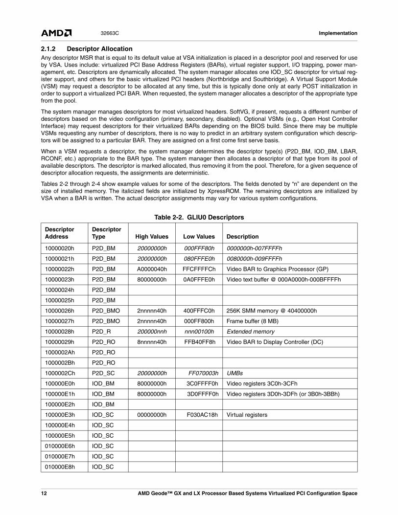
2.1.2 Descriptor AllocationAny descriptor MSR that is equal to its default value at VSA initialization is placed in a descriptor pool and reserved for useby VSA. Uses include: virtualized PCI Base Address Registers (BARs), virtual register support, I/O trapping, power man-agement, etc. Descriptors are dynamically allocated. The system manager allocates one IOD_SC descriptor for virtual reg-ister support, and others for the basic virtualized PCI headers (Northbridge and Southbridge). A Virtual Support Module(VSM) may request a descriptor to be allocated at any time, but this is typically done only at early POST initialization inorder to support a virtualized PCI BAR. When requested, the system manager allocates a descriptor of the appropriate typefrom the pool.
The system manager manages descriptors for most virtualized headers. SoftVG, if present, requests a different number ofdescriptors based on the video configuration (primary, secondary, disabled). Optional VSMs (e.g., Open Host ControllerInterface) may request descriptors for their virtualized BARs depending on the BIOS build. Since there may be multipleVSMs requesting any number of descriptors, there is no way to predict in an arbitrary system configuration which descrip-tors will be assigned to a particular BAR. They are assigned on a first come first serve basis.
When a VSM requests a descriptor, the system manager determines the descriptor type(s) (P2D_BM, IOD_BM, LBAR,RCONF, etc.) appropriate to the BAR type. The system manager then allocates a descriptor of that type from its pool ofavailable descriptors. The descriptor is marked allocated, thus removing it from the pool. Therefore, for a given sequence ofdescriptor allocation requests, the assignments are deterministic.
Tables 2-2 through 2-4 show example values for some of the descriptors. The fields denoted by “n” are dependent on thesize of installed memory. The italicized fields are initialized by XpressROM. The remaining descriptors are initialized byVSA when a BAR is written. The actual descriptor assignments may vary for various system configurations.
Table 2-2. GLIU0 Descriptors
Descriptor Address
DescriptorType High Values Low Values Description
10000020h P2D_BM 20000000h 000FFF80h 0000000h-007FFFFh
10000021h P2D_BM 20000000h 080FFFE0h 0080000h-009FFFFh
10000022h P2D_BM A0000040h FFCFFFFCh Video BAR to Graphics Processor (GP)
10000023h P2D_BM 80000000h 0A0FFFE0h Video text buffer @ 000A0000h-000BFFFFh
10000024h P2D_BM
10000025h P2D_BM
10000026h P2D_BMO 2nnnnn40h 400FFFC0h 256K SMM memory @ 40400000h
10000027h P2D_BMO 2nnnnn40h 000FF800h Frame buffer (8 MB)
10000028h P2D_R 200000nnh nnn00100h Extended memory
10000029h P2D_RO 8nnnnn40h FFB40FF8h Video BAR to Display Controller (DC)
1000002Ah P2D_RO
1000002Bh P2D_RO
1000002Ch P2D_SC 20000000h FF070003h UMBs
100000E0h IOD_BM 80000000h 3C0FFFF0h Video registers 3C0h-3CFh
100000E1h IOD_BM 80000000h 3D0FFFF0h Video registers 3D0h-3DFh (or 3B0h-3BBh)
100000E2h IOD_BM
100000E3h IOD_SC 00000000h F030AC18h Virtual registers
100000E4h IOD_SC
100000E5h IOD_SC
010000E6h IOD_SC
010000E7h IOD_SC
010000E8h IOD_SC
12 AMD Geode™ GX and LX Processor Based Systems Virtualized PCI Configuration Space

Implementation 32663C
Table 2-3. GLIU1 Descriptors
Descriptor Address
DescriptorType High Values Low Values Description
40000020h P2D_BM 20000000h 000FFF80 0000000h-007FFFFh
40000021h P2D_BM 20000000h 080FFFE0 0080000h-009FFFFh
40000022h P2D_BM 20000040h FFCFFFFC GP video BAR to GLIU0
40000023h P2D_BM 20000040h 400FFFC0h 256K SMM memory to GLIU0
40000024h P2D_BM 20000040h FF8FFFFCh DC video BAR to GLIU0
40000025h P2D_BM 40000040h FF4FFFFCh VP video BAR
40000026h P2D_BM 20000000h 0A0FFFC0h Video text buffer to GLIU0
40000027h P2D_BM A0000040h FF0FFFFCh Video BAR to VIP
40000028h P2D_BM
40000029h P2D_R 200000nnh nnn00100h Extended memory
4000002Ah P2D_R 20000041h 7FF41000h Frame buffer (8 MB)
4000002Bh P2D_R C00000EFh FFBEFFF8h AES BAR
4000002Ch P2D_R
4000002Dh P2D_SC 20000000h FF070003h UMBs
400000E0h IOD_BM 20000000h 3C0FFFF0h Video registers 3C0h-3CFh to GLIU0
400000E1h IOD_BM 20000000h 3D0FFFF0h Video registers 3D0h-3DFh to GLIU0
400000E2h IOD_BM
400000E3h IOD_SC 60000000h 033000F0h I/O F0h-F1h to GIO logic in GLCP
400000E4h IOD_SC
400000E5h IOD_SC
400000E6h IOD_SC
400000E7h IOD_SC
400000E8h IOD_SC
AMD Geode™ GX and LX Processor Based Systems Virtualized PCI Configuration Space 13

Implementation32663C
Table 2-4. Companion Device GLIU Descriptors
Descriptor Address
DescriptorType High Values Low Values Description
51010020h P2D_BM
51010021h P2D_BM
51010022h P2D_BM
51010023h P2D_BMK See Section A.2.4 on page 42 Routes the Open Host Controller Interface (OHCI) Legacy support registers to KEL
51010024h P2D_BMK See Section A.2.4 on page 42 Routes the Enhanced Host Control-ler Interface (EHCI) registers
51010025h P2D_BM See Section A.2.4 on page 42 Routes the Universal Device Con-troller (UDC) registers
51010026h P2D_BM See Section A.2.4 on page 42 Routes the On-The-Go (OTG) reg-isters
510100E0h IOD_BM 60000000h 1F0FFFF8h Routes the ATA registers
510100E1h IOD_BM See Section A.2.4 on page 42 Routes the AC97 registers
510100E2h IOD_BM
510100E3h IOD_BM
510100E4h IOD_BM
510100E5h IOD_BM
510100E6h IOD_BM
510100E7h IOD_BM
510100E8h IOD_BM
510100E9h IOD_BM
510100EAh IOD_SC 60000000h 403003F0h Routes 03F6h to ATA
510100EBh IOD_SC
510100ECh IOD_SC
510100EDh IOD_SC
510100EEh IOD_SC
510100EFh IOD_SC
510100F0h IOD_SC
510100F1h IOD_SC
14 AMD Geode™ GX and LX Processor Based Systems Virtualized PCI Configuration Space

Implementation 32663C
2.2 Virtualized PCI Topology
2.2.1 NorthbridgeThe MSR mailbox configuration registers respond to PCI configuration addresses 800008F0h, 800008F4h, 800008F8h,and 800008FCh. In order to prevent PCI configuration registers from being present without an associated PCI header, theNorthbridge device is virtualized at Device Number 1. The Northbridge header layout is shown in Table 2-5. Typical valuesfor the Host Bridge (F0) header registers and for the Graphics Device (F1) header registers are shown in Appendix A "Sup-port Documentation" on page 31.
2.2.2 SouthbridgeThe AMD Geode companion device only implements a minimal F0 header. The system manager virtualizes six PCI Func-tions by trapping the same device number as the hardware header. The default PCI address of the companion device is atdevice number 0Fh (CS5535: PCI addresses 80007800h-80007DFFh, CS5536: PCI addresses 80007800h-80007FFFh),but may be changed by the BIOS. The virtualized Southbridge configuration headers have the layout shown in Table 2-7.Typical values for the Southbridge configuration header registers are shown in Appendix A "Support Documentation" onpage 31.
Table 2-5. AMD Geode™ GX Processor Header Layout
Function Vendor ID Device ID Base Class Sub-Class Interface Description
F0 100Bh 0028h 06h 00h 00h Host Bridge
F1 100Bh 0030h 03h 00h 00h Video Device
Table 2-6. AMD Geode™ LX Processor Header Layout
Function Vendor ID Device ID Base Class Sub-Class Interface Description
F0 1022h 2080h 06h 00h 00h Host Bridge
F1 1022h 2081h 03h 00h 00h Video Device
F2 1022h 2082h 10h 10h 00h Encryption
Table 2-7. Virtualized AMD Geode™ CS5535 Companion Device Header
Function Vendor ID Device ID Base Class Sub-Class Interface Description
F0 100Bh 002Bh 06h 01h 00h ISA Bridge
F11
1. Flash and IDE may not coexist. Therefore, either the F1 or F2 is present at any one time, depending on which one is enabled by the BIOS prior to early VSA software initialization. The function header that is not present reports FFh on reads of its configuration space.
100Bh 002Ch 05h 01h 00h Flash Controller
F21 100Bh 002Dh 01h 01h 80h IDE Controller
F3 100Bh 002Eh 04h 01h 00h Audio Device
F42
2. The OHCI controllers route the HCE (legacy) registers to KEL via P2D_BMK descriptors.
100Bh 002Fh 0Ch 03h 10h OHCI Controller #1
F52 100Bh 002Fh 0Ch 03h 10h OHCI Controller #2
AMD Geode™ GX and LX Processor Based Systems Virtualized PCI Configuration Space 15
Implementation32663C
2.3 SynchronizationVSA technology maintains internal data structures representing the state of the virtualized PCI configuration space. Whilethis is sufficient for most fields (e.g., read only fields), some fields of a virtualized PCI header are related in functionality offields within one or more MSRs. The best example of this is a virtualized BAR, where a GLIU descriptor (or LBAR within theAMD Geode companion device’s Diverse Integration Logic (DIVIL) module) corresponds to that BAR. The other MSRrelated PCI header fields are primarily in the Status and Command registers. Some bits of the Status register are dynamicstatus bits whose value can only be determined by reading MSRs. Some bits of the Command register control the enablingof hardware functionality. Writes to such bits result in bits of one or more MSRs being changed.
If a non-VSA agent (e.g., a debugger, utility, or device driver) writes to GLIU descriptors or other MSRs, a synchronizationhazard with shared PCI header fields is created. The preferred method of changing shared MSR fields (e.g., by diagnosticsor device drivers) is to do so through PCI configuration space. Although this method incurs more CPU overhead, it elimi-nates the potential for synchronization errors such as generating MSR settings that are inconsistent with a valid PCI state.If software, such as a device driver, writes to an MSR that is shared by the PCI virtualization code, such software shouldread the MSR, modify only the non-shared MSR field(s), then write the MSR. This ensures that the state of virtual PCI isnot inadvertently corrupted.
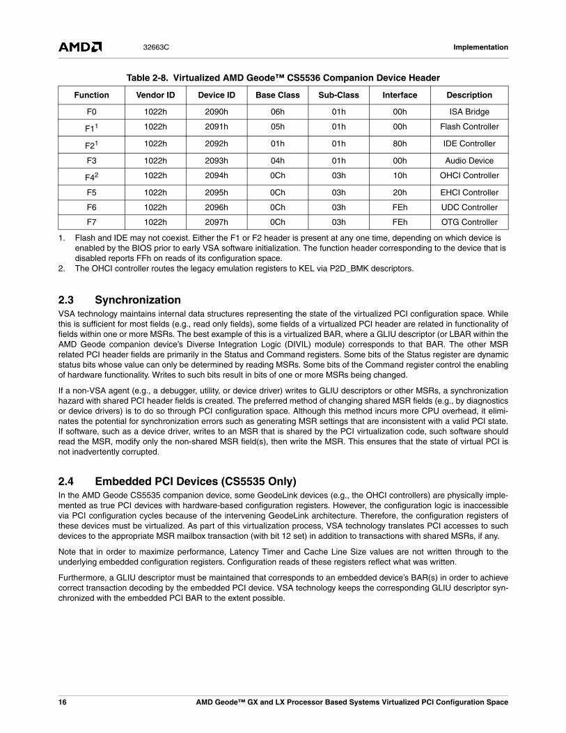
2.4 Embedded PCI Devices (CS5535 Only)In the AMD Geode CS5535 companion device, some GeodeLink devices (e.g., the OHCI controllers) are physically imple-mented as true PCI devices with hardware-based configuration registers. However, the configuration logic is inaccessiblevia PCI configuration cycles because of the intervening GeodeLink architecture. Therefore, the configuration registers ofthese devices must be virtualized. As part of this virtualization process, VSA technology translates PCI accesses to suchdevices to the appropriate MSR mailbox transaction (with bit 12 set) in addition to transactions with shared MSRs, if any.
Note that in order to maximize performance, Latency Timer and Cache Line Size values are not written through to theunderlying embedded configuration registers. Configuration reads of these registers reflect what was written.
Furthermore, a GLIU descriptor must be maintained that corresponds to an embedded device’s BAR(s) in order to achievecorrect transaction decoding by the embedded PCI device. VSA technology keeps the corresponding GLIU descriptor syn-chronized with the embedded PCI BAR to the extent possible.
Table 2-8. Virtualized AMD Geode™ CS5536 Companion Device Header
Function Vendor ID Device ID Base Class Sub-Class Interface Description
F0 1022h 2090h 06h 01h 00h ISA Bridge
F11
1. Flash and IDE may not coexist. Either the F1 or F2 header is present at any one time, depending on which device is enabled by the BIOS prior to early VSA software initialization. The function header corresponding to the device that is disabled reports FFh on reads of its configuration space.
1022h 2091h 05h 01h 00h Flash Controller
F21 1022h 2092h 01h 01h 80h IDE Controller
F3 1022h 2093h 04h 01h 00h Audio Device
F42
2. The OHCI controller routes the legacy emulation registers to KEL via P2D_BMK descriptors.
1022h 2094h 0Ch 03h 10h OHCI Controller
F5 1022h 2095h 0Ch 03h 20h EHCI Controller
F6 1022h 2096h 0Ch 03h FEh UDC Controller
F7 1022h 2097h 0Ch 03h FEh OTG Controller
16 AMD Geode™ GX and LX Processor Based Systems Virtualized PCI Configuration Space
PCI Header 32663C
33.0PCI Header
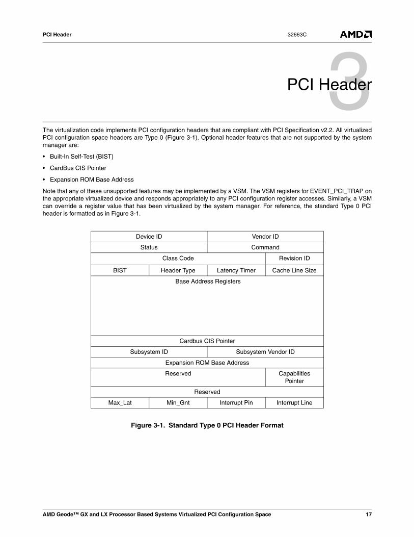
The virtualization code implements PCI configuration headers that are compliant with PCI Specification v2.2. All virtualizedPCI configuration space headers are Type 0 (Figure 3-1). Optional header features that are not supported by the systemmanager are:
• Built-In Self-Test (BIST)
• CardBus CIS Pointer
• Expansion ROM Base Address
Note that any of these unsupported features may be implemented by a VSM. The VSM registers for EVENT_PCI_TRAP onthe appropriate virtualized device and responds appropriately to any PCI configuration register accesses. Similarly, a VSMcan override a register value that has been virtualized by the system manager. For reference, the standard Type 0 PCIheader is formatted as in Figure 3-1.
Figure 3-1. Standard Type 0 PCI Header Format
Device ID Vendor ID
Status Command
Class Code Revision ID
BIST Header Type Latency Timer Cache Line Size
Base Address Registers
Cardbus CIS Pointer
Subsystem ID Subsystem Vendor ID
Expansion ROM Base Address
Reserved Capabilities Pointer
Reserved
Max_Lat Min_Gnt Interrupt Pin Interrupt Line
AMD Geode™ GX and LX Processor Based Systems Virtualized PCI Configuration Space 17

PCI Header32663C
3.1 Vendor IDAll virtualized PCI headers contain AMD’s vendor identifier (LX processor: 1022h; GX processor: 100Bh; CS5536 compan-ion device: 1022h; CS5535 companion device 100Bh).
3.2 Device IDThe Device ID field contains the vendor-specific ID assigned by AMD. The IDs for the various virtualized devices aredefined in Section 2.2 "Virtualized PCI Topology" on page 15.
3.3 Command RegisterThe Command register implements several bits that impact GeodeLink™ hardware.
3.3.1 I/O SpaceThis bit causes the descriptor(s) corresponding to all of the I/O BAR(s) associated with the virtualized PCI device to beeither disabled (bit = 0) or enabled (bit = 1). A descriptor is disabled by setting it to its default value. When enabled, adescriptor is written with a value corresponding to the last written BAR value, which is maintained in the VSA software PCItables. This bit is hardwired to 0 for devices that do not implement I/O BAR(s).
For bridge devices, changes to this bit only affect the BARs associated with the bridge function. That is, the I/O spaceenable does not affect the other functions in this device. Legacy I/O ranges are not affected by this bit.
3.3.2 Memory SpaceThis bit causes the descriptor(s) corresponding to all of the memory BAR(s) to be either disabled (bit = 0) or enabled (bit =1). A descriptor is disabled by setting it to its default value. When enabled, a descriptor is written with a value correspondingto the last written BAR value, which is maintained in VSA software PCI tables. This bit is hardwired to 0 for devices that donot implement memory BAR(s).
For bridge devices, changes to this bit only affect the BARs associated with the bridge function. That is, the I/O spaceenable does not affect the other functions in this device. Legacy memory ranges are not affected by this bit.
3.3.3 Bus MasterThis bit causes GLIU_PAE (MSR 51010081h) to be modified appropriately. If bus mastering is to be disabled, the fieldassociated with the port is cleared, else it is set to 3h. This bit is hardwired to zero for devices that are not bus masters.
For the Northbridge header, this bit is hardwired to 1. Writes do not have any effect. For the Southbridge header, this bit ishardwired to 0.
Bit Type Description
0 R/W I/O Space
1 R/W Memory Space
2 R/W Bus Master
3 RO Special Cycles
4 RO Memory Write and Invalidate Enable
5 RO VGA Palette Snoop
6 R/W Parity Error Response
7 RO Wait Cycle Control
8 R/W SERR# Enable
9 R/W Fast Back-to-Back Enable
18 AMD Geode™ GX and LX Processor Based Systems Virtualized PCI Configuration Space
PCI Header 32663C
3.3.4 Special CyclesThis bit is hardwired to 0 for all virtualized PCI devices except for the ISA bridge (F0 of the Southbridge header). TheAMD Geode companion device’s DIVIL (Diverse Integration Logic) module allows four responses to the Shutdown specialcycle:
• Perform a hard reset - controlled by the DIVIL_LEG_IO register (MSR Address 51400014h[31])
• Generate a GeodeLink Device error - controlled by the DIVIL_GLD_MSR_ERROR register (MSR Address 51400003h[15])
• Generate an ASMI - controlled by the DIVIL_GLD_MSR_SMI register (MSR Address 51400002h[1])
• Ignore (all three of the above responses are disabled)
When the Special Cycle Mode bit (MSR Address 51400014h[28]) is set in the ISA bridge function, MSR Address51400014h[31] is set, causing a reset on a Shutdown special cycle. When the Special Cycles bit is cleared, MSR51400014h[31] is cleared, causing Shutdown special cycles to be ignored. Before updating MSR Address 51400014h, VSAsoftware checks MSR 51400003h[15] and MSR 51400002h[1]. If either of these MSR bits are set, then no action is taken. Itis assumed that a debugger is being used and VSA does not interfere.
3.3.5 Memory Write and Invalidate EnableThe Memory Write and Invalidate command is not supported, so this bit is hardwired to 0 for all devices.
3.3.6 VGA Palette SnoopVGA palette snooping is not supported by the graphics hardware, so this bit is hardwired to 0.
3.3.7 Parity Error Response
This bit is implemented only for the ISA Bridge (Southbridge's F0), the Flash, ATA, and Audio devices, however, there areno linkages to MSRs.
3.3.8 Wait Cycle ControlSince the concept of address stepping does not apply to GeodeLink Devices, this bit is hardwired to 0.
3.3.9 SERR# EnableThis bit is hardwired to 0 since the SERR# signal is not supported.
3.3.10 Fast Back-to-Back EnableSince GeodeLink architecture supports the equivalent of Fast Back-to-Back transactions, this bit is hardwired to 1 for busmasters, else it is hardwired to 0.
AMD Geode™ GX and LX Processor Based Systems Virtualized PCI Configuration Space 19

PCI Header32663C
3.4 Status RegisterThe Status register is a mixture of static bits representing a device’s capabilities, and dynamic bits representing hardwarestatus.
When the Status register is read, bits 8 and [11:15] are set if the device is signaling the corresponding condition. The con-dition is not cleared until the Status register is written with a 1 in that bit position.
3.4.1 Capabilities ListSupport for the Capabilities List feature is architecturally supported by the PCI virtualization. If implemented, bit 4 of theStatus register is hardwired to 1, otherwise 0.
3.4.2 66 MHz CapableAll devices are marked as 66 MHz capable.
3.4.3 Fast Back-to-Back CapableDevices that are not bus masters have this bit hardwired to 0. AMD Geode companion devices are capable of accepting fastback-to-back transactions as a target. For these devices, this bit is hardwired to 1.
3.4.4 Data Parity Error DetectedThis bit is only implemented for bus master devices. If this bit is written with a 1, the Parity Error condition in cleared by writ-ing a 1 to the PARE_ERR_FLAG bit (GLPCI MSR Address 51000003h[21]).
3.4.4.1 DEVSEL# TimingAll headers reflect medium DEVSEL# timing.
3.4.5 Signaled Target-AbortThis bit is only implemented for the Northbridge and Southbridge headers. It is linked to MSR 51000003h[20].
Table 3-1. Status Register
Bit Type Value Description
0 RO1
1. Read only.
0 Reserved
1 RO 0 Reserved
2 RO 0 Reserved
3 RO 0 Reserved
4 RO 0 Capabilities List
5 RO 1 66 MHz capable
6 RO 0 Reserved
7 RO 0/1 Fast Back-to-Back Capable (1 for bus-masters; else 0)
8 R/C2
2. Read/Clear. The bit can be reset by writing a 1, but not set. Writing a 0 to this bit has no effect.
?3
3. Bit = 1 if condition is TRUE, else 0.
Data Parity Error Detected
9-10 RO 01 DEVSEL timing (Medium decode)
11 R/C ? Signaled Target-Abort
12 R/C ? Received Target-Abort
13 R/C ? Received Master-Abort
14 R/C ? Signaled System Error
15 R/C ? Detected Parity Error
20 AMD Geode™ GX and LX Processor Based Systems Virtualized PCI Configuration Space
PCI Header 32663C
3.4.6 Received Target-AbortThis bit is only implemented for the Northbridge and Southbridge headers. It is linked to MSR 51000003h[17].
3.4.7 Received Master-AbortThis bit is only implemented for the Northbridge and Southbridge headers. It is linked to MSR 51000003h[16].
3.4.8 Signaled System ErrorSince the AMD Geode processor and companion device do not implement the SERR# signal, this bit is not implemented(hardwired to 0).
3.4.9 Detected Parity ErrorThis bit is only implemented for the Northbridge and Southbridge headers. It is linked to MSR 51000003h[21].
3.5 Revision IDThis read only register reflects a device’s silicon revision.
3.6 Class CodeThe Class Code register is read only and is used to identify the generic functionality of the device. The class codes for thevarious virtualized devices are defined in Section 2.2 "Virtualized PCI Topology" on page 15.
3.7 Cache Line SizeThis register is hardwired to 08h for all other devices, signifying a 32-byte cache line. Per the PCI Specification, any unsup-ported value written to this register reads back as zero.
3.8 Latency TimerThis bit is implemented for the Northbridge and Southbridge headers only. For the bridge devices, the five MSBs are R/Wand are linked to the GLPCI_CTRL register (MSR 51000010h[39:35]). For the Northbridge, if the latency timer value iszeroed, MSR 50002010h[9] is zeroed. If the latency timer is subsequently written to a non-zero value, MSR 50002010h[9]is not modified.
3.9 Header TypeThis register is read only and has the value 00h, except for F0 of each virtualized bridge header, which reads 80h (multi-function device).
3.10 BISTThis read only register is treated as a reserved register (returns a value of zero) since a BIST (Built-In Self-Test) is optionaland is not supported by the system manager. If BIST support is desired, a VSM may be written to implement that function-ality.
Table 3-2. Revision ID Values
PCI Device Source of Revision ID
Northbridge GLCP_MSR 0017h[7:0]
Graphics GLD_MSR_CAP[7:0] of the GP
Southbridge GLCP_MSR 0017h[7:0]
OHCI Hardware PCI header of OHCI
All other devices GLD_MSR_CAP[7:0] for that device
AMD Geode™ GX and LX Processor Based Systems Virtualized PCI Configuration Space 21
PCI Header32663C
3.11 Base Address RegistersSince GeodeLink Device addresses are 32 bits, only memory BARs of Type 0 (located anywhere in 32-bit address space)are supported. All memory BARs are marked as non-prefetchable. Virtualizing PCI BARs requires more than recording val-ues on writes to PCI configuration space and returning those values on reads. Each time a BAR is changed, the corre-sponding GeodeLink MSR(s) must be modified. Table 3-3 shows the BAR usage for each function.
Note that the descriptor(s) corresponding to a BAR are not written until the memory space is enabled via the Commandregister. If a BAR is subsequently disabled via the Command register, the descriptor(s) corresponding to the affectedBAR(s) are written to their default values.
Notes:
• The Video and IDE functions contain legacy I/O ranges that are not reported by PCI BARs. These BARs are not linked to Command[0]. The resources are as follows:— Video:
– 128 KB memory @ A0000h-BFFFFh– 16 bytes of I/O @ 3C0h-3CFh– 16 bytes of I/O @ 3D0h-3DFh (or 3B0h-3BFh, if Mode 7)
— IDE– 8 bytes of I/O @ 1F0h-1F7h– 1 byte of I/O @ 3F6h
• If a BAR is written to zero (or is uninitialized), the associated descriptor(s) are not written when Command[1:0] are changed. This behavior is for compliance with the PCI Specification.
Table 3-3. BAR Usage Per Function
Device
Resource Requirements
AMD Geode™ GX Processor AMD Geode™ LX Processor
Host Bridge BAR0: 4 bytes I/O @ AC1C-AC1F (virtual registers) BAR0: 4 bytes I/O @ AC1C-AC1F (virtual registers)
Video BAR0: <n> MB memory (Frame buffer)
BAR1: 16 KB memory mapped I/O (GP)
BAR2: 16 KB memory mapped I/O (DC)
BAR3: 16 KB memory mapped I/O (VP)
BAR0: <n> MB memory (Frame buffer)
BAR1: 16 KB memory mapped I/O (GP)
BAR2: 16 KB memory mapped I/O (DC)
BAR3: 16 KB memory mapped I/O (VP)
BAR4: 16 KB memory mapped I/O (VIP)
ISA Bridge BAR0: 8 bytes I/O (SMB)
BAR1: 256 bytes I/O (GPIO)
BAR2: 64 bytes I/O (MFGPT)
BAR3: 32 bytes I/O (IRQ)
BAR4: 128 bytes I/O (PMS)
BAR5: 32 bytes I/O (ACPI)
BAR0: 8 byte I/O (SMB)
BAR1: 256 byte I/O (GPIO)
BAR2: 64 byte I/O (MFGPT)
BAR3: 32 byte I/O (IRQ)
BAR4: 128 byte I/O (PMS)
BAR5: 32 byte I/O (ACPI)
Flash BAR0: NOR Flash0: 4 KB memory mapped I/ONAND Flash0: 16 bytes I/O
BAR1: NOR Flash1: 4 KB memory mapped I/ONAND Flash1: 16 bytes I/O
BAR2: NOR Flash2: 4 KB memory mapped I/ONAND Flash2: 16 bytes I/O
BAR3: NOR Flash3: 4 KB memory mapped I/ONAND Flash3: 16 bytes I/O
BAR0: NOR Flash0: 4KB memory mapped I/ONAND Flash:0 16 byte I/O
BAR1: NOR Flash1: 4KB memory mapped I/ONAND Flash1: 16 byte I/O
BAR2: NOR Flash2: 4KB memory mapped I/ONAND Flash2: 16 byte I/O
BAR3: NOR Flash3: 4KB memory mapped I/ONAND Flash3: 16 byte I/O
IDE BAR4: 8 bytes I/O BAR4: 8 bytes I/O
Audio BAR0: 128 bytes of I/O BAR0: 128 bytes of I/O
USB OHCI #1 - BAR0: 4 KB memory mapped I/OOHCI #2 - BAR0: 4 KB memory mapped I/O
OHCI - BAR0: 4 KB memory mapped I/OEHCI - BAR0: 4 KB memory mapped I/OUDC - BAR0: 4 KB memory mapped I/OOTG - BAR0: 4 KB memory mapped I/O
AES NA - AMD Geode LX processor only BAR0: 16 KB memory mapped I/O
22 AMD Geode™ GX and LX Processor Based Systems Virtualized PCI Configuration Space
PCI Header 32663C
3.12 Subsystem Vendor IDThe Subsystem Vendor ID field matches the Vendor ID field.
3.13 Subsystem IDThe Subsystem ID field matches the Device ID field.
3.14 Capabilities PointerThis read only register contains the DWORD aligned register value of the first capabilities record.
3.15 Interrupt LineThe Interrupt Line register is implemented for those devices that use an interrupt pin. It provides no hardware functionality.It is used by POST to communicate interrupt line routing information to an operating system.
3.16 Interrupt PinThe Interrupt Pin register is implemented for those functions that may assert a PCI interrupt pin. Those devices that do notuse an interrupt pin return 00h in this register. This register is read only.
3.17 Min_Gnt RegisterThe Min_Gnt register is a read only register. For devices that are not bus masters, this register reads 00h. For bus master-ing devices, this register conveys the appropriate timing information.
3.18 Max_Lat RegisterThe Max_Lat register is a read only register. For devices that are not bus masters, this register reads 00h. For bus master-ing devices, this register conveys the appropriate timing information.
3.19 OEM RegistersThe Virtual PCI implementation is designed to support OEM defined PCI registers.
• PCI interrupt steering registers at 785Ch-785Dh.
• Software SMI register at 78D0h.
• Switch to IDE header at 7940h.
• Switch to Flash header at 7A40h.
• IDE Channel presence at 7A44h.
• SoftVG diagnostic register at 9044h.
Other OEM registers may be implemented by VSMs as required by individual platforms.
AMD Geode™ GX and LX Processor Based Systems Virtualized PCI Configuration Space 23

PCI Header32663C
24 AMD Geode™ GX and LX Processor Based Systems Virtualized PCI Configuration Space

PCI Interrupts 32663C
44.0PCI Interrupts
4.1 PCI Interrupt SteeringThe PCI interrupt steering registers are implemented at Southbridge F0 registers 5Ch-5Dh. The register layout is:
Each 4-bit field selects an IRQ:0000 = Disable 0100 = IRQ4 1000 = IRQ8 1100 = IRQ120001 = IRQ1 0101 = IRQ5 1001 = IRQ9 1101 = IRQ130010 = RSVD 0110 = IRQ6 1010 = IRQ10 1110 = IRQ140011 = IRQ3 0111 = IRQ7 1011 = IRQ11 1111 = IRQ15
By default, the PCI interrupts are assigned to GPIO pins as:INTA#: GPIO0INTB#: GPIO7INTC#: GPIO12INTD#: GPIO13
The GPIOs assigned to PCI interrupts are configured as level-sensitive, inverted inputs.
If a platform uses a different configuration, the BIOS must notify VSA software of the new pin assignments. They may notbe changed more than once. Subsequent attempts to change them are ignored.
Note: Changing GPIO pin assignments must be done before the Interrupt Steering register is written.
To change the GPIOs assigned to INTA# and INTB#, execute the following code:MOV DX, 0AC1ChMOV AX, 0FC53h ; Unlock virtual registerOUT DX, AXMOV AH, 00h ; Class = VRC_MISCELLANEOUSMOV AL, 09h ; Index = PCI_INT_ABOUT DX, AX ; Write Class:IndexADD DL, 2 ; Point to Virtual Register Data portMOV AL, 08h ; Use GPIO pin 8 for INTA#MOV AH, 09h ; Use GPIO pin 9 for INTB#OUT DX, AX
Register Bits Description
785Ch 3:0 Selects the target IRG for INTA#
785Ch 7:4 Selects the target IRG for INTB#
785Dh 3:0 Selects the target IRG for INTC#
785Dh 7:4 Selects the target IRG for INTD#
AMD Geode™ GX and LX Processor Based Systems Virtualized PCI Configuration Space 25

PCI Interrupt Steering32663C
Similarly, to change the GPIO pin assignments for INTC# and INTD#:MOV DX, 0AC1ChMOV AX, 0FC53h ; Unlock virtual registerOUT DX, AXMOV AH, 00h ; Class = VRC_MISCELLANEOUSMOV AL, 0Ah ; Index = PCI_INT_CDOUT DX, AX ; Write Class::IndexADD DL, 2 ; Point to Virtual Register Data portMOV AL, 10h ; Use GPIO pin 10h for INTC#MOV AH, 0Fh ; Use GPIO pin 0Fh for INTD#OUT DX, AX
If a platform does not require four PCI interrupts, the BIOS may reduce the number of PCI interrupts supported. This isdone by assigning a pin # greater than or equal to 20h. If a virtualized PCI header uses an interrupt pin for which a GPIOpin is no longer assigned, that Interrupt Pin register is reduced to the next lower valid value. For example, if support forINTC# and INTD# are removed (by writing 0FFFFh to virtual register 000Ah), then all virtualized PCI headers that previ-ously defined either INTC# or INTD# are changed to INTB#.
26 AMD Geode™ GX and LX Processor Based Systems Virtualized PCI Configuration Space

VSM Support 32663C
55.0VSM Support
Three system calls are provided to assist VSMs with GeodeLink™ architecture issues. Additionally, a virtual register hasbeen added for use by non-VSA software for determining the information about the BAR to descriptor mapping.
PCI trapping is performed when a VSM specifically requests it via a call to SYS_REGISTER_EVENT(EVENT_PCI_TRAP,…). On a trapped access to CFCh, the system manager virtualizes the standard header registers. It then passes theEVENT_PCI_TRAP to VSM(s) that have registered for that PCI configuration address. This functionality is typically onlyused by VSMs that:
• Monitor accesses to virtualized registers.
• Modify the standard virtualized values.
• Implement device dependent registers 40h-FFh.
The WRITE_PCI_xxxx_NO_TRAP and READ_PCI_xxxx_NO_TRAP macros behave differently for virtualized headersthan for hardware based headers. As the macro names implies, a PCI access using these macros normally would disablePCI trapping, perform the access to the underlying PCI header, and re-enable trapping. However, for virtualized headers,since there is no underlying PCI header hardware (the AMD Geode companion device has a minimal header), such amethod does not suffice. Therefore, these macros are implemented the same as WRITE_PCI_xxxx and READ_PCI_xxxxfor virtualized headers.
5.1 SYS_LOOKUP_DEVICEIf a VSM must write to device MSRs, the MSR routing bits must be determined. Since these addresses might change onfuture AMD Geode device implementations, it is good programming practice for a VSM to hard-code this addressing infor-mation. A macro is supplied that scans the GeodeLink topology for a particular Device ID and returns the routing address.The VSM can use this routing address to directly access device MSRs.
The macro requires two parameters (both unsigned short):
1) GeodeLink Device ID
2) Instance – normally 1, unless there are multiple devices of the same type (e.g., OHCI, GLIU)
The macro returns an unsigned long with the routing information (x.x.x.x.x.x format) of the requested device. If the devicewas not found, 00000000h is returned.
Sample usage:unsigned long Routing;
// Scan for the memory controller
Routing = SYS_LOOKUP_DEVICE(0x0020, 1);
AMD Geode™ GX and LX Processor Based Systems Virtualized PCI Configuration Space 27

VSM Support32663C
5.2 SYS_ALLOCATE_RESOURCEVSMs controlling a device that is represented by a virtualized PCI configuration header must associate one or moredescriptors with the appropriate GLIU port(s). In order to assist the VSM in this task, a macro is provided to VSMs that:
• Instructs the system manager of the BAR type (I/O or memory) and resource requirements for a BAR
• Relieves the VSMs of scanning the GeodeLink interface for the device in question
• Relieves the VSM of handling the details of GLIU descriptor setup
• Allows the system manager to act as a centralized descriptor allocator
• Allows the system manager to define the virtual PCI topology
The SYS_ALLOCATE_RESOURCE macro requires five parameters:
• unsigned char P1: <RESOURCE_MEMORY | RESOURCE_MMIO | RESOURCE_IO | RESOURCE_SCIO>
• unsigned char P2: BAR address to allocate (10h through 24h, DWORD aligned)
• unsigned long P3: Memory or I/O range (or mask if P1 == RESOURCE_SCIO)
• unsigned short P4: PCI Device ID
• unsigned short P5: GeodeLink Device ID
The first parameter (P1) specifies what type of resource is requested. RESOURCE_MEMORY should be used when phys-ical memory needs to be allocated, as in a video frame buffer. RESOURCE_MMIO is for devices that are controlled throughmemory-mapped I/O. RESOURCE_IO is for devices that require addresses within I/O space to be routed to the appropriatedevice. RESOURCE_SCIO is used when a discontiguous I/O range is required, thus requiring a Swiss-cheese descriptor tobe used. In this case, P3 is an 8-bit mask, where a 1 specifies an I/O byte that is to be considered part of the I/O range.
In each case, one or more descriptors to the appropriate GLIUs, LBARs, and/or RCONFs are allocated. The assigneddescriptor(s) are not actually initialized until the BAR is written and the corresponding address space (memory or I/O) isenabled via the PCI Command register.
The second parameter (P2) specifies which BAR is being defined. If the BAR is to be hidden (as for VGA legacyaddresses), this parameter should be ORed with HIDE_BAR. This causes the BAR to contain 00000000h and it will notreport resource requirements. The BAR otherwise functions as a regular BAR (e.g., it may be disabled or enabled via theCommand register).
The third parameter (P3) defines the size of the requested resource. The units are in bytes. For RESOURCE_MMIO,ranges are rounded up to at least 4 KB due to the granularity of GLIU descriptors. For RESOURCE_SCIO, this parameteris a mask that defines which I/O locations are to be routed - one bit per I/O location, starting at the BAR address. Discontig-uous I/O ranges are handled with IOD_SC (Swiss-cheese) I/O descriptors. In order to comply with the PCI Specification,range, requirements are rounded up to the next power of two that encompasses the entire range.
The fourth parameter (P4) specifies the AMD PCI Device ID with which the virtualized BAR is to be associated.
The fifth parameter (P5) specifies the physical GeodeLink Device ID to which the BAR resource is to be associated. Thisparameter is used to determine the appropriate routing information for the underlying descriptor.
The macro returns an unsigned long containing the PCI configuration address assigned to the BAR. For example, if arequest is made for a BAR0 associated with the DC device, the value 80000910h is returned. This is interpreted as the vir-tualized Device Number 1, Function 1. This parameter may be used for registering EVENT_PCI_TRAP or accessing the vir-tualized PCI device via the READ_PCI and WRITE_PCI macros.
Sample Usage:// Associate GeodeLink device 0x3E (Video Generator) with BAR0 of PCI Device ID 0x0030 (Graphics device)
PCI_Address = SYS_ALLOCATE_RESOURCE(RESOURCE_MMIO, 0x10, 0x1000, 0x0030, 0x003E);
Note: As with a hardware PCI BAR, setting of the base address occurs when the BAR is written. Therefore, VSMs thatcorrespond to virtualized boot devices must define all of their PCI resource requirements before the BIOS scansthe PCI bus (early VSA initialization, not end-of-POST initialization).
28 AMD Geode™ GX and LX Processor Based Systems Virtualized PCI Configuration Space
VSM Support 32663C
5.3 SYS_GET_DESCRIPTORIf a VSM needs to read a descriptor MSR associated with one of its BARs, the SYS_GET_DESCRIPTOR macro is pro-vided. The macro takes one parameter, the PCI BAR address. The macro returns an unsigned long with the MSR addressof the descriptor associated with the BAR.
Sample Usage:ULONG Descriptor[2];ULONG PCI_Address;
PCI_Address = <virtualized PCI BAR address>SYS_GET_DESCRIPTOR(PCI_Address, Descriptor);
5.4 GET_DESCR_INFOA new virtual register in class VRC_MISCELLANEOUS (00h) has been added for the occasions when a device driver orother software needs to access a descriptor corresponding to a virtualized PCI BAR. The index is GET_DESCR_INFO(08h). When the 16 LSBs of a virtualized PCI address are written to this register, ECX is set to the MSR address of the cor-responding descriptor. Registers EDX:EAX are set to the contents of this MSR. Register BL is set to a code indicating thetype of descriptor as follows:
P2D_BM 1P2D_R 2P2D_BMO 3P2D_RO 4P2D_SC 5P2D_SCO 6P2D_BMK 7IOD_BM 8IOD_SC 9
5.5 SYS_MAP_IRQSYS_MAP_IRQ(unsigned char Source, unsigned char Irq)
If a VSM requires unrestricted Y Sources (IRQ Mapper inputs) to be routed, the SYS_MAP_IRQ macro is provided. Thefirst parameter is the number of the Y Source to be mapped. The second parameter is the IRQ to which the Y Source is tobe mapped. To disable a Y Source mapping, set IRQ to zero. To route a Y Source to an SMI, set IRQ to 2.
Sample Usage:// Map SCIs to SMISYS_MAP_IRQ(5, 2);
AMD Geode™ GX and LX Processor Based Systems Virtualized PCI Configuration Space 29

VSM Support32663C
30 AMD Geode™ GX and LX Processor Based Systems Virtualized PCI Configuration Space
Appendix A: Support Documentation 32663C
Appendix ASupport Documentation
The tables in Section A.1 "AMD Geode™ GX Processor/CS5535 Companion Device MSR Address Values" and SectionA.2 "AMD Geode™ LX Processor/CS5536 Companion Device MSR Address Values" on page 39 show typical MSRAddress values for some of the PCI Addresses.
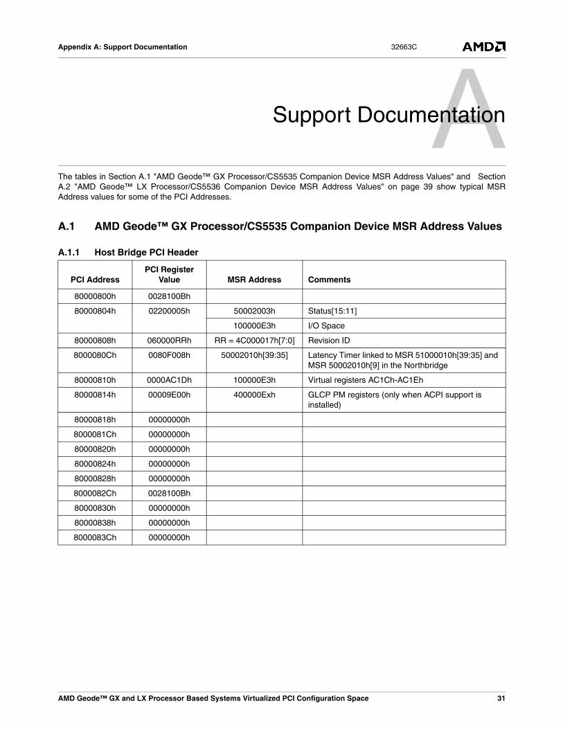
A.1 AMD Geode™ GX Processor/CS5535 Companion Device MSR Address Values
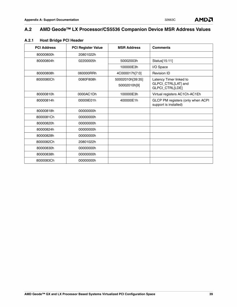
A.1.1 Host Bridge PCI Header
PCI AddressPCI Register
Value MSR Address Comments
80000800h 0028100Bh
80000804h 02200005h 50002003h Status[15:11]
100000E3h I/O Space
80000808h 060000RRh RR = 4C000017h[7:0] Revision ID
8000080Ch 0080F008h 50002010h[39:35] Latency Timer linked to MSR 51000010h[39:35] and MSR 50002010h[9] in the Northbridge
80000810h 0000AC1Dh 100000E3h Virtual registers AC1Ch-AC1Eh
80000814h 00009E00h 400000Exh GLCP PM registers (only when ACPI support is installed)
80000818h 00000000h
8000081Ch 00000000h
80000820h 00000000h
80000824h 00000000h
80000828h 00000000h
8000082Ch 0028100Bh
80000830h 00000000h
80000838h 00000000h
8000083Ch 00000000h
AMD Geode™ GX and LX Processor Based Systems Virtualized PCI Configuration Space 31
Appendix A: Support Documentation32663C
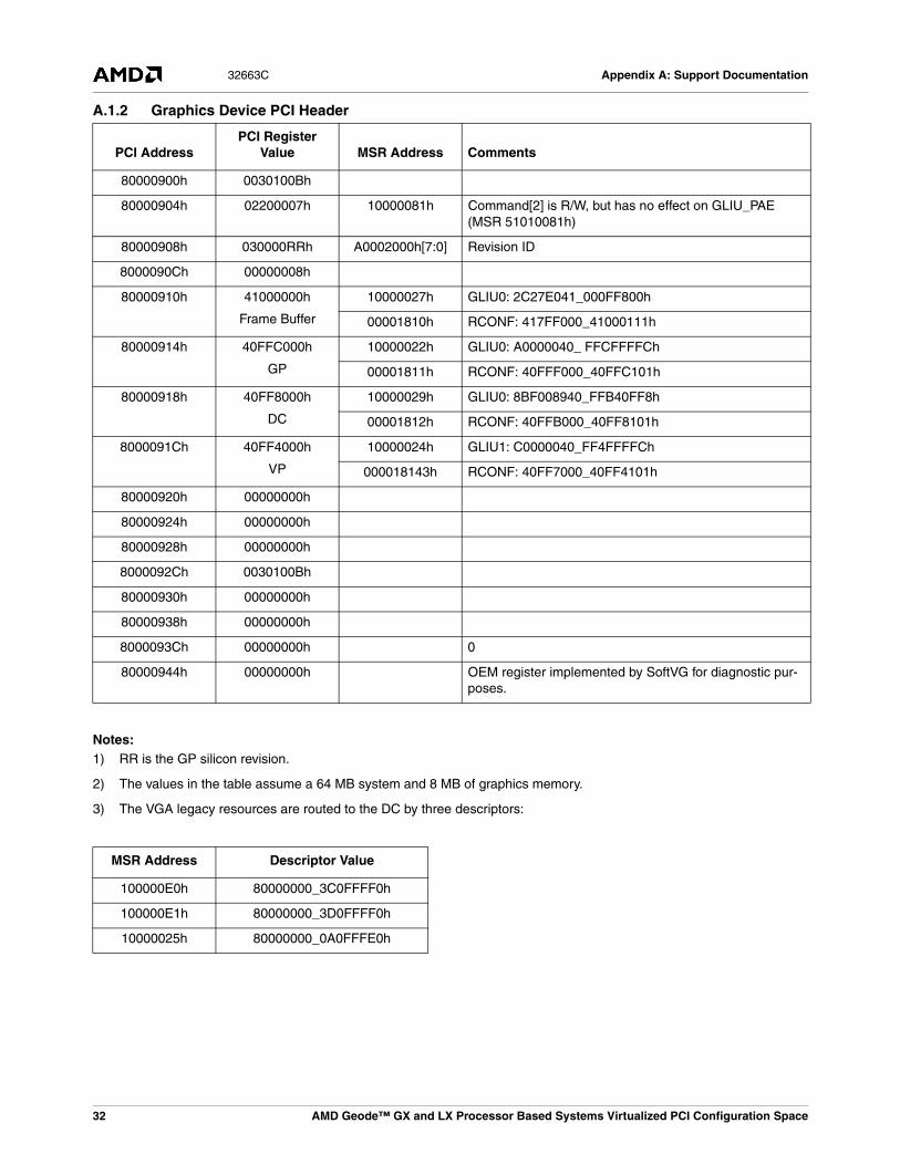
A.1.2 Graphics Device PCI Header
Notes:1) RR is the GP silicon revision.
2) The values in the table assume a 64 MB system and 8 MB of graphics memory.
3) The VGA legacy resources are routed to the DC by three descriptors:
PCI AddressPCI Register
Value MSR Address Comments
80000900h 0030100Bh
80000904h 02200007h 10000081h Command[2] is R/W, but has no effect on GLIU_PAE (MSR 51010081h)
80000908h 030000RRh A0002000h[7:0] Revision ID
8000090Ch 00000008h
80000910h 41000000h
Frame Buffer
10000027h GLIU0: 2C27E041_000FF800h
00001810h RCONF: 417FF000_41000111h
80000914h 40FFC000h
GP
10000022h GLIU0: A0000040_ FFCFFFFCh
00001811h RCONF: 40FFF000_40FFC101h
80000918h 40FF8000h
DC
10000029h GLIU0: 8BF008940_FFB40FF8h
00001812h RCONF: 40FFB000_40FF8101h
8000091Ch 40FF4000h
VP
10000024h GLIU1: C0000040_FF4FFFFCh
000018143h RCONF: 40FF7000_40FF4101h
80000920h 00000000h
80000924h 00000000h
80000928h 00000000h
8000092Ch 0030100Bh
80000930h 00000000h
80000938h 00000000h
8000093Ch 00000000h 0
80000944h 00000000h OEM register implemented by SoftVG for diagnostic pur-poses.
MSR Address Descriptor Value
100000E0h 80000000_3C0FFFF0h
100000E1h 80000000_3D0FFFF0h
10000025h 80000000_0A0FFFE0h
32 AMD Geode™ GX and LX Processor Based Systems Virtualized PCI Configuration Space

Appendix A: Support Documentation 32663C
A.1.3 AMD Geode™ CS5535 Southbridge PCI HeadersThe CS5535 Southbridge header consists of six virtualized PCI functions:
F0 - ISA Bridge
F1 - Flash Controller
F2 - IDE Controller
F3 - Audio Device
F4 - USB Controller #1 (OHCI)
F5 - USB Controller #2 (OHCI)
Table A-1. Standard PCI Header for F0 - ISA Bridge
PCI AddressPCI Register
Value MSR Address Comments
80007800h 002B100Bh
80007804h 02A00009h 51102003h Status[15:11]
51402014h[31] Special Cycles
I/O Space - linked to LBAR_EN of BARs
80007808h 060100RRh 51700017h[7:0] Revision ID
8000780Ch 0080F008h 51002010h[39:35] Latency Timer
80007810h 00006001h 5140200Bh
51000020h
SMB LBAR = 0000F001_00006000h
GLPCI RCONF = 06004001_06000001h
80007814h 00006101h 5140200Ch
51000021h
GPIO LBAR = 0000F001_00006100h
GLPCI RCONF = 061FC00_06100001h
80007818h 00006201h 5140200Dh
51000022h
MFGPT LBAR = 0000F001_00006200h
GLPCI RCONF = 0623C001_06200001h
8000781Ch 00000001h 51402008h
51000023h
IRQ LBAR = 00000000_00000000h
GLPCI RCONF = 00000000_00000000h
80007820h 00009D01h 5140200Fh
51000024h
PMS LBAR = 0000F001_00009D00h
GLPCI RCONF = 09D7C001_09D00001h
80007824h 00009C01h 5140200Eh
51000025h
ACPI LBAR = 0000F001_00009C00h
GLPCI RCONF = 09C3C001_09C00001h
80007828h 00000000h
8000782Ch 002B100Bh
80007830h 00000000h
80007838h 00000000h
8000783Ch 00000000h
AMD Geode™ GX and LX Processor Based Systems Virtualized PCI Configuration Space 33
Appendix A: Support Documentation32663C
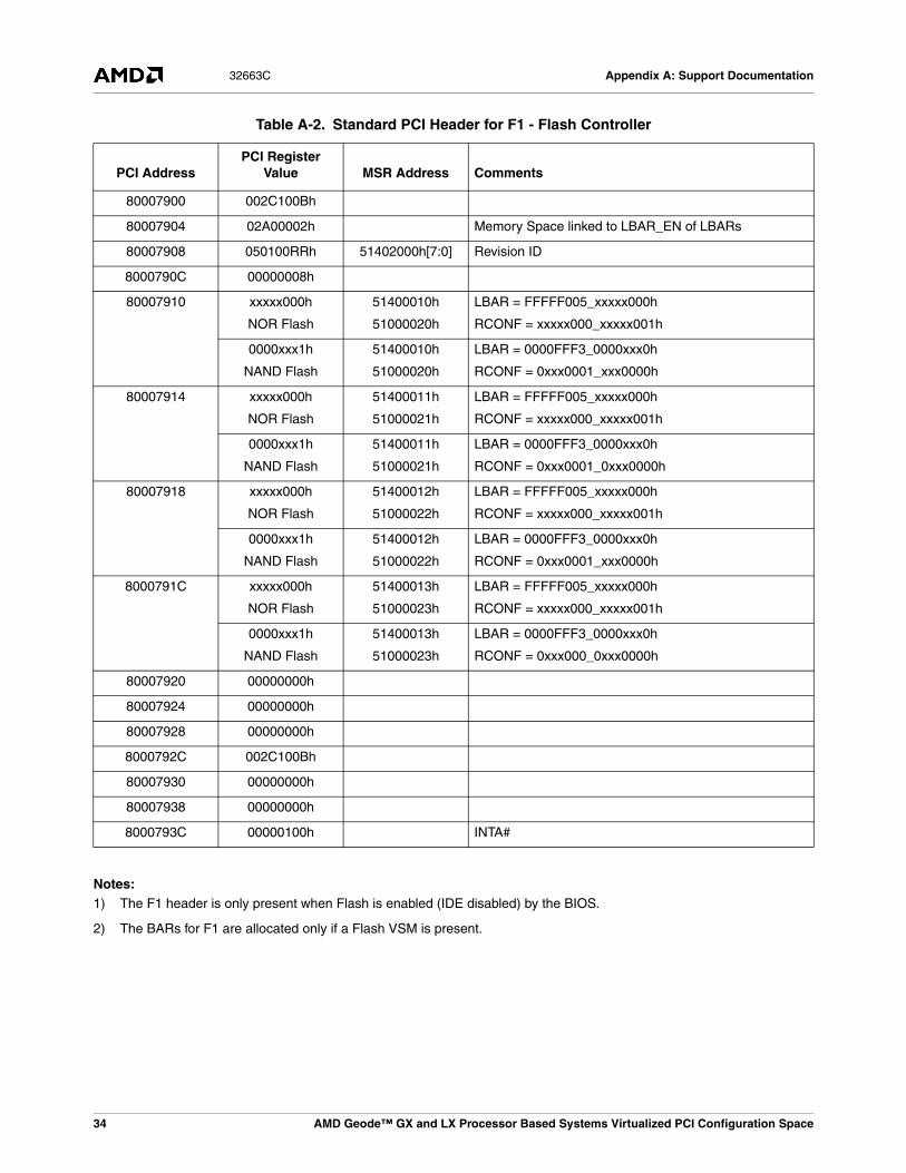
Notes:1) The F1 header is only present when Flash is enabled (IDE disabled) by the BIOS.
2) The BARs for F1 are allocated only if a Flash VSM is present.
Table A-2. Standard PCI Header for F1 - Flash Controller
PCI AddressPCI Register
Value MSR Address Comments
80007900 002C100Bh
80007904 02A00002h Memory Space linked to LBAR_EN of LBARs
80007908 050100RRh 51402000h[7:0] Revision ID
8000790C 00000008h
80007910 xxxxx000h
NOR Flash
51400010h
51000020h
LBAR = FFFFF005_xxxxx000h
RCONF = xxxxx000_xxxxx001h
0000xxx1h
NAND Flash
51400010h
51000020h
LBAR = 0000FFF3_0000xxx0h
RCONF = 0xxx0001_xxx0000h
80007914 xxxxx000h
NOR Flash
51400011h
51000021h
LBAR = FFFFF005_xxxxx000h
RCONF = xxxxx000_xxxxx001h
0000xxx1h
NAND Flash
51400011h
51000021h
LBAR = 0000FFF3_0000xxx0h
RCONF = 0xxx0001_0xxx0000h
80007918 xxxxx000h
NOR Flash
51400012h
51000022h
LBAR = FFFFF005_xxxxx000h
RCONF = xxxxx000_xxxxx001h
0000xxx1h
NAND Flash
51400012h
51000022h
LBAR = 0000FFF3_0000xxx0h
RCONF = 0xxx0001_xxx0000h
8000791C xxxxx000h
NOR Flash
51400013h
51000023h
LBAR = FFFFF005_xxxxx000h
RCONF = xxxxx000_xxxxx001h
0000xxx1h
NAND Flash
51400013h
51000023h
LBAR = 0000FFF3_0000xxx0h
RCONF = 0xxx000_0xxx0000h
80007920 00000000h
80007924 00000000h
80007928 00000000h
8000792C 002C100Bh
80007930 00000000h
80007938 00000000h
8000793C 00000100h INTA#
34 AMD Geode™ GX and LX Processor Based Systems Virtualized PCI Configuration Space
Appendix A: Support Documentation 32663C
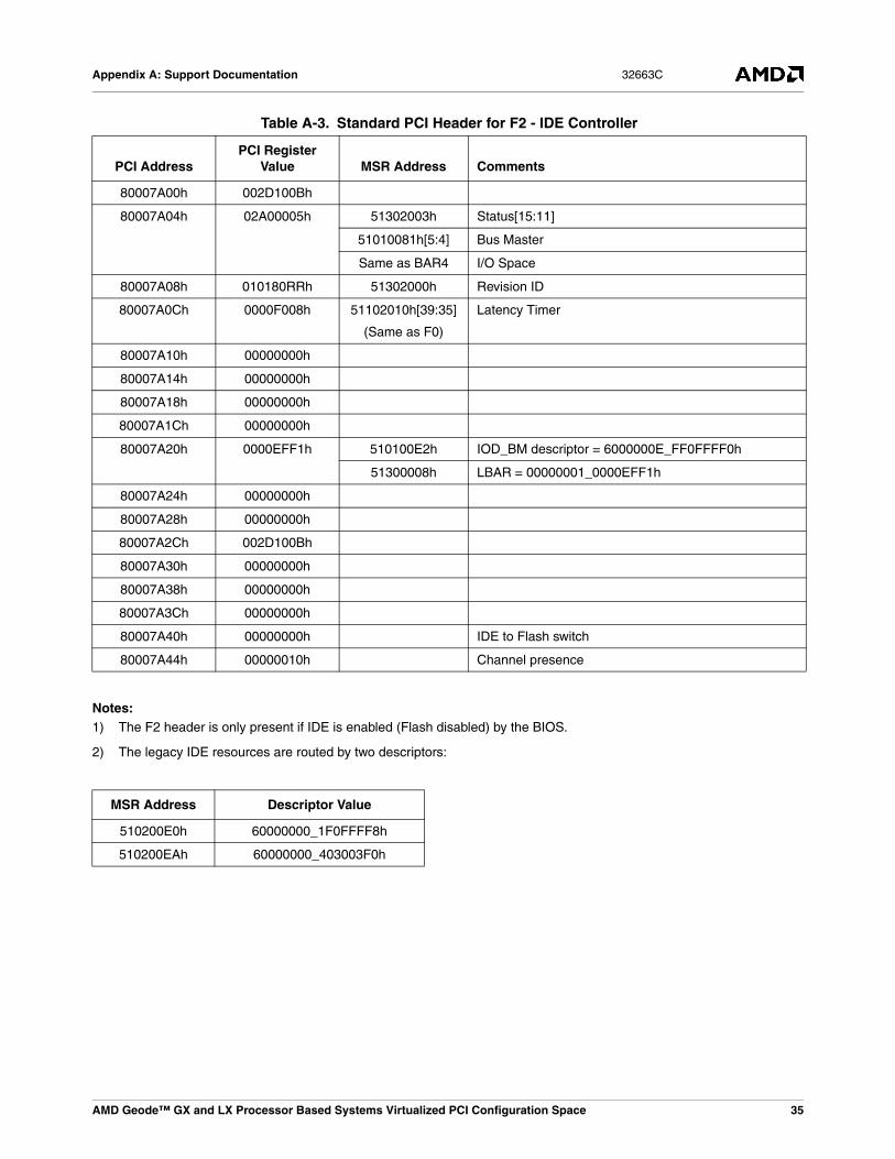
Notes:1) The F2 header is only present if IDE is enabled (Flash disabled) by the BIOS.
2) The legacy IDE resources are routed by two descriptors:
Table A-3. Standard PCI Header for F2 - IDE Controller
PCI AddressPCI Register
Value MSR Address Comments
80007A00h 002D100Bh
80007A04h 02A00005h 51302003h Status[15:11]
51010081h[5:4] Bus Master
Same as BAR4 I/O Space
80007A08h 010180RRh 51302000h Revision ID
80007A0Ch 0000F008h 51102010h[39:35]
(Same as F0)
Latency Timer
80007A10h 00000000h
80007A14h 00000000h
80007A18h 00000000h
80007A1Ch 00000000h
80007A20h 0000EFF1h 510100E2h IOD_BM descriptor = 6000000E_FF0FFFF0h
51300008h LBAR = 00000001_0000EFF1h
80007A24h 00000000h
80007A28h 00000000h
80007A2Ch 002D100Bh
80007A30h 00000000h
80007A38h 00000000h
80007A3Ch 00000000h
80007A40h 00000000h IDE to Flash switch
80007A44h 00000010h Channel presence
MSR Address Descriptor Value
510200E0h 60000000_1F0FFFF8h
510200EAh 60000000_403003F0h
AMD Geode™ GX and LX Processor Based Systems Virtualized PCI Configuration Space 35

Appendix A: Support Documentation32663C
Table A-4. Standard PCI Header for F3 - Audio Device
PCI AddressPCI Register
Value MSR Address Comments
80007B00h 002E100Bh
80007B04h
02A00005h
51502003h Status[15:11]
51010081h[9:8] Bus Master
Same as BAR0 I/O Space
80007B08h 040100RRh 51502000h Revision ID
80007B0Ch 00000008h
80007B10h 0000EF01h 510100E1h IOD_BM descriptor = A000000E_F00FFF80h
80007B14h 00000000h
80007B18h 00000000h
80007B1Ch 00000000h
80007B20h 00000000h
80007B24h 00000000h
80007B28h 00000000h
80007B2Ch 002E100Bh
80007B30h 00000000h
80007B38h 00000000h
80007B3Ch 00000200h INTB#
36 AMD Geode™ GX and LX Processor Based Systems Virtualized PCI Configuration Space
Appendix A: Support Documentation 32663C
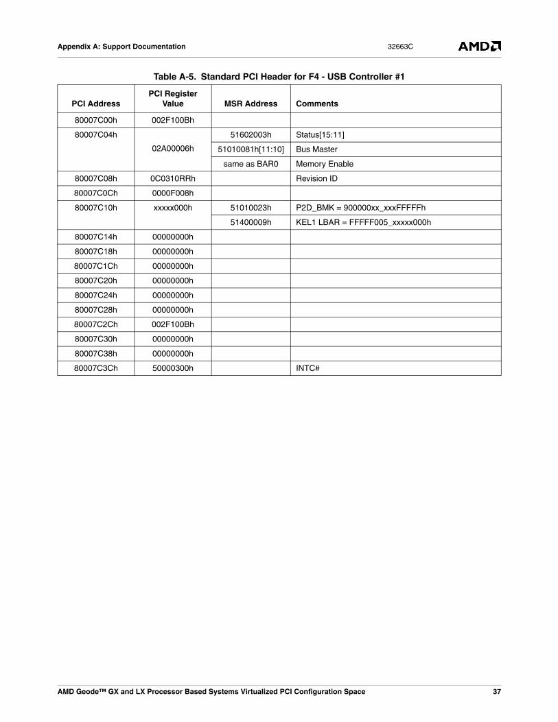
Table A-5. Standard PCI Header for F4 - USB Controller #1
PCI AddressPCI Register
Value MSR Address Comments
80007C00h 002F100Bh
80007C04h
02A00006h
51602003h Status[15:11]
51010081h[11:10] Bus Master
same as BAR0 Memory Enable
80007C08h 0C0310RRh Revision ID
80007C0Ch 0000F008h
80007C10h xxxxx000h 51010023h P2D_BMK = 900000xx_xxxFFFFFh
51400009h KEL1 LBAR = FFFFF005_xxxxx000h
80007C14h 00000000h
80007C18h 00000000h
80007C1Ch 00000000h
80007C20h 00000000h
80007C24h 00000000h
80007C28h 00000000h
80007C2Ch 002F100Bh
80007C30h 00000000h
80007C38h 00000000h
80007C3Ch 50000300h INTC#
AMD Geode™ GX and LX Processor Based Systems Virtualized PCI Configuration Space 37

Appendix A: Support Documentation32663C
Table A-6. Standard PCI Header for F5 - USB Controller #2
PCI Address PCI Register Value MSR Address Comments
80007D00h 002F100Bh
80007D04h
02A00006h
51202003h Status[15:11]
51010081h[3:2] Bus Master
Same as BAR0 Memory Enable
80007D08h 0C0310RRh Revision ID
80007D0Ch 0000F008h
80007D10h xxxxx000h 51010024h P2D_BMK = 900000xx_xxxFFFFFh
80007D14h 00000000h
80000DC8h 00000000h
80007D1Ch 00000000h
80007D20h 00000000h
80007D24h 00000000h
80007D28h 00000000h
80007D2Ch 002F100Bh
80007D30h 00000000h
80007D38h 00000000h
80007D3Ch 50000400h INTD#
38 AMD Geode™ GX and LX Processor Based Systems Virtualized PCI Configuration Space
Appendix A: Support Documentation 32663C
A.2 AMD Geode™ LX Processor/CS5536 Companion Device MSR Address Values
A.2.1 Host Bridge PCI Header
PCI Address PCI Register Value MSR Address Comments
80000800h 20801022h
80000804h 02200005h 50002003h Status[15:11]
100000E3h I/O Space
80000808h 060000RRh 4C000017h[7:0] Revision ID
8000080Ch 0080F808h 50002010h[39:35]
50002010h[9]
Latency Timer linked to GLPCI_CTRL[LAT] and GLPCI_CTRL[LDE]
80000810h 0000AC1Dh 100000E3h Virtual registers AC1Ch-AC1Eh
80000814h 00009E01h 400000E1h GLCP PM registers (only when ACPI support is installed)
80000818h 00000000h
8000081Ch 00000000h
80000820h 00000000h
80000824h 00000000h
80000828h 00000000h
8000082Ch 20801022h
80000830h 00000000h
80000838h 00000000h
8000083Ch 00000000h
AMD Geode™ GX and LX Processor Based Systems Virtualized PCI Configuration Space 39
Appendix A: Support Documentation32663C
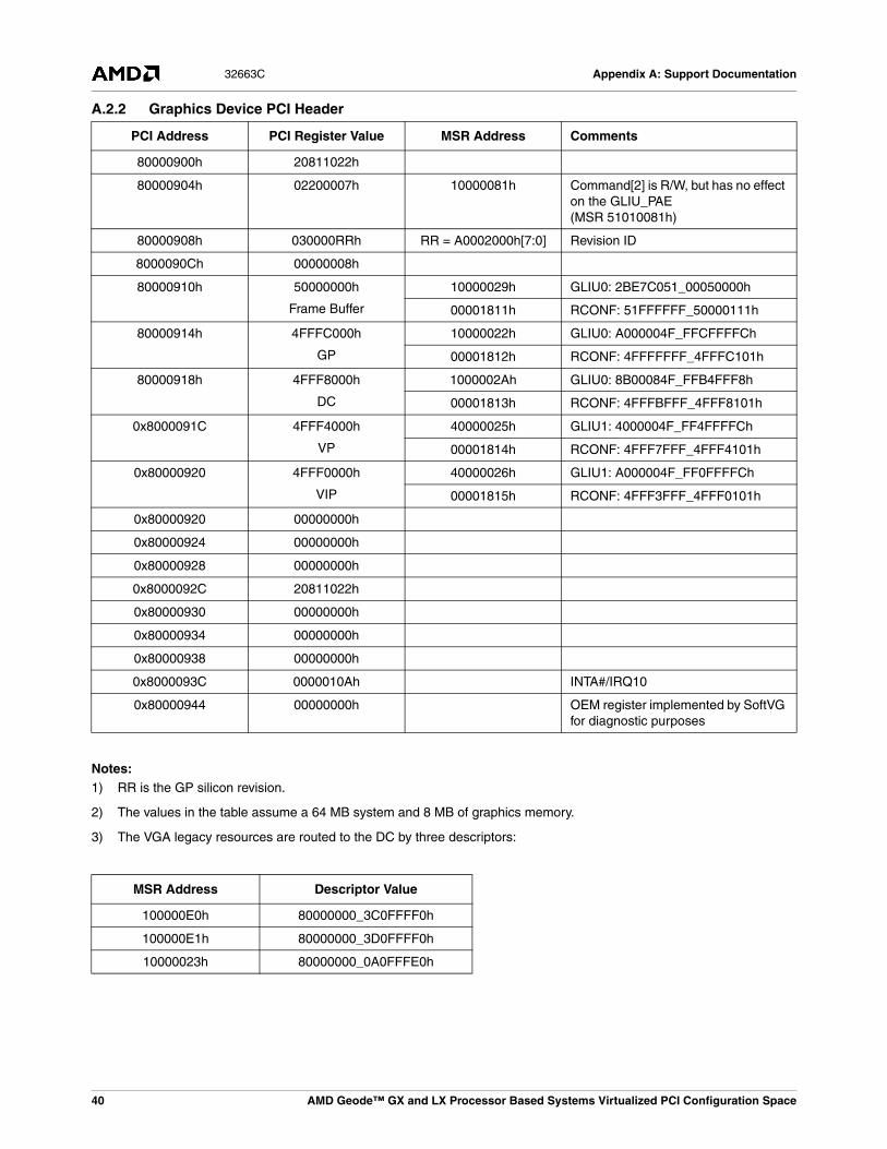
A.2.2 Graphics Device PCI Header
Notes:1) RR is the GP silicon revision.
2) The values in the table assume a 64 MB system and 8 MB of graphics memory.
3) The VGA legacy resources are routed to the DC by three descriptors:
PCI Address PCI Register Value MSR Address Comments
80000900h 20811022h
80000904h 02200007h 10000081h Command[2] is R/W, but has no effect on the GLIU_PAE (MSR 51010081h)
80000908h 030000RRh RR = A0002000h[7:0] Revision ID
8000090Ch 00000008h
80000910h 50000000h
Frame Buffer
10000029h GLIU0: 2BE7C051_00050000h
00001811h RCONF: 51FFFFFF_50000111h
80000914h 4FFFC000h
GP
10000022h GLIU0: A000004F_FFCFFFFCh
00001812h RCONF: 4FFFFFFF_4FFFC101h
80000918h 4FFF8000h
DC
1000002Ah GLIU0: 8B00084F_FFB4FFF8h
00001813h RCONF: 4FFFBFFF_4FFF8101h
0x8000091C 4FFF4000h
VP
40000025h GLIU1: 4000004F_FF4FFFFCh
00001814h RCONF: 4FFF7FFF_4FFF4101h
0x80000920 4FFF0000h
VIP
40000026h GLIU1: A000004F_FF0FFFFCh
00001815h RCONF: 4FFF3FFF_4FFF0101h
0x80000920 00000000h
0x80000924 00000000h
0x80000928 00000000h
0x8000092C 20811022h
0x80000930 00000000h
0x80000934 00000000h
0x80000938 00000000h
0x8000093C 0000010Ah INTA#/IRQ10
0x80000944 00000000h OEM register implemented by SoftVG for diagnostic purposes
MSR Address Descriptor Value
100000E0h 80000000_3C0FFFF0h
100000E1h 80000000_3D0FFFF0h
10000023h 80000000_0A0FFFE0h
40 AMD Geode™ GX and LX Processor Based Systems Virtualized PCI Configuration Space

Appendix A: Support Documentation 32663C
A.2.3 Encryption Device PCI Header
PCI Address PCI Register Value MSR Address Comments
80000A00h 20821022h
80000A04h 02200006h 10000081h Command[2] is R/W, but has no effect on the GLIU_PAE (MSR 51010081h)
80000A08h 101000RRh 58002000h[7:0] Revision ID
80000A0Ch 00000008h
80000A10h EFE00000h 4000002Bh GLIU1: C00000EF_D03EFD00h
00001810h RCONF: EFE03FFF_EFD00101h
80000A20h 00000000h
80000A24h 00000000h
80000A28h 00000000h
80000A2Ch 20821022h
80000A30h 00000000h
80000A34h 00000000h
80000A38h 00000000h
80000A3Ch 0000010Ah INTA#/IRQ10
AMD Geode™ GX and LX Processor Based Systems Virtualized PCI Configuration Space 41
Appendix A: Support Documentation32663C
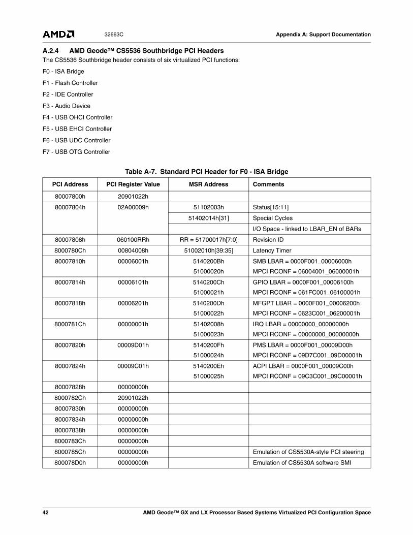
A.2.4 AMD Geode™ CS5536 Southbridge PCI HeadersThe CS5536 Southbridge header consists of six virtualized PCI functions:
F0 - ISA Bridge
F1 - Flash Controller
F2 - IDE Controller
F3 - Audio Device
F4 - USB OHCI Controller
F5 - USB EHCI Controller
F6 - USB UDC Controller
F7 - USB OTG Controller
Table A-7. Standard PCI Header for F0 - ISA Bridge
PCI Address PCI Register Value MSR Address Comments
80007800h 20901022h
80007804h 02A00009h 51102003h Status[15:11]
51402014h[31] Special Cycles
I/O Space - linked to LBAR_EN of BARs
80007808h 060100RRh RR = 51700017h[7:0] Revision ID
8000780Ch 00804008h 51002010h[39:35] Latency Timer
80007810h 00006001h 5140200Bh
51000020h
SMB LBAR = 0000F001_00006000h
MPCI RCONF = 06004001_06000001h
80007814h 00006101h 5140200Ch
51000021h
GPIO LBAR = 0000F001_00006100h
MPCI RCONF = 061FC001_06100001h
80007818h 00006201h 5140200Dh
51000022h
MFGPT LBAR = 0000F001_00006200h
MPCI RCONF = 0623C001_06200001h
8000781Ch 00000001h 51402008h
51000023h
IRQ LBAR = 00000000_00000000h
MPCI RCONF = 00000000_00000000h
80007820h 00009D01h 5140200Fh
51000024h
PMS LBAR = 0000F001_00009D00h
MPCI RCONF = 09D7C001_09D00001h
80007824h 00009C01h 5140200Eh
51000025h
ACPI LBAR = 0000F001_00009C00h
MPCI RCONF = 09C3C001_09C00001h
80007828h 00000000h
8000782Ch 20901022h
80007830h 00000000h
80007834h 00000000h
80007838h 00000000h
8000783Ch 00000000h
8000785Ch 00000000h Emulation of CS5530A-style PCI steering
800078D0h 00000000h Emulation of CS5530A software SMI
42 AMD Geode™ GX and LX Processor Based Systems Virtualized PCI Configuration Space
Appendix A: Support Documentation 32663C
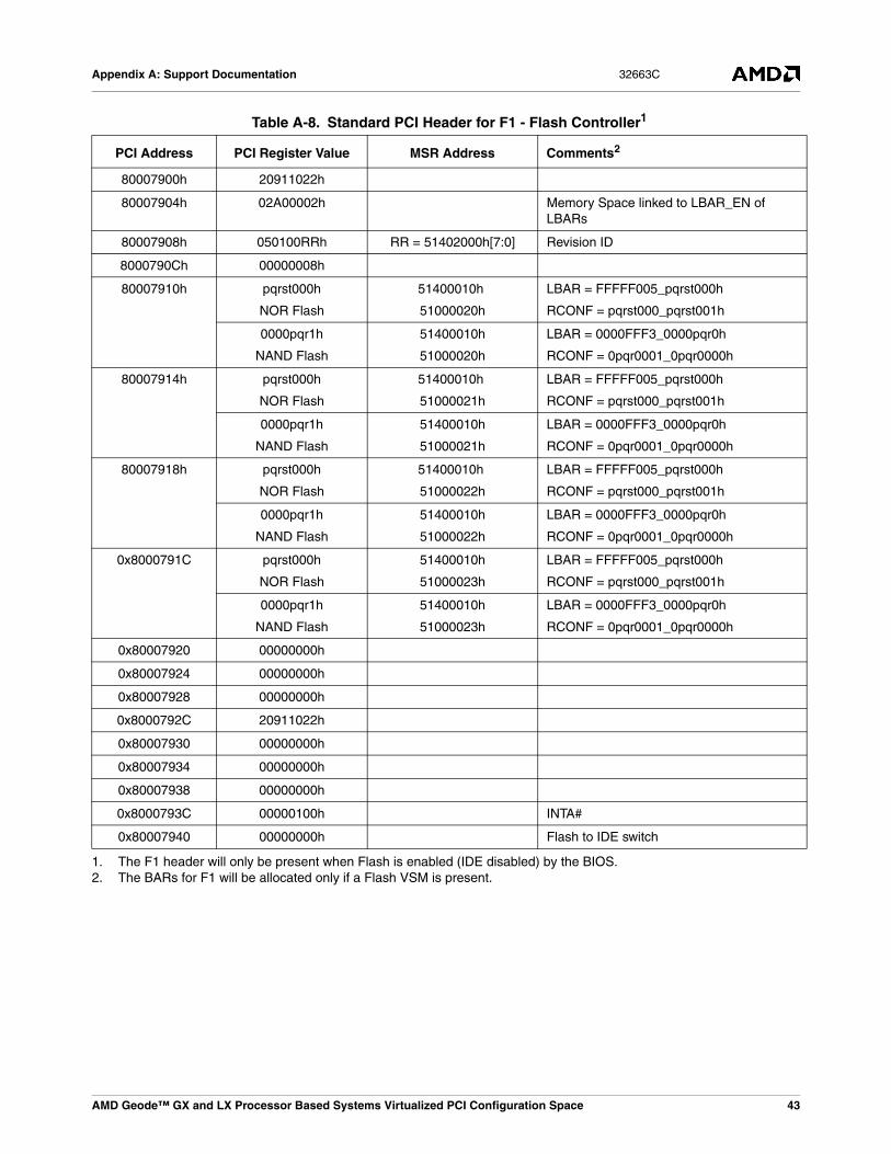
Table A-8. Standard PCI Header for F1 - Flash Controller1
1. The F1 header will only be present when Flash is enabled (IDE disabled) by the BIOS.
PCI Address PCI Register Value MSR Address Comments2
2. The BARs for F1 will be allocated only if a Flash VSM is present.
80007900h 20911022h
80007904h 02A00002h Memory Space linked to LBAR_EN of LBARs
80007908h 050100RRh RR = 51402000h[7:0] Revision ID
8000790Ch 00000008h
80007910h pqrst000h
NOR Flash
51400010h
51000020h
LBAR = FFFFF005_pqrst000h
RCONF = pqrst000_pqrst001h
0000pqr1h
NAND Flash
51400010h
51000020h
LBAR = 0000FFF3_0000pqr0h
RCONF = 0pqr0001_0pqr0000h
80007914h pqrst000h
NOR Flash
51400010h
51000021h
LBAR = FFFFF005_pqrst000h
RCONF = pqrst000_pqrst001h
0000pqr1h
NAND Flash
51400010h
51000021h
LBAR = 0000FFF3_0000pqr0h
RCONF = 0pqr0001_0pqr0000h
80007918h pqrst000h
NOR Flash
51400010h
51000022h
LBAR = FFFFF005_pqrst000h
RCONF = pqrst000_pqrst001h
0000pqr1h
NAND Flash
51400010h
51000022h
LBAR = 0000FFF3_0000pqr0h
RCONF = 0pqr0001_0pqr0000h
0x8000791C pqrst000h
NOR Flash
51400010h
51000023h
LBAR = FFFFF005_pqrst000h
RCONF = pqrst000_pqrst001h
0000pqr1h
NAND Flash
51400010h
51000023h
LBAR = 0000FFF3_0000pqr0h
RCONF = 0pqr0001_0pqr0000h
0x80007920 00000000h
0x80007924 00000000h
0x80007928 00000000h
0x8000792C 20911022h
0x80007930 00000000h
0x80007934 00000000h
0x80007938 00000000h
0x8000793C 00000100h INTA#
0x80007940 00000000h Flash to IDE switch
AMD Geode™ GX and LX Processor Based Systems Virtualized PCI Configuration Space 43
Appendix A: Support Documentation32663C
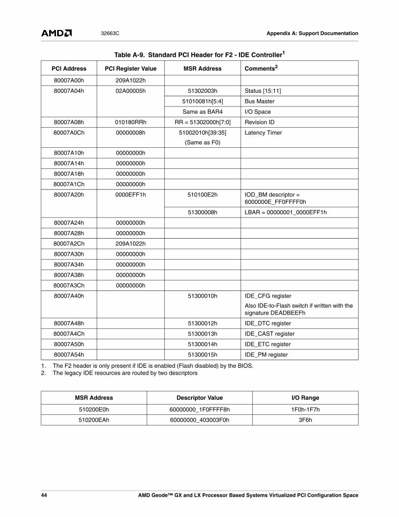
Table A-9. Standard PCI Header for F2 - IDE Controller1
1. The F2 header is only present if IDE is enabled (Flash disabled) by the BIOS.
PCI Address PCI Register Value MSR Address Comments2
2. The legacy IDE resources are routed by two descriptors
80007A00h 209A1022h
80007A04h 02A00005h 51302003h Status [15:11]
51010081h[5:4] Bus Master
Same as BAR4 I/O Space
80007A08h 010180RRh RR = 51302000h[7:0] Revision ID
80007A0Ch 00000008h 51002010h[39:35]
(Same as F0)
Latency Timer
80007A10h 00000000h
80007A14h 00000000h
80007A18h 00000000h
80007A1Ch 00000000h
80007A20h 0000EFF1h 510100E2h IOD_BM descriptor = 6000000E_FF0FFFF0h
51300008h LBAR = 00000001_0000EFF1h
80007A24h 00000000h
80007A28h 00000000h
80007A2Ch 209A1022h
80007A30h 00000000h
80007A34h 00000000h
80007A38h 00000000h
80007A3Ch 00000000h
80007A40h 51300010h IDE_CFG register
Also IDE-to-Flash switch if written with the signature DEADBEEFh
80007A48h 51300012h IDE_DTC register
80007A4Ch 51300013h IDE_CAST register
80007A50h 51300014h IDE_ETC register
80007A54h 51300015h IDE_PM register
MSR Address Descriptor Value I/O Range
510200E0h 60000000_1F0FFFF8h 1F0h-1F7h
510200EAh 60000000_403003F0h 3F6h
44 AMD Geode™ GX and LX Processor Based Systems Virtualized PCI Configuration Space
Appendix A: Support Documentation 32663C
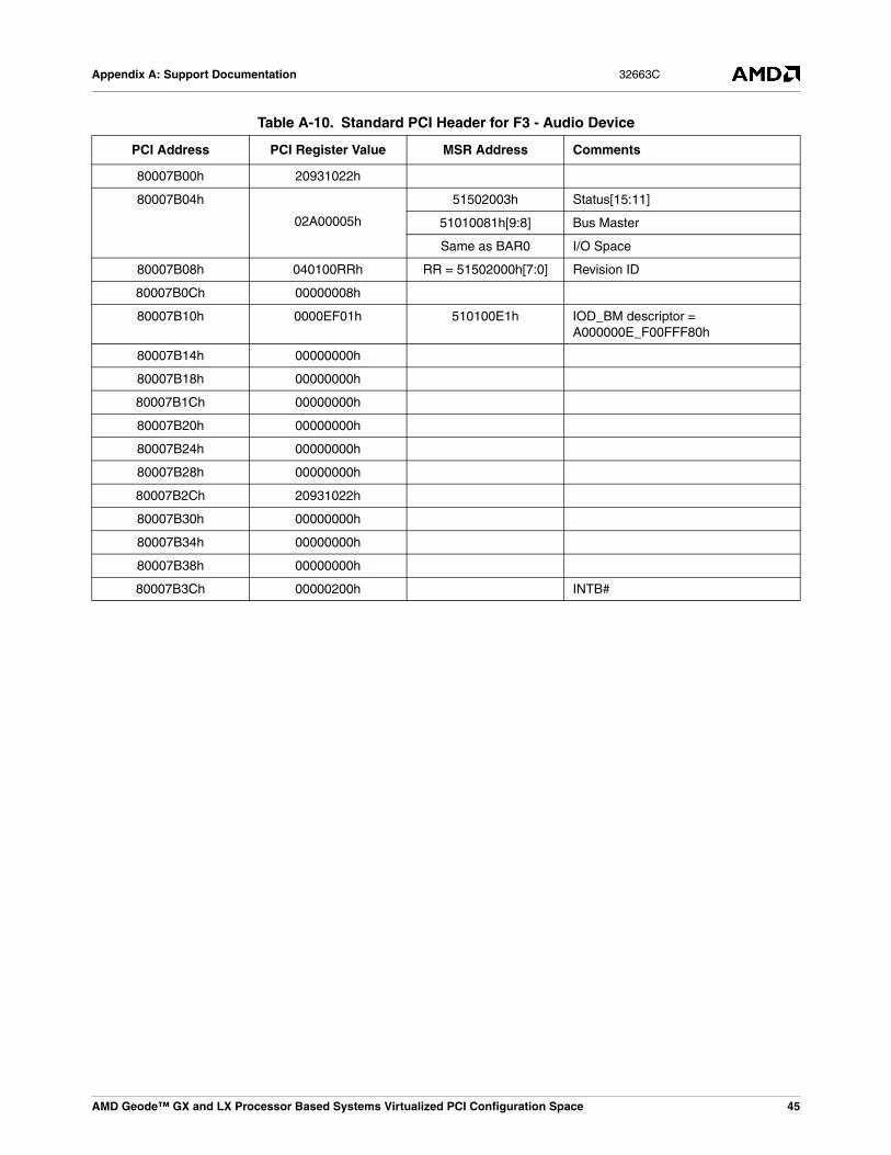
Table A-10. Standard PCI Header for F3 - Audio Device
PCI Address PCI Register Value MSR Address Comments
80007B00h 20931022h
80007B04h
02A00005h
51502003h Status[15:11]
51010081h[9:8] Bus Master
Same as BAR0 I/O Space
80007B08h 040100RRh RR = 51502000h[7:0] Revision ID
80007B0Ch 00000008h
80007B10h 0000EF01h 510100E1h IOD_BM descriptor = A000000E_F00FFF80h
80007B14h 00000000h
80007B18h 00000000h
80007B1Ch 00000000h
80007B20h 00000000h
80007B24h 00000000h
80007B28h 00000000h
80007B2Ch 20931022h
80007B30h 00000000h
80007B34h 00000000h
80007B38h 00000000h
80007B3Ch 00000200h INTB#
AMD Geode™ GX and LX Processor Based Systems Virtualized PCI Configuration Space 45

Appendix A: Support Documentation32663C
Table A-11. Standard PCI Header for F4 - USB OHCI Controller
PCI Address PCI Register Value MSR Address Comments
80007C00h 20941022h
80007C04h 02300006h 51200008h[34] Bus Master
51200008h[33] Memory Enable
80007C08h 0C0310RRh RR = 51200000h[7:0] Revision ID
80007C0Ch 00000008h
80007C10h
EFF00000h
51010023h P2D_BMK = 400000EF_F00FFFFFh
51400009h KEL1 LBAR = FFFFF001_EFF00000h
51200008h[31:0] USBMSROHCB[31:0] = EFF00000h
80007C14h 00000000h
80007C18h 00000000h
80007C1Ch 00000000h
80007C20h 00000000h
80007C24h 00000000h
80007C28h 00000000h
80007C2Ch 20941022h
80007C30h 00000000h
80007C34h 00000040h Capabilities Pointer
80007C38h 00000000h
80007C3Ch 0000040Bh INTD# / IRQ11
80007C40h C8020001h Power Management
80007C44h 00000000h
46 AMD Geode™ GX and LX Processor Based Systems Virtualized PCI Configuration Space

Appendix A: Support Documentation 32663C
Table A-12. Standard PCI Header for F5 - USB EHCI Controller
PCI Address PCI Register Value MSR Address Comments
80007D00h 20951022h
80007D04h 02300006h 51200009h[34] Bus Master
51200009h[33] Memory Enable
80007D08h 0C0320RRh RR = 5120000h0[7:0] Revision ID
80007D0Ch 00000008h
80007D10h EFD00000h 51010024h P2D_BMK = 400000EF_D00FFFFFh
51200009h[31:8] USBMSREHCB[31:0] = EFD00000h
80007D14h 00000000h
80000DC8h 00000000h
80007D1Ch 00000000h
80007D20h 00000000h
80007D24h 00000000h
80007D28h 00000000h
80007D2Ch 20951022h
80007D30h 00000000h
80007D34h 00000040h Capabilities Pointer
80007D38h 00000000h
80007D3Ch 0000040Bh INTD# / IRQ11
80007D40h C8020001h Power Management
80007D44h 00000000h
80007D50h 00000001h 51200009h[53:48] LEGSMIEN
80007D54h 51200009h[53:48] LEGSMIEN
80007D60h 20h SBRN (R/O)
80007D61h 20h 51200009h[45:40] FLADJ (R/W)
AMD Geode™ GX and LX Processor Based Systems Virtualized PCI Configuration Space 47
Appendix A: Support Documentation32663C
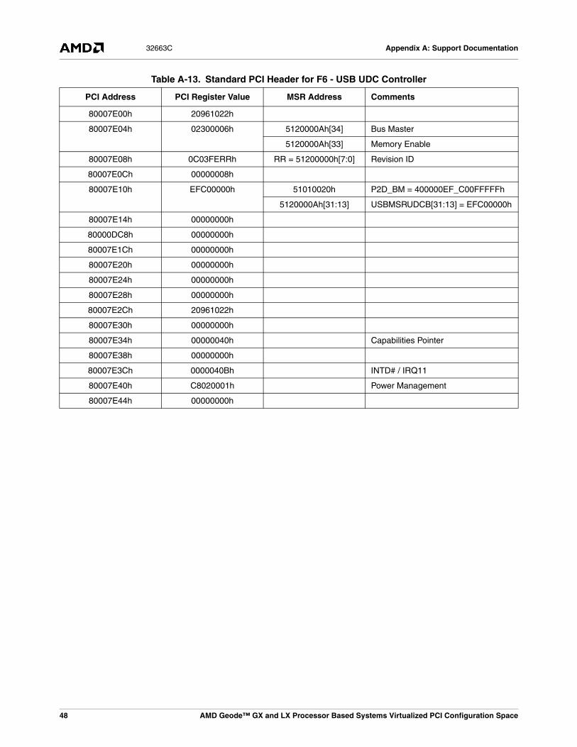
Table A-13. Standard PCI Header for F6 - USB UDC Controller
PCI Address PCI Register Value MSR Address Comments
80007E00h 20961022h
80007E04h 02300006h 5120000Ah[34] Bus Master
5120000Ah[33] Memory Enable
80007E08h 0C03FERRh RR = 51200000h[7:0] Revision ID
80007E0Ch 00000008h
80007E10h EFC00000h 51010020h P2D_BM = 400000EF_C00FFFFFh
5120000Ah[31:13] USBMSRUDCB[31:13] = EFC00000h
80007E14h 00000000h
80000DC8h 00000000h
80007E1Ch 00000000h
80007E20h 00000000h
80007E24h 00000000h
80007E28h 00000000h
80007E2Ch 20961022h
80007E30h 00000000h
80007E34h 00000040h Capabilities Pointer
80007E38h 00000000h
80007E3Ch 0000040Bh INTD# / IRQ11
80007E40h C8020001h Power Management
80007E44h 00000000h
48 AMD Geode™ GX and LX Processor Based Systems Virtualized PCI Configuration Space

Appendix A: Support Documentation 32663C
Table A-14. Standard PCI Header for F7 - USB OTG Controller
PCI Address PCI Register Value MSR Address Comments
80007F00h 20971022h
80007F04h 02300002h 5120000Bh[33] Memory Enable
80007F08h 0C0380RRh RR = 51200000h[7:0] Revision ID
80007F0Ch 00000008h
80007F10h EFB00000h 51010021h P2D_BM = 400000EF_B00FFFFFh
5120000Bh[31:8] USBMSRUOCB [31:8] = EFB00000h
80007F14h 00000000h
80000FC8h 00000000h
80007F1Ch 00000000h
80007F20h 00000000h
80007F24h 00000000h
80007F28h 00000000h
80007F2Ch 20971022h
80007F30h 00000000h
80007F34h 00000040h Capabilities Pointer
80007F38h 00000000h
80007F3Ch 0000040Bh INTD# / IRQ11
80007F40h C8020001h Power Management
80007F44h 00000000h
AMD Geode™ GX and LX Processor Based Systems Virtualized PCI Configuration Space 49

Appendix A: Support Documentation32663C
A.3 Revision HistoryThis is a report of the revision/creation process of the AMD Geode™ GX and LX Processor Based Systems Virtualized PCIConfiguration Space document. Revisions (i.e., additions, deletions, parameter corrections, etc.) are recorded in the tablebelow.
Table A-15. Revision History
Revision # (PDF Date) Revisions / Comments
A (March 2005) Initial release.
B (June 2006) Corrected MSR Addresses in Table A-2 on page 34 for PCI Address 80007914, 80007918, and 8000791C.
Added Standard PCI Header information for F0 and F1, and Table A-9 on page 44 is for the Standard PCI Header for F2 - IDE Controller - was incorrectly labeled as F0 - ISA Bridge.
C (November 2006) Removed confidential for public distribution.
Removed trademark symbol from Virtual System Architecture in Section 1.2 "Background" on page 9 (as it is no longer listed as a recognized AMD trademark). Also removed from Trademark Attribution on page 2.
Changed all references of “Geode” to “AMD Geode”.
Updated Section 3.14 "Capabilities Pointer" on page 23. Capabilities structure has been implemented.
Removed “MSR Access” chapter.
50 AMD Geode™ GX and LX Processor Based Systems Virtualized PCI Configuration Space

Appendix A: Support Documentation 32663C
AMD Geode™ GX and LX Processor Based Systems Virtualized PCI Configuration Space 51

One AMD Place • P.O. Box 3453 • Sunnyvale, CA 94088-3453 USA • Tel: 408-749-4000 or 800-538-8450 • TWX: 910-339-9280 • TELEX: 34-6306
www.amd.com