amd geode™ nx processors data booksupport.amd.com/techdocs/31177h_nx_databook.pdf · nx processor...
TRANSCRIPT
AMD Geode™ NX ProcessorsData Book
April 2006Publication ID: 31177H
AMD Geode™ NX Processors Data Book
2 AMD Geode™ NX Processors Data Book
© 2006 Advanced Micro Devices, Inc. All rights reserved.The contents of this document are provided in connection with Advanced MicroDevices, Inc. (“AMD”) products. AMD makes no representations or warranties withrespect to the accuracy or completeness of the contents of this publication andreserves the right to make changes to specifications and product descriptions atany time without notice. No license, whether express, implied, arising by estoppelor otherwise, to any intellectual property rights is granted by this publication.Except as set forth in AMD’s Standard Terms and Conditions of Sale, AMDassumes no liability whatsoever, and disclaims any express or implied warranty,relating to its products including, but not limited to, the implied warranty of mer-chantability, fitness for a particular purpose, or infringement of any intellectualproperty right.
AMD’s products are not designed, intended, authorized or warranted for use ascomponents in systems intended for surgical implant into the body, or in otherapplications intended to support or sustain life, or in any other application in whichthe failure of AMD’s product could create a situation where personal injury, death,or severe property or environmental damage may occur. AMD reserves the right todiscontinue or make changes to its products at any time without notice.
Trademarks
AMD, the AMD Arrow logo, AMD Athlon, AMD Duron, and combinations thereof, Geode, AMD PowerNow!, and 3DNow! are trademarks of Advanced Micro Devices, Inc.
HyperTransport is a licensed trademark of the HyperTransport Technology Consortium.
MMX is a registered trademark of Intel Corporation in the U.S. and/or other jurisdictions.
Microsoft and Windows are registered trademarks of Microsoft Corporation in the United States and/or other jurisdictions.
Other product names used in this publication are for identification purposes only and may be trademarks of their respective companies.

Contents 31177H
Contents
List of Figures . . . . . . . . . . . . . . . . . . . . . . . . . . . . . . . . . . . . . . . . . . . . . . . . . . . . . . . . . . 5
List of Tables . . . . . . . . . . . . . . . . . . . . . . . . . . . . . . . . . . . . . . . . . . . . . . . . . . . . . . . . . . . 7
1.0 Overview . . . . . . . . . . . . . . . . . . . . . . . . . . . . . . . . . . . . . . . . . . . . . . . . . . . . . . . . . . 91.1 General Description . . . . . . . . . . . . . . . . . . . . . . . . . . . . . . . . . . . . . . . . . . . . . . . . . . . . . . . . . . . 91.2 Microarchitecture Summary . . . . . . . . . . . . . . . . . . . . . . . . . . . . . . . . . . . . . . . . . . . . . . . . . . . . 101.3 Special Features and Requirements . . . . . . . . . . . . . . . . . . . . . . . . . . . . . . . . . . . . . . . . . . . . . 11
2.0 Signal Definitions . . . . . . . . . . . . . . . . . . . . . . . . . . . . . . . . . . . . . . . . . . . . . . . . . . 132.1 Interface Signals Architecture . . . . . . . . . . . . . . . . . . . . . . . . . . . . . . . . . . . . . . . . . . . . . . . . . . 142.2 Pin Assignments . . . . . . . . . . . . . . . . . . . . . . . . . . . . . . . . . . . . . . . . . . . . . . . . . . . . . . . . . . . . 142.3 Signal Descriptions . . . . . . . . . . . . . . . . . . . . . . . . . . . . . . . . . . . . . . . . . . . . . . . . . . . . . . . . . . 25
3.0 Power Management . . . . . . . . . . . . . . . . . . . . . . . . . . . . . . . . . . . . . . . . . . . . . . . . 333.1 Power Management States . . . . . . . . . . . . . . . . . . . . . . . . . . . . . . . . . . . . . . . . . . . . . . . . . . . . 333.2 Connect and Disconnect Protocol . . . . . . . . . . . . . . . . . . . . . . . . . . . . . . . . . . . . . . . . . . . . . . . 383.3 Clock Control . . . . . . . . . . . . . . . . . . . . . . . . . . . . . . . . . . . . . . . . . . . . . . . . . . . . . . . . . . . . . . . 423.4 SYSCLK Multipliers . . . . . . . . . . . . . . . . . . . . . . . . . . . . . . . . . . . . . . . . . . . . . . . . . . . . . . . . . . 423.5 Special Cycles . . . . . . . . . . . . . . . . . . . . . . . . . . . . . . . . . . . . . . . . . . . . . . . . . . . . . . . . . . . . . . 44
4.0 CPUID Support . . . . . . . . . . . . . . . . . . . . . . . . . . . . . . . . . . . . . . . . . . . . . . . . . . . . 45
5.0 Electrical Specifications . . . . . . . . . . . . . . . . . . . . . . . . . . . . . . . . . . . . . . . . . . . . 475.1 Electrical Connections . . . . . . . . . . . . . . . . . . . . . . . . . . . . . . . . . . . . . . . . . . . . . . . . . . . . . . . . 475.2 Absolute Maximum Ratings . . . . . . . . . . . . . . . . . . . . . . . . . . . . . . . . . . . . . . . . . . . . . . . . . . . . 475.3 VCCA Electrical Characteristics . . . . . . . . . . . . . . . . . . . . . . . . . . . . . . . . . . . . . . . . . . . . . . . . . 475.4 VCC_CORE Electrical Characteristics . . . . . . . . . . . . . . . . . . . . . . . . . . . . . . . . . . . . . . . . . . . . . 485.5 DC Characteristics . . . . . . . . . . . . . . . . . . . . . . . . . . . . . . . . . . . . . . . . . . . . . . . . . . . . . . . . . . . 505.6 AC Characteristics . . . . . . . . . . . . . . . . . . . . . . . . . . . . . . . . . . . . . . . . . . . . . . . . . . . . . . . . . . . 555.7 Open-Drain Test Circuit . . . . . . . . . . . . . . . . . . . . . . . . . . . . . . . . . . . . . . . . . . . . . . . . . . . . . . . 585.8 FID_Change Induced PLL Lock Time . . . . . . . . . . . . . . . . . . . . . . . . . . . . . . . . . . . . . . . . . . . . 585.9 Thermal Diode Characteristics . . . . . . . . . . . . . . . . . . . . . . . . . . . . . . . . . . . . . . . . . . . . . . . . . 595.10 Signal and Power-Up Requirements . . . . . . . . . . . . . . . . . . . . . . . . . . . . . . . . . . . . . . . . . . . . . 61
6.0 Mechanical Data . . . . . . . . . . . . . . . . . . . . . . . . . . . . . . . . . . . . . . . . . . . . . . . . . . . 636.1 Die Loading . . . . . . . . . . . . . . . . . . . . . . . . . . . . . . . . . . . . . . . . . . . . . . . . . . . . . . . . . . . . . . . . 636.2 OPGA Package Descriptions . . . . . . . . . . . . . . . . . . . . . . . . . . . . . . . . . . . . . . . . . . . . . . . . . . . 63
7.0 Ordering Information . . . . . . . . . . . . . . . . . . . . . . . . . . . . . . . . . . . . . . . . . . . . . . . 65
AMD Geode™ NX Processors Data Book 3

Contents31177H
Appendix A Supporting Documentation . . . . . . . . . . . . . . . . . . . . . . . . . . . . . . . . . . 67A.1 Thermal Diode Calculations . . . . . . . . . . . . . . . . . . . . . . . . . . . . . . . . . . . . . . . . . . . . . . . . . . . 67A.2 Conventions, Abbreviations, and References . . . . . . . . . . . . . . . . . . . . . . . . . . . . . . . . . . . . . . 69A.3 Revision History . . . . . . . . . . . . . . . . . . . . . . . . . . . . . . . . . . . . . . . . . . . . . . . . . . . . . . . . . . . . 71
4 AMD Geode™ NX Processors Data Book

List of Figures 31177H
List of Figures
Figure 1-1. Typical System Block Diagram . . . . . . . . . . . . . . . . . . . . . . . . . . . . . . . . . . . . . . . . . . . . . . . . 9Figure 2-1. Logic Symbol Diagram . . . . . . . . . . . . . . . . . . . . . . . . . . . . . . . . . . . . . . . . . . . . . . . . . . . . . . 13Figure 2-2. Processor Pin Diagram—Topside View . . . . . . . . . . . . . . . . . . . . . . . . . . . . . . . . . . . . . . . . 15Figure 2-3. Processor Pin Diagram—Bottomside View . . . . . . . . . . . . . . . . . . . . . . . . . . . . . . . . . . . . . . 16Figure 3-1. Processor Power Management States . . . . . . . . . . . . . . . . . . . . . . . . . . . . . . . . . . . . . . . . . 33Figure 3-2. SOFTVID Transition During the AMD Processor System Bus Disconnect for FID_Change . 37Figure 3-3. AMD Processor System Bus Disconnect Sequence in the Stop Grant State . . . . . . . . . . . . 38Figure 3-4. Exiting the Stop Grant State and Bus Connect Sequence . . . . . . . . . . . . . . . . . . . . . . . . . . . 39Figure 3-5. Northbridge Connect State Diagram . . . . . . . . . . . . . . . . . . . . . . . . . . . . . . . . . . . . . . . . . . . 40Figure 3-6. Processor Connect State Diagram . . . . . . . . . . . . . . . . . . . . . . . . . . . . . . . . . . . . . . . . . . . . 41Figure 5-1. VCC_CORE Voltage Waveform . . . . . . . . . . . . . . . . . . . . . . . . . . . . . . . . . . . . . . . . . . . . . . . . 48Figure 5-2. SYSCLK and SYSCLK# Differential Clock Signals . . . . . . . . . . . . . . . . . . . . . . . . . . . . . . . . 50Figure 5-3. SYSCLK Waveform . . . . . . . . . . . . . . . . . . . . . . . . . . . . . . . . . . . . . . . . . . . . . . . . . . . . . . . . 55Figure 5-4. General ATE Open-Drain Test Circuit . . . . . . . . . . . . . . . . . . . . . . . . . . . . . . . . . . . . . . . . . . 58Figure 5-5. Signal Relationship Requirements During Power-Up Sequence . . . . . . . . . . . . . . . . . . . . . . 61Figure 6-1. 28104 OPGA Package Outline . . . . . . . . . . . . . . . . . . . . . . . . . . . . . . . . . . . . . . . . . . . . . . . 64Figure 7-1. OPN for the AMD Geode™ NX Processors . . . . . . . . . . . . . . . . . . . . . . . . . . . . . . . . . . . . . . 65
AMD Geode™ NX Processors Data Book 5

List of Figures31177H
6 AMD Geode™ NX Processors Data Book
List of Tables 31177H
List of Tables
Table 2-1. Pin Assignment - Sorted by Pin Number . . . . . . . . . . . . . . . . . . . . . . . . . . . . . . . . . . . . . . . . 17Table 2-2. Pin Assignment - Sorted Alphabetically by Signal Name . . . . . . . . . . . . . . . . . . . . . . . . . . . 23Table 2-3. SOFTVID[4:0] and VID[4:0] Code to Voltage Definition . . . . . . . . . . . . . . . . . . . . . . . . . . . . . 30Table 3-1. FID[4:0] SYSCLK Multiplier Combinations () . . . . . . . . . . . . . . . . . . . . . . . . . . . . . . . . . . . . . 43Table 3-2. Processor Special Cycle Definition . . . . . . . . . . . . . . . . . . . . . . . . . . . . . . . . . . . . . . . . . . . . 44Table 5-1. Absolute Ratings . . . . . . . . . . . . . . . . . . . . . . . . . . . . . . . . . . . . . . . . . . . . . . . . . . . . . . . . . . 47Table 5-2. VCCA Electrical Characteristics . . . . . . . . . . . . . . . . . . . . . . . . . . . . . . . . . . . . . . . . . . . . . . . 47Table 5-3. VCC_CORE Electrical Characteristics . . . . . . . . . . . . . . . . . . . . . . . . . . . . . . . . . . . . . . . . . . . 48Table 5-4. Voltage and Frequency Combinations . . . . . . . . . . . . . . . . . . . . . . . . . . . . . . . . . . . . . . . . . . 49Table 5-5. SYSCLK and SYSCLK# DC Characteristics () . . . . . . . . . . . . . . . . . . . . . . . . . . . . . . . . . . . 50Table 5-6. SOFTVID[4:0] and VID[4:0] DC Characteristics . . . . . . . . . . . . . . . . . . . . . . . . . . . . . . . . . . 51Table 5-7. FID[3:0] DC Characteristics . . . . . . . . . . . . . . . . . . . . . . . . . . . . . . . . . . . . . . . . . . . . . . . . . . 51Table 5-8. PICD[1:0]# and PICCLK (APIC Pins) DC Characteristics . . . . . . . . . . . . . . . . . . . . . . . . . . . 52Table 5-9. AMD Processor System Bus DC Characteristics . . . . . . . . . . . . . . . . . . . . . . . . . . . . . . . . . . 53Table 5-10. General DC Characteristics . . . . . . . . . . . . . . . . . . . . . . . . . . . . . . . . . . . . . . . . . . . . . . . . . . 54Table 5-11. SYSCLK and SYSCLK# AC Characteristics . . . . . . . . . . . . . . . . . . . . . . . . . . . . . . . . . . . . . 55Table 5-12. PICD[1:0]# and PICCLK (APIC Pins) AC Characteristics . . . . . . . . . . . . . . . . . . . . . . . . . . . 56Table 5-13. AMD Processor System Bus AC Characteristics . . . . . . . . . . . . . . . . . . . . . . . . . . . . . . . . . . 56Table 5-14. General AC Characteristics . . . . . . . . . . . . . . . . . . . . . . . . . . . . . . . . . . . . . . . . . . . . . . . . . . 57Table 5-15. FID_Change Induced PLL Lock Time . . . . . . . . . . . . . . . . . . . . . . . . . . . . . . . . . . . . . . . . . . 58Table 5-16. Thermal Diode Electrical Characteristics . . . . . . . . . . . . . . . . . . . . . . . . . . . . . . . . . . . . . . . . 59Table 5-17. Guidelines for Platform Thermal Protection of the Processor . . . . . . . . . . . . . . . . . . . . . . . . 59Table 5-18. Thermal Power Performance Specifications . . . . . . . . . . . . . . . . . . . . . . . . . . . . . . . . . . . . . 60Table 6-1. Mechanical Loading . . . . . . . . . . . . . . . . . . . . . . . . . . . . . . . . . . . . . . . . . . . . . . . . . . . . . . . . 63Table 6-2. 28104 OPGA Package Dimensions . . . . . . . . . . . . . . . . . . . . . . . . . . . . . . . . . . . . . . . . . . . . 63Table 7-1. Valid OPN Combinations . . . . . . . . . . . . . . . . . . . . . . . . . . . . . . . . . . . . . . . . . . . . . . . . . . . . 65Table A-1. Constants and Variables for the Ideal Diode Equation . . . . . . . . . . . . . . . . . . . . . . . . . . . . . 67Table A-2. Temperature Offset Equation Constants and Variables . . . . . . . . . . . . . . . . . . . . . . . . . . . . 67Table A-3. Definitions of Abbreviations . . . . . . . . . . . . . . . . . . . . . . . . . . . . . . . . . . . . . . . . . . . . . . . . . . 69Table A-4. Definitions of Acronyms . . . . . . . . . . . . . . . . . . . . . . . . . . . . . . . . . . . . . . . . . . . . . . . . . . . . 70Table A-5. Revision History . . . . . . . . . . . . . . . . . . . . . . . . . . . . . . . . . . . . . . . . . . . . . . . . . . . . . . . . . . . 71
AMD Geode™ NX Processors Data Book 7

List of Tables31177H
8 AMD Geode™ NX Processors Data Book
AMD Geode™ NX Processors Data
Overview 31177H
*The AMD Geode™ NX 1750@14W procesat 667 MHz. Model numbers reflect perform
11.0Overview
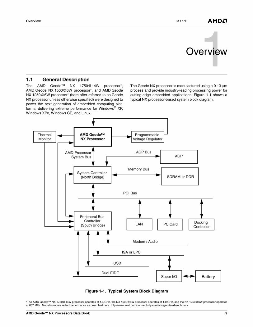
1.1 General DescriptionThe AMD Geode™ NX 1750@14W processor*,AMD Geode NX 1500@6W processor*, and AMD GeodeNX 1250@6W processor* (here after referred to as GeodeNX processor unless otherwise specified) were designed topower the next generation of embedded computing plat-forms, delivering extreme performance for Windows® XP,Windows XPe, Windows CE, and Linux.
The Geode NX processor is manufactured using a 0.13 μmprocess and provide industry-leading processing power forcutting-edge embedded applications. Figure 1-1 shows atypical NX processor-based system block diagram.
Figure 1-1. Typical System Block Diagram
SDRAM or DDR
Memory Bus
AGP
PCI Bus
LAN PC Card
ISA or LPC
USB
Dual EIDE
Modem / Audio
Battery
AGP Bus
Thermal AMD Geode™ NX Processor
Programmable Voltage RegulatorMonitor
AMD ProcessorSystem Bus
System Controller (North Bridge)
Peripheral Bus Controller
(South Bridge)Docking Controller
Super I/O
Book 9
sor operates at 1.4 GHz, the NX 1500@6W processor operates at 1.0 GHz, and the NX 1250@6W processor operatesance as described here: http://www.amd.com/connectivitysolutions/geodenxbenchmark.
Overview31177H
The Geode NX processor implements AMD PowerNow!™technology, which achieves lower power states by adjustingthe processor’s voltage and/or frequency. TheNX 1500@6W* and NX 1250@6W* use fixed operatingvoltages, and are therefore only able to achieve lowerpower by adjusting the processor’s frequency, while theNX 1750@14W* can be adjusted in frequency and voltagefor lower power operation. See Section 5.4.1 "Valid Voltageand Frequency Combinations" on page 49 for more infor-mation. The Geode NX processor is available in a low-pro-file, lidless organic pin grid array (OPGA) package.
The Geode NX processor features seventh-generationmicroarchitecture with integrated L2 cache that supportsthe growing processor and system bandwidth requirementsof emerging software, graphics, I/O, and memory technolo-gies. The high-speed execution core in the processorincludes multiple x86 instruction decoders, a dual-ported128 KB split level-one (L1) cache (made up of a 64 KB L1instruction cache and a 64 KB L1 data cache), a 256 KB L2integrated cache, three independent integer pipelines,three address calculation pipelines, and a fully pipelined,out-of-order, floating-point engine.
The processor’s microarchitecture supports AMD3DNow!™ Professional technology, a high-performancecache architecture, and the 266 MHz, 2.1 GB per secondAMD processor system bus. The AMD processor systembus is designed to combine the latest technologicaladvances, such as point-to-point topology, source-synchro-nous packet-based transfers, and low-voltage signaling, toprovide an extremely powerful, scalable bus available forany x86 processor. The AMD processor system bus oper-ates at twice the front side bus (FSB) frequency.
The Geode NX processor is binary-compatible with existingx86 software and backwards compatible with applicationsoptimized for enhanced 3DNow!, MMX®, and SSE instruc-tions. Using a data format and single-instruction multiple-data (SIMD) operations based on the MMX instructionmodel, the Geode NX processor can produce as many asfour, 32-bit, single-precision floating-point results per clockcycle. The implemented 3DNow! Professional technologyincludes new integer multimedia instructions and soft-ware-directed data movement instructions for optimizingsuch applications as streaming video for the Internet, aswell as new instructions for digital signal processing (DSP)and communications applications.
1.2 Microarchitecture SummaryThe following features summarize the Geode NX proces-sor’s microarchitecture:
■ Advanced 0.13 μm technology for higher frequency scaling and lower power consumption
■ 128 KB L1 cache (made up of a 64 KB L1 instruction cache and a 64 KB L1 data cache)
■ 256 KB L2 cache with hardware data prefetch
■ Pipelined floating-point execution unit that executes a peak of three x87 instructions per clock cycle
■ Support for MMX, SSE, and 3DNow! Professional instruction sets for high-performance multimedia instruc-tion processing
■ Dynamic transitions between higher performance and lower power processor performance states are supported by AMD PowerNow! software and the Windows® XP operating system
■ ACPI 1.0b and ACPI 2.0 compliant power management
■ Three out-of-order, superscalar, pipelined integer units
■ Three out-of-order, superscalar, pipelined address calculation units
■ A 266 MHz AMD processor system bus enabling leading-edge system bandwidth for data move-ment-intensive applications
10 AMD Geode™ NX Processors Data Book
*The AMD Geode™ NX 1750@14W processor operates at 1.4 GHz, the NX 1500@6W processor operates at 1.0 GHz, and the NX 1250@6W processor operatesat 667 MHz. Model numbers reflect performance as described here: http://www.amd.com/connectivitysolutions/geodenxbenchmark.
Overview 31177H
1.3 Special Features and RequirementsThis data book provides the electrical, thermal andmechanical specifications for the AMD Geode NX proces-sor in the OPGA package. System builders have threechoices when determining the optimal solution for theirdesign needs:
• AMD Geode™ NX 1250@6W processor* for value embedded applications requiring fanless performance.
• AMD Geode™ NX 1500@6W processor* for fanless, high performance (up to 1GHz) with very low power consumption designs.
• AMD Geode™ NX 1750@14W processor*, highest performance for demanding graphics, multimedia and high horsepower applications.
The Geode NX processor has some very important opera-tional conditions that the board designer must take intoaccount. They include:
• A tighter processor core voltage tolerance is required for all negative excursions. A total tolerance of –50 mV is required for the voltage delivered to the core of all versions of this processor. This DC tolerance is inclusive of any AC transients that may occur due to changing processor current requirements. See Figure 5-1 "VCC_CORE Voltage Waveform" on page 48 for a graph-ical representation of this tolerance. Proper output filter component layout is critical to achieving this tolerance at the higher loading of these processors.
• The Geode NX processor has a 133 MHz FSB. By using both edges of the FSB clock, the processor is able to achieve a maximum of 266 million transfers per second (MTPS) per data line for the AMD processor system bus. The increased speed of the FSB at low voltage places additional design constraints on the implementation of the AMD processor system bus. Refer to the AMD Athlon™ Processor-Based Motherboard Design Guide (publication ID 24363) and the AMD Geode™ NX Processors Addendum to AMD Athlon™ Processor-Based Motherboard Design Guide (publication ID 31860) for additional information on circuitry and layout guidelines required to fully support this processor.
• The Geode NX processor supports the following ranges:
— The operational voltage for the NX 1250@6W processor* is fixed at 1.1V.
— The operational voltage for the NX 1500@6W processor* is fixed at 1.0V.
— The operational voltage range for the NX 1750@14W processor* is from 1.05V to 1.25V. Specific imple-mentations may choose not to utilize the entire range due to other operational constraints.
• The Geode NX processor has a 6x start-up multiplier.
• The Geode NX processor is compatible with processor system boards that implement an FSB detect circuit. Refer to the AMD Athlon™ Processor-Based Mother-board Design Guide (publication ID 24363) and AMD Geode™ NX Processors Addendum to AMD Athlon™ Processor-Based Motherboard Design Guide (publica-tion ID 31860) for implementation details.
dIdt-----
AMD Geode™ NX Processors Data Book 11
*The AMD Geode™ NX 1750@14W processor operates at 1.4 GHz, the NX 1500@6W processor operates at 1.0 GHz, and the NX 1250@6W processor operatesat 667 MHz. Model numbers reflect performance as described here: http://www.amd.com/connectivitysolutions/geodenxbenchmark.

Overview31177H
12 AMD Geode™ NX Processors Data Book

AMD Geode™ NX Processors Data
Signal Definitions 31177H
22.0Signal Definitions
Figure 2-1 is a logic symbol diagram for the AMD Geode™ NX processor, showing the logical grouping of the input and out-put signals.
Figure 2-1. Logic Symbol Diagram
SDATA[63:0]#
SDATAINCLK[3:0]#
SDATAOUTCLK[3:0]#Data
SADDIN[14:2]#SADDINCLK#Probe/SysCMD
SADDOUT[14:2]#SADDOUTCLK#
VID[4:0]
FID[3:0]
A20M#
CLKFWDRST
CONNECT
COREFB
COREFB#
FERR IGNNE# INIT# INTR NMI
PROCRDY
PWROK
RESET#
SFILLVALID#
SMI#
STPCLK#
SYSCLK#
Clock
Voltage
Frequency
Legacy
Request
AMD Geode™ NX Processor
SDATAINVALID#
SDATAOUTVALID#
Power
Thermal
Diode
THERMDA
THERMDC
FLUSH#
SOFTVID[4:0]
FSB_SenseFront-Side-Bus
PICCLKPICD[1:0]#
APIC
Autodetect
Control
Control
Management& Initialization
(CLKIN# + RSTCLK#)SYSCLK#
(CLKIN + RSTCLK)
Book 13
Signal Definitions31177H
2.1 Interface Signals ArchitectureThe architecture is designed to deliver excellent datamovement bandwidth for next-generation x86 platforms aswell as the high-performance required by enterprise-classapplication software. The system bus architecture consistsof three high-speed channels (a unidirectional processorrequest channel, a unidirectional probe channel, and a 64-bit bidirectional data channel), source-synchronous clock-ing, and a packet-based protocol. In addition, the systembus supports several control, clock, and legacy signals.The interface signals use an impedance controlledpush-pull, low-voltage, swing-signaling technology con-tained within the Socket A socket.
For more information, see Section 2.1.3 "AMD ProcessorSystem Bus Signals", Section 2.3.4 "AMD Processor Sys-tem Bus Interface Signals" on page 26, and theAMD Athlon™ Processor System Bus Specification (publi-cation ID 21902).
2.1.1 Signaling TechnologyThe AMD processor system bus uses a low-voltage, swing-signaling technology, that has been enhanced to providelarger noise margins, reduced ringing, and variable voltagelevels. The signals are push-pull and impedance compen-sated. The signal inputs use differential receivers thatrequire a reference voltage (VREF). The reference signal isused by the receivers to determine if a signal is asserted orde-asserted by the source. Termination resistors are notneeded because the driver is impedance-matched to thecircuit board and a high impedance reflection is used at thereceiver to bring the signal past the input threshold.
For more information about signals, see Section 2.3 "Sig-nal Descriptions" on page 25.
2.1.2 Push-Pull (PP) DriversThe AMD Geode NX processors support push-pull (PP)drivers. The system logic configures the processor with theconfiguration parameter called SysPushPull (1 = PP). Theimpedance of the PP drivers is set to match the impedanceof the circuit board by two external resistors connected tothe ZN and ZP pins.
See Section 2.3.12 "Power, Ground and CompensationCircuit Connections" on page 31 for more information.
2.1.3 AMD Processor System Bus SignalsThe AMD processor system bus is a clock-forwarded,point-to-point interface with the following threepoint-to-point channels:
• A 13-bit unidirectional output address/command channel
• A 13-bit unidirectional input address/command channel
• A 72-bit bidirectional data channel
For more information, see Section 5.0 "Electrical Specifica-tions" on page 47 and the AMD Athlon™ Processor Sys-tem Bus Specification (publication ID 21902).
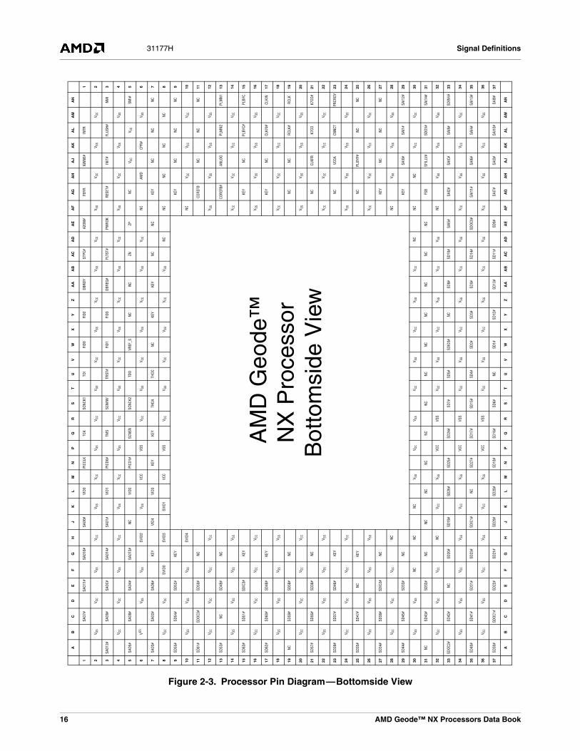
2.2 Pin AssignmentsThis subsection defines the pin assignments:
• Figure 2-2 on page 15 and Figure 2-3 on page 16 shows the Organic Pin Grid Array (OPGA) for the Geode NX processor, top and bottom views respectively. Because some of the pin names are too long to fit in the grid, they are abbreviated.
• Table 2-1 on page 17 lists all the pins sorted by pin number along with the abbreviation (where necessary) and some additional pin information.
• Table 2-2 on page 23 is a quick reference and sorts the pins alphabetically by signal name (full name; no abbre-viation or other parameters are called out) with the corresponding pin number.
PGA Orientation PinsNo pin is present at pin locations A1 and AN1. Circuitboard designers should not allow for a PGA socket pin atthese locations.
For more information, see the AMD Athlon™ Processor-Based Motherboard Design Guide (publication ID 24363)and AMD Geode™ NX Processors Addendum toAMD Athlon™ Processor-Based Motherboard DesignGuide (publication ID 31860).
14 AMD Geode™ NX Processors Data Book

Signal Definitions 31177H
Figure 2-2. Processor Pin Diagram—Topside View
12
34
56
78
910
1112
1314
1516
1718
1920
2122
2324
2526
2728
29
3031
3233
3435
3637
ASA
O12
#SA
O5#
SAO
3#SD
55#
SD61
#SD
53#
SD63
#SD
62#
NC
SD57
#SD
39#
SD35
#SD
34#
SD44
#N
CSD
OC2#
SD40
#SD
30#
A
BV S
SV C
CV S
SV C
CV S
SV C
CV S
SV C
CV S
SV C
CV S
SV C
CV S
SV C
CV S
SV C
CV S
SV C
CB
CSA
O7#
SAO
9#SA
O8#
SAO
2#SD
54#
SDO
C3#
NCSD
51#
SD60
#SD
59#
SD56
#SD
37#
SD47
#SD
38#
SD45
#SD
43#
SD42
#SD
#41
SDOC
1#C
DV C
CV C
CV S
SV C
CV S
SV C
CV S
SV C
CVS
SVC
CV S
SV C
CV S
SVC
CV S
SV C
CV S
SV S
SD
ESA
O11
#SA
OC#
SAO
4#SA
O6#
SD52
#SD
50#
SD#4
9SD
IC#3
SD#4
8SD
#58
SD#3
6SD
#46
NC
SDIC
#2SD
33#
SD32
#N
CSD
31#
SD22
#E
FV S
SV S
SV S
SSV
ID0
V SS
V CC
V SS
V CC
VSS
VCC
V SS
V CC
V SS
V CC
NCV C
CV C
CV C
CF
GSA
O10
#SA
O14
#SA
O13
#KE
YKE
YN
CNC
G15
KEY
NC
NCKE
Y KE
YNC
NC
NC
SD#2
0SD
#23
SD#2
1G
HV C
CV C
CSV
ID2
SVID
3SV
ID4
V CC
V SS
V CC
V SS
V CC
V SS
V CC
V SS
NC
NCN
CV S
SV S
SH
JSA
O0#
SAO
1#N
CVI
D4
AM
D G
eode
™N
X P
roce
ssor
Tops
ide
Vie
w
NC
SD19
#SD
IC1#
SD29
#J
KV S
SV S
SV S
SSV
ID1
NCV C
CV C
CV C
CK
LVI
D0
VID
1VI
D2VI
D3
NC
SD26
#N
CSD
28#
L
MV C
CV C
CV C
CV C
CV S
SV S
SV S
SV S
SM
NPI
CCLK
PICD
0#PI
CD1#
KEY
NC
SD25
#SD
27#
SD18
#N
PV S
SV S
SV S
SV S
SV C
CV C
CV C
CV C
CP
QTC
KTM
SSC
NSN
KEY
NC
SD24
#SD
17#
SD16
#Q
RV C
CV C
CV C
CV C
CV S
SV S
SV S
SV S
SR
SSC
NCK1
SCN
INV
SCNC
K2TH
DA
NC
SD7#
SD15
#SD
6#S
TV S
SV S
SV S
SV S
SV C
CV C
CV C
CV C
CT
UTD
ITR
ST#
TDO
THD
CN
CSD
5#SD
4#N
CU
VV C
CV C
CV C
CV C
CV S
SV S
SV S
SV S
SV
WFI
D0FI
D1VR
EF_S
NC
NC
SDIC
#0SD
#2SD
#1W
XV S
SV S
SV S
SV S
SV C
CV C
CV C
CV C
CX
YFI
D2FI
D3N
CKE
YN
CN
CSD
3#SD
12#
Y
ZV C
CV C
CV C
CV C
CV S
SV S
SV S
SV S
SZ
AA
DBR
DY
DBR
EQ#
NC
KEY
NC
SD8#
SD0#
SD13
#A
A
AB
V SS
V SS
V SS
V SS
V CC
V CC
V CC
V CC
AB
AC
STPC
#PL
TST#
ZNN
CN
CSD
10#
SD14
#SD
11#
AC
AD
V CC
V CC
V CC
NC
NCV S
SV S
SV S
SA
D
AE
A20M
#PW
ROK
ZPN
CN
CSA
I5#
SDOC
0#SD
9#A
E
AF
V SS
V SS
NC
NC
NC
V SS
V CC
V SS
V CC
V SS
V CC
V SS
V CC
NC
NCN
CV C
CV C
CA
F
AG
FER
RR
ESET
#N
CKE
Y K
EYCO
REF
BCO
REF
B#KE
Y K
EYN
CNC
NC
NC
KEY
KEY
FSB
SAI2
#SA
I11#
SAI7
#A
G
AH
V CC
V CC
AMD
NC
V CC
V SS
V CC
V SS
V CC
V SS
V CC
V SS
V CC
V SS
NCV S
SV S
SV S
SA
H
AJ
IGN
NE#
INIT
#VC
CN
CN
CN
CAN
LOG
NCN
CN
CCL
KFR
V CCA
PLBY
P#NC
SAI0
#SF
ILLV
#SA
IC#
SAI6
#SA
I3#
AJ
AK
V SS
V SS
CPR
#N
CV C
CV S
SV C
CV S
SV C
CV S
SV C
CV S
SV C
CV S
SVC
CV S
SV C
CV C
CA
K
AL
INTR
FLU
SH#
V CC
NC
NC
NC
PLM
N2PL
BYC#
CLKI
N#
RCL
K#K7
COCN
NCT
NC
NCSA
I1#
SDOV
#SA
I8#
SAI4
#SA
I10#
AL
AM
V CC
V SS
V SS
NC
V CC
V SS
V CC
V SS
V CC
V SS
V CC
V SS
V CC
V SS
VCC
V SS
V CC
V SS
AM
AN
NM
ISM
I#N
CN
CN
CPL
MN1
PLBY
CCL
KIN
RCL
KK7
CO#
PRCR
DYN
CNC
SAI1
2#SA
I14#
SDIN
V#SA
I13#
SAI9
#A
N
12
34
56
78
910
1112
1314
1516
1718
1920
2122
2324
2526
2728
2930
3132
3334
3536
37
AMD Geode™ NX Processors Data Book 15
Signal Definitions31177H
Figure 2-3. Processor Pin Diagram—Bottomside View
AB
CD
EF
GH
JK
LM
NP
QR
ST
UV
WX
YZ
AA
AB
AC
AD
AE
AF
AG
AH
AJ
AK
AL
AM
AN
1SA
O7#
SAO
11#
SAO1
0#SA
O0#
VID
0PI
CCLK
TCK
SCN
CK1
TDI
FID
0FI
D2
DBR
DY
STPC
#A2
0M#
FER
RIG
NN
E#IN
TR1
2V S
SV C
CV S
SV C
CV S
SV C
CV S
SV C
CV S
SV C
CV S
SV C
CV S
SV C
CV S
SV C
CV S
SV C
C2
3SA
O12#
SAO
9#SA
OC#
SAO1
4#SA
O1#
VID
1PI
CD0#
TMS
SCN
INV
TRST
#FI
D1
FID
3DB
REQ
#PL
TST#
PWR
OK
RES
ET#
INIT
#FL
USH
#NM
I3
4V C
CV C
CV S
SV C
CV S
SV C
CV S
SV C
CV S
SV C
CV S
SV C
CV S
SV C
CV S
SV C
CV S
SV S
S4
5SA
O5#
SAO
8#SA
O4#
SAO1
3#NC
VID
2PI
CD1#
SCNS
NSC
NCK
2TD
OVR
EF_S
NC
NCZN
ZPNC
V CC
V CC
SMI#
5
6VSS
V SS
V SS
SVID
2V S
SVC
CVS
SV C
CV S
SV C
CV S
SV C
CV S
SV C
CN
CAM
DCP
R#
V SS
6
7SA
O3#
SAO
2#SA
O6#
KEY
VID
4VI
D3
KEY
KEY
THD
ATH
DCN
CKE
YKE
Y N
CN
CKE
YNC
NC
NC
7
8V C
CV C
CSV
ID0
SVID
3SV
ID1
VCC
VSS
V CC
V SS
V CC
V SS
V CC
V SS
NC
NC
NC
NC
NC8
9SD
55#
SD54
#SD
52#
KEY
AM
D G
eode
™N
X P
roce
ssor
Bot
tom
side
Vie
w
KEY
NCN
CN
C9
10V S
SV S
SV S
SSV
ID4
NC
V CC
V CC
V CC
10
11SD
61#
SDOC
3#SD
50#
NC
COR
EFB
NCN
CN
C11
12V C
CV C
CV C
CV C
CV S
SV S
SV S
SV S
S12
13SD
53#
NC
SD49
#N
CCO
REF
B#AN
LOG
PLM
N2
PLM
N1
13
14V S
SV S
SV S
SV S
SV C
CV C
CV C
CV C
C14
15SD
63#
SD51
#SD
IC3#
KEY
KEY
NCPL
BYC#
PLBY
C15
16V C
CV C
CV C
CV C
CV S
SV S
SV S
SV S
S16
17SD
62#
SD60
#SD
48#
KEY
KEY
NCCL
KIN
#CL
KIN
17
18V S
SV S
SV S
SV S
SV C
CV C
CV C
CV C
C18
19N
CSD
59#
SD58
#N
CNC
NCR
CLK#
RCL
K19
20V C
CV C
CV C
CV C
CV S
SV S
SV S
SV S
S20
21SD
57#
SD56
#SD
36#
NC
NCCL
KFR
K7CO
K7CO
#21
22V S
SV S
SV S
SV S
SV C
CV C
CV C
CV C
C22
23SD
39#
SD37
#SD
46#
KEY
NCVC
CACN
NCT
PRCR
DY
23
24V C
CV C
CV C
CV C
CV S
SV S
SV S
SV S
S24
25SD
35#
SD47
#N
CKE
YNC
PLBY
P#N
CN
C25
26V S
SV S
SV S
SV S
SV C
CV C
CV C
CV C
C26
27SD
34#
SD38
#SD
IC2#
NC
KEY
NCN
CN
C27
28V C
CV C
CV C
CNC
NC
V SS
V SS
V SS
28
29SD
44#
SD45
#SD
33#
NC
KEY
SAI0
#SA
I1#
SAI1
2#29
30V S
SV S
SN
CNC
NCV S
SV C
CV S
SV C
CV S
SV C
CV S
SV C
CN
CN
CN
CV C
CV C
C30
31N
CSD
43#
SD32
#N
CNC
NC
NC
NC
NC
NCN
CN
CNC
NC
NC
FSB
SFIL
LV#
SDO
V#SA
I14#
31
32V C
CV C
CV C
CNC
V CC
V SS
VCC
VSS
V CC
V SS
V CC
V SS
V CC
V SS
NC
V SS
V SS
V SS
32
33SD
OC2#
SD42
#N
CSD
20#
SD19
#SD
26#
SD25
#SD
24#
SD7#
SD5#
SDIC
0#N
CSD
8#SD
10#
SAI5
#SA
I2#
SAIC
#SA
I8#
SDIN
V#33
34V S
SV S
SV C
CV S
SV C
CV S
SVC
CVS
SV C
CV S
SV C
CV S
SV C
CV S
SV C
CV S
SV C
CV C
C34
35SD
40#
SD41
#SD
31#
SD23
#SD
IC1#
NC
SD27
#SD
17#
SD15
#SD
4#SD
2#SD
3#SD
0#SD
14#
SDO
C0#
SAI1
1#SA
I6#
SAI4
#SA
I13#
35
36V C
CV S
SV C
CV S
SV C
CV S
SVC
CVS
SV C
CV S
SV C
CV S
SV C
CV S
SV C
CV S
SV C
CV S
S36
37SD
30#
SDOC
1#SD
22#
SD21
#SD
29#
SD28
#SD
18#
SD16
#SD
6#NC
SD1#
SD12
#SD
13#
SD11
#SD
9#SA
I7#
SAI3
#SA
I10#
SAI9
#37
AB
CD
EF
GH
JK
LM
NP
QR
ST
UV
WX
YZ
AA
AB
AC
AD
AE
AF
AG
AH
AJ
AK
AL
AM
AN
16 AMD Geode™ NX Processors Data Book
Signal Definitions 31177H
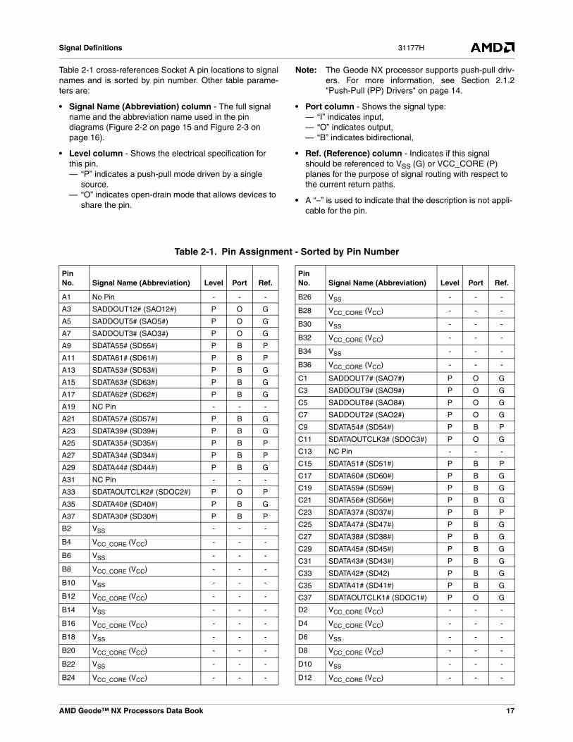
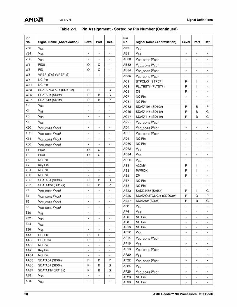
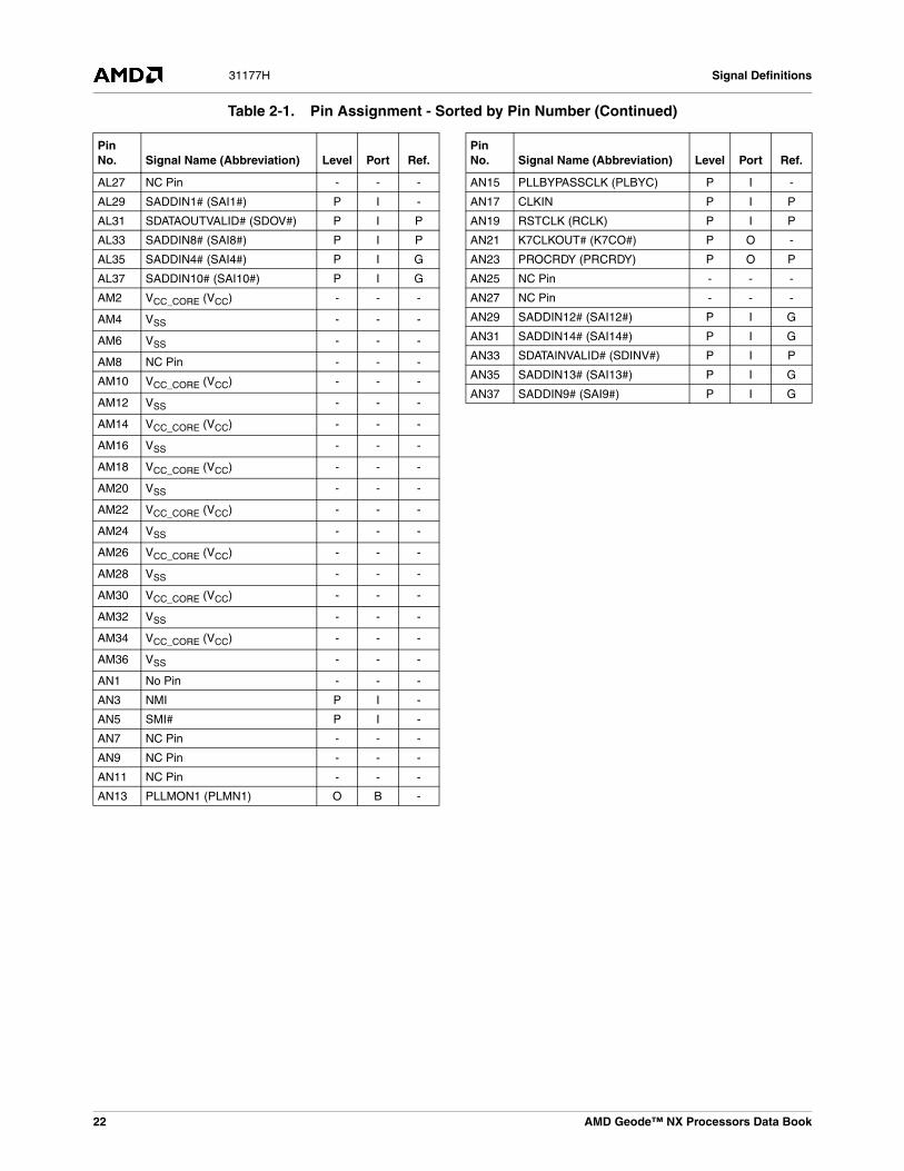
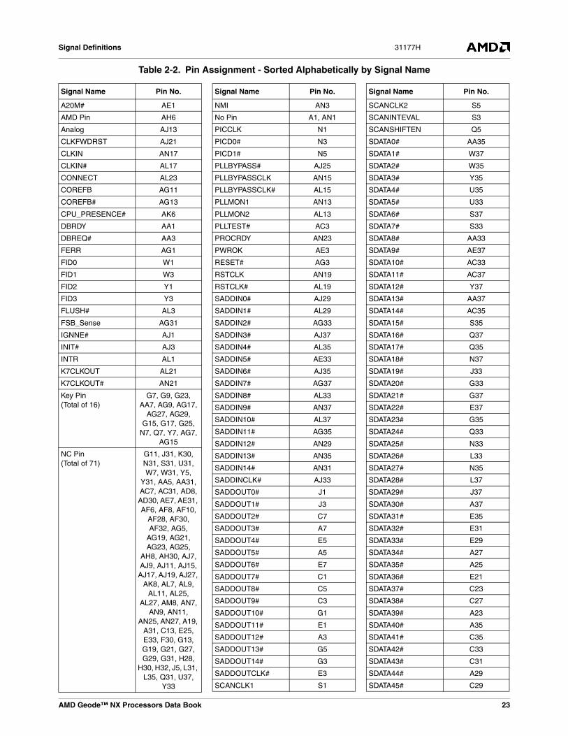
Table 2-1 cross-references Socket A pin locations to signalnames and is sorted by pin number. Other table parame-ters are:
• Signal Name (Abbreviation) column - The full signal name and the abbreviation name used in the pin diagrams (Figure 2-2 on page 15 and Figure 2-3 on page 16).
• Level column - Shows the electrical specification for this pin. — “P” indicates a push-pull mode driven by a single
source. — “O” indicates open-drain mode that allows devices to
share the pin.
Note: The Geode NX processor supports push-pull driv-ers. For more information, see Section 2.1.2"Push-Pull (PP) Drivers" on page 14.
• Port column - Shows the signal type:— “I” indicates input,— “O” indicates output,— “B” indicates bidirectional,
• Ref. (Reference) column - Indicates if this signal should be referenced to VSS (G) or VCC_CORE (P) planes for the purpose of signal routing with respect to the current return paths.
• A “–” is used to indicate that the description is not appli-cable for the pin.
Table 2-1. Pin Assignment - Sorted by Pin Number
Pin No. Signal Name (Abbreviation) Level Port Ref.
A1 No Pin - - -
A3 SADDOUT12# (SAO12#) P O G
A5 SADDOUT5# (SAO5#) P O G
A7 SADDOUT3# (SAO3#) P O G
A9 SDATA55# (SD55#) P B P
A11 SDATA61# (SD61#) P B P
A13 SDATA53# (SD53#) P B G
A15 SDATA63# (SD63#) P B G
A17 SDATA62# (SD62#) P B G
A19 NC Pin - - -
A21 SDATA57# (SD57#) P B G
A23 SDATA39# (SD39#) P B G
A25 SDATA35# (SD35#) P B P
A27 SDATA34# (SD34#) P B P
A29 SDATA44# (SD44#) P B G
A31 NC Pin - - -
A33 SDATAOUTCLK2# (SDOC2#) P O P
A35 SDATA40# (SD40#) P B G
A37 SDATA30# (SD30#) P B P
B2 VSS - - -
B4 VCC_CORE (VCC) - - -
B6 VSS - - -
B8 VCC_CORE (VCC) - - -
B10 VSS - - -
B12 VCC_CORE (VCC) - - -
B14 VSS - - -
B16 VCC_CORE (VCC) - - -
B18 VSS - - -
B20 VCC_CORE (VCC) - - -
B22 VSS - - -
B24 VCC_CORE (VCC) - - -
B26 VSS - - -
B28 VCC_CORE (VCC) - - -
B30 VSS - - -
B32 VCC_CORE (VCC) - - -
B34 VSS - - -
B36 VCC_CORE (VCC) - - -
C1 SADDOUT7# (SAO7#) P O G
C3 SADDOUT9# (SAO9#) P O G
C5 SADDOUT8# (SAO8#) P O G
C7 SADDOUT2# (SAO2#) P O G
C9 SDATA54# (SD54#) P B P
C11 SDATAOUTCLK3# (SDOC3#) P O G
C13 NC Pin - - -
C15 SDATA51# (SD51#) P B P
C17 SDATA60# (SD60#) P B G
C19 SDATA59# (SD59#) P B G
C21 SDATA56# (SD56#) P B G
C23 SDATA37# (SD37#) P B P
C25 SDATA47# (SD47#) P B G
C27 SDATA38# (SD38#) P B G
C29 SDATA45# (SD45#) P B G
C31 SDATA43# (SD43#) P B G
C33 SDATA42# (SD42) P B G
C35 SDATA41# (SD41#) P B G
C37 SDATAOUTCLK1# (SDOC1#) P O G
D2 VCC_CORE (VCC) - - -
D4 VCC_CORE (VCC) - - -
D6 VSS - - -
D8 VCC_CORE (VCC) - - -
D10 VSS - - -
D12 VCC_CORE (VCC) - - -
Pin No. Signal Name (Abbreviation) Level Port Ref.
AMD Geode™ NX Processors Data Book 17

Signal Definitions31177H
Table 2-1. Pin Assignment - Sorted by Pin Number (Continued)
D14 VSS - - -
D16 VCC_CORE (VCC) - - -
D18 VSS - - -
D20 VCC_CORE (VCC) - - -
D22 VSS - - -
D24 VCC_CORE (VCC) - - -
D26 VSS - - -
D28 VCC_CORE (VCC) - - -
D30 VSS - - -
D32 VCC_CORE (VCC) - - -
D34 VSS - - -
D36 VSS - - -
E1 SADDOUT11# (SAO11#) P O P
E3 SADDOUTCLK# (SAOC#) P O G
E5 SADDOUT4# (SAO4#) P O P
E7 SADDOUT6# (SAO6#) P O G
E9 SDATA52# (SD52#) P B P
E11 SDATA50# (SD50#) P B P
E13 SDATA49# (SD49#) P B G
E15 SDATAINCLK3# (SDIC3#) P I G
E17 SDATA48# (SD48#) P B P
E19 SDATA58# (SD58#) P B G
E21 SDATA36# (SD36#) P B P
E23 SDATA46# (SD46#) P B P
E25 NC Pin - - -
E27 SDATAINCLK2# (SDIC2#) P I G
E29 SDATA33# (SD33#) P B P
E31 SDATA32# (SD32#) P B P
E33 NC Pin - - -
E35 SDATA31# (SD31#) P B P
E37 SDATA22# (SD22#) P B G
F2 VSS - - -
F4 VSS - - -
F6 VSS - - -
F8 SOFTVID0 (SVID0) O O -
F10 VSS - - -
F12 VCC_CORE (VCC) - - -
F14 VSS - - -
F16 VCC_CORE (VCC) - - -
F18 VSS - - -
F20 VCC_CORE (VCC) - - -
F22 VSS - - -
F24 VCC_CORE (VCC) - - -
F26 VSS - - -
Pin No. Signal Name (Abbreviation) Level Port Ref.
F28 VCC_CORE (VCC) - - -
F30 NC Pin - - -
F32 VCC_CORE (VCC) - - -
F34 VCC_CORE (VCC) - - -
F36 VCC_CORE (VCC) - - -
G1 SADDOUT10# (SAO10#) P O P
G3 SADDOUT14# (SAO14#) P O G
G5 SADDOUT13# (SAO13#) P O G
G7 Key Pin - - -
G9 Key Pin - - -
G11 NC Pin - - -
G13 NC Pin - - -
G15 Key Pin - - -
G17 Key Pin - - -
G19 NC Pin - - -
G21 NC Pin - - -
G23 Key Pin - - -
G25 Key Pin - - -
G27 NC Pin - - -
G29 NC Pin - - -
G31 NC Pin - - -
G33 SDATA20# (SD20#) P B G
G35 SDATA23# (SD23#) P B G
G37 SDATA21# (SD21#) P B G
H2 VCC_CORE (VCC) - - -
H4 VCC_CORE (VCC) - - -
H6 SOFTVID2 (SVID2) O O -
H8 SOFTVID3 (SVID3) O O -
H10 SOFTVID4 (SVID4) O O -
H12 VCC_CORE (VCC) - - -
H14 VSS - - -
H16 VCC_CORE (VCC) - - -
H18 VSS - - -
H20 VCC_CORE (VCC) - - -
H22 VSS - - -
H24 VCC_CORE (VCC) - - -
H26 VSS - - -
H28 NC Pin - - -
H30 NC Pin - - -
H32 NC Pin - - -
H34 VSS - - -
H36 VSS - - -
J1 SADDOUT0# (SAO0#) P O -
J3 SADDOUT1# (SAO1#) P O -
J5 NC Pin - - -
Pin No. Signal Name (Abbreviation) Level Port Ref.
18 AMD Geode™ NX Processors Data Book

Signal Definitions 31177H
Table 2-1. Pin Assignment - Sorted by Pin Number (Continued)
J7 VID4 O O -
J31 NC Pin - - -
J33 SDATA19# (SD19#) P B G
J35 SDATAINCLK1# (SDIC1#) P I P
J37 SDATA29# (SD29#) P B P
K2 VSS - - -
K4 VSS - - -
K6 VSS - - -
K8 SOFTVID1 (SVID1) O O -
K30 NC Pin - - -
K32 VCC_CORE (VCC) - - -
K34 VCC_CORE (VCC) - - -
K36 VCC_CORE (VCC) - - -
L1 VID0 O O -
L3 VID1 O O -
L5 VID2 O O -
L7 VID3 O O -
L31 NC Pin - - -
L33 SDATA26# (SD26#) P B P
L35 NC Pin - - -
L37 SDATA28# (SD28#) P B P
M2 VCC_CORE (VCC) - - -
M4 VCC_CORE (VCC) - - -
M6 VCC_CORE (VCC) - - -
M8 VCC_CORE (VCC) - - -
M30 VSS - - -
M32 VSS - - -
M34 VSS - - -
M36 VSS - - -
N1 PICCLK 0 I -
N3 PICD0# 0 B -
N5 PICD1# 0 B -
N7 Key Pin - - -
N31 NC Pin - - -
N33 SDATA25# (SD25#) P B P
N35 SDATA27# (SD27#) P B P
N37 SDATA18# (SD18#) P B G
P2 VSS - - -
P4 VSS - - -
P6 VSS - - -
P8 VSS - - -
P30 VCC_CORE (VCC) - - -
P32 VCC_CORE (VCC) - - -
P34 VCC_CORE (VCC) - - -
P36 VCC_CORE (VCC) - - -
Pin No. Signal Name (Abbreviation) Level Port Ref.
Q1 TCK P I -
Q3 TMS P I -
Q5 SCANSHIFTEN (SCNSN) P I -
Q7 Key Pin - - -
Q31 NC Pin - - -
Q33 SDATA24# (SD24#) P B P
Q35 SDATA17# (SD17#) P B G
Q37 SDATA16# (SD16#) P B G
R2 VCC_CORE (VCC) - - -
R4 VCC_CORE (VCC) - - -
R6 VCC_CORE (VCC) - - -
R8 VCC_CORE (VCC) - - -
R30 VSS - - -
R32 VSS - - -
R34 VSS - - -
R36 VSS - - -
S1 SCANCLK1 (SCNCK1) P I -
S3 SCANINTEVAL (SCNINV) P I -
S5 SCANCLK2 (SCNCK2) P I -
S7 THERMDA (THDA) - - -
S31 NC Pin - - -
S33 SDATA7# (SD7#) P B G
S35 SDATA15# (SD15#) P B P
S37 SDATA6# (SD6#) P B G
T2 VSS - - -
T4 VSS - - -
T6 VSS - - -
T8 VSS - - -
T30 VCC_CORE (VCC) - - -
T32 VCC_CORE (VCC) - - -
T34 VCC_CORE (VCC) - - -
T36 VCC_CORE (VCC) - - -
U1 TDI P I -
U3 TRST# P I -
U5 TDO P O -
U7 THERMDC (THDC) - - -
U31 NC Pin - - -
U33 SDATA5# (SD5#) P B G
U35 SDATA4# (SD4#) P B G
U37 NC Pin - - -
V2 VCC_CORE (VCC) - - -
V4 VCC_CORE (VCC) - - -
V6 VCC_CORE (VCC) - - -
V8 VCC_CORE (VCC) - - -
V30 VSS - - -
Pin No. Signal Name (Abbreviation) Level Port Ref.
AMD Geode™ NX Processors Data Book 19
Signal Definitions31177H
Table 2-1. Pin Assignment - Sorted by Pin Number (Continued)
V32 VSS - - -
V34 VSS - - -
V36 VSS - - -
W1 FID0 O O -
W3 FID1 O O -
W5 VREF_SYS (VREF_S) - I -
W7 NC Pin - - -
W31 NC Pin - - -
W33 SDATAINCLK0# (SDIC0#) P I G
W35 SDATA2# (SD2#) P B G
W37 SDATA1# (SD1#) P B P
X2 VSS - - -
X4 VSS - - -
X6 VSS - - -
X8 VSS - - -
X30 VCC_CORE (VCC) - - -
X32 VCC_CORE (VCC) - - -
X34 VCC_CORE (VCC) - - -
X36 VCC_CORE (VCC) - - -
Y1 FID2 O O -
Y3 FID3 O O -
Y5 NC Pin - - -
Y7 Key Pin - - -
Y31 NC Pin - - -
Y33 NC Pin - - -
Y35 SDATA3# (SD3#) P B G
Y37 SDATA12# (SD12#) P B P
Z2 VCC_CORE (VCC) - - -
Z4 VCC_CORE (VCC) - - -
Z6 VCC_CORE (VCC) - - -
Z8 VCC_CORE (VCC) - - -
Z30 VSS - - -
Z32 VSS - - -
Z34 VSS - - -
Z36 VSS - - -
AA1 DBRDY P O -
AA3 DBREQ# P I -
AA5 NC Pin - - -
AA7 Key Pin - - -
AA31 NC Pin - - -
AA33 SDATA8# (SD8#) P B P
AA35 SDATA0# (SD0#) P B G
AA37 SDATA13# (SD13#) P B G
AB2 VSS - - -
AB4 VSS - - -
Pin No. Signal Name (Abbreviation) Level Port Ref.
AB6 VSS - - -
AB8 VSS - - -
AB30 VCC_CORE (VCC) - - -
AB32 VCC_CORE (VCC) - - -
AB34 VCC_CORE (VCC) - - -
AB36 VCC_CORE (VCC) - - -
AC1 STPCLK# (STPC#) P I -
AC3 PLLTEST# (PLTST#) P I -
AC5 ZN P - -
AC7 NC Pin - - -
AC31 NC Pin - - -
AC33 SDATA10# (SD10#) P B P
AC35 SDATA14# (SD14#) P B G
AC37 SDATA11# (SD11#) P B G
AD2 VCC_CORE (VCC) - - -
AD4 VCC_CORE (VCC) - - -
AD6 VCC_CORE (VCC) - - -
AD8 NC Pin - - -
AD30 NC Pin - - -
AD32 VSS - - -
AD34 VSS - - -
AD36 VSS - - -
AE1 A20M# P I -
AE3 PWROK P I -
AE5 ZP P - -
AE7 NC Pin - - -
AE31 NC Pin - - -
AE33 SADDIN5# (SAI5#) P I G
AE35 SDATAOUTCLK0# (SDOC0#) P O P
AE37 SDATA9# (SD9#) P B G
AF2 VSS - - -
AF4 VSS - - -
AF6 NC Pin - - -
AF8 NC Pin - - -
AF10 NC Pin - - -
AF12 VSS - - -
AF14 VCC_CORE (VCC) - - -
AF16 VSS - - -
AF18 VCC_CORE (VCC) - - -
AF20 VSS - - -
AF22 VCC_CORE (VCC) - - -
AF24 VSS - - -
AF26 VCC_CORE (VCC) - - -
AF28 NC Pin - - -
AF30 NC Pin - - -
Pin No. Signal Name (Abbreviation) Level Port Ref.
20 AMD Geode™ NX Processors Data Book

Signal Definitions 31177H
Table 2-1. Pin Assignment - Sorted by Pin Number (Continued)
AF32 NC Pin - - -
AF34 VCC_CORE (VCC) - - -
AF36 VCC_CORE (VCC) - - -
AG1 FERR P O -
AG3 RESET# - I -
AG5 NC Pin - - -
AG7 Key Pin - - -
AG9 Key Pin - - -
AG11 COREFB - - -
AG13 COREFB# - - -
AG15 Key Pin - - -
AG17 Key Pin - - -
AG19 NC Pin - - -
AG21 NC Pin - - -
AG23 NC Pin - - -
AG25 NC Pin - - -
AG27 Key Pin - - -
AG29 Key Pin - - -
AG31 FSB_Sense (FSB) - O G
AG33 SADDIN2# (SAI2#) P I G
AG35 SADDIN11# (SAI11#) P I G
AG37 SADDIN7# (SAI7#) P I P
AH2 VCC_CORE (VCC) - - -
AH4 VCC_CORE (VCC) - - -
AH6 AMD Pin - - -
AH8 NC Pin - - -
AH10 VCC_CORE (VCC) - - -
AH12 VSS - - -
AH14 VCC_CORE (VCC) - - -
AH16 VSS - - -
AH18 VCC_CORE (VCC) - - -
AH20 VSS - - -
AH22 VCC_CORE (VCC) - - -
AH24 VSS - - -
AH26 VCC_CORE (VCC) - - -
AH28 VSS - - -
AH30 NC Pin - - -
AH32 VSS - - -
AH34 VSS - - -
AH36 VSS - - -
AJ1 IGNNE# P I -
AJ3 INIT# P I -
AJ5 VCC_CORE (VCC) - - -
AJ7 NC Pin - - -
AJ9 NC Pin - - -
Pin No. Signal Name (Abbreviation) Level Port Ref.
AJ11 NC Pin - - -
AJ13 Analog (ANLOG) - - -
AJ15 NC Pin - - -
AJ17 NC Pin - - -
AJ19 NC Pin - - -
AJ21 CLKFWDRST (CLKFR) P I P
AJ23 VCCA - - -
AJ25 PLLBYPASS# (PLBYP#) P I -
AJ27 NC Pin - - -
AJ29 SADDIN0# (SAI0#) P I -
AJ31 SFILLVALID# (SFILLV#) P I G
AJ33 SADDINCLK# (SAIC#) P I G
AJ35 SADDIN6# (SAI6#) P I P
AJ37 SADDIN3# (SAI3#) P I G
AK2 VSS - - -
AK4 VSS - - -
AK6 CPU_PRESENCE# (CPR#) - - -
AK8 NC Pin - - -
AK10 VCC_CORE (VCC) - - -
AK12 VSS - - -
AK14 VCC_CORE (VCC) - - -
AK16 VSS - - -
AK18 VCC_CORE (VCC) - - -
AK20 VSS - - -
AK22 VCC_CORE (VCC) - - -
AK24 VSS - - -
AK26 VCC_CORE (VCC) - - -
AK28 VSS - - -
AK30 VCC_CORE (VCC) - - -
AK32 VSS - - -
AK34 VCC_CORE (VCC) - - -
AK36 VCC_CORE (VCC) - - -
AL1 INTR P I -
AL3 FLUSH# P I -
AL5 VCC_CORE (VCC) - - -
AL7 NC Pin - - -
AL9 NC Pin - - -
AL11 NC Pin - - -
AL13 PLLMON2 (PLMN2) O O -
AL15 PLLBYPASSCLK# (PLBYC#) P I -
AL17 CLKIN# P I P
AL19 RSTCLK# (RCLK#) P I P
AL21 K7CLKOUT (K7CO) P O -
AL23 CONNECT (CNNCT) P I P
AL25 NC Pin - - -
Pin No. Signal Name (Abbreviation) Level Port Ref.
AMD Geode™ NX Processors Data Book 21
Signal Definitions31177H
Table 2-1. Pin Assignment - Sorted by Pin Number (Continued)
AL27 NC Pin - - -
AL29 SADDIN1# (SAI1#) P I -
AL31 SDATAOUTVALID# (SDOV#) P I P
AL33 SADDIN8# (SAI8#) P I P
AL35 SADDIN4# (SAI4#) P I G
AL37 SADDIN10# (SAI10#) P I G
AM2 VCC_CORE (VCC) - - -
AM4 VSS - - -
AM6 VSS - - -
AM8 NC Pin - - -
AM10 VCC_CORE (VCC) - - -
AM12 VSS - - -
AM14 VCC_CORE (VCC) - - -
AM16 VSS - - -
AM18 VCC_CORE (VCC) - - -
AM20 VSS - - -
AM22 VCC_CORE (VCC) - - -
AM24 VSS - - -
AM26 VCC_CORE (VCC) - - -
AM28 VSS - - -
AM30 VCC_CORE (VCC) - - -
AM32 VSS - - -
AM34 VCC_CORE (VCC) - - -
AM36 VSS - - -
AN1 No Pin - - -
AN3 NMI P I -
AN5 SMI# P I -
AN7 NC Pin - - -
AN9 NC Pin - - -
AN11 NC Pin - - -
AN13 PLLMON1 (PLMN1) O B -
Pin No. Signal Name (Abbreviation) Level Port Ref.
AN15 PLLBYPASSCLK (PLBYC) P I -
AN17 CLKIN P I P
AN19 RSTCLK (RCLK) P I P
AN21 K7CLKOUT# (K7CO#) P O -
AN23 PROCRDY (PRCRDY) P O P
AN25 NC Pin - - -
AN27 NC Pin - - -
AN29 SADDIN12# (SAI12#) P I G
AN31 SADDIN14# (SAI14#) P I G
AN33 SDATAINVALID# (SDINV#) P I P
AN35 SADDIN13# (SAI13#) P I G
AN37 SADDIN9# (SAI9#) P I G
Pin No. Signal Name (Abbreviation) Level Port Ref.
22 AMD Geode™ NX Processors Data Book
Signal Definitions 31177H
Table 2-2. Pin Assignment - Sorted Alphabetically by Signal Name
AMD Geode™ NX Processors Data Book 23
Signal Name Pin No.
A20M# AE1
AMD Pin AH6
Analog AJ13
CLKFWDRST AJ21
CLKIN AN17
CLKIN# AL17
CONNECT AL23
COREFB AG11
COREFB# AG13
CPU_PRESENCE# AK6
DBRDY AA1
DBREQ# AA3
FERR AG1
FID0 W1
FID1 W3
FID2 Y1
FID3 Y3
FLUSH# AL3
FSB_Sense AG31
IGNNE# AJ1
INIT# AJ3
INTR AL1
K7CLKOUT AL21
K7CLKOUT# AN21
Key Pin(Total of 16)
G7, G9, G23, AA7, AG9, AG17,
AG27, AG29, G15, G17, G25,
N7, Q7, Y7, AG7, AG15
NC Pin(Total of 71)
G11, J31, K30, N31, S31, U31, W7, W31, Y5,
Y31, AA5, AA31, AC7, AC31, AD8, AD30, AE7, AE31, AF6, AF8, AF10,
AF28, AF30, AF32, AG5,
AG19, AG21, AG23, AG25,
AH8, AH30, AJ7, AJ9, AJ11, AJ15,
AJ17, AJ19, AJ27, AK8, AL7, AL9,
AL11, AL25, AL27, AM8, AN7,
AN9, AN11, AN25, AN27, A19,
A31, C13, E25, E33, F30, G13, G19, G21, G27, G29, G31, H28,
H30, H32, J5, L31, L35, Q31, U37,
Y33
NMI AN3
No Pin A1, AN1
PICCLK N1
PICD0# N3
PICD1# N5
PLLBYPASS# AJ25
PLLBYPASSCLK AN15
PLLBYPASSCLK# AL15
PLLMON1 AN13
PLLMON2 AL13
PLLTEST# AC3
PROCRDY AN23
PWROK AE3
RESET# AG3
RSTCLK AN19
RSTCLK# AL19
SADDIN0# AJ29
SADDIN1# AL29
SADDIN2# AG33
SADDIN3# AJ37
SADDIN4# AL35
SADDIN5# AE33
SADDIN6# AJ35
SADDIN7# AG37
SADDIN8# AL33
SADDIN9# AN37
SADDIN10# AL37
SADDIN11# AG35
SADDIN12# AN29
SADDIN13# AN35
SADDIN14# AN31
SADDINCLK# AJ33
SADDOUT0# J1
SADDOUT1# J3
SADDOUT2# C7
SADDOUT3# A7
SADDOUT4# E5
SADDOUT5# A5
SADDOUT6# E7
SADDOUT7# C1
SADDOUT8# C5
SADDOUT9# C3
SADDOUT10# G1
SADDOUT11# E1
SADDOUT12# A3
SADDOUT13# G5
SADDOUT14# G3
SADDOUTCLK# E3
SCANCLK1 S1
Signal Name Pin No.
SCANCLK2 S5
SCANINTEVAL S3
SCANSHIFTEN Q5
SDATA0# AA35
SDATA1# W37
SDATA2# W35
SDATA3# Y35
SDATA4# U35
SDATA5# U33
SDATA6# S37
SDATA7# S33
SDATA8# AA33
SDATA9# AE37
SDATA10# AC33
SDATA11# AC37
SDATA12# Y37
SDATA13# AA37
SDATA14# AC35
SDATA15# S35
SDATA16# Q37
SDATA17# Q35
SDATA18# N37
SDATA19# J33
SDATA20# G33
SDATA21# G37
SDATA22# E37
SDATA23# G35
SDATA24# Q33
SDATA25# N33
SDATA26# L33
SDATA27# N35
SDATA28# L37
SDATA29# J37
SDATA30# A37
SDATA31# E35
SDATA32# E31
SDATA33# E29
SDATA34# A27
SDATA35# A25
SDATA36# E21
SDATA37# C23
SDATA38# C27
SDATA39# A23
SDATA40# A35
SDATA41# C35
SDATA42# C33
SDATA43# C31
SDATA44# A29
SDATA45# C29
Signal Name Pin No.

Signal Definitions31177H
Table 2-2. Pin Assignment - Sorted Alphabetically by Signal Name (Continued)
SDATA46# E23
SDATA47# C25
SDATA48# E17
SDATA49# E13
SDATA50# E11
SDATA51# C15
SDATA52# E9
SDATA53# A13
SDATA54# C9
SDATA55# A9
SDATA56# C21
SDATA57# A21
SDATA58# E19
SDATA59# C19
SDATA60# C17
SDATA61# A11
SDATA62# A17
SDATA63# A15
SDATAINCLK0# W33
SDATAINCLK1# J35
SDATAINCLK2# E27
SDATAINCLK3# E15
SDATAINVALID# AN33
SDATAOUTCLK0# AE35
SDATAOUTCLK1# C37
SDATAOUTCLK2# A33
SDATAOUTCLK3# C11
SDATAOUTVALID# AL31
SFILLVALID# AJ31
SMI# AN5
SOFTVID0 F8
SOFTVID1 K8
SOFTVID2 H6
SOFTVID3 H8
SOFTVID4 H10
STPCLK# AC1
TCK Q1
TDI U1
TDO U5
THERMDA S7
THERMDC U7
TMS Q3
TRST# U3
Signal Name Pin No.
VCC_CORE
(Total of 101)B12, B16, B20,
B28, B32, D2, D4, D8, D12, D16,
D20, D24, D28, D32, F12, F16, F20, F24, F28, F32, F34, F36,
H2, H4, H12, H16, H20, H24, K32,
K34, K36, M2, M4, M6, M8, P30, P32, P34, P36, R2, R4, R6, R8, T30, T32, T34, T36, V2, V4, V6, V8, X30, X32, X34, X36, Z2, Z4,
Z6, Z8, AB30, AB32, AB34,
AB36, AD2, AD4, AD6, AF14, AF18,
AF22, AF26, AF34, AF36, AH2,
AH4, AH10, AH14, AH18,
AH22, AH26, AJ5, AK10, AK14, AK18, AK22, AK26, AK30,
AK34, AK36, AL5, AM2, AM10,
AM14, AM18, AM22, AM26,
AM30, AM34, B4, B8, B24, B36,
VCCA AJ23
VID0 L1
VID1 L3
VID2 L5
VID3 L7
VID4 J7
VREF_SYS W5
Signal Name Pin No.
VSS
(Total of 101)B2, B6, B10, B14,
B18, B22, B26, B30, B34, D6,
D10, D14, D18, D22, D26, D30,
D34, D36, F2, F4, F6, F10, F14, F18,
F22, F26, H14, H18, H22, H26,
H34, H36, K2, K4, K6, M30, M32,
M34, M36, P2, P4, P6, P8, R30, R32, R34, R36, T2, T4, T6, T8, V30, V32, V34, V36, X2, X4, X6, X8, Z30, Z32,
Z34, Z36, AB2, AB4, AB6, AB8,
AD32, AD34, AD36, AF2, AF4,
AF12, AF16, AF20, AF24, AH12, AH16, AH20, AH24, AH28, AH32,
AH34, AH36, AK2, AK4, AK12, AK16,
AK20, AK24, AK28, AK32,
AM4, AM6, AM12, AM16, AM20, AM24, AM28, AM32, AM36
ZN AC5
ZP AE5
Signal Name Pin No.
24 AMD Geode™ NX Processors Data Book
Signal Definitions 31177H
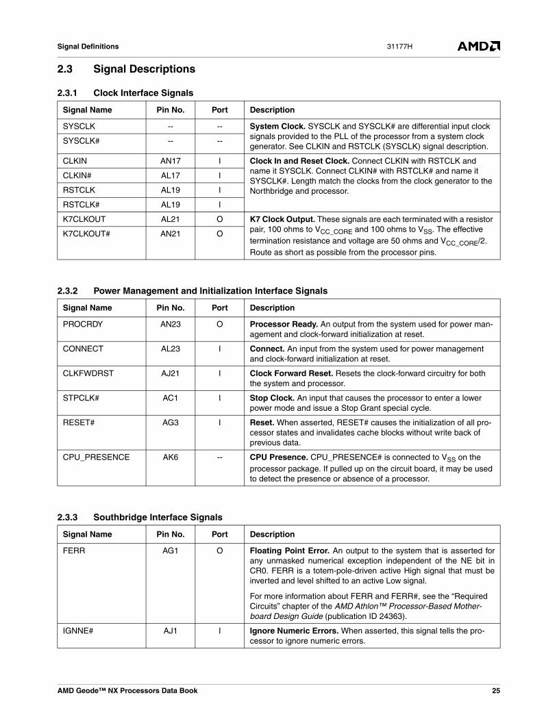
2.3 Signal Descriptions
2.3.1 Clock Interface Signals
Signal Name Pin No. Port Description
SYSCLK -- -- System Clock. SYSCLK and SYSCLK# are differential input clock signals provided to the PLL of the processor from a system clock generator. See CLKIN and RSTCLK (SYSCLK) signal description.
SYSCLK# -- --
CLKIN AN17 I Clock In and Reset Clock. Connect CLKIN with RSTCLK and name it SYSCLK. Connect CLKIN# with RSTCLK# and name it SYSCLK#. Length match the clocks from the clock generator to the Northbridge and processor.
CLKIN# AL17 I
RSTCLK AL19 I
RSTCLK# AL19 I
K7CLKOUT AL21 O K7 Clock Output. These signals are each terminated with a resistor pair, 100 ohms to VCC_CORE and 100 ohms to VSS. The effective termination resistance and voltage are 50 ohms and VCC_CORE/2. Route as short as possible from the processor pins.
K7CLKOUT# AN21 O
2.3.2 Power Management and Initialization Interface Signals
Signal Name Pin No. Port Description
PROCRDY AN23 O Processor Ready. An output from the system used for power man-agement and clock-forward initialization at reset.
CONNECT AL23 I Connect. An input from the system used for power management and clock-forward initialization at reset.
CLKFWDRST AJ21 I Clock Forward Reset. Resets the clock-forward circuitry for both the system and processor.
STPCLK# AC1 I Stop Clock. An input that causes the processor to enter a lower power mode and issue a Stop Grant special cycle.
RESET# AG3 I Reset. When asserted, RESET# causes the initialization of all pro-cessor states and invalidates cache blocks without write back of previous data.
CPU_PRESENCE AK6 -- CPU Presence. CPU_PRESENCE# is connected to VSS on the processor package. If pulled up on the circuit board, it may be used to detect the presence or absence of a processor.
2.3.3 Southbridge Interface Signals
Signal Name Pin No. Port Description
FERR AG1 O Floating Point Error. An output to the system that is asserted forany unmasked numerical exception independent of the NE bit inCR0. FERR is a totem-pole-driven active High signal that must beinverted and level shifted to an active Low signal.
For more information about FERR and FERR#, see the “Required Circuits” chapter of the AMD Athlon™ Processor-Based Mother-board Design Guide (publication ID 24363).
IGNNE# AJ1 I Ignore Numeric Errors. When asserted, this signal tells the pro-cessor to ignore numeric errors.
AMD Geode™ NX Processors Data Book 25
Signal Definitions31177H
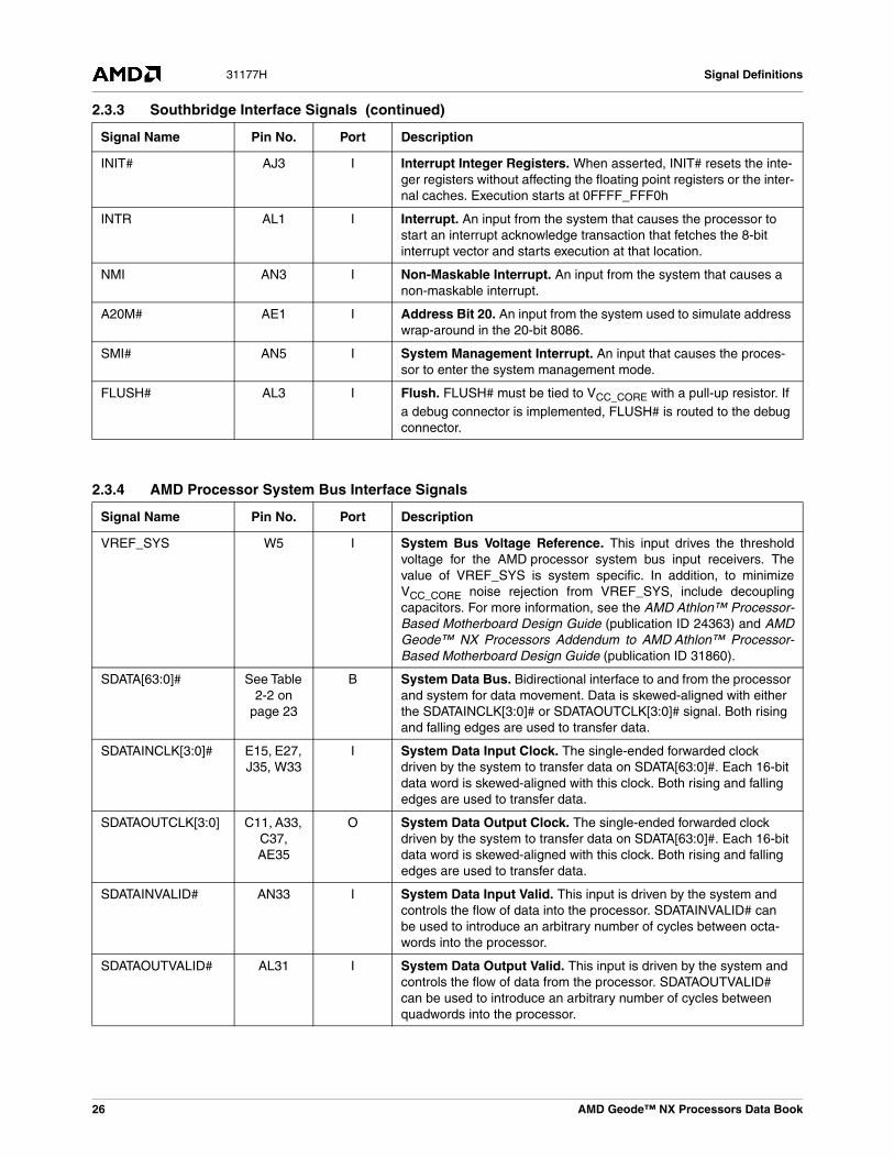
INIT# AJ3 I Interrupt Integer Registers. When asserted, INIT# resets the inte-ger registers without affecting the floating point registers or the inter-nal caches. Execution starts at 0FFFF_FFF0h
INTR AL1 I Interrupt. An input from the system that causes the processor to start an interrupt acknowledge transaction that fetches the 8-bit interrupt vector and starts execution at that location.
NMI AN3 I Non-Maskable Interrupt. An input from the system that causes a non-maskable interrupt.
A20M# AE1 I Address Bit 20. An input from the system used to simulate address wrap-around in the 20-bit 8086.
SMI# AN5 I System Management Interrupt. An input that causes the proces-sor to enter the system management mode.
FLUSH# AL3 I Flush. FLUSH# must be tied to VCC_CORE with a pull-up resistor. If a debug connector is implemented, FLUSH# is routed to the debug connector.
2.3.3 Southbridge Interface Signals (continued)
Signal Name Pin No. Port Description
2.3.4 AMD Processor System Bus Interface Signals
Signal Name Pin No. Port Description
VREF_SYS W5 I System Bus Voltage Reference. This input drives the thresholdvoltage for the AMD processor system bus input receivers. Thevalue of VREF_SYS is system specific. In addition, to minimizeVCC_CORE noise rejection from VREF_SYS, include decouplingcapacitors. For more information, see the AMD Athlon™ Processor-Based Motherboard Design Guide (publication ID 24363) and AMDGeode™ NX Processors Addendum to AMD Athlon™ Processor-Based Motherboard Design Guide (publication ID 31860).
SDATA[63:0]# See Table 2-2 on
page 23
B System Data Bus. Bidirectional interface to and from the processor and system for data movement. Data is skewed-aligned with either the SDATAINCLK[3:0]# or SDATAOUTCLK[3:0]# signal. Both rising and falling edges are used to transfer data.
SDATAINCLK[3:0]# E15, E27, J35, W33
I System Data Input Clock. The single-ended forwarded clock driven by the system to transfer data on SDATA[63:0]#. Each 16-bit data word is skewed-aligned with this clock. Both rising and falling edges are used to transfer data.
SDATAOUTCLK[3:0] C11, A33, C37, AE35
O System Data Output Clock. The single-ended forwarded clock driven by the system to transfer data on SDATA[63:0]#. Each 16-bit data word is skewed-aligned with this clock. Both rising and falling edges are used to transfer data.
SDATAINVALID# AN33 I System Data Input Valid. This input is driven by the system and controls the flow of data into the processor. SDATAINVALID# can be used to introduce an arbitrary number of cycles between octa-words into the processor.
SDATAOUTVALID# AL31 I System Data Output Valid. This input is driven by the system and controls the flow of data from the processor. SDATAOUTVALID# can be used to introduce an arbitrary number of cycles between quadwords into the processor.
26 AMD Geode™ NX Processors Data Book
Signal Definitions 31177H
SFILLVALID# AJ31 I System Bus Fill Valid. When asserted, validates the current mem-ory or I/O data transfer into the processor. The system can tie this pin to the asserted state (validating all fills), or use it to enable or cancel fills as they progress. The processor can sample SFILLVALID# at D0 or D1 (that is, the first or second data beat).
SADDIN[14:2]# See Table 2-2 on
page 23
I System Address Inputs. The unidirectional system address and command interface into the processor from the system. It is used to transfer probes or data movement commands into the processor. All probes and commands on SADDIN[14:2]# are skewed-aligned with the forward clock, SADDINCLK#.
SADDINCLK# AJ33 I System Address Input Clock. The single-ended forwarded clock for SADDIN[14:2]# driven by the system. Both rising and falling edges are used to transfer probes or commands.
SADDOUT[14:2]# See Table 2-2 on
page 23
I System Address Outputs. The unidirectional system address interface from the processor to the system. It is used to transfer pro-cessor commands or probe responses to the system. All commands on SADDOUT[14:0#] are skewed-aligned with the forward clock SADDOUTCLK#.
SADDOUTCLK# E3 I System Address Output Clock. The single-ended forwarded clock for SADDOUT[14:2]# driven by the processor. Both rising and fall-ing edges are used to transfer commands or probe responses.
SADDIN[1:0]# AL29, AJ29
System Address Inputs and Outputs bits 1 and 0. The NX pro-cessor does not support SADDIN[1:0]# or SADDOUT[1:0]#. SAD-DIN[1]# is tied to VCC with pull-up resistors, if this bit is not supported by the Northbridge. SADDOUT[1:0]# are tied to VCC with pull-up resistors if these pins are supported by the Northbridge. For more information, see the AMD Athlon™ Processor System Bus Specification (publication ID 21902).
SADDOUT[1:0]# J3, J1
2.3.4 AMD Processor System Bus Interface Signals (continued)
Signal Name Pin No. Port Description
2.3.5 APIC Interface Signals
Signal Name Pin No. Port Description
PICCLK N1 I APIC Clock and Interrupts. The Advanced Programmable Inter-rupt Controller (APIC) feature provides a flexible and expandablemeans of delivering interrupts in a system using an AMD processor.PICD[1:0]# are the bidirectional message passing signals used forthe APIC and are driven to the Southbridge or a dedicated I/O APIC.PICCLK must be driven with a valid clock input.
Refer to VCC_2.5V Generation Circuit, found in the section, “Moth-erboard Required Circuits” of the AMD Athlon™ Processor-BasedMotherboard Design Guide (publication ID 24363) for the requiredsupporting circuity.
For more information, see Table 5-8 "PICD[1:0]# and PICCLK (APICPins) DC Characteristics" on page 52.
PICD[1:0]# N5, N3 B
AMD Geode™ NX Processors Data Book 27

Signal Definitions31177H
2.3.6 FSB Interface Signals
Signal Name Pin No. Port Description
FSB_Sense AG31 O Front Side Bus Sense. This signal may be used by an external cir-cuit to automatically detect the Front Side Bus (FSB) setting of theprocessor. This pin is always pulled low by the package, indicatingthat the FSB of the processor is 133 MHz.
The FSB_Sense pin is 3.3V tolerant.
2.3.7 Frequency ID Interface Signals
Signal Name Pin No. Port Description
FID[3:0] Y3, Y1, W3, W1
O Frequency Identification Outputs. After PWROK is asserted tothe processor the FID[3:0] pins drive a value of: FID[3:0] = 0110 thatcorresponds to a 6x SYSCLK multiplier for the 133 MHz FSB. Thisinformation is used by the Northbridge to create the SIP (Serial Ini-tialization Packet) stream that the Northbridge sends to the proces-sor after RESET# is de-asserted.
For more information, see Section 3.4 "SYSCLK Multipliers" onpage 42 and Table 5-7 "FID[3:0] DC Characteristics" on page 51.
2.3.8 Thermal Diode Interface Signals
Signal Name Pin No. Port Description
THERMDA S7 -- Thermal Diode Anode and Cathode. These signals are used tomonitor the actual temperature of the processor die, providing moreaccurate temperature control to the system. See Table 5-16 "Ther-mal Diode Electrical Characteristics" on page 59 for more details.
THERMDC U7 --
2.3.9 Voltage Control Interface Signals
Signal Name Pin No. Port Description
COREFB AG11 -- Core Feedback. These are outputs to the system that provide pro-cessor core voltage feedback to the system.COREFB# AG13 --
PWROK AE3 I Power Okay. The PWROK input to the processor must not beasserted until all voltage planes in the system are within specifica-tion and all system clocks are running within specification.
For more information, Section 5.10 "Signal and Power-Up Require-ments" on page 61.
28 AMD Geode™ NX Processors Data Book

Signal Definitions 31177H
SOFTVID[4:0] H10, H8, H6, K8,
F8
O Soft Voltage ID/Voltage ID Mux. AMD PowerNow!™ technologycan use the FID_Change protocol described in Section 4.1 onpage 9 to transition the SOFTVID[4:0] outputs and thereforeVCC_CORE as part of processor performance state transitions.
Note: The NX 1750@14W processor* supports multiple core volt-ages whereas the NX 1500@6W and NX 1250@6W pro-cessors* support only one core voltage (NX 1500@6W =1.0V) (NX 1250@6W = 1.1V).
The VID[4:0] (Voltage ID) and SOFTVID[4:0] (Software driven Volt-age ID) outputs are used by the DC/DC power converter to selectthe processor core voltage. The VID[4:0] pins are shorted to groundor left unconnected on the package and must be pulled up on thecircuit board. The SOFTVID[4:0] pins are open-drain and 2.5V toler-ant.
Refer to the VCC_2.5V Generation Circuit found in the MotherboardRequired Circuits section of the AMD Athlon™ Processor-BasedMotherboard Design Guide (publication ID 24363) for the requiredsupporting circuitry.
The circuit board is required to implement a VID multiplexer toselect a deterministic voltage for the processor at power-up beforethe PWROK input is asserted. Before PWROK is asserted, the VIDmultiplexer drives the VID value from VID[4:0] pins to the DC/DCconverter for VCC_CORE. After PWROK is asserted, the VID multi-plexer drives the VID value from the SOFTVID[4:0] pins to theDC/DC converter for VCC_CORE of the processor. Refer to theAMD Athlon™ Processor-Based Motherboard Design Guide (publi-cation ID 24363) and the AMD Geode™ NX Processors Addendumto AMD Athlon™ Processor-Based Motherboard Design Guide(publication ID 31860) for the recommended VID multiplexer circuit.
The SOFTVID[4:0] pins are driven by the processor to select themaximum VCC_CORE of the processor as reported by the MaximumVID field of the FidVidStatus MSR (MSR C001_0042h) within 20 nsof PWROK assertion. Before PWROK is asserted, theSOFTVID[4:0] outputs are not driven to a deterministic value. TheSOFTVID[4:0] outputs must be used to select VCC_CORE afterPWROK is asserted. Any time the RESET# input is asserted, theSOFTVID[4:0] pins will be driven to select the maximum voltage.
Note: The Start-up VID and Maximum VID fields of the FidVidSta-tus MSR report the same value that corresponds to thenominal voltage that the processor requires to operate atmaximum frequency.
AMD PowerNow! technology can use the FID_Change protocoldescribed in Section 3.1 "Power Management States" on page 33 totransition the SOFTVID[4:0] outputs and therefore VCC_CORE aspart of processor performance state transitions.
The VID codes used by the processor are defined in Table 2-3"SOFTVID[4:0] and VID[4:0] Code to Voltage Definition" on page30.
*The AMD Geode™ NX 1750@14W processor operates at 1.4 GHz, the NX 1500@6W processor operates at 1.0 GHz, and the NX 1250@6W processor operates at 667 MHz. Model numbers reflect performance as described here: http://www.amd.com/connectivitysolutions/geodenxbenchmark.
VID[4:0] J7, L7, L5, L3, L1
O
2.3.9 Voltage Control Interface Signals (continued)
Signal Name Pin No. Port Description
AMD Geode™ NX Processors Data Book 29
Signal Definitions31177H
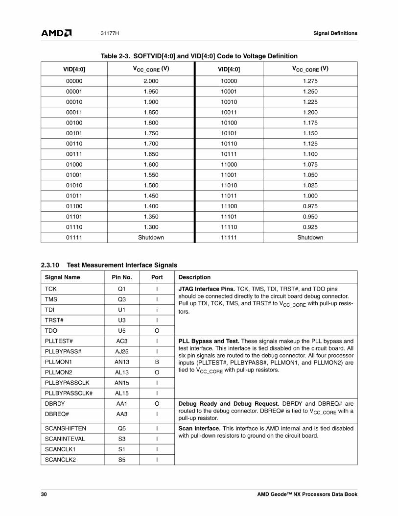
Table 2-3. SOFTVID[4:0] and VID[4:0] Code to Voltage Definition
VID[4:0] VCC_CORE (V) VID[4:0] VCC_CORE (V)
00000 2.000 10000 1.275
00001 1.950 10001 1.250
00010 1.900 10010 1.225
00011 1.850 10011 1.200
00100 1.800 10100 1.175
00101 1.750 10101 1.150
00110 1.700 10110 1.125
00111 1.650 10111 1.100
01000 1.600 11000 1.075
01001 1.550 11001 1.050
01010 1.500 11010 1.025
01011 1.450 11011 1.000
01100 1.400 11100 0.975
01101 1.350 11101 0.950
01110 1.300 11110 0.925
01111 Shutdown 11111 Shutdown
2.3.10 Test Measurement Interface Signals
Signal Name Pin No. Port Description
TCK Q1 I JTAG Interface Pins. TCK, TMS, TDI, TRST#, and TDO pins should be connected directly to the circuit board debug connector. Pull up TDI, TCK, TMS, and TRST# to VCC_CORE with pull-up resis-tors.
TMS Q3 I
TDI U1 i
TRST# U3 I
TDO U5 O
PLLTEST# AC3 I PLL Bypass and Test. These signals makeup the PLL bypass andtest interface. This interface is tied disabled on the circuit board. Allsix pin signals are routed to the debug connector. All four processorinputs (PLLTEST#, PLLBYPASS#, PLLMON1, and PLLMON2) aretied to VCC_CORE with pull-up resistors.
PLLBYPASS# AJ25 I
PLLMON1 AN13 B
PLLMON2 AL13 O
PLLBYPASSCLK AN15 I
PLLBYPASSCLK# AL15 I
DBRDY AA1 O Debug Ready and Debug Request. DBRDY and DBREQ# arerouted to the debug connector. DBREQ# is tied to VCC_CORE with apull-up resistor.
DBREQ# AA3 I
SCANSHIFTEN Q5 I Scan Interface. This interface is AMD internal and is tied disabledwith pull-down resistors to ground on the circuit board.SCANINTEVAL S3 I
SCANCLK1 S1 I
SCANCLK2 S5 I
30 AMD Geode™ NX Processors Data Book
Signal Definitions 31177H
2.3.11 Key Pin, AMD Pin, Analog Pin and No Connect Pins
Signal Name Pin No. Port Description
Key Pins See Table 2-2 on
page 23
-- Key Pins (Total of 16). These 16 locations are for processor type keying for forwards and backwards compatibility. Circuit board designers should treat Key Pins like NC (no connect) Pins. See the NC Pins signal description for more information. A socket designer has the option of creating a top mold piece that allows PGA Key Pins only where designated. However, sockets that populate all 16 Key Pins must be allowed, so the circuit board must always provide for pins at all Key Pin locations.
AMD Pin AH6 -- AMD Pin. AMD Socket A processors do not implement a pin atlocation AH6. All Socket A designs must have a top plate or coverthat blocks this pin location. When the cover plate blocks this loca-tion, a non-AMD part (e.g., PGA370) does not fit into the socket.However, socket manufacturers are allowed to have a contactloaded in the AH6 position. Therefore, circuit board socket designshould account for the possibility that a contact could be loaded inthis position.
The circuit board should treat the AMD Pin (AH6) as an NC Pin. A socket designer has the option of creating a top mold piece that blocks this pin location. However, sockets that populate the AMD pin must be allowed, so the circuit board must always provide for a NC type pin at this pin location. AMD Socket A processors do not implement a pin at location AH6. When a socket that does not pro-vide a pin hole at location AH6 is used, a non-AMD PGA370 part does not fit into Socket A.
Analog Pin AJ13 -- Analog Pin. Treat this pin as a NC.
NC Pins See Table 2-2 on
page 23
-- No Connection Pins (Total of 71). The circuit board should pro-vide a plated hole for an NC pin. The pin hole should not be electri-cally connected to anything.
2.3.12 Power, Ground and Compensation Circuit Connections
Signal Name Pin No. Port Description
VCCA AJ23 -- Power Connection A. VCCA is the processor PLL supply. For infor-mation about the VCCA pin, see Table 5-2 "VCCA Electrical Charac-teristics" on page 47 and the AMD Athlon™ Processor-Based Motherboard Design Guide (publication ID 24363).
VCC_CORE See Table 2-2 on
page 23
-- Power Connection (Total of 101).
VSS See Table 2-2 on
page 23
-- Ground Connection (Total of 101).
ZN AC5 -- Z Negative and Positive. These are the push-pull compensation circuit pins. In Push-Pull mode (selected by the SIP (Serial Initializa-tion Packet) parameter SysPushPull asserted), ZN is tied to VCC_CORE with a resistor that has a resistance matching the imped-ance Z0 of the transmission line. ZP is tied to VSS with a resistor that has a resistance matching the impedance Z0 of the transmission line.
ZP AE5 --
AMD Geode™ NX Processors Data Book 31

Signal Definitions31177H
32 AMD Geode™ NX Processors Data Book

AMD Geode™ NX Processors Data
Power Management 31177H
33.0Power Management
This chapter describes the power management features ofthe AMD Geode™ NX processor. The power managementfeatures of the processor are compliant with the ACPI 1.0band ACPI 2.0 specifications and supportAMD PowerNow!™ technology.
3.1 Power Management StatesThe Geode NX processor has a variety of operating statesthat support different power management goals. In additionto the standard operating state, the processor supportslow-power Halt and Stop Grant states and the FID_Changestate. These states are used by Advanced Configurationand Power Interface (ACPI) enabled operating systems, forprocessor power management. AMD PowerNow! technol-ogy software is used to control processor performance
states with operating systems that do not support ACPI2.0-defined processor performance state control.
Figure 3-1 shows the power management states of the pro-cessor. The figure includes the ACPI “Cx” naming conven-tion for these states.
The sections that follow provide an overview of the powermanagement states. For more details, refer to theAMD Athlon™ Processor System Bus Specification (publi-cation ID 21902).
Note: In all power management states that the processoris powered, the system must not stop the systemclock (SYSCLK/SYSCLK#) to the processor.
Figure 3-1. Processor Power Management States
C1Halt
C0Working4
Execute HLT
SMI#, INTR, NMI, INIT#, RESET#
Incoming Probe
ProbeServiced
STPCLK# asserted
STPCLK# asserted 2
STPCLK# deasserted 3
C2Stop Grant
Cache Snoopable
Incoming Probe
Probe ServicedProbeState1
STPCLK#deasserted
(Read PLVL2 registeror throttling)
C3/S1Stop Grant
Cache Not Snoopable Sleep
STPCLK# asserted
STPCLK# deasserted
FID_Change
Write to FidVidCtl MSR
SIP Stream and System Bus Connect
Note: The System Bus is connected during the following states:1) The Probe state 2) During transitions between the Halt state and the C2 Stop Grant state3) During transitions between the C2 Stop Grant state and the Halt state4) C0 Working state
Software transitionsHardware transitions
Legend
Book 33
Power Management31177H
3.1.1 Working StateThe Working state is the state in which the processor isexecuting instructions.
3.1.2 Halt StateWhen the processor executes the HLT instruction, the pro-cessor enters the Halt state and issues a Halt special cycleto the AMD processor system bus. The processor onlyenters the low power state dictated by the CLK_Ctl MSR(MSR C001_001Bh) if the system controller (Northbridge)disconnects the AMD processor system bus in response tothe Halt special cycle.
If STPCLK# is asserted, the processor exits the Halt stateand enters the Stop Grant state. The processor initiates asystem bus connect, if it is disconnected, then issues aStop Grant special cycle. When STPCLK# is de-asserted,the processor exits the Stop Grant state and re-enters theHalt state. The processor issues a Halt special cycle whenreentering the Halt state.
The Halt state is exited when the processor detects theassertion of INIT#, INTR, NMI, RESET#, or SMI#, or via alocal APIC interrupt message. When the Halt state is exitedthe processor initiates an AMD processor system bus con-nect if it is disconnected.
3.1.3 Stop Grant StatesThe processor enters the Stop Grant state upon recogni-tion of assertion of the STPCLK# input. After entering theStop Grant state, the processor issues a Stop Grant spe-cial bus cycle on the AMD processor system bus. The pro-cessor is not in a low-power state at this time, because theAMD processor system bus is still connected. After theNorthbridge disconnects the AMD processor system bus inresponse to the Stop Grant special bus cycle, the proces-sor enters a low-power state dictated by the CLK_Ctl MSR(MSR C001_001Bh). If the Northbridge needs to probe theprocessor during the Stop Grant state while the system busis disconnected, it must first connect the system bus. Con-necting the system bus places the processor into thehigher power probe state. After the Northbridge has com-pleted all probes of the processor, the Northbridge mustdisconnect the AMD processor system bus again so thatthe processor can return to the low-power state. During theStop Grant states, the processor latches INIT#, INTR, NMI,SMI#, or a local APIC interrupt message if they areasserted.
The Stop Grant state is exited upon the de-assertion ofSTPCLK# or the assertion of RESET#. When STPCLK# isde-asserted, the processor initiates a connect of theAMD processor system bus if it is disconnected. After theprocessor enters the Working state, any pending interruptsare recognized and serviced and the processor resumesexecution at the instruction boundary where STPCLK# wasinitially recognized. If RESET# is sampled asserted duringthe Stop Grant state, the processor exits the Stop Grantstate and the reset process begins.
There are two mechanisms for asserting STPCLK#: hard-ware and software.
The Southbridge can force STPCLK# assertion for throt-tling to protect the processor from exceeding its maximumcase temperature. Typically this is accomplished by assert-ing the THERM# input to the Southbridge. Throttlingasserts STPCLK# for a percentage of a predefined throt-tling period: STPCLK# is repetitively asserted and de-asserted until THERM# is de-asserted.
Software can force the processor into the Stop Grant stateby accessing ACPI-defined registers typically located in theSouthbridge.
The operating system places the processor into the C2Stop Grant state by reading the P_LVL2 register in theSouthbridge.
If an ACPI Thermal Zone is defined for the processor, theoperating system can initiate throttling with STPCLK#using the ACPI defined P_CNT register in the Southbridge.The Northbridge connects the AMD processor system bus,and the processor enters the Probe state to service cachesnoops during Stop Grant for C2 or throttling.
In C2, probes are allowed, as shown in Figure 3-1 on page33.
• If an ACPI Thermal Zone is defined for the processor, the operating system can initiate throttling with STPCLK# using the ACPI defined P_CNT register in the Southbridge. The Northbridge connects the AMD processor system bus, and the processor enters the Probe state to service cache snoops during Stop Grant for C2 or throttling.
• The operating system places the processor into the C3 Stop Grant state by reading the P_LVL3 register in the Southbridge. In C3, the operating system and North-bridge hardware enforce a policy that prevents the processor from being probed. The Southbridge de-asserts STPCLK# and brings the processor out of the C3 Stop Grant state if a bus master request, interrupt, or any other enabled resume event occurs.
• The Stop Grant state is also entered for the S1, Powered On Suspend, system sleep state based on a write to the SLP_TYP and SLP_EN fields in the ACPI-defined Power Management 1 control register in the Southbridge. During the S1 sleep state, system soft-ware ensures no bus master or probe activity occurs. The Southbridge de-asserts STPCLK# and brings the processor out of the S1 Stop Grant state when any enabled resume event occurs.
34 AMD Geode™ NX Processors Data Book

Power Management 31177H
3.1.4 Probe StateThe Probe state is entered when the Northbridge connectsthe AMD processor system bus to probe the processor (forexample, to snoop the processor caches) when the proces-sor is in the Halt or Stop Grant state. When in the Probestate, the processor responds to a probe cycle in the samemanner as when it is in the Working state. When the probehas been serviced, the processor returns to the same stateas when it entered the Probe state (Halt or Stop Grantstate). When probe activity is completed the processor onlyreturns to a low-power state after the Northbridge discon-nects the AMD processor system bus again.
3.1.5 FID_Change StateThe FID_Change State is part of the AMD processor sys-tem bus FID_Change Protocol. During the FID_Changestate the Frequency Identification (FID[4:0]) code thatdetermines the core frequency of the processor and Volt-age Identification (VID[4:0]) driven on the SOFTVID[4:0]pins are transitioned to change the core frequency andcore voltage of the processor. The NX 1750@14W proces-sor* supports multiple core voltages whereas theNX 1500@6W and NX 1250@6W processors* supportonly one core voltage (NX 1500@6W = 1.0V)(NX 1250@6W = 1.1V).
Note: The FID[3:0] pins of the processor do not transitionas part of the FID_Change protocol.
3.1.6 Processor Performance States and the FID_Change Protocol
The FID_Change protocol is used by AMD PowerNow!software to transition the processor from one performancestate to another. The FID_Change protocol is also used forACPI 2.0-compliant processor performance state control.
Processor performance states are combinations of proces-sor core voltage and core frequency. Processor perfor-mance states are used in embedded systems to optimizethe power consumption of the processor (and thereforebattery powered run-time) based upon processor utiliza-tion.
Table 5-4 "Voltage and Frequency Combinations" on page49. specifies the valid voltage and frequency combinationssupported by the processor based upon the maximum corefrequency and the maximum nominal core voltage.
The core frequency multiplier is determined by a 5-bit Fre-quency ID (FID) code (MSR C001_0041h[4:0]). The corevoltage is determined by a 5-bit Voltage ID (VID) code(MSR C001_0041h[12:8]).
Before PWROK is asserted to the processor, the VID[4:0]outputs of the processor dictate the core voltage level ofthe processor.
After PWROK is asserted, the core voltage of the proces-sor is dictated by the SOFTVID[4:0] outputs. The SOFT-VID[4:0] outputs of the processor are not driven to adeterministic value until after PWROK is asserted to theprocessor. The circuit board therefore must provide a ‘VIDMultiplexer’ to drive the VID[4:0] outputs to the DC/DC con-verter for the core voltage of the processor before PWROKis asserted and drive the SOFTVID[4:0] outputs to theDC/DC converter after PWROK is asserted.
The FID[3:0] signals are valid within 100 ns after PWROKis asserted. The chipset must not sample the FID[3:0] sig-nals until they become valid. For warm reset, the FID[3:0]signals become valid within 100 ns after RESET# isasserted. For signal timing requirements refer to Section5.10 "Signal and Power-Up Requirements" on page 61.
After RESET# is de-asserted, the FID[3:0] outputs are notused to transmit FID information for subsequent softwarecontrolled changes in the operating frequency of the pro-cessor.
Processor performance state transitions are required tooccur as two separate transitions. The order of these tran-sitions depends on whether the transition is to a higher orlower performance state.
When transitioning from a lower performance state to ahigher performance state the order of the transitions is:
1) The FID_Change protocol is used to transition to thehigher voltage, while keeping the frequency fixed atthe current setting.
2) The FID_Change protocol is then used to transition tothe higher frequency, while keeping the voltage fixed atthe higher setting.
When transitioning from a high performance state to alower performance state the order of the transitions is:
1) The FID_Change protocol is used to transition to thelower frequency, while keeping the voltage fixed at itscurrent setting.
2) The FID_Change protocol is then used to transition tothe lower voltage, while keeping the frequency fixed atthe lower setting.
The processor provides two MSRs to support theFID_Change protocol: the FidVidCtl MSR (MSRC001_0041h) and the FidVidStatus MSR (MSRC001_0042h). For a definition of these MSRs and theiruse, refer to the BIOS Requirements for AMD PowerNow™Technology Application Note (publication ID 25264)
AMD Geode™ NX Processors Data Book 35
*The AMD Geode™ NX 1750@14W processor operates at 1.4 GHz, the NX 1500@6W processor operates at 1.0 GHz, and the NX 1250@6W processor operatesat 667 MHz. Model numbers reflect performance as described here: http://www.amd.com/connectivitysolutions/geodenxbenchmark.

Power Management31177H
3.1.6.1 FID_Change Protocol ExampleIn any FID_Change transition, only the core voltage or corefrequency of the processor is transitioned. TwoFID_Change transitions are required to transition the volt-age and frequency to a valid performance state. When thevoltage is being transitioned, the frequency is held constantby transitioning to the same FID[3:0] as the current FIDreported in the FidVidStatus MSR (MSR C001_0042h).
Example1) System software determines that a change in proces-
sor performance state is required.
2) System software executes a WRMSR instruction towrite to the FidVidCtl MSR (MSR C001_0041h) to dic-tate:
– The new VID[4:0] code that will be driven to the DC/DC converter from the SOFTVID[4:0] outputs of the processor that selects the new core voltage level.
– The new FID[4:0] code that will be used by the processor to dictate its new operating frequency.
– A Stop Grant Timeout Count (SGTC[19:0], MSR C001_0041h[51:32]) value that determines how many SYSCLK/SYSCLK# 133 MHz clock periods the processor will remain in the FID_Change state. This time accounts for the time that it takes for the PLL of the processor to lock to the new core frequency and the time that it takes for the core voltage of the processor to ramp to the new value.
3) The FIDCHGRATIO bit (MSR C001_0041h[20]) mustbe set to 1.
4) The VIDC bit (MSR C001_0041h[17]) must be set to 1if the voltage is going to be changed.
5) The FIDC bit (MSR C001_0041h[16]) must be set to 1if the frequency is going to be changed.
6) Writing the SGTC field (MSR C001_0041h[51:32]) to anon-zero value initiates the FID_Change protocol.
On the instruction boundary that the SGTC field of theFidVidCtl MSR is written to a non-zero value, the processorstops code execution and issues a FID_Change specialcycle on the AMD processor system bus.
The FID_Change special cycle has a data encoding of0007_0002h that is passed on SDATA[31:0].
SDATA[36:32] contain the new FID[4:0] code during theFID_Change special cycle. The Northbridge is required tocapture this FID[4:0] code when the FID_Change specialcycle is run.
In response to receiving the FID_Change special cycle, theNorthbridge is required to disconnect. The Northbridgecompletes any in-progress bus cycles and then disable itsarbiter before disconnecting the AMD processor systembus so that it will not initiate a AMD processor system busconnect based on bus master or other activity. The North-bridge must disconnect the AMD processor system bus orthe system will hang because the processor is not execut-ing any operating system or application code and is waitingfor the AMD processor system bus to disconnect so that itcan continue with the FID_Change protocol. The North-bridge initiates an AMD processor system bus disconnectin the usual manner; it de-asserts CONNECT.
The processor allows the disconnect to complete by de-asserting PROCRDY. The Northbridge completes the dis-connect by asserting CLKFWDRST.
Once the AMD processor system bus has been discon-nected in response to a FID_Change special cycle, theNorthbridge is not allowed to initiate a re-connect, the pro-cessor is responsible for the eventual re-connect.
After the AMD processor system bus is disconnected, theprocessor enters a low-power state where the clock grid isramped down by a value specified in the CLK_CTL MSR(MSR C001_001Bh).
After entering the low-power state, the processor will:
• Begin counting down the value that was programmed into the SGTC field.
• Drive the new VID[4:0] value on SOFTVID[4:0], causing its core voltage to transition.
• Drive the new FID[4:0] value to its PLL, causing the PLL to lock to the new core frequency.
When the SGTC count reaches zero, the processor rampsits entire clock grid to full frequency (the PLL is alreadylocked to) and signal that it is ready for the Northbridge totransmit the new SIP (Serial Initialization Packet) streamassociated with the new processor core operating fre-quency. The processor signals this by pulsing PROCRDYhigh and then low.
The Northbridge responds to this high pulse on PROCRDYby pulsing CLKFWDRST low and then transferring a SIPstream as it does after PROCRDY is de-asserted after thede-assertion of RESET#. The difference is that the SIPstream that the Northbridge transmits to the processor nowcorresponds to the FID[4:0] that was transmitted onSDATA[36:32] during the FID_Change special cycle.
After the SIP stream is transmitted, the processor initiatesthe AMD processor system bus connect sequence byasserting PROCRDY. The Northbridge responds by de-asserting CLKFWDRST. The forward clocks are startedand the processor issues a Connect special cycle.
36 AMD Geode™ NX Processors Data Book
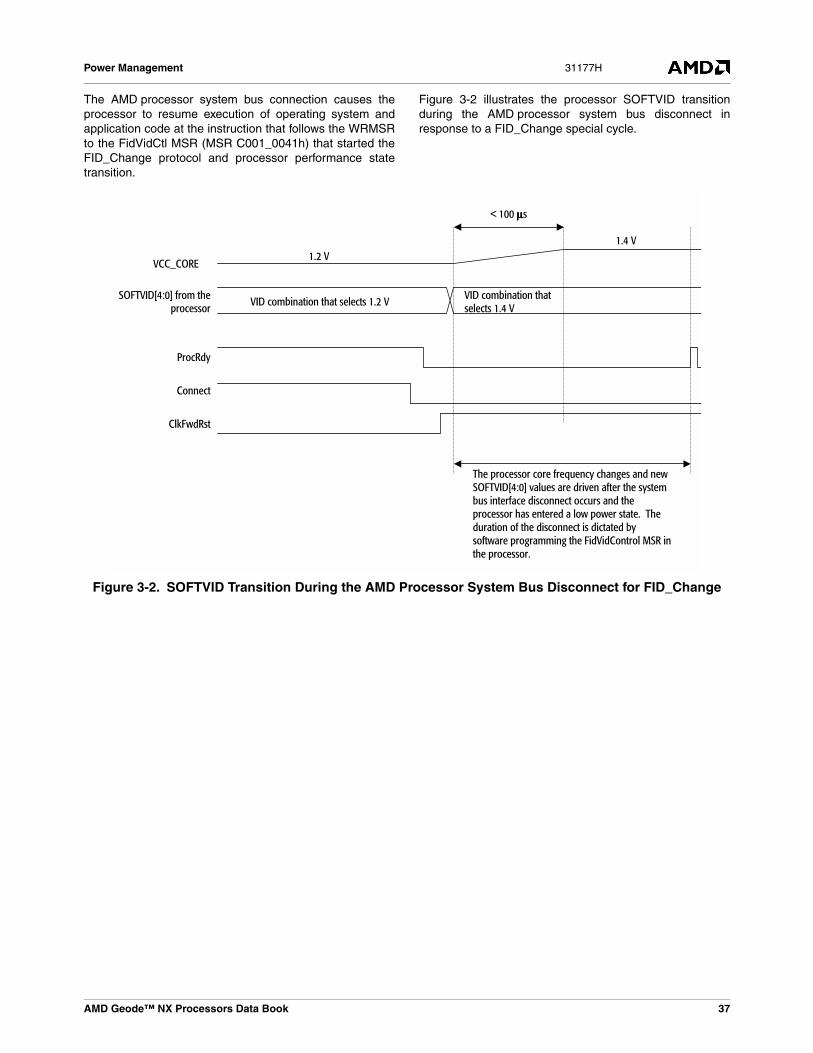
Power Management 31177H
The AMD processor system bus connection causes theprocessor to resume execution of operating system andapplication code at the instruction that follows the WRMSRto the FidVidCtl MSR (MSR C001_0041h) that started theFID_Change protocol and processor performance statetransition.
Figure 3-2 illustrates the processor SOFTVID transitionduring the AMD processor system bus disconnect inresponse to a FID_Change special cycle.
Figure 3-2. SOFTVID Transition During the AMD Processor System Bus Disconnect for FID_Change
1.4 V
VCC_CORE1.2 V
SOFTVID[4:0] from theprocessor
VID combination that selects 1.2 V
< 100 μμμμs
ProcRdy
Connect
ClkFwdRst
VID combination that selects 1.4 V
The processor core frequency changes and new SOFTVID[4:0] values are driven after the system bus interface disconnect occurs and the processor has entered a low power state. The duration of the disconnect is dictated by software programming the FidVidControl MSR in the processor.
AMD Geode™ NX Processors Data Book 37
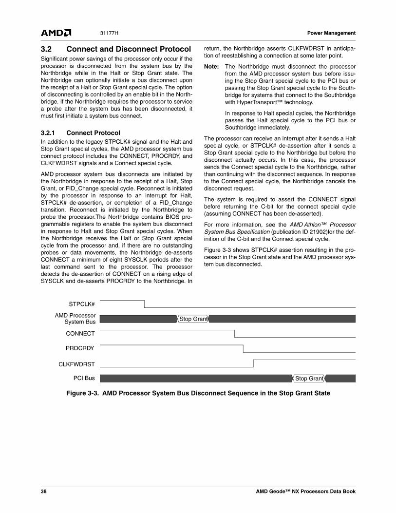
Power Management31177H
3.2 Connect and Disconnect ProtocolSignificant power savings of the processor only occur if theprocessor is disconnected from the system bus by theNorthbridge while in the Halt or Stop Grant state. TheNorthbridge can optionally initiate a bus disconnect uponthe receipt of a Halt or Stop Grant special cycle. The optionof disconnecting is controlled by an enable bit in the North-bridge. If the Northbridge requires the processor to servicea probe after the system bus has been disconnected, itmust first initiate a system bus connect.
3.2.1 Connect ProtocolIn addition to the legacy STPCLK# signal and the Halt andStop Grant special cycles, the AMD processor system busconnect protocol includes the CONNECT, PROCRDY, andCLKFWDRST signals and a Connect special cycle.
AMD processor system bus disconnects are initiated bythe Northbridge in response to the receipt of a Halt, StopGrant, or FID_Change special cycle. Reconnect is initiatedby the processor in response to an interrupt for Halt,STPCLK# de-assertion, or completion of a FID_Changetransition. Reconnect is initiated by the Northbridge toprobe the processor.The Northbridge contains BIOS pro-grammable registers to enable the system bus disconnectin response to Halt and Stop Grant special cycles. Whenthe Northbridge receives the Halt or Stop Grant specialcycle from the processor and, if there are no outstandingprobes or data movements, the Northbridge de-assertsCONNECT a minimum of eight SYSCLK periods after thelast command sent to the processor. The processordetects the de-assertion of CONNECT on a rising edge ofSYSCLK and de-asserts PROCRDY to the Northbridge. In
return, the Northbridge asserts CLKFWDRST in anticipa-tion of reestablishing a connection at some later point.
Note: The Northbridge must disconnect the processorfrom the AMD processor system bus before issu-ing the Stop Grant special cycle to the PCI bus orpassing the Stop Grant special cycle to the South-bridge for systems that connect to the Southbridgewith HyperTransport™ technology.
In response to Halt special cycles, the Northbridgepasses the Halt special cycle to the PCI bus orSouthbridge immediately.
The processor can receive an interrupt after it sends a Haltspecial cycle, or STPCLK# de-assertion after it sends aStop Grant special cycle to the Northbridge but before thedisconnect actually occurs. In this case, the processorsends the Connect special cycle to the Northbridge, ratherthan continuing with the disconnect sequence. In responseto the Connect special cycle, the Northbridge cancels thedisconnect request.
The system is required to assert the CONNECT signalbefore returning the C-bit for the connect special cycle(assuming CONNECT has been de-asserted).
For more information, see the AMD Athlon™ ProcessorSystem Bus Specification (publication ID 21902)for the def-inition of the C-bit and the Connect special cycle.
Figure 3-3 shows STPCLK# assertion resulting in the pro-cessor in the Stop Grant state and the AMD processor sys-tem bus disconnected.
Figure 3-3. AMD Processor System Bus Disconnect Sequence in the Stop Grant State
Stop Grant
Stop Grant
STPCLK#
CONNECT
PROCRDY
CLKFWDRST
PCI Bus
System Bus AMD Processor
38 AMD Geode™ NX Processors Data Book
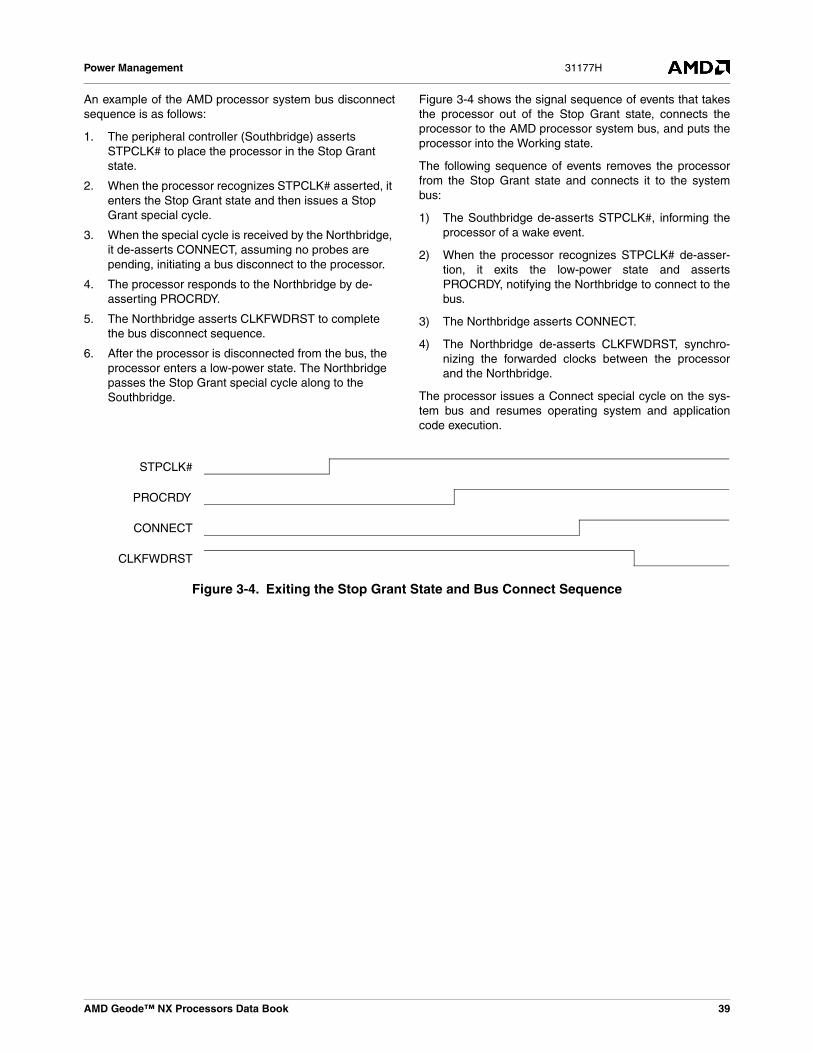
Power Management 31177H
An example of the AMD processor system bus disconnectsequence is as follows:
1. The peripheral controller (Southbridge) asserts STPCLK# to place the processor in the Stop Grant state.
2. When the processor recognizes STPCLK# asserted, it enters the Stop Grant state and then issues a Stop Grant special cycle.
3. When the special cycle is received by the Northbridge, it de-asserts CONNECT, assuming no probes are pending, initiating a bus disconnect to the processor.
4. The processor responds to the Northbridge by de-asserting PROCRDY.
5. The Northbridge asserts CLKFWDRST to complete the bus disconnect sequence.
6. After the processor is disconnected from the bus, the processor enters a low-power state. The Northbridge passes the Stop Grant special cycle along to the Southbridge.
Figure 3-4 shows the signal sequence of events that takesthe processor out of the Stop Grant state, connects theprocessor to the AMD processor system bus, and puts theprocessor into the Working state.
The following sequence of events removes the processorfrom the Stop Grant state and connects it to the systembus:
1) The Southbridge de-asserts STPCLK#, informing theprocessor of a wake event.
2) When the processor recognizes STPCLK# de-asser-tion, it exits the low-power state and assertsPROCRDY, notifying the Northbridge to connect to thebus.
3) The Northbridge asserts CONNECT.
4) The Northbridge de-asserts CLKFWDRST, synchro-nizing the forwarded clocks between the processorand the Northbridge.
The processor issues a Connect special cycle on the sys-tem bus and resumes operating system and applicationcode execution.
Figure 3-4. Exiting the Stop Grant State and Bus Connect Sequence
STPCLK#
PROCRDY
CONNECT
CLKFWDRST
AMD Geode™ NX Processors Data Book 39
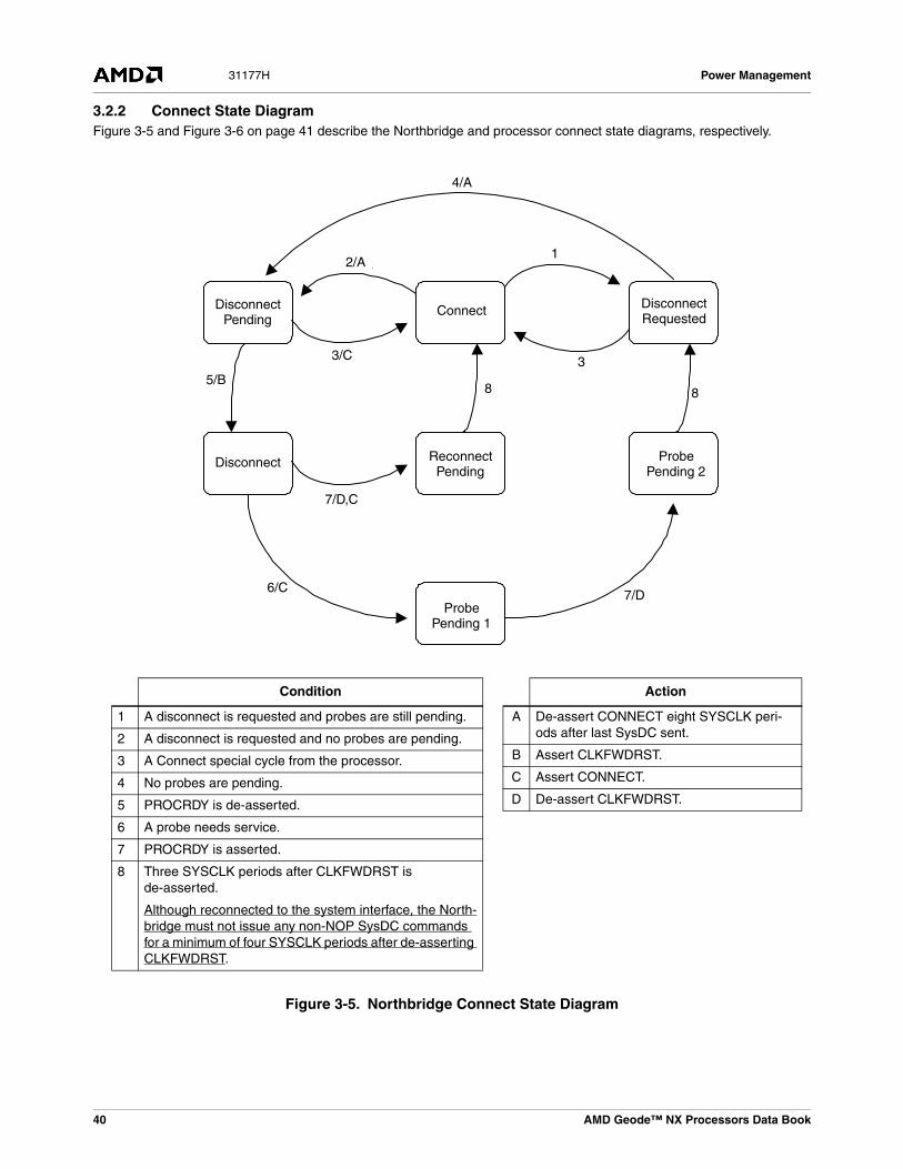
Power Management31177H
3.2.2 Connect State DiagramFigure 3-5 and Figure 3-6 on page 41 describe the Northbridge and processor connect state diagrams, respectively.
Figure 3-5. Northbridge Connect State Diagram
Condition
1 A disconnect is requested and probes are still pending.
2 A disconnect is requested and no probes are pending.
3 A Connect special cycle from the processor.
4 No probes are pending.
5 PROCRDY is de-asserted.
6 A probe needs service.
7 PROCRDY is asserted.
8 Three SYSCLK periods after CLKFWDRST is de-asserted.
Although reconnected to the system interface, the North-bridge must not issue any non-NOP SysDC commands for a minimum of four SYSCLK periods after de-asserting CLKFWDRST.
Action
A De-assert CONNECT eight SYSCLK peri-ods after last SysDC sent.
B Assert CLKFWDRST.
C Assert CONNECT.
D De-assert CLKFWDRST.
DisconnectPending Connect Disconnect
Requested
ReconnectPending
ProbePending 2Disconnect
ProbePending 1
1
3
2/A
4/A
5/B3/C
7/D,C
8
6/C 7/D
8
DisconnectPending
Disconnect
Connect DisconnectRequested
ProbePending 2
ReconnectPending
ProbePending 1
6/C
5/B
2/A
3/C
8
7/D,C
3
8
1
7/D
4/A
40 AMD Geode™ NX Processors Data Book
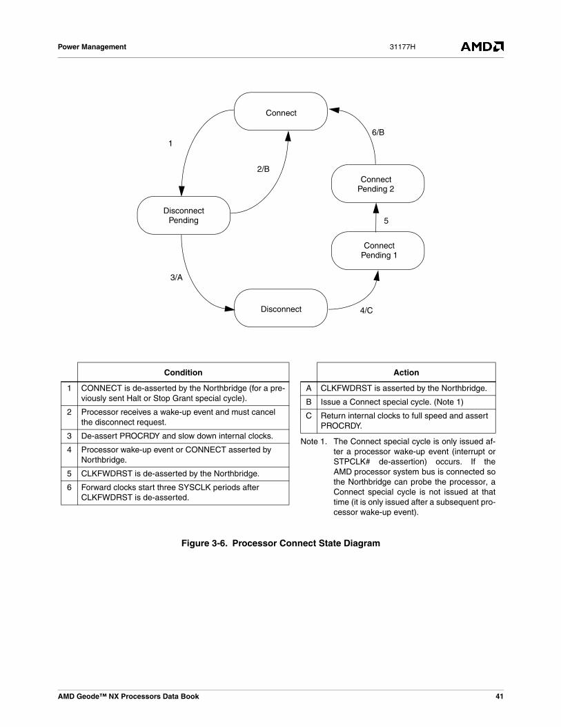
Power Management 31177H
Figure 3-6. Processor Connect State Diagram
Condition
1 CONNECT is de-asserted by the Northbridge (for a pre-viously sent Halt or Stop Grant special cycle).
2 Processor receives a wake-up event and must cancel the disconnect request.
3 De-assert PROCRDY and slow down internal clocks.
4 Processor wake-up event or CONNECT asserted by Northbridge.
5 CLKFWDRST is de-asserted by the Northbridge.
6 Forward clocks start three SYSCLK periods after CLKFWDRST is de-asserted.
Action
A CLKFWDRST is asserted by the Northbridge.
B Issue a Connect special cycle. (Note 1)
Note 1. The Connect special cycle is only issued af-ter a processor wake-up event (interrupt orSTPCLK# de-assertion) occurs. If theAMD processor system bus is connected sothe Northbridge can probe the processor, aConnect special cycle is not issued at thattime (it is only issued after a subsequent pro-cessor wake-up event).
C Return internal clocks to full speed and assert PROCRDY.
Connect
Disconnect
Disconnect
Connect
Connect
1
3/A
4/C
5
6/B
2/B
Pending 2
Pending 1
Pending
AMD Geode™ NX Processors Data Book 41

Power Management31177H
3.3 Clock ControlThe processor implements a Clock Control (CLK_CTL)MSR (MSR C001_001Bh) that determines the internalclock divisor when the AMD processor system bus is dis-connected.
Refer to the AMD Geode™ NX Processors BIOS Consider-ations Application Note (publication ID 32483) and theBIOS Requirements for BIOS Requirements for AMD Pow-erNow™ Technology Application Note (publication ID25264) for more details on the CLK_CTL register.
3.4 SYSCLK MultipliersThe processor provides two mechanisms for communicat-ing processor core operating frequency information to theNorthbridge. These are the processor FID[3:0] outputs andthe FID_Change special cycle. The FID[3:0] outputs spec-ify the core frequency of the processor as a multiple of theinput clock (SYSCLK/SYSCLK#) of the processor. Thisprocessor supports an input clock, or Front Side Bus(FSB), that runs up to 133 MHz.
The FID[3:0] signals are valid after PWROK is asserted.The chipset must not sample the FID[3:0] signals until theybecome valid. The FID[3:0] outputs of the processor pro-vide processor operating frequency information the North-bridge uses when creating the SIP stream the Northbridgesends to the processor after RESET# is de-asserted. TheFID[3:0] outputs always select a 6x SYSCLK multiplier forthe Geode NX processor: FID[3:0] = 0110.
Software uses the FID_Change protocol to transition theprocessor to the desired performance state.
The FID[3:0] outputs are not used as part of theFID_Change protocol and do not change from theirRESET# value during software-controlled processor corefrequency transitions.
The FID_Change special cycle is used to communicateprocessor operating frequency information to the North-bridge during software-controlled processor core voltageand frequency (performance state) transitions. TheFidVidCtl MSR (MSR C001_0041h) allows software tospecify a 5-bit FID value during software-controlled proces-sor performance state transitions. The additional bit allowstransitions to lower SYSCLK multipliers of 3x and 4x aswell as all other SYSCLK multipliers supported by the pro-cessor.
For a description of the FID_Change protocol refer Section3.1.5 on page 35.
Table 3-1 lists the FID[4:0] SYSCLK multiplier codes for theprocessor used by software to dictate the core frequency ofthe processor and the 5-bit value driven on SDATA[36:32]#by the processor during the FID_Change special bus cycle.
Note: Only clock multipliers associated with operatingfrequencies specified in Section 5.0 "ElectricalSpecifications" on page 47 are valid for this pro-cessor. Software distinguishes the speed grade ofthe processor by reading the MFID field of the Fid-VidStatus MSR (MSR C001_0042h).
42 AMD Geode™ NX Processors Data Book
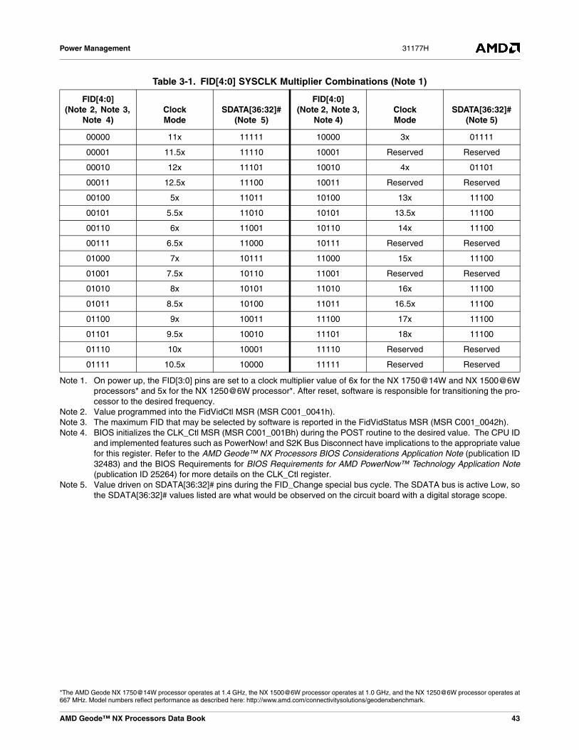
Power Management 31177H
Table 3-1. FID[4:0] SYSCLK Multiplier Combinations (Note 1)
FID[4:0](Note 2, Note 3,
Note 4)ClockMode
SDATA[36:32]#(Note 5)
FID[4:0](Note 2, Note 3,
Note 4)ClockMode
SDATA[36:32]#(Note 5)
00000 11x 11111 10000 3x 01111
00001 11.5x 11110 10001 Reserved Reserved
00010 12x 11101 10010 4x 01101
00011 12.5x 11100 10011 Reserved Reserved
00100 5x 11011 10100 13x 11100
00101 5.5x 11010 10101 13.5x 11100
00110 6x 11001 10110 14x 11100
00111 6.5x 11000 10111 Reserved Reserved
01000 7x 10111 11000 15x 11100
01001 7.5x 10110 11001 Reserved Reserved
01010 8x 10101 11010 16x 11100
01011 8.5x 10100 11011 16.5x 11100
01100 9x 10011 11100 17x 11100
01101 9.5x 10010 11101 18x 11100
01110 10x 10001 11110 Reserved Reserved
01111 10.5x 10000 11111 Reserved Reserved
Note 1. On power up, the FID[3:0] pins are set to a clock multiplier value of 6x for the NX 1750@14W and NX 1500@6Wprocessors* and 5x for the NX 1250@6W processor*. After reset, software is responsible for transitioning the pro-cessor to the desired frequency.
Note 2. Value programmed into the FidVidCtl MSR (MSR C001_0041h). Note 3. The maximum FID that may be selected by software is reported in the FidVidStatus MSR (MSR C001_0042h).Note 4. BIOS initializes the CLK_Ctl MSR (MSR C001_001Bh) during the POST routine to the desired value. The CPU ID
and implemented features such as PowerNow! and S2K Bus Disconnect have implications to the appropriate valuefor this register. Refer to the AMD Geode™ NX Processors BIOS Considerations Application Note (publication ID32483) and the BIOS Requirements for BIOS Requirements for AMD PowerNow™ Technology Application Note(publication ID 25264) for more details on the CLK_Ctl register.
Note 5. Value driven on SDATA[36:32]# pins during the FID_Change special bus cycle. The SDATA bus is active Low, sothe SDATA[36:32]# values listed are what would be observed on the circuit board with a digital storage scope.
AMD Geode™ NX Processors Data Book 43
*The AMD Geode NX 1750@14W processor operates at 1.4 GHz, the NX 1500@6W processor operates at 1.0 GHz, and the NX 1250@6W processor operates at667 MHz. Model numbers reflect performance as described here: http://www.amd.com/connectivitysolutions/geodenxbenchmark.
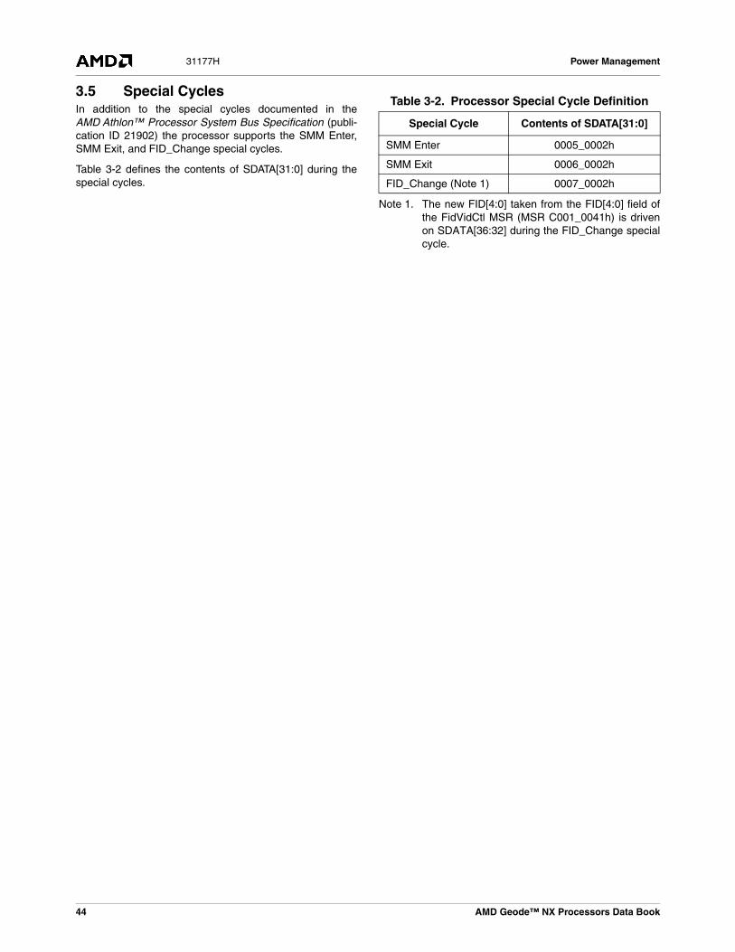
Power Management31177H
3.5 Special CyclesIn addition to the special cycles documented in theAMD Athlon™ Processor System Bus Specification (publi-cation ID 21902) the processor supports the SMM Enter,SMM Exit, and FID_Change special cycles.
Table 3-2 defines the contents of SDATA[31:0] during thespecial cycles.
Table 3-2. Processor Special Cycle Definition
Special Cycle Contents of SDATA[31:0]
SMM Enter 0005_0002h
SMM Exit 0006_0002h
FID_Change (Note 1)
Note 1. The new FID[4:0] taken from the FID[4:0] field ofthe FidVidCtl MSR (MSR C001_0041h) is drivenon SDATA[36:32] during the FID_Change specialcycle.
0007_0002h
44 AMD Geode™ NX Processors Data Book
AMD Geode™ NX Processors Data
CPUID Support 31177H
44.0CPUID Support
The CPUID for the AMD Geode™ NX processors is 681.The processor version and feature set recognition can beperformed through the use of the CPUID instruction thatprovides complete information about the processor—ven-dor, type, name, etc., and its capabilities. Software canmake use of this information to accurately tune the systemfor maximum performance and benefit to users.
For information on the use of the CPUID instruction see:
• AMD Athlon™ and AMD Duron™ Processor Recogni-tion Application Note Addendum (publication ID 21922)
• AMD Processor Recognition Application Note (publica-tion ID 20734)
Book 45

CPUID Support31177H
46 AMD Geode™ NX Processors Data Book

AMD Geode™ NX Processors Data
Electrical Specifications 31177H
55.0Electrical Specifications
This section provides information on electrical connections,absolute maximum ratings, and DC/AC characteristics forthe AMD Geode™ NX processor. All current specified asbeing sourced by the processor is negative. All currentspecified as being sunk by the processor is positive.
5.1 Electrical Connections
5.1.1 NC, AMD, Analog, and Key PinsThe circuit board should provide a plated hole for a NC (NoConnect) pin (total of 71, see Table 2-2 "Pin Assignment -Sorted Alphabetically by Signal Name" on page 23 for pinassignments). The pin hole should not be electrically con-nected to anything.
The AMD Pin (pin AH6), Analog Pin (pin AJ13) and KeyPins (total of 16, see Table 2-2 "Pin Assignment - SortedAlphabetically by Signal Name" on page 23 for pin assign-ments) should be treated like a NC pin.
See Section 2.3.11 "Key Pin, AMD Pin, Analog Pin and NoConnect Pins" on page 31 for more details regarding thesepins.
5.1.2 DecouplingSee the AMD Athlon™ Processor-Based MotherboardDesign Guide (publication ID 24363) and AMD Geode™NX Processors Addendum to AMD Athlon™ Processor-Based Motherboard Design Guide (publication ID 31860),or contact your local AMD FAE (Field Applications Engi-neer) for information about the decoupling required on thecircuit board for use with the Geode NX processors.
5.2 Absolute Maximum RatingsDo not subject the processor to conditions that exceed theabsolute ratings listed in Table 5-1, as such conditions mayadversely affect long-term reliability or result in functionaldamage.
5.3 VCCA Electrical CharacteristicsVCCA (pin AJ23) is the processor PLL supply. Table 5-2provides the voltage and current values for the VCCA pin.
Table 5-1. Absolute Ratings
Symbol Parameter Min Max
VCC_CORE Processor Core Supply –0.5V VCC_CORE_NOM + 0.5V
VCCA Processor PLL Supply –0.5V VCCA_Max + 0.5V
TSTORAGE Storage Temperature of Processor –40ºC 100ºC
Table 5-2. VCCA Electrical Characteristics
Symbol Parameter Min Nom Max Units
VVCCA VCCA Voltage (Note 1) 2.25 2.5 2.75 V
I VVCCA – VCC_CORE I < 1.60V (Note 2)
--
IVCCA VCCA Current (Note 3) 0 50 mA/GHz
Note 1. Minimum and maximum voltages are absolute. No transients below minimum nor above maximum voltages arepermitted.
Note 2. For more information, refer to the AMD Athlon™ Processor-Based Motherboard Design Guide (publication ID24363) and the AMD Geode™ NX Processors Addendum to AMD Athlon™ Processor-Based Motherboard DesignGuide (publication ID 31860)
Note 3. Measured at 2.5V.
Book 47

Electrical Specifications31177H
5.4 VCC_CORE Electrical CharacteristicsTable 5-3 provides the electrical characteristics forVCC_CORE. Figure 5-1 shows the processor core voltage(VCC_CORE) waveform response to perturbation. The time
tMAX_AC (positive AC transient excursion time) representsthe maximum allowable time above the DC tolerancethreshold.
Figure 5-1. VCC_CORE Voltage Waveform
Table 5-3. VCC_CORE Electrical Characteristics
Symbol ParameterLimit
(Note 1) Units
VCC_CORE_AC_MAX Maximum excursion above VCC_CORE_NOM (Note 2) 150 mV
VCC_CORE_DC_MAX Maximum static voltage above VCC_CORE_NOM (Note 2) 100 mV
VCC_CORE_MIN Minimum voltage below VCC_CORE_NOM (Note 2) –50 mV
tMAX_AC Maximum excursion time for AC transients 10 μs
Note 1. All voltage measurements are taken differentially at the COREFB/COREFB# pins while the processor is in theworking state.
Note 2. VCC_CORE nominal values and absolute minimum allowable VCC_CORE voltage for the Geode NX processors isprovided in Table 5-4 "Voltage and Frequency Combinations" on page 49.
VCC_CORE_AC_MAX
tMAX_AC
VCC_CORE_DC_MAX
VCC_CORE_NOM
VCC_CORE_MIN
ICORE_MIN
ICORE_MAX
dI /dt
48 AMD Geode™ NX Processors Data Book

Electrical Specifications 31177H
5.4.1 Valid Voltage and Frequency CombinationsTable 5-4 characterizes the valid voltage and frequencycombinations for the AMD Geode NX processor. The Fre-quency column corresponds to the rated frequency of theprocessor. The Maximum FID (MFID) field in the FidVid-Status MSR (MSR C001_0042h[20:16]) is used by soft-
ware to determine the maximum frequency of theprocessor. Section 3.1 "Power Management States" onpage 33 describes how AMD PowerNow!™ software usesthis information to implement processor performancestates
Table 5-4. Voltage and Frequency Combinations
AMD Geode™ NX Processor(Note 1)
VCC_CORE_NOM Voltage (Note 2, Note 3)
Frequency (Note 4)
NX 1250@6W Processor 1.10V (Note 5) ≤667 MHz
NX 1500@6W Processor 1.00V (Note 6) ≤1000 MHz
NX 1750@14W Processor 1.05V (Note 7) ≤1000 MHz
1.10V 1067 MHz
1.15V 1133 MHz
1.20V 1200 MHz
1.25V 1400 MHz
Note 1. The AMD Geode™ NX 1750@14W processor operates at 1.4 GHz, the NX 1500@6W processor operates at 1.0GHz, and the NX 1250@6W processor operates at 667 MHz. Model numbers reflect performance as describedhere: http://www.amd.com/connectivitysolutions/geodenxbenchmark.
Note 2. All voltages listed are nominal. See Figure 5-1 on page 48 for AC and DC transient voltage tolerances.Note 3. The maximum processor die temperature is 95°C for all voltage and frequency combinations.Note 4. The “≤“ symbol indicates that the BIOS vendor can use any performance state equal to or less than the specified
frequency at a given voltage. Note 5. The absolute minimum voltage, inclusive of all tolerances and excursions, is 1.05V.Note 6. The absolute minimum voltage, inclusive of all tolerances and excursions, is 0.95V.Note 7. The absolute minimum voltage, inclusive of all tolerances and excursions, is 1.00V.
AMD Geode™ NX Processors Data Book 49

Electrical Specifications31177H
5.5 DC Characteristics
Figure 5-2. SYSCLK and SYSCLK# Differential Clock Signals
Table 5-5. SYSCLK and SYSCLK# DC Characteristics (Note 1)
Symbol Parameter Min Max Units
VThreshold-DC Crossing before transition is detected (DC)
400 mV
VThreshold-AC Crossing before transition is detected (AC)
450 mV
ILEAK_P Leakage current through P-channel pull up to VCC_CORE
–250 µA
ILEAK_N Leakage current through N-channel pull down to VSS (Ground)
250 µA
VCROSS Differential signal crossover VCC_CORE/2 +/– 100 mV
CPIN Capacitance (Note 2) 25 pF
Note 1. The SYSCLK signal represents CLKIN and RSTCLK tied together while the SYSCLK# signal represents CLKIN#and RSTCLK# tied together.)
Note 2. The SYSCLK and SYSCLK# signals have twice the listed capacitance because they connect to two input pads (i.e.,CLKIN/RSTCLK and CLKIN#/RSTCLK#).
VCROSS VThreshold-DC = 400 mV VThreshold-AC = 450 mV
50 AMD Geode™ NX Processors Data Book
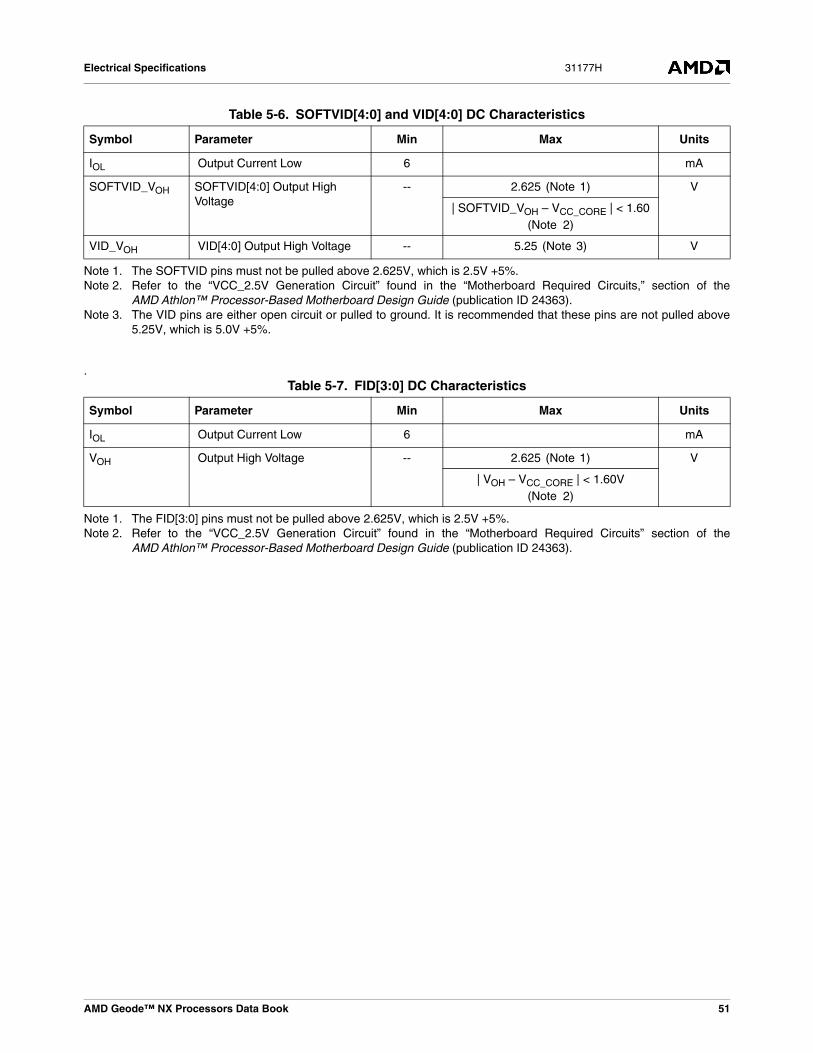
Electrical Specifications 31177H
.
Table 5-6. SOFTVID[4:0] and VID[4:0] DC Characteristics
Symbol Parameter Min Max Units
IOL Output Current Low 6 mA
SOFTVID_VOH SOFTVID[4:0] Output High Voltage
-- 2.625 (Note 1) V
| SOFTVID_VOH – VCC_CORE | < 1.60(Note 2)
VID_VOH VID[4:0] Output High Voltage -- 5.25 (Note 3) V
Note 1. The SOFTVID pins must not be pulled above 2.625V, which is 2.5V +5%.Note 2. Refer to the “VCC_2.5V Generation Circuit” found in the “Motherboard Required Circuits,” section of the
AMD Athlon™ Processor-Based Motherboard Design Guide (publication ID 24363).Note 3. The VID pins are either open circuit or pulled to ground. It is recommended that these pins are not pulled above
5.25V, which is 5.0V +5%.
Table 5-7. FID[3:0] DC Characteristics
Symbol Parameter Min Max Units
IOL Output Current Low 6 mA
VOH Output High Voltage -- 2.625 (Note 1) V
| VOH – VCC_CORE | < 1.60V (Note 2)
Note 1. The FID[3:0] pins must not be pulled above 2.625V, which is 2.5V +5%.Note 2. Refer to the “VCC_2.5V Generation Circuit” found in the “Motherboard Required Circuits” section of the
AMD Athlon™ Processor-Based Motherboard Design Guide (publication ID 24363).
AMD Geode™ NX Processors Data Book 51
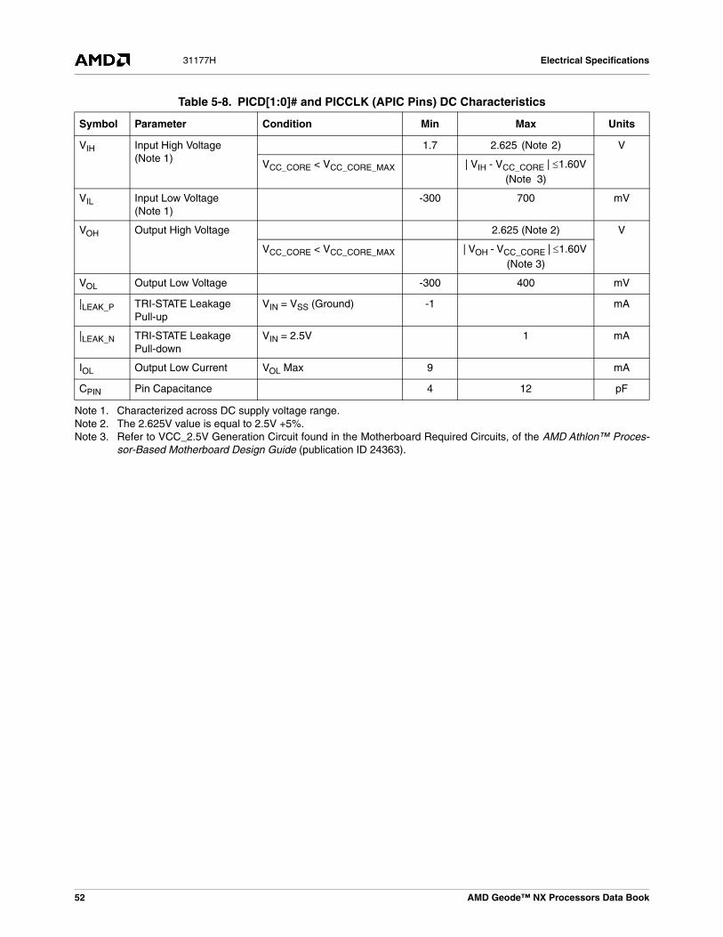
Electrical Specifications31177H
Table 5-8. PICD[1:0]# and PICCLK (APIC Pins) DC Characteristics
Symbol Parameter Condition Min Max Units
VIH Input High Voltage (Note 1)
1.7 2.625 (Note 2) V
VCC_CORE < VCC_CORE_MAX | VIH - VCC_CORE | ≤1.60V (Note 3)
VIL Input Low Voltage (Note 1)
-300 700 mV
VOH Output High Voltage 2.625 (Note 2) V
VCC_CORE < VCC_CORE_MAX | VOH - VCC_CORE | ≤1.60V (Note 3)
VOL Output Low Voltage -300 400 mV
|LEAK_P TRI-STATE Leakage Pull-up
VIN = VSS (Ground) -1 mA
|LEAK_N TRI-STATE Leakage Pull-down
VIN = 2.5V 1 mA
IOL Output Low Current VOL Max 9 mA
CPIN Pin Capacitance 4 12 pF
Note 1. Characterized across DC supply voltage range.Note 2. The 2.625V value is equal to 2.5V +5%.Note 3. Refer to VCC_2.5V Generation Circuit found in the Motherboard Required Circuits, of the AMD Athlon™ Proces-
sor-Based Motherboard Design Guide (publication ID 24363).
52 AMD Geode™ NX Processors Data Book
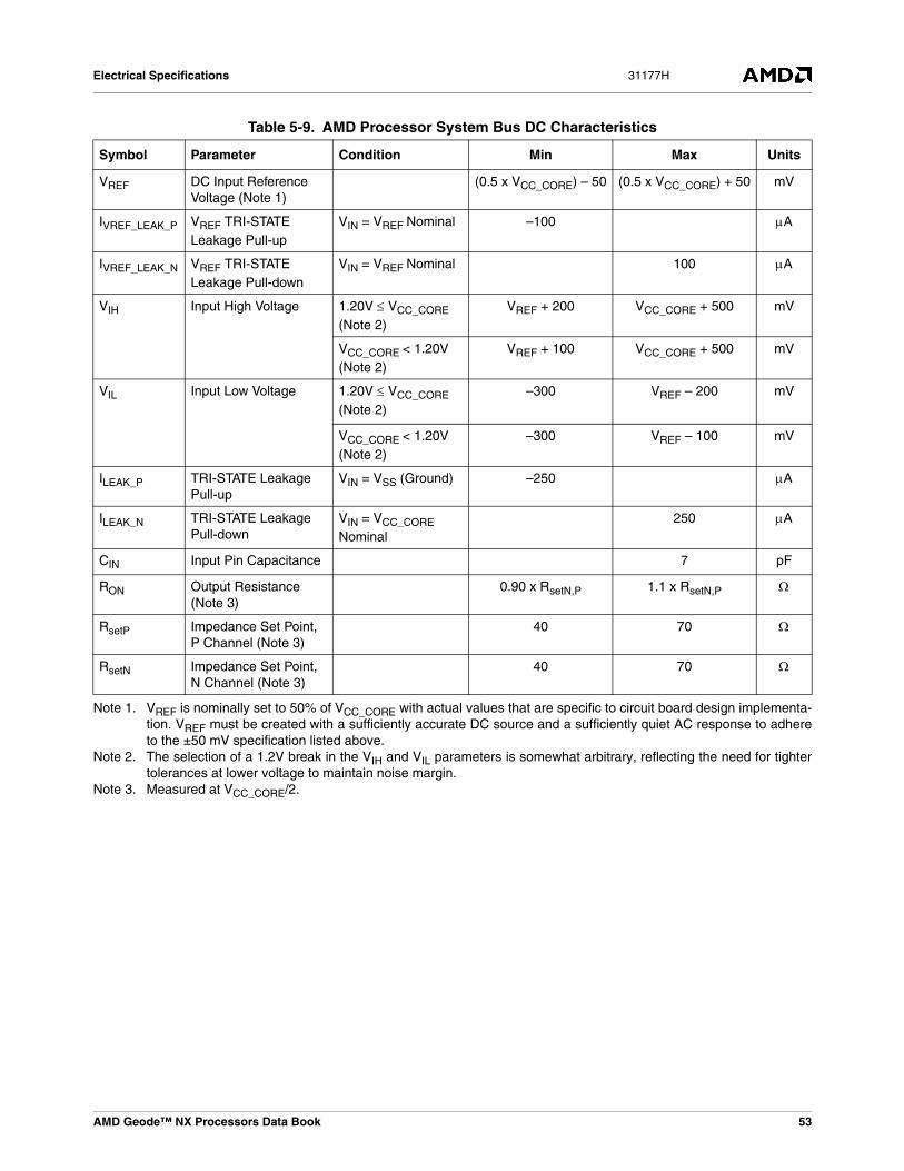
Electrical Specifications 31177H
Table 5-9. AMD Processor System Bus DC Characteristics
Symbol Parameter Condition Min Max Units
VREF DC Input Reference Voltage (Note 1)
(0.5 x VCC_CORE) – 50 (0.5 x VCC_CORE) + 50 mV
IVREF_LEAK_P VREF TRI-STATE Leakage Pull-up
VIN = VREF Nominal –100 μA
IVREF_LEAK_N VREF TRI-STATE Leakage Pull-down
VIN = VREF Nominal 100 μA
VIH Input High Voltage 1.20V ≤ VCC_CORE
(Note 2)VREF + 200 VCC_CORE + 500 mV
VCC_CORE < 1.20V (Note 2)
VREF + 100 VCC_CORE + 500 mV
VIL Input Low Voltage 1.20V ≤ VCC_CORE
(Note 2)–300 VREF – 200 mV
VCC_CORE < 1.20V (Note 2)
–300 VREF – 100 mV
ILEAK_P TRI-STATE Leakage Pull-up
VIN = VSS (Ground) –250 μA
ILEAK_N TRI-STATE Leakage Pull-down
VIN = VCC_CORE Nominal
250 μA
CIN Input Pin Capacitance 7 pF
RON Output Resistance (Note 3)
0.90 x RsetN,P 1.1 x RsetN,P Ω
RsetP Impedance Set Point, P Channel (Note 3)
40 70 Ω
RsetN Impedance Set Point, N Channel (Note 3)
40 70 Ω
Note 1. VREF is nominally set to 50% of VCC_CORE with actual values that are specific to circuit board design implementa-tion. VREF must be created with a sufficiently accurate DC source and a sufficiently quiet AC response to adhereto the ±50 mV specification listed above.
Note 2. The selection of a 1.2V break in the VIH and VIL parameters is somewhat arbitrary, reflecting the need for tightertolerances at lower voltage to maintain noise margin.
Note 3. Measured at VCC_CORE/2.
AMD Geode™ NX Processors Data Book 53

Electrical Specifications31177H
Table 5-10. General DC Characteristics
Symbol Parameter Condition Min Max Units
VIH Input High Voltage (Note 1) (Note 2) (Note 3)
1.2V ≤ VCC_CORE 0.5 x VCC_CORE + 200 VCC_CORE + 300 mV
VCC_CORE < 1.20V 0.5 x VCC_CORE + 100 VCC_CORE + 300 mV
VIL Input Low Voltage (Note 1) (Note 2) (Note 3)
1.2V ≤ VCC_CORE –300 0.5 x VCC_CORE – 200 mV
VCC_CORE < 1.20V –300 0.5 x VCC_CORE – 100 mV
VOH Output High Voltage (Note 3)
VCC_CORE – 200 VCC_CORE + 300 mV
VOL Output Low Voltage (Note 3)
–300 200 mV
ILEAK_P TRI-STATE Leakage Pull-up
VIN = VSS (Ground) –250 µA
ILEAK_N TRI-STATE Leakage Pull-down
VIN = VCC_CORE Nominal 250 µA
IOH Output High Current (Note 4)
–6 mA
IOL Output Low Current (Note 5)
6 mA
CPIN Pin Capacitance 12 pF
Note 1. Characterized across DC supply voltage range.Note 2. The selection of a 1.2V break in the VIH and VIL parameters is somewhat arbitrary, reflecting the need for tighter
tolerances at lower voltages to maintain noise margin. Note 3. Values specified at nominal VCC_CORE. Scale parameters between VCC_CORE_MIN and VCC_CORE_MAX.Note 4. IOL and IOH are measured at VOL maximum and VOH minimum, respectively.Note 5. Synchronous inputs/outputs are specified with respect to RSTCLK and RSTCK# at the pins.
54 AMD Geode™ NX Processors Data Book

Electrical Specifications 31177H
5.6 AC Characteristics
Figure 5-3 shows a sample waveform.
Figure 5-3. SYSCLK Waveform
Table 5-11. SYSCLK and SYSCLK# AC Characteristics
Symbol Parameter Min @ Max @ Units
Clock Frequency 50 133 50 133 MHz
Duty Cycle 30% 30% 70% 70%
t1 Period (Note 1) (Note 2) 10 7.5 ns
t2 High Time 1.8 1.05 ns
t3 Low Time 1.8 1.05 ns
t4 Fall Time 2 2 ns
t5 Rise Time 2 2 ns
Period Stability ± 300 ± 300 ps
Note 1. Circuitry driving the AMD processor system bus clock inputs must exhibit a suitably low closed-loop jitter bandwidthto allow the PLL to track the jitter. The –20 dB attenuation point, as measured into a 10 or 20 pF load must be lessthan 500 kHz.
Note 2. Circuitry driving the AMD processor system bus clock inputs may purposely alter the AMD processor system busclock frequency (spread spectrum clock generators). In no cases can the AMD processor system bus period violatethe minimum specification above. AMD processor system bus clock inputs can vary from 100% of the specified fre-quency to 99% of the specified frequency at a maximum rate of 100 kHz.
t5
VCROSS
t2
t3
t4
t1
VThreshold-AC
AMD Geode™ NX Processors Data Book 55

Electrical Specifications31177H
Table 5-12. PICD[1:0]# and PICCLK (APIC Pins) AC Characteristics
Symbol Parameter Min Max Units
TRISE Signal Rise Time (Note 1) 1.0 3.0 V/ns
TFALL Signal Fall Time (Note 1) 1.0 3.0 V/ns
TSU Setup Time 1 ns
THD Hold Time 1 ns
Note 1. Edge rates indicate the range for characterizing the inputs.
Table 5-13. AMD Processor System Bus AC Characteristics
Group Note 1 Symbol Parameter Min Max Units
All Signals (Note 2)
TRISE Output Rise Slew Rate 1 3 V/ns
TFALL Output Fall Slew Rate 1 3 V/ns
Forward Clocks
TSKEW-DIFFEDGE (Note 3) Output skew with respect to a dif-ferent clock edge
– 770 ps
TSU (Note 4) Input Data Setup Time 300 ps
THD (Note 4) Input Data Hold Time 300 ps
CIN Capacitance on input clocks 3 7 pF
COUT Capacitance on output clocks 4 7 pF
Sync TVAL (Note 5) (Note 6) RSTCLK to Output Valid 250 2000 ps
TSU (Note 5) (Note 7) Setup to RSTCLK 500 ps
THD (Note 5) (Note 7) Hold from RSTCLK 1000 ps
Note 1. The parameters are grouped based on the source or destination of the signals involved.Note 2. Rise and fall time ranges are guidelines over which the I/O has been characterized.Note 3. TSKEW-DIFFEDGE is the maximum skew within a clock forwarded group between any two signals or between any
signal and its forward clock, as measured at the package, with respect to different clock edges.Note 4. Input SU and HD times are with respect to the appropriate Clock Forward Group input clock.Note 5. The synchronous signals include PROCRDY, CONNECT, and CLKFWDRST.Note 6. TVAL is RSTCLK rising edge to output valid for PROCRDY. Measure the signal at the receiver end of a 50 ohm
trace. Subtract the delay effect of the transmission line.Note 7. TSU is setup of CONNECT/CLKFWDRST to rising edge of RSTCLK. THD is hold of CONNECT/CLKFWDRST from
rising edge of RSTCLK.
56 AMD Geode™ NX Processors Data Book

Electrical Specifications 31177H
Table 5-14. General AC Characteristics
Symbol Parameter Min Max Units
TSU Sync Input Setup Time (Note 1) (Note 2) 2.0 ns
THD Sync Input Hold Time (Note 1) (Note 2) 0.0 ps
TDELAY Output Delay with respect to RSTCLK (Note 2) 0.0 6.1 ns
TBIT Input Time to Acquire (Note 3) (Note 4) 20.0 ns
TRPT Input Time to Reacquire (Note 5) (Note 6) (Note 7) (Note 8) 40.0 ns
TRISE Signal Rise Time (Note 9) 1.0 3.0 V/ns
TFALL Signal Fall Time (Note 9) 1.0 3.0 V/ns
TVALID Time to Data Valid (Note 10) 100 ns
Note 1. These are aggregate numbers.Note 2. Edge rates indicate the range over which inputs were characterized.Note 3. This value assumes RSTCLK frequency is 10 ns ==> TBIT = 2 x fRST.Note 4. The approximate value for standard case in normal mode operation.Note 5. This value is dependent on RSTCLK frequency, divisors, Low Power mode, and core frequency.Note 6. Re-assertions of the signal within this time are not guaranteed to be seen by the core.Note 7. This value assumes that the skew between RSTCLK and K7CLKOUT is much less than one phase.Note 8. This value assumes RSTCLK and K7CLKOUT are running at the same frequency, though the processor is capable
of other configurations.Note 9. In asynchronous operation, the signal must persist for this time to enable capture.Note 10. Time to valid is for any open-drain pins. See requirements 7 and 8 of Section 5.10.1.1 "Signal Sequence and Timing
Description" on page 61 for more information.
AMD Geode™ NX Processors Data Book 57
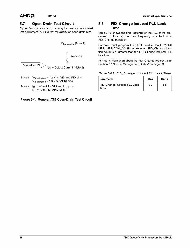
Electrical Specifications31177H
5.7 Open-Drain Test CircuitFigure 5-4 is a test circuit that may be used on automatedtest equipment (ATE) to test for validity on open-drain pins.
Figure 5-4. General ATE Open-Drain Test Circuit
5.8 FID_Change Induced PLL Lock Time
Table 5-15 shows the time required for the PLL of the pro-cessor to lock at the new frequency specified in aFID_Change transition.
Software must program the SGTC field of the FidVidCtlMSR (MSR C001_0041h) to produce a FID_Change dura-tion equal to or greater than the FID_Change induced PLLlock time.
For more information about the FID_Change protocol, seeSection 3.1 "Power Management States" on page 33.
Note 1. VTermination = 1.2 V for VID and FID pinsVTermination = 1.0 V for APIC pins
Note 2. IOL = –6 mA for VID and FID pinsIOL = –9 mA for APIC pins
IOL = Output Current (Note 2)
VTermination (Note 1)
50 Ω ±3%
Open-drain Pin
Table 5-15. FID_Change Induced PLL Lock Time
Parameter Max Units
FID_Change Induced PLL Lock Time
50 µs
58 AMD Geode™ NX Processors Data Book
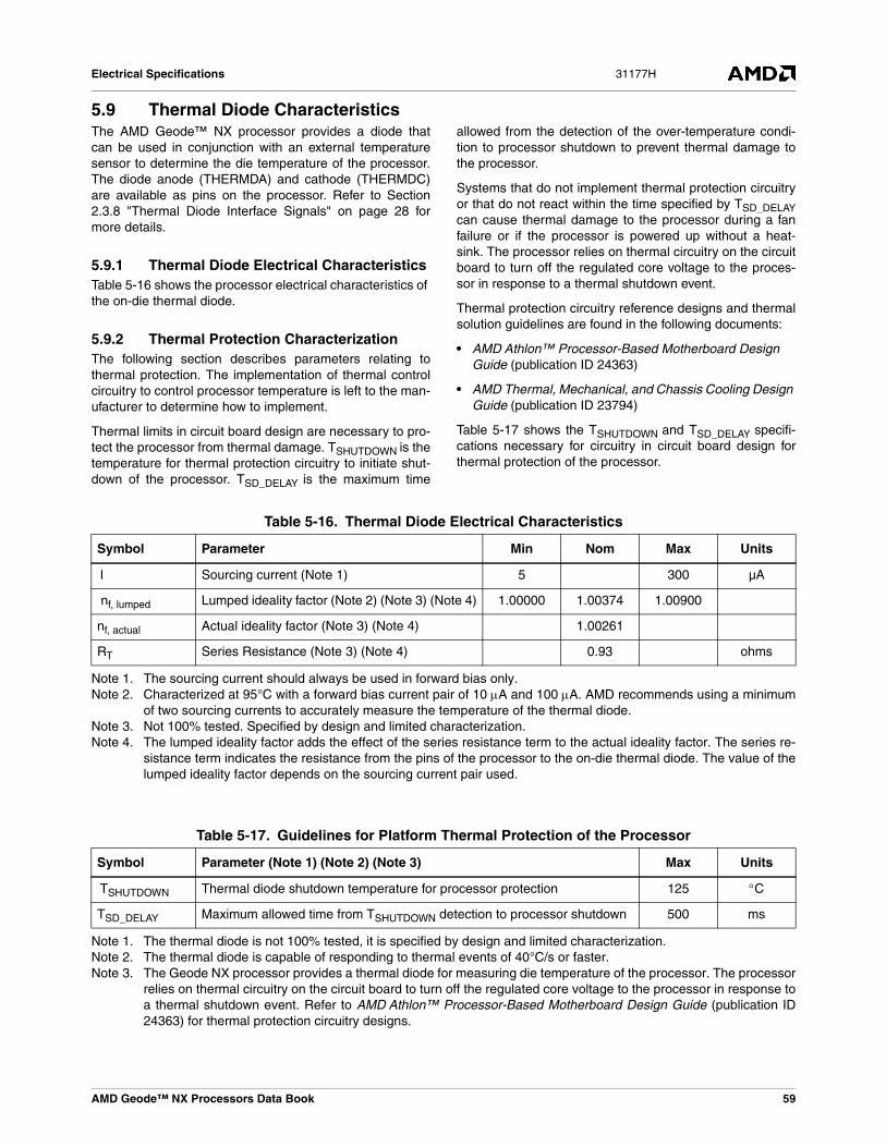
Electrical Specifications 31177H
5.9 Thermal Diode CharacteristicsThe AMD Geode™ NX processor provides a diode thatcan be used in conjunction with an external temperaturesensor to determine the die temperature of the processor.The diode anode (THERMDA) and cathode (THERMDC)are available as pins on the processor. Refer to Section2.3.8 "Thermal Diode Interface Signals" on page 28 formore details.
5.9.1 Thermal Diode Electrical CharacteristicsTable 5-16 shows the processor electrical characteristics of the on-die thermal diode.
5.9.2 Thermal Protection CharacterizationThe following section describes parameters relating tothermal protection. The implementation of thermal controlcircuitry to control processor temperature is left to the man-ufacturer to determine how to implement.
Thermal limits in circuit board design are necessary to pro-tect the processor from thermal damage. TSHUTDOWN is thetemperature for thermal protection circuitry to initiate shut-down of the processor. TSD_DELAY is the maximum time
allowed from the detection of the over-temperature condi-tion to processor shutdown to prevent thermal damage tothe processor.
Systems that do not implement thermal protection circuitryor that do not react within the time specified by TSD_DELAYcan cause thermal damage to the processor during a fanfailure or if the processor is powered up without a heat-sink. The processor relies on thermal circuitry on the circuitboard to turn off the regulated core voltage to the proces-sor in response to a thermal shutdown event.
Thermal protection circuitry reference designs and thermalsolution guidelines are found in the following documents:
• AMD Athlon™ Processor-Based Motherboard Design Guide (publication ID 24363)
• AMD Thermal, Mechanical, and Chassis Cooling Design Guide (publication ID 23794)
Table 5-17 shows the TSHUTDOWN and TSD_DELAY specifi-cations necessary for circuitry in circuit board design forthermal protection of the processor.
Table 5-16. Thermal Diode Electrical Characteristics
Symbol Parameter Min Nom Max Units
I Sourcing current (Note 1) 5 300 µA
nf, lumped Lumped ideality factor (Note 2) (Note 3) (Note 4) 1.00000 1.00374 1.00900
nf, actual Actual ideality factor (Note 3) (Note 4) 1.00261
RT Series Resistance (Note 3) (Note 4) 0.93 ohms
Note 1. The sourcing current should always be used in forward bias only. Note 2. Characterized at 95°C with a forward bias current pair of 10 μA and 100 μA. AMD recommends using a minimum
of two sourcing currents to accurately measure the temperature of the thermal diode.Note 3. Not 100% tested. Specified by design and limited characterization.Note 4. The lumped ideality factor adds the effect of the series resistance term to the actual ideality factor. The series re-
sistance term indicates the resistance from the pins of the processor to the on-die thermal diode. The value of thelumped ideality factor depends on the sourcing current pair used.
Table 5-17. Guidelines for Platform Thermal Protection of the Processor
Symbol Parameter (Note 1) (Note 2) (Note 3) Max Units
TSHUTDOWN Thermal diode shutdown temperature for processor protection 125 °C
TSD_DELAY Maximum allowed time from TSHUTDOWN detection to processor shutdown 500 ms
Note 1. The thermal diode is not 100% tested, it is specified by design and limited characterization.Note 2. The thermal diode is capable of responding to thermal events of 40°C/s or faster.Note 3. The Geode NX processor provides a thermal diode for measuring die temperature of the processor. The processor
relies on thermal circuitry on the circuit board to turn off the regulated core voltage to the processor in response toa thermal shutdown event. Refer to AMD Athlon™ Processor-Based Motherboard Design Guide (publication ID24363) for thermal protection circuitry designs.
AMD Geode™ NX Processors Data Book 59

Electrical Specifications31177H
5.9.3 Part-Specific Thermal Power Performance SpecificationsThe tables in this section specify the part-specific thermal power performance specifications for the Geode NX processor.This includes the nominal DC operating voltage of the processor core in the C0 Working state and the Stop Grant state.
Table 5-18. Thermal Power Performance Specifications
Frequency in MHzVCC_CORE
(Core Voltage)
Thermal Power Max
Maximum DieTemperature
Working State C0(Note 1)
Note 1. See Figure Figure 3-1 "Processor Power Management States" on page 33.
Stop Grant C3/S1(Note 1) (Note 2)
Note 2. Power measurements are at 500 MHz and 1.05V.The AMD processor system bus is disconnected and has a lowpower ratio of 1/64 for Stop Grant disconnect and a low power ratio of 1/64 Halt disconnect applied to the core clockgrid of the processor.
AMD Geode™ NX 1250@6W Processor (Note 3)
Note 3. The AMD Geode™ NX 1750@14W processor operates at 1.4 GHz, the NX 1500@6W processor operates at 1.0GHz, and the NX 1250@6W processor operates at 667 MHz. Model numbers reflect performance as describedhere: http://www.amd.com/connectivitysolutions/geodenxbenchmark.
667 1.10V 9.0W (Note 4) (6.0W typical)
Note 4. Thermal design power represents the maximum sustained power dissipated while executing publicly-available soft-ware or instruction sequences under normal system operation at nominal VCC_CORE. Thermal solutions must mon-itor the temperature of the processor to prevent the processor from exceeding its maximum die temperature.
3.0W 95°C
AMD Geode™ NX 1500@6W Processor (Note 3)
1000 1.00V 9.0W (Note 4) (6.0W typical)
3.0W 95°C
AMD Geode™ NX 1750@14W Processor (Note 3)
1400 1.25V 25.0W (Note 4)(14.0W typical)
3.0W 95°C
60 AMD Geode™ NX Processors Data Book

Electrical Specifications 31177H
5.10 Signal and Power-Up RequirementsThis chapter describes the AMD Geode™ NX processor’spower-up requirements during system power-up and warmresets.
5.10.1 Power-Up Requirements
5.10.1.1 Signal Sequence and Timing DescriptionFigure 5-5 shows the relationship between key signals inthe system during a power-up sequence. This figure detailsthe requirements of the processor.
Note: Figure 5-5 represents several signals genericallyby using names not necessarily consistent withany pin lists or schematics.
The signal timing requirements for Figure 5-5 are as fol-lows:
1) RESET# must be asserted before PWROK isasserted.
The Geode NX processor does not set the correctclock multiplier if PWROK is asserted prior to aRESET# assertion. It is recommended that RESET#be asserted at least 10 ns prior to the assertion ofPWROK.
In practice, a Southbridge asserts RESET# millisec-onds before PWROK is asserted.
2) All circuit board voltage planes must be within specifi-cation before PWROK is asserted.
PWROK is an output of the voltage regulation circuiton the circuit board. PWROK indicates that VCC_COREand all other voltage planes in the system are withinspecification.
The circuit board is required to delay PWROK asser-tion for a minimum of three milliseconds from the 3.3Vsupply being within specification. This delay ensuresthat the system clock (SYSCLK/SYSCLK#) is operat-ing within specification when PWROK is asserted.
The processor core voltage, VCC_CORE, must be withinspecification before PWROK is asserted as dictatedby the VID[4:0] pins strapped on the processor pack-age. Before PWROK assertion, the processor isclocked by a ring oscillator. Before PWROK isasserted, the SOFTVID[4:0] outputs of the processorare not driven to a deterministic value. The processordrives the SOFTVID[4:0] outputs to the same value asdictated by the VID[4:0] pins within 20 ns of PWROKassertion.
Figure 5-5. Signal Relationship Requirements During Power-Up Sequence
2
1
3
4
5
6
7 8
3.3 V Supply
VCCA (2.5 V)
VCC_CORE (Processor Core)
(for PLL)
RESET#
NB_RESET#
PWROK
FID[3:0]
System Clock
Warm ResetCondition
AMD Geode™ NX Processors Data Book 61
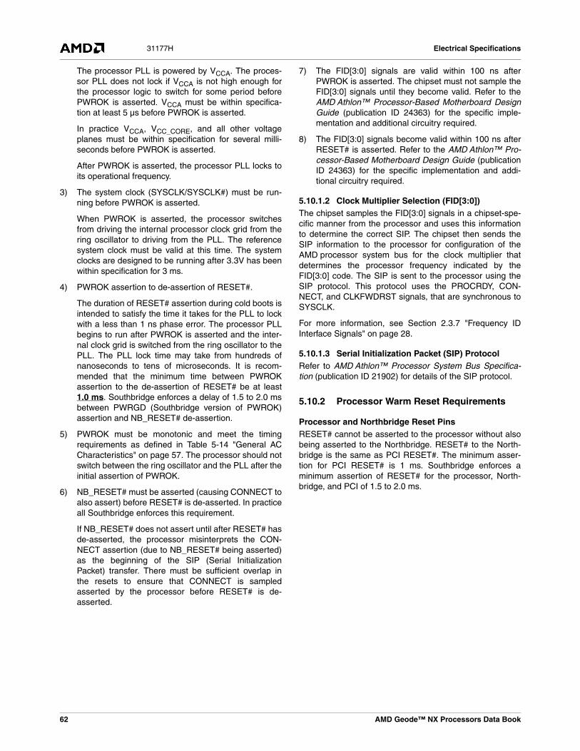
Electrical Specifications31177H
The processor PLL is powered by VCCA. The proces-sor PLL does not lock if VCCA is not high enough forthe processor logic to switch for some period beforePWROK is asserted. VCCA must be within specifica-tion at least 5 µs before PWROK is asserted.
In practice VCCA, VCC_CORE, and all other voltageplanes must be within specification for several milli-seconds before PWROK is asserted.
After PWROK is asserted, the processor PLL locks toits operational frequency.
3) The system clock (SYSCLK/SYSCLK#) must be run-ning before PWROK is asserted.
When PWROK is asserted, the processor switchesfrom driving the internal processor clock grid from thering oscillator to driving from the PLL. The referencesystem clock must be valid at this time. The systemclocks are designed to be running after 3.3V has beenwithin specification for 3 ms.
4) PWROK assertion to de-assertion of RESET#.
The duration of RESET# assertion during cold boots isintended to satisfy the time it takes for the PLL to lockwith a less than 1 ns phase error. The processor PLLbegins to run after PWROK is asserted and the inter-nal clock grid is switched from the ring oscillator to thePLL. The PLL lock time may take from hundreds ofnanoseconds to tens of microseconds. It is recom-mended that the minimum time between PWROKassertion to the de-assertion of RESET# be at least1.0 ms. Southbridge enforces a delay of 1.5 to 2.0 msbetween PWRGD (Southbridge version of PWROK)assertion and NB_RESET# de-assertion.
5) PWROK must be monotonic and meet the timingrequirements as defined in Table 5-14 "General ACCharacteristics" on page 57. The processor should notswitch between the ring oscillator and the PLL after theinitial assertion of PWROK.
6) NB_RESET# must be asserted (causing CONNECT toalso assert) before RESET# is de-asserted. In practiceall Southbridge enforces this requirement.
If NB_RESET# does not assert until after RESET# hasde-asserted, the processor misinterprets the CON-NECT assertion (due to NB_RESET# being asserted)as the beginning of the SIP (Serial InitializationPacket) transfer. There must be sufficient overlap inthe resets to ensure that CONNECT is sampledasserted by the processor before RESET# is de-asserted.
7) The FID[3:0] signals are valid within 100 ns afterPWROK is asserted. The chipset must not sample theFID[3:0] signals until they become valid. Refer to theAMD Athlon™ Processor-Based Motherboard DesignGuide (publication ID 24363) for the specific imple-mentation and additional circuitry required.
8) The FID[3:0] signals become valid within 100 ns afterRESET# is asserted. Refer to the AMD Athlon™ Pro-cessor-Based Motherboard Design Guide (publicationID 24363) for the specific implementation and addi-tional circuitry required.
5.10.1.2 Clock Multiplier Selection (FID[3:0])The chipset samples the FID[3:0] signals in a chipset-spe-cific manner from the processor and uses this informationto determine the correct SIP. The chipset then sends theSIP information to the processor for configuration of theAMD processor system bus for the clock multiplier thatdetermines the processor frequency indicated by theFID[3:0] code. The SIP is sent to the processor using theSIP protocol. This protocol uses the PROCRDY, CON-NECT, and CLKFWDRST signals, that are synchronous toSYSCLK.
For more information, see Section 2.3.7 "Frequency IDInterface Signals" on page 28.
5.10.1.3 Serial Initialization Packet (SIP) ProtocolRefer to AMD Athlon™ Processor System Bus Specifica-tion (publication ID 21902) for details of the SIP protocol.
5.10.2 Processor Warm Reset Requirements
Processor and Northbridge Reset PinsRESET# cannot be asserted to the processor without alsobeing asserted to the Northbridge. RESET# to the North-bridge is the same as PCI RESET#. The minimum asser-tion for PCI RESET# is 1 ms. Southbridge enforces aminimum assertion of RESET# for the processor, North-bridge, and PCI of 1.5 to 2.0 ms.
62 AMD Geode™ NX Processors Data Book

AMD Geode™ NX Processors Data
Mechanical Data 31177H
66.0Mechanical Data
The AMD Geode™ NX processor connects to the mother-board through a Pin Grid Array (PGA) socket namedSocket A. This processor utilizes the organic pin grid array(OPGA) package type described in this chapter. For moreinformation, see the AMD Athlon™ Processor-Based Moth-erboard Design Guide (publication ID 24363).
6.1 Die LoadingThe processor die on the OPGA package is exposed at thetop of the package. This feature facilitates heat transferfrom the die to an approved heat sink. Any heat sink designshould avoid loads on corners and edges of die. TheOPGA package has compliant pads that serve to bring sur-faces in planar contact. Tool-assisted zero insertion forcesockets should be designed so that no load is placed onthe substrate of the package.
Table 6-1 shows the mechanical loading specifications forthe processor die. It is critical that the mechanical loadingof the heat sink does not exceed the limits shown in Table6-1.
6.2 OPGA Package DescriptionsTable 6-2 shows the part number 28104 OPGA packagedimensions in millimeters assigned to the letters and sym-bols used in the package diagram, Figure 6-1 on page 64.
Table 6-1. Mechanical Loading
LocationDynamic
(Max)Static (Max) Units
Die Surface (Note 1)
Note 1. Load specified for coplanar contact to die surface.
100 30 lbf
Die Edge (Note 2)
Note 2. Load defined for a surface at no more than a two-degree angle of inclination to die surface.
10 10 lbf
Table 6-2. 28104 OPGA Package Dimensions
Letter or SymbolMin Dimension
(Note 1)Max Dimension
(Note 1) Letter or SymbolMin Dimension
(Note 1)Max Dimension
(Note 1)
D/E 49.27 49.78 G/H – 4.50
D1/E1 45.72 BSC A 1.917 REF
D2 7.47 REF A1 0.977 1.177
D3 3.30 3.60 A2 0.80 0.88
D4 10.78 11.33 A3 0.116 –
D5 10.78 11.33 A4 – 1.90
D6 8.13 8.68 φP – 6.60
D7 12.33 12.88 φb 0.43 0.50
D8 3.05 3.35 φb1 1.40 REF
D9 12.71 13.26 S 1.435 2.375
E2 11.33 REF L 3.05 3.31
E3 2.35 2.65 M 37
E4 7.87 8.42 N 453
E5 7.87 8.42 e 1.27 BSC
E6 10.73 11.28 e1 2.54 BSC
E8 13.28 13.83 Mass (Note 2) 11.0 g REF
E9 1.66 1.96
Note 1. Dimensions are given in millimeters.Note 2. The mass consists of the completed package, including processor, surface mounted parts, and pins.
Book 63
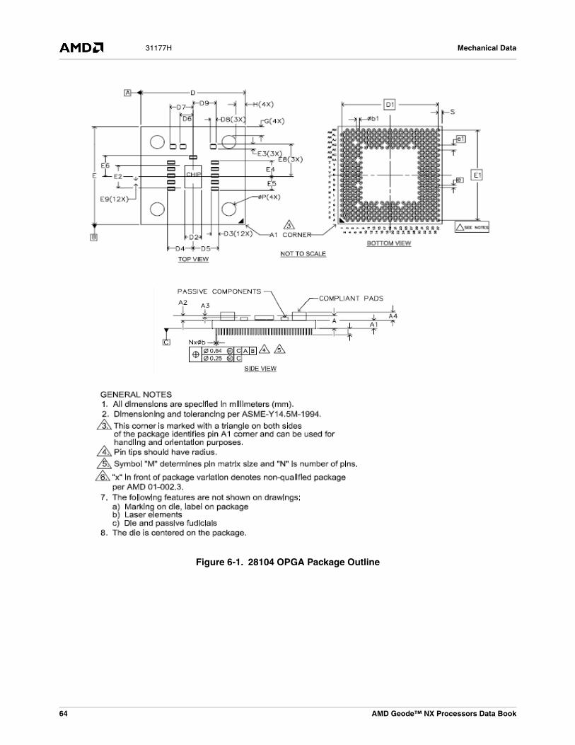
Mechanical Data31177H
Figure 6-1. 28104 OPGA Package Outline
64 AMD Geode™ NX Processors Data Book
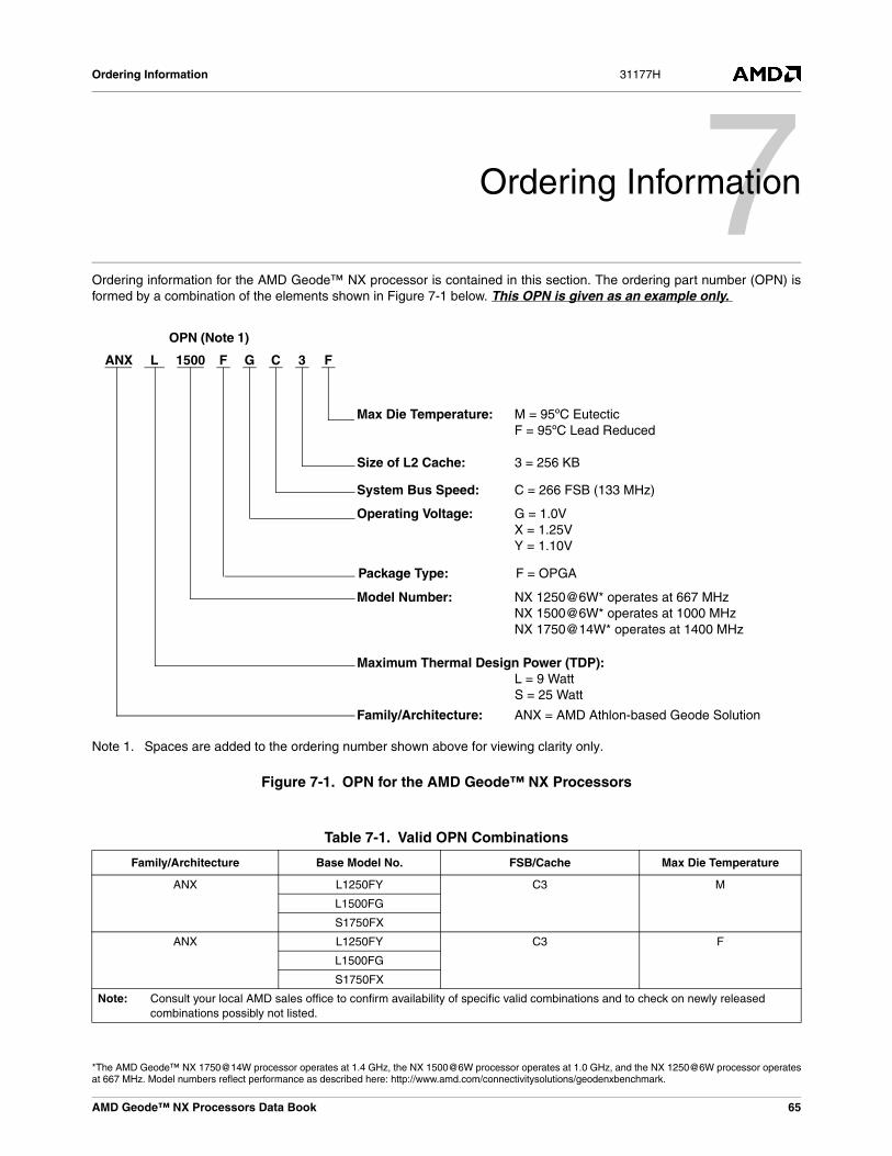
AMD Geode™ NX Processors Data
Ordering Information 31177H
*The AMD Geode™ NX 1750@14W procesat 667 MHz. Model numbers reflect perform
77.0Ordering Information
Ordering information for the AMD Geode™ NX processor is contained in this section. The ordering part number (OPN) isformed by a combination of the elements shown in Figure 7-1 below. This OPN is given as an example only.
Figure 7-1. OPN for the AMD Geode™ NX Processors
OPN (Note 1)
Family/Architecture: ANX = AMD Athlon-based Geode Solution
Model Number: NX 1250@6W* operates at 667 MHzNX 1500@6W* operates at 1000 MHzNX 1750@14W* operates at 1400 MHz
Maximum Thermal Design Power (TDP):L = 9 WattS = 25 Watt
Package Type: F = OPGA
Max Die Temperature: M = 95ºC EutecticF = 95ºC Lead Reduced
System Bus Speed: C = 266 FSB (133 MHz)
Size of L2 Cache: 3 = 256 KB
Operating Voltage: G = 1.0VX = 1.25VY = 1.10V
Note 1. Spaces are added to the ordering number shown above for viewing clarity only.
ANX L 1500 F G C 3 F
Table 7-1. Valid OPN Combinations
Family/Architecture Base Model No. FSB/Cache Max Die Temperature
ANX L1250FY C3 M
L1500FG
S1750FX
ANX L1250FY C3 F
L1500FG
S1750FX
Note: Consult your local AMD sales office to confirm availability of specific valid combinations and to check on newly released combinations possibly not listed.
Book 65
sor operates at 1.4 GHz, the NX 1500@6W processor operates at 1.0 GHz, and the NX 1250@6W processor operatesance as described here: http://www.amd.com/connectivitysolutions/geodenxbenchmark.

Ordering Information31177H
66 AMD Geode™ NX Processors Data Book
Appendix A: Thermal Diode Calculations 31177H
AAppendix ASupporting Documentation
A.1 Thermal Diode CalculationsThis section contains information about the calculations forthe on-die thermal diode of the AMD Geode™ NX proces-sor. For electrical information about this thermal diode, seeTable 5-16 "Thermal Diode Electrical Characteristics" onpage 59.
A.1.1 Ideal Diode EquationThe ideal diode equation uses the variables and constantsdefined in Table A-1.
Equation 1 shows the ideal diode calculation.
Equation 1.
Sourcing two currents and using Equation 1 derives the dif-ference in the base-to-emitter voltage that leads to findingthe diode temperature as shown in Equation 2. The use ofdual sourcing currents allows the measurement of the ther-mal diode temperature to be more accurate and less sus-ceptible to die and process revisions. Temperature sensors
that utilize series resistance cancellation can use morethan two sourcing currents and are suitable to be used withthe AMD thermal diode. Equation 2 is the formula for calcu-lating the temperature of a thermal diode.
Equation 2.
A.1.2 Temperature Offset CorrectionA temperature offset may be required to correct the valuemeasured by a temperature sensor. An offset is necessaryif a difference exists between the lumped ideality factor ofthe processor and the ideality factor assumed by the tem-perature sensor. The lumped ideality factor can be calcu-lated using the equations in this section to find thetemperature offset that should be used with the tempera-ture sensor.
Table A-2 shows the constants and variables used to calcu-late the temperature offset correction.
Table A-1. Constants and Variables for the Ideal Diode Equation
Equation Symbol Variable, Constant Description
nf, lumped Lumped ideality factor
k Boltzmann constant
q Electron charge constant
T Diode temperature (Kelvin)
VBE Voltage from base to emitter
IC Collector current
IS Saturation current
VBE nf lumped,kq--- T IC
IS
----⎝ ⎠⎛ ⎞ln⋅ ⋅ ⋅=
Table A-2. Temperature Offset Equation Constants and Variables
Equation Symbol Variable, Constant Description
nf, actual Actual ideality factor
nf, lumped Lumped ideality factor
nf, TS Ideality factor assumed by temperature sensor
Ihigh High sourcing current
Ilow Low sourcing current
Tdie, spec Die temperature specification
Toffset Temperature offset
T VBE high, VBE low,–
nf lumped,kq--- Ihigh
Ilow
--------⎝ ⎠⎛ ⎞ln⋅ ⋅
-----------------------------------------------------------------=
AMD Geode™ NX Processors Data Book 67
Appendix A: Thermal Diode Calculations31177H
The formulas in Equation 3 and Equation 4 can be used tocalculate the temperature offset for temperature sensorsthat do not employ series resistance cancellation. Theresult is added to the value measured by the temperaturesensor. Contact the vendor of the temperature sensorbeing used for the value of nf,TS. Refer to the document,On-Die Thermal Diode Characterization (publication ID25443) for further details.
Equation 3 shows the equation for calculating the lumpedideality factor (nf, lumped) in sensors that do not employseries resistance cancellation.
Equation 3.
Equation 4 shows the equation for calculating temperatureoffset (Toffset) in sensors that do not employ series resis-tance cancellation.
Equation 4.
Equation 5 is the temperature offset for temperature sen-sors that utilize series resistance cancellation. Add theresult to the value measured by the temperature sensor.Note that the value of nf,TS in Equation 5 may not equal thevalue used in Equation 4.
Equation 5.
f lumped, nf actual,= RT Ihigh Ilow–( )⋅kq--- Tdie spec, 273.15+( ) Ihigh
Ilow
--------⎝ ⎠⎛ ⎞ln⋅
--------------------------------------------------------------------------+
Toffse t
Tdie spec, 273.15+( )= 1 nf lumped,
nf TS,
----------------–⎝ ⎠⎛ ⎞⋅
Toffset
Tdie spec, 273.15+( )= 1 nf actual,
nf TS,
----------------–⎝ ⎠⎛ ⎞⋅
68 AMD Geode™ NX Processors Data Book
Appendix A: Conventions, Abbreviations, and References 31177H
A.2 Conventions, Abbreviations, and ReferencesThis section contains information about the conventionsand abbreviations used in this document.
A.2.1 Signals and Bits
• Active-Low Signals—Signal names containing a pound sign, such as SFILLVALID#, indicate active-Low signals. They are asserted in their Low-voltage state and negated in their High-voltage state. When used in this context, High and Low are written with an initial upper case letter.
• Signal Ranges—In a range of signals, the highest and lowest signal numbers are contained in brackets and separated by a colon (for example, D[63:0]).
• Reserved Bits and Signals—Signals or bus bits marked reserved must be driven inactive or left unconnected, as indicated in the signal descriptions. These bits and signals are reserved by AMD for future implementations. When software reads registers with reserved bits, the reserved bits must be masked. When software writes such registers, it must first read the register and change only the non-reserved bits before writing back to the register.
• Three-State—In timing diagrams, signal ranges that are high impedance are shown as a straight horizontal line half-way between the high and low levels.
• Invalid and Don’t-Care—In timing diagrams, signal ranges that are invalid or don't-care are filled with a screen pattern.
A.2.2 Data TerminologyThe following list defines data terminology:
• Quantities— A word is two bytes (16 bits)— A doubleword is four bytes (32 bits)— A quadword is eight bytes (64 bits)— An octaword is 16 bytes (128 bits)— A cache line is eight quadwords (64 bytes)
• Addressing—Memory is addressed as a series of bytes on 8-byte (64-bit) boundaries in which each byte can be separately enabled.
• Abbreviations—The following notation is used for bits and bytes: — Kilo (K, as in 4-Kbyte page)— Mega (M, as in 4 Mbits/sec)— Giga (G, as in 4 Gbytes of memory space)
See Table A-3 for more abbreviations.
• Little-Endian Convention—The byte with the address xx...xx00 is in the least-significant byte position (little end). In byte diagrams, bit positions are numbered from right to left—the little end is on the right and the big end is on the left. Data structure diagrams in memory show low addresses at the bottom and high addresses at the top. When data items are aligned, bit notation on a 64-bit
data bus maps directly to bit notation in 64-bit-wide memory. Because byte addresses increase from right to left, strings appear in reverse order when illustrated.
• Bit Ranges—In text, bit ranges are shown with brackets and a colon (for example, bits [9:1]). The same applies for signal or bus names. The highest and lowest bit numbers are contained in brackets and separated by a colon (for example, AD[31:0]).
• Bit Values—Bits can either be set to 1 or cleared to 0.
• Hexadecimal and Binary Numbers—Unless the context makes interpretation clear, hexadecimal numbers are followed by an h and binary numbers are followed by a b.
A.2.3 Abbreviations and AcronymsTable A-3 contains the definitions of abbreviations used inthis document.
Table A-3. Definitions of Abbreviations
Abbreviation Meaning
A Ampere
F Farad
G Giga–
Gb Gigabit
GB Gigabyte
H Henry
h Hexadecimal
K Kilo–
KB Kilobyte
M Mega–
Mb Megabit
MB Megabyte
MHz Megahertz
m Milli–
ms Millisecond
mW Milliwatt
µ Micro–
µA Microampere
µF Microfarad
µs Microsecond
µV Microvolt
n nano–
nA nanoampere
ns nanosecond
ohm Ohm
p pico–
pF picofarad
pH picohenry
ps picosecond
s Second
V Volt
W Watt
AMD Geode™ NX Processors Data Book 69
Appendix A: Conventions, Abbreviations, and References31177H
Table A-4 contains the definitions of acronyms that mayhave been used in this document.
A.2.4 Web Sites and Support
• www.amd.com
Other web sites of interest include the following:• JEDEC home page—www.jedec.org• IEEE home page—www.computer.org• AGP Forum—www.agpforum.org
Table A-4. Definitions of Acronyms
Acronyms Meaning
ACPI Advanced Configuration and Power Interface
AGP Accelerated Graphics Port
APCI AGP Peripheral Component Interconnect
API Application Programming Interface
APIC Advanced Programmable Interrupt Controller
BIOS Basic Input/Output System
BIST Built-In Self-Test
BIU Bus Interface Unit
CPGA Ceramic Pin Grid Array
DDR Double-Data Rate
DIMM Dual Inline Memory Module
DMA Direct Memory Access
DRAM Direct Random Access Memory
EIDE Enhanced Integrated Device Electronics
EISA Extended Industry Standard Architecture
EPROM Enhanced Programmable Read Only Memory
FIFO First In, First Out
FSB Front Side Bus
GART Graphics Address Remapping Table
HSTL High-Speed Transistor Logic
IDE Integrated Device Electronics
ISA Industry Standard Architecture
JEDEC Joint Electron Device Engineering Council
JTAG Joint Test Action Group
LAN Large Area Network
LRU Least-Recently Used
LVTTL Low Voltage Transistor to Transistor Logic
MSB Most Significant Bit
MUX Multiplexer
NMI Non-Maskable Interrupt
OD Open-drain
OPGA Organic Pin Grid Array
PGA Pin Grid Array
PA Physical Address
PCI Peripheral Component Interconnect
PDE Page Directory Entry
PDT Page Directory Table
PLL Phase Locked Loop
PMSM Power Management State Machine
POS Power-On Suspend
POST Power-On Self-Test
RAM Random Access Memory
ROM Read Only Memory
RXA Read Acknowledge Queue
SDI System DRAM Interface
SDRAM Synchronous Direct Random Access Memory
SIP Serial Initialization Packet
SMbus System Management Bus
SPD Serial Presence Detect
SRAM Synchronous Random Access Memory
SROM Serial Read Only Memory
TLB Translation Lookaside Buffer
TOM Top of Memory
TTL Transistor to Transistor Logic
VAS Virtual Address Space
VPA Virtual Page Address
VGA Video Graphics Adapter
USB Universal Serial Bus
ZDB Zero Delay Buffer
Acronyms Meaning
70 AMD Geode™ NX Processors Data Book
Appendix A: Revision History 31177H
A.3 Revision HistoryThis document is a report of the revision/creation process of the data book for the AMD Geode™ NX processor. Any revi-sions (i.e., additions, deletions, parameter corrections, etc.) are recorded in the table(s) below.
Table A-5. Revision History
Date Revision Description
May 2004 A Initial release
September 2004 B See revision B for details.
October 2004 C Removed “Preliminary” label and changed “LeadFree” to “Lead Reduced”
March 2005 D Corrected information in notes for Tables 6-2 and 8-2 concerning minimum voltage.
June 2005 E Major addition was adding APIC interface. See revision E for details.
September 2005 F Big re-write / organizational layout changes. See revision F for details.
March 2006 G Updated mechanical data section with 28104 OPGA package dimensions and incor-porated other minor edits.
April 2006 H Updated Section 7.0 "Ordering Information" on page 65 with three new OPNs: ANXL1250FYC3F, ANXL1500FGC3F, and ANXS1750FXC3F. An F in the last char-acter of the order number means 95ºC Lead Reduced.
AMD Geode™ NX Processors Data Book 71

One AMD Place • P.O. Box 3453 • Sunnyvale, CA 94088-3453 USA • Tel: 408-749-4000 or 800-538-8450 • TWX: 910-339-9280 • TELEX: 34-6306
www.amd.com