ame synchronous boost converter with low quie scent current · 2013-09-10 · ame 1 ame5177 rev....
TRANSCRIPT

AME
1
AME5177
Rev. A.01
Synchronous Boost ConverterWith Low Quiescent Current
n Typical Application
n Functional Block Diagram
n General Description
The AME5177 is a high efficiency synchronous boostconverter, which is based on a hysteretic controller topol-ogy using synchronous rectification to obtain maximumefficiency at minimal quiescent currents. The converterprovides a power supply solution for products poweredby a variety of batteries such as single-cell, dual-cell,tree-cell alkaline, NiCd or NiMH, or one-cell Li-Ion or Li-polymer battery.
The output voltage is internally programmable in a rangefrom 1.8V to 5V in increments of 0.1V. Moreover, theconverter can be switched off by an enable pin to mini-mize battery drain. The maximum average input currentis limited to 450mA for current limit.
n Features
±
n Applicationl All One-Cell, Two-Cell and Three-Cell Alkaline,
NiCd, NimH and Single-Cell Batteriesl Wireless Mousel Mobile-Applicationsl Hand-Held Devices
l Very Low Start-up Voltage at 0.8Vl Output Voltage Range: 1.8V~5V in 0.1V
incrementsl Output Voltage Accuracy 2%l Output Currents up to 100mAl No Schottky Diode Requiredl Support Inductor of Multilayer Typel Typical Shutdown Current Less than 0.7uAl Typical Quiescent Current Less than 6.5uAl Over Current Protectionl Over Temperature Protectionl Available in SOT-25, SOT-26 and DFN-6D
Packagel RoHS Compliant and Halogen Free

AME
2
AME5177
Rev. A.01
Synchronous Boost ConverterWith Low Quiescent Current
n Pin Configuration
SOT-25Top View
n Pin Description
SOT-26Top View
DFN-6D(2mmx2mmx0.75mm)
Top View
6
5
4
1
2
3
AME5177-AVYxxx1. NC2. GND3. EN4. OUT5. NC6. LX
* Die Attach: Conductive Epoxy
SOT-26Top View
AME5177-BEYxxx1. LX2. GND3. EN4. NC5. VOUT6. NC
* Die Attach: Conductive Epoxy
AME5177-AEVxxx1. NC2. GND3. EN4. OUT5. LX
* Die Attach: Conductive Epoxy
AME5177-AEYxxx1. NC2. NC3. GND4. OUT5. LX6. EN
* Die Attach: Non-Conductive Epoxy
1 32
5 4
AME5177
1 32
6 45
AME5177
1 32
6 45
AME5177
A B
1 1, 2 4, 6 1, 5 NC No connect Pin.
2 3 2 2 GND Ground.
3 6 3 3 EN Chip Enable (Active High).
4 4 5 4 OUT Output Voltage Pin.
5 5 1 6 LX Switch pin which connected to inductor.
Pin Name Pin Description
Pin No.
SOT-25 DFNSOT-26

AME
3
AME5177
Rev. A.01
Synchronous Boost ConverterWith Low Quiescent Current
n Ordering Information
Number of Pins
Package Type
Pin Configuration
AME5177 - x x x xxx
Output Voltage
A 1. NC E: SOT-2X V: 5 180: 1.8V(DFN-6D) 2. GND V: DFN Y: 6 190: 1.9V
3. EN 200: 2.0V4. OUT : :5. NC : :6. LX 490: 4.9V
500: 5.0VA 1. NC
(SOT-25) 2. GND3. EN4. OUT5. LX
A 1. NC(SOT-26) 2. NC
3. GND4. OUT5. LX6. EN
B 1. LX(SOT-26) 2. GND
3. EN4. NC5. VOUT6. NC
Pin Configuration Package Type Number of Pins Output Voltage

AME
4
AME5177
Rev. A.01
Synchronous Boost ConverterWith Low Quiescent Current
n Absolute Maximum Ratings
n Recommended Operating Conditions
Maximum Unit
-0.3V to 7 V
-0.3V to 7 V
-0.3V to 7 V
-0.3V to 7 V
2000 V
200 V
1000 V
150 oC
-65 to +150 oCStorage Temperature
Input Voltage
Parameter
Electrostatic Discharge (MM)
Electrostatic Discharge (CDM)
LX Voltage
Output Voltage
EN Voltage
Electrostatic Discharge (HBM)
Junction Temperature
Parameter Symbol Rating Unit
Input Voltage VIN 0.8 to 5.5
Output Voltage VOUT 1.8 to 5
Junction Temperature Range TJ -40 to +125
Ambient Temperature Range TA -40 to +85
oC
V

AME
5
AME5177
Rev. A.01
Synchronous Boost ConverterWith Low Quiescent Current
n Thermal Information
* Measure θJC on backside center of molding compound if IC has no tab.** MIL-STD-202G 210F
Parameter Package Die Attach Symbol Maximum Unit
Thermal Resistance*(Junction to Case) θJC TBD
Thermal Resistance(Junction to Ambient) θJA TBD
Internal Power Dissipation PD TBD mW
260 oC
Non-Conductive EpoxyoC / W
Lead Temperature ( soldering 10 sec)**
SOT-25SOT-26DFN-6D

AME
6
AME5177
Rev. A.01
Synchronous Boost ConverterWith Low Quiescent Current
n Electrical Specifications
TA = 25oC, unless otherwise noted.
Parameter Symbol Test Condition Min Typ Max Units
Minimum Input VoltageAt Startup
VSTART-UP IOUT=1mA, VIN:02V 0.8 0.95 V
Hold-on Voltage(V) VHOLD IOUT=1mA, VIN:2V0V 0.7 V
Output Accuracy ∆VOUT -2 2 %
VOUT=1.8V 1.8 V
VOUT=2.1V 2.1 V
VOUT=2.2V 2.2 V
VOUT=2.7V 2.7 V
VOUT=3.0V 3 V
VOUT=3.3V 3.3 V
VOUT=5.0V 5 V
Quiescent Current IQ VOUT x 1.2 6.5 10 µA
Rectifying Switch on Resistance RDS(ON)_P VOUT=3.3V 1 Ω
Main Switch on Resistance RDS(ON)_N VOUT=3.3V 1 Ω
EN Logic-High Voltage VIH 0.8 V
EN Logic-Low Voltage VIL 0.4 V
EN Input Current IEN Clamp on GND or VOUT 0.1 1 µA
Shutdown Current ISDVEN=0V, VIN=1.2V
IOUT=0mA0.7 µA
Switch Current Limit ISW VOUT=3.3V 450 mA
NMOS Leakage Ileakage_N VOUT=3.3V 1 µA
PMOS Leakage Ileakage_P VOUT=3.3V 1 µA
Thermal Shutdown Temperature TSD 150 oC
Thermal Shutdown Hysteresis ∆TSD 20 oC
DC/DC Stage
Protection
Enable Control (SOT-25 Only)
Output Voltage ∆VOUT
Power MOSFET

AME
7
AME5177
Rev. A.01
Synchronous Boost ConverterWith Low Quiescent Current
The AME5177 is a high efficiency synchronous boostconverter, which is based on a hysteretic current control-ler topology using synchronous rectification to obtainmaximum efficiency at minimal quiescent current condi-tion. The converter allows the use of low cost chip induc-tor (Support Inductor of Multilayer Type) and small ce-ramic input and output capacitors total only three exter-nal components.
Enable Function
The AME5177 has a dedicated enable pin. The deviceis enabled when pull the EN above 0.8V. Furthermore,the device is disabled when pull the EN below 0.4V.
Over Current Limit
The AME5177 provide the current limit protection func-tion. When inductor current reaches the internal switchcurrent limit threshold, the internal switch will be turnedoff. When the over current state is eliminated, the ICresumes its nornal operation.
Over Temperature Protection
When the junction temperature exceeds 150oC, the overtemperature protection circuit turns off the internal switch,the converter will not turn back on until the device hascooled approximately 20 degrees. For normal operation,the junction temperature cannot exceed TJ=+125oC.
n Detailed Description n Application InformationInductor
The Inductor is required to supply energy to the loadwhile being driven by switched high side MOSFET.Choose inductance that will affect the period proportionalto inductance. Therefore, choosing greater inductancecan improve system efficiency since the switching fre-quency is decreased to reduce system switching losses.Finally, the choice of which style inductor to utilize mainlydepends on the price vs. size requirements and any EMIconstraints. Suggesting the inductance range is from10µH to 33µH.
Input Capacitor
Use low ESR capacitors for the best performance.When using ceramic capacitors make sure that they haveenough capacitance to provide sufficient charge to pre-vent excessive voltage ripple at input terminal. Further-more, an input capacitor improves EMI problems in thepower supply circuit.
Output Capacitor
The output capacitor is required to place enough ca-pacitance to improve the system efficiency and outputripple. Ceramic capacitors are recommended. Low ESRcapacitors are preferred to keep the output voltage ripplelow. Furthermore, the output capacitance can be esti-mated by:
Where L is the inductance. The characteristics of theoutput capacitor also affect the stability transient behav-ior of the regulation system. The AME5177 can be opti-mized for a wide range of capacitance and ESR values,such as solid tantalum, ceramic, and aluminum electro-lytic capacitors.
2L
COUT ≥

AME
8
AME5177
Rev. A.01
Synchronous Boost ConverterWith Low Quiescent Current
Layout Considerations
PCB Layout is important to achieve stable operation for switching power system at the high switching frequenciesand high peak currents conditions. For best results, follow these guidelines:
(1) The input capacitor placed as close and wide as possible to VIN and GND pins of the IC is recommended.
(2) The output capacitor placed as close and wide as possible to VOUT and GND pins of the IC is recommended.
(3) Place Lx Pin as short and wide to the IC as possible.
Table 1. List of Components
Typical Application Circuit
Component Reference Manufacturer Part Number Value
C1 Murata GRM188R60JA106ME47 10µF, 6.3V, X5R
C2 Murata GRM188R60JA106ME47 10µF, 6.3V, X5R
L1 Murata LQH43PN100M26 10µH
VIN VOUTLX OUT
EN GNDC210µF
L1 10µH
C110µF

AME
9
AME5177
Rev. A.01
Synchronous Boost ConverterWith Low Quiescent Current
Efficiency vs. Output Current
CCM Output Voltage Ripple
Quiescent Current vs. Temperature
n Characterization Curve
DCM Output Voltage Ripple
Output Voltage vs. Temperature
Power ON from Input Voltage
Output Current (A)
Effi
cien
cy (%
)
2.0µs/Div
C2
C4
VOUT(20mV/Div)
C3
IL(50mA/Div)
0.0
10.0
20.0
30.0
40.0
50.0
60.0
70.0
80.0
90.0
100.0
0.00010 0.00100 0.01000 0.10000
VIN=1.5V , VOUT=2.7V , L=10µH
2.0µs/Div
C2
C4
VOUT(20mV/Div)
IL(50mA/Div)
2.55
2.60
2.65
2.70
2.75
2.80
-50 -25 0 25 50 75 100 125
VOUT=2.7V
Temperature (oC)
Out
put V
olta
ge (V
)
3
3.5
4
4.5
5
5.5
6
6.5
-50 -25 0 25 50 75 100 125
VOUT=2.1V
Temperature (oC)Q
uies
cent
Cur
rent
(uA
)
2.0ms/Div
C4
C2VOUT
(1V/Div)
IL(100mA/Div)
VIN(1V/Div)

AME
10
AME5177
Rev. A.01
Synchronous Boost ConverterWith Low Quiescent Current
n Tape and Reel Dimension
SOT-25
Carrier Tape, Number of Components Per Reel and Reel Size
SOT-26
Package Carrier Width (W) Pitch (P) Part Per Full Reel Reel Size
SOT-25 8.0±0.1 mm 4.0±0.1 mm 3000pcs 180±1 mm
Carrier Tape, Number of Components Per Reel and Reel Size
W
P
AME AME
PIN 1
PIN 1
W
P
AME AME
Package Carrier Width (W) Pitch (P) Part Per Full Reel Reel Size
SOT-26 8.0±0.1 mm 4.0±0.1 mm 3000pcs 180±1 mm

AME
11
AME5177
Rev. A.01
Synchronous Boost ConverterWith Low Quiescent Current
n Tape and Reel Dimension (Contd.)
Carrier Tape, Number of Components Per Reel and Reel Size
DFN-6D(2mmx2mmx0.75mm)
W
P
PIN 1
AM
E
AM
E
Package Carrier Width (W) Pitch (P) Part Per Full Reel Reel Size
DFN-6D(2x2x0.75mm) 8.0±0.1 mm 4.0±0.1 mm 3000pcs 180±1 mm
AME
12
AME5177
Rev. A.01
Synchronous Boost ConverterWith Low Quiescent Current
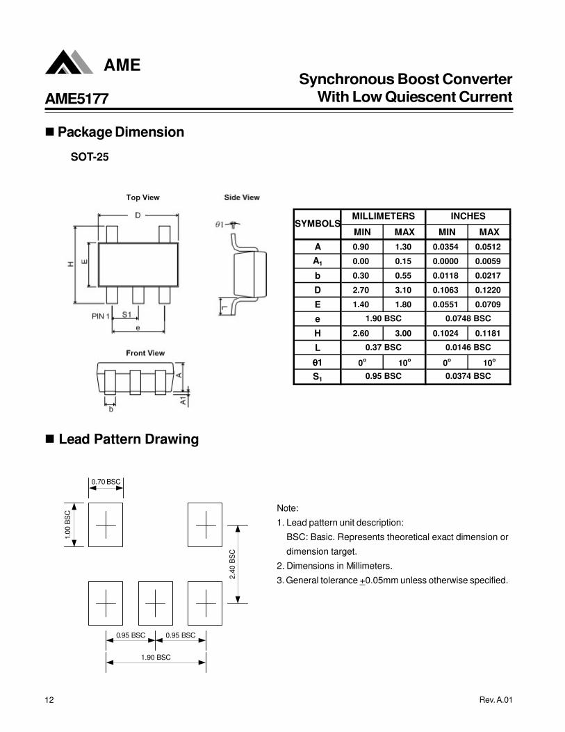
n Package Dimension
SOT-25
MIN MAX MIN MAX
A 0.90 1.30 0.0354 0.0512
A1 0.00 0.15 0.0000 0.0059
b 0.30 0.55 0.0118 0.0217
D 2.70 3.10 0.1063 0.1220
E 1.40 1.80 0.0551 0.0709
eH 2.60 3.00 0.1024 0.1181
L
θθθθ1 0o 10o 0o 10o
S1 0.95 BSC 0.0374 BSC
SYMBOLSMILLIMETERS INCHES
1.90 BSC 0.0748 BSC
0.37 BSC 0.0146 BSC
n Lead Pattern Drawing
0.70 BSC
1.00
BS
C
0.95 BSC 0.95 BSC
1.90 BSC
2.40
BS
C
Note:
1. Lead pattern unit description:
BSC: Basic. Represents theoretical exact dimension or
dimension target.
2. Dimensions in Millimeters.
3. General tolerance +0.05mm unless otherwise specified.

AME
13
AME5177
Rev. A.01
Synchronous Boost ConverterWith Low Quiescent Current
n Package Dimension (Contd.)
Side View
L
Top View
S1
De
EH
Front View
b
AA
1
PIN 1
SOT-26
TOP VIEW BOTTOM VIEW
REAR VIEW
eD
E
A GG1
b L
E1
D1
PIN 1 IDENTIFICATION
DFN-6D(2mmx2mmx0.75mm)
MIN MAX MIN MAXA 0.700 0.800 0.028 0.031
D 1.900 2.100 0.075 0.083
E 1.900 2.100 0.075 0.083
eD1 1.100 1.650 0.043 0.065
E1 0.600 1.050 0.024 0.041
b 0.180 0.350 0.007 0.014
L 0.200 0.450 0.008 0.018
G 0.178 0.228 0.007 0.009
G1 0.000 0.050 0.000 0.002
SYMBOLSMILLIMETERS INCHES
0.650 TYP 0.026 TYP

Life Support Policy:These products of AME, Inc. are not authorized for use as critical components in life-support
devices or systems, without the express written approval of the presidentof AME, Inc.
AME, Inc. reserves the right to make changes in the circuitry and specifications of its devices andadvises its customers to obtain the latest version of relevant information.
AME, Inc. , June 2013Document: A015A-DS5177-A.01
Corporate HeadquarterAME, Inc.8F, 12, WenHu St., Nei-HuTaipei 114, Taiwan .Tel: 886 2 2627-8687Fax: 886 2 2659-2989
www.ame.com.twE-Mail: [email protected]