american national standard for vpx baseline standard · ansi/vita 46.0-2007 american national...
TRANSCRIPT

ANSI/VITA 46.0-2007
American National Standard
for VPX Baseline Standard
Secretariat VMEbus International Trade Association Approved October 2007 American National Standards Institute, Inc.
VMEbus International Trade Association PO Box 19658, Fountain Hills, AZ 85269
PH: 480-837-7486, FAX: Contact VITA Office E-mail: [email protected], URL: http://www.vita.com
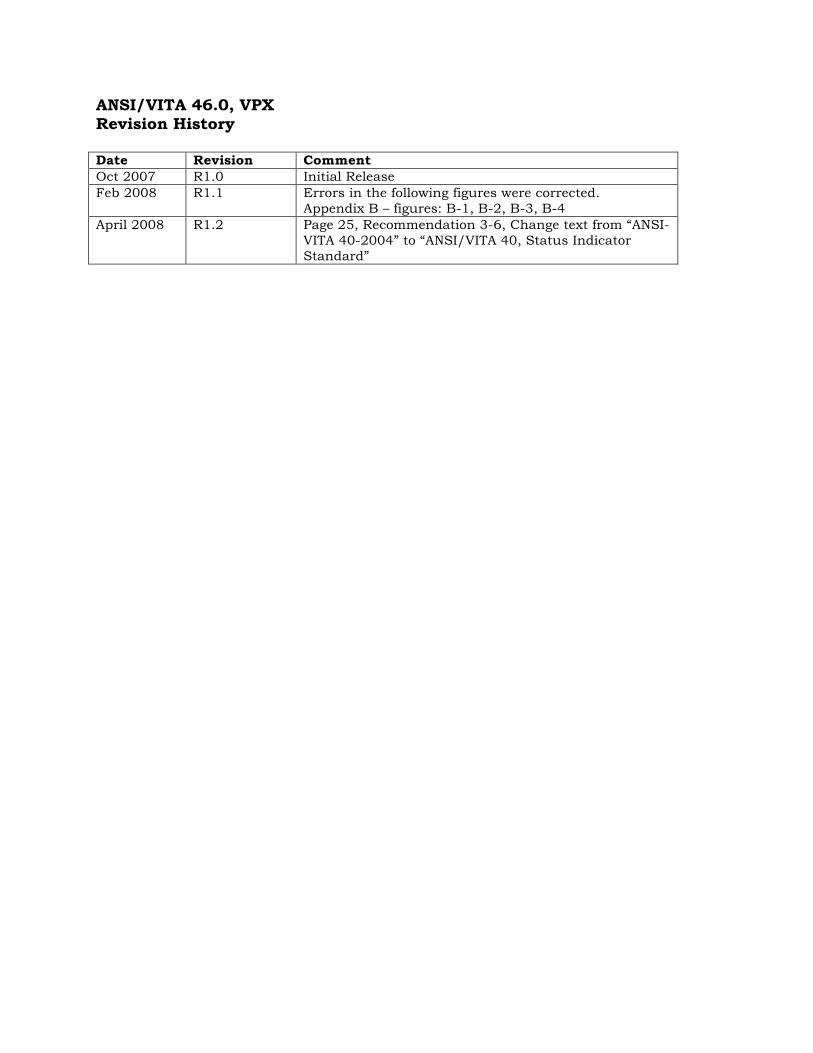
ANSI/VITA 46.0, VPX Revision History Date Revision Comment Oct 2007 R1.0 Initial Release Feb 2008 R1.1 Errors in the following figures were corrected.
Appendix B – figures: B-1, B-2, B-3, B-4 April 2008 R1.2 Page 25, Recommendation 3-6, Change text from “ANSI-
VITA 40-2004” to “ANSI/VITA 40, Status Indicator Standard”

ANSI/VITA 46.0-2007
American National Standard
for VPX Baseline Standard
Secretariat VMEbus International Trade Association Approved October 2007 American National Standards Institute, Inc. Abstract This standard describes VITA 46.0 VPX Baseline Standard, an evolutionary step forward for the provision of high-speed interconnects in harsh environment applications.

American National Standard
Approval of an American National Standard requires verification by ANSI that the requirements for due process, consensus, and other criteria for approval have been met by the standards developer. Consensus is established when, in the judgment of the ANSI Board of Standards Review, substantial agreement has been reached by directly and materially affected interests. Substantial agreement means much more than a simple majority, but not necessarily unanimity. Consensus requires that all views and objections be considered, and that a concerted effort be made toward their resolution. The use of American National Standards is completely voluntary; their existence does not in any respect preclude anyone, whether he has approved the standards or not, from manufacturing, marketing, purchasing, or using products, processes, or procedures not conforming to the standards. The American National Standards Institute does not develop standards and will in no circumstances give an interpretation of any American National Standard. Moreover, no person shall have the right or authority to issue an interpretation of an American National Standard in the name of the American National Standard Institute. Requests for interpretations should be addressed to the secretariat or sponsor whose name appears on the title page of this standard. CAUTION NOTICE: This American National Standard may be revised or withdrawn at any time. The procedures of the American National Standards Institute require that action be taken periodically to reaffirm, revise, or withdraw this standard. Purchases of American National Standards may receive current information on all standard by calling or writing the American National Standards Institute.
NOTE – The user’s attention is called to the possibility that compliance with this standard may require use of an invention covered by patent rights. By publication of this standard, no position is taken with respect to the validity of this claim or of any patent rights in connection therewith. The patent holder has, however, filed a statement of willingness to grant a license under these rights on reasonable and nondiscriminatory terms and conditions to applicants desiring to obtain such a license. Details may be obtained from the standards developer. Published by
VMEbus International Trade Association PO Box 19658, Fountain Hills, AZ 85269 Copyright © 2007 by VMEbus International Trade Association All rights reserved. No part of this publication may be reproduced in any form, in an electronic retrieval system or otherwise, without prior written permission of the publisher. Printed in the United States of America - R1.2, ISBN 1-885731-44-2

ANSI/VITA 46.0, VPX Baseline Standard
Page 2
Table of Contents
1 INTRODUCTION.....................................................................................................12
1.1 Objectives...................................................................................................................................................... 12
1.2 VITA 46 Overview ....................................................................................................................................... 12
1.3 Terminology.................................................................................................................................................. 14 1.3.1 Specification Key Words .......................................................................................................................... 14 1.3.2 VITA 46 Definitions ................................................................................................................................. 15
1.4 References..................................................................................................................................................... 16
2 VITA 46 COMPLIANCE..........................................................................................18
3 SYSTEM .................................................................................................................19
3.1 Safety Ground .............................................................................................................................................. 19
3.2 Power Supply................................................................................................................................................ 20 3.2.1 Capacity .................................................................................................................................................... 20 3.2.2 Voltage Levels .......................................................................................................................................... 20 3.2.3 Dielectric Separation................................................................................................................................. 23
3.3 System Controller (SYS_CON) .................................................................................................................. 23
3.4 System-wide Connections............................................................................................................................ 23 3.4.1 Reference Clock (REF_CLK+/-) .............................................................................................................. 23 3.4.2 JTAG Pin Allocation................................................................................................................................. 24 3.4.3 System Management Connections (Optional) .......................................................................................... 25 3.4.4 Non-Volatile Memory Read Only (Optional) ........................................................................................... 25 3.4.5 SYSRESET* ............................................................................................................................................. 25
3.5 Status Indicators .......................................................................................................................................... 25
3.6 Slot Type Indication..................................................................................................................................... 26
4 COMMON REQUIREMENTS .................................................................................27
4.1 Overview ....................................................................................................................................................... 27
4.2 Connectors .................................................................................................................................................... 27
4.3 Form Factor and Outline ............................................................................................................................ 29
4.4 Alignment and Keying................................................................................................................................. 29 4.4.1 Background and Assumptions .................................................................................................................. 29 4.4.2 Definitions................................................................................................................................................. 31 4.4.3 Keying Rules............................................................................................................................................. 31

ANSI/VITA 46.0, VPX Baseline Standard
Page 3
4.5 Two Level Maintenance (Optional)............................................................................................................ 33
4.6 Connector Pin Definition - P0..................................................................................................................... 33
4.7 Electrical Budgets for Protocol Standards ................................................................................................ 34
4.8 Signal Definition – P0 .................................................................................................................................. 36 4.8.1 Power ........................................................................................................................................................ 36 4.8.2 Geographical Addressing .......................................................................................................................... 38 4.8.3 System Controller (SYS_CON) ................................................................................................................ 39 4.8.4 Reference Clock (Optional) ...................................................................................................................... 39 4.8.5 Non-Volatile Memory Read Only (Optional) ........................................................................................... 40 4.8.6 Reserved for Future Use Differential Pair ................................................................................................ 41 4.8.7 JTAG Pin Allocation (Optional) ............................................................................................................... 41 4.8.8 System Management Connections (Optional) .......................................................................................... 42 4.8.9 3.3V_AUX ................................................................................................................................................ 42 4.8.10 12V_AUX (+ and -) (Optional)............................................................................................................ 42 4.8.11 SYSRESET* ........................................................................................................................................ 42 4.8.12 Electrical standards .............................................................................................................................. 44
4.9 Connector Pin Definition - P1..................................................................................................................... 45 4.9.1 Reserved for Future Use Single-ended Signal .......................................................................................... 47 4.9.2 P1-VBAT .................................................................................................................................................. 47 4.9.3 P1-REF_CLK_SE ..................................................................................................................................... 48
5 3U MODULE...........................................................................................................49
5.1 Overview – 3U Module ................................................................................................................................ 49
5.2 Connectors – 3U Module ............................................................................................................................. 49
5.3 Alignment and Keying – 3U Module.......................................................................................................... 50
5.4 Connector Pin Definition – 3U Module P2 ................................................................................................ 50 5.4.1 Standard Connector P2.............................................................................................................................. 50 5.4.2 Recommended Location on 3U module for Application-Specific Connector .......................................... 51
6 6U MODULE...........................................................................................................53
6.1 Overview ....................................................................................................................................................... 53
6.2 Connectors .................................................................................................................................................... 53
6.3 Alignment and Keying................................................................................................................................. 54
6.4 Connector Pin Definition............................................................................................................................. 54 6.4.1 Connector P2............................................................................................................................................. 55 6.4.2 Connector P3............................................................................................................................................. 56 6.4.3 Connector P4............................................................................................................................................. 58 6.4.4 Connector P5............................................................................................................................................. 59 6.4.5 Connector P6............................................................................................................................................. 61 6.4.6 Locations on 6U module for User Defined Application-Specific Connectors ......................................... 62

ANSI/VITA 46.0, VPX Baseline Standard
Page 4
7 BACKPLANES .......................................................................................................63
7.1 Overview ....................................................................................................................................................... 63 7.1.1 Backplane Dimensions.............................................................................................................................. 63 7.1.2 Power Delivery ......................................................................................................................................... 63 7.1.3 Connector Selection .................................................................................................................................. 63
7.2 VITA 46 slot numbering.............................................................................................................................. 64
7.3 Required Connections ................................................................................................................................. 65 7.3.1 Reference Clock (REF_CLK+/-) .............................................................................................................. 65 7.3.2 The System Controller and the SYS_CON Signal.................................................................................... 66 7.3.3 Bussed Differential Pair, Reserved for Future Use................................................................................... 66 7.3.4 JTAG Pin Allocation................................................................................................................................. 67 7.3.5 System Management Connections ............................................................................................................ 68 7.3.6 Non-Volatile Memory Read Only............................................................................................................. 69 7.3.7 3.3V_AUX ................................................................................................................................................ 70 7.3.8 12V_AUX (+ and -) .................................................................................................................................. 70 7.3.9 SYSRESET* ............................................................................................................................................. 70 7.3.10 P1-RES_BUS_SE................................................................................................................................. 70 7.3.11 P1-REF_CLK_SE ................................................................................................................................ 71 7.3.12 P1-VBAT ............................................................................................................................................. 71
7.4 Backplane Fabric Connections Electrical Requirements......................................................................... 71
7.5 Hybrid Backplane ........................................................................................................................................ 71
7.6 Backplane Pin Mappings (Reference Only) .............................................................................................. 72
7.7 Five Slot Fabric Full Mesh Backplane Routing (Optional – Reference Only)....................................... 81
7.8 Backplane Keying ........................................................................................................................................ 84
7.9 Preventing Damage from Backwards Plug-in Module Insertion ............................................................ 86

ANSI/VITA 46.0, VPX Baseline Standard
Page 5
List of Figures FIGURE 4-1 CONNECTOR IDENTIFICATION FOR 3U AND 6U MODULES..................................... 28 FIGURE 4-2 VITA 46 KEYING SYSTEM ......................................................................................... 30 FIGURE 7-1: RES_BUS+/- GACKPLANE TERMINATION............................................................. 67 FIGURE 7-3: SINGLE-ENDED PLUG-IN MODULE WAFER TO BACKPLANE PIN MAPPINGS............... 73 FIGURE 7-4: ODD DIFFERENTIAL PLUG-IN MODULE WAFER TO BACKPLANE PIN MAPPINGS ........ 74 FIGURE 7-5: EVEN DIFFERENTIAL PLUG-IN MODULE WAFER TO BACKPLANE PIN MAPPINGS ...... 74 FIGURE 7-6: POWER WAFER TO BACKPLANE PIN MAPPINGS......................................................... 75 FIGURE 7-7 RECOMMENDED PORT CONNECTION SCHEME............................................................. 83 FIGURE A-1 3U AIR COOLED MODULE LAYOUT ........................................................................... 88 FIGURE A-2 3U CONDUCTION COOLED LAYOUT........................................................................... 89 FIGURE A-3 6U AIR COOLED LAYOUT .......................................................................................... 90 FIGURE A-4 6U CONDUCTION COOLED LAYOUT........................................................................... 91 FIGURE A-5 3U CONDUCTION COOLED MODULE END VIEW ........................................................ 92 FIGURE A-6 6U CONDUCTION COOLED MODULE END VIEW ........................................................ 93 FIGURE A-7 3U CHASSIS SIDE WALL ............................................................................................ 94 FIGURE A-8 CONDUCTION COOLED MODULE SIDE VIEW.............................................................. 95 FIGURE B-1 3U AIR COOLED BACKPLANE, PLAN VIEW ................................................................ 96 FIGURE B-2 6U AIR COOLED BACKPLANE, PLAN VIEW ................................................................ 97 FIGURE B-3 3U CONDUCTION COOLED BACKPLANE, PLAN VIEW................................................. 98 FIGURE B-4 6U CONDUCTION COOLED BACKPLANE, PLAN VIEW................................................. 99 FIGURE B-5 6U BACKPLANE, END VIEW..................................................................................... 100 FIGURE C-1 3U PCB FABRICATION DRAWING (VIEWED FROM PRIMARY SIDE) .......................... 101 FIGURE C-2 6U PCB FABRICATION DRAWING (VIEWED FROM PRIMARY SIDE) .......................... 102 FIGURE D-1: TOP VIEW OF AIR COOLED CHASSIS SHOWING CORRECT PLUG-IN MODULE INSERTION
(TOP MODULE) AND BACKWARDS PLUG-IN MODULE INSERTION (BOTTOM MODULE)............ 103 FIGURE D-2: CONCEPT FOR “STOPPER COMB” FASTENED TO CHASSIS, FOR PREVENTING CONNECTOR
DAMAGE FROM BACKWARDS AIR COOLED PLUG-IN MODULE INSERTION .............................. 104 FIGURE D-3: CONCEPT FOR HEX STAND-OFF FASTENED TO BACKPLANE, FOR PREVENTING
CONNECTOR DAMAGE FROM BACKWARDS AIR COOLED PLUG-IN MODULE INSERTION .......... 104

ANSI/VITA 46.0, VPX Baseline Standard
Page 6
List of Tables TABLE 4-1 MODULE P0 AND P1 CONNECTORS.............................................................................. 27 TABLE 4-2 ALIGNMENT AND KEYING MODULE PART NUMBERS FOR PLUG-IN MODULES ............. 31 TABLE 4-3 P0 UTILITY CONNECTOR.............................................................................................. 34 TABLE 4-4 P0 SIGNAL DEFINITIONS .............................................................................................. 34 TABLE 4-5 POWER WAFER CURRENT RATINGS ............................................................................. 37 TABLE 4-6 COMMON P1 PINOUT ................................................................................................... 47 TABLE 4-7 P1 SIGNAL DEFINITIONS .............................................................................................. 47 TABLE 5-1 3U MODULE CONNECTORS .......................................................................................... 50 TABLE 5-2 3U MODULE P2 DIFFERENTIAL PINOUT....................................................................... 51 TABLE 5-3 3U MODULE P2 SINGLE-ENDED PINOUT ..................................................................... 52 TABLE 6-1 6U MODULE CONNECTORS .......................................................................................... 54 TABLE 6-2 6U MODULE P2 DIFFERENTIAL PINOUT....................................................................... 55 TABLE 6-3 6U MODULE P2 SINGLE-ENDED PINOUT ..................................................................... 56 TABLE 6-4 6U MODULE P3 DIFFERENTIAL PINOUT....................................................................... 57 TABLE 6-5 6U MODULE P3 SINGLE-ENDED PINOUT ..................................................................... 57 TABLE 6-6 6U MODULE P4 DIFFERENTIAL PINOUT....................................................................... 58 TABLE 6-7 6U MODULE P4 SINGLE-ENDED PINOUT ..................................................................... 59 TABLE 6-8 6U MODULE P5 DIFFERENTIAL PINOUT....................................................................... 60 TABLE 6-9 6U MODULE P5 SINGLE-ENDED PINOUT ..................................................................... 60 TABLE 6-10 6U MODULE P6 DIFFERENTIAL PINOUT..................................................................... 61 TABLE 6-11 6U MODULE P6 SINGLE-ENDED PINOUT ................................................................... 62 TABLE 7-1 GEOGRAPHICAL ADDRESS PIN ASSIGNMENTS.............................................................. 65 TABLE 7-2 JTAG SIGNALS ............................................................................................................ 68 TABLE 7-3 J0 (UTILITY CONNECTOR) BACKPLANE MAPPING ....................................................... 75 TABLE 7-4 J1 (DIFFERENTIAL) BACKPLANE MAPPING .................................................................. 76 TABLE 7-5 J2 (DIFFERENTIAL) BACKPLANE MAPPING .................................................................. 77 TABLE 7-6 J2 (SINGLE-ENDED) BACKPLANE MAPPING................................................................. 77 TABLE 7-7 J3 (DIFFERENTIAL) BACKPLANE MAPPING .................................................................. 78 TABLE 7-8 J3 (SINGLE-ENDED) BACKPLANE MAPPING................................................................. 78 TABLE 7-9 J4 (DIFFERENTIAL) BACKPLANE MAPPING .................................................................. 79 TABLE 7-10 J4 (SINGLE-ENDED) BACKPLANE MAPPING............................................................... 79 TABLE 7-11 J5 (DIFFERENTIAL) BACKPLANE MAPPING ................................................................ 80 TABLE 7-12 J5 (SINGLE-ENDED) BACKPLANE MAPPING............................................................... 80 TABLE 7-13 J6 (DIFFERENTIAL) BACKPLANE MAPPING ................................................................ 81 TABLE 7-14 J6 (SINGLE-ENDED) BACKPLANE MAPPING............................................................... 81 TABLE 7-15 RECOMMENDED PIN MAPPINGS ................................................................................. 82
ANSI/VITA 46.0, VPX Baseline Standard
Page 7
Abstract This standard describes VITA 46.0 VPX for VMEbus systems, an evolutionary step forward for the provision of high-speed interconnects in harsh-environment applications. Foreword VME has been the de-facto bus standard for Commercial off the Shelf (COTS ) Circuit Card Assemblies since the 1980’s. VME boards have proven to be remarkably capable of evolving to support newer technologies with innovations such as VME Subsystem Bus, PCI Mezzanine Cards (PMC’s) and VME320. However, advances in technologies, particularly in interconnects, have demonstrated the need for an advance in system development. This advance needs to accommodate high speed interconnect, particularly serial interconnects, and higher power delivery in concert with better heat removal. This standard addresses these needs in the context of IEEE 1101 form factor modules. Other specifications may address alternate outlines, such as VITA 48. Because electronics miniaturization is driving the plug-in module I/O count, most system interconnects will need: Multi-gigabit differential technology Core computing cluster switched fabrics Serial RapidIO, PCI Express, Hypertransport, Inifiniband or 10G Ethernet Sufficient ports to enable distributed switching or centralized switching The plethora of high-speed interfaces available for tomorrow’s plug-in modules include: Network interfaces Digital video Mass storage interface FPGA-based inter-board connections Custom sensor interfaces VITA 46 provides an evolutionary roadmap for VME users: To leverage the broad spectrum of high-speed interconnect technologies Backward compatibility with VME bus electrical, software and selected mechanicals Enables heterogeneous architectures which preserve existing investments in COTS-based
systems Addresses both 3U and 6U form factors Harsh environment fit ‘designed-in’ up front in the standard Rugged air or conduction-cooled form factors High value placed on rear-panel I/O High-speed connector survivability/compliance Connector with ESD protection, and options for handling covers to accommodate 2-level
maintenance.

ANSI/VITA 46.0, VPX Baseline Standard
Page 8
Space constrained – high compute density applications Other Defense and Aerospace market needs are also under consideration. Standards Innovation is the COTS Industry’s Most Compelling Value Proposition. Working Group Members At the time this standard was completed, the Working Group had the following membership.
Name Company Nauman Arshad Curtiss-Wright Controls Embedded Computing Randy Banton Mercury Computer Systems Rodger Bird Boeing Michael J. Bonato DRS Signal Solutions Ken Boyette Critea Computer Martin Cassels Curtiss-Wright Controls Embedded Computing Steve Cecil Crane Div., Naval Surface Warfare Center David Compston Radstone Jack Consoli Tyco Bill Davies Tundra Stewart Dewar Curtiss-Wright Controls Embedded Computing Gerard Drewek General Dynamics C4 Systems Chris Eckert GE FANUC Embedded Systems Steve Edwards Curtiss-Wright Controls Embedded Computing Jim Fedder Tyco Robert Ford Boeing Scott Goedeke Northrop Grumman Dan Golden Boeing Greg Griffith Tyco Val Gueorguiev Aitech Michael Gust Mercury Computer Systems Rex Harvey Parker-Hannafin Mike Hasenfratz Northrop Grumman Melissa Heckman Elma Bustronic Corp. Dean Holman Mercury Computer Systems Richard Jaenicke Mercury Computer Systems Aaron Kaiway Spectrum Signal Processing Emil Kheyfets Curtiss-Wright Controls Embedded Computing Steve Konsowski Northrop Grumman Jing Kwok Curtiss-Wright Controls Embedded Computing Tony Lavely Mercury Computer Systems Andreas Lenkisch Schroff Tim Minnick Tyco Michael Munroe Elma Bustronic Corp. Andre’ Moorman Rockwell Collins Tim Motyka Northrop Grumman Gino Nanninga Positronic
ANSI/VITA 46.0, VPX Baseline Standard
Page 9
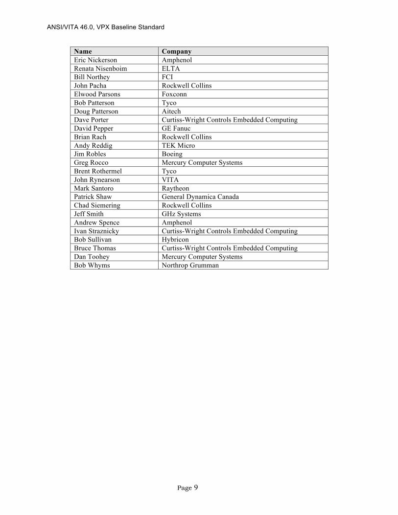
Name Company Eric Nickerson Amphenol Renata Nisenboim ELTA Bill Northey FCI John Pacha Rockwell Collins Elwood Parsons Foxconn Bob Patterson Tyco Doug Patterson Aitech Dave Porter Curtiss-Wright Controls Embedded Computing David Pepper GE Fanuc Brian Rach Rockwell Collins Andy Reddig TEK Micro Jim Robles Boeing Greg Rocco Mercury Computer Systems Brent Rothermel Tyco John Rynearson VITA Mark Santoro Raytheon Patrick Shaw General Dynamica Canada Chad Siemering Rockwell Collins Jeff Smith GHz Systems Andrew Spence Amphenol Ivan Straznicky Curtiss-Wright Controls Embedded Computing Bob Sullivan Hybricon Bruce Thomas Curtiss-Wright Controls Embedded Computing Dan Toohey Mercury Computer Systems Bob Whyms Northrop Grumman

ANSI/VITA 46.0, VPX Baseline Standard
Page 10
ANSI VITA Ballot Group The following people participated in the ANSI VITA ballot. Their participation is acknowledged and greatly appreciated.
Name Company Aaron Kaiway Spectrum Signal Processing Alan Commike Quantum3D Andre' Moorman Rockwell Collins Andrew Reddig TEK Microsystems, Incorporated Bob Patterson Tyco Electronics Bob Sullivan Hybricon Bruce Thomas Curtiss Wright Chad Siemering Rockwell Collins Chris Ciufo OpenSystems Publishing Chris Eckert GE FANUC Embedded Systems Dan P. Golden Boeing David Compston Radstone Embedded Computing Dean C. Holman Mercury Computer Systems, Inc. Douglas Patterson Aitech Elwood Parsons Foxconn Emil Kheyfets Aitech Defense Systems Ernie Domitrovits Curtiss Wright Controls Frank Hom Pentair Electronic Packaging/Schroff Gerard Drewek General Dynamics Gorky Chin Curtiss-Wright Greg Griffith Tycoelectronics Hermann Strass Technology Consulting Ivan Straznicky Curtiss Wright Controls Embedded Computing James A.. Robles The Boeing Company Jeffrey Smith GHz Systems Inc. Jerald Kilgore Rockwell Collins Jing Kwok Curtiss Wright Controls Embedded Computing John Pacha Rockwell Collins John Rynearson VITA Masayuki Mochida K.K.Rocky Michael L. Hasenfratz Northrop Grumman Michael Macpherson Curtiss-Wright Controls Embedded Computing Michael Munroe Elma Bustronic Corp Michael Thompson Pentair/Schroff Mike Macpherson Curtiss-Wright Controls Embedded Computing Nauman Arshad CWCEC Randy White Curtiss Wright Controls Inc. Richard Jaenicke Mercury Computer Systems Sean Mahrt Rockwell Collins Stewart Dewar Curtiss-Wright Controls Embedded Computing Val Gueorguiev AiTech Defense Systems Yossi David Aitech

ANSI/VITA 46.0, VPX Baseline Standard
Page 11
Acknowledgements In the development of VITA 46.0 two individuals deserve special recognition – Stewart Dewar, the VITA 46 working group chair from the inception of VITA 46 (March 2003) through May 2007, and Dean Holman, VITA 46.0 draft editor. Both individuals did superb jobs and their contributions to making VITA 46.0 an American National Standard are greatly appreciated. -- John Rynearson, VITA Technical Director Comments, Corrections and/or Additions Anyone wishing to provide comments, corrections and/or additions to this standard, please direct them to the Technical Director at the VITA office. VSO and Other Standards Should anyone want information on other standards being developed by the VSO, Product Directories, VME Handbooks, or general information on the embedded market, please contact the VITA office at the address or telephone number given on the front cover.

ANSI/VITA 46.0, VPX Baseline Standard
Page 12
1 Introduction
The embedded computing industry serves markets needing ruggedized products requiring data plane interconnect technologies which more closely follow the industry state of the art than those currently available. Switched serial technologies are available which provide significant benefits over currently deployed interconnect technologies. The benefits of switched serial interconnect technologies over parallel multi-drop buses include but are not limited to: • Higher transaction bandwidth • Higher aggregate bandwidth • Lower link latency • Less contention for the interconnect medium • Increased scalability • Less routing real estate consumed This document provides a standard mechanical format for standardization of switched serial interconnects for VMEbus applications, with specific concern taken to allow deployment in ruggedized environments. There are many candidate technologies for switched serial interconnects. These include without limitation: Ethernet through 10 GBit, Fibre Channel, InfiniBand™, Serial RapidIO™, PCI Express, Hypertransport, Infiniband and others. Each technology has its pros and cons, and the market will determine which ones will ultimately survive. The data plane defines a “playing field” on which users may implement their preferred serial interconnect.
1.1 Objectives
The objectives of this standard are: Define a 6U and 3U Eurocard format family of plug-in modules suitable for ruggedized
use. Define a suitable high-speed connector family for use in these plug-in modules. Make provision for switched serial interconnects between plug-in modules. Accommodate Open Standard technology for these switched serial interconnects. Make provision for parallel bus interconnects within the family. Make provision for additional I/O capability at the plug-in module level. Make provision for option of two level maintenance capable Line Replaceable Modules.
1.2 VITA 46 Overview
The VITA 46 family of standards comprises this base standard defining physical features of compliant components in addition to a set of protocol layer standards which define specific serial or parallel interconnects used in a system implementation. VPX is the name given to this family of standards.
ANSI/VITA 46.0, VPX Baseline Standard
Page 13
At the time of publication the following protocol standards had been defined. Please consult VITA for a current list. VITA 46.0 VPX Base Standard VITA 46.1 VMEbus Signal Mapping on VPX VITA 46.3 Serial RapidIO™ on VPX VITA 46.4 PCI Express on VPX Fabric Connector VITA 46.7 Ethernet on VPX Fabric Connector VITA 46.9 XMC/PMC/GbE Signal Mapping to 3U/6U on VPX VITA 46.10 Rear Transition Module on VPX VITA 46.11 System Management on VPX VITA 46.12 Fibre Optic Interface on VPX VITA 46.20 VPX Switch Slot Definition The VITA 46.0 base standard includes features drawn from IEEE 1101.1 and IEEE 1101.2 (for air cooled and conduction cooled plug-in modules, respectively). These features are evident in the mechanical drawings provided. The VITA 46 base standard defines physical features that enable high-speed communication in a compliant system. These features include: a 6U by 160mm by 4HP pitch Eurocard format board with high speed differential connectors, a 6U by 160mm by 4HP pitch Eurocard format board with a combination of high speed differential and single-ended connectors, and the backplane/chassis infrastructure needed to support these features. The base standard also defines similar physical features for 3U by 160mm by 4HP pitch Eurocard format, providing the same two types of connector options discussed above for 6U plug-in modules. Many features called for in the base specification will be compatible with the requirements of other standards, such as VITA-48, but this standard concerns only the IEEE 1101 compatible applications. This base standard also defines alignment and keying features used to protect the connector system. The base standard does not address the possible serial fabric configurations available in systems which utilize the standard. While the base standard does not address the use of ANSI/VITA-1.1 or VITA-41 plug-in modules, or modules which are constructed to the mechanical requirements of VITA-48, chassis and backplanes can be constructed which provide compatibility with plug-in modules built to these standards. The dot specifications allow the use of the single-ended connector allocation for parallel busses, such as VME or PCI, completing the compatibility between older standards and this one.

ANSI/VITA 46.0, VPX Baseline Standard
Page 14
1.3 Terminology
1.3.1 Specification Key Words
To avoid confusion and to make very clear what the requirements for compliance are, many of the paragraphs in this standard are labeled with keywords that indicate the type of information they contain. These keywords are listed below: Rule Recommendation Suggestion Permission Observation Any text not labeled with one of these keywords should be interpreted as descriptive in nature. These will be written in either a descriptive or a narrative style. The keywords are used as follows: Rule <chapter>-<number>: Rules form the basic framework of this standard. They are sometimes expressed in text form and sometimes in the form of figures, tables or drawings. All rules shall be followed to ensure compatibility between board and backplane designs. All rules use the “shall” or “shall not” words to emphasize the importance of the rule. The “shall” or “shall not” words are reserved exclusively for stating rules in this standard and are not used for any other purpose. Recommendation <chapter>-<number>: Wherever a recommendation appears, designers would be wise to take the advice given. Doing otherwise might result in poor performance or awkward problems. Recommendations found in this standard are based on experience and are provided to designers to speed their traversal of the learning curve. All recommendations use the “should” or “should not” words to emphasize the importance of the recommendation. The “should” or “should not” words are reserved exclusively for stating recommendations in this standard and are not used for any other purpose. Suggestion <chapter>-<number>: A suggestion contains advice, which is helpful but not vital. The reader is encouraged to consider the advice before discarding it. Some design decisions that need to be made are difficult until experience has been gained. Suggestions are included to help a designer who has not yet gained this experience. Permission <chapter>-<number>: In some cases a rule does not specifically prohibit a certain design approach, but the reader might be left wondering whether that approach might violate the spirit of the rule or whether it might lead to some subtle problem. Permissions reassure the reader that a certain approach is acceptable and will cause no problems. All permissions use the “may” words to emphasize the

ANSI/VITA 46.0, VPX Baseline Standard
Page 15
importance of the permission. The lower-case “may” words are reserved exclusively for stating permissions in this standard and are not used for any other purpose. Observation <chapter>-<number>: Observations do not offer any specific advice. They usually follow naturally from what has just been discussed. They spell out the implications of certain rules and bring attention to things that might otherwise be overlooked. They also give the rationale behind certain rules so that the reader understands why the rule must be followed.
1.3.2 VITA 46 Definitions
The following terms are used within the body of the specification. In this context, they have the following meanings. Term Definition 2-level maintenance (Two Level Maintenance)
A maintenance system where plug in modules are the field replaceable units; a subset of whose requirements are that the module provides both mechanical and ESD protection.
Air cooled a plug-in module which is intended to have heat removed by transfer to an air stream flowing over the module
Chassis Ground See Safety Ground. Conduction cooled a plug-in module which is intended to have heat removed
by transfer to the chassis through mechanical contact with a chassis component
Dedicated System A system designed for a single use or application; not available to general users. Such a system will usually embody a feature which precludes full compliance with this standard.
Differential Wafer A wafer designed for the connection of high speed (up to 5 GBaud) signaling intended for use with differential pair signals, such as LVDS.
ESD Electrostatic discharge. Ground Unless otherwise specified the term Ground means logic
ground or signal ground, not safety ground. Also referred to as RF Ground. See Safety Ground and RF Ground.
HP Horizontal Pitch of 5.08 mm or 0.2 inch (see IEEE 1101.1-1998). Thus 4HP = 0.8 inch pitch.
MultiGig RT2 7-Row A family of connectors, or their equivalent, used in VITA 46 systems for high speed interconnections.
Power Wafer A wafer providing two contacts which are intended to be used to supply prime power to a plug-in module.
RF Ground A distributed low impedance common reference between plug-in module circuitry/shields and other electrical equipment (rack, other plug-in modules, and power sources). See Safety Ground and Ground.

ANSI/VITA 46.0, VPX Baseline Standard
Page 16
Term Definition Safety Ground Plug-in module features, including ground path and
components that ensure hazardous voltages are not present on accessible hardware under single fault conditions. See Ground and RF Ground.
Single-ended (SE) wafer A single-ended wafer providing five signal contacts and two ground contacts
VME Board A plug-in module that complies with the ANSI/VITA-1.1, VME64 Extensions standard.
Vs Notation representing Prime Power from the system to the plug-in module.
VPX The name given for the family of VITA 46 specifications VXS A VMEbus Switched Serial (VITA-41) payload module
1.4 References
The following publications may be used in conjunction with this standard. Permission 1-1: The following documents, of the exact issues shown, contain provisions that through reference in this text constitute provisions of this standard to the extent specified herein. Additionally, more recent issues of applicable documents may be used provided performance, including reliability and cost, are not adversely affected. The following standards are available from the VMEbus International Trade Association. http://www.vita.com ANSI/VITA-1-2002 VME64 ANSI/VITA-1.1-1997 VME64 Extensions ANSI/VITA 38-2003 System Management for VME ANSI/VITA 47-2005 Environments, Design and Construction, Safety, and Quality for Plug-In
Units The following are available from their respective owners: IEC 512-3-1976 Electromechanical Components for Electronic Equipment; Basic Testing
Procedures and Measuring Methods IEC 60950-1:2001, Information Technology Equipment - Safety – Part 1: General Requirements. IEEE 1101.1-1998, IEEE Standards for Mechanical Core Specifications for Microcomputers
Using IEC 603-2 Connectors IEEE 1101.2-1992 IEEE Standard for Mechanical Core Specifications for Conduction-Cooled
Eurocards IEEE 1101.10-2002, IEEE Standard for Additional Mechanical Specifications for
Microcomputers Using the IEEE STD 1101.1-1991 Equipment Practice

ANSI/VITA 46.0, VPX Baseline Standard
Page 17
IEEE 1101.11-1998, IEEE Standard for Mechanical Rear Plug-in Units Specifications for Microcomputers Using IEEE 1101.1 and IEEE 1101.10 Equipment Practice
The I2C-Bus Specification, Version 2.1, January 2000 (Philips Semiconductor) IEEE 1149.1-2001 IEEE Standard Test Access Port and Boundary Scan Architecture. IPC-2221A Generic Standard on Printed Board Design

ANSI/VITA 46.0, VPX Baseline Standard
Page 18
2 VITA 46 Compliance
This section is meant as a guide to designers of VITA 46-format plug-in modules, backplanes, and systems to the major elements of the VITA 46 standard. Specific requirements for mandatory and optional elements are defined in sections 3 through 7. VITA46 compliant plug-in modules and backplanes incorporate the following major features: • Connectors which meet the requirements of this standard • Connectors in sets which meet the requirements of this standard • Keying and alignment mechanism for all slots which meet the requirements of this standard • Support for the VITA 46-defined power rails Vs1, Vs2, Vs3, 3.3V_AUX, +/-12V_AUX • Support for the VITA 46-defined utility signals: Geographical Address pins, Reference
Clock, Bussed Reserved for Future Use (RFU) differential pair, JTAG connections, System Management signals, Non-Volatile Memory Read Only (NVMRO) signal, SYSRESET*, P1 Reserved Bussed signals, and P1 Reserved for Future Use (RFU) signals. RFU signals are reserved for use by the VITA 46.0 Base Specification, not subsequent dot specifications.
• Fabric provisioning for one or more of the various protocol layer standards Recommendation 2-1: As many of the target applications for equipment defined by this standard fall within conditions covered by ANSI/VITA 47, vendors should consider offering equipment compliant with appropriate sections of the ANSI/VITA 47 standard.
ANSI/VITA 46.0, VPX Baseline Standard
Page 19
3 System
Some features required or suggested for successful implementation do not properly belong in either the plug-in module or the backplane sections. These are addressed in the following paragraphs. Throughout this document, the use of a trailing asterisk, as in GAP*, is used to indicate a logic signal which is active when at the less positive level of its allowable range. For example, in a system where GAP* is defined, it will be active when at nominal zero volts.
3.1 Safety Ground
A safety ground is intended to protect operators and users of compliant equipment from injury or exposure to possible danger due to electric shock when contacting any part of the equipment and reduce the fire hazard when combustible environments are present. The safety ground feature maintains the voltage potential at chassis ground potential during any single fault occurrence (such as the cover being bent to contact a component lead at a non-ground potential), and during many multiple fault occurrences. Rule 3-1: All plug-in modules and chassis covered by this specification shall provide a safety ground feature which has the following characteristics: • The safety ground shall not be connected to signal ground; • The plug-in module safety ground feature shall mate first and break last; • Each safety ground contact shall be capable of carrying 20 amperes; • A plug-in module’s safety ground shall not connect to any conductive component which
can be contacted by a person while the plug-in module is in use; • The resistance between the external safety ground and any cover or similar component
shall not exceed 100 milliohms in a ready to use configuration. Observation 3-1: Applications exist in which the resistance between the external safety ground and any cover, etc., must be lower than the 100 milliohms specified in Rule 3-1. Rule 3-2: The chassis vendor shall provide a separate terminal post or lug on the backplane for safety ground. The entire safety ground path, including the attachment point, shall be capable of carrying fault currents from the plug-in modules without incurring damage. Backplanes shall be documented using the following mnemonic: “SG = x” where “x” is the aggregate rated concurrent current carrying capabilities of safety ground in amps of the backplane and terminal post. Observation 3-2: The required current carrying capacity of the safety ground path depends upon many factors in the system design including the method for sensing and shutting off ground fault current flow. IPC 2221 provides guidance on determining current carrying capacity for printed circuit board materials.
ANSI/VITA 46.0, VPX Baseline Standard
Page 20
Recommendation 3-1: The terminal lug should be tied directly to earth potential unless local grounding practices dictate that the lug be bonded to chassis metalwork. Observation 3-3: The Alignment-keying device is designed to provide a safety ground path between the plug-in module and the backplane. The system design must then complete the connection to the appropriate chassis grounding point. The Alignment-keying device is designed to carry 20 Amperes of fault current. Permission 3-1: A safety ground may not be required for plug-in modules and chassis in stationary terrestrial environments which do not have any conductive components which may be contacted by a person while the system is in use. Observation 3-4: Backplanes are not required to provide a mechanism to connect Signal Ground to Safety Ground. Therefore, it is the responsibility of the system implementer to connect Signal Ground to Safety Ground in the manner required to comply with all applicable laws and regulations with respect to safety and other system requirements, including EMC.
3.2 Power Supply
3.2.1 Capacity
System designers must provide prime power to the plug-in modules via the backplane. The plug-in module power capacities are given in Section 4.8.1. Section 7.1.2 places requirements on the backplane design with regard to power delivery. Recommendation 3-2: Unless system constraints dictate otherwise, systems should allocate sufficient power supply capacity to accommodate a full card cage of compliant plug-in modules in addition to other requirements of the chassis. See section 7.1.2 for details.
3.2.2 Voltage Levels
This specification requires specific power supply voltages for compliance. All power level references in this document refer to Direct Current (DC) levels. See Section 4.8.1.1. Recommendation 3-3: System power supplies should be monotonic as they ramp to their specified final values during power up conditions. This ramp-up phase should not be less than 20 msec, neither should it exceed 150 msec. This recommendation not withstanding, systems are to be configured so that modules can operate with the specified supplies.

ANSI/VITA 46.0, VPX Baseline Standard
Page 21
3.2.2.1 3U Primary Power Input
Primary power to plug-in modules will be provided by the three power contacts labeled Vs1, Vs2 and Vs3. Rule 3-3: Vs1, Vs2 and Vs3 shall be more positive than Ground. Rule 3-4: When Vs1 is powered, the voltage on Vs1 at the backplane/plug-in module interface shall be controlled so as to maintain the voltage at +12Volts, plus or minus 5% inclusive of ripple. The nominal ripple shall not exceed 50 mVolts peak-to-peak measured over a range of 0 to 20Mhz. Rule 3-5: When Vs2 is powered, the voltage on Vs2 at the backplane/plug-in module interface shall be controlled so as to maintain the voltage between 3.25V and 3.45V inclusive of ripple. The nominal ripple shall not exceed 50 mVolts peak-to-peak measured over a range of 0 to 20Mhz. Rule 3-6: Compliant systems shall provide +5Volts on Vs3. The voltage on Vs3 at the backplane/plug-in module interface shall be controlled so as to maintain the voltage at +5Volts, plus 5%, minus 2.5% inclusive of ripple. The nominal ripple shall not exceed 50 mVolts peak-to-peak measured over a range of 0 to 20Mhz. Observation 3-5: The same connector contacts for Vs1 and Vs2 will be used for supplying different High Level Input Voltages to the plug-in modules in 6U systems. As such, 3U modules should not be installed in 6U systems.
3.2.2.2 6U Primary Power Input
Primary power to plug-in modules will be provided by one or more of the power contacts labeled Vs1, Vs2 and Vs3. Rule 3-7: When Vs1 is selected to be 48V, Vs1 shall be more positive than Vs2. Similarly, when Vs1 and Vs2 are selected to be 12V, Vs1 and Vs2 shall be more positive than Ground. Permission 3-2: When Vs1 and Vs2 are selected to be 12V, they may be connected together. Rule 3-8: When Vs1 and Vs2 are connected to 48 Volt power, the voltage on Vs1 and Vs2 at the backplane/plug-in module interface shall be controlled so as to maintain the voltage at +48Volts, plus or minus 5% inclusive of ripple. The nominal ripple shall not exceed 240 mVolts peak-to-peak measured over a range of 0 to 20Mhz. When Vs1 and Vs2 are connected to 12 Volt power, the voltage on Vs1 and Vs2 at the backplane/plug-in module interface shall be controlled so as to maintain the voltage at +12Volts, plus or minus 5%. The nominal ripple shall not exceed 50 mVolts peak-to-peak measured over a range of 0 to 20Mhz.

ANSI/VITA 46.0, VPX Baseline Standard
Page 22
Observation 3-6: The same connector contacts will be used for supplying High Level Input Voltages to the plug-in module; keying is used to protect modules from being inserted into a system with an incompatible voltage level. See Section 4.4.3. Rule 3-9: Compliant systems shall provide +5Volts on Vs3. The voltage on Vs3 at the backplane/plug-in module interface shall be controlled so as to maintain the voltage at +5Volts, plus 5%, minus 2.5% inclusive of ripple. The nominal ripple shall not exceed 50 mVolts peak-to-peak measured over a range of 0 to 20Mhz. Observation 3-7: 6U plug-in modules will need to generate +3.3V supply voltage for PMC or XMC sites.
3.2.2.3 Auxiliary Power Inputs
3.2.2.3.1 3.3V_AUX
A 3.3V auxiliary power supply is available for plug-in module use. This supply is not intended to provide primary power to the plug-in module, but rather to accommodate system management functionality which might need to operate even if the on-board power conversion circuitry fails. Rule 3-10: Compliant systems shall provide a 3.3V_AUX power supply, with capability as described in Section 7.3.7. Rule 3-11: The voltage on 3.3V_AUX at the backplane/plug-in module interface shall be controlled so as to maintain the voltage at +3.3Volts, plus or minus 5% inclusive of ripple. The nominal ripple shall not exceed 50 mVolts peak-to-peak measured over a range of 0 to 20Mhz. The plug-in module shall not draw more than 1.0 amp of 3.3V_AUX. The designer shall document the actual current requirement for 3.3V_AUX of the plug-in module. Permission 3-3: A plug-in module may connect 3.3V_AUX from the plug-in connector to 3.3V_AUX of an XMC connector.
3.2.2.3.2 12V Auxiliary Supplies
Both positive and negative 12Volts are provided as auxiliary supplies, with the intent that mezzanine modules requiring this voltage can be accommodated. The +12V_AUX and the -12V_AUX supplies are optional in systems, though it is intended that compliant backplanes will support these supplies with traces to each slot. Rule 3-12: When systems provide both 12V_AUX power supplies, they shall have the capabilities as described in Section 7.3.8.

ANSI/VITA 46.0, VPX Baseline Standard
Page 23
Rule 3-13: When implemented, the power connected to +12V_AUX at the backplane/plug-in module interface shall be controlled so as to maintain the voltage at +12Volts, plus or minus 5% inclusive of ripple. The nominal ripple shall not exceed 50 mVolts peak-to-peak measured over a range of 0 to 20Mhz. Rule 3-14: When implemented, the power connected to -12V_AUX at the backplane/plug-in module interface shall be controlled so as to maintain the voltage at -12Volts, plus or minus 5% inclusive of ripple. The nominal ripple shall not exceed 50 mVolts peak-to-peak measured over a range of 0 to 20Mhz.
3.2.3 Dielectric Separation
Observation 3-8: IPC-2221A Table 6-1, Electrical Conductor Spacing, may be used as a guide for spacing. Rule 3-15: Plug-in modules shall provide a minimum dielectric withstanding voltage of 500VDC +/-10V and a minimum resistance of 1 megaohm between safety ground and other voltage or signal conductors. Rule 3-16: Backplanes shall provide a minimum dielectric withstanding voltage of 500VDC +/-10V and a minimum resistance of 1 megaohm between safety ground and other voltage or signal conductors.
3.3 System Controller (SYS_CON)
This standard includes a definition for system controller interfaces for system management. For more information about the system controller function see Sections 7.3.2 and 4.8.3. The plug-in module or device providing the System Controller function is intended to be the source of the REF_CLK+/- signals, the SYSRESET* signal and the NVMRO signal. Depending on system requirements, it may also be the source of the System Management bus.
3.4 System-wide Connections
This section discusses connections which are required on compliant backplanes, and their intended system wide usage.
3.4.1 Reference Clock (REF_CLK+/-)
REF_CLK+/-: The Reference Clock is a bussed differential pair. It enables the entire system to synchronize to a common clock if desired. The system controller may provide this signal. If this signal is not provided by the system controller, each plug-in module must generate its own clocking signal.

ANSI/VITA 46.0, VPX Baseline Standard
Page 24
Observation 3-9: One of the uses of this signal is for all plug-in modules to synchronize to a common clock to enable the implementation of Spread Spectrum Clocking (SSC) to reduce EMI in a system. (PCIe defines the use of this mechanism for SSC). It is anticipated that a plug-in module will receive the reference clock and phase lock it up to the desired operational frequency.
3.4.1.1 Reference Clock Generator (Optional)
This standard allows protocol standards to define a Reference Clock appropriate to the needs of the individual protocol standards. The following paragraphs define this Reference Clock sufficiently that a compliant backplane can support the protocol standards’ requirements. Section 7.3.1 provides the requirements placed on compliant backplanes for the implementation of REF_CLK. Recommendation 3-4: If a fixed clock is used as the clock source, REF_CLK should have a center frequency of 25 MHz, maximum frequency deviation of +/- 100ppm, and a 50% ± 5% duty cycle. Observation 3-10: Detailed end-to-end frequency and stability requirements for reference clocks are defined in protocol standards documentation. Rule 3-17. If implemented, REF_CLK shall be driven only by the System Controller. REF_CLK shall be designed for EIA-899 M-LVDS signaling. Rule 3-18: If implemented, REF_CLK rise and fall time shall be greater than or equal to 1 ns. Series termination resistors may be required on the clock generator to meet this requirement. Permission 3-4: Plug-in modules are not required to generate or receive a reference clock. Observation 3-11: In a hybrid backplane (Section 7.5) the left most VITA 46 slot may not be physically the left most slot. A series of slots to the left of the left most VITA 46 slots might be VMEbus slots (for example).
3.4.2 JTAG Pin Allocation
This standard allows, on plug-in modules, the use of signals required to implement Test Access Port and Boundary-Scan Architecture, also known as JTAG, specified in IEEE1149.1 or IEEE1149.6. As of the writing of this standard, no suitable multi-drop JTAG Standard was codified; none is specified in this standard. Designers can implement JTAG circuitry on their plug-in modules which can then be used with standalone test fixturing (the plug-in module is completely assembled and then inserted in a fixture with access only to the backplane connector). Testing or programming, for example, could then be carried out prior to introducing the plug-in module to the final system.
ANSI/VITA 46.0, VPX Baseline Standard
Page 25
3.4.3 System Management Connections (Optional)
SM[3:0] are reserved for System Management functions, I2C, for example in a cPCI system, or IPMI. These may be defined in protocol specifications, or by the system requirements. Definition of this functionality is beyond the scope of this document; however, to assist system designers, backplane wiring requirements are provided in Section 7.3.5. Permission 3-5: Implementation of specific System Management connections is not required. See also Section 4.8.8 for requirements on plug-in modules.
3.4.4 Non-Volatile Memory Read Only (Optional)
A system wide signal which, when asserted, prevents any non-volatile memory from being updated. This allows systems with security sensitivity the ability to run classified or sensitive data without the concern that the data will be kept once power has been removed. This standard does not impose requirements on the source or the timing of this signal. It is expected that it will be driven by the plug-in module or device designated as System Controller. Recommendation 3-5: This signal should be derived from a physical device, a jumper for example, whose state can be observed by an operator.
3.4.5 SYSRESET*
This open-collector signal is provided to system designers as a method of ensuring that a “clean” start up can occur. Requirements placed on plug-in modules (primarily dealing with power-up and –down scenarios) are described in Section 4.8.11; those for compliant backplanes in Section 7.3.9. Observation 3-12: The threshold limits defined in Section 4.8.11 are intended to minimize hardware resets to the plug-in modules during power rail noise transients while ensuring stable potential and current supplies to the plug-in modules. These definitions are predicated on the assumption that the plug-in units will use dc/dc converters on the Vs1, Vs2 rails, while utilizing the Vs3, 3.3V_AUX, and 12V_AUX (+-) rails directly for internal circuits.
3.5 Status Indicators
Permission 3-6: Whether on a chassis or on plug-in modules installed in a system, status indicators may be used to assist an operator or other user. Recommendation 3-6: Status indicators should be compliant with ANSI/VITA 40, Status Indicator Standard.
ANSI/VITA 46.0, VPX Baseline Standard
Page 26
3.6 Slot Type Indication
Some indication is desirable to indicate to an operator or other user the type of connectors installed in the backplane at a particular slot. As these connectors are under the control of the protocol specifications, this is particularly important. Recommendation 3-7: Keying should be used to identify slot types with sufficient differentiation to allow plug-in modules to be inserted without fear of damage, either to the plug-in module or to the system. See Section 4.4.3.
ANSI/VITA 46.0, VPX Baseline Standard
Page 27
4 Common Requirements
4.1 Overview
Some of the requirements of this base specification apply to both 3U and 6U plug-in modules. These are covered in this section. In addition, Section 1.1 describes requirements and recommendations dealing with signal integrity which apply to both plug-in modules and backplanes. Plug-in module dimensions are shown in the assembly drawings in Figures A-1 and A-2 for a 3U plug-in module, and in Figures A-3 and A-4, for a 6U plug-in module. In addition, Appendix B includes fabrication drawings for backplanes and Appendix C includes PCB fabrication drawings for both air-cooled and conduction-cooled 3U and 6U modules. Options for covers which provide ESD and handling protection are also included in this section.
4.2 Connectors
Rule 4-1: VITA 46 plug-in modules shall utilize a single 8-wafer PCB 7-Row connector section in addition to between two and six 16-wafer PCB 7-Row (or equivalent) connector sections. See Table 4-1 for component information. The number of 16-wafer sections depends on the size of the module and the possible incorporation of alternate user defined connector implementations. Table 4-1 Module P0 and P1 Connectors
Connector Description P0 Left end module, 8 wafers, right angle 1 P1 Center module, 16 differential wafers, right angle2
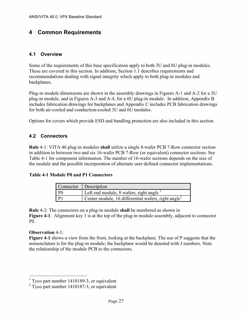
Rule 4-2: The connectors on a plug-in module shall be numbered as shown in Figure 4-1. Alignment key 1 is at the top of the plug-in module assembly, adjacent to connector P0. Observation 4-1: Figure 4-1 shows a view from the front, looking at the backplane. The use of P suggests that the nomenclature is for the plug-in module; the backplane would be denoted with J numbers. Note the relationship of the module PCB to the connectors.
1 Tyco part number 1410189-3, or equivalent 2 Tyco part number 1410187-3, or equivalent
ANSI/VITA 46.0, VPX Baseline Standard
Page 28
3U 6U
Figure 4-1 Connector Identification for 3U and 6U Modules
Alignment Key 3
Alignment Key 2
Alignment Key 1
Module PCB

ANSI/VITA 46.0, VPX Baseline Standard
Page 29
Rule 4-3: P0 shall utilize an 8-wafer connector section. Rule 4-4: The 8-wafer section in P0 shall be loaded with three Power wafers, in positions one, two and three. See Section 4.8.1. Rule 4-5: The 8-wafer section in P0 shall be loaded with three of the single-ended 5-signal/2-ground style wafers, in positions four, five and six. The single-ended contacts are to be used for routine low speed or non-differential ‘housekeeping’ functions, like geographical addressing and system management functions. Rule 4-6: In P0, differential wafers shall be used in positions seven and eight. Rule 4-7: In P0, unused differential connections provided shall be Reserved for Future Use.
4.3 Form Factor and Outline
This base specification uses IEEE 1101.1 and 1101.2 outlines for compliant plug-in modules. Other form factors are amenable to use with the connectors specified in Section 4.2, but are not codified here. Rule 4-8: Air cooled plug-in modules which are 3U in height shall meet the dimensions of Figure A-1. Rule 4-9: Conduction cooled plug-in modules which are 3U in height shall meet the dimensions in Figure A-2 and Figure A-8. Rule 4-10: Air cooled plug-in modules which are 6 U in height shall meet the dimensions in Figure A-3. Rule 4-11: Conduction cooled modules which are 6U in height shall meet the dimensions in Figure A-4 and Figure A-8.
4.4 Alignment and Keying
4.4.1 Background and Assumptions
The VITA 46 keying method consists of a flat face on the backplane-side alignment and keying pin that must line up with a matching flat face on the inside of a hole in the alignment-keying device on the plug-in module. See Figure 4-2 for a pictorial representation of the VITA 46 keying system.

ANSI/VITA 46.0, VPX Baseline Standard
Page 30
Alignment & Keying P in
A lignment & Keying Socket
90° 45° 0° 315° 270° Figure 4-2 VITA 46 Keying System
4.4.1.1 Philosophy
The VITA 46 keying method provides 125 unique key settings on a 6U card and 25 unique key settings on a 3U card. As there are not enough keying options to define settings for backplane fabric type, parallel bus type, and daughter card connector types, and to leave the user with a reasonable range of key settings to differentiate between modules within a given system, this standard defines only keying which is essential. It is deemed essential that keying be defined to prevent a plug-in module from being inserted into a slot that has an incompatible High Voltage (Vs1/Vs2) Input (a 12V card plugged into 48V backplane or vice versa).
4.4.1.2 Backplane Key
The angular position of the flat face on the backplane keying pin is controlled by inserting the keying pin into the backplane at different angular positions. This position is controlled by the location of a tangential hole drilled into the backplane PCB beside the main hole for the keying pin, into which a rib on the base of the keying pin fits. The backplane keying pin has five allowed angular positions, referred to by angle (one of 0, 45, 90, 270, or 315 degrees). It is possible to fabricate a backplane with multiple holes for the rib of the backplane alignment pin as long as the holes are not in adjacent angular positions. The backplane could therefore have holes for positions 0, 90, and 270, or for positions 45 and 315.
4.4.1.3 Plug-in Module Key
There are six different alignment-keying devices for the plug-in modules, five that match each of the allowed angles of the backplane keying pin, plus one type with no flat on the inside of the hole, allowing the plug-in module keying device to be mated with the backplane pin no matter the angle of the latter, this is the "unkeyed” plug-in module keying device. See Table 4-2 for representative part numbers for the alignment and keying modules for plug-in modules.
ANSI/VITA 46.0, VPX Baseline Standard
Page 31
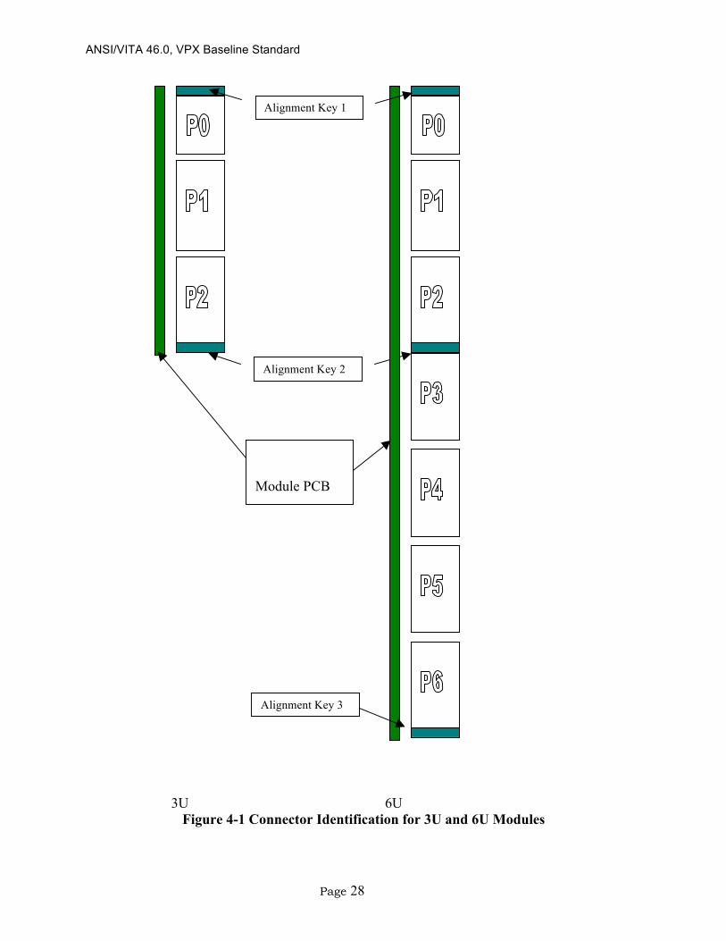
Table 4-2 Alignment and Keying Module Part Numbers for Plug-in Modules
Plug-in Module Alignment and Keying Module Angle Setting 0° 3 45° 4 90° 5 270° 6 315° 7 - (unkeyed, mates with any backplane keying pin) 8
4.4.2 Definitions
Rule 4-12: For the purposes of specifying the VITA 46 keying provisions, the positions of the backplane alignment and keying pins and the daughter card alignment-keying devices shall be identified as follows:
- the position adjacent to the P0 connector on both 6U and 3U modules is referred to as position 1
- the position adjacent to the P2 connector on both 6U and 3U modules is referred to as position 2
- the position adjacent to the P6 connector position on 6U modules is referred to as position 3
4.4.3 Keying Rules
Rule 4-13: Alignment-keying devices shall be used. Permission 4-1: These devices may provide keying as defined by the system designer. Rule 4-14: A 3U plug-in module shall utilize two alignment-keying devices; a 6U plug-in module shall utilize three. Rule 4-15: These shall be located as shown in Figure 4-1, Figure C-1 and Figure C-2. Rule 4-16: The alignment-keying sockets in positions 1 and 3 on a 6U conduction cooled plug-in module, and positions 1 and 2 on a 3U plug-in module, are contained within the card guide slot of a IEEE 1101.2 compliant chassis. As a result, the screw used for attachment of the alignment- 3 Tyco part number 1-1469492-1, or equivalent 4 Tyco part number 1-1469492-2, or equivalent 5 Tyco part number 1-1469492-3, or equivalent 6 Tyco part number 1-1469492-7, or equivalent 7 Tyco part number 1-1469492-8, or equivalent 8 Tyco part number 1-1469492-9, or equivalent

ANSI/VITA 46.0, VPX Baseline Standard
Page 32
keying socket to the PCB shall have a head height that does not interfere with conduction plug-in module insertion or extraction, i.e. meets the 0.510" relaxed max. card edge dimension in IEEE 1101.2. To achieve this, a low profile head height screw9 may be used, or a flat head screw with its associated countersink may be required for thicker PCBs. Recommendation 4-1: On 6U plug-in modules, the alignment-keying device in position #1 should be keyed in accordance with the High Voltage Power Input that the plug-in module uses. This keying module should be referred to as the voltage keying module. Observation 4-2: For 3U plug-in modules keying for input voltage is not required as all prime power inputs have permanently dedicated power wafers, in contrast to the 6U case where either 12V or 48V may be input on the Vs1 and Vs2 power wafers. Rule 4-17: For the 6U case, plug-in module keying modules in positions #2 and #3 shall be designated for slot-specific keying. For the 3U case, plug-in module keying modules in positions #1 and #2 shall be designated for slot-specific keying. Recommendation 4-2: For the 6U case, if the High Voltage Power Input used by the plug-in module is 48V, the plug-in module voltage keying device that is installed should be one of two types - either 45 or 90 Recommendation 4-3: For the 6U case, the preferred angle for the plug-in module voltage keying module for the 48V case is 45 and this should be used unless specific system requirements for a user keying range greater than 25 (6U modules) exist. All standard catalog 48V plug-in modules should use this setting. Recommendation 4-4: For the 6U case, if the high voltage power input used by the plug-in module is 12V, the plug-in module should have either the 315 degree or 0 degree alignment-key installed. Recommendation 4-5: For the 6U case, the preferred angle for the plug-in module voltage keying device for the 12V case is 315 and this should be used unless specific system requirements for a user keying range greater than 25 exist. All standard catalog 12V plug-in modules should use this setting. Recommendation 4-6: For the 6U case, if the plug-in module does not use any high voltage power input (Vs1 and Vs2 are no-connects), the plug-in module keying device that is installed should be of the unkeyed type that will mate with a backplane keying pin positioned at any angle. Recommendation 4-7: For the 6U case, the plug-in module voltage keying device of type 270 should be Reserved for Future Use.
9 Tyco part number 1410946-1 or equivalent.

ANSI/VITA 46.0, VPX Baseline Standard
Page 33
Recommendation 4-8: To facilitate ease of system integration, standard catalog 6U plug-in modules should be delivered with keying devices #2 and #3 installed that are of the unkeyed type, and standard catalog 3U plug-in modules should be delivered with keying devices #1 and #2 installed that are of the unkeyed type. Observation 4-3: Users who wish to apply slot-specific keying can either replace the standard vendor-supplied non-keyed keying device(s) on the plug-in modules or make special arrangement with the vendor to install the keying device(s) of their choice. Observation 4-4: The Alignment-keying device is designed to provide a safety ground path between the plug-in module and the appropriate chassis grounding point.
4.5 Two Level Maintenance (Optional)
Achieving 2-level maintenance requires both the ability to isolate system faults and to safely remove and replace the faulty module(s) in the field. The latter implies the need for both mechanical and ESD protection for plug-in modules. This specification makes recommendations for meeting those requirements for the connectors. Full mechanical and ESD protection, including covers for plug-in modules, is addressed in VITA 48. See also VITA 47, Section 4.11 for levels of electrostatic discharge resistance. Observation 4-5: The standard connectors specified for use with this standard are ESD-protected. Recommendation 4-9: Plug-in modules should use ESD-protected connectors for all optional connectors. Recommendation 4-10: Plug-in modules should provide a RED 630 nm nominal(Range: 615-650 nm) status indicator, that when active (steady on), indicates that a plug-in module fault has been detected. The status indicator should remain active after prime power is removed and until the plug-in module is removed, as long as 3.3V_AUX power is applied. Visibility should conform to ANSI/VITA 40, Recommendation 2.9-4: Visibility at side viewing angles and distances, Recommendation 2.9-5: Visibility under different lighting conditions, and Recommendation 2.9-7: False illumination of indicators due to ambient light.
4.6 Connector Pin Definition - P0
Rule 4-18: Pins in connector P0 shall be defined as shown in Table 4-3. This pinout is defined using three (3) power, three (3) single-ended wafers and two (2) differential wafers.

ANSI/VITA 46.0, VPX Baseline Standard
Page 34
Table 4-3 P0 Utility Connector
Wafer Type Row G Row F Row E Row D Row C Row B Row A 1 Power Vs1 Vs1 Vs1 No Pad Vs2 Vs2 Vs2 2 Power Vs1 Vs1 Vs1 No Pad Vs2 Vs2 Vs2 3 Power Vs3 Vs3 Vs3 No Pad Vs3 Vs3 Vs3 4 Single-ended SM2 SM3 GND -12V_AUX GND SYSRESET* NVMRO 5 Single-ended GAP* GA4* GND 3.3V_AUX GND SM0 SM1 6 Single-ended GA3* GA2* GND +12V_AUX GND GA1* GA0* 7 Differential TCK GND TDO TDI GND TMS TRST* 8 Differential GND REF_CLK- REF_CLK+ GND RES_BUS- RES_BUS+ GND Signal definitions for the P0 connector are given in Table 4-4, with additional information provided in the text following. Table 4-4 P0 Signal Definitions Pin/Signal Description Vs1 High Voltage Power Input 1 (see text) Vs2 High Voltage Power Input 2 (see text) Vs3 Low Voltage Power Input (see text) GA[4:0]*, GAP* Geographical Address Inputs 0-4, Parity SM[3:0] System Management connections RES_BUS+/- Bussed: Reserved for Future Use 3.3V_AUX 3.3V Auxiliary power, System Management +/- 12V_AUX Auxiliary Power Supplies SYSRESET* System Reset REF_CLK+/- Reference Clock 25 MHz (see text) NVMRO Non-Volatile Memory Read Only TCK, TMS, TRST*, TDI, TDO (wafer 7) JTAG Signals (see text) No Pad The construction of the connector wafer is such that
there is no circuit pad in this location
4.7 Electrical Budgets for Protocol Standards
The electrical parameters for a high speed serial Link are subdivided into three separate Components.
- VITA 46.x Board Tx interconnect (including mated connectors and connector via footprints on the backplane)
- VITA 46.x Backplane (no connector) - VITA 46.x Board Rx interconnect (including mated connectors and connector via
footprints on the backplane) Observation 4-6: The intent of this definition is to ease measurement of the parameters in the following rules. Plug-in module measurement will be performed by installing the plug-in module under test into a calibrated backplane and backplane measurement will be performed by installing a calibrated plug-in module into the backplane under test.
ANSI/VITA 46.0, VPX Baseline Standard
Page 35
Rule 4-19: Each layered protocol standard shall specify the budget for each of the following parameters for the VITA 46.x Board Tx interconnect Component of the link as outlined above. • AC Coupling requirements (where required) • Insertion Loss (Voltage Transfer Function) • Impedance (or Return Loss) • Jitter • Lane-to-Lane skew • Crosstalk (near end and far end) • Transmitter de-emphasis • Skew within a differential pair Rule 4-20: Each layered protocol standard shall specify the budget for each of the following parameters for the VITA 46.x Backplane Component of the link as outlined above. • Insertion Loss (Voltage Transfer Function) • Impedance (or Return Loss) • Lane-to-Lane skew • Crosstalk (near end and far end) • Skew within a differential pair Observation 4-7: The intent is that any skew within a differential pair introduced by the connector system be taken into account by the plug-in module. The skew within a differential pair in the backplane will be compensated entirely within the backplane routing Rule 4-21: Each layered protocol standard shall specify the budget for each of the following parameters for the VITA 46.x Board Rx interconnect Component of the link as outlined above. • AC Coupling requirements (where required) • Insertion Loss (Voltage Transfer Function) • Impedance (or Return Loss) • Jitter • Lane-to-Lane skew • Crosstalk (near end and far end) • Skew within a differential pair Observation 4-8: Typical values for an FR406 Board Tx or Rx interconnect with 3” trace lengths are as follows: • Insertion Loss (Voltage Transfer Function): @1.25Ghz ~ 0.8dB, @1.56 Ghz ~ 1.0dB • Impedance: 100 Ohms +/- 10% (Return Loss is protocol specific) • Lane-to-Lane skew: 100 ps • Crosstalk (near end and far end): < 1% with 100 ps rise time • Skew within a differential pair: 3 ps Observation 4-9: Typical values for an FR406 backplane with 16” trace lengths are as follows: • Insertion Loss (Voltage Transfer Function): @1.25Ghz ~ 4.6dB, @1.56 Ghz ~ 5.75dB • Impedance (or Return Loss): 100 Ohms +/- 10% • Lane-to-Lane skew: 100 ps

ANSI/VITA 46.0, VPX Baseline Standard
Page 36
• Crosstalk (near end and far end): < 6% with 100 ps rise time • Skew within a differential pair (incl. connectors): 10 ps
4.8 Signal Definition – P0
The use of a trailing asterisk, as in GAP*, is used to indicate a logic signal which is active when at the less positive level of its allowable range. For example, in a system where GAP* is defined, it will be active when at nominal zero volts.
4.8.1 Power
This specification provides for three Power Supply voltages. It is the intent of the specification that these be maintained as separate delivery paths. It is also the intent of this specification that primary power to the plug-in module be provided by some combination of Vs1, Vs2 and/or Vs3. Permission 4-2: Plug-in modules may use the appropriate combination of Vs1, Vs2 and Vs3 to accommodate the design requirements. However, to claim conformance to this standard, plug-in modules must be capable of being inserted in a standard keyed location. See Section 4.4.3.. Recommendation 4-11: Plug-in modules should include an internal power supply control system that holds the module in reset until input voltages are stable for a suitable interval. For many system applications, this time will be 200-500 milliseconds. Observation 4-10: Depending on module design and intended application, more complex power control routines may be appropriate. Rule 4-22: Plug-in modules shall be designed to accommodate any combination of power supply power up and power down sequences without causing board failure. Recommendation 4-12: The End of Life maximum current ratings shown in Table 4-5 should be used.

ANSI/VITA 46.0, VPX Baseline Standard
Page 37
Table 4-5 Power Wafer Current Ratings Power Wafer Current Rating for 30ºC Temp. Rise (at Wafer Pad and Backplane Connector Contact Interfaces) Power plane thickness in plug-in module and backplane
2 ounce copper 1 ounce copper
Number of Wafers across which power is dissipated
3 wafers 2 wafers 1 wafer 3 wafers 2 wafers 1 wafer
Current Allowed per pad (A)
6 8 11.5 5 7 11
Current Allowed per wafer (A)
12 16 23 10 14 22
Total Current Allowed per connector (A)
36 32 23 30 28 22
These current ratings are dependent on several variables, such as: • Heatsinking, e.g. copper plane thickness and size, connected to power pins. The above ratings are from test data for 1 and 2 ounce copper planes within test plug-in modules and backplane. • Thermal management, e.g. cooling method for a plug-in module. The above ratings are from test data where cooling was to still ambient air. • Contact resistance degradation from environmental exposure. The above ratings assume approximately 20% increase in contact resistance from initial to end-of-life values. Larger increases would result in proportionately lower current ratings Rule 4-23: Keying shall be used to differentiate plug-in modules by input power acceptability. See Section 4.4. Observation 4-11: The power arrangement specified is intended to support both 3U and 6U designs. As input power levels of up to 276 Watts for 3U and 768 Watts for 6U are allowed, it is possible to bring more power into a 3U plug-in module, or even a 6U plug-in module, than can be dissipated. Protection of the power input may be appropriate.
4.8.1.1 High Voltage Power Inputs
Two high voltages are allowed in this standard. Contacts are allocated in power wafers to supply higher voltage power to the plug-in module. This standard calls for Vs1 and Vs2 named contacts in P0.

ANSI/VITA 46.0, VPX Baseline Standard
Page 38
Rule 4-24: 6U compliant systems shall use voltage levels of either 48V or 12V, but not both. If neither 48V nor 12V supplies are needed, then Vs1 and Vs2 shall not be supplied with any power. Rule 4-25: Power delivery contact shall be more positive that the Return for that voltage.
4.8.1.1.1 6U High Voltage Power Input
Rule 4-26: The High Voltage Power Input shall be 48V, 12V, or not driven.
4.8.1.1.2 6U Use of 48V for High Voltage Power Input
Rule 4-27: When the High Voltage Power Input is 48V, Vs1 shall be 48V and Vs2 shall be 48V Return. See Section 3.2.2.2 for more details on this power supply. Permission 4-3: The 48V power supply may be isolated.
4.8.1.1.3 6U Use of 12V for High Voltage Power Input
Rule 4-28: When the High Voltage Power Input is 12V, both Vs1 and Vs2 shall be 12V. See Section 3.2.2.2 for more details on this power supply. This power supply shall not be isolated. Permission 4-4: When Vs1 and Vs2 are selected to 12V, they may be connected together.
4.8.1.1.4 3U High Voltage Power Input
Rule 4-29: For 3U designs, the High Voltage Power Input Vs1 shall be 12V and Vs2 shall be 3.3V. See Section 3.2.2.1 for more details on this power supply. These power supplies shall not be isolated.
4.8.1.2 Vs3
Vs3 is allocated in power wafers to supply a lower voltage power to the plug-in module. Rule 4-30: The Vs3 power supply shall be +5V, See Section 3.2.2.2 for more details on this power supply. This power supply shall not be isolated.
4.8.2 Geographical Addressing
GA[4:0]* plus GAP*: Pins allocated for system-wide geographical addressing.
ANSI/VITA 46.0, VPX Baseline Standard
Page 39
Rule 4-31: GA0* shall be the LSB (least significant bit) of the address. See Section 7.2 for information on the backplane assignments for these signals. Rule 4-32: Plug-in modules shall be designed for 3.3V signaling on these pins. The plug-in module shall limit the current through each geographical address pin to a maximum of 2 mA. The voltages for logic high and logic low shall be as defined in section 4.8.12.3.
4.8.3 System Controller (SYS_CON)
A module is designated a as the System Controller (SYS_CON) when the SYS_CON mode is set. This mode is set by when the SYS_CON* pin is connected to ground on the backplane. Rule 4-33: The SYS_CON* line shall indicate if the module should or should not be the System Controller.
SYS_CON* = grounded; indicates that this module is the System Controller SYS_CON* = open; indicates that this module is not the System Controller.
Rule 4-34: The plug-in module shall limit the current through the SYS_CON* pin to a maximum of 2 mA. The voltages for logic high and logic low shall be as defined in section 4.8.12.3. Observation 4-12: A 5% 10Kohm pull up resistor on the plug-in module will easily meet the 2 mA rule. Observation 4-13: There is no explicit System Controller redundancy capability. If the module or device designated as the System Controller fails, there is no mechanism defined to determine which other module or device will assume the System Controller function. Rule 4-35: All VITA 46 plug-in modules with the capability to be the VITA 46 System Controller shall monitor the SYS_CON* pin to determine if the module will be the System Controller.
4.8.4 Reference Clock (Optional)
REF_CLK+/-: The Reference Clock is a bussed differential pair. It enables the entire system to synchronize to a common clock if desired. This signal may be driven by the System Controller. All plug-in modules may receive this signal. If this signal is not generated, each plug-in module must generate its own clocking signal. See Section 3.4.1 and Section 7.3.1 for additional details from both the system and backplane points of view. Rule 4-36: The Plug-in module shall be designed with the following characteristics:
a) Support for 3.3V EIA-899 M-LVDS signaling on these pins. b) The differential impedance of the stubs on the plug-in module shall be 100 Ohms ± 10%. c) No termination shall be provided on the plug-in module.

ANSI/VITA 46.0, VPX Baseline Standard
Page 40
d) The stub length on the plug-in module, not including the RT2 connector, shall be less than 1.0 inch (25.4 mm).
e) Near end crosstalk shall be limited to less than 5 %.
Permission 4-5: On receive only plug-in modules, series resistors of greater than 250 Ohms may be used within 1.0 inch (25.4 mm) of the connector to allow for longer stub lengths of up to 2.56 inches (65 mm), provided that the effect of a slower rise-time is acceptable. The RC time constant approaches 4 ns for the 2.56 inch (65 mm) length with 250 Ohm resistors.
4.8.4.1 Reference Clock Generator (Optional)
Section 3.4.1.1 provides guidance for the Reference Clock Generator, including center frequency, duty cycle and rise and fall times. Permission 4-6: A plug-in module is not required to generate a reference clock.
4.8.4.2 Reference Clock Receiver (Optional)
Rule 4-37: All Plug-in modules that use reference clock shall provide a means of detecting the presence of the reference clock and have the ability to select the backplane clock or an internal clock. Permission 4-7: A plug-in module is not required to use or receive reference clock.
4.8.5 Non-Volatile Memory Read Only (Optional)
NVMRO: (Non-Volatile Memory Read Only) A system wide signal which, when asserted, prevents any non-volatile memory from being updated. This allows systems with security sensitivity the ability to run classified or sensitive data without the concern that the data will be kept over power cycles. This also supports the updating or protection of program store memory. See Section 7.3.6 for compliant backplane requirements. Recommendation 4-13: NVMRO should be driven by the plug-in module or device designated as System Controller. See Section 4.8.3 This standard does not impose requirements on the source or the timing of this signal. Recommendation 4-14: Plug-in modules which observe this signal should be designed to accept transitions on this signal at any time while valid power is applied. Observation 4-14: Many implementations of this capability observe this signal only at power up; transitions on this signal at other times are ignored in these implementations. System designers contemplating the use of this capability are advised to determine plug-in module and controller capabilities prior to specification.
ANSI/VITA 46.0, VPX Baseline Standard
Page 41
Rule 4-38: NVMRO shall be an active high open collector signal. Rule 4-39: The NVMRO line shall conform to the electrical characteristics as defined in section 4.8.12.1. Rule 4-40: When asserted, plug-in modules which observe this signal shall disable the writing of all non-volatile memory. Observation 4-15: The use of an active high NVMRO control signal with a pull-up resistor on the backplane has the effect that the default condition is that Non-Volatile Memory in a system is protected from being written. A user must intentionally pull the bussed NVMRO signal low, possibly via a test connector or jumper, in order to enable writing to the NVMRO in a system. In effect, this acts as a write enable when grounded. See backplane section 7.3.6 for the NVMRO pull-up resistor value.
4.8.6 Reserved for Future Use Differential Pair
RES_BUS+/-: This pair is bussed, and Reserved for Future Use by the VITA 46.0 Base Specification. Section 7.3.3 describes the transmission line terminations on the backplane for these signals. Recommendation 4-15: Plug-in modules should not route to the RES_BUS pins.
4.8.7 JTAG Pin Allocation (Optional)
This standard allows, on plug-in modules, the use of signals required to implement Test Access Port and Boundary-Scan Architecture, also known as JTAG, specified in IEEE1149.1. The complete specification of these signals is beyond the scope of this document; for additional information on JTAG signaling and usage, please see the appropriate specification. Five pins in P0 are allocated for JTAG. At the writing of this standard, no suitable multi-drop JTAG Standard was codified; therefore, none is specified in this standard. However, compliant backplane requirements are defined in Section 7.3.4. Observation 4-16: This allows plug-in modules to have a standard pin-out, allowing standardized JTAG chain access during the manufacturing process. Permission 4-8: JTAG support is optional on compliant plug-in modules. Rule 4-41: The JTAG lines shall conform to the electrical characteristics as defined in section 4.8.12.3.

ANSI/VITA 46.0, VPX Baseline Standard
Page 42
4.8.8 System Management Connections (Optional)
SM[3:0] are reserved for System Management functions, I2C, for example in a cPCI system, or IPMI. These may be defined in protocol specifications, or by the system requirements. Definition of this functionality is beyond the scope of this document; however, to assist system designers, Section 7.3.5 provides requirements for compliant backplanes. When utilized as single-ended signals, this section defines SM0 and SM2 as clock lines, and SM1 and SM3 as data lines. When only a single I2C bus is implemented, SM0 and SM1 should be used. If differential pairs are implemented, then SM0 and SM1 should form one pair, while SM2 and SM3 should constitute the second pair. Rule 4-42: Plug-in modules shall be designed for 3.3V signaling on this pin. The plug-in module shall limit the current through this pin to a maximum of 2 mA.
4.8.9 3.3V_AUX
The 3.3V_AUX provides an auxiliary power supply for plug-in module use. This supply is not intended to provide primary power to the plug-in module, but rather to accommodate system management functionality which may need to operate even if the on-board power conversion circuitry fails. See Section 3.2.2.3.1 for more details on this supply. Rule 4-43: The plug-in module shall limit the current draw on this supply to a maximum of 1.0 A.
4.8.10 12V_AUX (+ and -) (Optional)
Positive and negative 12Volts is provided, with the intent that mezzanine modules requiring this voltage can be accommodated. See Section 3.2.2.3.2 for more details on these power supplies. Rule 4-44: The plug-in module shall limit the current draw on either of these supplies to a maximum of 1.0 A.
4.8.11 SYSRESET*
This signal is provided to system designers as a method of ensuring that a “clean” start up can occur. Section 7.3.9 requires that this signal be connected to all slots of a compliant backplane. Backplane termination requirements for SYSRESET* are in section 7.3.9. Rule 4-45: SYSRESET* shall be an active low open collector signal. Rule 4-46: The SYSRESET* line shall conform to the electrical characteristics of section 4.8.12.2.
ANSI/VITA 46.0, VPX Baseline Standard
Page 43
Rule 4-47: When this signal is asserted low, a plug-in module which observes SYSRESET* shall initialize itself to a known state. Rule 4-48: The System Controller shall drive this signal for a minimum of 10 milliseconds, measured from the time that power has stabilized. When driven by a plug-in module other than the System Controller, the SYSRSET* signal shall have a minimum active low pulse width of 10ms. Recommendation 4-16: When SYSRESET* is deasserted it is possible that one or more plug-in modules may not yet be fully initialized and ready to provide full functionality. The system designer should be aware of this possibility and should ensure correct system start-up by the selection of compatible modules and/or the provision of an appropriate synchronizing mechanism. Recommendation 4-17: The System Controller should include a power supply monitor which should require the assertion of SYSRESET* under the following conditions:
• During power-up: while any of the backplane power rails are below the following levels: o 45.6V when Vs1, Vs2 (Section 3.2.2.2) provide 48V (6U case) o 11.4V when Vs1, Vs2 (Section 3.2.2.2) provide 12V (6U case) o 11.4V on Vs1 (Section 3.2.2.2) (3U case) o 3.25V on Vs2 (Section 3.2.2.2) (3U case) o 4.75V on Vs3 (Section 3.2.2.2) o 3.13V on 3.3V_AUX (Section 3.2.2.3.1) o 11.4V Magnitude on either 12V_AUX(+-) (Section 3.2.2.3.2)
• During power down: once any of the backplane power rails drop below the following levels for more than 50ms:
o 43.8V when Vs1, Vs2 provide 48V (6U case) o 10.8V when Vs1, Vs2 provide +12V (6U Case) o 10.8V on Vs1 (3U case) o 3.0V on Vs2 (3U case) o 4.5V on VS3 o 3.0V on 3.3V_AUX o 10.8V Magnitude on either 12V_AUX (+-)
Permission 4-9: The power supply monitor function may be a part of another system component (the power supply, for example). Recommendation 4-18: As non-monotonicity could produce false starts in power sequencing, the power monitor system should allow for that possibility, resetting the sequence if necessary. However, the design should also preclude the possibility of operating in an endless loop of reset-try to come up-reset. Permission 4-10: SYSRESET* may be asserted to accommodate other system functions or requirements.

ANSI/VITA 46.0, VPX Baseline Standard
Page 44
Permission 4-11: A plug-in module other than the System Controller may also drive SYSRESET*. Rule 4-49: The SYSRESET* signal received by the plug-in module shall be debounced prior to application to internal circuitry. Observation 4-17: In the case of a hybrid backplane, each section obeys its own rules for the assertion of SYSRESET*. In this case the VITA 46 section may remain in reset for a longer period after power up than it otherwise would, since the minimum required reset duration for VME is longer than the minimum required reset duration for VITA 46.
4.8.12 Electrical standards
4.8.12.1 Low Current Open Collector Electrical Characteristics
Rule 4-50: A VPX signal defined to meet low current open collector electrical characteristics (OC-low) shall meet the following characteristics:
a. be an active low open collector signal b. Steady-state driver low output level < 0.6 V
a. Low state sink current: IOL > 24 mA b. Low state voltage: VOL < 0.6V at IOL = 24 mA
c. Steady-state receiver low input level < 0.8 V d. Steady-state receiver high input level > 2.0 V e. be designed for 3.3V signaling on this pin f. limit the capacitive load on this signal to 20 picoFarads maximum g. As a receiver, the plug-in module shall limit the current through this pin to a maximum
of 100uA. h. Current sourced by board at 0.6 V, including leakage current: IOZL+IIL < 600 uA i. Current sunk by board at 2.4 V, including leakage current: IOZH+IIH < 50 uA j. Total capacitive load on signal, including signal trace: CT < 20 pF
4.8.12.2 High Current Open Collector Electrical Characteristics
Rule 4-51: A VPX signal defined to meet high current open collector electrical characteristics (OC-High) shall meet the following characteristics
a. be an active low open collector signal b. Steady-state driver low output level < 0.6 V
a. Low state sink current: IOL > 48 mA b. Low state voltage: VOL < 0.6V at IOL = 48 mA
c. Steady-state receiver low input level < 0.8 V d. Steady-state receiver high input level > 2.0 V e. be designed for 3.3V signaling on this pin f. limit the capacitive load on this signal to 20 picoFarads maximum

ANSI/VITA 46.0, VPX Baseline Standard
Page 45
g. As a receiver, the plug-in module shall limit the current through this pin to a maximum of 100uA.
h. Current sourced by board at 0.6 V, including leakage current: IOZL+IIL < 600 uA i. Current sunk by board at 2.4 V, including leakage current: IOZH+IIH < 50 uA j. Total capacitive load on signal, including signal trace: CT < 20 pF
Observation 4-18: The OC-high electrical characteristic is defined to be compatible to ANSI VITA 1 levels.
4.8.12.3 Totem Pole Electrical Characteristics
Rule 4-52: A VPX signal defined to meet totem pole electrical characteristics (TP) shall meet the following characteristics
a. Steady-state driver low output level < 0.6 V a. Low state sink current: IOL > 8 mA b. Low state voltage: VOL < 0.6V at IOL = 8 mA
b. Steady-state receiver low input level < 0.8 V a. Current sourced by board at 0.6 V, including leakage current: IOZL+IIL < 600 uA
c. Steady-state driver high output level > 2.4 V a. High state source current: IOH > 400 uA b. High state voltage: VOH > 2.7V at IOH = 400 uA
d. Steady-state receiver high input level > 2.0 V a. Current sunk by board at 2.4 V, including leakage current: IOZH+IIH < 50 uA
e. be designed for 3.3V signaling on this pin f. limit the capacitive load on this signal to 20 picoFarads maximum g. As a receiver, the plug-in module shall limit the current through this pin to a maximum
of 100uA. h. Total capacitive load on signal, including signal trace: CT < 20 pF
4.9 Connector Pin Definition - P1
Rule 4-53: The connector used in location P1 shall be loaded with sixteen differential wafers. Rule 4-54: Pins in connector P1 shall be defined as shown in

ANSI/VITA 46.0, VPX Baseline Standard
Page 46
Table 4-6 and Table 4-7. Rule 4-55: Single-ended pins in P1, Row G. Wafers 1 shall be Reserved for Future Use. The plug-in module shall not connect/route/provide electrical signals to these pins. It is expected that the differential pins will be used for Serial Fabrics.

ANSI/VITA 46.0, VPX Baseline Standard
Page 47
Table 4-6 Common P1 Pinout
Row G Row F Row E Row D Row C Row B Row A 1 P1-RES_BUS_SE GND P1-DP1- P1-DP1+ GND P1-DP0- P1-DP0+ 2 GND P1-DP3- P1-DP3+ GND P1-DP2- P1-DP2+ GND 3 P1-VBAT GND P1-DP5- P1-DP5+ GND P1-DP4 - P1-DP4+ 4 GND P1-DP7- P1-DP7+ GND P1-DP6- P1-DP6+ GND 5 SYS_CON* GND P1-DP9- P1-DP9+ GND P1-DP8- P1-DP8+ 6 GND P1-DP11- P1-DP11+ GND P1-DP10- P1-DP10+ GND 7 P1-REF_CLK_SE GND P1-DP13- P1-DP13+ GND P1-DP12- P1-DP12+ 8 GND P1-DP15- P1-DP15+ GND P1-DP14- P1-DP14+ GND 9 P1-SE4 GND P1-DP17- P1-DP17+ GND P1-DP16- P1-DP16+ 10 GND P1-DP19- P1-DP19+ GND P1-DP18- P1-DP18+ GND 11 P1-SE5 GND P1-DP21- P1-DP21+ GND P1-DP20- P1-DP20+ 12 GND P1-DP23- P1-DP23+ GND P1-DP22- P1-DP22+ GND 13 P1-SE6 GND P1-DP25- P1-DP25+ GND P1-DP24- P1-DP24+ 14 GND P1-DP27- P1-DP27+ GND P1-DP26- P1-DP26+ GND 15 P1-SE7 GND P1-DP29- P1-DP29+ GND P1-DP28- P1-DP28+ 16 GND P1-DP31- P1-DP31+ GND P1-DP30- P1-DP30+ GND
Table 4-7 P1 Signal Definitions
Pin/Signal Description P1-DP[31:0] Paired differential signals P1-RES_BUS_SE Reserved Future Use by VITA 46.0 Base Specification, Bussed P1-VBAT Battery Voltage, Bussed P1-REF_CLK_SE Single Ended Reference clock to be used by subsidiary VITA 46.
Specifications P1-SE[7:4] Single-ended signals (user defined)
4.9.1 Reserved for Future Use Single-ended Signal
RES_BUS_SE: This single-ended signal is Reserved for Future Use by the VITA 46.0 Base Specification. Section 7.3.10 describes the transmission line terminations on the backplane for this signal. Recommendation 4-19: Plug-in modules should not route to the RES_BUS_SE pin.
4.9.2 P1-VBAT
VBAT is a bussed signal on the VITA 46 backplane. It provides a battery voltage to the plug-in modules. The intent is to supply power to low current devices such as Real Time Clocks when the main power is shut off.
ANSI/VITA 46.0, VPX Baseline Standard
Page 48
Rule 4-56: VBAT shall be a nominal 3V source on the backplane, with a minimum voltage of 2.55V and a maximum voltage of 3.5V. The plug-in module shall draw no more than 1 mA from VBAT. Permission 4-12: The plug-in module may continue to draw power from the VBAT even when the VBAT drops below the nominal voltage. Observation 4-19: VBAT is provided for “Battery Backup” purposes, and therefore, may drop as low as the fully discharged battery circuit allows.
4.9.3 P1-REF_CLK_SE
P1-REF_CLK_SE is reserved for use by subsidiary VITA 46 protocol specifications. Its usage will be defined in those specifications.
ANSI/VITA 46.0, VPX Baseline Standard
Page 49
5 3U Module
5.1 Overview – 3U Module
Rule 5-1: This section describes a 3U plug-in module, which shall meet the dimensions of Figure A-1, or Figure A-2, and Figure A-8, depending on whether it is air or conduction cooled. Printed Circuit Board (PCB) fabrication dimensions are shown in Figure C-1. This standard is intended to be applied to plug-in modules compatible with IEEE 1101.1 and 1101.2 form factors, thus 3U by 160 mm by 4 HP pitch. It might also be applied to other form factor modules such as VITA 48, however the user must consult the applicable standard(s) for details. It is anticipated that the 3U plug-in module will be applicable for smaller systems, where power and weight are significantly constrained. Both air cooled and conduction cooled variants are anticipated. Permission 5-1: Conduction cooled plug-in modules may extend the "Heat management layer reference face" in IEEE 1101.2 to the edge of the plug-in module for increased heat transfer into the chassis. While this does not meet the requirement for 0.098" (2.50 mm) minimum card guide clearance areas in IEEE 1101.2, chassis for development or testing purposes can be readily modified to accommodate this extension.
5.2 Connectors – 3U Module
Rule 5-2: VITA 46 3U plug-in modules shall utilize one 8-wafer PCB 7-Row (or equivalent) connector section, plus one or two 16-wafer PCB 7-Row (or equivalent) connector sections. See Table 5-1. Rule 5-3: The connectors shall be denoted as P0, P1 and P2. Numbering of the connectors is shown in Section 4. Rule 5-4: P0 and P1 shall be as defined in Section 4. Rule 5-5: When used, P2 shall utilize a 16-wafer connector section.

ANSI/VITA 46.0, VPX Baseline Standard
Page 50
Table 5-1 3U Module Connectors
Connector Part Designation Description P0 (Ref Only) See Section 4.2 Left end module, 8 wafers, right angle P1 (Ref Only) See Section 4.2 Center module, 16 differential wafers, right angle P2 See Section 4.2 Center module, 16 differential wafers, right angle or P2 Center module, 16 single-ended wafers, right angle10
Observation 5-1: A standard differential connector with 16 wafers has 112 pins, 40 GNDS, 32 differential signal pairs and 8 single-ended signals. A single-ended connector with 16 wafers has 112 pins, 32 GNDs and 80 single-ended signals. Permission 5-2: Right end connectors for plug-in modules are purely cosmetic (as opposed to right-end connectors for backplanes) and may be used to terminate a strip of connectors. Right end connectors are available in Single-Ended 11 and Differential 12 form factors.
5.3 Alignment and Keying – 3U Module
Rule 5-6: Two alignment-keying devices shall be used, located as defined in Section 4 and the Appendices.
5.4 Connector Pin Definition – 3U Module P2
5.4.1 Standard Connector P2
Rule 5-7: When a standard connector is used in location P2, it shall be loaded with sixteen wafers. The type of wafers used depends on the protocol specification in use; wafers may be either differential, or the single-ended type. Rule 5-8: When a standard connector is used in location P2, it shall utilize either all differential wafers, or all single-ended wafers.
10 Tyco part number: 1410190-3, or equivalent 11 Tyco part number: 1410191-3, or equivalent 12 Tyco part number: 1410188-3, or equivalent
ANSI/VITA 46.0, VPX Baseline Standard
Page 51
5.4.2 Recommended Location on 3U module for Application-Specific
Connector
Recommendation 5-1: On a 3U plug-in module, when system requirements dictate that a connector other than the standard 7-row RT2 connector be used, it should be installed in position P2. Observation 5-2: Recommendation 5-1 places the omitted or special connector at the end of the plug-in module (except for the alignment-keying device) with the intent of making system construction simpler.
5.4.2.1 Differential Connector Allocation
Rule 5-9: When the protocol specification calls for differential wafers in P2, the pins in connector P2 shall be defined as shown in Table 5-2. These pin outs are defined using differential wafers. It is expected that these pins will be used for high speed I/O, serial fabric connections, or XMC or PMC (X/PMC) I/O, as defined in VITA46.9. Table 5-2 3U Module P2 Differential Pinout
Row G Row F Row E Row D Row C Row B Row A 1 P2-SE0 GND P2-DP1- P2-DP1+ GND P2-DP0- P2-DP0+ 2 GND P2-DP3- P2-DP3+ GND P2-DP2- P2-DP2+ GND 3 P2-SE1 GND P2-DP5- P2-DP5+ GND P2-DP4 - P2-DP4+ 4 GND P2-DP7- P2-DP7+ GND P2-DP6- P2-DP6+ GND 5 P2-SE2 GND P2-DP9- P2-DP9+ GND P2-DP8- P2-DP8+ 6 GND P2-DP11- P2-DP11+ GND P2-DP10- P2-DP10+ GND 7 P2-SE3 GND P2-DP13- P2-DP13+ GND P2-DP12- P2-DP12+ 8 GND P2-DP15- P2-DP15+ GND P2-DP14- P2-DP14+ GND 9 P2-SE4 GND P2-DP17- P2-DP17+ GND P2-DP16- P2-DP16+ 10 GND P2-DP19- P2-DP19+ GND P2-DP18- P2-DP18+ GND 11 P2-SE5 GND P2-DP21- P2-DP21+ GND P2-DP20- P2-DP20+ 12 GND P2-DP23- P2-DP23+ GND P2-DP22- P2-DP22+ GND 13 P2-SE6 GND P2-DP25- P2-DP25+ GND P2-DP24- P2-DP24+ 14 GND P2-DP27- P2-DP27+ GND P2-DP26- P2-DP26+ GND 15 P2-SE7 GND P2-DP29- P2-DP29+ GND P2-DP28- P2-DP28+ 16 GND P2-DP31- P2-DP31+ GND P2-DP30- P2-DP30+ GND
5.4.2.2 Single-ended Connector Allocation
Rule 5-10: When the protocol specification calls for single-ended wafers in P2, the pins in connector P2 shall be defined as shown in Table 5-3. These pin outs are defined using single-

ANSI/VITA 46.0, VPX Baseline Standard
Page 52
ended wafers. It is expected that these pins will be used for parallel busses or general purpose I/O. Table 5-3 3U Module P2 Single-Ended Pinout
Row G Row F Row E Row D Row C Row B Row A 1 P2-SE04 P2-SE03 GND P2-SE02 GND P2-SE01 P2-SE00 2 P2-SE09 P2-SE08 GND P2-SE07 GND P2-SE06 P2-SE05 3 P2-SE14 P2-SE13 GND P2-SE12 GND P2-SE11 P2-SE10 4 P2-SE19 P2-SE18 GND P2-SE17 GND P2-SE16 P2-SE15 5 P2-SE24 P2-SE23 GND P2-SE22 GND P2-SE21 P2-SE20 6 P2-SE29 P2-SE28 GND P2-SE27 GND P2-SE26 P2-SE25 7 P2-SE34 P2-SE33 GND P2-SE32 GND P2-SE31 P2-SE30 8 P2-SE39 P2-SE38 GND P2-SE37 GND P2-SE36 P2-SE35 9 P2-SE44 P2-SE43 GND P2-SE42 GND P2-SE41 P2-SE40 10 P2-SE49 P2-SE48 GND P2-SE47 GND P2-SE46 P2-SE45 11 P2-SE54 P2-SE53 GND P2-SE52 GND P2-SE51 P2-SE50 12 P2-SE59 P2-SE58 GND P2-SE57 GND P2-SE56 P2-SE55 13 P2-SE64 P2-SE63 GND P2-SE62 GND P2-SE61 P2-SE60 14 P2-SE69 P2-SE68 GND P2-SE67 GND P2-SE66 P2-SE65 15 P2-SE74 P2-SE73 GND P2-SE72 GND P2-SE71 P2-SE70 16 P2-SE79 P2-SE78 GND P2-SE77 GND P2-SE76 P2-SE75

ANSI/VITA 46.0, VPX Baseline Standard
Page 53
6 6U Module
6.1 Overview
Rule 6-1: This section describes a 6U plug-in module, which shall meet the dimensions of Figure A-3, or Figure A-4 and Figure A-8, depending on whether it is air or conduction cooled. Observation 6-1: Printed Circuit Board (PCB) fabrication dimensions are shown in Figure C-2. This standard is intended to be applied to plug-in modules compatible with IEEE 1101.1 and 1101.2 form factors, thus 6U by 160 mm by 4 HP pitch. It might also be applied to other form factor modules such as VITA 48, however the user must consult the applicable standard(s) for details. It is anticipated that the 6U plug-in module will be applicable for many systems, where power and weight are constrained, and environmental conditions are anticipated to be severe. Both air cooled and conduction cooled variants are anticipated. Permission 6-1: Conduction cooled plug-in modules may extend the "Heat management layer reference face" in IEEE 1101.2 to the edge of the plug-in module for increased heat transfer into the chassis. While this does not meet the requirement for 0.098" (2.50 mm) minimum card guide clearance areas in IEEE 1101.2, air cooled chassis for development or testing purposes can be readily modified to accommodate this extension.
6.2 Connectors
Rule 6-2: VITA 46 6U plug-in modules shall utilize one 8-wafer PCB 7-Row (or equivalent) connector section, plus one, two, three, four, five or six 16-wafer PCB 7-Row (or equivalent) connector sections. See Section 6.4.4. for more information. Rule 6-3: The connectors shall be denoted as P0, P1, P2, P3, P4, P5 and P6. Numbering of the connectors is shown in Section 4. Rule 6-4: P0 and P1 shall be as defined in Section 4. Rule 6-5: P2 through P4 (and generally P5 and P6) shall utilize 16-wafer connector sections. More detail is given in Section 6.4.4. Observation 6-2: A standard differential connector with 16 wafers has 112 pins, 40 GNDS, 32 differential signal pairs, 8 single-ended signals and a single-ended connector with 16 wafers has 112 pins, 32 GNDs, 80 single-ended signals.
ANSI/VITA 46.0, VPX Baseline Standard
Page 54
Permission 6-2: Right end connectors for plug-in modules are purely cosmetic (as opposed to right-end connectors for backplanes) and may be used to terminate a strip of connectors. Right end connectors are available in both Single-Ended 13 and Differential 14 form factors. Table 6-1 6U Module Connectors
Connector Part Designation Description P0 (Ref only) See Section 4 Left end module, 8 wafers, right angle (see Section 4) P1 (Ref only) See Section 4 Center module, 16 differential wafers, right angle (see Section 4) P2 Center module, 16 differential wafers, right angle15 or P2 Center module, 16 single-ended wafers, right angle16 P3 Center module, 16 differential wafers, right angle17 or P3 Center module, 16 single-ended wafers, right angle18 P4 Center module, 16 differential wafers, right angle19 or P4 Center module, 16 single-ended wafers, right angle20 P5 Center module, 16 differential wafers, right angle21 or P5 Center module, 16 single-ended wafers, right angle22 P6 Center module, 16 differential wafers, right angle23 or P6 Center module, 16 single-ended wafers, right angle24
6.3 Alignment and Keying
Rule 6-6: Three alignment-keying devices shall be used, located as defined in Section 3 and the Appendices.
6.4 Connector Pin Definition
13 Tyco part number: 1410191-3, or equivalent 14 Tyco part number: 1410188-3, or equivalent 15 Tyco part number: 1410187-3, or equivalent 16 Tyco part number: 1410190-3, or equivalent 17 Tyco part number: 1410187-3, or equivalent 18 Tyco part number: 1410190-3, or equivalent 19 Tyco part number: 1410187-3, or equivalent 20 Tyco part number: 1410190-3, or equivalent 21 Tyco part number: 1410187-3, or equivalent 22 Tyco part number: 1410190-3, or equivalent 23 Tyco part number: 1410187-3, or equivalent 24 Tyco part number: 1410190-3, or equivalent
ANSI/VITA 46.0, VPX Baseline Standard
Page 55
6.4.1 Connector P2
Rule 6-7: The connector used in location P2 shall be loaded with sixteen wafers. The type of wafers used depends on the protocol specification in use; wafers may be either differential, or the single-ended type. Rule 6-8: The connector used in location P2 shall utilize either all differential wafers, or all single-ended wafers.
6.4.1.1 Differential Connector Allocation
Rule 6-9: When the protocol specification calls for differential wafers in P2, the pins in connector P2 shall be defined as shown in Table 6-2. These pin outs are defined using differential wafers. It is expected that these pins will be used for high speed I/O, serial fabric connections, or X/PMC I/O, as defined in VITA46.9. Table 6-2 6U Module P2 Differential Pinout
Row G Row F Row E Row D Row C Row B Row A 1 P2-SE0 GND P2-DP1- P2-DP1+ GND P2-DP0- P2-DP0+ 2 GND P2-DP3- P2-DP3+ GND P2-DP2- P2-DP2+ GND 3 P2-SE1 GND P2-DP5- P2-DP5+ GND P2-DP4 - P2-DP4+ 4 GND P2-DP7- P2-DP7+ GND P2-DP6- P2-DP6+ GND 5 P2-SE2 GND P2-DP9- P2-DP9+ GND P2-DP8- P2-DP8+ 6 GND P2-DP11- P2-DP11+ GND P2-DP10- P2-DP10+ GND 7 P2-SE3 GND P2-DP13- P2-DP13+ GND P2-DP12- P2-DP12+ 8 GND P2-DP15- P2-DP15+ GND P2-DP14- P2-DP14+ GND 9 P2-SE4 GND P2-DP17- P2-DP17+ GND P2-DP16- P2-DP16+ 10 GND P2-DP19- P2-DP19+ GND P2-DP18- P2-DP18+ GND 11 P2-SE5 GND P2-DP21- P2-DP21+ GND P2-DP20- P2-DP20+ 12 GND P2-DP23- P2-DP23+ GND P2-DP22- P2-DP22+ GND 13 P2-SE6 GND P2-DP25- P2-DP25+ GND P2-DP24- P2-DP24+ 14 GND P2-DP27- P2-DP27+ GND P2-DP26- P2-DP26+ GND 15 P2-SE7 GND P2-DP29- P2-DP29+ GND P2-DP28- P2-DP28+ 16 GND P2-DP31- P2-DP31+ GND P2-DP30- P2-DP30+ GND
6.4.1.2 Single-ended Connector Allocation
Rule 6-10: When the protocol specification calls for single-ended wafers in P2, the pins in connector P2 shall be defined as shown in Table 6-3. These pin outs are defined using single-ended wafers. It is expected that these pins will be used for parallel busses or general purpose I/O.

ANSI/VITA 46.0, VPX Baseline Standard
Page 56
Table 6-3 6U Module P2 Single-Ended Pinout
Row G Row F Row E Row D Row C Row B Row A 1 P2-SE04 P2-SE03 GND P2-SE02 GND P2-SE01 P2-SE00 2 P2-SE09 P2-SE08 GND P2-SE07 GND P2-SE06 P2-SE05 3 P2-SE14 P2-SE13 GND P2-SE12 GND P2-SE11 P2-SE10 4 P2-SE19 P2-SE18 GND P2-SE17 GND P2-SE16 P2-SE15 5 P2-SE24 P2-SE23 GND P2-SE22 GND P2-SE21 P2-SE20 6 P2-SE29 P2-SE28 GND P2-SE27 GND P2-SE26 P2-SE25 7 P2-SE34 P2-SE33 GND P2-SE32 GND P2-SE31 P2-SE30 8 P2-SE39 P2-SE38 GND P2-SE37 GND P2-SE36 P2-SE35 9 P2-SE44 P2-SE43 GND P2-SE42 GND P2-SE41 P2-SE40 10 P2-SE49 P2-SE48 GND P2-SE47 GND P2-SE46 P2-SE45 11 P2-SE54 P2-SE53 GND P2-SE52 GND P2-SE51 P2-SE50 12 P2-SE59 P2-SE58 GND P2-SE57 GND P2-SE56 P2-SE55 13 P2-SE64 P2-SE63 GND P2-SE62 GND P2-SE61 P2-SE60 14 P2-SE69 P2-SE68 GND P2-SE67 GND P2-SE66 P2-SE65 15 P2-SE74 P2-SE73 GND P2-SE72 GND P2-SE71 P2-SE70 16 P2-SE79 P2-SE78 GND P2-SE77 GND P2-SE76 P2-SE75
6.4.2 Connector P3
Rule 6-11: The connector used in location P3 shall be loaded with sixteen wafers. The type of wafers used depends on the protocol specification in use; wafers may be either differential, or the single-ended type. Rule 6-12: The connector shall utilize all differential wafers, or all single-ended wafers.
6.4.2.1 Differential Connector Allocation
Rule 6-13: When the protocol specification calls for differential wafers in P3, the pins in connector P3 shall be defined as shown in Table 6-4. These pin outs are defined using differential wafers. It is expected that these pins will be used for high speed I/O, serial fabric connections, or X/PMC I/O, as defined in VITA46.9.

ANSI/VITA 46.0, VPX Baseline Standard
Page 57
Table 6-4 6U Module P3 Differential Pinout
Row G Row F Row E Row D Row C Row B Row A 1 P3-SE0 GND P3-DP1- P3-DP1+ GND P3-DP0- P3-DP0+ 2 GND P3-DP3- P3-DP3+ GND P3-DP2- P3-DP2+ GND 3 P3-SE1 GND P3-DP5- P3-DP5+ GND P3-DP4 - P3-DP4+ 4 GND P3-DP7- P3-DP7+ GND P3-DP6- P3-DP6+ GND 5 P3-SE2 GND P3-DP9- P3-DP9+ GND P3-DP8- P3-DP8+ 6 GND P3-DP11- P3-DP11+ GND P3-DP10- P3-DP10+ GND 7 P3-SE3 GND P3-DP13- P3-DP13+ GND P3-DP12- P3-DP12+ 8 GND P3-DP15- P3-DP15+ GND P3-DP14- P3-DP14+ GND 9 P3-SE4 GND P3-DP17- P3-DP17+ GND P3-DP16- P3-DP16+ 10 GND P3-DP19- P3-DP19+ GND P3-DP18- P3-DP18+ GND 11 P3-SE5 GND P3-DP21- P3-DP21+ GND P3-DP20- P3-DP20+ 12 GND P3-DP23- P3-DP23+ GND P3-DP22- P3-DP22+ GND 13 P3-SE6 GND P3-DP25- P3-DP25+ GND P3-DP24- P3-DP24+ 14 GND P3-DP27- P3-DP27+ GND P3-DP26- P3-DP26+ GND 15 P3-SE7 GND P3-DP29- P3-DP29+ GND P3-DP28- P3-DP28+ 16 GND P3-DP31- P3-DP31+ GND P3-DP30- P3-DP30+ GND
6.4.2.2 Single-ended Connector Allocation
Rule 6-14: When the protocol specification calls for single-ended wafers in P3, the pins in connector P3 shall be defined as shown in Table 6-5. These pin outs are defined using single-ended wafers. It is expected that these pins will be used for parallel busses or general purpose I/O. Table 6-5 6U Module P3 Single-Ended Pinout
Row G Row F Row E Row D Row C Row B Row A 1 P3-SE04 P3-SE03 GND P3-SE02 GND P3-SE01 P3-SE00 2 P3-SE09 P3-SE08 GND P3-SE07 GND P3-SE06 P3-SE05 3 P3-SE14 P3-SE13 GND P3-SE12 GND P3-SE11 P3-SE10 4 P3-SE19 P3-SE18 GND P3-SE17 GND P3-SE16 P3-SE15 5 P3-SE24 P3-SE23 GND P3-SE22 GND P3-SE21 P3-SE20 6 P3-SE29 P3-SE28 GND P3-SE27 GND P3-SE26 P3-SE25 7 P3-SE34 P3-SE33 GND P3-SE32 GND P3-SE31 P3-SE30 8 P3-SE39 P3-SE38 GND P3-SE37 GND P3-SE36 P3-SE35 9 P3-SE44 P3-SE43 GND P3-SE42 GND P3-SE41 P3-SE40 10 P3-SE49 P3-SE48 GND P3-SE47 GND P3-SE46 P3-SE45 11 P3-SE54 P3-SE53 GND P3-SE52 GND P3-SE51 P3-SE50 12 P3-SE59 P3-SE58 GND P3-SE57 GND P3-SE56 P3-SE55 13 P3-SE64 P3-SE63 GND P3-SE62 GND P3-SE61 P3-SE60 14 P3-SE69 P3-SE68 GND P3-SE67 GND P3-SE66 P3-SE65 15 P3-SE74 P3-SE73 GND P3-SE72 GND P3-SE71 P3-SE70 16 P3-SE79 P3-SE78 GND P3-SE77 GND P3-SE76 P3-SE75

ANSI/VITA 46.0, VPX Baseline Standard
Page 58
6.4.3 Connector P4
Rule 6-15: The connector used in location P4 shall be loaded with sixteen wafers. The type of wafers used depends on the protocol specification in use; wafers may be either differential, or the single-ended type. Rule 6-16: The connector shall utilize all differential wafers, or all single-ended wafers.
6.4.3.1 Differential Connector Allocation
Rule 6-17: When the protocol specification calls for differential wafers in P4, the pins in connector P4 shall be defined as shown in Table 6-6. These pin outs are defined using differential wafers. It is expected that these pins will be used for high speed I/O, serial fabric connections, or X/PMC I/O, as defined in VITA46.9. Table 6-6 6U Module P4 Differential Pinout
Row G Row F Row E Row D Row C Row B Row A 1 P4-SE0 GND P4-DP1- P4-DP1+ GND P4-DP0- P4-DP0+ 2 GND P4-DP3- P4-DP3+ GND P4-DP2- P4-DP2+ GND 3 P4-SE1 GND P4-DP5- P4-DP5+ GND P4-DP4 - P4-DP4+ 4 GND P4-DP7- P4-DP7+ GND P4-DP6- P4-DP6+ GND 5 P4-SE2 GND P4-DP9- P4-DP9+ GND P4-DP8- P4-DP8+ 6 GND P4-DP11- P4-DP11+ GND P4-DP10- P4-DP10+ GND 7 P4-SE3 GND P4-DP13- P4-DP13+ GND P4-DP12- P4-DP12+ 8 GND P4-DP15- P4-DP15+ GND P4-DP14- P4-DP14+ GND 9 P4-SE4 GND P4-DP17- P4-DP17+ GND P4-DP16- P4-DP16+ 10 GND P4-DP19- P4-DP19+ GND P4-DP18- P4-DP18+ GND 11 P4-SE5 GND P4-DP21- P4-DP21+ GND P4-DP20- P4-DP20+ 12 GND P4-DP23- P4-DP23+ GND P4-DP22- P4-DP22+ GND 13 P4-SE6 GND P4-DP25- P4-DP25+ GND P4-DP24- P4-DP24+ 14 GND P4-DP27- P4-DP27+ GND P4-DP26- P4-DP26+ GND 15 P4-SE7 GND P4-DP29- P4-DP29+ GND P4-DP28- P4-DP28+ 16 GND P4-DP31- P4-DP31+ GND P4-DP30- P4-DP30+ GND
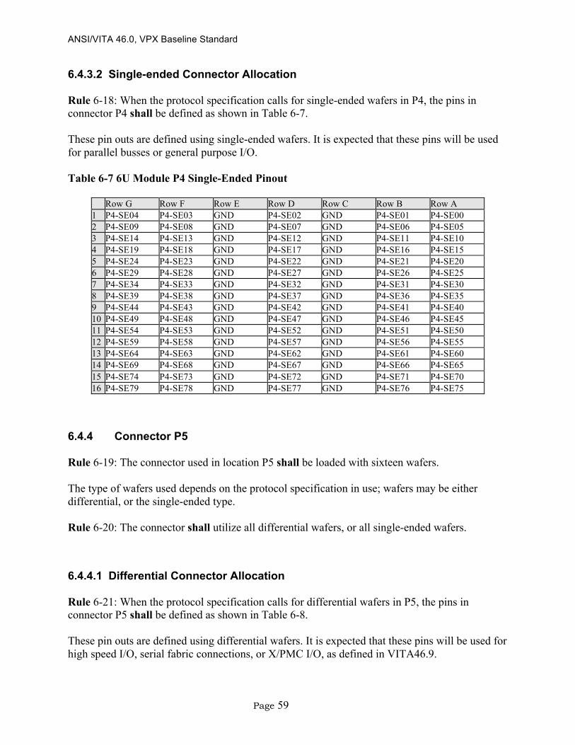
ANSI/VITA 46.0, VPX Baseline Standard
Page 59
6.4.3.2 Single-ended Connector Allocation
Rule 6-18: When the protocol specification calls for single-ended wafers in P4, the pins in connector P4 shall be defined as shown in Table 6-7. These pin outs are defined using single-ended wafers. It is expected that these pins will be used for parallel busses or general purpose I/O. Table 6-7 6U Module P4 Single-Ended Pinout
Row G Row F Row E Row D Row C Row B Row A 1 P4-SE04 P4-SE03 GND P4-SE02 GND P4-SE01 P4-SE00 2 P4-SE09 P4-SE08 GND P4-SE07 GND P4-SE06 P4-SE05 3 P4-SE14 P4-SE13 GND P4-SE12 GND P4-SE11 P4-SE10 4 P4-SE19 P4-SE18 GND P4-SE17 GND P4-SE16 P4-SE15 5 P4-SE24 P4-SE23 GND P4-SE22 GND P4-SE21 P4-SE20 6 P4-SE29 P4-SE28 GND P4-SE27 GND P4-SE26 P4-SE25 7 P4-SE34 P4-SE33 GND P4-SE32 GND P4-SE31 P4-SE30 8 P4-SE39 P4-SE38 GND P4-SE37 GND P4-SE36 P4-SE35 9 P4-SE44 P4-SE43 GND P4-SE42 GND P4-SE41 P4-SE40 10 P4-SE49 P4-SE48 GND P4-SE47 GND P4-SE46 P4-SE45 11 P4-SE54 P4-SE53 GND P4-SE52 GND P4-SE51 P4-SE50 12 P4-SE59 P4-SE58 GND P4-SE57 GND P4-SE56 P4-SE55 13 P4-SE64 P4-SE63 GND P4-SE62 GND P4-SE61 P4-SE60 14 P4-SE69 P4-SE68 GND P4-SE67 GND P4-SE66 P4-SE65 15 P4-SE74 P4-SE73 GND P4-SE72 GND P4-SE71 P4-SE70 16 P4-SE79 P4-SE78 GND P4-SE77 GND P4-SE76 P4-SE75
6.4.4 Connector P5
Rule 6-19: The connector used in location P5 shall be loaded with sixteen wafers. The type of wafers used depends on the protocol specification in use; wafers may be either differential, or the single-ended type. Rule 6-20: The connector shall utilize all differential wafers, or all single-ended wafers.
6.4.4.1 Differential Connector Allocation
Rule 6-21: When the protocol specification calls for differential wafers in P5, the pins in connector P5 shall be defined as shown in Table 6-8. These pin outs are defined using differential wafers. It is expected that these pins will be used for high speed I/O, serial fabric connections, or X/PMC I/O, as defined in VITA46.9.
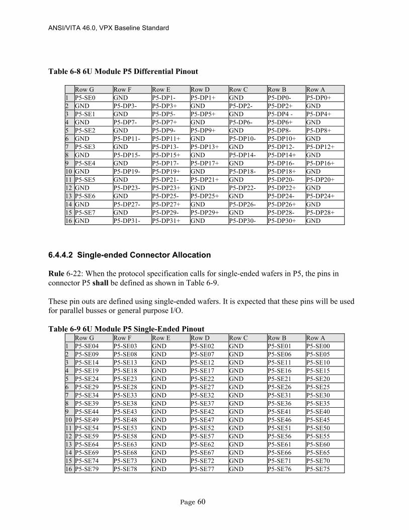
ANSI/VITA 46.0, VPX Baseline Standard
Page 60
Table 6-8 6U Module P5 Differential Pinout
Row G Row F Row E Row D Row C Row B Row A 1 P5-SE0 GND P5-DP1- P5-DP1+ GND P5-DP0- P5-DP0+ 2 GND P5-DP3- P5-DP3+ GND P5-DP2- P5-DP2+ GND 3 P5-SE1 GND P5-DP5- P5-DP5+ GND P5-DP4 - P5-DP4+ 4 GND P5-DP7- P5-DP7+ GND P5-DP6- P5-DP6+ GND 5 P5-SE2 GND P5-DP9- P5-DP9+ GND P5-DP8- P5-DP8+ 6 GND P5-DP11- P5-DP11+ GND P5-DP10- P5-DP10+ GND 7 P5-SE3 GND P5-DP13- P5-DP13+ GND P5-DP12- P5-DP12+ 8 GND P5-DP15- P5-DP15+ GND P5-DP14- P5-DP14+ GND 9 P5-SE4 GND P5-DP17- P5-DP17+ GND P5-DP16- P5-DP16+ 10 GND P5-DP19- P5-DP19+ GND P5-DP18- P5-DP18+ GND 11 P5-SE5 GND P5-DP21- P5-DP21+ GND P5-DP20- P5-DP20+ 12 GND P5-DP23- P5-DP23+ GND P5-DP22- P5-DP22+ GND 13 P5-SE6 GND P5-DP25- P5-DP25+ GND P5-DP24- P5-DP24+ 14 GND P5-DP27- P5-DP27+ GND P5-DP26- P5-DP26+ GND 15 P5-SE7 GND P5-DP29- P5-DP29+ GND P5-DP28- P5-DP28+ 16 GND P5-DP31- P5-DP31+ GND P5-DP30- P5-DP30+ GND
6.4.4.2 Single-ended Connector Allocation
Rule 6-22: When the protocol specification calls for single-ended wafers in P5, the pins in connector P5 shall be defined as shown in Table 6-9. These pin outs are defined using single-ended wafers. It is expected that these pins will be used for parallel busses or general purpose I/O. Table 6-9 6U Module P5 Single-Ended Pinout
Row G Row F Row E Row D Row C Row B Row A 1 P5-SE04 P5-SE03 GND P5-SE02 GND P5-SE01 P5-SE00 2 P5-SE09 P5-SE08 GND P5-SE07 GND P5-SE06 P5-SE05 3 P5-SE14 P5-SE13 GND P5-SE12 GND P5-SE11 P5-SE10 4 P5-SE19 P5-SE18 GND P5-SE17 GND P5-SE16 P5-SE15 5 P5-SE24 P5-SE23 GND P5-SE22 GND P5-SE21 P5-SE20 6 P5-SE29 P5-SE28 GND P5-SE27 GND P5-SE26 P5-SE25 7 P5-SE34 P5-SE33 GND P5-SE32 GND P5-SE31 P5-SE30 8 P5-SE39 P5-SE38 GND P5-SE37 GND P5-SE36 P5-SE35 9 P5-SE44 P5-SE43 GND P5-SE42 GND P5-SE41 P5-SE40 10 P5-SE49 P5-SE48 GND P5-SE47 GND P5-SE46 P5-SE45 11 P5-SE54 P5-SE53 GND P5-SE52 GND P5-SE51 P5-SE50 12 P5-SE59 P5-SE58 GND P5-SE57 GND P5-SE56 P5-SE55 13 P5-SE64 P5-SE63 GND P5-SE62 GND P5-SE61 P5-SE60 14 P5-SE69 P5-SE68 GND P5-SE67 GND P5-SE66 P5-SE65 15 P5-SE74 P5-SE73 GND P5-SE72 GND P5-SE71 P5-SE70 16 P5-SE79 P5-SE78 GND P5-SE77 GND P5-SE76 P5-SE75

ANSI/VITA 46.0, VPX Baseline Standard
Page 61
6.4.5 Connector P6
Rule 6-23: The connector used in location P6 shall be loaded with sixteen wafers. The type of wafers used depends on the protocol specification in use; wafers may be either differential, or the single-ended type. Rule 6-24: The connector shall utilize all differential wafers, or all single-ended wafers.
6.4.5.1 Differential Connector Allocation
Rule 6-25: When the protocol specification calls for differential wafers in P6, the pins in connector P6 shall be defined as shown in Table 6-10. These pin outs are defined using differential wafers. It is expected that these pins will be used for high speed I/O, serial fabric connections, or X/PMC I/O, as defined in VITA46.9. Table 6-10 6U Module P6 Differential Pinout
Row G Row F Row E Row D Row C Row B Row A 1 P6-SE0 GND P6-DP1- P6-DP1+ GND P6-DP0- P6-DP0+ 2 GND P6-DP3- P6-DP3+ GND P6-DP2- P6-DP2+ GND 3 P6-SE1 GND P6-DP5- P6-DP5+ GND P6-DP4 - P6-DP4+ 4 GND P6-DP7- P6-DP7+ GND P6-DP6- P6-DP6+ GND 5 P6-SE2 GND P6-DP9- P6-DP9+ GND P6-DP8- P6-DP8+ 6 GND P6-DP11- P6-DP11+ GND P6-DP10- P6-DP10+ GND 7 P6-SE3 GND P6-DP13- P6-DP13+ GND P6-DP12- P6-DP12+ 8 GND P6-DP15- P6-DP15+ GND P6-DP14- P6-DP14+ GND 9 P6-SE4 GND P6-DP17- P6-DP17+ GND P6-DP16- P6-DP16+ 10 GND P6-DP19- P6-DP19+ GND P6-DP18- P6-DP18+ GND 11 P6-SE5 GND P6-DP21- P6-DP21+ GND P6-DP20- P6-DP20+ 12 GND P6-DP23- P6-DP23+ GND P6-DP22- P6-DP22+ GND 13 P6-SE6 GND P6-DP25- P6-DP25+ GND P6-DP24- P6-DP24+ 14 GND P6-DP27- P6-DP27+ GND P6-DP26- P6-DP26+ GND 15 P6-SE7 GND P6-DP29- P6-DP29+ GND P6-DP28- P6-DP28+ 16 GND P6-DP31- P6-DP31+ GND P6-DP30- P6-DP30+ GND
6.4.5.2 Single-ended Connector Allocation
Rule 6-26: When the protocol specification calls for single-ended wafers in P6, the pins in connector P6 shall be defined as shown in Table 6-11 .
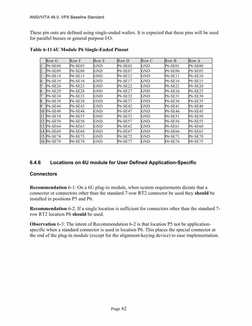
ANSI/VITA 46.0, VPX Baseline Standard
Page 62
These pin outs are defined using single-ended wafers. It is expected that these pins will be used for parallel busses or general purpose I/O. Table 6-11 6U Module P6 Single-Ended Pinout
Row G Row F Row E Row D Row C Row B Row A 1 P6-SE04 P6-SE03 GND P6-SE02 GND P6-SE01 P6-SE00 2 P6-SE09 P6-SE08 GND P6-SE07 GND P6-SE06 P6-SE05 3 P6-SE14 P6-SE13 GND P6-SE12 GND P6-SE11 P6-SE10 4 P6-SE19 P6-SE18 GND P6-SE17 GND P6-SE16 P6-SE15 5 P6-SE24 P6-SE23 GND P6-SE22 GND P6-SE21 P6-SE20 6 P6-SE29 P6-SE28 GND P6-SE27 GND P6-SE26 P6-SE25 7 P6-SE34 P6-SE33 GND P6-SE32 GND P6-SE31 P6-SE30 8 P6-SE39 P6-SE38 GND P6-SE37 GND P6-SE36 P6-SE35 9 P6-SE44 P6-SE43 GND P6-SE42 GND P6-SE41 P6-SE40 10 P6-SE49 P6-SE48 GND P6-SE47 GND P6-SE46 P6-SE45 11 P6-SE54 P6-SE53 GND P6-SE52 GND P6-SE51 P6-SE50 12 P6-SE59 P6-SE58 GND P6-SE57 GND P6-SE56 P6-SE55 13 P6-SE64 P6-SE63 GND P6-SE62 GND P6-SE61 P6-SE60 14 P6-SE69 P6-SE68 GND P6-SE67 GND P6-SE66 P6-SE65 15 P6-SE74 P6-SE73 GND P6-SE72 GND P6-SE71 P6-SE70 16 P6-SE79 P6-SE78 GND P6-SE77 GND P6-SE76 P6-SE75
6.4.6 Locations on 6U module for User Defined Application-Specific
Connectors
Recommendation 6-1: On a 6U plug-in module, when system requirements dictate that a connector or connectors other than the standard 7-row RT2 connector be used they should be installed in positions P5 and P6.
Recommendation 6-2: If a single location is sufficient for connectors other than the standard 7-row RT2 location P6 should be used.
Observation 6-3: The intent of Recommendation 6-2 is that location P5 not be application-specific when a standard connector is used in location P6. This places the special connector at the end of the plug-in module (except for the alignment-keying device) to ease implementation.
ANSI/VITA 46.0, VPX Baseline Standard
Page 63
7 Backplanes
7.1 Overview
7.1.1 Backplane Dimensions
Appendix B provides dimensional information for compliant backplanes. Figure B-1 shows 3U air-cooled systems; Figure B-2, a 6U air-cooled backplane, Figure B-3, a 3U conduction cooled backplane, Figure B-4, a 6U conduction cooled backplane, and finally, Figure B-5 shows the end view of a 6U backplane. Rule 7-1: Backplane slots shall use alignment-keying devices as shown in Appendix B. These devices shall provide a safety ground path from the plug-in module to the backplane and hence to the system safety ground point.
7.1.2 Power Delivery
Rule 7-2: Backplanes shall be documented using the following mnemonic: “VS1:2:3 = x:y:z” where “x”, “y” and “z” are the aggregate rated concurrent current carrying capabilities in amps of Vs1, Vs2 and Vs3 respectively. Recommendation 7-1: Each slot should be capable of concurrently providing 22A on each of Vs1, Vs2 and Vs3. Rule 7-3: The backplane shall be capable of providing up to 1 A per slot for each of the auxiliary voltages: 3.3V_AUX, +12V_AUX, -12V_AUX.
7.1.3 Connector Selection
Rule 7-4: Backplane connectors shall be present in two contiguous strips beginning at J0 and J3, with each strip terminated by a right-end connector. The first contiguous strip can be J0, J1 or J0, J1, J2. The second contiguous strip can be J3 or J3, J4 or J3, J4, J5 or J3, J4, J5, J6. In 3U systems, J2 is optional. In 6U systems, J2, J3, J4, J5 and J6 are optional. Observation 7-1: To completely shroud the connector contacts, the length of the backplane connector strip must match the length of the plug-in module connector strip. However, a plug-in module connector strip that is shorter than a backplane connector strip is mechanically compatible, but not vice-versa. Observation 7-2: It is intended that most COTS backplane slots be populated with J0-J6 connectors corresponding to a fully populated plug-in module, but Rule 7-4 also allows for

ANSI/VITA 46.0, VPX Baseline Standard
Page 64
compliant backplane slots to be tailored for specific applications. (e.g. the removal of optional connectors J5 and J6, where J4 becomes a right-end connector) Observation 7-3: The backplane connectors do not differentiate among power, single-ended and differential wafers. The three backplane connector types are:
1/2 size left end (8 wafers, used for J0 utility connector)25 Center (16 wafers)26 Right end (16 wafers used as the end connector)27
User defined connectors must be compatible with the selected plug-in module connectors.
7.2 VITA 46 slot numbering
Geographic Addressing is required in compliant backplanes and plug-in modules. The following rules define this use for backplanes. Rule 7-5: The leftmost slot (viewed from the plug-in module insertion side with P0 at the top) of a backplane shall have a geographic address of ‘1.’ Rule 7-6: In a compliant backplane, slot numbering starts in Slot1 and continues to Slot ‘n,’ where ‘n’ is the total number of slots. The geographic address shall reflect the slot number so defined. Rule 7-7: The six geographical address pins (GA0*, GA1*, GA2*, GA3*, GA4* and GAP*) shall either be tied to ground with a maximum resistance of 1.0 Ohm, or left open (floating) on the backplane J0 connector as defined in Table 7-1. See Section 4.8.2. Rule 7-8: The sum of grounded geographical address pins (GA0*, GA1*, GA2*, GA3*, GA4*, and GAP*) shall be odd. This is equivalent to odd parity, assuming each grounded pin represents a logic '1'. A full table of legal combinations is presented in Table 7-1.
Rule 7-9: The preceding two rules shall apply to backplanes with only VITA46 slots, to hybrid backplanes using either VME64 or cPCI plug-in modules for legacy slots, and to hybrid backplanes which have these legacy slots on either side of the VITA46 slots, or interspersed among them.
25 Tyco P/N 1410186-1 or equivalent 26 Tyco P/N 1410140-1 or equivalent 27 Tyco P/N 1410142-1 or equivalent
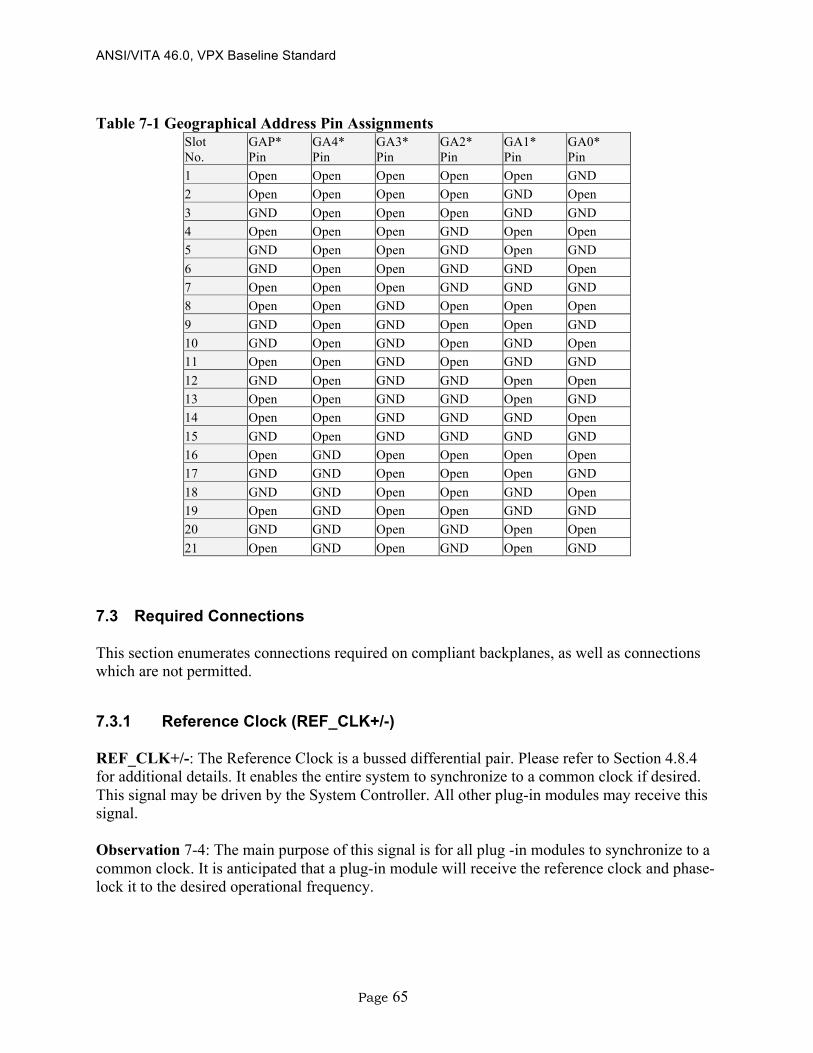
ANSI/VITA 46.0, VPX Baseline Standard
Page 65
Table 7-1 Geographical Address Pin Assignments
Slot No.
GAP* Pin
GA4* Pin
GA3* Pin
GA2* Pin
GA1* Pin
GA0* Pin
1 Open Open Open Open Open GND 2 Open Open Open Open GND Open 3 GND Open Open Open GND GND 4 Open Open Open GND Open Open 5 GND Open Open GND Open GND 6 GND Open Open GND GND Open 7 Open Open Open GND GND GND 8 Open Open GND Open Open Open 9 GND Open GND Open Open GND 10 GND Open GND Open GND Open 11 Open Open GND Open GND GND 12 GND Open GND GND Open Open 13 Open Open GND GND Open GND 14 Open Open GND GND GND Open 15 GND Open GND GND GND GND 16 Open GND Open Open Open Open 17 GND GND Open Open Open GND 18 GND GND Open Open GND Open 19 Open GND Open Open GND GND 20 GND GND Open GND Open Open 21 Open GND Open GND Open GND
7.3 Required Connections
This section enumerates connections required on compliant backplanes, as well as connections which are not permitted.
7.3.1 Reference Clock (REF_CLK+/-)
REF_CLK+/-: The Reference Clock is a bussed differential pair. Please refer to Section 4.8.4 for additional details. It enables the entire system to synchronize to a common clock if desired. This signal may be driven by the System Controller. All other plug-in modules may receive this signal. Observation 7-4: The main purpose of this signal is for all plug -in modules to synchronize to a common clock. It is anticipated that a plug-in module will receive the reference clock and phase-lock it to the desired operational frequency.
ANSI/VITA 46.0, VPX Baseline Standard
Page 66
Rule 7-10: Compliant backplanes shall be designed with the following characteristics: a) Compliant Backplanes shall connect REF_CLK +/- to all slots. b) The Backplane routing of REF_CLK +/- shall support the EIA-899 M-LVDS
technology used by the plug-in modules. The design shall support this interface as a multi-drop bus, with characteristics influenced by plug-in module loading.
c) The differential impedance of REF_CLK+/- on the backplane shall be 130 Ohms ± 10%. These guidelines are derived from simulations for a bussed system topology.
d) The REF_CLK+/- trace lengths within a pair shall be matched such that the signals at the connector shall be matched to better than 8.5 ps.
e) The Backplane differential REF_CLK+/- lines shall be differentially terminated at each end with a resistor of 61.9 Ohms ± 1%.
7.3.2 The System Controller and the SYS_CON Signal
The SYS_CON* signal is a single-ended signal on the backplane which may specify which module is the System Controller (SYS_CON). Please refer to Section 4.8.3 for details. Recommendation 7-2: Standard off-the-shelf backplanes should code the leftmost VITA 46 slot viewed from the faceplate as the System Controller when driven by a plug-in module as per Section 4.8.3. Permission 7-1: Custom backplanes are not restricted to defining slot 1 as the System Controller and may define any slot or device as the System Controller depending on the needs of the system. Observation 7-5: In a hybrid backplane the left most VITA 46 slot might not be physically the left most slot. A series of slots to the left of the left most VITA 46 slots might be VMEbus slots. Observation 7-6: The VITA 46 System Controller function is different than the VME SYSCON function and the two should not be confused.
7.3.3 Bussed Differential Pair, Reserved for Future Use
RES_BUS+/-: This pair is bussed, and Reserved for Future Use.

ANSI/VITA 46.0, VPX Baseline Standard
Page 67
Rule 7-11: Compliant backplanes shall be designed with the following characteristics: a) The RES_BUS+/- pins shall be bussed to all slots on compliant backplanes. b) Shall provide the option to install termination resistors for RES_BUS+/-. Both single-
ended and differential terminations shall be allowed. The termination option shall be available at both ends of the backplane line.
c) The differential impedance of the RES_BUS+/- traces on the Backplane shall be 130 Ohms ± 10%. These guidelines are derived from simulations for a bussed system topology.
d) The trace lengths within a pair shall be matched such that the signals at the connector shall be matched to better than 8.5 ps.
Observation 7-7: The values for single-ended and differential terminations are not defined in this standard as they are beyond the scope of this document. These may be defined in protocol specifications. See Figure 7.1 for the termination network diagram.
Figure 7-1: RES_BUS+/- Backplane Termination
Observation 7-8: If RES_BUS+/- differential signals are used as two single-ended signals beware of the possibility of the cross-talk between RES_BUS+ and RES_BUS- traces due to the differential routing.
7.3.4 JTAG Pin Allocation
This standard allows, on plug-in modules, the use of signals required to implement Test Access Port and Boundary-Scan Architecture, also known as JTAG, specified in IEEE1149.1 or IEEE1149.6. Five pins in J0 are allocated for JTAG. At the writing of this standard, no suitable multi-drop JTAG Standard was codified; therefore, none is specified in this standard. However, recognizing the utility of JTAG implementations in Manufacturing and System test applications, the following is required of compliant backplanes.
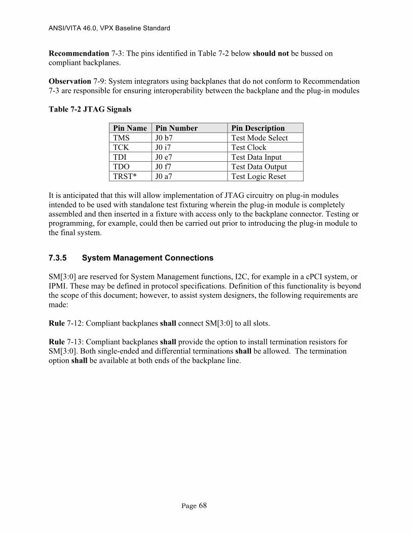
ANSI/VITA 46.0, VPX Baseline Standard
Page 68
Recommendation 7-3: The pins identified in Table 7-2 below should not be bussed on compliant backplanes. Observation 7-9: System integrators using backplanes that do not conform to Recommendation 7-3 are responsible for ensuring interoperability between the backplane and the plug-in modules Table 7-2 JTAG Signals
Pin Name Pin Number Pin Description TMS J0 b7 Test Mode Select TCK J0 i7 Test Clock TDI J0 e7 Test Data Input TDO J0 f7 Test Data Output TRST* J0 a7 Test Logic Reset
It is anticipated that this will allow implementation of JTAG circuitry on plug-in modules intended to be used with standalone test fixturing wherein the plug-in module is completely assembled and then inserted in a fixture with access only to the backplane connector. Testing or programming, for example, could then be carried out prior to introducing the plug-in module to the final system.
7.3.5 System Management Connections
SM[3:0] are reserved for System Management functions, I2C, for example in a cPCI system, or IPMI. These may be defined in protocol specifications. Definition of this functionality is beyond the scope of this document; however, to assist system designers, the following requirements are made: Rule 7-12: Compliant backplanes shall connect SM[3:0] to all slots. Rule 7-13: Compliant backplanes shall provide the option to install termination resistors for SM[3:0]. Both single-ended and differential terminations shall be allowed. The termination option shall be available at both ends of the backplane line.

ANSI/VITA 46.0, VPX Baseline Standard
Page 69
Observation 7-10: This standard does not define timing, frequencies, edge rates, voltages or loading for SM[3:0]. Recommendation 7-4: When SM[3:0] are used to provide an implementation using I2C, the backplane terminations should not be installed. Permission 7-2: Implementation of specific System Management connections is not required. See also Section 4.8.8 for requirements on plug-in modules.
7.3.6 Non-Volatile Memory Read Only
NVMRO: (Non-Volatile Memory Read Only) A system wide signal which, when asserted, prevents any non-volatile memory from being updated. This allows systems with security sensitivity the ability to run classified or sensitive data without the concern that the data will be kept once power has been removed. This also supports the updating or protection of program store memory. This standard does not impose requirements on the source or the timing of this signal. It is expected that it will be created within the system external to the plug-in modules. Rule 7-14: This signal shall be bussed to all slots. Rule 7-15: The backplane shall implement a 5% 220-ohm pull-up resistor to 3.3V_AUX on the bussed NVMRO signal.
Figure 7-2: SM[3:0] Backplane Termination
ANSI/VITA 46.0, VPX Baseline Standard
Page 70
7.3.7 3.3V_AUX
3.3V_AUV is an auxiliary power supply available for plug-in module use. This supply is not intended to provide primary power to the plug-in module, but rather to accommodate system management functionality which might need to operate even if the on-board power conversion circuitry fails. See Section 3.2.2.3.1 for details on this supply. Rule 7-16: The 3.3V_AUX shall supply up to a maximum of 1.0 A per slot.
7.3.8 12V_AUX (+ and -)
Positive and negative 12Volts is provided, with the intent that mezzanine modules requiring this voltage can be accommodated. See Section 3.2.2.3.2 for more details on this power supply. Rule 7-17: The +12V_AUX shall supply up to a maximum of 1.0 A per slot. Rule 7-18: The -12V_AUX shall supply up to a maximum of 1.0 A per slot.
7.3.9 SYSRESET*
This signal is provided to system designers as a method of ensuring that a “clean” start up can occur. Rule 7-19: This signal shall be connected to all slots. Rule 7-20: The backplane shall implement a 5% 220-ohm pull-up resistors to 3.3V_AUX and a 1.8K-ohm pull-down to ground on the SYSRESET* signal, or the Thévenin equivalent implementation, located at each end of the backplane. Observation 7-11: This dual termination is compatible with the ANSI/VITA 1 termination in a hybrid backplane.
7.3.10 P1-RES_BUS_SE
This pin is Reserved for Future Use by VITA 46.0 Base Specification, and bussed on compliant backplanes. Rule 7-21: Compliant backplanes shall be designed with the following characteristics:
a) J1-RES_BUS_SE shall be bussed to all slots. b) Compliant backplanes shall provide the option to install termination resistors for
RES_BUS_SE. Single-ended termination option to 3.3V_AUX and Ground shall be available at both ends of the backplane line
c) The single-ended impedance of the RES_BUS_SE trace shall be 50 ohms.

ANSI/VITA 46.0, VPX Baseline Standard
Page 71
7.3.11 P1-REF_CLK_SE
P1-REF_CLK_SE is reserved for use by subsidiary VITA 46 protocol specifications. Its usage will be defined in those specifications.
7.3.12 P1-VBAT
VBAT is a bussed signal on the VITA 46 backplane. It provides a battery voltage to the plug-in modules. The intent is to supply power to low current devices such as Real Time Clocks when the main power is shut off. Rule 7-22: VBAT shall be a nominal 3V +/- 15% source on the backplane. It shall be bussed to each slot in the backplane. The tracking in the backplane shall allow for at least 1 mA of draw on each backplane slot. Observation 7-12: VBAT is provided for “Battery Backup” purposes, and therefore, may drop as low as the fully discharged battery circuit allows. The system integrator needs to select plug-in modules and a VBAT supply that will meet the intended requirements of their system. Permission 7-3: The power supply, backplane supplier or system integrator may choose to connect 3.3V_AUX to VBAT for those applications that do not need to provide power when the main power is shut off.
7.4 Backplane Fabric Connections Electrical Requirements
It is anticipated that many VITA 46 protocol standards will utilize compatible differential fabric connection topologies, so defining a minimum performance standard for the backplane interconnect will allow the same backplane artwork to be used with many different serial protocols. Recommendation 7-5: Compliant backplanes should be designed to support a signaling rate of at least 3.125 Gbps on any differential point-to-point fabric connection. Permission 7-4: Compliant backplanes may be designed to support higher data rates. Some VITA 46 layered protocol standards may require higher data rates. Observation 7-13: Fabric electrical specifications are found in the applicable subsidiary protocol specifications.
7.5 Hybrid Backplane
This specification does not require that all slots in a backplane be compliant with this base specification.
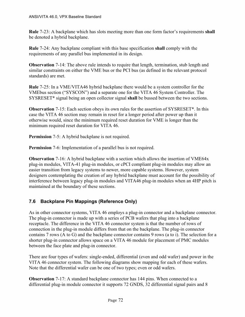
ANSI/VITA 46.0, VPX Baseline Standard
Page 72
Rule 7-23: A backplane which has slots meeting more than one form factor’s requirements shall be denoted a hybrid backplane. Rule 7-24: Any backplane compliant with this base specification shall comply with the requirements of any parallel bus implemented in its design. Observation 7-14: The above rule intends to require that length, termination, stub length and similar constraints on either the VME bus or the PCI bus (as defined in the relevant protocol standards) are met. Rule 7-25: In a VME/VITA46 hybrid backplane there would be a system controller for the VMEbus section (“SYSCON”) and a separate one for the VITA 46 System Controller. The SYSRESET* signal being an open collector signal shall be bussed between the two sections. Observation 7-15: Each section obeys its own rules for the assertion of SYSRESET*. In this case the VITA 46 section may remain in reset for a longer period after power up than it otherwise would, since the minimum required reset duration for VME is longer than the minimum required reset duration for VITA 46. Permission 7-5: A hybrid backplane is not required. Permission 7-6: Implementation of a parallel bus is not required. Observation 7-16: A hybrid backplane with a section which allows the insertion of VME64x plug-in modules, VITA-41 plug-in modules, or cPCI compliant plug-in modules may allow an easier transition from legacy systems to newer, more capable systems. However, system designers contemplating the creation of any hybrid backplane must account for the possibility of interference between legacy plug-in modules and VITA46 plug-in modules when an 4HP pitch is maintained at the boundary of these sections.
7.6 Backplane Pin Mappings (Reference Only)
As in other connector systems, VITA 46 employs a plug-in connector and a backplane connector. The plug-in connector is made up with a series of PCB wafers that plug into a backplane receptacle. The difference in the VITA 46 connector system is that the number of rows of connection in the plug-in module differs from that on the backplane. The plug-in connector contains 7 rows (A to G) and the backplane connector contains 9 rows (a to i). The selection for a shorter plug-in connector allows space on a VITA 46 module for placement of PMC modules between the face plate and plug-in connector. There are four types of wafers: single-ended, differential (even and odd wafer) and power in the VITA 46 connector system. The following diagrams show mapping for each of these wafers. Note that the differential wafer can be one of two types; even or odd wafers. Observation 7-17: A standard backplane connector has 144 pins. When connected to a differential plug-in module connector it supports 72 GNDS, 32 differential signal pairs and 8
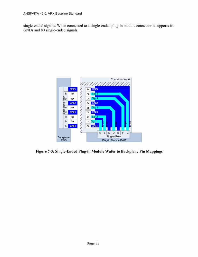
ANSI/VITA 46.0, VPX Baseline Standard
Page 73
single-ended signals. When connected to a single-ended plug-in module connector it supports 64 GNDs and 80 single-ended signals.
Connector Wafer
Backplane PWB
GND
Plug-in Module PWB
ih
g
e
d
f
c
b
a
GNDhx
GND
GND
GND
gx
ex
cx
bx
Back
plan
e Ro
w
GND
Sig 2
bx
cx
dxex
fx
gx
hx
ix
ax
GND
GND
Sig 4
Sig 5
ESD Strip on other sideconnected to GND
to h
x
to g
x
to e
x
t o c
xto
bxSig 1
GFECB DAPlug-in Row
Sig 3
Figure 7-3: Single-Ended Plug-in Module Wafer to Backplane Pin Mappings

ANSI/VITA 46.0, VPX Baseline Standard
Page 74
Figure 7-4: Odd Differential Plug-in Module Wafer to Backplane Pin Mappings
Figure 7-5: Even Differential Plug-in Module Wafer to Backplane Pin Mappings

ANSI/VITA 46.0, VPX Baseline Standard
Page 75
Backplane PWB
Connector Wafer
Plug-in Module PWB
i
h
g
e
d
f
c
b
a
hx
gx
cx
bx
Bac
kpla
ne R
ow
bxcx
dx
fx
gx
hx
ix
ax
Pwr 2
to f,
g,h,
ix
GFECB DAPlug-in Row
ix
fx
ex
dx
ax to a
,b,c
,dx
Pwr 1
Figure 7-6: Power Wafer to Backplane Pin Mappings
The following tables provide a reference allowing readers to map the pin allocations for plug-in modules defined in earlier sections of this standard to the backplane pin allocations, as these are not obvious at first glance. These are not codified by rule, as any compliant connector set will meet these mappings due to the nature of their construction. Table 7-3 J0 (Utility Connector) Backplane Mapping Wafer
Type Row i Row h Row g Row f Row e Row d Row c Row b Row a
1 Power Vs1 Vs1 Vs1 Vs1 None Vs2 Vs2 Vs2 Vs2 2 Power Vs1 Vs1 Vs1 Vs1 None Vs2 Vs2 Vs2 Vs2 3 Power Vs3 Vs3 Vs3 Vs3 None Vs3 Vs3 Vs3 Vs3 4 Single Ended GND SM2 SM3 GND -12V_AUX GND SYSRESET* NVMRO GND 5 Single Ended GND GAP* GA4* GND 3.3V_AUX GND SM0 SM1 GND 6 Single Ended GND GA3* GA2* GND +12V_AUX GND GA1* GA0* GND 7 Odd Diff TCK GND GND TDO TDI GND GND TMS TRST* 8 Even Diff
GND REF_CLK- REF_CLK+ GND GND RES_BUS- RES_BUS+ GND GND

ANSI/VITA 46.0, VPX Baseline Standard
Page 76
Table 7-4 J1 (Differential) Backplane Mapping Row i Row h Row g Row f Row e Row d Row c Row b Row a
1 P1-Res_Bus_SE GND GND P1-DP1- P1-DP1+ GND GND P1-DP0- P1-DP0+
2 GND P1-DP3- P1-DP3+ GND GND P1-DP2- P1-DP2+ GND GND
3 P1-VBAT GND GND P1-DP5- P1-DP5+ GND GND P1-DP4 - P1-DP4+
4 GND P1-DP7- P1-DP7+ GND GND P1-DP6- P1-DP6+ GND GND
5 SYS_CON* GND GND P1-DP9- P1-DP9+ GND GND P1-DP8- P1-DP8+
6 GND P1-DP11- P1-DP11+ GND GND P1-DP10- P1-DP10+ GND GND
7 P1-RFU GND GND P1-DP13- P1-DP13+ GND GND P1-DP12- P1-DP12+
8 GND P1-DP15- P1-DP15+ GND GND P1-DP14- P1-DP14+ GND GND
9 P1-SE4 GND GND P1-DP17- P1-DP17+ GND GND P1-DP16- P1-DP16+
10 GND P1-DP19- P1-DP19+ GND GND P1-DP18- P1-DP18+ GND GND
11 P1-SE5 GND GND P1-DP21- P1-DP21+ GND GND P1-DP20- P1-DP20+
12 GND P1-DP23- P1-DP23+ GND GND P1-DP22- P1-DP22+ GND GND
13 P1-SE6 GND GND P1-DP25- P1-DP25+ GND GND P1-DP24- P1-DP24+
14 GND P1-DP27- P1-DP27+ GND GND P1-DP26- P1-DP26+ GND GND
15 P1-SE7 GND GND P1-DP29- P1-DP29+ GND GND P1-DP28- P1-DP28+
16 GND P1-DP31- P1-DP31+ GND GND P1-DP30- P1-DP30+ GND GND
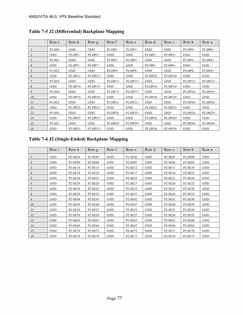
ANSI/VITA 46.0, VPX Baseline Standard
Page 77
Table 7-5 J2 (Differential) Backplane Mapping Row i Row h Row g Row f Row e Row d Row c Row b Row a
1 P2-SE0 GND GND P2-DP1- P2-DP1+ GND GND P2-DP0- P2-DP0+
2 GND P2-DP3- P2-DP3+ GND GND P2-DP2- P2-DP2+ GND GND
3 P2-SE1 GND GND P2-DP5- P2-DP5+ GND GND P2-DP4 - P2-DP4+
4 GND P2-DP7- P2-DP7+ GND GND P2-DP6- P2-DP6+ GND GND
5 P2-SE2 GND GND P2-DP9- P2-DP9+ GND GND P2-DP8- P2-DP8+
6 GND P2-DP11- P2-DP11+ GND GND P2-DP10- P2-DP10+ GND GND
7 P2-SE3 GND GND P2-DP13- P2-DP13+ GND GND P2-DP12- P2-DP12+
8 GND P2-DP15- P2-DP15+ GND GND P2-DP14- P2-DP14+ GND GND
9 P2-SE4 GND GND P2-DP17- P2-DP17+ GND GND P2-DP16- P2-DP16+
10 GND P2-DP19- P2-DP19+ GND GND P2-DP18- P2-DP18+ GND GND
11 P2-SE5 GND GND P2-DP21- P2-DP21+ GND GND P2-DP20- P2-DP20+
12 GND P2-DP23- P2-DP23+ GND GND P2-DP22- P2-DP22+ GND GND
13 P2-SE6 GND GND P2-DP25- P2-DP25+ GND GND P2-DP24- P2-DP24+
14 GND P2-DP27- P2-DP27+ GND GND P2-DP26- P2-DP26+ GND GND
15 P2-SE7 GND GND P2-DP29- P2-DP29+ GND GND P2-DP28- P2-DP28+
16 GND P2-DP31- P2-DP31+ GND GND P2-DP30- P2-DP30+ GND GND
Table 7-6 J2 (Single-Ended) Backplane Mapping Row i Row h Row g Row f Row e Row d Row c Row b Row a
1 GND P2-SE04 P2-SE03 GND P2-SE02 GND P2-SE01 P2-SE00 GND
2 GND P2-SE09 P2-SE08 GND P2-SE07 GND P2-SE06 P2-SE05 GND
3 GND P2-SE14 P2-SE13 GND P2-SE12 GND P2-SE11 P2-SE10 GND
4 GND P2-SE19 P2-SE18 GND P2-SE17 GND P2-SE16 P2-SE15 GND
5 GND P2-SE24 P2-SE23 GND P2-SE22 GND P2-SE21 P2-SE20 GND
6 GND P2-SE29 P2-SE28 GND P2-SE27 GND P2-SE26 P2-SE25 GND
7 GND P2-SE34 P2-SE33 GND P2-SE32 GND P2-SE31 P2-SE30 GND
8 GND P2-SE39 P2-SE38 GND P2-SE37 GND P2-SE36 P2-SE35 GND
9 GND P2-SE44 P2-SE43 GND P2-SE42 GND P2-SE41 P2-SE40 GND
10 GND P2-SE49 P2-SE48 GND P2-SE47 GND P2-SE46 P2-SE45 GND
11 GND P2-SE54 P2-SE53 GND P2-SE52 GND P2-SE51 P2-SE50 GND
12 GND P2-SE59 P2-SE58 GND P2-SE57 GND P2-SE56 P2-SE55 GND
13 GND P2-SE64 P2-SE63 GND P2-SE62 GND P2-SE61 P2-SE60 GND
14 GND P2-SE69 P2-SE68 GND P2-SE67 GND P2-SE66 P2-SE65 GND
15 GND P2-SE74 P2-SE73 GND P2-SE72 GND P2-SE71 P2-SE70 GND
16 GND P2-SE79 P2-SE78 GND P2-SE77 GND P2-SE76 P2-SE75 GND

ANSI/VITA 46.0, VPX Baseline Standard
Page 78
Table 7-7 J3 (Differential) Backplane Mapping Row i Row h Row g Row f Row e Row d Row c Row b Row a
1 P3-SE0 GND GND P3-DP1- P3-DP1+ GND GND P3-DP0- P3-DP0+
2 GND P3-DP3- P3-DP3+ GND GND P3-DP2- P3-DP2+ GND GND
3 P3-SE1 GND GND P3-DP5- P3-DP5+ GND GND P3-DP4 - P3-DP4+
4 GND P3-DP7- P3-DP7+ GND GND P3-DP6- P3-DP6+ GND GND
5 P3-SE2 GND GND P3-DP9- P3-DP9+ GND GND P3-DP8- P3-DP8+
6 GND P3-DP11- P3-DP11+ GND GND P3-DP10- P3-DP10+ GND GND
7 P3-SE3 GND GND P3-DP13- P3-DP13+ GND GND P3-DP12- P3-DP12+
8 GND P3-DP15- P3-DP15+ GND GND P3-DP14- P3-DP14+ GND GND
9 P3-SE4 GND GND P3-DP17- P3-DP17+ GND GND P3-DP16- P3-DP16+
10 GND P3-DP19- P3-DP19+ GND GND P3-DP18- P3-DP18+ GND GND
11 P3-SE5 GND GND P3-DP21- P3-DP21+ GND GND P3-DP20- P3-DP20+
12 GND P3-DP23- P3-DP23+ GND GND P3-DP22- P3-DP22+ GND GND
13 P3-SE6 GND GND P3-DP25- P3-DP25+ GND GND P3-DP24- P3-DP24+
14 GND P3-DP27- P3-DP27+ GND GND P3-DP26- P3-DP26+ GND GND
15 P3-SE7 GND GND P3-DP29- P3-DP29+ GND GND P3-DP28- P3-DP28+
16 GND P3-DP31- P3-DP31+ GND GND P3-DP30- P3-DP30+ GND GND
Table 7-8 J3 (Single-Ended) Backplane Mapping Row i Row h Row g Row f Row e Row d Row c Row b Row a
1 GND P3-SE04 P3-SE03 GND P3-SE02 GND P3-SE01 P3-SE00 GND
2 GND P3-SE09 P3-SE08 GND P3-SE07 GND P3-SE06 P3-SE05 GND
3 GND P3-SE14 P3-SE13 GND P3-SE12 GND P3-SE11 P3-SE10 GND
4 GND P3-SE19 P3-SE18 GND P3-SE17 GND P3-SE16 P3-SE15 GND
5 GND P3-SE24 P3-SE23 GND P3-SE22 GND P3-SE21 P3-SE20 GND
6 GND P3-SE29 P3-SE28 GND P3-SE27 GND P3-SE26 P3-SE25 GND
7 GND P3-SE34 P3-SE33 GND P3-SE32 GND P3-SE31 P3-SE30 GND
8 GND P3-SE39 P3-SE38 GND P3-SE37 GND P3-SE36 P3-SE35 GND
9 GND P3-SE44 P3-SE43 GND P3-SE42 GND P3-SE41 P3-SE40 GND
10 GND P3-SE49 P3-SE48 GND P3-SE47 GND P3-SE46 P3-SE45 GND
11 GND P3-SE54 P3-SE53 GND P3-SE52 GND P3-SE51 P3-SE50 GND
12 GND P3-SE59 P3-SE58 GND P3-SE57 GND P3-SE56 P3-SE55 GND
13 GND P3-SE64 P3-SE63 GND P3-SE62 GND P3-SE61 P3-SE60 GND
14 GND P3-SE69 P3-SE68 GND P3-SE67 GND P3-SE66 P3-SE65 GND
15 GND P3-SE74 P3-SE73 GND P3-SE72 GND P3-SE71 P3-SE70 GND
16 GND P3-SE79 P3-SE78 GND P3-SE77 GND P3-SE76 P3-SE75 GND

ANSI/VITA 46.0, VPX Baseline Standard
Page 79
Table 7-9 J4 (Differential) Backplane Mapping Row i Row h Row g Row f Row e Row d Row c Row b Row a
1 P4-SE0 GND GND P4-DP1- P4-DP1+ GND GND P4-DP0- P4-DP0+
2 GND P4-DP3- P4-DP3+ GND GND P4-DP2- P4-DP2+ GND GND
3 P4-SE1 GND GND P4-DP5- P4-DP5+ GND GND P4-DP4 - P4-DP4+
4 GND P4-DP7- P4-DP7+ GND GND P4-DP6- P4-DP6+ GND GND
5 P4-SE2 GND GND P4-DP9- P4-DP9+ GND GND P4-DP8- P4-DP8+
6 GND P4-DP11- P4-DP11+ GND GND P4-DP10- P4-DP10+ GND GND
7 P4-SE3 GND GND P4-DP13- P4-DP13+ GND GND P4-DP12- P4-DP12+
8 GND P4-DP15- P4-DP15+ GND GND P4-DP14- P4-DP14+ GND GND
9 P4-SE4 GND GND P4-DP17- P4-DP17+ GND GND P4-DP16- P4-DP16+
10 GND P4-DP19- P4-DP19+ GND GND P4-DP18- P4-DP18+ GND GND
11 P4-SE5 GND GND P4-DP21- P4-DP21+ GND GND P4-DP20- P4-DP20+
12 GND P4-DP23- P4-DP23+ GND GND P4-DP22- P4-DP22+ GND GND
13 P4-SE6 GND GND P4-DP25- P4-DP25+ GND GND P4-DP24- P4-DP24+
14 GND P4-DP27- P4-DP27+ GND GND P4-DP26- P4-DP26+ GND GND
15 P4-SE7 GND GND P4-DP29- P4-DP29+ GND GND P4-DP28- P4-DP28+
16 GND P4-DP31- P4-DP31+ GND GND P4-DP30- P4-DP30+ GND GND
Table 7-10 J4 (Single-Ended) Backplane Mapping Row i Row h Row g Row f Row e Row d Row c Row b Row a
1 GND P4-SE04 P4-SE03 GND P4-SE02 GND P4-SE01 P4-SE00 GND
2 GND P4-SE09 P4-SE08 GND P4-SE07 GND P4-SE06 P4-SE05 GND
3 GND P4-SE14 P4-SE13 GND P4-SE12 GND P4-SE11 P4-SE10 GND
4 GND P4-SE19 P4-SE18 GND P4-SE17 GND P4-SE16 P4-SE15 GND
5 GND P4-SE24 P4-SE23 GND P4-SE22 GND P4-SE21 P4-SE20 GND
6 GND P4-SE29 P4-SE28 GND P4-SE27 GND P4-SE26 P4-SE25 GND
7 GND P4-SE34 P4-SE33 GND P4-SE32 GND P4-SE31 P4-SE30 GND
8 GND P4-SE39 P4-SE38 GND P4-SE37 GND P4-SE36 P4-SE35 GND
9 GND P4-SE44 P4-SE43 GND P4-SE42 GND P4-SE41 P4-SE40 GND
10 GND P4-SE49 P4-SE48 GND P4-SE47 GND P4-SE46 P4-SE45 GND
11 GND P4-SE54 P4-SE53 GND P4-SE52 GND P4-SE51 P4-SE50 GND
12 GND P4-SE59 P4-SE58 GND P4-SE57 GND P4-SE56 P4-SE55 GND
13 GND P4-SE64 P4-SE63 GND P4-SE62 GND P4-SE61 P4-SE60 GND
14 GND P4-SE69 P4-SE68 GND P4-SE67 GND P4-SE66 P4-SE65 GND
15 GND P4-SE74 P4-SE73 GND P4-SE72 GND P4-SE71 P4-SE70 GND
16 GND P4-SE79 P4-SE78 GND P4-SE77 GND P4-SE76 P4-SE75 GND

ANSI/VITA 46.0, VPX Baseline Standard
Page 80
Table 7-11 J5 (Differential) Backplane Mapping Row i Row h Row g Row f Row e Row d Row c Row b Row a
1 P5-SE0 GND GND P5-DP1- P5-DP1+ GND GND P5-DP0- P5-DP0+
2 GND P5-DP3- P5-DP3+ GND GND P5-DP2- P5-DP2+ GND GND
3 P5-SE1 GND GND P5-DP5- P5-DP5+ GND GND P5-DP4 - P5-DP4+
4 GND P5-DP7- P5-DP7+ GND GND P5-DP6- P5-DP6+ GND GND
5 P5-SE2 GND GND P5-DP9- P5-DP9+ GND GND P5-DP8- P5-DP8+
6 GND P5-DP11- P5-DP11+ GND GND P5-DP10- P5-DP10+ GND GND
7 P5-SE3 GND GND P5-DP13- P5-DP13+ GND GND P5-DP12- P5-DP12+
8 GND P5-DP15- P5-DP15+ GND GND P5-DP14- P5-DP14+ GND GND
9 P5-SE4 GND GND P5-DP17- P5-DP17+ GND GND P5-DP16- P5-DP16+
10 GND P5-DP19- P5-DP19+ GND GND P5-DP18- P5-DP18+ GND GND
11 P5-SE5 GND GND P5-DP21- P5-DP21+ GND GND P5-DP20- P5-DP20+
12 GND P5-DP23- P5-DP23+ GND GND P5-DP22- P5-DP22+ GND GND
13 P5-SE6 GND GND P5-DP25- P5-DP25+ GND GND P5-DP24- P5-DP24+
14 GND P5-DP27- P5-DP27+ GND GND P5-DP26- P5-DP26+ GND GND
15 P5-SE7 GND GND P5-DP29- P5-DP29+ GND GND P5-DP28- P5-DP28+
16 GND P5-DP31- P5-DP31+ GND GND P5-DP30- P5-DP30+ GND GND
Table 7-12 J5 (Single-Ended) Backplane Mapping Row i Row h Row g Row f Row e Row d Row c Row b Row a
1 GND P5-SE04 P5-SE03 GND P5-SE02 GND P5-SE01 P5-SE00 GND
2 GND P5-SE09 P5-SE08 GND P5-SE07 GND P5-SE06 P5-SE05 GND
3 GND P5-SE14 P5-SE13 GND P5-SE12 GND P5-SE11 P5-SE10 GND
4 GND P5-SE19 P5-SE18 GND P5-SE17 GND P5-SE16 P5-SE15 GND
5 GND P5-SE24 P5-SE23 GND P5-SE22 GND P5-SE21 P5-SE20 GND
6 GND P5-SE29 P5-SE28 GND P5-SE27 GND P5-SE26 P5-SE25 GND
7 GND P5-SE34 P5-SE33 GND P5-SE32 GND P5-SE31 P5-SE30 GND
8 GND P5-SE39 P5-SE38 GND P5-SE37 GND P5-SE36 P5-SE35 GND
9 GND P5-SE44 P5-SE43 GND P5-SE42 GND P5-SE41 P5-SE40 GND
10 GND P5-SE49 P5-SE48 GND P5-SE47 GND P5-SE46 P5-SE45 GND
11 GND P5-SE54 P5-SE53 GND P5-SE52 GND P5-SE51 P5-SE50 GND
12 GND P5-SE59 P5-SE58 GND P5-SE57 GND P5-SE56 P5-SE55 GND
13 GND P5-SE64 P5-SE63 GND P5-SE62 GND P5-SE61 P5-SE60 GND
14 GND P5-SE69 P5-SE68 GND P5-SE67 GND P5-SE66 P5-SE65 GND
15 GND P5-SE74 P5-SE73 GND P5-SE72 GND P5-SE71 P5-SE70 GND
16 GND P5-SE79 P5-SE78 GND P5-SE77 GND P5-SE76 P5-SE75 GND
ANSI/VITA 46.0, VPX Baseline Standard
Page 81
Table 7-13 J6 (Differential) Backplane Mapping Row i Row h Row g Row f Row e Row d Row c Row b Row a
1 P6-SE0 GND GND P6-DP1- P6-DP1+ GND GND P6-DP0- P6-DP0+
2 GND P6-DP3- P6-DP3+ GND GND P6-DP2- P6-DP2+ GND GND
3 P6-SE1 GND GND P6-DP5- P6-DP5+ GND GND P6-DP4 - P6-DP4+
4 GND P6-DP7- P6-DP7+ GND GND P6-DP6- P6-DP6+ GND GND
5 P6-SE2 GND GND P6-DP9- P6-DP9+ GND GND P6-DP8- P6-DP8+
6 GND P6-DP11- P6-DP11+ GND GND P6-DP10- P6-DP10+ GND GND
7 P6-SE3 GND GND P6-DP13- P6-DP13+ GND GND P6-DP12- P6-DP12+
8 GND P6-DP15- P6-DP15+ GND GND P6-DP14- P6-DP14+ GND GND
9 P6-SE4 GND GND P6-DP17- P6-DP17+ GND GND P6-DP16- P6-DP16+
10 GND P6-DP19- P6-DP19+ GND GND P6-DP18- P6-DP18+ GND GND
11 P6-SE5 GND GND P6-DP21- P6-DP21+ GND GND P6-DP20- P6-DP20+
12 GND P6-DP23- P6-DP23+ GND GND P6-DP22- P6-DP22+ GND GND
13 P6-SE6 GND GND P6-DP25- P6-DP25+ GND GND P6-DP24- P6-DP24+
14 GND P6-DP27- P6-DP27+ GND GND P6-DP26- P6-DP26+ GND GND
15 P6-SE7 GND GND P6-DP29- P6-DP29+ GND GND P6-DP28- P6-DP28+
16 GND P6-DP31- P6-DP31+ GND GND P6-DP30- P6-DP30+ GND GND
Table 7-14 J6 (Single-Ended) Backplane Mapping Row i Row h Row g Row f Row e Row d Row c Row b Row a
1 GND P6-SE04 P6-SE03 GND P6-SE02 GND P6-SE01 P6-SE00 GND
2 GND P6-SE09 P6-SE08 GND P6-SE07 GND P6-SE06 P6-SE05 GND
3 GND P6-SE14 P6-SE13 GND P6-SE12 GND P6-SE11 P6-SE10 GND
4 GND P6-SE19 P6-SE18 GND P6-SE17 GND P6-SE16 P6-SE15 GND
5 GND P6-SE24 P6-SE23 GND P6-SE22 GND P6-SE21 P6-SE20 GND
6 GND P6-SE29 P6-SE28 GND P6-SE27 GND P6-SE26 P6-SE25 GND
7 GND P6-SE34 P6-SE33 GND P6-SE32 GND P6-SE31 P6-SE30 GND
8 GND P6-SE39 P6-SE38 GND P6-SE37 GND P6-SE36 P6-SE35 GND
9 GND P6-SE44 P6-SE43 GND P6-SE42 GND P6-SE41 P6-SE40 GND
10 GND P6-SE49 P6-SE48 GND P6-SE47 GND P6-SE46 P6-SE45 GND
11 GND P6-SE54 P6-SE53 GND P6-SE52 GND P6-SE51 P6-SE50 GND
12 GND P6-SE59 P6-SE58 GND P6-SE57 GND P6-SE56 P6-SE55 GND
13 GND P6-SE64 P6-SE63 GND P6-SE62 GND P6-SE61 P6-SE60 GND
14 GND P6-SE69 P6-SE68 GND P6-SE67 GND P6-SE66 P6-SE65 GND
15 GND P6-SE74 P6-SE73 GND P6-SE72 GND P6-SE71 P6-SE70 GND
16 GND P6-SE79 P6-SE78 GND P6-SE77 GND P6-SE76 P6-SE75 GND
7.7 Five Slot Fabric Full Mesh Backplane Routing (Optional – Reference Only)
This standard intentionally does not define routing for a backplane. It does define pin mapping on J1 for 32 differential pairs. This provides flexibility for the system integrator to design the most efficient routing scheme to meet the needs of the application. However, there are standard

ANSI/VITA 46.0, VPX Baseline Standard
Page 82
configurations that can be common to many systems. One of these is a five slot fabric full mesh backplane where the 32 differential pairs on J1 are mapped as 4 differential ports of 4 lanes each. This base standard also does not define protocols to run on the backplanes. These protocols are defined in the “dot” standards. It is highly desirable that a backplane be routed in such a way so as to be useable for many “dot” standards. There are two types of topologies for the protocols, one is a tree like structure like PCIe and the second is a mesh like structure like ASI and SRIO. Tree topologies require a system slot where every other slot is routed to it and full mesh topologies require routing to every other slot. In order to meet the needs of both tree and mesh topologies the following recommendations are made. Recommendation 7-6: The pin mapping of each port should be as shown in Table 7-15. There are four ports labeled PA to PD. Each port has lanes labeled TX0 to TX3 and lanes labeled RX0 to RX3. The TX and RX nomenclature represents the transmit lanes and receive lanes, respectively. This indication of direction is from the daughter card perspective, as a result, the daughter card will inject a signal at the TX locations (backplane rows e-h), and the daughter card will be receptive to signals at the RX locations (backplane rows a-d). Additionally, the naming convention for the actual routes within the backplane may be in contraction to this table, specifically if TX of one card interfaces to the RX of another.
Table 7-15 Recommended Pin Mappings Row i Row h Row g Row f Row e Row d Row c Row b Row a 1 P1-Res_Bus_SE GND GND PA-TX0- PA-TX0+ GND GND PA-RX0- PA-RX0+ 2 GND PA-TX1- PA-TX1+ GND GND PA-RX1- PA-RX1+ GND GND 3 P1-VBAT GND GND PA-TX2- PA-TX2+ GND GND PA-RX2- PA-RX2+ 4 GND PA-TX3- PA-TX3+ GND GND PA-RX3- PA-RX3+ GND GND 5 SYS_CON* GND GND PB-TX0- PB-TX0+ GND GND PB-RX0- PB-RX0+ 6 GND PB-TX1- PB-TX1+ GND GND PB-RX1- PB-RX1+ GND GND 7 P1-RFU GND GND PB-TX2- PB-TX2+ GND GND PB-RX2- PB-RX2+ 8 GND PB-TX3- PB-TX3+ GND GND PB-RX3- PB-RX3+ GND GND 9 P1-SE4 GND GND PC-TX0- PC-TX0+ GND GND PC-RX0- PC-RX0+
10 GND PC-TX1- PC-TX1+ GND GND PC-RX1- PC-RX1+ GND GND 11 P1-SE5 GND GND PC-TX2- PC-TX2+ GND GND PC-RX2- PC-RX2+ 12 GND PC-TX3- PC-TX3+ GND GND PC-RX3- PC-RX3+ GND GND 13 P1-SE6 GND GND PD-TX0- PD-TX0+ GND GND PD-RX0- PD-RX0+ 14 GND PD-TX1- PD-TX1+ GND GND PD-RX1- PD-RX1+ GND GND 15 P1-SE7 GND GND PD-TX2- PD-TX2+ GND GND PD-RX2- PD-RX2+ 16 GND PD-TX3- PD-TX3+ GND GND PD-RX3- PD-RX3+ GND GND

ANSI/VITA 46.0, VPX Baseline Standard
Page 83
Recommendation 7-7: The TX pins of each slot should be connected to the RX pins of the other slots with the routing as shown in Figure 7-7. The following algorithm should be used to wire a five slot full mesh backplane: 1. Start in Slot 1 2. Start from the lowest unwired alpha port, for each unwired port in the slot, wire to each
subsequent slot’s lowest alpha port. 3. Repeat for each slot.
Slot 1 2 3 4 5 A----A B---------A C--------------A D-------------------A B----B C---------B D--------------B C----C D---------C D----D
1A
1B
1D
1C
2A
2B
2D
2C
3A
3B
3C
4A
4B
4D
4C
5A
5B
5D
5C
3D
Figure 7-7 Recommended Port Connection Scheme

ANSI/VITA 46.0, VPX Baseline Standard
Page 84
This backplane routing scheme connects all ports to every other port in a full mesh topology. Slot 1 can also act as the “system slot” in a tree topology (Slot 1 ports connect to port A on each of the other slots).
7.8 Backplane Keying
Refer to section 4.4 for background information and definitions that apply to VITA 46 keying for both plug-in modules and backplanes. Rule 7-26: For 6U backplanes, keying pin #1 shall be keyed in accordance with the High Voltage Power Input provided by the backplane. This keying pin shall be referred to as the voltage keying pin. Observation 7-18: For 3U backplanes keying for input voltage is not required as all prime power inputs have permanently dedicated power wafers, in contrast to the 6U case where either 12V or 48V may be input on the Vs1 and Vs2 power wafers. Recommendation 7-8: For the 6U case, when the High Voltage Power Input supplied by the backplane is 48V, the backplane voltage keying pin should be installed in one of two angular positions - 45 or 90. Recommendation 7-9: For the 6U case, when the High Voltage Power Input supplied by the backplane is 12V, the backplane voltage keying pin should be installed in one of two angular positions - 315 or 0 Observation 7-19: For the 6U case recommendations 7-25 and 7-26 allow for a total range of slot-unique keying of 50 (two key positions on the voltage keying pin, 5 each on keying pins 2 and 3, for a total of 2x5x5 = 50 key settings). Observation 7-20: For the 3U case where both keying positions are used for slot-specific keying there are 25 unique keying assignments possible (5 keying positions on each of keying pins 1 and 2, for a total of 5x5 = 25 key settings). Recommendation 7-10: Standard 6U backplanes should provide angular-alignment holes for the voltage keying pin for at least two angles, either 315 and 45, or 0 and 90. The angular-alignment holes provided for the voltage keying pin should be the same for all the slots positions of the backplane. Observation 7-21: Recommendation7-27 allows a standard 6U backplane to be built that can be keyed for either 12 or 48V. Recommendation 7-11: For the 6U case, the preferred angle for the backplane voltage keying pin for 48V is 45 and this should be used in all cases other than those where there are specific system requirements for a user keying range greater than 25. All standard catalog backplanes should use this setting.

ANSI/VITA 46.0, VPX Baseline Standard
Page 85
Recommendation 7-12: For the 6U case, the preferred angle for the backplane voltage keying pin for 12V is 315 and this should be used in all cases other than those where there are specific system requirements for a user keying range greater than 25. All standard catalog backplanes should use this setting. Recommendation 7-13: For the 6U case, if the backplane does not provide any High Voltage Power Input (Vs1 and Vs2 are no-connects), the voltage keying pin should be installed in one of four angular positions - 0, 45, 90, 315. Recommendation 7-14: For the 6U case, the angular position 270 on the backplane voltage keying pin is Reserved for Future Use. Recommendation 7-15: For the 6U case backplane keying pins #2 and #3 are for slot-specific keying. For the 3U case backplane keying pins #1 and #2 are for slot-specific keying. Recommendation 7-16: To facilitate the application of slot-unique keying by users, standard catalog backplanes should be configured with a unique key setting for each slot on keying pins #2 and #3 for 6U backplanes and #1 and #2 for 3U backplanes. Recommendation 7-17: For 6U backplanes, the standard keying should begin at slot 1 with keying pin #2 set to angle 270 and keying pin #3 set to angle 270. As the slot number increases, the angle of the keying pins should progress with keying pin #2 acting as the "least significant bit" and keying pin #3 acting as the "most significant bit". The sequence of key angles should be 270, 315, 0, 45, 90. I.e., the keying of slot 2 is keying pin #2 set to angle 315, keying pin #3 set to angle 270; the keying of slot 6 is keying pin #2 set to 270, keying pin #3 set to 315. This sequence should continue for as many slots as there are in the backplane. Recommendation 7-18: For 3U backplanes, the standard keying should begin at slot 1 with keying pin #1 set to angle 270 and keying pin #2 set to angle 270. As the slot number increases, the angle of the keying pins should progress with keying pin #1 acting as the "least significant bit" and keying pin #2 acting as the "most significant bit". The sequence of key angles should be 270, 315, 0, 45, 90. I.e., the keying of slot 2 is keying pin #1 set to angle 315, keying pin #2 set to angle 270; the keying of slot 6 is keying pin #1 set to 270, keying pin #2 set to 315. This sequence should continue for as many slots as there are in the backplane. Recommendation 7-19: To provide users with maximum flexibility in adjusting the pre-configured backplane keying if required, as many angular alignment holes as allowable should be provided in the backplane for keying pins #2 and #3 for every slot for the 6U case, and for keying pins #1 and #2 for every slot for the 3U case. Observation 7-22: Except for alignment pin in position #2 on 6U conduction cooled backplanes, here are three recommended part numbers 28 29 30for the backplane alignment and keying pin
28 Tyco part number: 1-1469491-2, or equivalent 29 Tyco part number: 1-1469491-3, or equivalent 30 Tyco part number: 1-1469491-4, or equivalent

ANSI/VITA 46.0, VPX Baseline Standard
Page 86
depending on the backplane thickness. For 6U conduction cooled backplanes, the alignment and keying pin in position #2 changes to a shorter length to meet Rule 7-32. There are three recommended part numbers 31 32 33 for this shorter pin depending on backplane thickness. See manufacturer drawing for dimensions 34
7.9 Preventing Damage from Backwards Plug-in Module Insertion
This section provides requirements and guidance for preventing connector damage resulting from inserting a plug-in module backwards (i.e. 180° around the short axis for 6U, and 180° around the long axis for 3U) into a backplane slot. Observation 7-23: Without preventive measures, backwards 6U plug-in module insertion could result in damage to the P4 connector from alignment-keying pin #2 on a 6U backplane (see Appendix D, Figure D-1). Both air cooled 6U plug-in modules in air cooled chassis and conduction cooled 6U plug-in modules in conduction chassis are affected. Observation 7-24: For the 3U case, there is no middle alignment-keying pin. However, a 3U air cooled plug-in module inserted backwards into a 3U backplane in an air cooled chassis could result in connector damage from the backplane connectors. 3U conduction cooled plug-in modules will not incur connector damage from backwards insertion. This is due to a combination of interference between the alignment-keying pins and sockets, and between the card edge and chassis rail, which stop the plug-in module before the connectors contact one another. Rule 7-27: For 3U and 6U air cooled chassis and backplanes, features shall be included in the chassis and/or the backplane to prevent damage to connectors on 3U and 6U air cooled plug-in modules, respectively, when inserted backwards (i.e. 180° around the short axis). Rule 7-28: For 3U chassis/backplanes, features that meet Rule 7-27 shall stop the backwards inserted plug-in module at a distance of 1.5 to 2.5 mm (0.059” to 0.098”) between the leading edge of the plug-in module connector wafers and the backplane connectors. Rule 7-29: For 6U chassis/backplanes, features that meet Rule 7-27 shall stop the backwards inserted plug-in module at a distance of 1.5 to 2.5 mm (0.059” to 0.098”) between the leading edges of the P4 connector wafers and the alignment pin tip in position #2. Rule 7-30: In order to avoid interference between the specified anti-reversal features and properly inserted plug-in modules, the component height restrictions shown in Figure A-3 (Details A and B) shall be maintained on 6U air cooled plug-in modules.
31 Tyco part number: 1-1410999-2, or equivalent 32 Tyco part number: 1-1410999-3, or equivalent 33 Tyco part number: 1-1410999-4, or equivalent 34 Tyco drawing number: C-1469491, or equivalent
ANSI/VITA 46.0, VPX Baseline Standard
Page 87
Rule 7-31: Features that meet Rule 7-27 shall withstand a force of at least 445 N (100 lbs.), applied to the plug-in module, without yielding. Observation 7-25: See Appendix D (Figures D-2 and D-3) for examples of design concepts for stopping backwards 6U air cooled plug-in module insertion before connector damage occurs. Note that there is no guarantee of performance implied by the use of these concepts. Observation 7-26: Designs that are part of the chassis (e.g. Figure D-2) are preferred so as not to impact backplane space for such features as mounting holes and components. Rule 7-32: For 6U conduction cooled backplanes, the alignment-keying pin in position #2 shall be shorter than the standard pin to prevent P4 connector damage when a 6U conduction cooled plug-in module is inserted backwards. See section 7.8 for recommended part numbers.
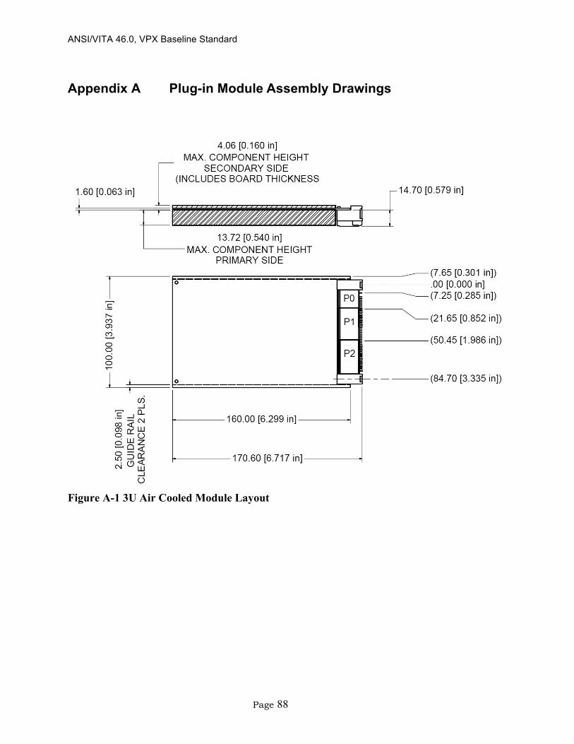
ANSI/VITA 46.0, VPX Baseline Standard
Page 88
Appendix A Plug-in Module Assembly Drawings
Figure A-1 3U Air Cooled Module Layout
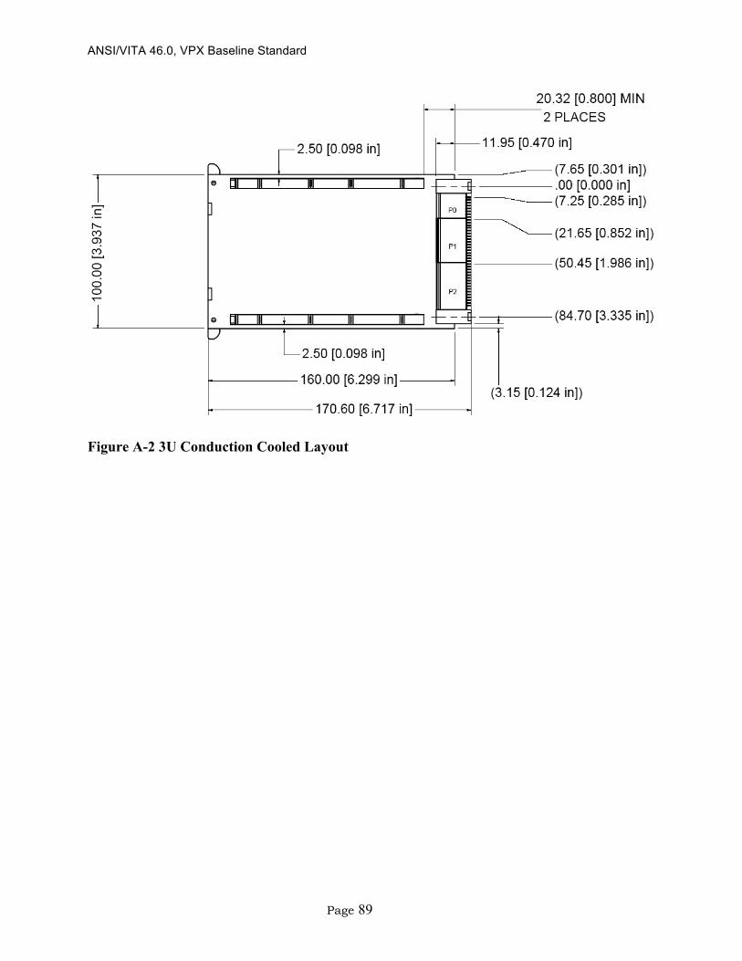
ANSI/VITA 46.0, VPX Baseline Standard
Page 89
Figure A-2 3U Conduction Cooled Layout

ANSI/VITA 46.0, VPX Baseline Standard
Page 90
Figure A-3 6U Air Cooled Layout

ANSI/VITA 46.0, VPX Baseline Standard
Page 91
Figure A-4 6U Conduction Cooled Layout

ANSI/VITA 46.0, VPX Baseline Standard
Page 92
Figure A-5 3U Conduction Cooled Module End View

ANSI/VITA 46.0, VPX Baseline Standard
Page 93
Figure A-6 6U Conduction Cooled Module End View

ANSI/VITA 46.0, VPX Baseline Standard
Page 94
Figure A-7 3U Chassis Side Wall
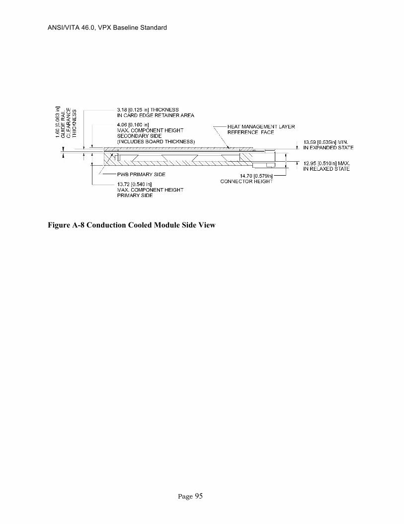
ANSI/VITA 46.0, VPX Baseline Standard
Page 95
Figure A-8 Conduction Cooled Module Side View
ANSI/VITA 46.0, VPX Baseline Standard
Page 96
Appendix B Backplane Printed Circuit Board Fabrication
Drawings
Figure B-1 3U Air Cooled Backplane, Plan View
ANSI/VITA 46.0, VPX Baseline Standard
Page 97
Figure B-2 6U Air Cooled Backplane, Plan View

ANSI/VITA 46.0, VPX Baseline Standard
Page 98
Figure B-3 3U Conduction Cooled Backplane, Plan View

ANSI/VITA 46.0, VPX Baseline Standard
Page 99
Figure B-4 6U Conduction Cooled Backplane, Plan View
ANSI/VITA 46.0, VPX Baseline Standard
Page 100
Figure B-5 6U Backplane, End View

ANSI/VITA 46.0, VPX Baseline Standard
Page 101
Appendix C Plug-in Module Printed Circuit Board Fabrication
Drawings
Figure C-1 3U PCB Fabrication Drawing (viewed from Primary Side)
ANSI/VITA 46.0, VPX Baseline Standard
Page 102
Figure C-2 6U PCB Fabrication Drawing (viewed from Primary Side)
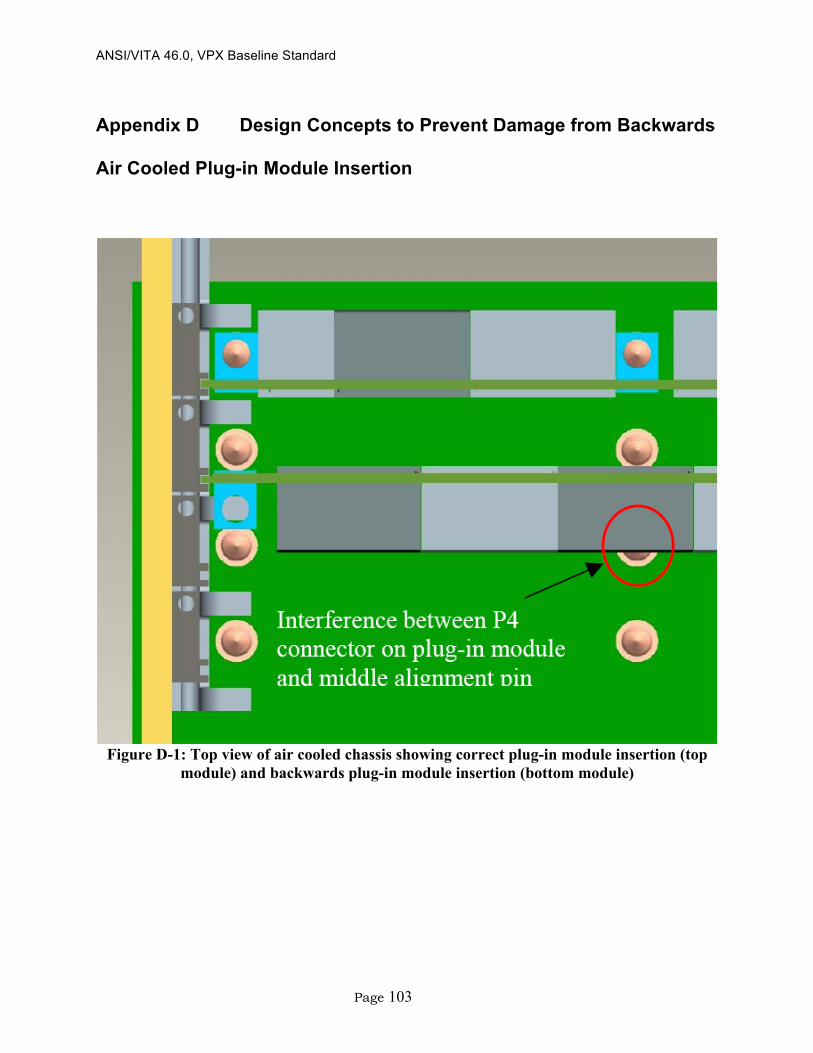
ANSI/VITA 46.0, VPX Baseline Standard
Page 103
Appendix D Design Concepts to Prevent Damage from Backwards
Air Cooled Plug-in Module Insertion
Figure D-1: Top view of air cooled chassis showing correct plug-in module insertion (top
module) and backwards plug-in module insertion (bottom module)
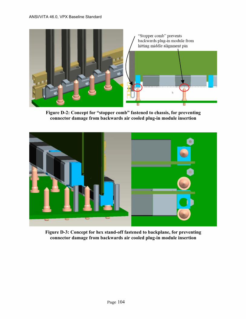
ANSI/VITA 46.0, VPX Baseline Standard
Page 104
Figure D-2: Concept for “stopper comb” fastened to chassis, for preventing
connector damage from backwards air cooled plug-in module insertion
Figure D-3: Concept for hex stand-off fastened to backplane, for preventing
connector damage from backwards air cooled plug-in module insertion