an abstract of a dissertation analysis and control …
TRANSCRIPT
AN ABSTRACT OF A DISSERTATION
ANALYSIS AND CONTROL OF A MICROGRID WITH CONVERTER FED DISTRIBUTED ENERGY SOURCES
Hossein Karimi-Davijani
Doctor of Philosophy in Engineering
The past few decades has seen rapid growth of renewable energy sources for
electric power generation. The main driving forces for this growth are due to the adverse environmental impacts of conventional power plants, their huge costs and losses in long transmission lines. The aforementioned concerns encourage the use of distributed generation (DG) in which the energy sources are installed close to the end users. Renewable energies with their infinite sources (like sun and wind) and the lowest impact on the environment are the first choice for the primary power of distributed generation units.
In a microgrid with renewable energy sources, the objective is to transfer the
maximum possible power. In grid connected mode, since the voltage magnitude and frequency are adapted from the main grid, the controller objectives are different from autonomous operation mode. In grid connected mode the output active and reactive power or input DC–link voltage magnitude can be controlled. In autonomous mode, along with the power balance between the loads and the sources, the voltage magnitude and frequency should be controlled.
To have the same controller strategy in both grid connected and autonomous
modes of operation, the droop control is proposed. To verify the proposed controllers, the dynamic simulation of the system is performed using MATLAB/Simulink and validated through laboratory scale experiment. The designed experimental system consists of a microgrid with two different sources: a nonlinear PV source and a battery source. In addition it includes three different power electronic converters: a unidirectional DC-DC boost converter, a bidirectional buck and boost converter and a three phase inverter. Each converter has its own controller signals coming from different control structure, drivers, sensor boards and digital signal processor (DSP) unit.
Permanent magnet (PM) machines are one of the most popular synchronous
machines in wind turbine applications. In the interior permanent magnet (IPM) structure, the equivalent air gap is not uniform and it makes saliency effect obvious. Therefore, both magnetic and reluctance torque can be produced by IPM machine. In this research the dynamic model of interior permanent magnet machine as a wind turbine generator connected to the grid is studied. The control parts are designed to get maximum power from the wind, keep DC link voltage constant and guarantee unity power factor operation. Loss minimization of the generator is also analyzed. In addition the controllability of the system is studied using the analysis of its open-loop stability and

zero phase behaviors. The zero dynamics of the grid connected IPM generator using both the L and the LCL filter are investigated. The controllability analysis for the IPM generator system suggests that the topological structure of the interface filter and the controlled variables have significant effects on the phase behavior of the system. It is shown that the generator fitted with the L filter has a stable zero dynamics while the system connected though the LCL filter is non-minimum phase.
ANALYSIS AND CONTROL OF A MICROGRID WITH CONVERTER FED
DISTRIBUTED ENERGY SOURCES
__________________________________
A Dissertation
Presented to
The Faculty of the Graduate School
Tennessee Technological University
by
Hossein Karimi-Davijani
__________________________________
In Partial Fulfillment
of the Requirements for the Degree
DOCTOR OF PHILOSOPHY
Engineering
__________________________________
December 2012

ii
CERTIFICATE OF APPROVAL OF DISSERTATION
ANALYSIS AND CONTROL OF A MICROGRID WITH CONVERTER FED
DISTRIBUTED ENERGY SOURCES
by
Hossein Karimi-Davijani
Graduate Advisory Committee:
Joseph O. Ojo, Chairperson Date
Ghadir Radman Date
Ahmed Kamal Date
Omar Elkeelany Date
Yung-Way Liu Date
Approved for the Faculty:
________________________________
Francis Otuonye Associate Vice President for Research and Graduate Studies
________________________________ Date

iii
DEDICATION
To my wife, Shiva and my parents, Parvin and Alireza.

iv
ACKNOWLEDGEMENTS
I would like to express my gratitude to the chairperson of my advisory committee, Dr. Joseph Ojo for his guidance and encouragement during the course of the research. I would like to thank the other members of my committee, Dr. Ghadir Radman, Dr. Omar Elkeelany, Dr. Ahmed Kamal and Dr. Yung-Way Liu for their wonderful courses and their efforts in evaluating my research works.
I would like to thank the office of Center for Energy Systems Research (CESR) and the Department of Electrical and Computer Engineering for the financial support. I also would like to express my gratitude to my lab members, Sosthenes Karugaba, Melaku Mihret, Kennedy Aghana, Dr. Jianfu Fu, Will Mefford, Mehdi Ramezani, Mehdi Khayami, Adineyi Babalola, Bule Mehari and Manideep Angirekula.
I would like to thank my parents for a lifetime support, selfless love, endless patience and encouragement.
Finally, I would like to give my most sincere thanks to my wife Shiva for her moral support, invaluable help and encouragement during the course of my PhD Program.

v
TABLE OF CONTENTS
Page
LIST OF TABLES………….………………...…………………………………....…. .. xiii
LIST OF FIGURES.……..…………………………………………..……………….… xiv
1. INTRODUCTION AND LITERATURE REVIEW ...................................................... 1
1.1 Introduction ........................................................................................................... 1
1.2 Literature Review .................................................................................................. 3
1.2.1 DG Units Control Structures in the Microgrid ........................................... 3
1.2.2 Photovoltaic as a Renewable Source ........................................................ 15
2. CONTROLLER DESIGN, BIFURCATION ANALYSIS AND SIMULATION OF
ISOLATED MICROGRID ............................................................................................... 21
2.1 Introduction ......................................................................................................... 21
2.2 Autonomous Operation of One Converter System .............................................. 23
2.3 Controller Design of One Converter System ...................................................... 27
2.3.1 Droop Control ........................................................................................... 27
2.3.2 Voltage Control ......................................................................................... 29
2.3.3 Current Control ......................................................................................... 31
2.4 Equilibrium Curves of One Converter System .................................................... 36
2.5 Autonomous Operation of Two Converter System ............................................. 40
vi
2.5.1 Dynamic Model ........................................................................................ 41
2.5.2 Controller Unit of Two Converter System ................................................ 44
2.5.3 Droop Control ........................................................................................... 45
2.5.4 Voltage Control ......................................................................................... 47
2.5.5 Current control .......................................................................................... 49
2.5.6 Phase Lock Loop....................................................................................... 52
2.5.7 Simulation of Two Converter System ...................................................... 53
2.6 Conclusion ........................................................................................................... 58
3. STEADY STATE ANALYSIS AND DYNAMIC CONTROL OF PHOTOVOLTAIC
SYSTEM ........................................................................................................................... 59
3.1 Introduction ......................................................................................................... 59
3.2 Dynamic Model of the Stand-Alone System ....................................................... 60
3.2.1 Nonlinear Model and MPP Operation of PV System ............................... 61
3.2.2 Boost Converter Connected to the PV System ......................................... 64
3.2.3 Bidirectional Boost Converter of Battery ................................................. 66
3.2.4 DC Link Equations ................................................................................... 67
3.2.5 Dynamic Model of the Battery ................................................................. 67
3.2.6 Load Equation ........................................................................................... 67
3.2.7 Three Phase Converter Equations ............................................................. 68
3.2.8 Linear Load of DG1 (L1) Equations ......................................................... 68
vii
3.2.9 Capacitor of DG1 Equations ..................................................................... 69
3.3 Steady-State Operation ........................................................................................ 69
3.4 Control Unit Design ............................................................................................ 72
3.4.1 Load Voltage Control ............................................................................... 72
3.4.2 AC Inverter Current Control ..................................................................... 74
3.4.3 PV Voltage Control................................................................................... 76
3.4.4 PV Converter Current Control .................................................................. 77
3.4.5 DC Link Voltage Control.......................................................................... 78
3.4.6 Current Control of Battery Converter ....................................................... 79
3.4.7 Voltage Control of PV in Disabled Battery .............................................. 80
3.4.8 PV Converter Current Control in Disabled Battery .................................. 81
3.4.9 DC Link Voltage Control in Disabled Battery ......................................... 82
3.4.10 Droop Control ........................................................................................... 82
3.4.11 Phase Locked Loop ................................................................................... 84
3.5 Simulation Results ............................................................................................... 86
3.6 Conclusions ......................................................................................................... 89
4. STEADY STATE ANALYSIS AND DYNAMIC CONTROL OF PV SYSTEM
CONNECTED TO THE MAIN GRID ............................................................................. 92
4.1 Introduction ......................................................................................................... 92
4.2 Dynamic Model of the System ............................................................................ 93

viii
4.3 Steady-State Operation ........................................................................................ 97
4.4 Bifurcation Analysis .......................................................................................... 104
4.5 Controller Design .............................................................................................. 110
4.5.1 DC Link Voltage Control........................................................................ 112
4.5.2 Reactive Power Control .......................................................................... 116
4.5.3 Current Control ....................................................................................... 117
4.5.4 State Space Model ................................................................................... 118
4.6 Simulation Results ............................................................................................. 121
4.1 Conclusions ....................................................................................................... 126
5. EXPERIMENTAL SETUP AND DYNAMIC CONTROL OF PV SYSTEM .......... 129
5.1 Introduction ....................................................................................................... 129
5.2 Design and Open Loop Test of the Boost Converter for PV System Applications
129
5.2.1 Input Capacitor Design ........................................................................... 132
5.2.2 The Switch Design .................................................................................. 133
5.2.3 The Diode Design ................................................................................... 134
5.2.4 Output Capacitor Design ......................................................................... 135
5.2.5 The Inductor Design ............................................................................... 135
5.2.6 PCB Model and Open Loop Test of the Boost Converter ...................... 138

ix
5.3 Closed Loop Experimental Design of Maximum Power Point Tracking
Algorithm in PV System Applications ........................................................................... 141
5.3.1 Design of the Current and Voltage Sensors ............................................ 143
5.3.2 Design of the Driver Circuit ................................................................... 145
5.3.3 Design of the Power Supply ................................................................... 148
5.3.4 Controller Design and Closed Loop Test ................................................ 148
5.4 Closed Loop Test of Battery System Converter ................................................ 158
5.5 Design and Open Loop Test of Three Phase Inverter ....................................... 159
5.5.1 Study System .......................................................................................... 160
5.5.2 The Experimental Setup .......................................................................... 166
5.6 Phase Lock Loop ............................................................................................... 168
5.7 Connection of Three Phase Inverter to the Grid ................................................ 172
5.7.1 Study System .......................................................................................... 174
5.7.2 Power Control of Inverter in Grid Connected Mode .............................. 181
5.8 Comparison of PLL and EPLL .......................................................................... 188
5.9 Connection of the PV, Battery and Three Phase Inverter ................................. 209
5.10 Conclusions ....................................................................................................... 215
6. DYNAMIC OPERATION AND CONTROL OF GRID COONECTED INTERIOR
PERMANENT MAGNET WIND TURBINE GENERATOR....................................... 219
6.1 Introduction ....................................................................................................... 219
x
6.2 Study System ..................................................................................................... 221
6.3 Wind Turbine Model ......................................................................................... 222
6.3.1 Defining MPP in Wind Turbine .............................................................. 224
6.3.2 Pitch Angle Effect ................................................................................... 225
6.4 Dynamic Model and Steady State Operation region ......................................... 229
6.4.1 Steady State Operation under Constant Generator Speed after Nominal
Wind Speed 240
6.4.2 Steady state operation under constant pitch angle .................................. 244
6.5 Operation Regions of the Permanent Magnet Machine .................................... 244
6.5.1 Voltage and Current Constraints of PM Machine................................... 248
6.5.2 Maximum Torque per Ampere (MTPA) Operation (ω≤ωb) ................... 251
6.5.3 Maximum Torque per Voltage (MTPV) Operation (Flux Weakening)
(ωb≤ω≤ωc1) 255
6.5.4 Flux Weakening with Stator Current Operation (ω≥ωc1) ....................... 256
6.6 Machine Side Converter Controller Design ...................................................... 261
6.6.1 Loss Minimization and Rotor Speed Control ......................................... 264
6.6.2 Current Control ....................................................................................... 267
6.7 Grid Side Converter Controller Design ............................................................. 270
6.7.1 DC Link Voltage and Reactive Power Control....................................... 270
6.7.2 Current Control ....................................................................................... 273
xi
6.8 Simulation Results ............................................................................................. 274
6.9 Conclusions ....................................................................................................... 275
7. CONTROLLABILITY ANALYSIS OF RENEWABLE ENERGY SOURCES
CONNECTED TO THE GRID ...................................................................................... 279
7.1 Introduction ....................................................................................................... 279
7.2 Zero Dynamics of the Nonlinear System .......................................................... 282
7.2.1 First Method ............................................................................................ 284
7.2.2 Second Method ....................................................................................... 285
7.3 Controllability of Wind Turbine Connected through L filter to the Grid.......... 286
7.3.1 Steady State and Stable Operation Region ............................................. 288
7.3.2 Zero Dynamic Analysis .......................................................................... 292
7.4 Controllability of Wind Turbine Connected through LCL filter to the Grid .... 294
7.4.1 Steady State and Stable Operation Region ............................................. 295
7.4.2 Zero Dynamic Analysis .......................................................................... 301
7.5 Controllability and Stability Analysis of PV System Connected to Current
Source Inverter ................................................................................................................ 308
7.5.1 Steady State and Stability Analysis of the System ................................. 310
7.5.2 Zero Dynamics Analysis of PV .............................................................. 313
7.6 Conclusions ....................................................................................................... 321
8. CONCLUSION AND FUTURE WORKS ................................................................. 323

xii
8.1 Introduction ....................................................................................................... 323
8.2 Conclusions ....................................................................................................... 323
8.3 Future Work ...................................................................................................... 327
REFERENCES ............................................................................................................... 329
APPENDIX ..................................................................................................................... 344
PUBLICATIONS ............................................................................................................ 358
VITA ............................................................................................................................... 359

xiii
LIST OF TABLES
Page
Table 2.1 System parameters of DG ................................................................................. 54
Table 2.2 Parameters of the designed controllers ............................................................. 54
Table 3.1 Parameters of PV system .................................................................................. 62
Table 3.2 Parameters of power system ............................................................................. 86
Table 3.3 Parameters of the battery .................................................................................. 86
Table 3.4 PI controllers’ coefficients ................................................................................ 86
Table 4.1 System parameters of DG connected to the grid .............................................. 98
Table 5.1 Parameters of the designed inductor ............................................................... 137
Table 5.2 Coefficients of the low pass Hamming digital filter ....................................... 154
Table 5.3 The study system parameters .......................................................................... 175
Table 6.1 Wind turbine parameters ................................................................................. 223
Table 6.2 Parameters of the IPM machine and the grid .................................................. 236
Table 6.3Designed parameters of the controllers ........................................................... 271
Table 7.1 Parameters of the IPM machine for controllability analysis........................... 287
xiv
LIST OF FIGURES
Page
Figure 1.1 Different structures of PV system. .................................................................. 18
Figure 2.1 Standalone one converter system schematic diagram ..................................... 23
Figure 2.2 Block diagram of controlled unit beside power stage ..................................... 29
Figure 2.3 Frequency of the system .................................................................................. 36
Figure 2.4 Output active power of converter .................................................................... 37
Figure 2.5 Output reactive power of converter ................................................................. 37
Figure 2.6 Modulation index magnitude of converter ...................................................... 38
Figure 2.7 Load voltage magnitude .................................................................................. 38
Figure 2.8 Active power of linear RL load ....................................................................... 39
Figure 2.9 Reactive power of linear RL load .................................................................... 39
Figure 2.10 Schematic diagram of study system .............................................................. 41
Figure 2.11 Control unit diagram ...................................................................................... 44
Figure 2.12 Droop control unit ......................................................................................... 46
Figure 2.13 Schematic diagram of voltage control and inner current control units ......... 48
Figure 2.14 Block diagram of phase locked loop ............................................................. 52
Figure 2.15 Active and reactive powers reference of first and second converters constant
load, (a) and (b) are active and reactive powers of DG1 constant load, (c) and (d) are
active and reactive powers of DG2 constant load. .................................................... 55

xv
Figure 2.16 Output active and reactive powers of first and second converters, (a) and (b)
are active and reactive powers of DG1, (c) and (d) are active and reactive powers of
DG2. .......................................................................................................................... 55
Figure 2.17 Actual local frequency (blue) and reference frequency (red) of the system, a)
local frequency of DG1, b) local frequency of DG2 ................................................. 56
Figure 2.18 Local load voltages, a) q-axis load voltage of DG1, b) d-axis load voltage of
DG1, c) q-axis load voltage of DG2, d) d-axis load voltage of DG2. ...................... 57
Figure 2.19 Modulation indices of converters, a) q-axis modulation index of first
converter, b) d-axis modulation index of first converter, c) q-axis modulation index
of second converter, d) d-axis modulation index of second converter. .................... 57
Figure 3.1 Schematic diagram of the stand-alone PV, battery inverter power system. .... 61
Figure 3.2 Current and power characteristics of PV system in per unit ........................... 63
Figure 3.3 PV curve characteristics in different irradiation level ..................................... 65
Figure 3.4 Calculated optimum voltage at MPP in different irradiation level .................. 65
Figure 3.5 DC link voltage versus active power of constant load, blue(S = 1), red(S = 0.7)
................................................................................................................................... 70
Figure 3.6 Battery voltage versus active power of constant load, blue (S = 1), red(S = 0.7)
................................................................................................................................... 70
Figure 3.7 Inverter output active power versus active power of constant load, blue(S =1),
red(S = 0.7) ............................................................................................................... 70
Figure 3.8 Inverter output reactive power versus active power of constant load,
blue(S=1), red(S = 0.7) ............................................................................................. 70

xvi
Figure 3.9 Battery output current versus active power of constant load, blue(S= 1), red(S
= 0.7) ......................................................................................................................... 71
Figure 3.10 Battery output power versus active power of constant load, blue( S = 1),
red(S = 0.7) ............................................................................................................... 71
Figure 3.11 PV converter modulation index versus active power of constant load,
blue(M=0.91), red(M=0.61) ...................................................................................... 71
Figure 3.12 Battery converter modulation index versus active power of constant load,
blue(M=0.91), red(M=0.61) ...................................................................................... 71
Figure 3.13 Block diagram of DC-AC three phase converter control part ....................... 73
Figure 3.14 Block diagram of PV DC-DC boost converter control part .......................... 76
Figure 3.15 Block diagram of Battery DC-DC converter control part ............................. 79
Figure 3.16 Block diagram of PV DC-DC boost converter control part if battery converter
is disabled .................................................................................................................. 81
Figure 3.17 Droop control unit ......................................................................................... 82
Figure 3.18 Block diagram of phase locked loop ............................................................. 85
Figure 3.19 Constant load and inverter output active powers .......................................... 87
Figure 3.20 Battery converter modulation index .............................................................. 87
Figure 3.21 Battery output current .................................................................................... 87
Figure 3.22 DC link voltage.............................................................................................. 87
Figure 3.23 PV system output current .............................................................................. 88
Figure 3.24 Inverter modulation index magnitude ........................................................... 88
Figure 3.25 PV converter modulation index ..................................................................... 88
Figure 3.26 Load voltage magnitude ................................................................................ 88

xvii
Figure 3.27 Operation under different irradiation level. (a) irradiation level, (b) reference
and actual PV voltage, (c) PV output current, (d) battery output current, (e) Dc link
voltage ....................................................................................................................... 90
Figure 4.1 Schematic diagram of a DG system with PV source connected to the grid .... 93
Figure 4.2 Nonlinear characteristic of PV source ............................................................. 99
Figure 4.3 Load and capacitor voltage ............................................................................ 100
Figure 4.4 Modulation index magnitude ......................................................................... 100
Figure 4.5 Active power of the main grid (negative means power flows into the main
grid) ......................................................................................................................... 101
Figure 4.6 Reactive power of the main grid ................................................................... 101
Figure 4.7 Reactive power of the converter .................................................................... 101
Figure 4.8 Modulation index magnitude of converter .................................................... 102
Figure 4.9 Load and capacitor voltage ............................................................................ 102
Figure 4.10 q-axis voltage of main grid .......................................................................... 102
Figure 4.11 d-axis voltage of main grid .......................................................................... 102
Figure 4.12 Active power of main grid ........................................................................... 103
Figure 4.13 Reactive power of main grid ....................................................................... 103
Figure 4.14 q-axis output converter current .................................................................... 103
Figure 4.15 Output converter current magnitude ............................................................ 103
Figure 4.16 Equilibrium curve of PV DC voltage when constant load active power (P1) is
an active parameter for different q-axis modulation indices. H (Hopf Bifurcation
Point), LP (Limit Point). ......................................................................................... 105

xviii
Figure 4.17 Equilibrium curve of the main grid active power (Ps) when constant load
active power (P1) is an active parameter for different q-axis modulation indices. 105
Figure 4.18 Equilibrium curve of the main grid reactive power (Qs) when constant load
active power (P1) is an active parameter for different q-axis modulation indices. 106
Figure 4.19 Equilibrium curve of the input power (Pin) when constant load active power
(P1) is an active parameter for different q-axis modulation indices. ...................... 106
Figure 4.20 Equilibrium curve of the load voltage magnitude when constant load active
power (P1) is an active parameter for different q-axis modulation indices. ........... 107
Figure 4.21 Equilibrium curve of the total load active power when constant load active
power (P1) is an active parameter for different q-axis modulation indices. ........... 107
Figure 4.22 Equilibrium curve of the total load reactive power when constant load active
power (P1) is an active parameter for different q-axis modulation indices. ........... 108
Figure 4.23 Equilibrium curve of the per unit q-axis load voltage (Vqm) when constant
load active power (P1) is an active parameter for different q-axis modulation indices.
................................................................................................................................. 108
Figure 4.24 Equilibrium curve of the converter output voltage magnitude when constant
load active power (P1) is an active parameter for different q-axis modulation indices.
................................................................................................................................. 109
Figure 4.25 Block diagram of DC voltage and reactive power control .......................... 113
Figure 4.26 Block diagram of DC voltage and reactive power control after removing the
effect of PV source .................................................................................................. 115
Figure 4.27 Change irradiation level and DC link voltage response for MPPT of PV ... 122

xix
Figure 4.28 Change of active reactive power of the inverter due to the change of
irradiation level ....................................................................................................... 122
Figure 4.29 Change of active reactive power of the main grid due to the change of
irradiation level ....................................................................................................... 123
Figure 4.30 Reference and actual qd-axis currents of inverter ....................................... 123
Figure 4.31 qd-axis modulation indices of the inverter .................................................. 124
Figure 4.32 system dynamic under the change of constant load, a) constant load active
power, b)constant load reactive power, c) active power of the main grid, d) reactive
power of the main grid, e) reactive power of the inverter f) q-axis load voltage g) d-
axis load voltage h) DC link voltage. ...................................................................... 127
Figure 5.1 Schematic diagram of a boost converter ....................................................... 131
Figure 5.2 The actual shape and PCB model of the capacitor ALS30. .......................... 132
Figure 5.3 The actual shape and PCB model of the MOSFET FCH76N60NF. ............. 133
Figure 5.4 The actual shape and PCB model of the diode STTH30L06. ....................... 134
Figure 5.5 The designed inductor ................................................................................... 139
Figure 5.6 Input and output voltage in 50kHz switching frequency and duty ratio of 0.5
................................................................................................................................. 139
Figure 5.7 PCB design of Boost converter circuit a) top layer, b) bottom layer ............ 140
Figure 5.8 Designed PV boost converter ........................................................................ 142
Figure 5.9 Experimental open circuit test of the Boost converter .................................. 142
Figure 5.10 Designed PCB board for current sensor ...................................................... 144
Figure 5.11 Designed PCB board for voltage sensor ...................................................... 144
Figure 5.12 Designed PCB board for driver of the MOSFET ........................................ 145

xx
Figure 5.13 The output of TLP250 driver under the load ............................................... 147
Figure 5.14 The output of UCC27134 driver and IL710 isolator under the load .......... 147
Figure 5.15 The output of MC33151 driver and IL710 isolator under the load ............. 149
Figure 5.16 Designed PCB board for the power supply ................................................. 149
Figure 5.17 Output voltage ripple of the boost converter in terms of change of duty ratio
in any predefine duty ratio set point........................................................................ 151
Figure 5.18 Programmed current versus voltage characteristic of experimental PV source
................................................................................................................................. 152
Figure 5.19 Programmed output power versus voltage characteristic of experimental PV
source ...................................................................................................................... 152
Figure 5.20 Change of duty ratio versus output power of PV system connected to linear
resistive load ........................................................................................................... 153
Figure 5.21 Schematic of the P&O algorithm for MPPT of the PV system ................... 154
Figure 5.22 The experimental setup of the Boost converter for PV MPPT .................... 155
Figure 5.23 Experimental dynamic behavior of the load voltage of PV system using P&O
MPP algorithm ........................................................................................................ 156
Figure 5.24 Experimental steady state operation of the input power versus PV voltage in
MPPT ...................................................................................................................... 156
Figure 5.25 The output of the driver at 50kHz and duty ratio of 0.24 ............................ 157
Figure 5.26 Experimental dynamic behavior of the load voltage of PV with step change
of irradiation level ................................................................................................... 157
Figure 5.27 the bidirectional battery converter ............................................................... 158

xxi
Figure 5.28 Experimental closed loop response of the bidirectional converter, Ch1: Vin,
Ch3:Vdc .................................................................................................................. 159
Figure 5.29 Three phase inverter simulated in MATLAB connected to the load ........... 160
Figure 5.30 Experimental switching signals of produced by DSP in typical SPWM
converter ................................................................................................................. 162
Figure 5.31 Modulation waveform after adding zero sequence to the typical SPWM in
DSP ......................................................................................................................... 164
Figure 5.32 Phase voltage of the inverter using imported DSP SPWM switching signals
................................................................................................................................. 164
Figure 5.33 Phase voltage of the simulated capacitor using imported DSP SPWM
switching signals ..................................................................................................... 165
Figure 5.34 Designed interface circuit to connect the DSP to the inverter drivers ........ 165
Figure 5.35 Experimental set up of the three phase inverter and interface driver circuit 166
Figure 5.36 Experimental inverter output phase voltage of a resistive load with input DC
voltage of 200V and modulation index M=0.8 ....................................................... 167
Figure 5.37 Experimental inverter output phase voltage and phase current of a RL load
with input DC voltage of 200V and modulation index M=0.8 ............................... 167
Figure 5.38 PLL system diagram in the experiment ....................................................... 168
Figure 5.39 Experimental PLL measured frequency and angle of the sample voltage .. 173
Figure 5.40 Original and reproduced voltage from the PLL angle and frequency ......... 173
Figure 5.41 Transformed qd-axis of the sample voltage using PLL angle ..................... 174
Figure 5.42 Three phase inverter connected to the grid and resistive load. .................... 175
Figure 5.43 Single line diagram of the study system in connection to the grid. ............. 177

xxii
Figure 5.44 Designed PCB board for AC voltage sensor. .............................................. 177
Figure 5.45 The measure angular frequency of the grid using PLL ............................... 178
Figure 5.46 The measured line to line grid voltage transformed to qd-axis ................... 178
Figure 5.47 Schematic diagram of AC current sensor .................................................... 179
Figure 5.48 PCB board of three AC current sensors. ..................................................... 180
Figure 5.49 Experimental measured voltages on two sides of the switch before
connection. ( Ch1: Vm1 Ch4:Vm2 Ch3:Is1c) ................................................... 180
Figure 5.50 Effect of dead-time in a fixed frequency and different Vdc and Ma ............ 181
Figure 5.51 Reduced dead-time in the output of DSP PWM signals to 2μs ................... 182
Figure 5.52 Experimental measured open loop voltages after applying correction. ( Ch1:
Vm1 Ch4:Vm2 Ch3:Is1c) .................................................................................. 182
Figure 5.53 Inverter current control structure ................................................................. 184
Figure 5.54 The experimental grid voltage (Ch1) and inverter output phase current (Ch3),
VarQWP refref 5,50 .............................................................................................. 186
Figure 5.55 The experimental grid voltage (Ch1) and inverter output phase current (Ch3),
VarQWP refref 10,100 ............................................................................................... 186
Figure 5.56 Experimental active and reactive power of the inverter in closed loop control.
(Vdc=100 V and Vm1-rms=36 V) ............................................................................... 187
Figure 5.57 Experimental active and reactive power of the inverter at higher voltage.
(Vdc=200 V and Vm1-rms=90 V) ............................................................................... 187
Figure 5.58 Harmonic spectrum of line to line inverter voltage at fsw=5KHz, fundamental
frequency is 20 times reduced scale. ....................................................................... 189
xxiii
Figure 5.59 Harmonic spectrum of line to line inverter voltage at fsw=4860 Hz,
fundamental frequency is 20 times reduced scale. .................................................. 189
Figure 5.60 EPLL system diagram ................................................................................. 195
Figure 5.61 EPLL structure for three phase system ........................................................ 197
Figure 5.62 Experimental output voltage of digital filter ............................................... 203
Figure 5.63 Experimental output voltage of EPLL ......................................................... 204
Figure 5.64 Experimental output current of digital filter ................................................ 204
Figure 5.65 Experimental output current of EPLL ......................................................... 205
Figure 5.66 Experimental qd-axis voltage output of PLL and EPLL ............................. 205
Figure 5.67 Experimental qd-axis voltage output of PLL and EPLL ............................. 206
Figure 5.68 Experimental voltage frequency output of PLL and EPLL ......................... 206
Figure 5.69 Harmonic spectrum of phase current of the digital filter for PLL, fundamental
frequency is 20 times reduced scale. ....................................................................... 207
Figure 5.70 Harmonic spectrum of output phase current of EPLL, fundamental frequency
is 20 times reduced scale. ........................................................................................ 207
Figure 5.71 Hardware experimental setup ...................................................................... 208
Figure 5.72 Relay driver PCB board ............................................................................... 208
Figure 5.73 Experimental closed loop inverter voltage and current controller response 210
Figure 5.74 Experimental active and reactive power of the inverter in both autonomous
and grid connected modes. ...................................................................................... 210
Figure 5.75 Experimental active and reactive power of the grid in both autonomous and
grid connected modes. ............................................................................................ 212
xxiv
Figure 5.76 Experimental active and reactive power of the grid in both autonomous and
grid connected modes. ............................................................................................ 212
Figure 5.77 Experimental qd-axis load voltages in both autonomous and grid connected
modes. ..................................................................................................................... 213
Figure 5.78 Experimental qd-axis inverter currents in both autonomous and grid
connected modes. .................................................................................................... 213
Figure 5.79 Experimental voltage and current of the inverter with changing of the PV
source in grid connected mode, Ch1: Vmab, Ch3:Is1a ......................................... 214
Figure 5.80 Experimental DC-link voltage after connection to the grid and change of
reference power ....................................................................................................... 214
Figure 5.81 Experimental output voltage and current of the PV source ......................... 216
Figure 5.82 Experimental output voltage and current of the battery source ................... 216
Figure 6.1 Schematic diagram of IPM wind turbine connected to the main grid ........... 221
Figure 6.2 Power coefficient versus tip speed ratio at zero pitch angle ......................... 226
Figure 6.3 Power coefficient versus tip speed ratio at zero pitch angle ......................... 226
Figure 6.4 Tip speed ratio versus power coefficient at different pitch angle ................. 228
Figure 6.5 Output power of wind turbine versus generator rotor speed at different pitch
angle and Vw=10(m/s) ............................................................................................ 228
Figure 6.6 Pitch angle versus generator rotor speed at constant turbine power and wind
speed ....................................................................................................................... 229
Figure 6.7 Wind speed versus pitch angle at the rated output power and rated rotor speed
................................................................................................................................. 230
Figure 6.8 Equivalent circuits of IPM Machine .............................................................. 236

xxv
Figure 6.9 Wind turbine speed versus wind speed ......................................................... 241
Figure 6.10 Machine side converter modulation index versus wind speed .................... 241
Figure 6.11 qd-axis stator current magnitudes versus wind speed ................................. 242
Figure 6.12 Stator voltage and current magnitude versus wind speed ........................... 242
Figure 6.13 Power of wind turbine and output active power of generator versus wind
speed ....................................................................................................................... 243
Figure 6.14 Efficiency versus wind speed ...................................................................... 243
Figure 6.15 Wind turbine speed versus wind speed ....................................................... 245
Figure 6.16 Stator voltage and current magnitude versus wind speed ........................... 245
Figure 6.17 Converter modulation index versus wind speed .......................................... 246
Figure 6.18 Power of wind turbine and output active power of generator versus wind
speed ....................................................................................................................... 246
Figure 6.19 Efficiency versus wind speed ...................................................................... 247
Figure 6.20 Power and torque characteristics of PM machine ....................................... 247
Figure 6.21 Voltage and current constraints characteristics a) Interior permanent magnet
machine b) Surface mounted permanent magnet machine ..................................... 250
Figure 6.22 Operation region of PM machine a) Interior permanent magnet machine
( max/ ssdm IL ), b) Interior permanent magnet machine ( max/ ssdm IL ), c) Surface
mounted permanent magnet machine. .................................................................... 257
Figure 6.23 The qd-axis and magnitude of the IPM stator current ................................. 260
Figure 6.24 The qd-axis and magnitude of the IPM stator voltage ................................ 260
Figure 6.25 The output power and torque of the IPM generator .................................... 261
Figure 6.26 Machine side converter controller ............................................................... 265

xxvi
Figure 6.27 Grid side converter controller ...................................................................... 271
Figure 6.28 Dynamic operation of generator and MSC. a) wind speed, b) generator rotor
speed, c) output active power, d) stator current magnitude .................................... 276
Figure 6.29 Pitch angle and power coefficient of wind turbine. a) pitch angle, b) power
coefficient ............................................................................................................... 276
Figure 6.30 Dynamic operation of grid side converter. a) Dc link voltage, b) output
reactive power, c) GSC output current magnitude .................................................. 277
Figure 7.1 Schematic diagram of IPM wind turbine connected to the main grid with L
type filter. ................................................................................................................ 286
Figure 7.2 Steady state operation region of the system. a) output active power of the
generator (W), b) output reactive power of the generator (Var), c) stator current (A),
d) stator voltage (V), e) modulation index magnitude of machine side converter f)
modulation index magnitude of grid side converter ............................................... 290
Figure 7.3 Stability region based on Routh–Hurwitz criteria. The last coefficient of the
characteristic equation............................................................................................. 293
Figure 7.4 The IPM machine as a wind turbine generator connected through LCL filter.
................................................................................................................................. 294
Figure 7.5 Output active power of IPM generator. ......................................................... 296
Figure 7.6 Output reactive power of IPM generator. ...................................................... 296
Figure 7.7 Stator current magnitude of IPM generator. .................................................. 297
Figure 7.8 Stator voltage magnitude of IPM generator. ................................................. 297
Figure 7.9 Modulation index magnitude of the machine side inverter. .......................... 298
Figure 7.10 Modulation index magnitude of the grid side inverter. ............................... 298

xxvii
Figure 7.11 Active power flowing into the grid. ............................................................ 299
Figure 7.12 Two of the coefficients of the linearized zero dynamics characteristic
equation (46). (a) the last coefficient (n0), (b) second coefficient (n2). .................. 308
Figure 7.13 An IPM machine as a wind turbine generator connected through LCL filter.
................................................................................................................................. 309
Figure 7.14 PV output voltage at MPP with in different irradiation level ...................... 313
Figure 7.15 PV output current at MPP with in different irradiation level ...................... 313
Figure 7.16 Inverter modulation index magnitude at different irradiation level ............ 313
Figure 7.17 q-axis capacitor voltage at different irradiation level .................................. 313
Figure 7.18 Two of the coefficients of the linearized PV zero dynamics characteristic 320

1
CHAPTER 1
1.INTRODUCTION AND LITERATURE REVIEW
1.1 Introduction
The environmental effects and the cost of central power plants are causing a large
focus on renewable energies. The power plants are using fossil fuels which result in
greenhouse gas emissions. These greenhouse gas emissions have a significant effect on
the planet especially with the growth of the population and the corresponding increase of
energy consumption. The power plants need to send the electricity to the customers using
long transmission and distribution lines because they have been installed concentrated in
one place and also out of the big cities. A lot of power is lost along the lines which
creates the need for power substations to increase the voltage level at the point of
transmission and reduce it at the point of consumption to minimize these losses. In
addition to the environmental issues, the sources of fossil fuels are limited and depleting
quickly.
The aforementioned concerns encourage the use of distributed generation (DG)
with which the energy sources are installed close to the end users. In particular, for
consumers that are far from the transmission lines or main power plants and small
customers for whom sending energy using transmission lines is not economical, use of
DGs are recommended.
Renewable energies with their essentially infinite source (like sun and wind) and
low impact on the environment are the first choice for the primary power of distribution

2
generation units. Thus the distribution generation can be combined with renewable
energies as their sources to get both the advantages of environmental friendliness and
cost effectiveness. The types of Distributed Generation (DG) units based on renewable
energy which have the fastest growing amount of usage are employing either
photovoltaic cells or wind turbine sources, the choice of which is based on availability,
location, amount of power needed, and feasibility.
When we choose a renewable energy as our input source, we need to consider the
fact that it is typically unpredictable and uncontrollable; therefore, to use these kinds of
sources either in connection to the main grid, or in feeding local loads, the concept of
control and power electronic inverters as an interface should be kept in mind.
Wind turbines produce AC voltage using different kinds of generators and are
normally connected with an AC-DC-AC back-to-back inverter. In this condition, the
input AC voltage is converted to DC voltage and is then converted to an AC voltage with
a desirable voltage magnitude and frequency. In addition, the active and reactive power
in both sides can also be controlled.
The PV system as a DC source can be connected to the loads in either single stage
or double stage mode. In single stage mode, the PV system is connected to the grid using
a three phase or single phase inverter which directly converts the input DC to AC. The
other combination, due to the non-linear characteristics of the PV system, uses a DC/DC
converter to control and normally boost the input source voltage while another inverter
converts the DC voltage to AC voltage.
There are many reasons and a lot of efforts to develop new types of the controllers
which enable optimum operation of DG units:

3
Normally nonlinear characteristics of the renewable sources
Tend to get maximum power from the renewable energies.
Unpredictable amount of input power.
Parallel operation of different DG units and power sharing between them.
The control structure in autonomous mode, grid connected mode and
transient condition between these two modes.
This chapter has a short review of the works that have been done in literature to
solve or improve upon the current solutions to the mentioned problems in using DG
systems.
1.2 Literature Review
1.2.1 DG Units Control Structures in the Microgrid
Distributed sources are usually connected to the load or the main grid though an
interface power electronic inverter to control their output voltage and power. They can
work in either autonomous mode or grid connected mode. Usually, distributed sources
are working as a current source in grid connected mode. However, they use a voltage
source inverter (VSI) to maintain voltage and frequency stability, ride-through capability,
and islanding operation. Using two different control structures in autonomous mode and
grid connected modes, distributed sources need to have a fast islanding detection to
switch in one mode to another and increase the performance. In addition, the two
operation modes adhere to different and somewhat conflicting dynamics and steady-state
4
characteristics [1]. Due to aforementioned constraint, the control of the DG is arguably
the most important part of their implementation.
In the control of output power and load sharing of DG units, conventional droop
control of the synchronous generators of power plants is the concept most commonly
used in literature. The prevalent method is drooping frequency versus active power and
drooping voltage magnitude versus reactive power. Reference [2] uses droop control for
parallel connection of Uninterruptable Power Supply (UPS) systems using droop control
in both autonomous and grid connected mode. The real and reactive power management
strategies of electronically interfaced DG units using droop control in the context of a
multiple-DG microgrid system is addressed in [3], which uses eigenvalue analysis to
investigate the microgrid dynamic behavior and select control parameters.
The voltage-power droop/frequency-reactive power boost (VPD/FQB) control
scheme, is proposed in [4], allows current controlled voltage source converters (VSCs) to
operate in parallel on the same microgrid, both in islanded and grid connected modes.
This controller droops the voltage reference against its real power output and boosts the
frequency reference against its reactive power.
A frequency locked loop based on the second order generalized integrator (SOGI-
FLL) on both voltage and current in the PCC is used in [5] to estimate grid impedance.
Using the estimated grid impedance magnitude and angle, the active and reactive powers
are transformed to values independent from the grid impedance. A droop control is
designed to control the calculated independent powers using two compensator
controllers. The parameters of these controllers are defined based on the root locus
criteria for stability of the system in the operation region.

5
To minimize the circulating current between parallel DG units, several control
strategies have been adopted to achieve this goal. These strategies include the
concentrated control technique [6], the master–slave control method [7-9], the power
deviation control method [10-11], and the frequency and voltage droop method [12-14].
The conventional droop method cannot achieve efficient power sharing in the
case of a system with complex impedance condition due to the coupled active and
reactive power characteristic of the system [15-17], which causes circulating current. The
transient and steady-state behaviors of the droop method also highly depend on the
system mismatches which can affect the inverter output impedance accuracy and the line
impedance of the wires. The inverter output impedance also depends on the adopted
inverter control strategy and the system parameters [18-19].
In [20], the inverters are controlled by droop schemes in both grid connected and
autonomous modes. These inverters are controlled as voltage sources even if they are
connected to the grid, so that typical control algorithms that inject the inverter output
current in phase with the grid voltage (current source algorithms) developed in grid
connection mode are discarded. To enhance the power loop dynamics, droop control
combined with a derivative controller is used in islanded mode. In grid-connected mode,
to strictly control the power factor at the point of common coupling (PCC), a droop
method combined with an integral controller is adopted. In the other words, a
proportional derivative (PD) control is applied to the active power droop control and a
proportional integral (PI) control is applied to the reactive power droop control.
Reference [21] uses islanding detection to switch between autonomous control mode and
grid connected mode control of the microgrid.
6
In a paralleled AC system, such as a multi-inverter microgrid, circulating currents
may occur due to differences in voltage magnitude, frequency, phase angle or DC offset.
Minor fluctuations in the voltage magnitudes will cause circulating currents and will also
influence the reactive power supplied by the inverters to deviate from the desired values.
DC offsets may also occur due to a measurement offset in the inverter controllers,
irregular switching of inverter legs, or fluctuations in the DC-bus voltage of the inverter
[22]. The DC components in the voltages will be limited only by the resistances of the
cables and, therefore, the DC components in the currents between the inverters will be
large, even for small differences in the DC components in output voltages. This causes
malfunction of droop control and loss in the grid. Reference [22] provides a mathematical
model that predicts the effect of voltage-magnitude offsets on reactive power sharing
between inverters and a simple capacitor emulation control law implemented in software
to eliminate DC-circulating currents.
To avoid the communication between multi DG units the droop control is adopted
in [23] for a single phase PV system connected to the grid. The droop coefficient of
active power control is a PI controller. While the droop coefficient for reactive power is a
proportional gain related to voltage sag percentage in order to control the voltage
magnitude. The grid is considered mainly inductive.
The load sharing capability of the droop method may be degraded if the load
changes or the line impedance changes. Taking advantage of fast inverter operation while
avoiding large transients during mode transfer is very important for paralleling inverter-
based DG units in a microgrid system. The intent of [24] is to present a controller
intended for using supervisory control and communication between DGs in a single-
7
phase inverter-based microgrid system that ensures smooth mode transfer between
islanding and grid-tie modes.
Two important classes of autonomous load-sharing techniques that have been
proposed are the frequency/voltage droop technique, and the signal injection technique.
In the signal injection technique each VSC injects a non-60-Hz signal and uses it as a
means of sharing a common load with other VSCs on the network [25]. However, the
circuitry required to measure the small real power output variations due to the injected
signal adds to the complexity of the control.
We can use droop real power/angle control instead of frequency to avoid limiting
frequency regulation due to allowable range of frequency droop gain. Moreover, a PI
controller is used in [26] for droop reactive power/voltage droop control to achieve the
desired speed of response without affecting voltage regulation. The angle droop control is
also presentenced in [27] instead of frequency. Although High gain angle droop control
ensures proper load sharing, especially under weak system conditions, it has a negative
impact on overall stability. A supplementary loop based on evolutionary technique
optimization is proposed around a conventional droop control of each DG converter in
order to stabilize the system while using high angle droop gains.
In [28], in addition to the converter of any DC or renewable energy source,
another back to back converter is used to connect the whole microgrid to the grid. With
this it is trying to isolate each side of the inverter from the fault and voltage fluctuations
of the other side. It is shown that the real power/voltage angle is superior to conventional
real power/frequency droop control from the frequency control point of view because the
change of frequency is less in the suggested control method.

8
It should be noted that although the standard deviation of frequency with angle
droop is much smaller than standard deviation of frequency with frequency droop, for the
measurement of angles with respect to a common reference, GPS communications are
needed with angle droop control [29].
The conventional droop method also has several drawbacks including a slow
transient response, a trade-off between power-sharing accuracy and voltage deviation,
unbalanced harmonic current sharing, and a high dependency on the inverter output
impedance [4]. Power sharing of parallel DGs is mostly based on inductive line
assumption; however, when implemented in a low voltage microgrid, the different DG
output impedances and the high line impedance ratio lead to various impedances
(inductive or resistive) among DG units, and the traditional droop method is subject to
more severe real and reactive power control coupling and deteriorated system stability.
The mainly resistive line impedance in low voltage systems, the unequal impedance
among distributed generation (DG) units, the uncertainty of the inverter output
impedance related to the control strategy [30], and the microgrid load locations make the
conventional frequency and voltage droop method unpractical.; in addition, this output
impedance is neither possible to measure nor easy to estimate.
In order to realize decoupled power control and improve the system stability, a
number of different variations of the traditional droop control are proposed [31-32]. In
some references [33-34] the opposite droop control (active power/voltage magnitude and
reactive power/frequency) is used. The only advantage of this method is direct voltage
control in islanded mode, but the connection of the microgrid to the network will cause

9
counteracting with the valid normal droop control of synchronous generators and no
active power dispatch will be possible; also, voltage deviation will remain in the grid.
Among the methods that have been used in the literature, using the virtual
impedance is the most practical one for decoupled active and reactive power control
especially in the resistive distribution line systems [35]. It has been shown in the
literature that if resistive output impedance is virtually imposed, it improves the damping
of the system and harmonic current-sharing ability [33]. The most important benefit from
utilizing virtual output impedance is that the magnitude and phase angle of the output
impedance can be controllable variables. The limitation of virtual impedance is that it is
too dependent on the voltage loop bandwidth and it may increase the reactive power
control and sharing error due to the increased impedance voltage drops.
The virtual DG output inductance, which can effectively decouple the power
flows and at the same time maintain good system dynamics and stability. The design of
the virtual inductance is a challenging issue. Extension of the virtual frequency and
voltage frame power control scheme is done in [36] by proposing a virtual frame
operation range control strategy [37]. Its relationship to the actual operation limits is
conducted to avoid operating beyond the actual frequency and voltage limits so the
microgrid power quality is not affected.
Reference [16] details a virtual inductor at the interfacing inverter output and
reactive power control and sharing algorithm with consideration of impedance voltage
drop and DG local load effects. Considering the complex locations of loads in a multibus
microgrid, the reactive power control accuracy is further improved by employing an
online estimated reactive power offset to compensate the effects of DG local load power

10
demands. A virtual resistive output impedance is used in [38] to maintain the harmonic
contents at the output voltage within the desired limit, and instead of a set of bandpass
filters, a voltage-regulation PR control loop with resonant peaks at the desired
frequencies is used.
A trade-off between voltage control and reactive power sharing is considered in
[39] using two methods. The first method is an extension of conventional droop control
with virtual impedance. The second is based on an optimization method using a genetic
algorithm to enhance the load voltages and minimize the circulating reactive power
between buses.
The possible grid-impedance variations have a significant influence on the system
stability. In [40] an H∞ controller with explicit robustness in terms of grid-impedance
variations is proposed to incorporate the desired tracking performance and the stability
margin.
H2 control considers white noise disturbances and H∞ control considers energy
bounded L2 disturbances. In contrast, L1 theory considers persistent bounded uncertain
disturbances (L∞ disturbances) [41-43]. The droop constants are optimized in [44] by
PSO with power-electronic-switch level simulations. For the inverter-output controllers, a
robust controller design scheme has been proposed. To deal with persistent voltage and
frequency disturbances in a microgrid, an L1 robust control theory with PSO algorithm
has been proposed.
Normally power factor correction (PFC) capacitors are used in power systems to
reduced electric utility bills, losses, heating in lines and transformers, and most
importantly, elimination of utility power-factor penalties [45]. Adding PFC may cause

11
voltage and current resonance and also system parameter variations. The authors in [46]
investigate the effective shunt-filter-capacitance variation and resonance phenomena in a
microgrid due to a connection of a PFC capacitor. To compensate the capacitance-
parameter variation, an H∞ controller is applied to VSI.
Optimal design of LC filters, controller parameters, and damping resistance is
carried out in case of grid-connected mode. On the other hand, controller parameters and
power sharing coefficients are optimized in the case of autonomous mode. The control
problem is formulated as an optimization problem in [47] where particle swarm
optimization is employed to search for optimal settings of the parameters in each mode.
Reference [48] analyzes the stability of a microgrid and its sensitivity to changes
in its parameters. It linearizes the model around an operating point and the resulting
system matrix is used to derive the eigenvalues. The eigenvalues indicate the frequency
and damping of oscillatory components in the transient response. It was observed that the
dominant low-frequency modes are highly sensitive to the network configuration and the
parameters of the power sharing droop controller DGs. The high frequency modes are
largely sensitive to the inverter inner loop controllers, network dynamics, and load
dynamics.
Microgrid stability margin decreases with increase in the droop controller gains
and the system finally becomes unstable for large values of active power/frequency droop
gain [49-50]. It has also been shown that the stability results are strongly dependent on
the loading conditions of the microgrid and on network parameters. Reference [51]
considers only the effect of the droop control gains and the topology of the microgrid
with some assumptions to reduce the complexity and computational burden.

12
Along with the control of output power and voltage, compensation of power
quality problems like voltage unbalance can also be achieved through proper control
strategies in Microgrid. Voltage unbalance is mostly due to the utility grid (under grid-
connection mode) and the connection of unbalanced loads such as unevenly distributed
single phase loads within its own network. There are negative impacts due to voltage
unbalance on some equipment such as induction motors, power electronic converters, and
adjustable speed drives.
An accurate power-flow analysis is needed for the control, protection, and power
management of the power system. Most of the work done for this purpose is applied to
large power systems based on the system positive-sequence representation. Reference
[52] used a sequence-frame power-flow solver in a Microgrid containing DG units and
unbalanced loads. Using the sequence-components frame in the power-flow analysis
effectively reduces the problem size and the computational burden when compared to the
phase-frame approach. Due to the weak coupling between the three sequence networks,
the system equations can be solved using parallel programming
Various imbalance compensation solutions have been proposed in the literature
for the control of Microgrid under unbalanced voltage. A synchronous-reference-frame
(SRF)-PI controller on the positive-sequence component of the inverter voltage is
presented in [53]. The integration of a positive and a negative sequence SRF-PI controller
of inverter output voltage is proposed in [54]. The negative-sequence current
compensation with a shunt converter is presented in [55-56], and that with a series
converter is introduced in [57].

13
The voltage unbalance compensation is done using negative voltage injection to
the power system either in series [58-60] or in parallel [61-62]. Injection of negative
sequence current by the DG is proposed in [31] which needs a large power converter in
severe conditions. The method proposed in [63] and [64] is based on controlling the DG
as a negative sequence conductance to compensate for the voltage unbalance at the
microgrid DG’s terminal. Two references, [65-66], use two different control structures. A
primary local controller mainly consists of power, voltage and current controllers, and a
virtual impedance control loop. A secondary central controller is also used to manage the
compensation of voltage unbalance at the point of common coupling (PCC) instead of
local voltage in an islanded Microgrid which needs communication between DGs.
Reference [67] introduces the potential function based control as secondary
controller of a Microgrid. It considered three levels of control for the system, primary,
secondary and tertiary. The potential function has been exploited in the secondary control
part which is slower than the primary controller and needs communication between
Microgrid components and DGs. It uses a centralized controller to manage the output
power and voltage of the distributed resources.
For the control of Microgrid in grid connected mode, in [68-69] the DGs are
operating in constant current mode to feed a constant power to the grid and the loads.
During the intentional islanding mode, the controller mode changes to constant voltage
mode and the load shedding is applied for power balance between the source and the
load. A voltage and frequency range was chosen for islanding detection.
Synchronous reference frame control needs accurate angle and frequency
identification and more computational power to transform the ac quantities to dc values

14
to be controlled and then return back them to ac parameters. To control a grid connected
three phase inverter in stationary reference frame, the PI controller causes steady state
error. Although PR controller is more applicable in unbalanced conditions due to the
simultaneous control of both positive and negative sequence, it also has a slow transient
response because its dominant poles are close to the imaginary axis. Reference [70]
proposes a proportional complex integral (PCI) controller for this purpose. A constant
voltage source as the input is considered and assumed the controllers are always working
in linear operation region.
In [71] the power synchronization control is used to control the voltage source
converter (VSC) in connection to the weak grid. This method usually controls the power
transfer to the grid directly so it does not have current controllers and current limitations
and avoids using a PLL. The author added the current limitation controller and also a
PLL for synchronization in case of emergencies.
For reducing the complexity and avoiding cascaded AC-system outages spreading
from one system to another, the High-voltage DC (HVDC) transmission is introduced in
[72] as a good solution for connection of renewable energy sources to the grid. This
chapter uses Jacobian matrix and power synchronization control to increase power
transmission between two weak AC systems. It is shown that the increase of load angle
causes the zeros of the system to move closer to the origin and limit the bandwidth so that
a higher DC capacitance value is needed. Power synchronization control uses AC voltage
and active power control loops that make the VSC operation like a synchronous machine
which supports the weak AC systems.
15
Some authors believe that the adaptive control in which the controller's
parameters are tuned based on the estimation of the unknown parameters is not a reliable
approach to be used in the power electronics/systems applications [73]. In [73] current
controllers in grid connected mode and voltage controllers in autonomous mode are
designed based on the transfer function of the dynamic model of Microgrid.
Reference [74] introduces the conventional qd-axis current control strategy of DG
unit in grid connected mode. In autonomous mode, the control system switches to voltage
control with an internal oscillator to determine the voltage magnitude and frequency of
the system. In addition, [75] tries to provide seamless transfer of microgrid between grid
connected mode and autonomous mode. The current controller forces the current to zero
with a short transient and the voltage controller maintains the voltage after transition.
1.2.2 Photovoltaic as a Renewable Source
One of the advantages of the Microgrid is its flexibility of using renewable
energies as its primary source. The photovoltaic is one of the most popular methods for
producing electricity directly from the irradiation of the sun. It is environmental friendly,
renewable, and free after initial production. At most times, the goal is to get the
maximum possible power from the photovoltaic. For maximum power point (MPP)
tracking of solar cells, two main algorithms are suggested: open loop and closed loop
control. The open loop control is the simplest but the effect of solar irradiance variations
is not taken into account and the efficiency may not be satisfactory.

16
In closed loop control, due to nonlinear characteristic of the solar cells and
unpredictable environmental conditions and their effect of on the output of the PV panel,
designing a precise controller is very complex and sometimes not completely applicable.
The most popular methods for close MPP control of PV systems are incremental
conductance (INC) and the perturbation and observation (P&O) algorithm.
Three techniques have been proposed in the literature for implementing the P&O
algorithm: reference voltage perturbation [76-78], reference current perturbation [79-80],
and direct duty ratio perturbation [77] and [81-82]. Reference current perturbation has
slow transient response to irradiance changes and high susceptibility to noise and PI
controller oscillation. Reference [83] compares voltage perturbation and direct duty ratio
perturbation on the basis of system stability, performance characteristics, and energy
utilization for standalone PV pumping systems. In reference voltage perturbation, the
system has a faster response to irradiance and temperature transients; however, it loses
stability if operated at a high perturbation rate or if low pass filters are used for noise
rejection. Direct duty ratio control offers better energy utilization and better stability
characteristics at a slower transient response and worse performance at rapidly changing
irradiance. System stability is not affected by using low-pass feedback filters and it
allows the use of high perturbation rates
Perturb and observe (P&O) techniques still suffer from several disadvantages,
such as sustained oscillation around the MPP, fast tracking versus oscillation trade-offs,
and user predefined constants. A short review of previous conventional (voltage or
current perturbation) and modified (duty ratio perturbation) P&O with and without
adaptive perturb as well as an introduction of new conventional adaptive P&O is done in

17
[84]. In that paper, the change of array power is utilized as an error signal manipulated by
a PI controller to generate an adaptive perturb. Two PI controllers are used which need
tuning.
Reference [85] introduces optimization of perturbation and observation method
parameters in MPPT of the PV system. The considered parameters are amplitude of duty
cycle perturbation and the sampling time. Lowering duty cycle perturbation reduces the
oscillation around MPP which reduces the steady-state losses but it makes the algorithm
less efficient in the case of rapidly changing atmospheric conditions. The sampling
interval should be set higher than a proper threshold in order to avoid instability of the
MPPT and reduce oscillations around the MPP in steady state. It should be based on the
dynamic of the system in a way that the system reaches the steady state before the next
measurement otherwise very high sampling time confuses the control algorithm.
Partial-shading condition exhibits multiple local maximum power points (MPPs).
In [86] a new method to track the global MPP is presented. It scans the PV curve every 1-
15 minutes and finds the global MPP. In the meantime after finding the MPP the P&O
method tracks that operating point.
The usual method for maximum power point tracking in PV systems is filed
maximum power point tracking (FMPPT); however, this is not a good solution for large
PV farms due to different orientations of PV modules belonging to the same PV field.
Shadowing effects, manufacturing tolerances, and nonuniformity of ambient
temperature of the PV field may have more than one peak and MPPT. Reference [87]

18
Figure 1.1 Different structures of PV system.
introduces distribute maximum power point tracking (DMPPT) which is based on the
adoption of a DC/DC converter dedicated to each PV module. It is focuses on the design
of a DC/DC converter for this purpose as well as a trade-off between performance and
the cost.
The reliability of the various techniques adopted in grid-connected inverters in
preventing non-intentional operation in islanding mode and the reliability of maximum
power point tracking (MPPT) schemes in PV system applications is studied in [88].
There are four topologies used in PV generation systems as shown in Figure 1.1
[89] including centralized, string, multi string and AC module. Multi-string and AC
module topology are more common [90].
In Multi-string topology not only can the modular DC/DC converters and DC/AC
converters be connected through a DC bus, but also the energy storage devices and local

19
multifunctional power converters are developed to integrate batteries as the backup for
PV generation systems [91-92]. PV generation and batteries are coordinated to feed
utility grid or plug-in hybrid electric vehicle loads [93-95]. In these papers, different
power conditions and battery capacity limits are taken into account, but the islanding
operation is not considered. The upper/lower limits of state of charge (SoC) for batteries
are usually ignored [96-97]. For smooth energy production in [98-99] not only batteries,
but fuel cells are also employed.
In [100-101], the study of PV system equipped with batteries and super capacitors
grid-connected power flow is not taken into account.
The objective of this dissertation is to improve the control of Microgrid for both
autonomous and grid conned modes. The droop control is applied to the maintain voltage
and frequency. Frequency droops against output active power of converter while voltage
magnitude droops against reactive power. The PI load voltage control and inner current
control are designed based on complex format of dynamic equations. Along with
considering both modes of operation, the locally available control parameters of each DG
unit are used, so that communication among DG units can be avoided in order to improve
the system reliability and reduce the costs. The three phase PLL is designed and added to
each converter in order to measure instantaneous local frequency and prepare reference
frequency for qd-axis transformation. Instead of a constant DC source for the input of the
inverter, in this dissertation a photovoltaic source with its nonlinear characteristic is used.
The DG unit is connected to the main grid through the three phase inverter. The load
voltage magnitude and frequency are adapted from the main grid. The DC link voltage is
controlled for maximum power point operation of the PV. In autonomous operation of the
20
microgrid, the limitation of the source power for feeding the loads is included. A battery
with a bidirectional DC-DC converter is added. To verify the proposed controllers, the
laboratory scale experiment is implemented in addition to the dynamic simulation of the
system. The designed experimental system consists of a microgrid with two different
sources, a nonlinear PV source and a battery source. Along with the programmed PLL,
the enhanced phase lock loop (EPLL) also is designed and the experimental results of
both systems are compared. EPLL is used to define the reference frequency and angle of
the load voltage. It is operated as a band pass filter for the other parameters.
This dissertation is organized into seven major chapters which follow this
introduction. Chapter 2 discusses the concept of microgrid and also the use of droop
control in power sharing among different sources. Chapter 3 describes the autonomous
PV system. The proposed controlled is applied to the PV system. A battery is added to
control DC link voltage and also balance the power between the source and the loads. In
Chapter 4 the grid connected operation of the PV system is investigated. In Chapter 5 the
experimental setup design is explained and the proposed method for both autonomous
mode and grid connected mode is applied. Chapter 6 describes the use of interior
permanent magnet (IPM) generator in wind turbine applications. The steady state and
dynamic operations of IPM generator under variable wind speed are studied. The
controllability analysis of both wind turbine and PV systems are investigated in Chapter
7. Finally Chapter 8 presents conclusions and recommendations for future research.

21
CHAPTER 2
2.CONTROLLER DESIGN, BIFURCATION ANALYSIS AND
SIMULATION OF ISOLATED MICROGRID
2.1 Introduction
Distribution networks are not always connected to each other or to a higher
voltage level power system. There is always an area of the electrical network which
operates autonomously with its own generation units. This may happen for larger areas
like a city, state, or just a small village far from the main network.
Usually distributed generation (DG) units are smaller than conventional power
plants and use renewable energy sources such as wind turbine, PV systems, or fuel cells.
Besides the clear benefits gained from these sources like clean characteristics and
availability of renewable energy sources, cost reduction and improvement of technologies
such as power electronic converters has recently made them even more attractive.
A Microgrid is a combination of local loads with their own DG units that can
operate autonomously or connected to the main grid. In grid connected mode, the
frequency and voltage magnitude is dictated by the main grid and the DG unit is feeding
the total load or part of it. While in autonomous mode, besides feeding total active and
reactive powers of the loads, frequency and voltage magnitude should also be controlled
by DG units. Total loads should be shared between DG units based on their rated capacity
when there is more than one unit in order to avoid over loading the sources.

22
In [102-103] a single converter connected to the grid is considered therefore the
frequency of the system is assumed to be constant. The angle droop control and
frequency droop control are proposed in [104-105] respectively to share total load
between DG units in autonomous operation mode. The state space model of a multi-
converter autonomous system is defined in [106] and droop control is applied to share
total loads. The frequency of the first converter is used to convert all system equations in
the same qd-axis reference frame, but the dynamic of a phase locked loop for
synchronization and frequency measurement is not considered. A virtual inductor is
added to the control system in [107] to decouple active and reactive power sharing in low
voltage systems, but controller designs are not included. In [108] the voltage is drooping
against active power and the frequency is boosting versus reactive power in a two
converter system, but the dynamics of converters are not included and they are assumed
as current sources. Reference [109] studies the Microgrid operation from stability points
of view and shows controller dominant eigenvalues are caused by the droop controller.
In this chapter, a dynamic model of one converter system including their control parts
designed in complex format is explained. A droop controller is added to maintain voltage
and frequency and also to feed the loads. Bifurcation analysis is applied to the system to
find equilibrium curves of parameters and bifurcation points in the operation region.
Then, a general dynamic model of a multi converter system is derived. Control unit for a
two converter system in separated qd-axis format for this system is designed. To share
active and reactive power between converters in autonomous operation, a droop
controller is added to the control part. A PLL is designed and its dynamic is added to the

23
1LR
1LL
1Li
1P1dC
1i
1Q
1sP 1sQ
1s
Figure 2.1 Standalone one converter system schematic diagram
power system. The controlled system is simulated in MATLAB software and dynamic
operation of the converters is studied.
2.2 Autonomous Operation of One Converter System
Figure 2.1 represents the block diagram of a typical standalone converter base
power system. A voltage source converter converts DC input to AC output voltage. A
linear RL load and a constant load are connected to the converter through transmission
line. A capacitor is connected across the load to smooth its voltage.
The dynamic equations of the system in three phase abc frame are as follows:
Transmission line dynamic equations
csscsscmas
bssbssbmas
assassamas
IRpILVV
IRpILVV
IRpILVV
111111
111111
111111
(2.1)

24
The three phase inverter equations are
)12(2
)12(2
)12(2
11
11
11
bpdc
noas
bpdc
noas
apdc
noas
sV
VV
sV
VV
sV
VV
(2.2)
where abcsV 1 , abcsI 1 and abcps are output phase voltages, phase currents and switching
functions of DG1 (VSC1).
Linear load of DG1 (L1) equations are
cLLcLLcm
bLLbLLbm
aLLaLLam
pILIRV
pILIRV
pILIRV
11111
11111
11111
(2.3)
where abcLI 1 are phase currents of linear load (L1) of DG1
Capacitor of DG1 equations are
ccLcscmd
bbLbsbmd
aaLasamd
IIIpVC
IIIpVC
IIIpVC
11111
11111
11111
(2.4)
where abcI1 are the phase currents of constant load of DG1.
For converting abc to qdo reference frame we can use a transformation matrix
c
b
a
sd
q
f
f
f
K
f
f
f
0
,
2
1
2
1
2
1
)3
2sin()
3
2sin()sin(
)3
2cos()
3
2cos()cos(
3
2
sK , 0 t (2.5)

25
The inverse transformation matrix is
0
1
f
f
f
K
f
f
f
d
q
s
c
b
a
,
1)3
2sin()
3
2cos(
1)3
2sin()
3
2cos(
1)sin()cos(
1
sK (2.6)
qd-axis dynamic equations of the system in local frequency reference frame are as
follows:
)()(sin
)()(cos
10101111
10101111
ssd
ssq
tMM
tMM
(2.7)
where 1 and 10 are frequency and initial angle of converter. 1s and 10s are
instantaneous frequency and initial angle of the system that is measured by a phase
locked loop (PLL). 1M , 1qM and 1dM are modulation index magnitude, q-axis
modulation index and d axis modulation index of the converter.
Load voltage equations
0
)()(cos
1
110101111
dm
mssssmqm
V
VtVV (2.8)
where 1mV is the load voltage magnitude.
)2
(1
)2
(1
1111111
11
1
1111111
11
1
qsssdssdmdc
ds
ds
dsssqssqmdc
qs
qs
ILIRVV
ML
pI
ILIRVV
ML
pI
(2.9)

26
where qdsI 1 , 1sR and 1sL are qd-axis current, resistance and inductance of transmission
line dt
dp .
Linear Load of DG1 (L1) equations
)(1
)(1
1111111
1
1111111
1
qLsLdLLdmL
dL
dLsLqLLqmL
qL
ILIRVL
pI
ILIRVL
pI
(2.10)
where qdLI 1 , 1LR and 1LL are qd-axis current, resistance and inductance of the linear
load.
Constant load of DG1 equations
21
21
11111 3
2
dmqm
dmqmq
VV
VQVPI
and
21
21
11111 3
2
dmqm
qmdmd
VV
VQVPI
(2.11)
where qdI1 , 1P and 1Q are qd-axis current, active power and reactive power of constant
load.
Capacitor of DG1 Equations
)(1
)(1
1111111
1
1111111
1
qmsdddLdsd
dm
dmsdqqLqsd
qm
VCIIIC
pV
VCIIIC
pV
(2.12)
Where 1dC is the capacitance of parallel capacitor connected to the loads.
27
2.3 Controller Design of One Converter System
2.3.1 Droop Control
The droop control method is being used in conventional generators of power
plants. In autonomous operation of converter based DG systems, this method can be
adopted to share total load and also control voltage magnitude and frequency in a special
range. In this control unit we can share active power of total load by drooping the
frequency as a function of output active power of converter. We can also droop output
voltage magnitude of the converter against its output reactive to share total load reactive
power. As it is shown in (2.13) two coefficients control the slope of change of frequency
and voltage against active and reactive power respectively.
11
11
1 )(1
sqnm
spn
QnVV
Pmpp
(2.13)
where n and nV are rated frequency and rated voltage of the system. 1pm , 1qn , 1sP and
1sQ are active power droop coefficient, reactive power droop coefficient, output active
power and output reactive power of the converter.
To remove fluctuations and produce an average value of output power, both
calculated instantaneous powers passed through a low pass filter with cut of frequency of
c that is assumed to be 10% of nominal frequency.

28
)(2
3~
)(2
3~
11111
11111
qsdmdsqms
dsdmqsqms
IVIVQ
IVIVP (2.14)
and
)(2
3~
)(2
3~
111111
111111
qsdmdsqmc
cs
c
cs
dsdmqsqmc
cs
c
cs
IVIVp
Qp
Q
IVIVp
Pp
P
(2.15)
Therefore
111111
111111
)(2
3
)(2
3
scqsdmdsqmc
s
scdsdmqsqmc
s
QIVIVpQ
PIVIVpP
(2.16)
The outputs of droop control are voltage magnitude and angular frequency which
define the reference angle of the load voltage using an integrator. Thus qd axis reference
voltage can be determined as follows:
)sin(
)cos(
111*
1
111*
1
smdm
smqm
VV
VV (2.17)
where 1s comes from PLL.
1011
11
sss
spn
t
p
Pmt
(2.18)
Therefore

29
s
kk im
pm
s
k pm
*1qmV
1qmV
qm*
1qsI
qsI 1
s
kk im
pm
s
k pm
*1dmV
1dmV
dm
*1dsI
s
k ps1
s
kk is
ps1
1
s
kk is
ps1
1
s
k ps1
dsTe
qdsV1
1PWMK PWMK
1qmV
dsTe
qdsV1
1PWMK PWMK
1dmV
ddL II 11
1dmV1dmV
1qmV1qmV
dsI 1dsI 1
qsI 1
qsZ 1
1
dsZ 1
1
qCdZ 1
dCdZ 1
qLI 1
qI1
qLZ 1
1
dLZ 1
1 dLI 1
dI1
c
c
s
c
c
s
1spn Pms
1
1mV
1
~sP
1
~sQ
1sP
1sQ
11 sqnm QnVV
1qdmV
1qdsI *1dmV
*1qmV
1mV
qqL II 11
Figure 2.2 Block diagram of controlled unit beside power stage
101
11*
1
101
11*
1
)(sin)(
)(cos)(
ssp
snsqndm
ssp
snsqnqm
p
PmtQnVV
p
PmtQnVV
(2.19)
2.3.2 Voltage Control
Figure 2.2 illustrates block diagram of the controlled system. To follow reference
voltage, produced from droop control, a PI voltage controller is designed. From Figure
2.2 and complex Dynamic equations of the system in laplace format
))(( 1*
111111111 qdmqdmmqdmqdqdLqdsqdmsdqdmd VVpkIIIVjCpVC (2.20)
The transfer function of voltage control

30
)(
)(
111*
1
1
pkjCsC
sk
V
V
msdd
m
qdm
qdm
and
p
kjkksk pmim
pmm
)( (2.21)
Therefore
pmsimsdpmd
pmsimpm
qdm
qdm
kjkpjCkpC
kjkpk
V
V
1112
1
1
*1
1
)(
if we choose 0imk (2.22)
)())((
)(
)(
)(
111
1
1112
1
1
*1
1
pmd
pm
spmd
spm
pmssdpmd
spm
qdm
qdm
kpC
k
jpkpC
jpk
kjpjCkpC
jpk
V
V
(2.23)
So the parameter of PI voltage controller can be defined as
0
)( 1
im
pmsimpmm
k
p
kjkksk
(2.24)
and
qdqdLqdmqds III 11*
1 (2.25)
where the qdm is the output of voltage controller
))(( 111 p
kjkkjVV pmsim
pmddmqqmqdm
and
1*
11
1*
11
dmdmddm
qmqmqqm
VVV
VVV (2.26)
So
)()(
)()(
111
111
p
kV
p
kkV
p
kV
p
kkV
pmsqqm
impmddmdm
pmsddm
impmqqmqm
(2.27)

31
ddLqmqmpmsim
pmdmdmds
qqLdmdmpmsim
pmqmqmqs
IIVVs
k
s
kkVVI
IIVVs
k
s
kkVVI
111*
11
1*
1*
1
111*
11
1*
1*
1
))(())((
))(())((
(2.28)
Adding one state variable due to integral function
Vp
PmtQnVVV
Vp
PmtQnVVV
dmssp
snsqndmdmd
qmssp
snsqnqmqmq
1101
111*
11
1101
111*
11
)(sin)()(
)(cos)()(
(2.29)
Thus
)1
)((
)1
)((
1*
11
1*
11
pVV
pVV
dmdmd
qmqmq
(2.30)
And the output reference currents are
ddLqpmsdimpmdmdmds
qqLdpmsqimpmqmqmqs
IIkkkVVI
IIkkkVVI
111111*
1*
1
111111*
1*
1
)())((
)())((
(2.31)
2.3.3 Current Control
As an inner current control, from the equations of the system in complex format
))((2 1
*1111
11111111 qdsqdsssqdm
dcqdqdssqdssqdss IIpkV
VMIjLIRpIL (2.32)
Where )(1 sks is the current controller, therefore current transfer function is

32
)(
)(
1111
1*
1
1
pkjLRsL
pk
I
I
ssss
s
qds
qds
and
p
kjkkpk psis
pss11
11 )(
(2.33)
where 1psk and 1isk are proportional and integral parameters of current controller.
111112
1
111
*1
1
)( psissspss
psisps
qds
qds
kjkpjLRkpL
kjkpk
I
I
if we choose 1
1
11 ps
s
sis k
L
Rk (2.34)
Transfer function of current control
11
1
1
111
11
1
*1
1
))((
)(
pss
ps
s
spss
pss
s
qds
qds
kpL
k
jL
RpkpL
kjL
Rp
I
I
(2.35)
Thus parameters of current control can be defined as
11
11
1111 )(
pss
sis
psispss
kL
Rk
p
kjkkpk
(2.36)
And modulation indices as the output of inner current controller are
11
1
2qdmqd
dcqd V
VM (2.37)
))(( 111111 p
kjkkjII psis
psddsqqss
and
dsdsdds
qsqsqqs
III
III
1*
11
1*
11 (2.38)
So for separating qd-axis
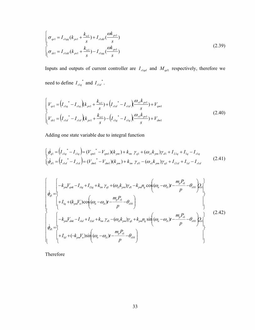
33
)()(
)()(
11
1111
11
1111
s
kI
s
kkI
s
kI
s
kkI
psqqs
ispsddsds
psdds
ispsqqsqs
(2.39)
Inputs and outputs of current controller are qdsI 1 and 1qdM respectively, therefore we
need to define *1qsI and *
1dsI .
111
1*
11
11*
11
111
1*
11
11*
11
)()(
)()(
dmpss
qsqsis
psdsdsds
qmpss
dsdsis
psqsqsqs
Vs
kII
s
kkIIV
Vs
kII
s
kkIIV
(2.40)
Adding one state variable due to integral function
dsddLqpmsdimpmdmdmdsdsd
qsqqLdpmsqimpmqmqmqsqsq
IIIkkkVVII
IIIkkkVVII
1111111*
11*
11
1111111*
11*
11
)())((
)())((
(2.41)
101
11
1101
1111111
1
101
11
1101
1111111
1
)(sin)(
)(sin)(
)(cos)(
)(cos)(
ssp
snnpmd
sssp
snqpmqpmsdimdLdsdmpm
d
ssp
snnpmq
sssp
snqpmdpmsqimqLqsqmpm
q
p
PmtVkI
Qp
PmtnkkkIIVk
p
PmtVkI
Qp
PmtnkkkIIVk
(2.42)
Therefore

34
)1
(
)1
(
1*
11
1*
11
pII
pII
dsdsd
qsqsq
(2.43)
11111111*
11
11111111*
11
)()(
)()(
dmqpssdispsdsdsds
qmdpssqispsqsqsqs
VkkkIIV
VkkkIIV
(2.44)
111111
11111111*
1
1
111111
11111111*
1
1
)(
)()())((
)(
)()())((
dmqpssdis
psdsddLqpmsdimpmdmdm
ds
qmdpssqis
psqsqqLdpmsqimpmqmqm
qs
Vkk
kIIIkkkVVV
Vkk
kIIIkkkVVV
(2.45)
with substituting (2.19) into (2.45)
111111
1
111
1111101
11
1
111111
1
111
1111101
11
1
)(
)()())()(sin)((
)(
)()())()(cos)((
dmqpssdis
ps
dsddL
qpmsdimpmdmssp
snsqn
ds
qmdpssqis
ps
qsqqL
dpmsqimpmqmssp
snsqn
qs
Vkk
k
III
kkkVs
PmtQnV
V
Vkk
k
III
kkkVs
PmtQnV
V
So the qd-axis output voltages of converter are

35
101
1111
1101
1111111
11111111111
1
101
1111
1101
11111
1111111111111
1
)(sin)(
)(sin)(
)()1(
)(cos)(
)(cos)(
)1(
ssp
snnpspmdps
sssp
snqpspmdisqpss
dpsimqpspmsdLpsdspsdmpspm
ds
ssp
snnpspmqps
sssp
snqpspmdpss
qisdpspmsqpsimqLpsqspsqmpspm
qs
s
PmtVkkIk
Qs
Pmtnkkkk
kkkkIkIkVkk
V
s
PmtVkkIk
Qs
Pmtnkkk
kkkkkIkIkVkk
V
(2.46)
And state space equations of the converter output currents
101
111111
1101
1111111
1111111111111
11
101
1111111
1101
1111111
111111111111
11
)(sin)(
)(sin)(
)()()(
1
)(cos)(
)(cos)(
)()(
1
ssp
snnpspmdpsdpsim
sssp
snqpspmdisqpss
qpspmsdLpsdsspsqsssdmpspm
sds
ssp
snnpspmqpsdpspms
sssp
snqpspmdpssqis
qpsimqLpsdsssqsspsqmpspm
sqs
s
PmtVkkIkkk
Qs
Pmtnkkkk
kkIkIRkILVkk
LpI
s
PmtVkkIkkk
Qs
Pmtnkkkk
kkIkILIRkVkk
LpI
(2.47)

36
0 500 1000 1500 2000 2500 3000 3500 400059.55
59.6
59.65
59.7
59.75
59.8
59.85
59.9
59.95
P1 (W)
fs1
(Hz)
Figure 2.3 Frequency of the system
2.4 Equilibrium Curves of One Converter System
In this section to draw the equilibrium curve of the one converter standalone
system and define steady state operation points without linearization, the
CL_MATCONT software package [110] along with MATLAB is used. Figure 2.3 shows
trend of frequency with change of active power of constant load. With increase of
constant load active power from zero to 4000W, droop control reduces frequency till
59.57Hz. Output active power of the converter increases to about 4800W to feed the
loads in Figure 2.4.

37
0 500 1000 1500 2000 2500 3000 3500 4000500
1000
1500
2000
2500
3000
3500
4000
4500
5000
P1 (W)
Ps1
(co
nver
ter
activ
e po
wer
) (W
)
Figure 2.4 Output active power of converter
0 500 1000 1500 2000 2500 3000 3500 400018
19
20
21
22
23
24
25
26
27
28
P1 (W)
Qs1
(co
nver
ter
reac
tive
pow
er)
(Var
)
Figure 2.5 Output reactive power of converter

38
0 500 1000 1500 2000 2500 3000 3500 40000.92
0.93
0.94
0.95
0.96
0.97
0.98
0.99
1
P1 (W)
M1
(con
vert
er m
odul
atio
n in
dex)
(V
dc1=
260
V)
Figure 2.6 Modulation index magnitude of converter
0 500 1000 1500 2000 2500 3000 3500 4000119.966
119.968
119.97
119.972
119.974
119.976
119.978
119.98
P1 (W)
Vm
1 (L
oad
volta
ge m
agni
tude
) (V
)
Figure 2.7 Load voltage magnitude

39
0 500 1000 1500 2000 2500 3000 3500 4000783
784
785
786
787
788
789
790
P1 (W)
PL1
(W
)
Figure 2.8 Active power of linear RL load
0 500 1000 1500 2000 2500 3000 3500 40001038
1038.2
1038.4
1038.6
1038.8
1039
1039.2
1039.4
1039.6
1039.8
P1 (W)
QL1
(V
ar)
Figure 2.9 Reactive power of linear RL load

40
modulation index magnitude of the converter in Figure 2.6 increases and is always less
than unity. Change of frequency affects the amount of intendance of transmission lines
and linear load so there is a small change in voltage magnitude and active power of linear
load that is related to it; in addition, reactive power of linear load has a small change in
reactive power. It should be noted that change of voltage and consequently active and
reactive of the linear load due to the change of constant load and frequency are small and
almost negligible.
2.5 Autonomous Operation of Two Converter System
To describe how droop control shares total load in a multi converter system, a two
converter system is represented in this part. The dynamic model of the system is
described as a general case of a multi converter system. Control units are designed in
separated qd-axis format with a phase locked loop (PLL) for each converter. The system
is simulated in MATLAB software.
Figure 2.10 represents a single line diagram of a two converter system. The whole
system is working autonomously. Microgrid consists of two DG units which have their
own local loads which are connected to each other. Three different types of loads are
used, a linear RL load, a constant load and a nonlinear load that is related to voltage
magnitude and frequency. A transmission line connects local loads to the converters. Its
resistance includes transmission line loss and converter switching loss. A capacitor is
added at the point of load connection to remove output noise and voltage fluctuations of

41
DC/ACConverterVdc1
Vm1Is1
Rs1 Ls1
Iin1
A1 Ai
LiR
LiL
LiI
iPdiC
iI
m
i=1,2
DC/ACConverterVdc2
Vm2
Is2Rs2 Ls2
Iin2
A2
I 12
iQ
1sP 1sQ
2sP 2sQ
1
2
1s
2s
iNonP
iNonQ
iNonI
R12
L12
Figure 2.10 Schematic diagram of study system
the converter and prepare a smooth load voltage. The input sources are assumed to have
enough capacity to feed the loads and both converters are sharing total load.
2.5.1 Dynamic Model
A droop control is applied to each converter to share total load based on local
measurement so each DG unit is considered with its own local frequency which is
measured using a phase lock loop (PLL). Dynamic equations of the system are as follows
(dt
dp and 2,1i )
2dci
isisisisimisi
VMIRpILVV (2.48)
where siV , siI , and iM are output phase voltage, phase current, and modulation index of
converters. miV , siR and siL are load voltage, transmission line resistance and inductance
of DGi respectively.
Linear loads equation

42
LiLiLiLimi pILIRV (2.49)
where LiI , LiR and LiL are phase current, resistance and inductance of linear load
respectively.
Transmission line between two converters equation
ijijmjmi pILIRVV 1212 (2.50)
Where 12R and 12L are resistance and inductance of connection line.
Capacitor voltage equations
iNoniLiijsimid IIIIIpVC 1 (2.51)
where iI , iNonI and diC are phase currents of constant load and nonlinear load and
capacitance of DGi.
Nonlinear load equations
220 )()(
n
si
n
miiiNon f
f
V
VPP (2.52)
220 )()(
n
si
n
miiiNon f
f
V
VQQ (2.53)
Where 0iP and 0iQ are initial active and reactive powers of nonlinear loads. miV and sif
are local load voltage magnitude and frequency. nV and nf are nominal voltage and
frequency of the system.
For each converter its own local frequency as synchronous reference frame is
used to transform dynamic equations of the system to qd reference frame and produce
time invariant variables.
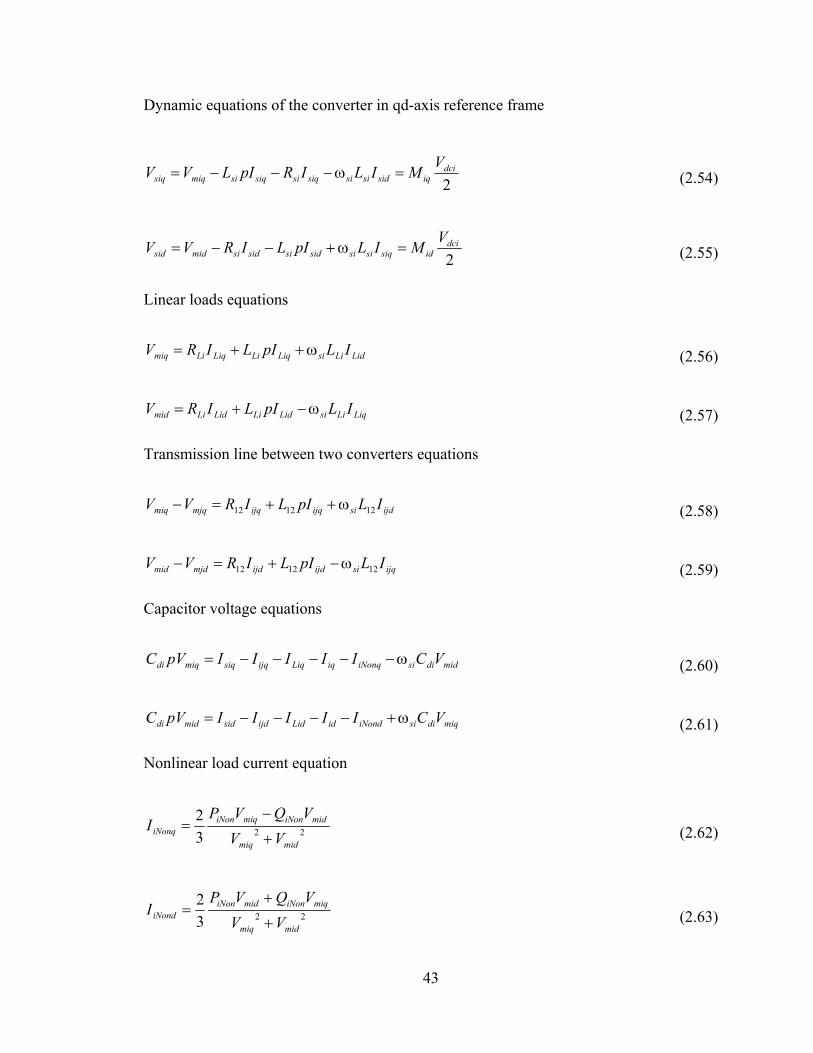
43
Dynamic equations of the converter in qd-axis reference frame
2dci
iqsidsisisiqsisiqsimiqsiq
VMILIRpILVV (2.54)
2dci
idsiqsisisidsisidsimidsid
VMILpILIRVV (2.55)
Linear loads equations
LidLisiLiqLiLiqLimiq ILpILIRV (2.56)
LiqLisiLidLiLidLimid ILpILIRV (2.57)
Transmission line between two converters equations
ijdsiijqijqmjqmiq ILpILIRVV 121212 (2.58)
ijqsiijdijdmjdmid ILpILIRVV 121212 (2.59)
Capacitor voltage equations
middisiiNonqiqLiqijqsiqmiqdi VCIIIIIpVC (2.60)
miqdisiiNondidLidijdsidmiddi VCIIIIIpVC (2.61)
Nonlinear load current equation
223
2
midmiq
midiNonmiqiNoniNonq
VV
VQVPI
(2.62)
223
2
midmiq
miqiNonmidiNoniNond
VV
VQVPI
(2.63)

44
siP siQ
si
Figure 2.11 Control unit diagram
Constant load current equation
223
2
midmiq
midimiqiiq
VV
VQVPI
(2.64)
223
2
midmiq
miqimidiid
VV
VQVPI
(2.65)
2.5.2 Controller Unit of Two Converter System
Since microgrid is works autonomously, voltage magnitude and frequency of each
DG unit should be defined along with the feed of the total load. This is illustrated in
Figure 2.11 the control unit of each converter consists of four main parts, a droop control
to share the load between converters, a voltage and an inner current control. A phase lock
loop (PLL) is added to align load voltage in q-axis reference frame and measure local
frequency.

45
2.5.3 Droop Control
Like one converter system, in a multi converter system
sipini Pm * (2.66)
siqinmi QnVV * (2.67)
where n and nV are rated frequency and rated voltage of the
In (2.68) and (2.69) the amount of droop coefficients are defined. The active
power droop coefficient is based on maximum change of frequency that is considered 1%
against maximum change of active power of converter which is nominal power of
converter.
maxsipi P
m
(2.68)
maxsiqi Q
Vn
(2.69)
For reactive power droop coefficient, the maximum tolerance of voltage is
considered 2%. It should be noted that to have the same frequency in the whole system
2211 spnspn PmPm (2.70)
Therefore
1
2
2
1
s
s
p
p
P
P
m
m (2.71)
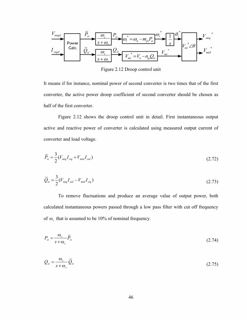
46
c
c
s
c
c
s
s
1
siqdI *midV
*miqV
*miV
miqdVsiP
~
siQ~
siP
siQ
*i
*i
*miV
sipini Pm *
siqinmi QnVV *
Figure 2.12 Droop control unit
It means if for instance, nominal power of second converter is two times that of the first
converter, the active power droop coefficient of second converter should be chosen as
half of the first converter.
Figure 2.12 shows the droop control unit in detail. First instantaneous output
active and reactive power of converter is calculated using measured output current of
converter and load voltage.
)(2
3~sidmidsiqmiqsi IVIVP (2.72)
)(2
3~siqmidsidmiqsi IVIVQ (2.73)
To remove fluctuations and produce an average value of output power, both
calculated instantaneous powers passed through a low pass filter with cut off frequency
of c that is assumed to be 10% of nominal frequency.
sic
csi P
sP
~
(2.74)
sic
csi Q
sQ
~
(2.75)

47
The outputs of droop control are voltage magnitude and angular frequency which
define the reference angle of the load voltage using an integrator. Thus qd axis reference
voltage can be determined as follows:
)cos( ***siimimiq VV (2.76)
)sin( ***siimimid VV (2.77)
where si is the reference angle for transformation to qd axis reference frame. This angle
is local frequency of each converter that is the output of PLL.
2.5.4 Voltage Control
To follow reference voltage, produced from droop control, a PI voltage controller
is designed. From Figure 2.13 and dynamic equation of the system in laplace format
middisiiNonqiqLiqijqsiqmiqdi VCIIIIIpVC (2.78)
miqdisiiNondidLidijdsidmiddi VCIIIIIpVC (2.79)
miqmiqmiqmiqmiqdi VVskpVC ))(( * (2.80)
midmidmidmidmiddi VVskpVC ))(( * (2.81)
where PI voltage controllers are
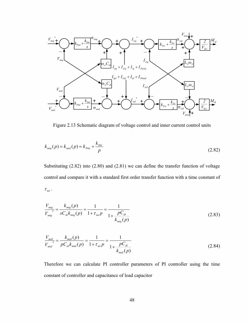
48
_
+ +
_
+
+
+
+++
_+ +
_+
++ +
_ _
*miqV
*midV
miqV
midV
s
kk iIm
Pmi miq
mids
kk iIm
Pmi
disiC
disiC
iNonqiqLiqijq IIII
iNondidLidijd IIII
sidI
siqI
*siqI
*sidI
s
kk Isi
Psi
s
kk Isi
Psi
sisiL
sisiL
siq
sid dciV
2
dciV
2 qiM
diM
+
+midV
miqV
Figure 2.13 Schematic diagram of voltage control and inner current control units
p
kkpkpk iIm
Pmimidmiq )()( (2.82)
Substituting (2.82) into (2.80) and (2.81) we can define the transfer function of voltage
control and compare it with a standard first order transfer function with a time constant of
mi .
)(1
1
1
1
)(
)(*
pk
pCppksC
pk
V
V
miq
dimimiqdi
miq
miq
miq
(2.83)
)(1
1
1
1
)(
)(*
pk
pCppkpC
pk
V
V
mid
dimimiddi
mid
mid
mid
(2.84)
Therefore we can calculate PI controller parameters of PI controller using the time
constant of controller and capacitance of load capacitor

49
p
kk
p
Cppkpk iIm
Pmimi
dimiqmiq
)()( (2.85)
mi
diPmi
Ck
and 0iImk (2.86)
For a fast voltage control response we need a small time constant but should still be much
larger than the switching time interval. It is chosen as ten times of switching time interval
swisi f
2
110 (2.87)
where swif is the switching frequency of converter of DGi.
Using the output of the voltage controller the reference output current of converter can be
defined as
middisiiNonqiqLiqijqmiqsiq VCIIIII * (2.88)
miqdisiiNondidLidijdmidsid VCIIIII * (2.89)
Where miq and mid are output voltage PI controller.
2.5.5 Current control
After controlling the load voltage magnitude and defining current reference, the
current controller will follow its reference. The advantage of inner current control is that
we can put a limiter in the reference current so we will apply an inherent current
protection to the system which is especially good for the power electronic converter
which has a limited rated capacity.

50
To design the inner current controller, using qd axis dynamic equations of the
system
sidsisimiqdci
qisiqsisiqsi ILVV
MIRpIL 2
(2.90)
siqsisidmidci
didssisidsi ILVV
MIRpIL 21 (2.91)
and
sidsidsidsiddssisidsi IIpkIRpIL ))(( *1 (2.92)
siqsiqsiqsiqsiqsisiqsi IIpkIRpIL ))(( * (2.93)
where PI current controller are
p
kkpkpk Isi
Psisidsiq )()( (2.94)
With substituting (2.94) into (2.92) and (2.93) we can define the transfer function of
current controller and compare it with a standard first order transfer function with a time
constant of si .
)(1
1
1
1
)(
)(*
pk
RpLppkRpL
pk
I
I
siq
sisisisiqsisi
siq
siq
siq
(2.95)
)(1
1
1
1
)(
)(*
pk
RpLppkRpL
pk
I
I
sid
sisisisidsisi
sid
sid
sid
(2.96)

51
Therefore we can calculate PI controller parameters of the current PI controller using the
time constant of the controller, and the resistance and inductance of the output
transmission line of converters
p
kk
p
RpLpkpk Isi
Psisi
sssiqsiq
11)()(
(2.97)
si
siPsi
Lk
and
si
siIsi
Rk
(2.98)
Because the current controller is the most inner control unit, it should be the fastest
controller. Its time constant is chosen as half of the voltage controller or five times the
switching frequency time intervals
swimi f
2
15 (2.99)
The modulation indices of the outputs of the controller will be
)(2
sidsisimiqsiqdci
qi ILVV
M (2.100)
)(2
siqsisimidsiddci
di ILVV
M (2.101)
52
si)(sKF s
1si
miaV
mibV
micV
mimiq VV )sin( siimimid VV
Figure 2.14 Block diagram of phase locked loop
2.5.6 Phase Lock Loop
To measure the frequency of the system and define a reference frequency for qd
transformation, a phase lock loop is designed and applied to each DG unit. Its dynamic is
added to the system equations to be more realistic. As it is shown in Figure 2.14 the three
phase PLL uses measured local load voltages and converts them to qd-axis frame then
compares d-axis voltage with zero as a reference. The error passes through a controller
and then through a low pass filter to remove noises. The idea of the PLL is to align
voltage to the q-axis and makes d-axis voltage zero, therefore
)sin( siimimid VV (2.102)
If 0midV 0)sin( sii isi
)sin(0 siimimid VVe (2.103)

53
If )( sii is very small we can assume
)()sin( siisii (2.104)
siF
siimi p
pKV
)()(
(2.105)
Therefore we can define the closed loop transfer function and compare it with second
order standard Butterworth filter
)(
)(
pKVp
pKV
Fmi
Fmi
i
si
(2.106)
211
2
211
2 2
2
nn
nn
IpllmiPpllmi
IpllmiPpllmi
i
si
ps
p
kVkpVp
kVkpV
(2.107)
mi
nPpll V
k 12 and
mi
nIpll V
k21
(2.108)
where is damping factor and is usually chosen as critical damping factor which is
707.0 and 1n is natural frequency which is chosen as )/(377 srad .
2.5.7 Simulation of Two Converter System
To verify the operation of the system and controllers, the autonomous system of
Figure 2.10 with two converters as DG units is simulated in MATLAB software. Table
2.1 shows the system parameters for simulation and the designed controller parameters

54
Table 2.1 System parameters of DG
nV 120V LiR 10 Ω
n 377(rad/s) LiL 0.0352H
siR 0.1Ω 10P 200W
siL 4e-3H 10Q 100Var
12R 0.04Ω c 37.7(rad/s)
12L 1e-3H swf 5KHz
diC 200e-6F dciV 300V
Table 2.2 Parameters of the designed controllers
Pmik 0.628 ikIm 0
Psik 25.13 Isik 628.32
Ppllk 4.44 Ipllk 1184
1pm 0.0038 2pm 0.0019
1qn 0.0012 2qn 0.0012
are shown in Table 2.2. To show the process of load sharing when DG units have
different nominal powers, the rated power of second converter is assumed to be two times
that of the first converter. As a result, the active droop coefficient of the second converter
is selected as half of that of the first converter. Figure 2.15 shows the reference of
constant load active and reactive power of the first and second converter. More over
Figure 2.16 illustrates output active and reactive power of converters and the process of
load sharing between two DG units. At 0.3s, 1.1s and 1.9s we have change of reference
active power and at 0.7s and at 5s reactive power references are changed. At 0.3s the first
constant load active power changes from 150W to 2000W. We can see that both active
powers of the converters change to feed the load. Output active power of DG1 changes
from 600W to 1250W and DG2 output active power, due to higher capacity and lower
active power coefficient, produces twice the previous power. Output active powers of
DG1 and DG2 also increase from 1250W and 2500W to 1900W and 3800W respectively
when the active power of second constant load rises to 2000W. In other regions active
power converter units are almost constant. Because we have the same frequency in the
whole system, both converters are sharing total active power based on their rated capacity

55
0.2 0.4 0.6 0.8 1 1.2 1.4 1.6 1.8 2 2.20
1000
2000
a) P
1
0.2 0.4 0.6 0.8 1 1.2 1.4 1.6 1.8 2 2.20
500
1000
b) Q
1
0.2 0.4 0.6 0.8 1 1.2 1.4 1.6 1.8 2 2.20
1000
2000
c) P
2
0.2 0.4 0.6 0.8 1 1.2 1.4 1.6 1.8 2 2.20
500
1000
d) Q
2
Time (sec)
0.2 0.4 0.6 0.8 1 1.2 1.4 1.6 1.8 2 2.20
500100015002000
a) P
s1
0.2 0.4 0.6 0.8 1 1.2 1.4 1.6 1.8 2 2.2-1000-500
0500
1000
b) Q
s1
0.2 0.4 0.6 0.8 1 1.2 1.4 1.6 1.8 2 2.20
1000200030004000
c) P
s2
0.2 0.4 0.6 0.8 1 1.2 1.4 1.6 1.8 2 2.2-1000-500
0500
d) Q
s2
Time (sec)
Figure 2.15 Active and reactive powers reference of first and second converters constant load, (a) and (b) are active and reactive powers of DG1 constant load, (c) and (d) are active and reactive powers of DG2 constant load.
Figure 2.16 Output active and reactive powers of first and second converters, (a) and (b) are active and reactive powers of DG1, (c) and (d) are active and reactive powers of DG2.
when either first or second local load active power changes. With change of first and
second load reactive powers, the output reactive powers of both converters are varied.
The sharing of reactive power is not exactly based on reactive power droop coefficient.
Because we can have different voltage magnitudes in different points of the power
system, reactive power change of each load more affects the output reactive power of its
local DG unit. Instead of some fluctuation, we can see small change in reactive power
with increase of active output power of the converters. Increase of active power droops
frequency so the reactive power of capacitor load capacitors and inductances changes and
causes the output reactive power of the converters to change in order to make the power
of total system balanced. Due to the small change of frequency, this effect on reactive
power is small.

56
0.2 0.4 0.6 0.8 1 1.2 1.4 1.6 1.8 2 2.2368
369
370
371
372
373
374
375
376
a) W
s1(r
ad/s
)
0.2 0.4 0.6 0.8 1 1.2 1.4 1.6 1.8 2 2.2368
369
370
371
372
373
374
375
376
b) W
s2(r
ad/s
)
Time (sec)
Figure 2.17 Actual local frequency (blue) and reference frequency (red) of the system, a) local frequency of DG1, b) local frequency of DG2
In Figure 2.17 the trend of measured local frequencies from the PLL and their
references from the output of the droop control and in different load conditions is
illustrated. Frequency of both converters reduces when the active power of the loads
increase. Different droop coefficient affects the output active power of converters base on
their rated power and both local frequencies are changing together so always total system
has the same frequency. Moreover control system follows the reference frequency fast so
the frequency ordered by droop control is always the same as the actual frequency of the
system. Change of reactive power doesn’t affect frequency.
Figure 2.18 shows qd-axis local load voltage of converters. Local frequency of
each converter is used for the qd reference frame transformation therefore both voltages
aligned with q-axis and d-axis voltages are almost zero. The voltage magnitude of both
converters changes with change of reactive power based on the droop control output.
With change of the second load reactive power the biggest effect is on the output reactive

57
power of DG2, and consequently on the voltage magnitude of second converter local
load. During the change of active power, voltage magnitudes are almost constant.
In Figure 2.19 modulation indices of the first and second converters are shown to
display the effects of the dynamics of the power system and control unit on the
converters. The sinusoidal pulse width modulation (SPWM) voltage source converters
are used to convert DC voltage to AC voltage. qd-axis modulation indices convert to abc
frame in the local synchronous frequency of each converter. Comparing modulation
indices with a triangular waveform of 5KHz switching frequency will produce switching
time intervals of each phase to convert DC input voltage to three phase AC output. qd-
axis modulation indices change with output active power of converters. With increase of
active power, the d-axis modulation indices’ magnitudes increase. The biggest effect of
0.2 0.4 0.6 0.8 1 1.2 1.4 1.6 1.8 2 2.2119
119.5120
120.5121
a) V
m1q
0.2 0.4 0.6 0.8 1 1.2 1.4 1.6 1.8 2 2.2-1
0
1
b) V
m1d
0.2 0.4 0.6 0.8 1 1.2 1.4 1.6 1.8 2 2.2119
119.5120
120.5121
c) V
m2q
0.2 0.4 0.6 0.8 1 1.2 1.4 1.6 1.8 2 2.2-1
0
1
d) V
m2d
Time (sec)
0.2 0.4 0.6 0.8 1 1.2 1.4 1.6 1.8 2 2.20.7
0.75
0.8
a) M
q1
0.2 0.4 0.6 0.8 1 1.2 1.4 1.6 1.8 2 2.2
-0.1
-0.05
b) M
d1
0.2 0.4 0.6 0.8 1 1.2 1.4 1.6 1.8 2 2.20.7
0.75
0.8
c) M
q2
0.2 0.4 0.6 0.8 1 1.2 1.4 1.6 1.8 2 2.2-0.25-0.2
-0.15-0.1
-0.05
d) M
d2
Time (sec)
Figure 2.18 Local load voltages, a) q-axis load voltage of DG1, b) d-axis load voltage of DG1, c) q-axis load voltage of DG2, d) d-axis load voltage of DG2.
Figure 2.19 Modulation indices of converters, a) q-axis modulation index of first converter, b) d-axis modulation index of first converter, c) q-axis modulation index of second converter, d) d-axis modulation index of second converter.

58
reactive power and voltage change is on q-axis modulation index. In the process of
changing loads, modulation indices’ magnitudes never saturate and they are always less
than unity.
2.6 Conclusion
In this chapter the dynamic model of a stand-alone single converter system is
presented. The droop control is applied to maintain voltage and frequency. Frequency
droops against output active power of converter and voltage magnitude droops against
reactive power. The PI load voltage control and inner current control are designed based
on the complex format of dynamic equations. Using bifurcation analysis, equilibrium
curves of one converter system are illustrated. Operation points of the controlled system
in different active power of constant load are shown.
The dynamic model of the two converter system as a multi-converter system is
explained as well as the droop control based on the rated capacity applied in order to
share total active and reactive power of the loads. Inner voltage and current controllers
based on separated qd-axis equations of the system are designed. The three phase PLL is
designed and added to each converter to measure instantaneous local frequency and
prepare the reference frequency for qd-axis transformation. The system is simulated in
MATLAB software. Simulation results show, based on rated capacity of each converter
and their droop coefficient, the active and reactive power of total load is shared between
them and change of frequency and voltage are related to active and reactive power
respectively.

59
CHAPTER 3
3.STEADY STATE ANALYSIS AND DYNAMIC CONTROL OF
PHOTOVOLTAIC SYSTEM
3.1 Introduction
Renewable energies are already playing important roles in the operation of
electric power systems. Most distributed generation (DG) units use renewable energies
such as solar (PV) and wind as their sources. Power electronic converters control the
output power and the voltage magnitude of the DG units.
In grid connected mode, the frequency and voltage magnitude of the load in the
Microgrid are adopted from the main grid. With control, it is possible to deliver the
maximum power of the sources to the grid or autonomous load. PV systems have a non-
linear output voltage and current relationship [111-112].
There are situations in which power systems with renewable energy sources are
normally operated in stand-alone modes. In such situations, there must be dedicated
power systems for rural areas, moveable military bases and facilities requiring premium
power quality. For the proper calculation and control operation of autonomous generation
systems, the dynamics of the power sources and the loads must be properly taken into
account through adequate system modeling. In autonomous mode, due to the power
balance between sources and loads, the PV system as the input source may not always
operate at the maximum power point. Under this condition of potential variation of PV

60
operating point, the control of the system should naturally consider the nonlinear
characteristics of the input source [113] in order to meet load requirements which could
be a combination of linear and non-linear loads. Alternatively, there should be another
source, like a battery, to maintain operation at the PV maximum power extraction
strategy. Under this condition, the steady state operation region of the system under
different loads, which define the currents, will be affected.
In this chapter, an autonomous (stand-alone) microgrid with a PV system as the
primary source is considered. In addition, a battery is connected to control DC link
voltage. The nonlinear characteristic of PV systems is added and the steady state
operation region of the system without linearization for different load conditions is
studied with MATLAB software.
3.2 Dynamic Model of the Stand-Alone System
Figure 3.1 shows a schematic diagram of the studied isolated power system. A PV
source and a battery are connected to the three phase DC/AC inverter. A boost DC/DC
converter increases the input PV voltage magnitude, and hence, controls the output power
of the source. A bidirectional DC/DC converter charges or discharges the battery to fix
DC link voltage. The inverter converts input DC voltage to AC and controls the voltage
magnitude of the load. A linear RL (resistance-inductance) load and a constant apparent
load are used. A capacitor is connected in parallel to the load to remove voltage
fluctuations. As shown, the structure of the battery consists of a constant dc source, and
internal capacitances and resistances.
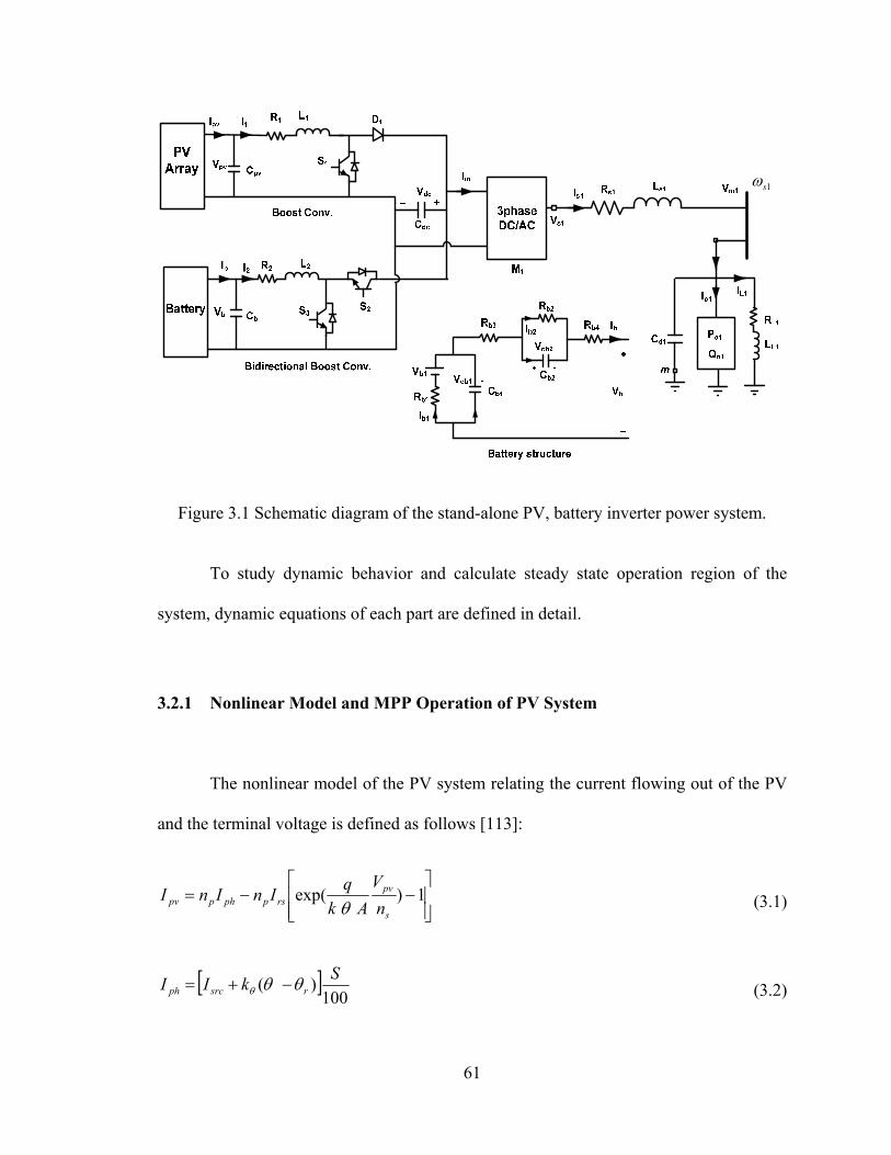
61
1s
Figure 3.1 Schematic diagram of the stand-alone PV, battery inverter power system.
To study dynamic behavior and calculate steady state operation region of the
system, dynamic equations of each part are defined in detail.
3.2.1 Nonlinear Model and MPP Operation of PV System
The nonlinear model of the PV system relating the current flowing out of the PV
and the terminal voltage is defined as follows [113]:
1)exp(
s
pvrspphppv n
V
Ak
qInInI
(3.1)
100
)(S
kII rsrcph (3.2)

62
Table 3.1 Parameters of PV system
rsI 72.1 e r k300
q Ce 19602.1 srcI A03.8
k KJe /38.1 23 k 0017.0
k298 sn 225
A 92.1 pn 250
S 1
In (3.1), rsI and are the reverse saturation current and the temperature of np
junction. srcI is the short-circuit current of one PV cell, sn and pn are the number of
series and parallel PV cells in a string, respectively. A is the ideality factor and S is
solar irradiation level. r is the cell reference temperature and k is the temperature
coefficient. )602.1( 19Ceq and )/38.1( 23 KJek are the unit electric charge and
Boltzmann’s constant. Table 3.1 shows parameters of PV system.
Figure 3.2 illustrates per unit output current and power of the PV system where
WPb 2000 and VVb 120 are selected as base values. At around puVpv 01.1 we have
maximum power point at unity irradiation level ( 1S ).
To define maximum power point in each solar irradiation level
1)exp(
s
pvrsppvphppvpv n
V
Ak
qInVInVP
(3.3)
1)exp(
100)(
s
pvrsppvrsrcppvpv n
V
Ak
qInV
SkInVP
(3.4)
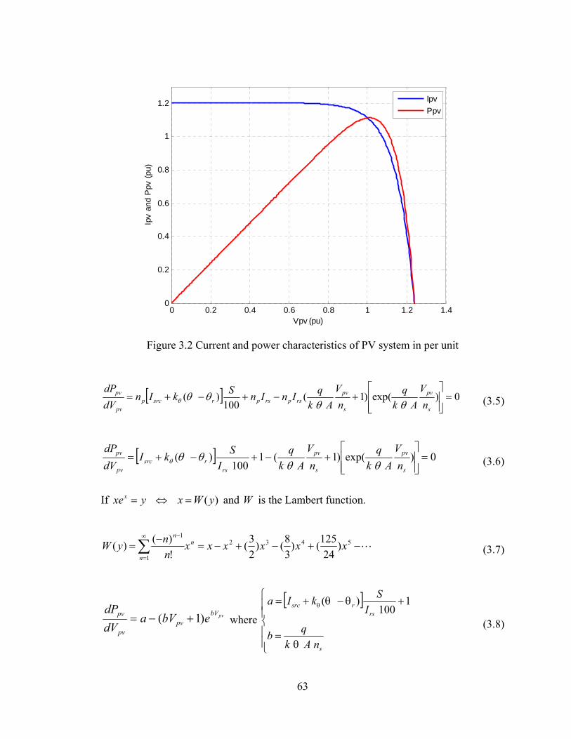
63
0 0.2 0.4 0.6 0.8 1 1.2 1.40
0.2
0.4
0.6
0.8
1
1.2
Vpv (pu)
Ipv
and
Ppv
(pu
)
Ipv
Ppv
Figure 3.2 Current and power characteristics of PV system in per unit
0)exp()1(100
)(
s
pv
s
pvrsprsprsrcp
pv
pv
n
V
Ak
q
n
V
Ak
qInIn
SkIn
dV
dP
(3.5)
0)exp()1(1100
)(
s
pv
s
pv
rsrsrc
pv
pv
n
V
Ak
q
n
V
Ak
q
I
SkI
dV
dP
(3.6)
If yxex )(yWx and W is the Lambert function.
5432
1
1
)24
125()
3
8()
2
3(
!
)()( xxxxxx
n
nyW n
n
n
(3.7)
pvbVpv
pv
pv ebVadV
dP)1( where
s
rsrsrc
nAk
qb
I
SkIa 1
100)(
(3.8)

64
0)1( pvbVpv
pv
pv ebVadV
dP (3.9)
aebV pvbVpv )1( (3.10)
1)1()1( eaebV pvbVpv (3.11)
)()1( 1eaWbVpv (3.12)
b
eaWV optpv
1)( 1 (3.13)
Figure 3.3 shows PV curve characteristics and calculated maximum power points
in 10 different irradiation levels from 0.01 to1. In Figure 3.4 trend of PV output voltage
at maximum power point (MPP) based on solar irradiation level is shown.
3.2.2 Boost Converter Connected to the PV System
The model of the PV, DC-DC converter is given as (dt
dp )
When 1S is ON ( 11 S )
1IIpVC pvpvpv (3.14)
1111 IRpILVpv (3.15)
When 1S is Off ( 11 D )
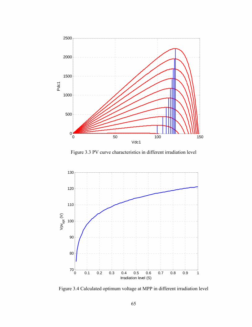
65
0 50 100 1500
500
1000
1500
2000
2500
Vdc1
Pdc
1
Figure 3.3 PV curve characteristics in different irradiation level
0 0.1 0.2 0.3 0.4 0.5 0.6 0.7 0.8 0.9 170
80
90
100
110
120
130
Irradiation level (S)
Vpv
opt (
V)
Figure 3.4 Calculated optimum voltage at MPP in different irradiation level

66
1IIpVC pvpvpv (3.16)
dcpv VIRpILV 1111 (3.17)
Therefore with combination of two modes ( 11 1 SD )
1IIpVC pvpvpv (3.18)
dcpv VSIRpILV )1( 11111 (3.19)
3.2.3 Bidirectional Boost Converter of Battery
In the bidirectional boost converter, when 2S is on ( 0,1 32 SS )
2IIpVC bbb (3.20)
dcb VVIRpIL 2222 (3.21)
When 2S is off ( 1,0 32 SS )
2IIpVC bbb (3.22)
bVIRpIL 2222 (3.23)
Therefore with combination of two modes ( 23 1 SS )
2IIpVC bbb (3.24)
dcb VSVIRpIL 22222 (3.25)

67
3.2.4 DC Link Equations
The dynamic equation of the DC link voltage
)(4
3)1()1( 111122112211 dsdqsqindcdc IMIMISISIISISpVC
(3.26)
3.2.5 Dynamic Model of the Battery
The model of the battery is expressed (Figure 3.1) as
222
111
4321
222
1111
0)(
0
0
cbbbb
cbbbb
bbbbcbcb
cbbb
cbbbb
pVCII
pVCII
VIRRVV
VIR
VVIR
(3.27)
bbbcbcbb
cbcbbbb
cbbcbbbb
IRRVVV
VpVCIR
VVpVCIR
)(
0)(
0)(
4321
2222
11111
(3.28)
bbbcbcbb
cbbbcbbb
cbbbbcbbb
IRRVVV
VIRpVCR
VVIRpVCR
)( 4321
22222
111111
(3.29)
3.2.6 Load Equation
The equations for the constant load currents expressed in the qd-axis synchronous
reference frame in terms of the constant real and imaginary powers are given as

68
21
21
11111 3
2
dmqm
dmoqmoqo
VV
VQVPI
(3.30)
21
21
11111 3
2
dmqm
qmodmodo
VV
VQVPI
(3.31)
Where 1oP and 1oQ are active and reactive power of the constant load.
3.2.7 Three Phase Converter Equations
The voltage source converter as illustrated in Figure 3.1 is modeled in the qd
reference frame below, where Mq1 and Md1 are the q and d modulation indices
)2
(1
)2
(1
1111111
11
1
1111111
11
1
qsssdssdmdc
ds
ds
dsssqssqmdc
qs
qs
ILIRVV
ML
pI
ILIRVV
ML
pI
(3.32)
3.2.8 Linear Load of DG1 (L1) Equations
The qd- synchronous reference frame equations of the resistance-inductance load
at the angular frequency ωs1 at the terminal of the voltage source inverter are given as
)(1
)(1
1111111
1
1111111
1
qLsLdLLdmL
dL
dLsLqLLqmL
qL
ILIRVL
pI
ILIRVL
pI
(3.33)

69
3.2.9 Capacitor of DG1 Equations
The qd equations of the load capacitors are given as
)(1
)(1
11101111
1
11101111
1
qmsdddLdsd
dm
dmsdqqLqsd
qm
VCIIIC
pV
VCIIIC
pV
(3.34)
3.3 Steady-State Operation
The steady state operation variables of the stand-alone power system operating at an
angular frequency of ωs1 are obtained when the derivatives of the states in the dynamic
equations in Section 3.2 are set equal to zero. The operation region is studied by changing
the active power of the constant load when Mq1=0.9, Md1=-0.16, Qo1 = 200Var, Vm1 =
120V, and the PV is providing maximum output power. Two different solar irradiations S
=1 and S = 0.7, and therefore two different PV system voltages Vpv = 121.25V and Vpv =
117.6V, are considered respectively. By increasing the load’s active power, the DC link
voltage in Figure 3.5 increases and the battery starts to discharge. In Figure 3.6, the
discharge of the battery reduces its output voltage. In Figure 3.7, the inverter’s output
active power increases gradually to meet the load requirement and ensure the power
balance. Due to the constant load voltage, active and reactive powers of the linear load
are constant. Thus with the constant reactive power of the other load, the total inverter
output reactive shown power in Figure 3.8, is constant.

70
0 500 1000 1500 2000 2500 3000406
408
410
412
414
416
418
420
422
424
P01 (W)
Vdc
(V
)
S=1
S=0.7
0 500 1000 1500 2000 2500 3000138.5
139
139.5
140
140.5
141
141.5
P01 (W)
Bat
tery
Vol
tage
(V
)
S=1
S=0.7
Figure 3.5 DC link voltage versus active power of constant load, blue(S = 1), red(S = 0.7)
Figure 3.6 Battery voltage versus active power of constant load, blue (S = 1), red(S = 0.7)
0 500 1000 1500 2000 2500 30000
500
1000
1500
2000
2500
3000
3500
P01 (W)
Ps1
(w
)
S=1
S=0.7
0 500 1000 1500 2000 2500 3000400.0117
400.0117
400.0117
400.0117
400.0117
400.0117
400.0117
400.0117
400.0117
400.0117
400.0117
P01 (W)
Qs1
(V
ar)
S=1
S=0.7
Figure 3.7 Inverter output active power versus active power of constant load, blue(S =1), red(S = 0.7)
Figure 3.8 Inverter output reactive power versus active power of constant load, blue(S=1), red(S = 0.7)
Figure 3.9 and Figure 3.10 illustrate the output current and power of the battery. When
total load is less than the maximum power supplied by the PV system, the excessive
power charges the battery. After approximately 1800W for unity irradiation level (S=1),
the total load exceeds the maximum power of PV system and the battery starts to
discharge, releasing power to the load. When the irradiation level of the PV system
decreases from 1 to 0.7, the maximum power decreases from 2229W to 1510W.
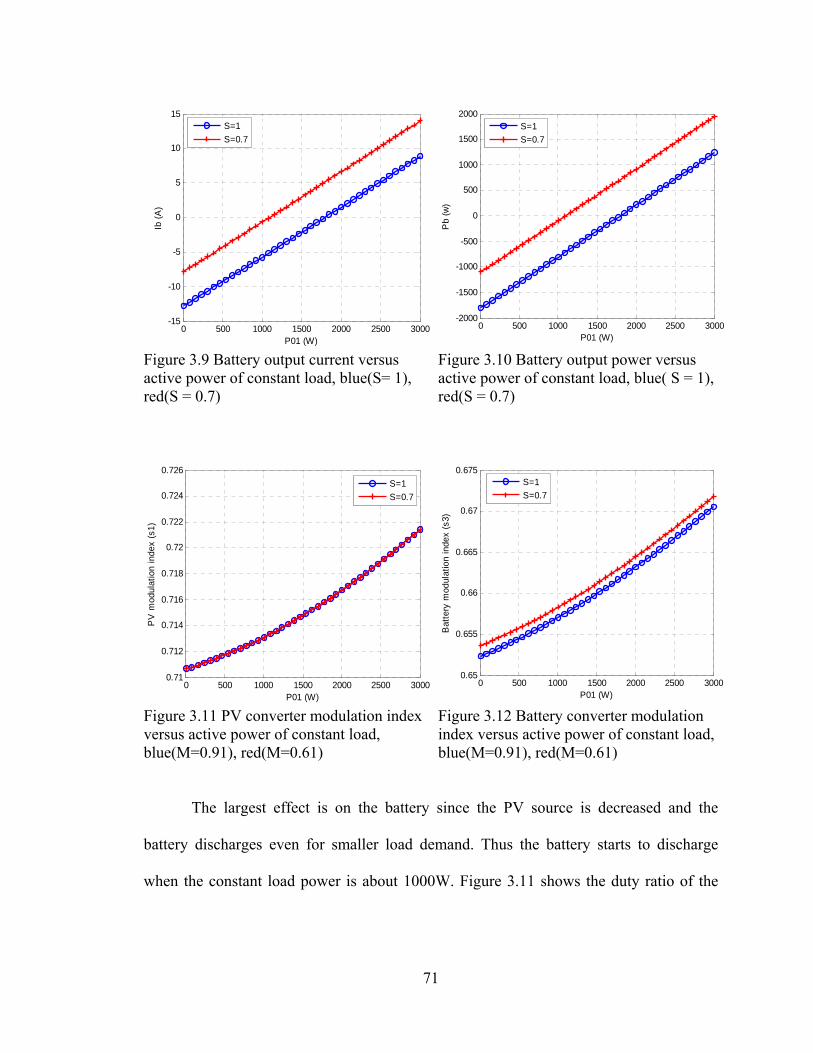
71
0 500 1000 1500 2000 2500 3000-15
-10
-5
0
5
10
15
P01 (W)
Ib (
A)
S=1
S=0.7
0 500 1000 1500 2000 2500 3000-2000
-1500
-1000
-500
0
500
1000
1500
2000
P01 (W)
Pb
(w)
S=1
S=0.7
Figure 3.9 Battery output current versus active power of constant load, blue(S= 1), red(S = 0.7)
Figure 3.10 Battery output power versus active power of constant load, blue( S = 1), red(S = 0.7)
0 500 1000 1500 2000 2500 30000.71
0.712
0.714
0.716
0.718
0.72
0.722
0.724
0.726
P01 (W)
PV
mod
ulat
ion
inde
x (s
1)
S=1
S=0.7
0 500 1000 1500 2000 2500 30000.65
0.655
0.66
0.665
0.67
0.675
P01 (W)
Bat
tery
mod
ulat
ion
inde
x (s
3)
S=1
S=0.7
Figure 3.11 PV converter modulation index versus active power of constant load, blue(M=0.91), red(M=0.61)
Figure 3.12 Battery converter modulation index versus active power of constant load, blue(M=0.91), red(M=0.61)
The largest effect is on the battery since the PV source is decreased and the
battery discharges even for smaller load demand. Thus the battery starts to discharge
when the constant load power is about 1000W. Figure 3.11 shows the duty ratio of the

72
DC-DC converter connected to the PV to meet the load demand. The battery converter’s
corresponding duty ratio is shown in Figure 3.12
3.4 Control Unit Design
3.4.1 Load Voltage Control
To follow the load reference voltage at rated value, a PI voltage controller is
designed. From Figure 3.13 and the dynamic equations of the system in Laplace format
given as
qmqmqmqmdmdsoqqLqsqmd VVskVCIIIpVC 11*
1111111111 ))(( (3.35)
dmdmdmdmqmdsoddLdsdmd VVskVCIIIpVC 11*
1111111111 ))(( (3.36)
where the PI voltage controllers are
s
kksksk Im
Pmdmqm1
111 )()( (3.37)
Substituting (3.37) into (3.35) and (3.36) we can define the transfer function of
voltage control and compare it with a standard first order transfer function with a time
constant of 1m as.
)(1
1
1
1
)(
)(
1
111
1*
1
1
sk
sCssksC
sk
V
V
qm
dmqmdi
qm
qm
qm
(3.38)

73
*1qmV
qmV 1
*1dmV
dmV 1
qm1
dm1s
kk Im
Pm1
1
qqL II 011
ddL II 011
11 ds C
*1qsI
s
kk Im
Pm1
1
11 ds C qsI 1
*1dsI
dsI 1
qs1
ds1s
kk Is
Ps1
1
11 ssL
1
2
dcV
1qM
1dM
1
2
dcV
dmV 1
qmV 1
s
kk Is
Ps1
1
11 ssL
Figure 3.13 Block diagram of DC-AC three phase converter control part
)(1
1
1
1
)(
)(
1
111
1*
1
1
sk
sCssksC
sk
V
V
dm
dmdmdi
dm
dm
dm
(3.39)
Therefore the PI controller parameters can be calculated using the time constant
of the controller and capacitance of the load capacitor as
s
kk
s
Cssksk Im
Pmm
dqmqm
11
1
111 )()(
(3.40)
1
11
m
dPm
Ck
and, 01Im k (3.41)
For a fast voltage control response, a small time constant is needed. It shouldn’t
be very small, but must be bigger than the switching time interval. It is therefore chosen
to be about ten times the switching time interval
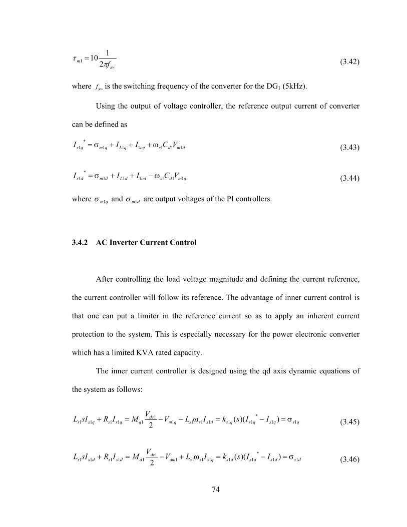
74
swm f
2
1101 (3.42)
where swf is the switching frequency of the converter for the DG1 (5kHz).
Using the output of voltage controller, the reference output current of converter
can be defined as
dmdsoqqLqmqs VCIII 111111*
1 (3.43)
qmdsoddLdmds VCIII 111111*
1 (3.44)
where qm1 and dm1 are output voltages of the PI controllers.
3.4.2 AC Inverter Current Control
After controlling the load voltage magnitude and defining the current reference,
the current controller will follow its reference. The advantage of inner current control is
that one can put a limiter in the reference current so as to apply an inherent current
protection to the system. This is especially necessary for the power electronic converter
which has a limited KVA rated capacity.
The inner current controller is designed using the qd axis dynamic equations of
the system as follows:
qsqsqsqsdsssqmdc
qqssqss IIskILVV
MIRsIL 11*
1111111
11111 ))((2
(3.45)
dsdsdsdsqsssdmdc
ddssdss IIskILVV
MIRsIL 11*
1111111
11111 ))((2
(3.46)

75
where the PI current controller is given by
s
kksksk Is
Psdsqs1
111 )()( (3.47)
Substituting (3.47) into (3.45) and (3.46), one can define the transfer function of
the current controller and compare it with a standard first order transfer function with a
time constant of 1s as follows:
)(1
1
1
1
)(
)(
1
111111
1*
1
1
sk
RsLsskRsL
sk
I
I
qs
sssqsss
qs
qs
qs
(3.48)
)(1
1
1
1
)(
)(
1
111111
1*
1
1
sk
RsLsskRsL
sk
I
I
ds
sssdsss
ds
ds
ds
(3.49)
Therefore the PI controller parameters of the current controller can be calculated
using the time constant of the controller, the resistance, and the inductance of the output
transmission line of converters
s
kk
s
RsLsksk Is
Pss
ssqsqs
11
1
1111 )()(
(3.50)
1
11
s
sPs
Lk
and
1
11
s
sIs
Rk
(3.51)
Being the inner most control unit, the current controller must have fastest
response. Therefore, its time constant is chosen to be half of the voltage controller or five
times the switching period

76
s
kk Ipvv
Ppvv*
pvV
pvV
pvv
pvI
s
kk Ipvi
Ppvi
*1I
1I
pvi
pvdc VV
dcV
1 1
~S
Co
mpa
rato
r
1S
Figure 3.14 Block diagram of PV DC-DC boost converter control part
swsi f
2
15 (3.52)
The modulation indices which are the outputs of the controllers will be
)(2
111111
1 dsssqmqsdc
q ILVV
M (3.53)
)(2
111111
1 qsssdmdsdc
d ILVV
M (3.54)
3.4.3 PV Voltage Control
As illustrated in Figure 3.14, the objective of the PV control is to follow
maximum power point. The output voltage controller is therefore designed using (3.18)
as
pvvpvpvpvvpvpvpv VVskIIsVC ))(( *1 (3.55)
where PV voltage reference ( *pvV ) comes from maximum power point tracking (MPPT).

77
)(
)(* sksC
sk
V
V
pvvpv
pvv
pv
pv and s
kksk Ipvv
Ppvvpvv )( (3.56)
IpvvPpvvpv
IpvvPpvv
pv
pv
kskCs
ksk
V
V
2* (3.57)
Comparing denominator of transfer function with denominator of second order
Butterworth filter
222 2 nnIpvvPpvvpv sskskCs (3.58)
The coefficients of outer voltage PI controller and the reference current for the inner
controller are defined as
pvnIpvv
pvnPpvv
Ck
Ck2
2 (3.59)
pvvpvII *1 (3.60)
The controller parameters are chosen as 7.0 and swdcn f 2.01 , where swdcf is the
switching frequency of the DC-DC converter which is chosen to be 5kHz for both DC–
DC converters.
3.4.4 PV Converter Current Control
To follow the reference current of the PV, based on the dynamic equation of the
converter interface inductor in (3.19)

78
pvipvidcpv IIskVSVIRsIL ))(()~
1( 1*
111111 (3.61)
where 1
~S is the average duty ratio of the converter.
)(
)(
11*
1
1
skRsL
sk
I
I
pvi
pvi
and
s
kksk Ipvi
Ppvipvi )( (3.62)
IpviPpvi
IpviPpvi
kskRLs
ksk
I
I
)( 11
2*1
1 (3.63)
2211
2 2)( nnIpviPpvi sskskRLs
12
112
Lk
RLk
nIpvi
nPpvi (3.64)
dc
pvipv
V
VS
1
~1 (3.65)
For faster inner current controller swdcn f 4.02 .
3.4.5 DC Link Voltage Control
The battery DC-DC converter should control the DC link voltage. Figure 3.15 and
Table 3.3 show the block diagram of battery converter control unit and battery
parameters. From the dynamics of the DC link voltage in (3.26) if the aforementioned
method is used
dcdcdcdcdsdqsqdcdc VVskIMIMISISsVC ))(()(4
3~)
~1( *
11112211 (3.66)
79
dcV
1*
dcV
dcV
s
kk Idc
Pdc dc
111111 )~
1()(4
3ISIMIM dsdqsq
2
~S
*2I
2I
bi
s
kk Ibi
Pbi
bV
2
~1
S
3S
2S
Figure 3.15 Block diagram of Battery DC-DC converter control part
)(
)(* sksC
sk
V
V
dcdc
dc
dc
dc
and
s
kksk Idc
Pdcdc )( (3.67)
IdcPdcdc
IdcPdc
dc
dc
kskCs
ksk
V
V
2*
(3.68)
222 2 nnIdcPdcdc sskskCs
dcnIdc
dcnPdc
Ck
Ck2
2 (3.69)
2
111111*
2 ~)
~1()(
4
3
S
ISIMIMI
dsdqsqdc (3.70)
3.4.6 Current Control of Battery Converter
The utilization of the battery inner current loop controller in addition to fault
protection, can limit the charge and the discharge current of the battery which is a key
factor in the determination of the battery life time. From (3.25)
bibidcb IIskVSVIRsIL ))((~
2*
222222 (3.71)

80
)(
)(
22*
2
2
skRsL
sk
I
I
bi
bi
and
s
kksk Ibi
Pbibi )( (3.72)
IbiPbi
IbiPbi
kskRLs
ksk
I
I
)( 22
2*2
2 (3.73)
2222
2 2)( nnIbiPbi sskskRLs
22
222
Lk
LLk
nIbi
nPbi (3.74)
dc
bib
V
VS
2
~ (3.75)
3.4.7 Voltage Control of PV in Disabled Battery
If the battery is disabled, DC link voltage should be regulated by PV converter.
To follow the reference voltage of the PV ( *pvV ) system that comes from MPPT
pvvpvpvpvvpvpvpv VVskIIsVC ))(( *1 (3.76)
IpvvPpvvpv
IpvvPpvv
pvvpv
pvv
pv
pv
kskCs
ksk
sksC
sk
V
V
2* )(
)( (3.77)
pvnIpvv
pvnPpvv
Ck
Ck2
2 (3.78)
pvvpvII *1 (3.79)

81
s
kk Ipvv
Ppvv*
pvV
pvV
pvv
pvI
s
kk Ipvi
Ppvi
*1I
1I
pvi1
~S
Co
mp
arat
or
1S
pvV
*dcV
dcV
s
kk Idc
Pdc dc
1
~1
1
S
)(4
311111 dsdqsq IMIMI
1
1
I
Figure 3.16 Block diagram of PV DC-DC boost converter control part if battery converter is disabled
3.4.8 PV Converter Current Control in Disabled Battery
In disabled battery mode, the dynamic equation of the PV current and therefore its
controller structure is changed as
pvipvidcpv IIskVSVIRsIL ))(()~
1( 1*
111111 (3.80)
The transfer function for current controller is
IpviPpvi
IpviPpvi
pvi
pvi
kskRLs
ksk
skRsL
sk
I
I
)()(
)(
112
11*
1
1 (3.81)
12
112
Lk
RLk
nIpvi
nPpvi
(3.82)
1
*~
1 S
VV pvipv
dc
(3.83)

82
c
c
s
c
c
s
s
1
qdsI 1*
1dmV
*1qmV
*1mV
qdmV 1 1
~sP
1
~sQ
1sP
1sQ
*1
*1
*1mV
)( *11
*1 QQnVV sqnm
)( *11
*1 PPm spn
Figure 3.17 Droop control unit
3.4.9 DC Link Voltage Control in Disabled Battery
To control the DC-link voltage
dcdcdcdcdsdqsqdcdc VVskIMIMISsVC ))(()(4
3)
~1( *
111111 (3.84)
IdcPdcdc
IdcPdc
dcdc
dc
dc
dc
kskCs
ksk
sksC
sk
V
V
2* )(
)( (3.85)
dcnIdc
dcnPdc
Ck
Ck2
2 (3.86)
1
11111
1
)(4
3~
I
IMIMIS
dsdqsqdc (3.87)
3.4.10 Droop Control
To guarantee total power balance either if total power of converter and battery is
less than total load or total load is less than produced power, a droop control is used.
83
The droop control droops frequency and voltage against output active and reactive
power of the three phase converter respectively.
)( *11
*1 PPm spn (3.88)
)( *11
*1 QQnVV sqnm
(3.89)
where n and nV are rated frequency and rated voltage of the system. 1pm , 1qn , 1sP and
1sQ are active power droop coefficients, reactive power droop coefficient, output active
power and output reactive power of converter, respectively. *P and *Q are desired
active and reactive powers of the converter. In this case *P is maximum power of PV
system that comes from MPPT and *Q is considered zero.
In (3.90) and (3.91) the amount of droop coefficients are defined. The active
power droop coefficient and reactive power droop coefficient are based on maximum
change of frequency and voltage respectively.
max11
sp P
m
(3.90)
max11
sq Q
Vn
(3.91)
Figure 3.17 shows the droop control unit in detail. First the instantaneous output
active and reactive powers of the converter are calculated using measured output current
of the converter and load voltage.
)(2
3~11111 dsdmqsqms IVIVP (3.92)

84
)(2
3~11111 qsdmdsqms IVIVQ (3.93)
To remove fluctuations and produce average values of output powers, both
calculated instantaneous powers are passed through a low pass filter with a cut off
frequency of c .
11
~s
c
cs P
sP
(3.94)
11
~s
c
cs Q
sQ
(3.95)
The outputs of droop control are voltage magnitude and angular frequency which
define the reference angle of the load voltage using an integrator. Thus the qd-axis
reference voltage can be determined as follows:
)cos( 1*
1*
1*
1 smqm VV (3.96)
)sin( 1*
1*
1*
1 smdm VV (3.97)
3.4.11 Phase Locked Loop
To measure the frequency of the system and define reference frequency for qd
transformation a phase lock loop (PLL) is designed and applied to each DG unit.
)sin( 1111 smdm VV (3.98)
If 01 dmV 0)sin( 11 s 11 s
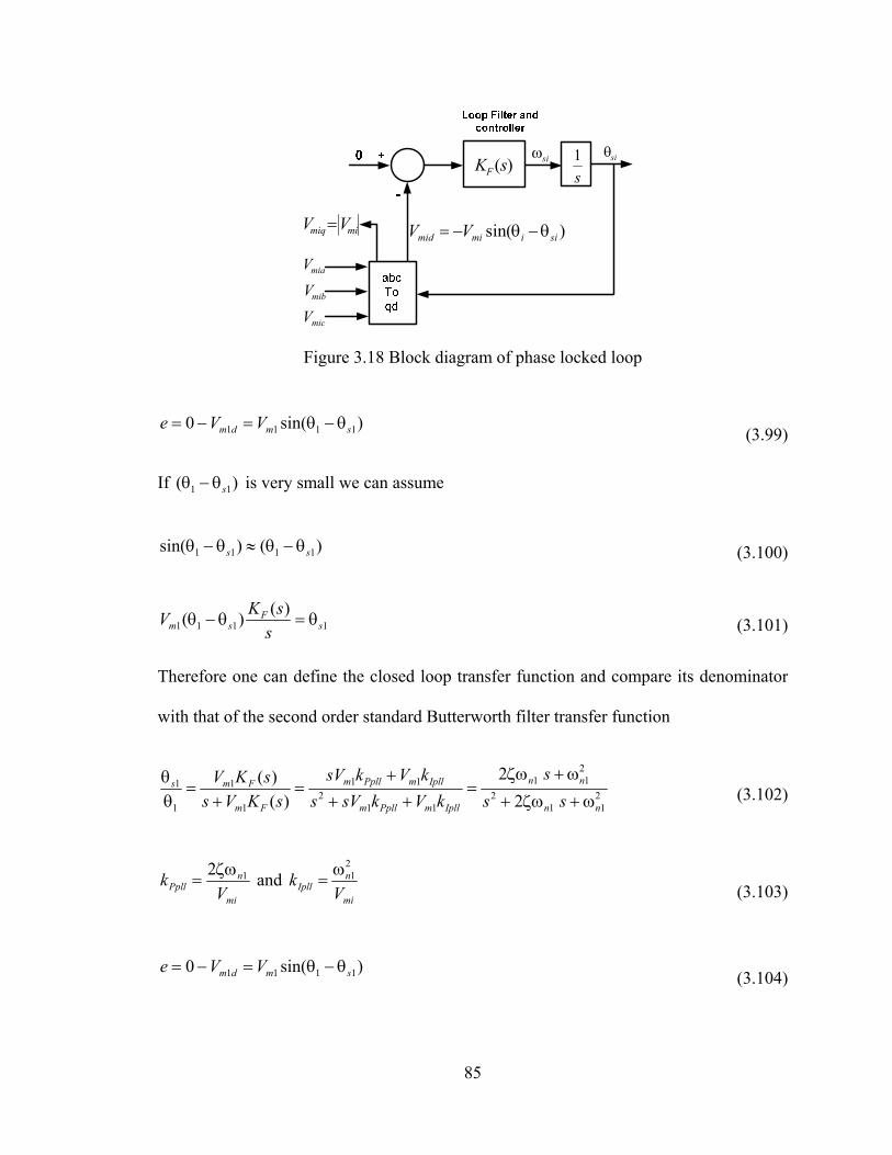
85
si)(sKF s
1si
miaV
mibV
micV
mimiq VV )sin( siimimid VV
Figure 3.18 Block diagram of phase locked loop
)sin(0 1111 smdm VVe (3.99)
If )( 11 s is very small we can assume
)()sin( 1111 ss (3.100)
1111
)()( s
Fsm s
sKV (3.101)
Therefore one can define the closed loop transfer function and compare its denominator
with that of the second order standard Butterworth filter transfer function
211
2
211
112
11
1
1
1
1
2
2
)(
)(
nn
nn
IpllmPpllm
IpllmPpllm
Fm
Fms
ss
s
kVksVs
kVksV
sKVs
sKV
(3.102)
mi
nPpll V
k 12 and
mi
nIpll V
k21
(3.103)
)sin(0 1111 smdm VVe (3.104)

86
Table 3.2 Parameters of power system
1sR 1.0 1R 2.0
1sL He 34 1L He 32
1LR 10 pvC Fe 6100
1LL H0352.0 2R 2.0
1dC Fe 6200 2L He 32
dcC Fe 35 bC Fe 6100
Table 3.3 Parameters of the battery
1bR 05.0 bV V48
1bC F54000 3bR 002.0
2bR 001.0 4bR 05.0
2bC F1
Table 3.4 PI controllers’ coefficients
1Pmk 377.0 1Imk 0
1Psk 13.25 1Isk 32.628
Ppvvk 053.0 Ipvvk 21.14
Ppvik 866.0 Ipvik 26.284
Pdck 66.2 Idck 6.710
Pbik 866.0 Ibik 26.284
Ppllk 44.4 Ipllk 1184
1pm 438 e 1qn 412 e
)sin(0 1111 smdm VVe (3.105)
where is damping factor and is usually chosen as critical damping factor which is
707.0 .
3.5 Simulation Results
To show the performance of the designed controllers, the studied system is simulated in
MATLAB software. Table 3.2 gives the parameters of the system in Figure 3.1.

87
0.2 0.3 0.4 0.5 0.6 0.7 0.8 0.9 11000
1200
1400
1600
1800
2000
2200
2400
2600
2800
3000
P1
and
Ps1
(W
)
Time(sec)
Ps1
P1
0.2 0.3 0.4 0.5 0.6 0.7 0.8 0.9 10.13
0.14
0.15
0.16
0.17
0.18
0.19
0.2
0.21
0.22
Bat
tery
Mod
ulla
tion
(s2)
Time(sec)
Figure 3.19 Constant load and inverter output active powers
Figure 3.20 Battery converter modulation index
0.2 0.3 0.4 0.5 0.6 0.7 0.8 0.9 1-15
-10
-5
0
5
10
15
20
I2 (
A)
Time(sec)0.2 0.3 0.4 0.5 0.6 0.7 0.8 0.9 1
298
298.5
299
299.5
300
300.5
301
301.5
302
302.5
303
Vdc
(V
)
Time(sec)
Figure 3.21 Battery output current Figure 3.22 DC link voltage
Parameters of the battery and PI controllers’ coefficients are presented in Table 3.3 and
Table 3.4 respectively. The PV system is always working in maximum power point and
the battery converter tries to control DC link voltage and limit maximum charge or
discharge currents of the battery that are chosen 300V and 20A respectively. Figure 3.19
shows the constant active load power changes at 0.3s and 0.7s from the lower to the
higher than rated power of PV system (2300W at unity irradiation level) with constant
reactive load power of 20Var. With a change of constant load active power, the output
active power of the inverter changes to feed both the linear and the constant loads.
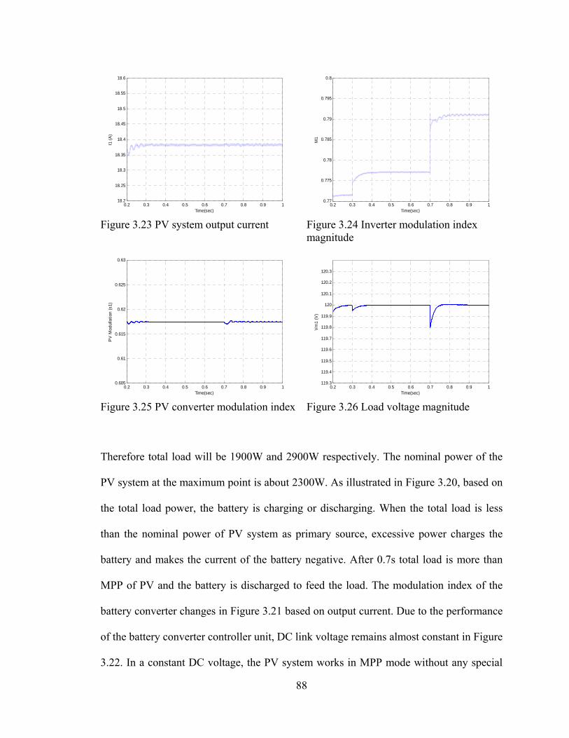
88
0.2 0.3 0.4 0.5 0.6 0.7 0.8 0.9 118.2
18.25
18.3
18.35
18.4
18.45
18.5
18.55
18.6
I1 (
A)
Time(sec)0.2 0.3 0.4 0.5 0.6 0.7 0.8 0.9 1
0.77
0.775
0.78
0.785
0.79
0.795
0.8
M1
Time(sec)
Figure 3.23 PV system output current Figure 3.24 Inverter modulation index magnitude
0.2 0.3 0.4 0.5 0.6 0.7 0.8 0.9 10.605
0.61
0.615
0.62
0.625
0.63
PV
Mod
ulla
tion
(s1)
Time(sec)0.2 0.3 0.4 0.5 0.6 0.7 0.8 0.9 1
119.3
119.4
119.5
119.6
119.7
119.8
119.9
120
120.1
120.2
120.3
Vm
1 (V
)
Time(sec)
Figure 3.25 PV converter modulation index Figure 3.26 Load voltage magnitude
Therefore total load will be 1900W and 2900W respectively. The nominal power of the
PV system at the maximum point is about 2300W. As illustrated in Figure 3.20, based on
the total load power, the battery is charging or discharging. When the total load is less
than the nominal power of PV system as primary source, excessive power charges the
battery and makes the current of the battery negative. After 0.7s total load is more than
MPP of PV and the battery is discharged to feed the load. The modulation index of the
battery converter changes in Figure 3.21 based on output current. Due to the performance
of the battery converter controller unit, DC link voltage remains almost constant in Figure
3.22. In a constant DC voltage, the PV system works in MPP mode without any special

89
change in its output current and modulation index as shown in Figure 3.23 and Figure
3.24 respectively. With increase of the load active power, modulation index of the three
phase inverter increases in Figure 3.25 and is always less than unity. In Figure 3.26, load
voltage magnitude experiences a small voltage sag in the instant of load change but it
reaches nominal value and remains constant for less than 50ms using a three phase
inverter controller.
To show the effect of array shading, the irradiation level at 0.5s is changed from
unity to 0.7, when the total load is kept constant at 2000W. Based on the proven equation
of optimum PV voltage, to follow maximum power point, the reference PV voltage
changes from 121.25V to 117.6V and the corresponding maximum output power of the
PV changes from 2300W to 1500W. Figure 3.27b shows that the PV controller follows
the reference voltage perfectly to produce maximum possible active power. Because the
total load is more than the maximum power of the PV system, the battery will discharge.
In Figure 3.27, with decrease of output PV current due to irradiation level reduction, the
battery produces positive current to meet the load requirement and keep the DC link
voltage constant.
3.6 Conclusions
In this chapter, the model and steady state performance characteristics of an autonomous
power system fed by a PV source and battery are set forth. The nonlinearities of the PV
and load are included in the model. At steady-state, when the PV system is working at the
maximum power point, it is observed that with an increase of the load, the dc link voltage

90
0.6 0.65 0.7 0.75 0.8 0.85 0.9 0.95 1
0.8
1
a)Ir
radi
atio
n Le
vel
Time(sec)
0.6 0.65 0.7 0.75 0.8 0.85 0.9 0.95 1115
120
125
b)V
pv-r
ef a
nd V
pv
Time(sec)
Vpv-ref (V)
Vpv (V)
0.6 0.65 0.7 0.75 0.8 0.85 0.9 0.95 110
15
20
c)Ip
v (A
)
Time(sec)
0.6 0.65 0.7 0.75 0.8 0.85 0.9 0.95 1-10
0
10
20
d)Ib
(A
)
Time(sec)
0.6 0.65 0.7 0.75 0.8 0.85 0.9 0.95 1295
300
305
e)V
dc (
V)
Time(sec)
Figure 3.27 Operation under different irradiation level. (a) irradiation level, (b) reference and actual PV voltage, (c) PV output current, (d) battery output current, (e) Dc link
voltage
increases to meet the constant load voltage when the voltage source converter operates at
a constant modulation index. The battery discharges when total load is more than
maximum power of the PV system. Under a lower irradiation level, the maximum power
of PV system decreases, thus the battery discharges even under reduced load demand.
With reduction of the inverter modulation index magnitude, to meet constant load

91
voltage, the input DC link voltage and the duty ratios of the two boost converters
interfacing the sources are increased.
Controller parts of DC/AC inverter and DC/DC converters are designed. The
objectives of the inverter and battery converter are to control load voltage and DC link
voltage respectively. PV converter tries to operate in maximum power point. If load
power is more than the maximum power of PV system and the battery is discharged,
droop control manages frequency and load voltage to guarantee total load balance. The
three phase inverter controls the frequency and voltage magnitude of the load. Simulation
results prove that with the change of load or irradiation level, controllers enable following
of the reference and meet load requirements in standalone mode condition.

92
CHAPTER 4
4.STEADY STATE ANALYSIS AND DYNAMIC CONTROL OF PV
SYSTEM CONNECTED TO THE MAIN GRID
4.1 Introduction
The goal for the microgrid with renewable energy sources is to transfer the
maximum possible power in grid connected mode. Since the voltage magnitude and
frequency are adapted from the main grid, the controller objectives are different in this
mode than in autonomous mode operation.
In grid connected mode the output active and reactive power or input DC–link
voltage magnitude can be controlled. In this chapter, a controller for grid connected
operation of a microgrid with a photovoltaic (PV) system as an input source has been
designed.
In the first section a single converter as a DG unit connected to a local linear RL
and a non-linear voltage dependent load along with a capacitor to remove harmonics and
stabilize load voltage is considered. The system equations are transformed from abc to
qdo in synchronous reference frame and dynamic equations are defined.
Two different control algorithms are considered. First the objective is to control input DC
voltage and assume load voltage is constant because it is connected to the main grid.
Secondly, with assumption of constant input DC voltage source, the load voltage is
controlled. In both algorithms we have an inner current control loop which controls qd-
axis output current of the converter separately.

93
LiR
LiL
aLii
iPdiC
aii
iQ
1sP 1sQ
Figure 4.1 Schematic diagram of a DG system with PV source connected to the grid
After designing controllers, a state space model of the whole system is defined
and bifurcation analysis is applied to the system to find equilibrium curves of parameters
and bifurcation points in the operation region. The simulation results prove the
performance of the designed controllers.
4.2 Dynamic Model of the System
Figure 4.1 shows the block diagram of a grid connected distributed generation
(DG) system. A voltage source converter converts DC input to AC output voltage. A
linear RL load and a constant load are connected to the converter through a transmission
line. A capacitor is connected to remove the high frequency voltage harmonics out of the
three phase inverter and smooth the load voltage. Another transmission line connects the
system to the main network with constant voltage magnitude and frequency.
The dynamic equations of the system in three phase abc frame are as follows:

94
The inverter transmission line dynamic equations
csscsscmas
bssbssbmas
assassamas
IRpILVV
IRpILVV
IRpILVV
111111
111111
111111
(4.1)
The three phase inverter equations
)12(2
)12(2
)12(2
11
11
11
bpdc
noas
bpdc
noas
apdc
noas
sV
VV
sV
VV
sV
VV
(4.2)
where abcsV 1 , abcsI 1 and abcps are output phase voltages, phase currents and switching
functions of DG1 (VSC1).
Linear Load of DG1 (L1) equations
cLLcLLcm
bLLbLLbm
aLLaLLam
pILIRV
pILIRV
pILIRV
11111
11111
11111
(4.3)
where abcLI 1 are phase currents of linear load (L1) of DG1
The main grid equations
scsscscmsc
sbssbsbmsb
sassasamsa
IRpILVV
IRpILVV
IRpILVV
1
1
1
(4.4)
Capacitor of DG1 Equations

95
ccLsccscmd
bbLsbbsbmd
aaLsaasamd
IIIIpVC
IIIIpVC
IIIIpVC
11111
11111
11111
(4.5)
where abcI1 are the phase currents of second (nonlinear) load of DG1.
The input DC current of DG1
)( 111111 cpcsbpbsapaspvinpvdc sIsIsIIIIpVC (4.6)
where abcs are modulation signals of three phase inverter. qd-axis dynamic equations of
the system in grid frequency synchronous reference frame are as follows:
)()(sin
)()(cos
10101111
10101111
ssd
ssq
tMM
tMM
(4.7)
where 1 and 10 are frequency and initial angle of converter and 1s and 10s are
instantaneous frequency and initial angle of the system that is measured by a phase
locked loop (PLL). 1M , 1qM and 1dM are modulation index magnitude, q-axis
modulation index and d axis modulation index of the converter respectively.
Load voltage equations
0
)()(cos
1
110101111
dm
mssssmqm
V
VtVV (4.8)
where 1mV is the load voltage magnitude.
)2
(1
)2
(1
1111111
11
1
1111111
11
1
qsssdssdmdc
ds
ds
dsssqssqmdc
qs
qs
ILIRVV
ML
pI
ILIRVV
ML
pI
(4.9)
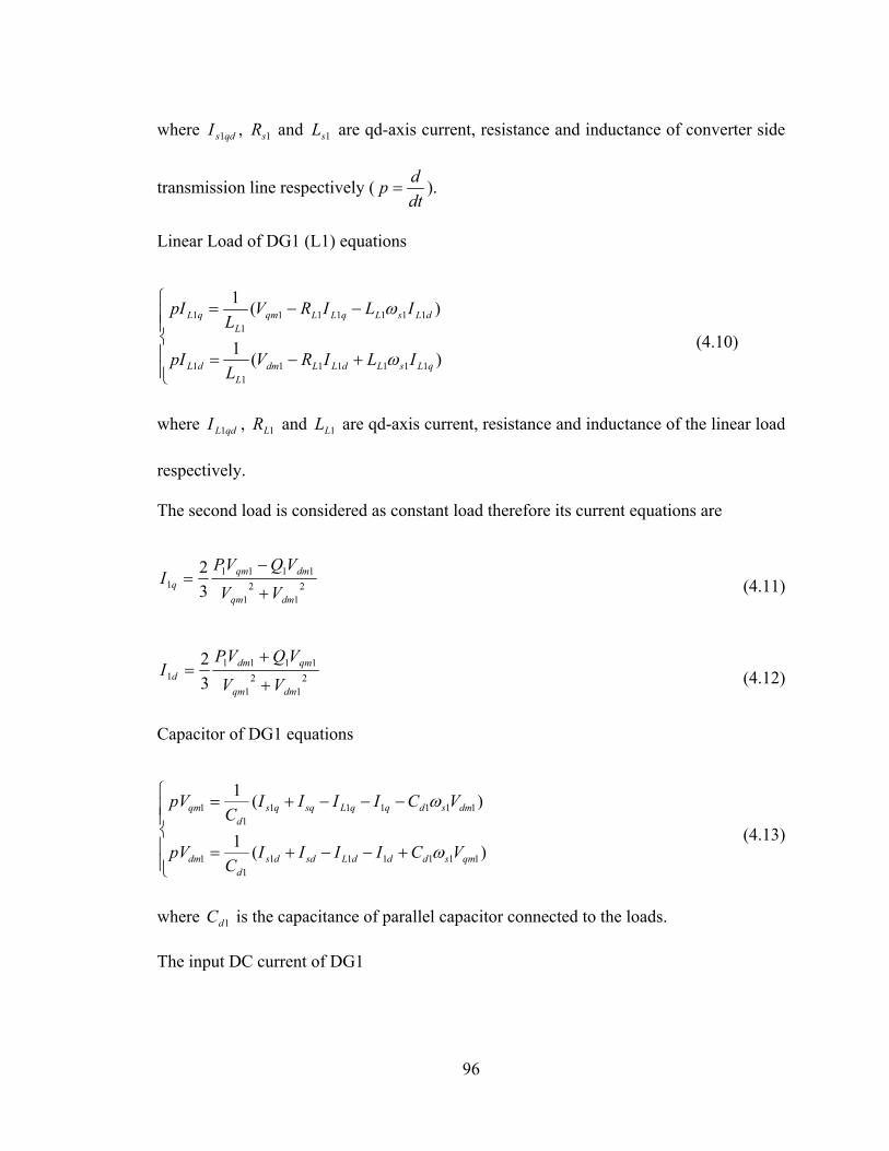
96
where qdsI 1 , 1sR and 1sL are qd-axis current, resistance and inductance of converter side
transmission line respectively (dt
dp ).
Linear Load of DG1 (L1) equations
)(1
)(1
1111111
1
1111111
1
qLsLdLLdmL
dL
dLsLqLLqmL
qL
ILIRVL
pI
ILIRVL
pI
(4.10)
where qdLI 1 , 1LR and 1LL are qd-axis current, resistance and inductance of the linear load
respectively.
The second load is considered as constant load therefore its current equations are
21
21
11111 3
2
dmqm
dmqmq
VV
VQVPI
(4.11)
21
21
11111 3
2
dmqm
qmdmd
VV
VQVPI
(4.12)
Capacitor of DG1 equations
)(1
)(1
1111111
1
1111111
1
qmsdddLsddsd
dm
dmsdqqLsqqsd
qm
VCIIIIC
pV
VCIIIIC
pV
(4.13)
where 1dC is the capacitance of parallel capacitor connected to the loads.
The input DC current of DG1

97
)(4
311111 dsdqsqinpv IMIMII (4.14)
)(4
311111 dsdqsqinpv IMIMII (4.15)
The nonlinear model of the PV system relating the current flowing out of the PV and the
terminal voltage is defined as follows:
1)exp(
s
pvrspphppv n
V
Ak
qInInI
(4.16)
100
)(S
kII rsrcph (4.17)
4.3 Steady-State Operation
At steady state the derivatives of the states in the dynamic equations are set equal
to zero. The converter equations of DG1
2
2
11111111
11111111
dcdqssdssdmds
dcqdssqssqmqs
VMILIRVV
VMILIRVV
(4.18)
Linear Load of DG1 (L1) equations
qLLdLLdm
dLLqLLqm
ILIRV
ILIRV
11111
11111
(4.19)
Capacitor of DG1 equations
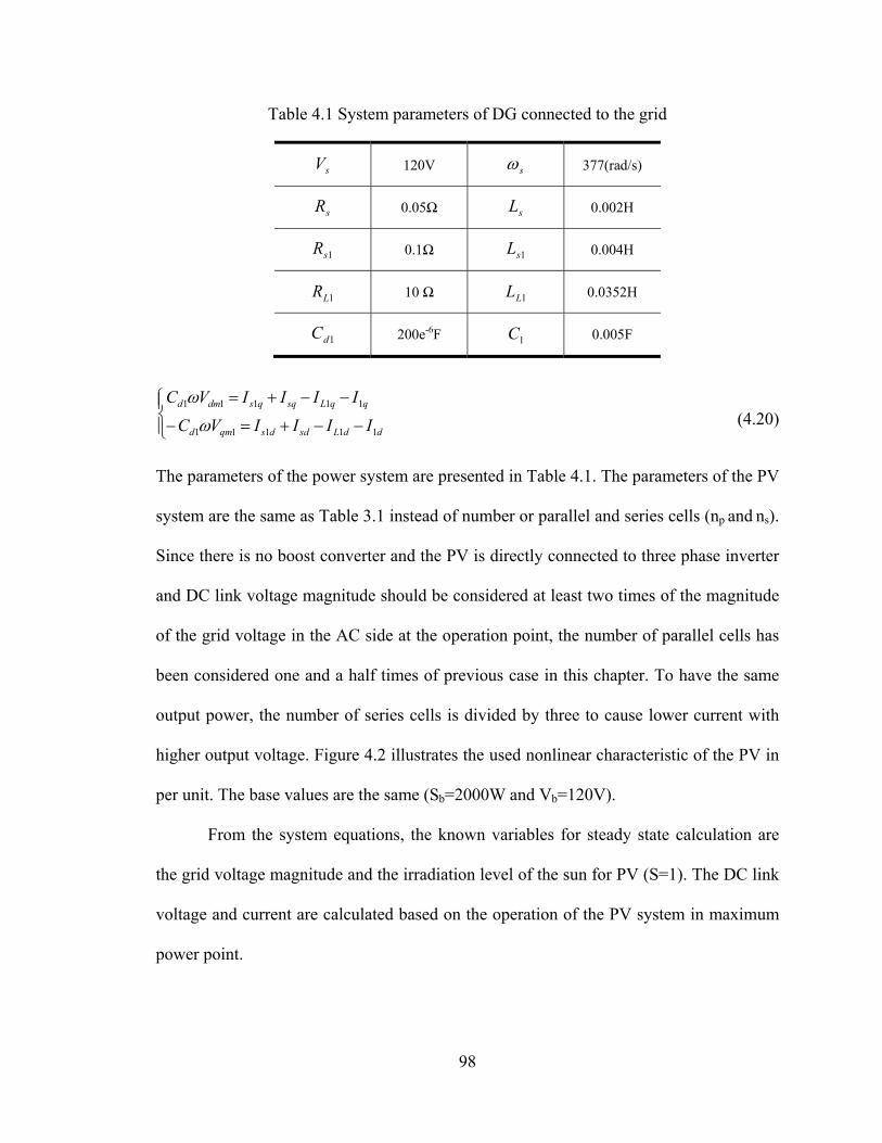
98
Table 4.1 System parameters of DG connected to the grid
sV 120V s 377(rad/s)
sR 0.05Ω sL 0.002H
1sR 0.1Ω 1sL 0.004H
1LR 10 Ω 1LL 0.0352H
1dC 200e-6F 1C 0.005F
ddLsddsqmd
qqLsqqsdmd
IIIIVC
IIIIVC
11111
11111
(4.20)
The parameters of the power system are presented in Table 4.1. The parameters of the PV
system are the same as Table 3.1 instead of number or parallel and series cells (np and ns).
Since there is no boost converter and the PV is directly connected to three phase inverter
and DC link voltage magnitude should be considered at least two times of the magnitude
of the grid voltage in the AC side at the operation point, the number of parallel cells has
been considered one and a half times of previous case in this chapter. To have the same
output power, the number of series cells is divided by three to cause lower current with
higher output voltage. Figure 4.2 illustrates the used nonlinear characteristic of the PV in
per unit. The base values are the same (Sb=2000W and Vb=120V).
From the system equations, the known variables for steady state calculation are
the grid voltage magnitude and the irradiation level of the sun for PV (S=1). The DC link
voltage and current are calculated based on the operation of the PV system in maximum
power point.
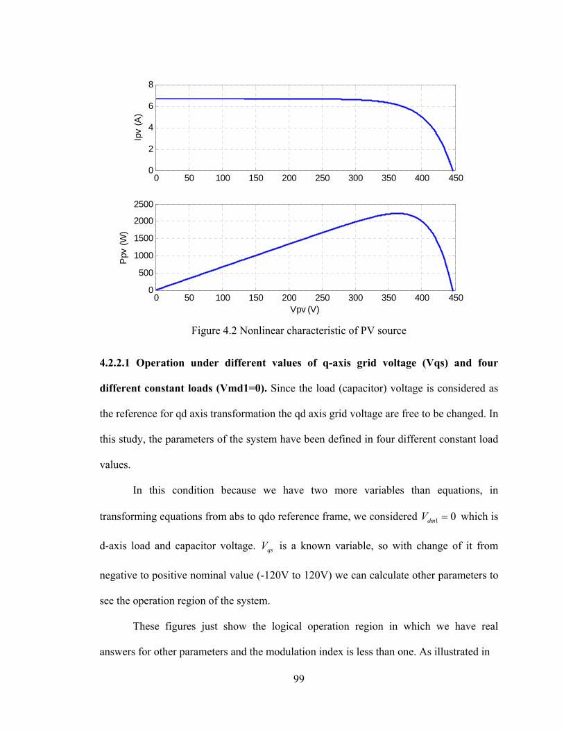
99
0 50 100 150 200 250 300 350 400 4500
2
4
6
8
Ipv
(A)
0 50 100 150 200 250 300 350 400 4500
500
1000
1500
2000
2500
Vpv (V)
Ppv
(W
)
Figure 4.2 Nonlinear characteristic of PV source
4.2.2.1 Operation under different values of q-axis grid voltage (Vqs) and four
different constant loads (Vmd1=0). Since the load (capacitor) voltage is considered as
the reference for qd axis transformation the qd axis grid voltage are free to be changed. In
this study, the parameters of the system have been defined in four different constant load
values.
In this condition because we have two more variables than equations, in
transforming equations from abs to qdo reference frame, we considered 01 dmV which is
d-axis load and capacitor voltage. qsV is a known variable, so with change of it from
negative to positive nominal value (-120V to 120V) we can calculate other parameters to
see the operation region of the system.
These figures just show the logical operation region in which we have real
answers for other parameters and the modulation index is less than one. As illustrated in

100
Figure 4.3, the operation region of the system based on predefined values of the loads and
grid impedances is in a narrow range of q-axis main grid voltage in which with change of
qsV from 118V to 120V, load voltage ( 1qmV ) changes from 70V to 140V. Figure 4.4
shows with increasing grid and load voltage, modulation index of the converter increases
gradually. Active power of the converter is constant because its input DC voltage and
current are assumed to be constant. In low constant load, because output active power of
the converter is more than total load, excessive power flows into the grid. In addition
because the range of the change of qsV is small but 1qmV is increasing, the difference
between them decreases gradually which causes reduction in active power consumed by
line resistances although active power of the linear load due to increase of its voltage
increases, therefore active power that is flowing into the main grid in Figure 4.5
(magnitude) first starts to increase then it reduces.
As can be seen from the figures, change of the constant load active power has
more effect than change of the constant load reactive power on operation region. With
119.7 119.75 119.8 119.85 119.9 119.95 12060
70
80
90
100
110
120
130
140
Vqs
Vqm
1
P1=800W, Q1=200Var
P1=1600W, Q1=200Var
P1=800W, Q1=400Var
P1=1600W, Q1=400Var
119.7 119.75 119.8 119.85 119.9 119.95 1200.1
0.2
0.3
0.4
0.5
0.6
0.7
0.8
0.9
1
Vqs
M1
P1=800W, Q1=200Var
P1=1600W, Q1=200Var
P1=800W, Q1=400Var
P1=1600W, Q1=400Var
Figure 4.3 Load and capacitor voltage Figure 4.4 Modulation index magnitude
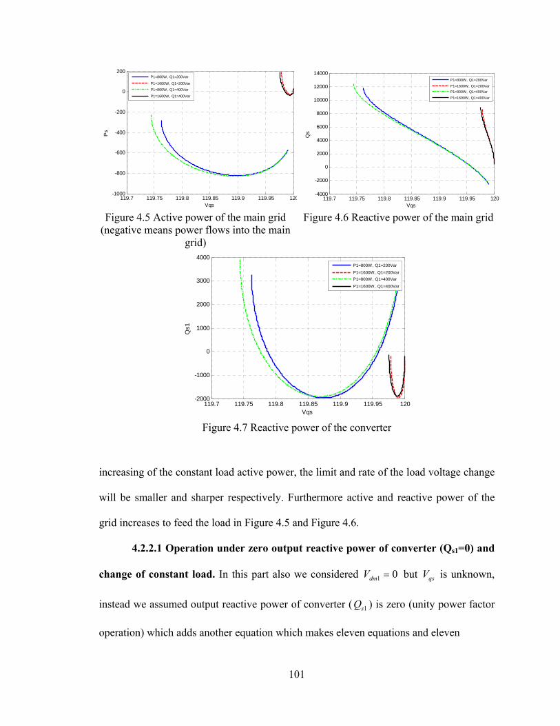
101
119.7 119.75 119.8 119.85 119.9 119.95 120-1000
-800
-600
-400
-200
0
200
Vqs
Ps
P1=800W, Q1=200Var
P1=1600W, Q1=200Var
P1=800W, Q1=400Var
P1=1600W, Q1=400Var
119.7 119.75 119.8 119.85 119.9 119.95 120-4000
-2000
0
2000
4000
6000
8000
10000
12000
14000
Vqs
Qs
P1=800W, Q1=200Var
P1=1600W, Q1=200Var
P1=800W, Q1=400Var
P1=1600W, Q1=400Var
Figure 4.5 Active power of the main grid (negative means power flows into the main
grid)
Figure 4.6 Reactive power of the main grid
119.7 119.75 119.8 119.85 119.9 119.95 120-2000
-1000
0
1000
2000
3000
4000
Vqs
Qs1
P1=800W, Q1=200Var
P1=1600W, Q1=200Var
P1=800W, Q1=400Var
P1=1600W, Q1=400Var
Figure 4.7 Reactive power of the converter
increasing of the constant load active power, the limit and rate of the load voltage change
will be smaller and sharper respectively. Furthermore active and reactive power of the
grid increases to feed the load in Figure 4.5 and Figure 4.6.
4.2.2.1 Operation under zero output reactive power of converter (Qs1=0) and
change of constant load. In this part also we considered 01 dmV but qsV is unknown,
instead we assumed output reactive power of converter ( 1sQ ) is zero (unity power factor
operation) which adds another equation which makes eleven equations and eleven

102
0.792
0.794
0.7940.794
0.796
0.7960.796
0.798
0.7980.798
0.8
0.80.8
0.802
0.8020.802
0.8040.804
Q1
P1
M1
50 100 150 200 250 300 350 400
200
400
600
800
1000
1200
1400
160011
9.2
119.4
119.4
119.4
119.6
119.6
119.6
119.8
119.8
119.8
120
120
120
120.2
120.2
120.2
120.4
120.4
120.4
120.6
120.6
120.6
120.8
120.8
120.8
121
121
Q1
P1
Vqm1
50 100 150 200 250 300 350 400
200
400
600
800
1000
1200
1400
1600
Figure 4.8 Modulation index magnitude of converter
Figure 4.9 Load and capacitor voltage
119.84 119.84 119.84119.86 119.86 119.86119.88 119.88 119.88119.9 119.9 119.9
119.92 119.92 119.92119.94 119.94 119.94119.96 119.96 119.96
119.98 119.98 119.98
Q1
P1
Vqs
50 100 150 200 250 300 350 400
200
400
600
800
1000
1200
1400
16000 0 0 0
1 1 1 1
2 2 2 2
3 3 3 3
4 4 4 4
5 5 5 5
6 6 6 6
Q1
P1
Vds
50 100 150 200 250 300 350 400
200
400
600
800
1000
1200
1400
1600
Figure 4.10 q-axis voltage of main grid Figure 4.11 d-axis voltage of main grid
variables. The contours of change of system parameters with change of active and
reactive power of constant load are presented. The active and reactive powers of the
constant load have been changed from 10W to 1600W and 10Var to 400Var respectively.
With a load voltage close to rated value, the modulation index is high in Figure
4.8 (about 0.8) and the output current of the converter to feed the load is small. The Load
voltage magnitude (Vm1=Vm1q) and q-axis voltage of the grid in Figure 4.9 and Figure
4.10 are close to nominal value (120V) and d-axis voltage of the main grid in Figure 4.11
is small.

103
-1400 -1400 -1400
-1200 -1200 -1200
-1000 -1000 -1000
-800 -800 -800
-600 -600 -600
-400 -400 -400
-200 -200 -200
0 0 0 0
Q1
P1
Ps
50 100 150 200 250 300 350 400
200
400
600
800
1000
1200
1400
1600
-200
-150
-150
-100
-100
-100
-50
-50
-50
00
0
50
5050
100
100
100 15
0
150
150 20
020
0
200
250
Q1
P1
Qs
50 100 150 200 250 300 350 400
200
400
600
800
1000
1200
1400
1600
Figure 4.12 Active power of main grid Figure 4.13 Reactive power of main grid
12.84
12.84
12.86
12.86
12.86
12.88
12.88
12.88
12.9
12.9
12.9
12.92
12.92
12.92
12.94
12.94
12.94
12.96
12.96
12.96
12.98
12.98
12.98
13
1313
13.02
Q1
P1
Iqs1
50 100 150 200 250 300 350 400
200
400
600
800
1000
1200
1400
1600
13
13.02
13.02
13.04
13.04
13.04
13.06
13.06
13.06
13.08
13.08
13.08
13.1
13.1
13.1
13.12
13.12
13.12
13.14
13.14
13.14
13.16
13.16
13.16
13.18
13.18
13.18
13.2
13.2
Q1
P1
Is1
50 100 150 200 250 300 350 400
200
400
600
800
1000
1200
1400
1600
Figure 4.14 q-axis output converter current Figure 4.15 Output converter current
magnitude The change of the load voltage and therefore the modulation index and converter
current magnitude is small in this range of the load change. With increasing active and
reactive power of the constant load, active and reactive power of the main grid in Figure
4.12 and Figure 4.13 increase from negative to positive values because in small loads,
output power of the converter is more than total loss and loads but with increasing the
total load will finally be more than the power of the converter and excessive load should
be fed from the main grid.

104
Output reactive power of the converter is always zero and output active power of the
converter is always at maximum power point operation of the PV source. Output current
of the inverter in Figure 4.15 is about 13A which is mostly aligned with q-axis in Figure
4.14.
4.4 Bifurcation Analysis
Power systems consist of nonlinear elements. The dynamics of these systems are
usually represented by dynamic and algebraic equations of generators or sources, loads
and transmission lines. Therefore we have a set of nonlinear differential equations where
change of some parameters of the system like loads may cause qualitative changes at
bifurcation points. Hopf bifurcation and saddle node bifurcation are the typical
bifurcations. The saddle node bifurcation point results in instability. Hopf bifurcation
causes oscillatory behavior of a power system [116].
In this part, the CL_MATCONT software package [110] along with MATLAB is
used. The equilibrium curve and bifurcation points of a PV system with consideration of
nonlinear behavior of input source are investigated. For this purpose all of the parameters
are transformed to per unit values. The base values for calculating parameter values in
per unit are as follows:
VASb 2000 , VVb 120 , )(3
2
b
bb V
SI , )(
2
3 2
b
bb S
VZ , )/(377 sradb (4.21)
Figure 4.16 shows DC voltage of a PV source versus active power of constant
load (P1) as an active parameter for different q-axis converter modulation indices. With

105
Figure 4.16 Equilibrium curve of PV DC voltage when constant load active power (P1) is an active parameter for different q-axis modulation indices. H (Hopf Bifurcation Point),
LP (Limit Point).
Figure 4.17 Equilibrium curve of the main grid active power (Ps) when constant load active power (P1) is an active parameter for different q-axis modulation indices.

106
Figure 4.18 Equilibrium curve of the main grid reactive power (Qs) when constant load active power (P1) is an active parameter for different q-axis modulation indices.
Figure 4.19 Equilibrium curve of the input power (Pin) when constant load active power (P1) is an active parameter for different q-axis modulation indices.
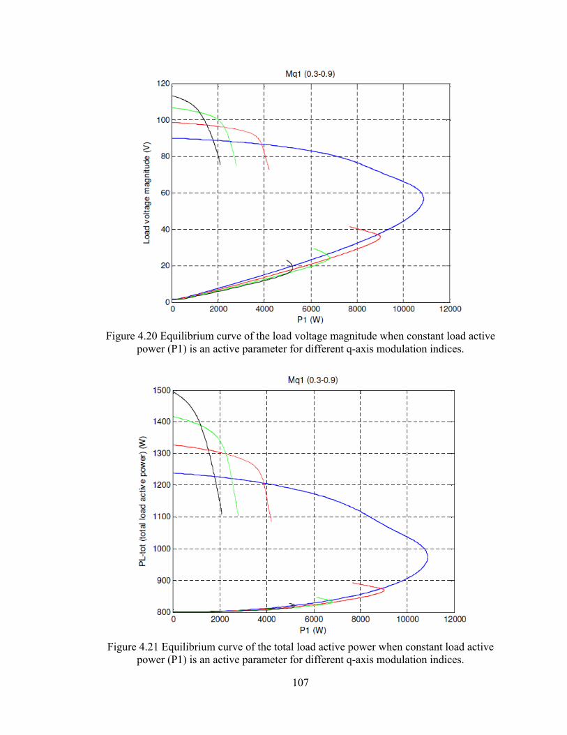
107
Figure 4.20 Equilibrium curve of the load voltage magnitude when constant load active power (P1) is an active parameter for different q-axis modulation indices.
Figure 4.21 Equilibrium curve of the total load active power when constant load active power (P1) is an active parameter for different q-axis modulation indices.
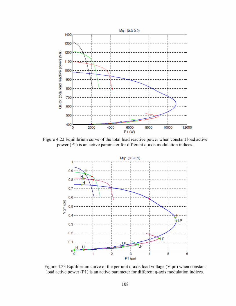
108
Figure 4.22 Equilibrium curve of the total load reactive power when constant load active power (P1) is an active parameter for different q-axis modulation indices.
Figure 4.23 Equilibrium curve of the per unit q-axis load voltage (Vqm) when constant load active power (P1) is an active parameter for different q-axis modulation indices.

109
Figure 4.24 Equilibrium curve of the converter output voltage magnitude when constant load active power (P1) is an active parameter for different q-axis modulation indices.
increase of load active power with a constant PV DC voltage more modulation index is
needed and with increase of DC voltage in a constant load active power, modulation
index is reduced. Moreover with a higher modulation index, the operation region of PV
DC voltage increases and operation region of load active power is decreased. Hopf
bifurcation and limit points in equilibrium curves are defined.
Figure 4.17 and Figure 4.18 illustrate equilibrium curves of the main grid’s active
and reactive powers versus load active power. The grid is always producing reactive
power. With lower active power of load, excessive power of the converter flows into the
main grid and makes it active power negative.
In Figure 4.19 we can get maximum power from the input source in all
modulation indices with different combinations of load active power and therefore PV

110
DC voltage. Figure 4.20 shows the operation region can be either in less active power of
the load and higher load voltage or in more load active power and lower load voltage.
Because the active and reactive power of the RL load are just related to its
voltage, the trend of powers of total load in Figure 4.21 and Figure 4.22 that are a
combination of linear RL load and constant load are like voltage magnitude. In higher
load voltage, near nominal value that is usually acceptable operation region, with increase
of constant load active, power active and reactive power of RL load and therefore total
load is reduced.
Figure 4.23 shows per unit q-axis voltage of the load versus active power of the
constant load. The trend of change of this figure is similar to Figure 4.20 because d-axis
voltage of load is always small. Also in this figure, bifurcation points are defined. Figure
4.24 illustrates converter output voltage equilibrium curves. In each iteration PV DC
voltage is a state variable and modulation index is constant therefore trend of output
converter voltage is like DC voltage. As it is shown, in a constant load, with increase of
modulation index we have more converter output converter voltage. In a constant output
voltage with reduction of modulation index we can feed more load because we are
increasing output converter current with a constant voltage indirectly.
4.5 Controller Design
Since the DG system is connected to the main grid and the voltage magnitude and
frequency are adapted from it, two objectives can be considered for the controller design
purposes.

111
First the output active and reactive power of three phase inverter can be
controlled. In this case the assumption is that the input power of the DG is always equal
or bigger than the reference so it can send the demand power from the reference all the
time. In this case
21
21
1*
11*
1*1 3
2
dmqm
dmsqmsqs
VV
VQVPI
(4.22)
21
21
1*
11*
1*1 3
2
dmqm
qmsdmsds
VV
VQVPI
(4.23)
where *1sP and *
1sQ are the reference of output active and reactive power respectively
which producing the reference of the output qd-axis current of the inverter ( *1qdsI ).
In most of real conditions and also in the studied system in this chapter, the input
source has a limit rated power. We also prefer to transfer the maximum possible power
from a renewable source like PV. Due to aforementioned reasons, the objective of the
controller is considered to control input DC link voltage and output reactive power of the
inverter.
With the control of the DC link voltage which is the same as the PV output
voltage illustrated in Figure 4.25, maximum power point tracking can be applied to
extract the maximum power from the PV system at any irradiation level of the sun. The
reactive power control can be used for unity power factor operation. If the local load
power is less than the PV source power at MPP, the excessive power will flow into the
grid and if the load is more than the PV source or it needs reactive power, the rest will be
delivered from the grid.

112
4.5.1 DC Link Voltage Control
The maximum power point operation produces the reference for the DC link
voltage. To control the DC link voltage, from its dynamic equation
)(4
3111111 dsdqsqpvdc IMIMIVsC
(4.24)
With substitution of modulation index equations
dsqssdmdqsdssqmqdc
pvdc IILVIILVV
IVsC 111111111
11 )()(2
3 (4.25)
dsdmdqsqmqdc
pvdc IVIVV
IVsC 11111
11 )()(2
3
(4.26)
dsdmdqsqmqdcpvdcdc IVIVVIsVCV 11111111 )()(2
3
(4.27)
))(()()(2
3
22
1
*211111
21
1dcdcvpvdsdmdqsqmqpvdc VVskIVIVPsV
C
(4.28)
Where )(skv is the DC voltage controller, therefore DC voltage transfer function is
)(2
)(
1*2
1
21
sksC
sk
V
V
v
v
dc
dc
(4.29)
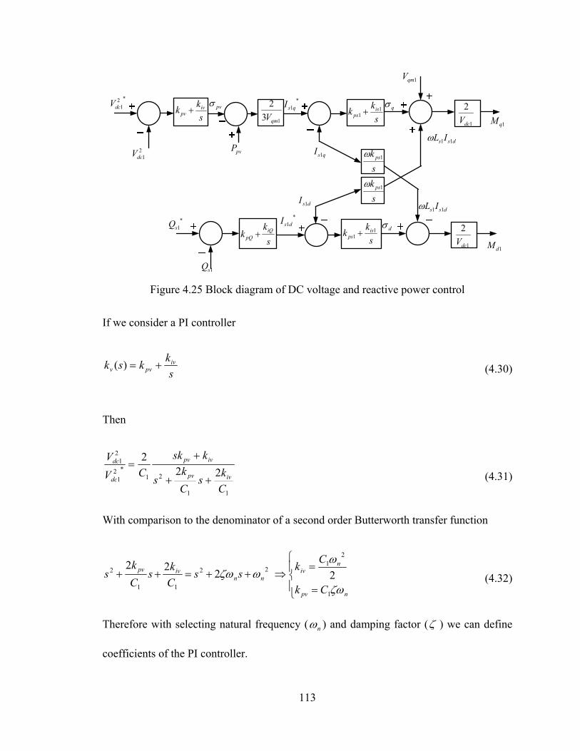
113
*1qsI
qsI 1
dss IL 11
1qmV
1
2
dcV 1qM
q
1
2
dcV
*1dsI
dsI 1
d
dss IL 11
1dM
pv
pvP
*21dcV
21dcV
*1sQ
1sQ
13
2
qmV
s
kk iQ
pQ
s
kk iv
pv s
kk is
ps1
1
s
kk is
ps1
1
s
k ps1
s
k ps1
Figure 4.25 Block diagram of DC voltage and reactive power control
If we consider a PI controller
s
kksk iv
pvv )( (4.30)
Then
11
21*2
1
21
222
C
ks
C
ks
ksk
CV
V
ivpv
ivpv
dc
dc
(4.31)
With comparison to the denominator of a second order Butterworth transfer function
22
11
2 222
nnivpv ss
C
ks
C
ks
npv
niv
Ck
Ck
1
21
2 (4.32)
Therefore with selecting natural frequency ( n ) and damping factor ( ) we can define
coefficients of the PI controller.
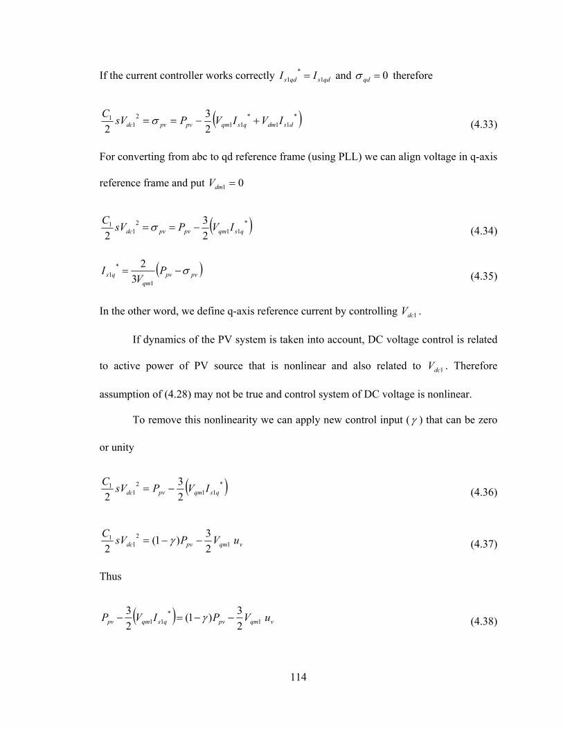
114
If the current controller works correctly qdsqds II 1*
1 and 0qd therefore
*11
*11
21
1
2
3
2 dsdmqsqmpvpvdc IVIVPsVC
(4.33)
For converting from abc to qd reference frame (using PLL) we can align voltage in q-axis
reference frame and put 01 dmV
*11
21
1
2
3
2 qsqmpvpvdc IVPsVC
(4.34)
pvpvqm
qs PV
I 1
*1 3
2 (4.35)
In the other word, we define q-axis reference current by controlling 1dcV .
If dynamics of the PV system is taken into account, DC voltage control is related
to active power of PV source that is nonlinear and also related to 1dcV . Therefore
assumption of (4.28) may not be true and control system of DC voltage is nonlinear.
To remove this nonlinearity we can apply new control input ( ) that can be zero
or unity
*11
21
1
2
3
2 qsqmpvdc IVPsVC
(4.36)
vqmpvdc uVPsVC
12
11
2
3)1(
2 (4.37)
Thus
vqmpvqsqmpv uVPIVP 1*
11 2
3)1(
2
3 (4.38)

115
_
++
pvP
vu
13
2
qmV
+
*21dcV
21dcV
13
2
qmV
*1qsI
qsI 1
dss IL 11
1qmV
1
2
dcV 1qM_
++
+
+
q
1
2
dcV
_+ +
*1dsI
dsI 1
d_
dss IL 11
1dM
*1sQ
_
+
1sQ
s
kk iQ
pQ
s
kk iv
pv s
kk is
ps1
1
s
kk is
ps1
1
s
k ps1
s
k ps1
Figure 4.26 Block diagram of DC voltage and reactive power control after removing the effect of PV source
pvqm
vqs PV
uI1
*1 3
2 (4.39)
If we choose 1 , DC voltage control is independent of active power of PV system and
the control diagram will be
pvqm
vqs PV
uI1
*1 3
2 (4.40)
))((2
3)1(
22
1
*211
21
1dcdcvvqmpvdc VVskuVPsV
C (4.41)
And if 1
))((2
3
22
1
*211
21
1dcdcvvqmdc VVskuVsV
C (4.42)

116
If s
kksk iv
pvv )( then
11
21*2
1
21
222
C
ks
C
ks
ksk
CV
V
ivpv
ivpv
dc
dc
(4.43)
If )(
)(3
21
ss
sskv then
1
2
1
123
3
21
1*2
1
21
222
Cs
Css
s
CV
V
dc
dc
(4.44)
4.5.2 Reactive Power Control
Output reactive power of the inverter after the filter at PCC
)(2
311111 qsdmdsqms IVIVQ (4.45)
If it is assumed that 01 dmV
))(())(( 1*
11*
1*
1 ssiQ
pQssQds QQs
kkQQskI (4.46)
A new variable can be defined as
)( 1*
1 ssqs QQxs (4.47)
Thus
qsiQsspQds xkQQkI )( 1*
1*
1 (4.48)
Therefore d-axis reference current can be defined using reference reactive power ( *1sQ ).
Usually *1dcV is kept constant or defined by maximum power point tracking
(MPPT) of PV system and for unity power factor 0*1 sQ

117
4.5.3 Current Control
After defining the qd-axis current references from the outer DC link voltage and
reactive power controllers, the inner current controller can be designed. From the
dynamic equation of the inverter transmission line in complex format
))((2 1
*1111
11111111 qdsqdsssqdm
dcqdqdssqdssqdss IIskV
VMIjLIRsIL (4.49)
where )(1 sks is the current controller, therefore current transfer function is
)(
)(
1111
1*
1
1
skjLRsL
sk
I
I
ssss
s
qds
qds
(4.50)
And
s
kjkksk psis
pss11
11 )(
(4.51)
where 1psk and 1isk are proportional and integral parameters of current controller.
111112
1
111
*1
1
)( psissspss
psisps
qds
qds
kjksjLRksL
kjksk
I
I
(4.52)
If it is chosen
11
11 ps
s
sis k
L
Rk (4.53)
then
11
1
1
111
11
1
*1
1
))((
)(
pss
ps
s
spss
pss
s
qds
qds
ksL
k
jL
RsksL
kjL
Rs
I
I
(4.54)

118
From (4.49)
11
1
2qdmqd
dcqd V
VM (4.55)
and
))(( 111111 s
kjkkjII psis
psddsqqss
(4.56)
dsdsdds
qsqsqqs
III
III
1*
11
1*
11 (4.57)
So for separated qd-axis from the complex format
)()(
)()(
11
1111
11
1111
s
kI
s
kkI
s
kI
s
kkI
psqqs
ispsddsds
psdds
ispsqqsqs
(4.58)
The outputs of current controller are modulation indices ( 1qdM ) that produce the
output voltage of the three phase inverter connected to the grid.
4.5.4 State Space Model
To define the state space model of the system, the dynamic equations and also the
designed controller parameters have been used. From the control part
2
)(3
2)()( 1
1111
1111
21
*21
dcqqsds
psqmsqs
qmvdcdcpv
VMVI
s
kVskI
VskVVP
(4.59)

119
2
)()()( 1111
1111
*1
dcddsqs
pssdsQss
VMVI
s
kskIskQQ
(4.60)
And from the dynamic equations of the system
)(2
32
)(1
)(1
)(1
)2
(1
11111
21
1
111111
1
111111
1
111111
11
1
dsdmqsqmpvdc
sqdssqdsqdmsqds
sqd
qdLLqdLLqdmL
qdL
qdmdqdqdLsqdqdsd
qdm
qdssqdssqdmdc
qds
qds
IVIVPC
sV
IjLIRVVL
sI
IjLIRVL
sI
VjCIIIIC
sV
IjLIRVV
ML
sI
(4.61)
In separated qd-axis format and with assumption of 01 dmV that is considered in
control part for decouple control of reactive power
11
21
1111
1
1
11111
1
111111
1
11111
11
1
111111
11
1
2
)(1
)(1
)(1
)(1
)(1
)2
(1
)2
(1
spvdc
qqLsqqsd
qm
sqssdssds
sd
sdssqsqmsqs
sq
qLLdLLL
dL
dLLqLLqmL
qL
qssdssdc
ds
ds
dssqssqmdc
qs
qs
PPC
sV
IIIIC
sV
ILIRVL
sI
ILIRVVL
sI
ILIRL
sI
ILIRVL
sI
ILIRV
ML
sI
ILIRVV
ML
sI
(4.62)

120
With substituting control part equations in the first two equations of plant
qsps
sssdssQssQss
ds
dssps
ssqs
sqm
pvqm
svdcqm
svdc
sqs
Is
kLRskIskskQskskQ
LsI
ILs
kRskI
skV
PV
skskVV
skskV
LsI
11
11111*
1111
1
111
111
111
1
*21
11
21
11
)()()()()()(1
)(
)(3
2
3
2)()(
3
2)()()(
1
(4.63)
In general, the state space model
dEUBUAXX and )()( 1dEUBUAsIX (4.64)
dFUDUCXY (4.65)
where X , U , dU and Y are state variable, input , disturbance input and output matrices
respectively. The complete state space model of the system is as follows:
21
1
1
1
1
1
111
1
1
1
1
11
1
1
1
1
11
1
1
1
1
111
1
1
1
1
1
11
21
1
1
1
1
1
00000000
0001
01
01
000000
01
0000
000000
01
0000
000000)(
3
2)()(00000
)(
dc
qm
sd
sq
dL
qL
ds
qs
ddd
s
s
s
s
ss
s
s
s
L
L
L
L
LL
L
L
L
s
ss
s
ps
s
s
qmssv
s
s
s
ps
s
ss
dc
qm
sd
sq
dL
qL
ds
qs
V
VI
I
I
I
I
I
CCC
L
R
L
LLL
L
L
RL
R
L
LLL
L
L
RL
Rsk
sL
k
L
L
VLsksk
L
L
sL
k
L
Rsk
V
VI
I
I
I
I
I
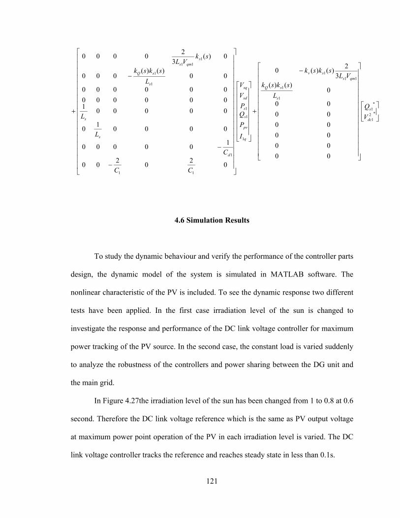
121
*21
*1
1
1
111
1
1
1
11
1
1
1
111
00
00
00
00
00
00
0)()(
3
2)()(0
02
02
00
100000
00001
0
000001
000000
000000
00)()(
000
0)(3
20000
dc
s
s
sQ
qmssv
q
pv
s
s
sd
sq
d
s
s
s
sQ
sqms
V
Q
L
skskVL
sksk
I
P
QP
V
V
CC
C
L
L
L
sksk
skVL
4.6 Simulation Results
To study the dynamic behaviour and verify the performance of the controller parts
design, the dynamic model of the system is simulated in MATLAB software. The
nonlinear characteristic of the PV is included. To see the dynamic response two different
tests have been applied. In the first case irradiation level of the sun is changed to
investigate the response and performance of the DC link voltage controller for maximum
power tracking of the PV source. In the second case, the constant load is varied suddenly
to analyze the robustness of the controllers and power sharing between the DG unit and
the main grid.
In Figure 4.27the irradiation level of the sun has been changed from 1 to 0.8 at 0.6
second. Therefore the DC link voltage reference which is the same as PV output voltage
at maximum power point operation of the PV in each irradiation level is varied. The DC
link voltage controller tracks the reference and reaches steady state in less than 0.1s.
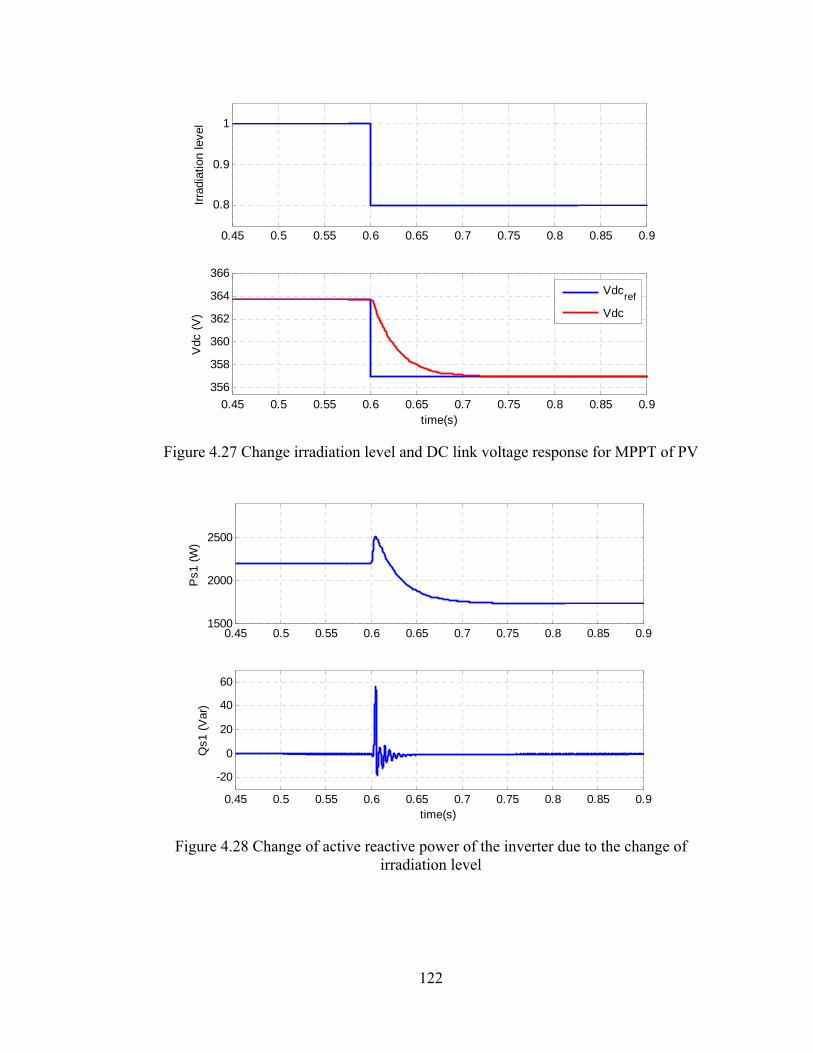
122
0.45 0.5 0.55 0.6 0.65 0.7 0.75 0.8 0.85 0.9
0.8
0.9
1
Irra
diat
ion
leve
l
0.45 0.5 0.55 0.6 0.65 0.7 0.75 0.8 0.85 0.9
356
358
360
362
364
366
time(s)
Vdc
(V
)
Vdcref
Vdc
Figure 4.27 Change irradiation level and DC link voltage response for MPPT of PV
0.45 0.5 0.55 0.6 0.65 0.7 0.75 0.8 0.85 0.91500
2000
2500
Ps1
(W
)
0.45 0.5 0.55 0.6 0.65 0.7 0.75 0.8 0.85 0.9
-20
0
20
40
60
time(s)
Qs1
(V
ar)
Figure 4.28 Change of active reactive power of the inverter due to the change of irradiation level

123
0.45 0.5 0.55 0.6 0.65 0.7 0.75 0.8 0.85 0.9-1500
-1000
-500
0
Ps
(W)
0.45 0.5 0.55 0.6 0.65 0.7 0.75 0.8 0.85 0.9-1600
-1500
-1400
-1300
-1200
time(s)
Qs
(Var
)
Figure 4.29 Change of active reactive power of the main grid due to the change of irradiation level
0.45 0.5 0.55 0.6 0.65 0.7 0.75 0.8 0.85 0.98
10
12
14
Is1q
(A
)
Is1qref
Is1q
0.45 0.5 0.55 0.6 0.65 0.7 0.75 0.8 0.85 0.9-0.02
-0.01
0
0.01
0.02
time(s)
Is1d
(A
)
Is1d
ref
Is1d
Figure 4.30 Reference and actual qd-axis currents of inverter

124
0.45 0.5 0.55 0.6 0.65 0.7 0.75 0.8 0.85 0.90.68
0.7
0.72
0.74
Mq
0.45 0.5 0.55 0.6 0.65 0.7 0.75 0.8 0.85 0.9-0.16
-0.14
-0.12
-0.1
-0.08
-0.06
time(s)
Md
Figure 4.31 qd-axis modulation indices of the inverter
Figure 4.28 illustrates the output active and reactive power of the inverter. The
active power reduces due to the reduction of irradiation level but still extracts the
maximum possible power from the sun. The reference for reactive power controller is
chosen to be zero for unity power factor operation of the PV system. Instead of small
fluctuations in the instant of the irradiation level change, the output reactive power is
always kept at zero. Since the loads are less than the output power of the DG unit, the
power of the main grid is negative in Figure 4.29. It means the excessive power is
transferred to the main network.
Although the inverter is not producing reactive power, the big value of capacitor
is the reason of negative reactive power of the grid. With reduction of the irradiation level
and consequently the output power of the DG, the transferred power to the grid in the
constant load is also reduced. Figure 4.30 shows how the current controllers are trying to
125
follow qd-axis reference currents. The d-axis reference current corresponding to the
reactive power is zero for all time. The q-axis reference current is changing based on the
output of DC link voltage controller. The faster speed of the inner current controllers for
tracking the references compared to outer controller is shown in this figure. In Figure
4.31 the modulation indices of the three phase inverter are presented. It shows that due to
the performance of the controllers the inverter is always operating in linear region
without saturation of the modulation index magnitude.
In the second case, the active and reactive powers of the constant load are
changed in two different instances in Figure 4.32. The active power of the load is change
from 800W to 2400W at 0.6s and reactive power is changed from 200Var to 600Var at
0.8s respectively. Due to the constant irradiation level and MPP operation, the output
active power of the DG is constant. The additional power of the load when it is raised
beyond the maximum power of the PV, should then come from the grid. The active
power of the grid is changed from negative (absorbing power) to positive (producing
power). Due to the increase of the load reactive power at 0.8s, the flow of the reactive
power into the grid reduces and goes into the load instead. Although there is no load
voltage control, load voltage magnitude is dictated by the grid and shows just a small
change. The phase lock loop always tracks the frequency and the angle of the load
voltage and makes the d-axis load voltage zero. DC link voltage is also tracking its
reference even with a significant change in the load values.

126
4.1 Conclusions
In this chapter, the steady state operation region of a microgrid with a PV source
connected to the main network is studied. First, with changing of the q-axis grid voltage,
other parameters are calculated. The operation region of the grid voltage is small in that it
is always close to rated value. With a small change in q-axis main grid voltage we will
have a wide change in load voltage. With increasing the load and grid voltages,
modulation index of the converter increases and it is always less than one. The change of
the reactive power of the grid and converter are based on difference between the grid and
the converter voltages as well as voltage of the capacitor which produces part of reactive
power. For the second case, output reactive power of the converter is considered zero so
we will have two operation regions based on the load voltage magnitude. For bigger load
voltage, modulation index is also bigger and in constant input DC voltage and current,
output converter current is smaller. With increasing active and reactive power of constant
load, active and reactive power of the grid increases because output powers of the
converter are assumed constant always operating at maximum power point of PV source
in this condition.
The controllers are design and explained in detail for the system. The load voltage
magnitude and frequency are adapted from the main grid. The DC link voltage is
controlled for maximum power point operation of the PV. For unity power factor
operation the second reference has been considered as output reactive power of the three
phase inverter. Inner current control loops are designed to control qd-axis output currents
of the converter separately. To control the DC link voltage, the nonlinear characteristic of

127
0.5 0.6 0.7 0.8 0.9 1
1000
2000
3000
a)P
1 (W
)
0.5 0.6 0.7 0.8 0.9 1
200400600800
b)Q
1 (V
ar)
0.5 0.6 0.7 0.8 0.9 1-1000
0
1000
c)P
s (W
)
0.5 0.6 0.7 0.8 0.9 1-1500
-1000
-500
d)Q
s (V
ar)
0.5 0.6 0.7 0.8 0.9 1-20
0
20
e)Q
s1 (
Var
)
0.5 0.6 0.7 0.8 0.9 1110
120
130
f)V
m1q
(V
)
0.5 0.6 0.7 0.8 0.9 1-5
0
5
g)V
m1d
(V
)
0.5 0.6 0.7 0.8 0.9 1
362
364
time(s)
h)V
dc (
V)
Vdcref
Vdc
Figure 4.32 system dynamic under the change of constant load, a) constant load active power, b)constant load reactive power, c) active power of the main grid, d) reactive
power of the main grid, e) reactive power of the inverter f) q-axis load voltage g) d-axis load voltage h) DC link voltage.

128
the PV system is considered and using a feed forward gain, its effect on the control part is
removed. Effect of the main grid and both linear and constant loads are considered in an
input output feedback linearization control. A state space model of whole system after
applying controller parts is defined. The bifurcation analysis using MATCONT software
is applied to the system. Equilibrium curves of parameters along with bifurcation points
are defined.
The dynamic system is simulated in MATLAB software. With the change of
irradiation level, DC link voltage and reactive power controllers follow their references
precisely. Even during sudden change of the loads, the actual parameters of the system
are still tracking their references well due to the fast response of the controllers. The DG
unit is always operating in unity power factor and modulation indices of the inverter,
even during transients, are less than unity.

129
CHAPTER 5
5.EXPERIMENTAL SETUP AND DYNAMIC CONTROL OF PV
SYSTEM
5.1 Introduction
To verify the proposed controllers, besides the dynamic simulation of the system,
the experimental setup has been built and tested. The system consists of a microgrid with
two different sources, a nonlinear PV and a battery source. In addition it includes three
different power electronic converters, a unidirectional DC/DC boost converter, a
bidirectional buck and boost converter and a three phase inverter. Each converter has its
own controller signals coming from different controller structures, drivers and sensor
boards. Due to the complexity of the system, each part is investigated separately and the
process of design and experimental results are shown in different sections.
5.2 Design and Open Loop Test of the Boost Converter for PV System Applications
Power electronic converters can be used to connect renewable energy sources to
the load or the grid. Using DC/DC converters it is possible to control the output voltage
magnitude and also, as a special case, obtain maximum power from renewable sources.
The photovoltaic is one the most popular methods for producing electricity from
solar energy. It directly converts the solar irradiation to electric voltage. Renewable
energies have two main advantages. First of all they are environmental friendly.

130
Secondly, there are no costs beyond manufacturing and installation. To get these benefits,
renewable energies should be used to obtain the maximum possible power from them.
Even a series array of solar cells doesn’t have enough voltage magnitude to be
directly connected to the load; therefore, a boost converter can be used to increase the
output voltage. In this section, a 3kW boost converter is designed in detail and the open
loop test validates the performance of operation.
As it is shown in Figure 5.1, the boost converter consists of five major parts
a) The Input capacitor
b) The switch
c) The diode
d) The Output capacitor
e) The inductor
Each of them should be designed and selected from the available equipment in the
market. For designing the DC/DC converter, first the rated parameters of the converter
should be defined. A 3kw DC/DC converter which operates in the switching frequency of
50kHz in considered. The output voltage is always kept constant at 300V and the input
voltage can change from 50V to 200V.
kHzf
kWP
sw 50
3 (5.1)
VV
VVV
out
in
300
20050 (5.2)

131
Figure 5.1 Schematic diagram of a boost converter
For the boost converter
DV
V
in
out
1
1 (5.3)
Therefore, the maximum duty ratio is
84.0300
5011 (min)
max out
in
V
VD (5.4)
where D is the duty ratio of the boost converter.
The ripple of the current is considered as 10 percent of the input current and the
maximum output current can be calculated as
AII
AV
VII
AI
inLpp
out
ininout
in
5.11.0
10
15
(max)
(max)(max)(max)
(max)
(5.5)
where LppI is the peak to peak ripple current. The design of the boost converter is given
in the next section after all parameters are define.
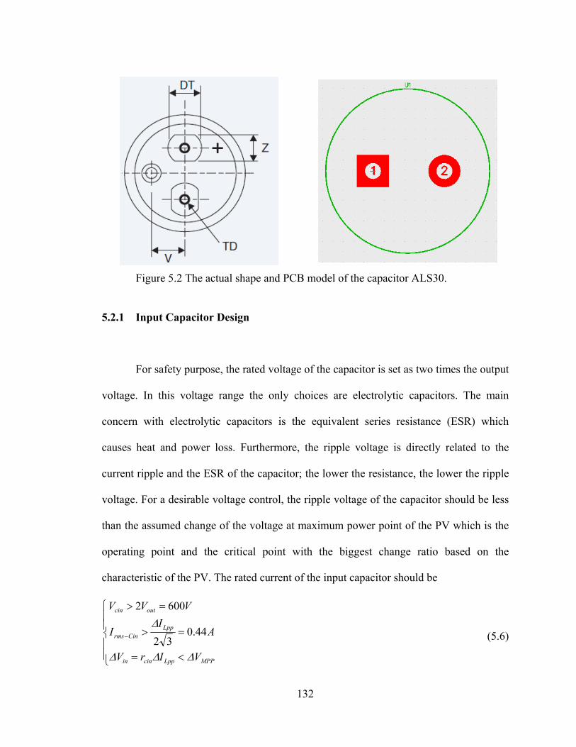
132
Figure 5.2 The actual shape and PCB model of the capacitor ALS30.
5.2.1 Input Capacitor Design
For safety purpose, the rated voltage of the capacitor is set as two times the output
voltage. In this voltage range the only choices are electrolytic capacitors. The main
concern with electrolytic capacitors is the equivalent series resistance (ESR) which
causes heat and power loss. Furthermore, the ripple voltage is directly related to the
current ripple and the ESR of the capacitor; the lower the resistance, the lower the ripple
voltage. For a desirable voltage control, the ripple voltage of the capacitor should be less
than the assumed change of the voltage at maximum power point of the PV which is the
operating point and the critical point with the biggest change ratio based on the
characteristic of the PV. The rated current of the input capacitor should be
MPPLppcinin
LppCinrms
outcin
VIrV
AI
I
VVV
44.0
32
6002
(5.6)
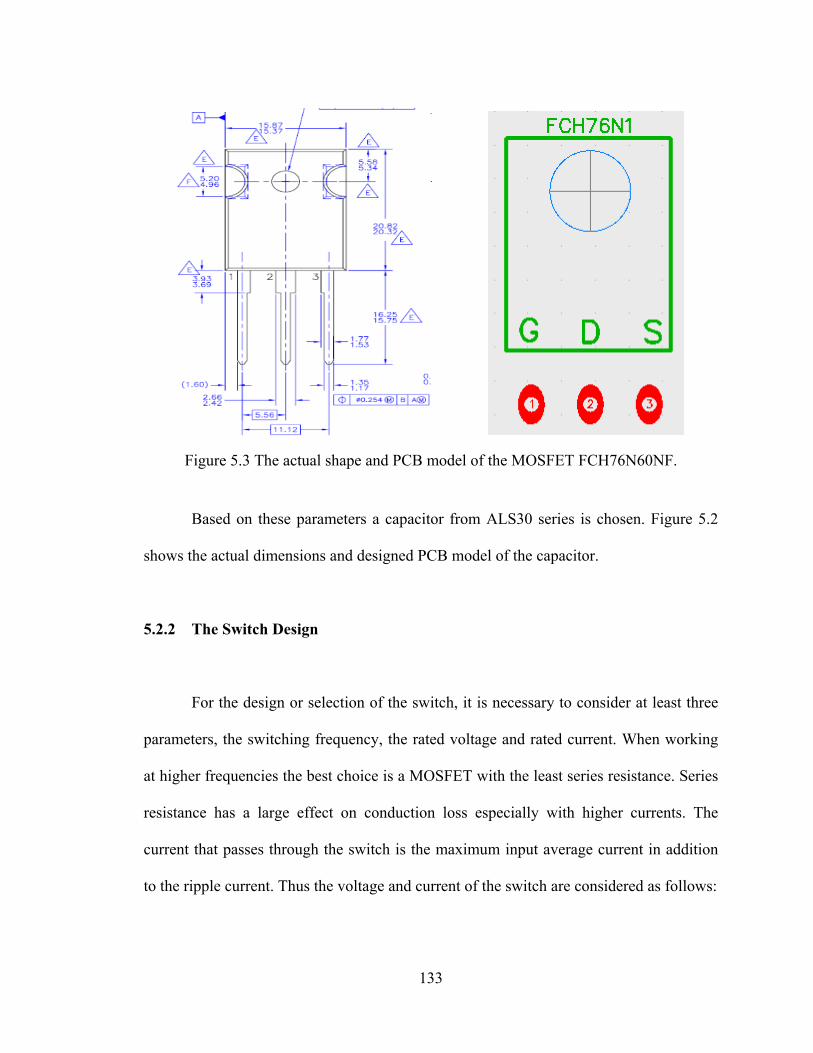
133
Figure 5.3 The actual shape and PCB model of the MOSFET FCH76N60NF.
Based on these parameters a capacitor from ALS30 series is chosen. Figure 5.2
shows the actual dimensions and designed PCB model of the capacitor.
5.2.2 The Switch Design
For the design or selection of the switch, it is necessary to consider at least three
parameters, the switching frequency, the rated voltage and rated current. When working
at higher frequencies the best choice is a MOSFET with the least series resistance. Series
resistance has a large effect on conduction loss especially with higher currents. The
current that passes through the switch is the maximum input average current in addition
to the ripple current. Thus the voltage and current of the switch are considered as follows:

134
Figure 5.4 The actual shape and PCB model of the diode STTH30L06.
AI
II
VVV
Lppinsw
outsw
75.152
6002
(max)
(5.7)
For the highest efficiency the MOSFET FCH76N60NF from Fairchild
semiconductor with low on resistance is chosen. The model of the MOSFET is presented
in Figure 5.3.
5.2.3 The Diode Design
Diode should have the same voltage rating as the switch. The current passes
through the diode is the maximum output current and the ripples. In the boost converter
the output current is always less than the input current. The current and the voltage of the
diode should be as follows:

135
AI
II
VVV
Lppoutdiod
outdiod
75.102
6002
(max)
(5.8)
The STTH30L06, the selected diode is a fast high current and high voltage diode
from STMicroelectronics. The designed model of the diode is illustrated in Figure 5.4.
5.2.4 Output Capacitor Design
Like the input capacitor, the rated and ripple voltages should be considered for the
output capacitor. The ripple voltage of the output capacitor is transmitted to the output.
So for higher waveform quality, the output ripple voltage is assumed to be around 2
percent of the output voltage which limits the selection of the capacitor with lowest ESR.
swout
outout
outCoutrms
outLppCoutout
outCout
fV
DIC
D
DII
VVIrV
VVV
)1
max(
602.0
6002
(5.9)
The output capacitor is chosen identical to the input capacitor.
5.2.5 The Inductor Design
The inductor is the most difficult component to find in the market while fulfilling
the design requirements. After defining the current rating and the inductance, the inductor
needs to be designed and its core wounded like a transformer. Usually the inductor is
assigned with the ripple current and amount of energy it can handle based on the time

136
step and current magnitude. The higher the inductance the lower the current ripple will
be.
AI
II
mHefI
DVL
LppinsatL
swLpp
in
75.15)2
(
56.050*5.1
84.0*50
(max)
3
max(min)
(5.10)
The selected core for this application is ferrite EE65/32/27, and the wire is a Litz wire
with AWG36 and 200 strands. Based on the designed inductor parameters in
52
4404.2 cmk
Ek
eg
(5.11)
The peak current
AI
II dcdcpk 16
2
(5.12)
The energy that the inductor can handle is
sWLIE pk /07168.02
1 2 (5.13)
The electrical condition coefficient
324 1054.2145.0 eBPek moe (5.14)
where mB is the operating flux density.
The core geometry coefficient
52
4404.2 cmk
Ek
eg
(5.15)

137
Table 5.1 Parameters of the designed inductor
L 0.00056H dcI 15A
dcI 2A oP 3000W
1% swf 50KHz
mB 0.3 tesla uk 0.4
rT c25
where is regulation factor.
The core that is selected (based on gk ) that is EE65/32/27 has an area product (the
product of window area and core cross section area)
49.29 cmAp (5.16)
The current density
24
/4002
cmAkAB
EeJ
upm
(5.17)
where uk is window utilization.
The rms current
13.1522 dcdcrms III (5.18)
The required bare wire area
22 782.303782.0 mmcmJ
IA rms
w (5.19)
The relationship between n AWG (American Wire Gauge) and diameter of the
wire is

138
mmdn
39
36
92*127.0
(5.20)
and the area is
2
4dA
(5.21)
Therefore the required AWG is
13n (5.22)
That is equivalent to Litz wire 36/200 for working in high frequencies. The effective
window area of the core is
2
)( 15.475.0*54.575.0 mmWW aeffa (5.23)
The number of turns is
656.0 )(
w
effa
A
WN (5.24)
Figure 5.5 shows the designed inductor. After selecting all parts a sample setup is
designed. A bulb is connected to the output as a load. A signal generator is connected to
the gate of the MOSFET to turn it on and off. In Figure 5.6, the switching signal of
50kHz with 50 percent duty ratio is applied to the gate. The input voltage is around 25V
and is boosted up around 50V based on the duty ratio.
5.2.6 PCB Model and Open Loop Test of the Boost Converter
After the design of the equipment, as illustrated in Figure 5.7, the body of the
boost converter circuit is designed. This figure shows the connection of different parts

139
Figure 5.5 The designed inductor
Figure 5.6 Input and output voltage in 50kHz switching frequency and duty ratio of 0.5
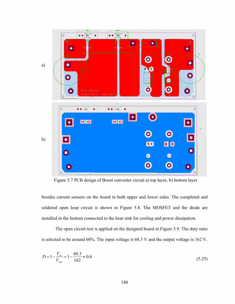
140
a)
b)
Figure 5.7 PCB design of Boost converter circuit a) top layer, b) bottom layer
besides current sensors on the board in both upper and lower sides. The completed and
soldered open loop circuit is shown in Figure 5.8. The MOSFET and the diode are
installed in the bottom connected to the heat sink for cooling and power dissipation.
The open circuit test is applied on the designed board in Figure 5.9. The duty ratio
is selected to be around 60%. The input voltage is 68.3 V and the output voltage is 162 V.
6.0162
3.6811
out
in
V
VD (5.25)
141
5.3 Closed Loop Experimental Design of Maximum Power Point Tracking
Algorithm in PV System Applications
In closed loop control of the PV source output voltage, due to nonlinear
characteristic of the solar cells and unpredictable environmental conditions and their
effects on the output of the PV panel, designing a precise controller is very complex and
sometimes not completely applicable. The most popular methods for close MPP control
of PV systems are the incremental conductance (INC) and the perturbation and
observation (P&O) algorithms.
The incremental conductance algorithm is implemented by periodically checking
the slope of the P-V curve of a PV panel. If the slope becomes zero or equal to a defined
small value, the perturbation is stopped and the PV panel is forced to work at this
operating point.
The perturbation and observation (P&O) algorithm is based on making a
perturbation in PV operation points of a PV panel in order to force the direction of
tracking toward an MPP. In this method, based on the change of measured output power
of PV in any time interval, a special amount is added to, or subtracted from the reference
voltage or duty ratio of the converter. The advantages of these two closed loop methods
are their simplicity in implementation and satisfactory accuracy without measuring solar
irradiances and temperatures.
In this section, the perturbation and observation method as closed loop MPP
controller is used to control the output power of the PV system. A programmable DC
source is used to behave like a solar system. A DC/DC boost converter is designed and
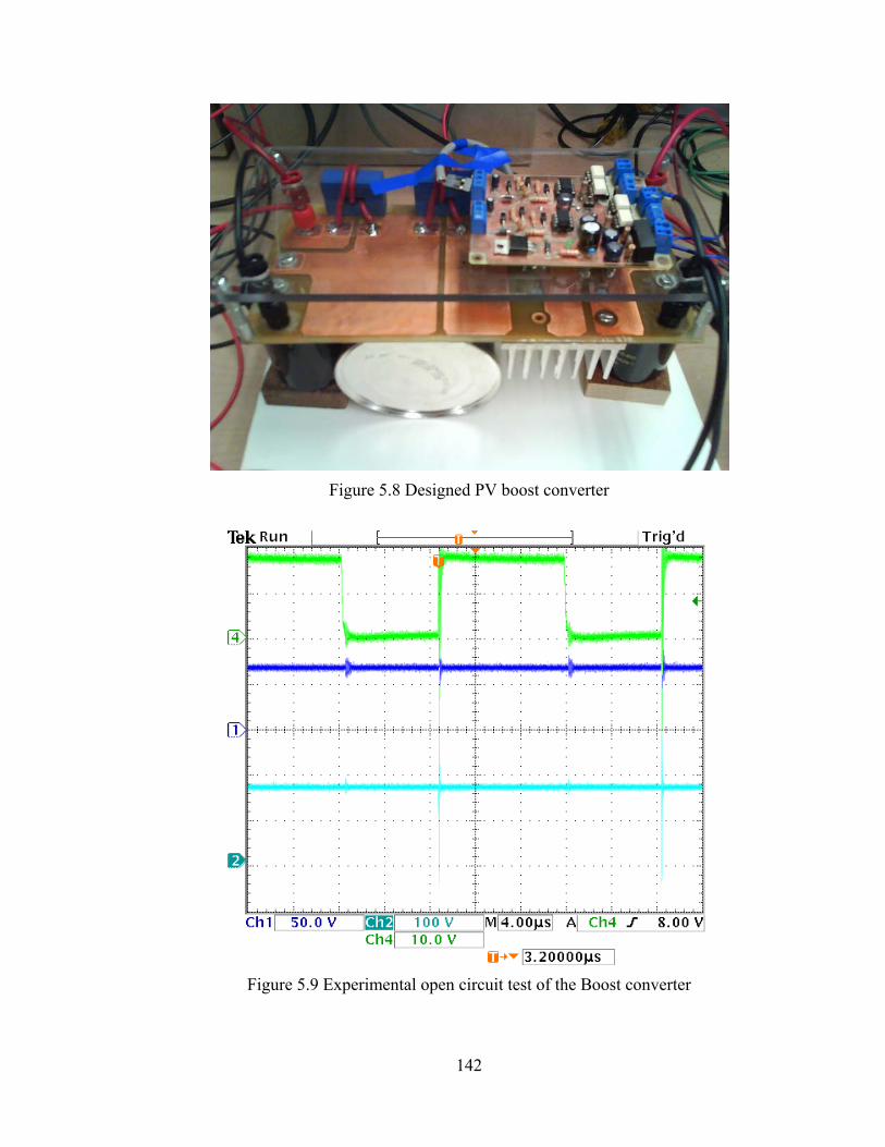
142
Figure 5.8 Designed PV boost converter
Figure 5.9 Experimental open circuit test of the Boost converter

143
built to connect the PV source to the resistive load. The ezDSPF28335 is used to control
the closed loop system.
The system under study is shown in Figure 5.1. It includes a programmable DC
power supply which is programmed to behave like a PV system. A DC/DC boost
converter is designed to connect the PV source to the resistive load. The process of the
design and open loop test of the boost converter is explained in previous section. . It is
considered as a 3kw DC/DC converter which works at the switching frequency of 50kHz
including input and output capacitors, a diode, a MOSFET as a switch and one high
frequency inductor. Rated output voltage of the input and output sides are designed to be
300V.
5.3.1 Design of the Current and Voltage Sensors
For closed loop tests we need to measure the output power of the PV system. For
this reason the voltage and current sensor circuits are designed. The output power is
calculated from the measured voltage and current. For the current sensor the LEM50P is
selected since its rating is up to 50 A. To increase the accuracy in lower currents two
turns of wires are wound around it. It then produces the same output voltage in the lower
(half) current magnitude. The current sensor is already mounted in series with the power
circuit board.
An interface circuit is designed to supply an isolated power to the sensor as well
as calibrate and filter the output. The designed PCB board of current sensor is presented
in Figure 5.10.

144
Figure 5.10 Designed PCB board for current sensor
Figure 5.11 Designed PCB board for voltage sensor

145
Figure 5.12 Designed PCB board for driver of the MOSFET
For a voltage sensor, the LV20P is used. The designed circuit is shown in Figure
5.11. It needs a ±12V to ±15V voltage supply. Based on the selected input and output
resistance of the sensor, the output voltage range for importing to the control part (DSP)
is zero to 3V for the actual input voltage of zero to 360V linearly.
5.3.2 Design of the Driver Circuit
One of the challenging parts for designing any converter is the driver circuit
especially if we want to operate in high frequencies. In DC/DC converters to reduce the
size of inductor, the switching frequency of the MOSFET is in a range of 10kHz to
100kHz. So a fast Driver with the least time delay, rise time, and fall time should be
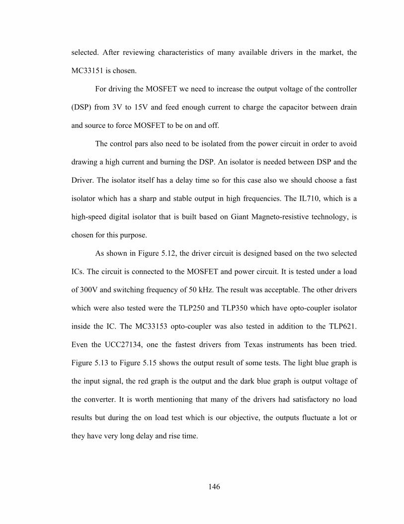
146
selected. After reviewing characteristics of many available drivers in the market, the
MC33151 is chosen.
For driving the MOSFET we need to increase the output voltage of the controller
(DSP) from 3V to 15V and feed enough current to charge the capacitor between drain
and source to force MOSFET to be on and off.
The control pars also need to be isolated from the power circuit in order to avoid
drawing a high current and burning the DSP. An isolator is needed between DSP and the
Driver. The isolator itself has a delay time so for this case also we should choose a fast
isolator which has a sharp and stable output in high frequencies. The IL710, which is a
high-speed digital isolator that is built based on Giant Magneto-resistive technology, is
chosen for this purpose.
As shown in Figure 5.12, the driver circuit is designed based on the two selected
ICs. The circuit is connected to the MOSFET and power circuit. It is tested under a load
of 300V and switching frequency of 50 kHz. The result was acceptable. The other drivers
which were also tested were the TLP250 and TLP350 which have opto-coupler isolator
inside the IC. The MC33153 opto-coupler was also tested in addition to the TLP621.
Even the UCC27134, one the fastest drivers from Texas instruments has been tried.
Figure 5.13 to Figure 5.15 shows the output result of some tests. The light blue graph is
the input signal, the red graph is the output and the dark blue graph is output voltage of
the converter. It is worth mentioning that many of the drivers had satisfactory no load
results but during the on load test which is our objective, the outputs fluctuate a lot or
they have very long delay and rise time.
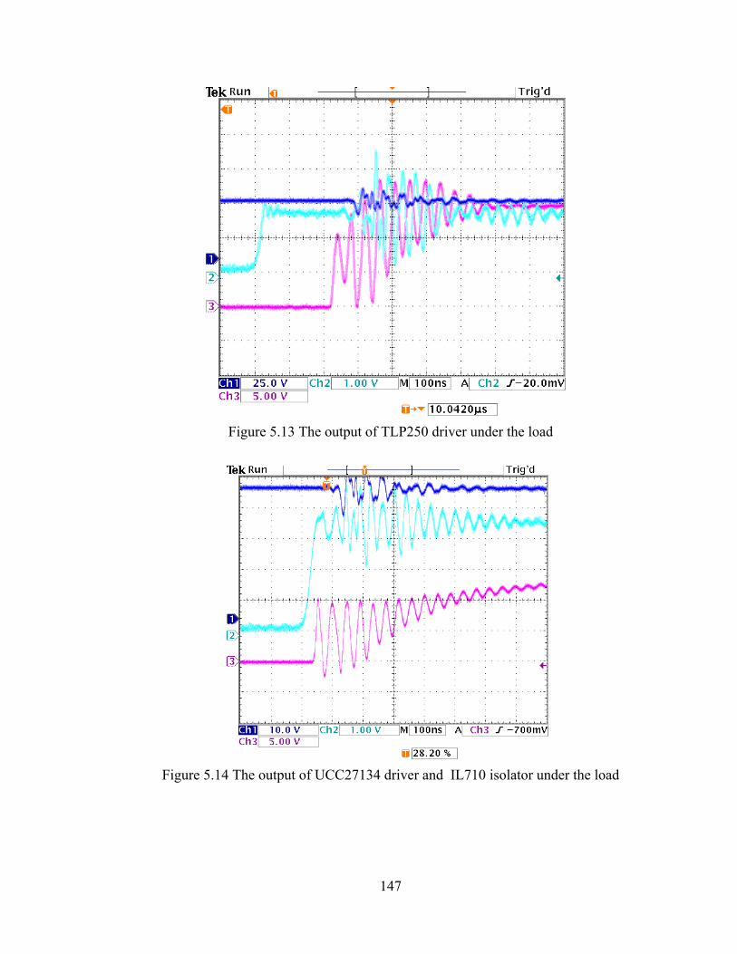
147
Figure 5.13 The output of TLP250 driver under the load
Figure 5.14 The output of UCC27134 driver and IL710 isolator under the load

148
After comparing all the results, the selected driver and isolator (MC33151 beside
IL710) had the best results from the delay, rising time, falling time and fluctuation during
turning on and off points of view.
5.3.3 Design of the Power Supply
All the designed boards including current and voltage sensors and the driver
circuit need a 24V input source. For this reason another PCB board is designed. This
board uses an AC 20VA, 115/48V transformer. The output of transformer is rectified,
filtered and regulated to DC 24V as the output. Figure 5.16 shows the designed power
supply circuit.
5.3.4 Controller Design and Closed Loop Test
The perturbation and observation (P&O) is selected for maximum power point
tracking of the PV system. In this type of controller, choosing the perturbation step size
which ensures a good matching between the tracking speed and the system dynamics is
very important. Choosing a big step causes power and voltage oscillation around MPP in
the steady-state while very small step size makes the controller dynamic slow. Therefore,
the characteristic of a general DC/DC boost converter in terms of step change of duty
ratio is studied. From the relationship between input and output voltage of the boost
converter in two different duty ratio with change of D

149
Figure 5.15 The output of MC33151 driver and IL710 isolator under the load
Figure 5.16 Designed PCB board for the power supply

150
D
VV in
o
11 (5.26)
)(12 DD
VV in
o
(5.27)
DDD
VVVV inooo 1
1
)(1
112
(5.28)
Thus we can define the relationship between amount of change of duty ratio and change
of output voltage in a special duty ratio if the input voltage is kept constant.
D
DV
VD
in
o
1
1
1
1
(5.29)
As it is shown in Figure 5.17, we can choose the desirable output voltage ripple of
the boost converter due to step change of duty ratio and define the duty ratio set point
(e.g., in maximum power point) and define the needed perturbation step size. Of course in
the P&O method, the lower the desirable voltage ripple, the slower controller dynamic.
For this purpose, 0.008 is selected for perturbation step size of the controller. The next
step is to study the steady state behavior of the whole system when we connect a
nonlinear PV system to a linear resistive load through a boost converter autonomously.
Figure 5.18 and Figure 5.19 show the characteristics of the programmed DC
source to behave like a PV panel. This characteristic is under rated irradiation level (i.e.
S=1). The experimental setup is based on this nonlinear PV characteristic. If the PV

151
0.00
5
0.00
5
0.005
0.005
0.01
0.01
0.01
0.01
0.01
5
0.015
0.015
0.015
0.02
0.02
0.02
0.02
0.02
5
0.025
0.025
0.03
0.03
0.03
0.03
5
0.035
0.035
0.04
0.04
0.04
0.045
0.045
0.045
0.05
0.05
0.05
0.055
0.055
0.055
0.06
0.06
0.06
0.065
0.065
0.07
0.07
0.075
0.075
0.08
0.08
0.085
0.085
0.09
0.09
0.095
0.095
0.1
0.1
0.105
0.105
0.11
0.11
0.115
0.120.125
0.130.135
0.140.145 0.15
(DeltaV/Vin)
D
DeltaD
0 0.01 0.02 0.03 0.04 0.05 0.06 0.07 0.08 0.09 0.1 0.11 0.12 0.13 0.14 0.15 0.16 0.17 0.18 0.19 0.20
0.05
0.1
0.15
0.2
0.25
0.3
0.35
0.4
0.45
0.5
0.55
0.6
0.65
0.7
0.75
0.8
0.85
0.9
0.95
0.99
Figure 5.17 Output voltage ripple of the boost converter in terms of change of duty ratio
in any predefine duty ratio set point
system is connected to the main grid with constant voltage which can absorb any power
from the PV, from the boost converter characteristic we will have
)1()1(1 DVDVVV gridopvin (5.30)
For increasing the output power of the PV we should increase the PV voltage, due to a
constant voltage at the output so the duty ratio should be reduced.
In the case of connecting the PV source to an autonomous constant resistive load,
the relationship between output voltage and current is linear and the relationship between
voltage and power is quadratic. To have power balance and also operate always in MPP
simultaneously, the output voltage can not be constant. From the power balance between

152
0 20 40 60 80 100 1200
0.5
1
1.5
2
2.5
X: 100.4Y: 1.793
Vpv (V)
Ipv
(A)
Figure 5.18 Programmed current versus voltage characteristic of experimental PV source
0 20 40 60 80 100 1200
20
40
60
80
100
120
140
160
180
200 X: 100.4Y: 180.1
Vpv (V)
Ppv
(W
)
Figure 5.19 Programmed output power versus voltage characteristic of experimental PV source
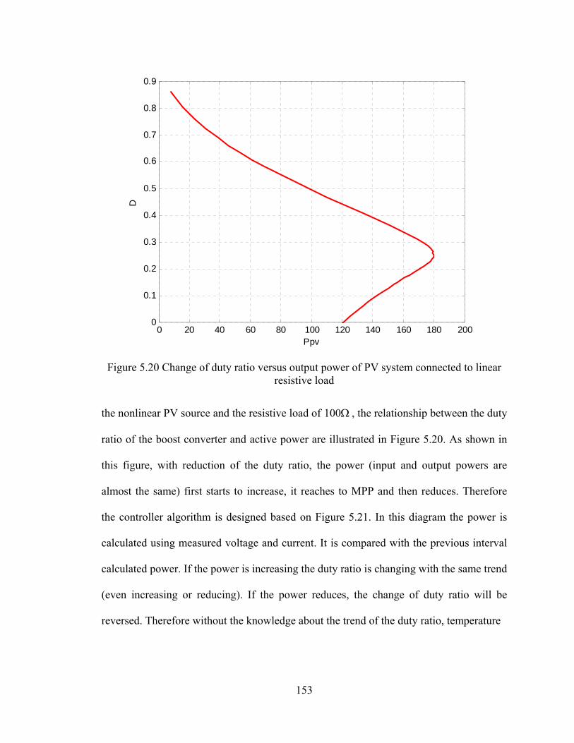
153
0 20 40 60 80 100 120 140 160 180 2000
0.1
0.2
0.3
0.4
0.5
0.6
0.7
0.8
0.9
Ppv
D
Figure 5.20 Change of duty ratio versus output power of PV system connected to linear resistive load
the nonlinear PV source and the resistive load of 100 , the relationship between the duty
ratio of the boost converter and active power are illustrated in Figure 5.20. As shown in
this figure, with reduction of the duty ratio, the power (input and output powers are
almost the same) first starts to increase, it reaches to MPP and then reduces. Therefore
the controller algorithm is designed based on Figure 5.21. In this diagram the power is
calculated using measured voltage and current. It is compared with the previous interval
calculated power. If the power is increasing the duty ratio is changing with the same trend
(even increasing or reducing). If the power reduces, the change of duty ratio will be
reversed. Therefore without the knowledge about the trend of the duty ratio, temperature

154
Measure Vpv(K), Ipv(K)
P(k)=Vpv(k)*Ipv(k)
P(k)>P(k-1)
DD
DkDkD )1()(
No
Yes
Figure 5.21 Schematic of the P&O algorithm for MPPT of the PV system
Table 5.2 Coefficients of the low pass Hamming digital filter
Coefficients
0a 1a 2a 3a 4a 5a 6a 7a 8a 9a
0.0161 0.0379 0.0931 0.1559 0.197 0.197 0.1559 0.0931 0.0379 0.0161
or even irradiation level the maximum power point of the PV can be obtained.
For measurement of the voltage and current, an RC low pass filter is first added to
the output of the sensors. Using coaxial cables the signals are transferred to the analog to
digital (A/D) converter pins of the DSP. Inside the program 12 bit digital values are
converter to floating point numbers and the measurements are calibrated to get the exact
value of the actual signals. An inside PWM with a frequency (sampling rate) of 100kHz
for the interrupt of A/D conversion is used. A 9th order Hamming digital low pass filter
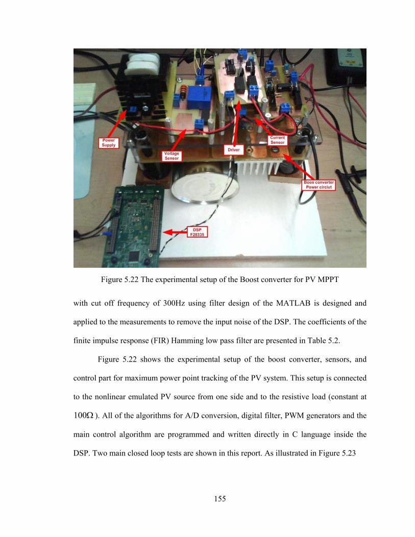
155
Figure 5.22 The experimental setup of the Boost converter for PV MPPT
with cut off frequency of 300Hz using filter design of the MATLAB is designed and
applied to the measurements to remove the input noise of the DSP. The coefficients of the
finite impulse response (FIR) Hamming low pass filter are presented in Table 5.2.
Figure 5.22 shows the experimental setup of the boost converter, sensors, and
control part for maximum power point tracking of the PV system. This setup is connected
to the nonlinear emulated PV source from one side and to the resistive load (constant at
100 ). All of the algorithms for A/D conversion, digital filter, PWM generators and the
main control algorithm are programmed and written directly in C language inside the
DSP. Two main closed loop tests are shown in this report. As illustrated in Figure 5.23

156
Figure 5.23 Experimental dynamic behavior of the load voltage of PV system using P&O MPP algorithm
Figure 5.24 Experimental steady state operation of the input power versus PV voltage in MPPT
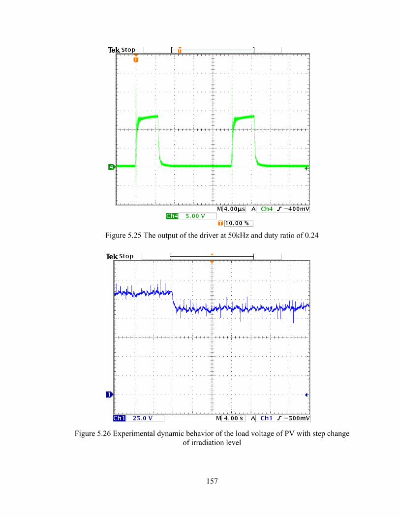
157
Figure 5.25 The output of the driver at 50kHz and duty ratio of 0.24
Figure 5.26 Experimental dynamic behavior of the load voltage of PV with step change of irradiation level

158
+
Figure 5.27 the bidirectional battery converter
the source is turned on from a zero set point at 30s. In this figure the dynamic response of
the controller for finding the maximum power point in a constant irradiation level (S=1)
is shown. After almost 20s the algorithm reaches the maximum power point which is
shown in Figure 5.24 . This is obtained from the online measurement of programmable
power source. After this moment it reaches steady state and has some small oscillations
in MPP. Figure 5.25 shows the output of the driver at a 50kHz switching frequency with
duty ratio of 0.24 which is the result of the PWM converter of the DSP controller
program obtaining maximum power point.
In second test the irradiation level is changed suddenly from unity to 0.8 at 12s.
As illustrated in Figure 5.26, the output voltage reaches the new steady state maximum
power set point in less than 4s. These two test show even with a sudden change of the
irradiation level of the sun, the perturbation and observation algorithm can find the
maximum power point of the PV in a few seconds.
5.4 Closed Loop Test of Battery System Converter
For charging and discharging of the battery, the same process as PV system is
followed to design the bidirectional buck and boost converter. As shown in Figure 5.27
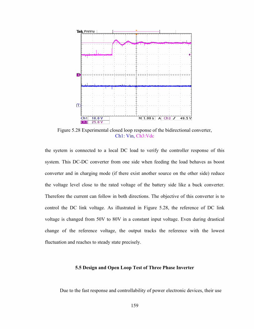
159
Figure 5.28 Experimental closed loop response of the bidirectional converter, Ch1: Vin, Ch3:Vdc
the syetem is connected to a local DC load to verify the controller response of this
system. This DC-DC converter from one side when feeding the load behaves as boost
converter and in charging mode (if there exist another source on the other side) reduce
the voltage level close to the rated voltage of the battery side like a buck converter.
Therefore the current can follow in both directions. The objective of this converter is to
control the DC link voltage. As illustrated in Figure 5.28, the reference of DC link
voltage is changed from 50V to 80V in a constant input voltage. Even during drastical
change of the reference voltage, the output tracks the reference with the lowest
fluctuation and reaches to steady state precisely.
5.5 Design and Open Loop Test of Three Phase Inverter
Due to the fast response and controllability of power electronic devices, their use

160
Figure 5.29 Three phase inverter simulated in MATLAB connected to the load
in electric power systems is growing fast. Most of the systems in the power system
network are working as three phase systems resulting three phase converters being the
most popular power electronic devices which are used in different topologies for a wide
variety of applications. Inverters can control the output voltage magnitude and frequency.
In this report the experimental setup for generating switching pulses using the sinusoidal
pulse width modulation (SPWM) in the three phase inverter is shown. The DSP F28335
is used for generating the pulses. The zero sequence is added to the modulation signal to
increase the linear modulation region. An interface circuit with isolators is designed to
connect the DSP to the gate drivers of the three phase inverter for experimental testing of
the system.
5.5.1 Study System
Figure 5.29 shows the study system which includes a three phase inverter
connected to a linear RL load through a capacitor filter and transmission line. This
161
system is modeled with MATLAB software. The switching pulses are applied from
imported DSP hardware. The model equations of the system are as follows:
The output voltage equations of inverter
nocpcffcffcpdc
nobpbffbffbpdc
noapaffaffapdc
vvpiLiRSv
vvpiLiRSv
vvpiLiRSv
122
122
122
(5.31)
where fR and fL are the resistance and inductance of the transmission line.
The load voltage equations
npcoocoocp
npbooboobp
npaooaooap
vpiLiRv
vpiLiRv
vpiLiRv
(5.32)
where oR and oL are the resistance and inductance of the linear RL load.
Capacitor voltage equations
cocfcpf
bobfbpf
aoafapf
iipvC
iipvC
iipvC
(5.33)
The fC is the capacitor capacitance.
The input current equation of the system is
cfcpbfbpafapdc iSiSiSi (5.34)
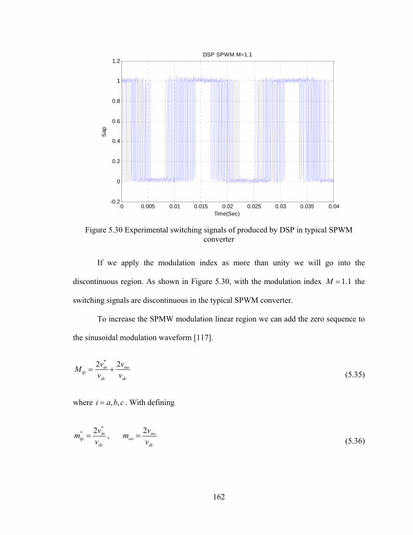
162
0 0.005 0.01 0.015 0.02 0.025 0.03 0.035 0.04-0.2
0
0.2
0.4
0.6
0.8
1
1.2
Time(Sec)
Sap
DSP SPWM M=1.1
Figure 5.30 Experimental switching signals of produced by DSP in typical SPWM converter
If we apply the modulation index as more than unity we will go into the
discontinuous region. As shown in Figure 5.30, with the modulation index 1.1M the
switching signals are discontinuous in the typical SPWM converter.
To increase the SPMW modulation linear region we can add the zero sequence to
the sinusoidal modulation waveform [117].
dc
no
dc
inip v
v
v
vM
22 *
(5.35)
where cbai ,, . With defining
dc
inip v
vm
** 2 ,
dc
nooo v
vm
2
(5.36)
163
ooipip mmM * (5.37)
and
maxmin 1212
vvv
v dcno
(5.38)
2
1
2
21
2
maxmin
dcdcdc
no
vv
vv
vv
(5.39)
maxmin 121 mmmoo (5.40)
Where dcv
vm min
min
2 , and
dcv
vm max
max
2
Therefore the actual modulation
maxmin* 121 mmmM ipip
(5.41)
where ***min ,,min cpbpap mmmm , ***
max ,,max cpbpap mmmm
The produced modulation waveform inside DSP is illustrated in Figure 5.31. The
produced switching signals of the modulation index are imported into MATLAB
software to be applied to the simulated system after adding the zero sequence waveform.
The produced output voltages of the simulated system are presented in Figure 5.32 with
no discontinuity in the waveform. The phase voltages of the capacitors are shown in
Figure 5.33 as three sinusoidal waveforms with 120 degree phase shifts.
The 6MBP50RA060 inverter module with the nominal 600V, 50A input voltage
and current ratings, consisting of six IGBTs and drivers is selected to convert the input

164
0 100 200 300 400 5000
0.1
0.2
0.3
0.4
0.5
0.6
0.7
0.8
0.9
1DSP M=1.1, =0.5
Ma
Mb
Mc
Figure 5.31 Modulation waveform after adding zero sequence to the typical SPWM in DSP
0.1 0.11 0.12 0.13 0.14 0.15 0.16 0.17-100
0
100
Vsa
Inverter Phase Voltage (DSP DPWM with =0.5 M=1.1)
0.1 0.11 0.12 0.13 0.14 0.15 0.16 0.17-100
0
100
Vsb
0.1 0.11 0.12 0.13 0.14 0.15 0.16 0.17-100
0
100
Vsc
Time(Sec)
Figure 5.32 Phase voltage of the inverter using imported DSP SPWM switching signals

165
0.1 0.11 0.12 0.13 0.14 0.15 0.16 0.17-60
-40
-20
0
20
40
60
Time(sec)
Vm
Capacitor Voltage (DSP DPWM with =0.5 M=1.1)
A
BC
Figure 5.33 Phase voltage of the simulated capacitor using imported DSP SPWM switching signals
Figure 5.34 Designed interface circuit to connect the DSP to the inverter drivers
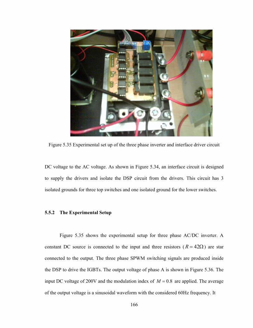
166
Figure 5.35 Experimental set up of the three phase inverter and interface driver circuit
DC voltage to the AC voltage. As shown in Figure 5.34, an interface circuit is designed
to supply the drivers and isolate the DSP circuit from the drivers. This circuit has 3
isolated grounds for three top switches and one isolated ground for the lower switches.
5.5.2 The Experimental Setup
Figure 5.35 shows the experimental setup for three phase AC/DC inverter. A
constant DC source is connected to the input and three resistors ( 42R ) are star
connected to the output. The three phase SPWM switching signals are produced inside
the DSP to drive the IGBTs. The output voltage of phase A is shown in Figure 5.36. The
input DC voltage of 200V and the modulation index of 8.0M are applied. The average
of the output voltage is a sinusoidal waveform with the considered 60Hz frequency. It

167
Figure 5.36 Experimental inverter output phase voltage of a resistive load with input DC voltage of 200V and modulation index M=0.8
Figure 5.37 Experimental inverter output phase voltage and phase current of a RL load with input DC voltage of 200V and modulation index M=0.8
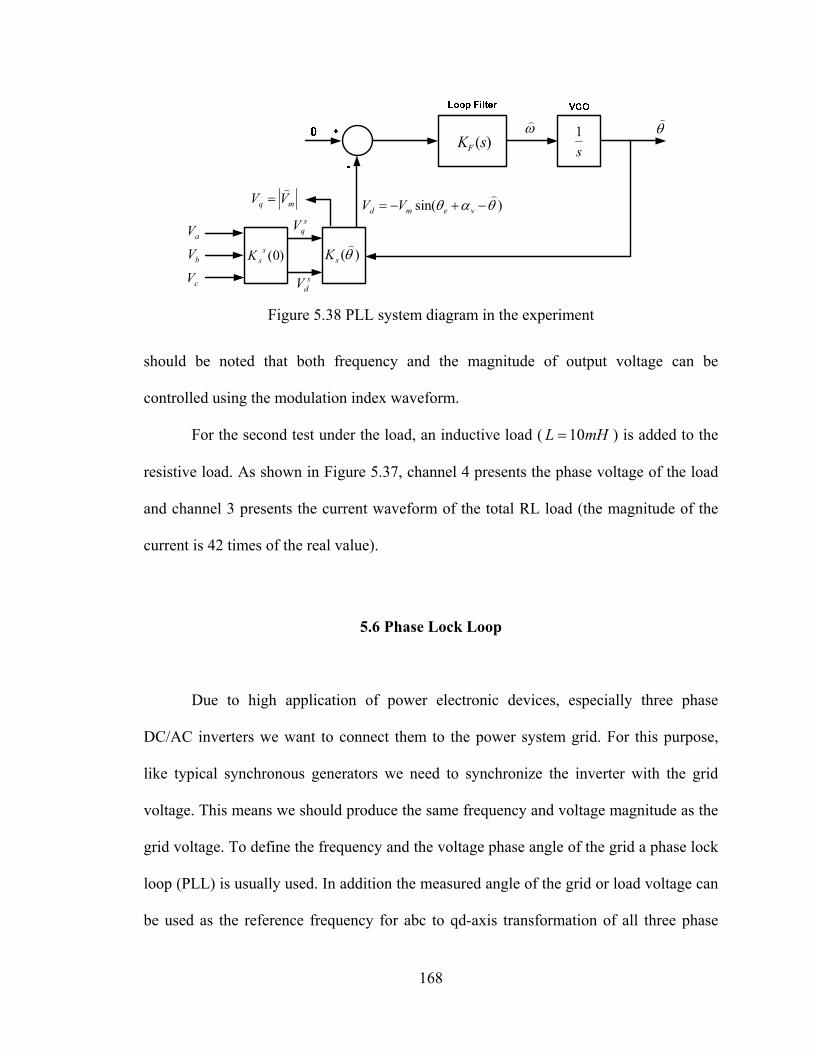
168
)(sKF s
1
aV
bV
cV
mq VV
s
qV
sdV
)(
sK )0(ssK
)sin(
vemd VV
Figure 5.38 PLL system diagram in the experiment
should be noted that both frequency and the magnitude of output voltage can be
controlled using the modulation index waveform.
For the second test under the load, an inductive load ( mHL 10 ) is added to the
resistive load. As shown in Figure 5.37, channel 4 presents the phase voltage of the load
and channel 3 presents the current waveform of the total RL load (the magnitude of the
current is 42 times of the real value).
5.6 Phase Lock Loop
Due to high application of power electronic devices, especially three phase
DC/AC inverters we want to connect them to the power system grid. For this purpose,
like typical synchronous generators we need to synchronize the inverter with the grid
voltage. This means we should produce the same frequency and voltage magnitude as the
grid voltage. To define the frequency and the voltage phase angle of the grid a phase lock
loop (PLL) is usually used. In addition the measured angle of the grid or load voltage can
be used as the reference frequency for abc to qd-axis transformation of all three phase

169
parameters. As it is shown in Figure 5.38 the three phase PLL uses measured local load
voltage and converts it to qd-axis frame then compares d-axis voltage with zero as a
reference. The error passes through a controller and then through a low pass filter to
remove noise. The idea of the PLL is to align the voltage to the q-axis and make the d-
axis voltage zero; therefore
)3
2cos(
)3
2cos(
)cos(
vemc
vemb
vema
VV
VV
VV
(5.42)
c
b
a
sd
q
f
f
f
K
f
f
f
0
,
2
1
2
1
2
1
)3
2sin()
3
2sin()sin(
)3
2cos()
3
2cos()cos(
3
2
sK , 0 t (5.43)
In stationary reference frame ( 0 )
2
3
2
30
2
1
2
11
3
2ssK
(5.44)
)(3
1
)22
(3
2
bcs
d
cba
sq
VVV
VVVV
(5.45)

170
bccbs
d
bcabcbbas
q
VVVV
VVVVVVV
3
1)(
3
13
1
3
2)(
3
1)(
3
2
(5.46)
Therefore instead of measuring phase voltages we can measure just two line to
line voltages. If transformation angle
, for transforming from stationary reference
frame to synchronous reference frame
cossin
sincos)(sK
cossin
sincoss
ds
qd
sd
sqq
VVV
VVV
(5.47)
)sin(
)cos(
vemd
vemq
VV
VV , 0
t
(5.48)
We assume (
ve )
sin
cos
md
mq
VV
VV
(5.49)
dt
d
dt
dxe
(5.50)
If 0dV 0sin 0 ve
The inverse qd transformation is
171
0
1
f
f
f
K
f
f
f
d
q
s
c
b
a
,
1)3
2sin()
3
2cos(
1)3
2sin()
3
2cos(
1)sin()cos(1
sK , 0 t (5.51)
cossin
sincos)(1
sK
cossin
sincos
dqs
d
dqs
q
VVV
VVV (5.52)
To define the abc reference frame voltages from the stationary reference frame values
2
3
2
12
3
2
1
01
1ssK
sd
sqc
sd
sqb
sqa
VVV
VVV
VV
2
3
2
1
2
3
2
1 (5.53)
The d-axis voltage equation is
)sin( siimimid VV (5.54)
If 0midV 0)sin( sii isi
)sin(0 siimimid VVe (5.55)
If )( sii is very small we can assume
)()sin( siisii (5.56)
siF
siimi s
sKV
)()(
(5.57)
Therefore one can define the closed loop transfer function and compare its denominator
with that of the second order standard Butterworth filter transfer function
172
)(
)(
sKVs
sKV
Fmi
Fmi
i
si
(5.58)
211
2
211
2 2
2
nn
nn
IpllmiPpllmi
IpllmiPpllmi
i
si
ss
s
kVksVs
kVksV
(5.59)
mi
nPpll V
k 12 and
mi
nIpll V
k21
(5.60)
where is the damping factor and is usually chosen as critical damping factor which is
707.0 and 1n is the natural frequency and it is chosen as )/(377 srad .
To examine the performance of the designed PLL, a three phase sinusoidal
voltage waveform is produced inside the DSP using the sine look up table. The output of
the PLL is stored inside the DSP and plotted in MATLAB. Figure 5.39 illustrates the
measured frequency and angle of the sample waveform from DSP. In Figure 5.40, the
original and the reproduced waveform from the measured frequency and angle of the
PLL are compared. This figure shows that the PLL precisely tracks the reference.
Figure 5.41 shows the transformed qd-axis of the voltage. Since the original
signal is purely sinusoidal, the q-axis voltage is exactly one per unit and d-axis voltage is
zero constantly.
5.7 Connection of Three Phase Inverter to the Grid
The main objective of the inverter in grid connected mode is to control the output
active and reactive power. The voltage magnitude and frequency is adopted from the
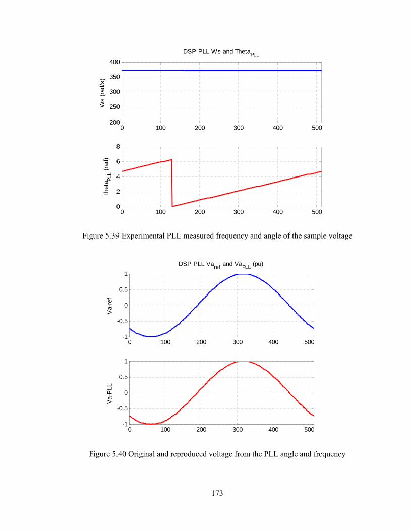
173
0 100 200 300 400 500200
250
300
350
400
Ws
(rad
/s)
DSP PLL Ws and ThetaPLL
0 100 200 300 400 5000
2
4
6
8
The
taPL
L (ra
d)
Figure 5.39 Experimental PLL measured frequency and angle of the sample voltage
0 100 200 300 400 500-1
-0.5
0
0.5
1
Va-
ref
DSP PLL Varef
and VaPLL
(pu)
0 100 200 300 400 500-1
-0.5
0
0.5
1
Va-
PLL
Figure 5.40 Original and reproduced voltage from the PLL angle and frequency
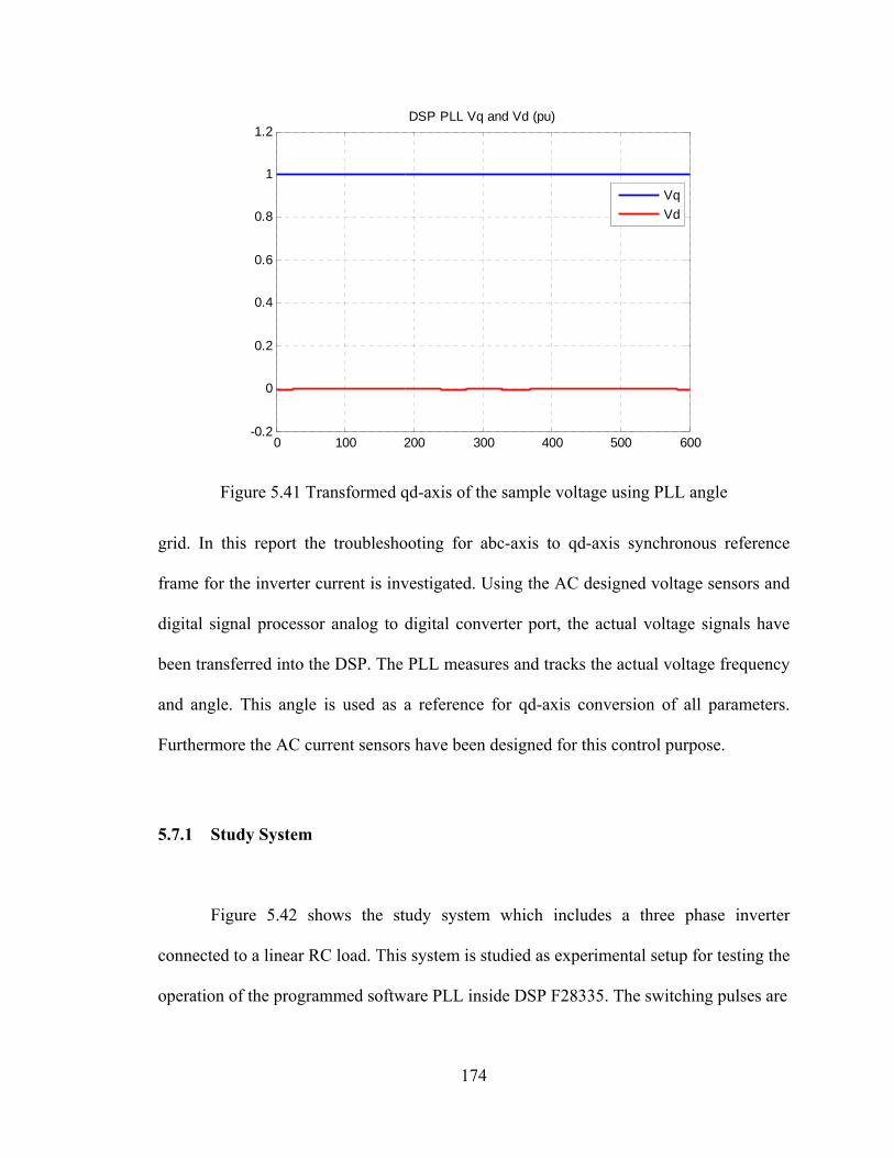
174
0 100 200 300 400 500 600-0.2
0
0.2
0.4
0.6
0.8
1
1.2DSP PLL Vq and Vd (pu)
Vq
Vd
Figure 5.41 Transformed qd-axis of the sample voltage using PLL angle
grid. In this report the troubleshooting for abc-axis to qd-axis synchronous reference
frame for the inverter current is investigated. Using the AC designed voltage sensors and
digital signal processor analog to digital converter port, the actual voltage signals have
been transferred into the DSP. The PLL measures and tracks the actual voltage frequency
and angle. This angle is used as a reference for qd-axis conversion of all parameters.
Furthermore the AC current sensors have been designed for this control purpose.
5.7.1 Study System
Figure 5.42 shows the study system which includes a three phase inverter
connected to a linear RC load. This system is studied as experimental setup for testing the
operation of the programmed software PLL inside DSP F28335. The switching pulses are

175
gaV
gbV
gcV
gR gL1sR 1sL
asI 1 gaI
1sC
amV 1
LR
Figure 5.42 Three phase inverter connected to the grid and resistive load.
Table 5.3 The study system parameters
dcV 100 V 1sC F30
1sR 15.0 1sL mH10
LR 42 gV V3
220
applied from DSP hardware. Table 5.3 shows the parameters of the system. The model
equations of the system are as follows: The output voltage equations of inverter
nocmcsscsscpdc
nobmbssbssbpdc
noamassassapdc
VVpILIRSV
VVpILIRSV
VVpILIRSV
11111
11111
11111
122
122
122
(5.61)
where 1sR , 1sL and abcmV 1 are resistance, inductance of the filter and phase voltage of the
capacitor.

176
Capacitor voltage equations
gcL
cmcscms
gbL
bmbsbms
gaL
amasams
IR
VIpVC
IR
VIpVC
IR
VIpVC
1111
1111
1111
(5.62)
The grid equations are
gccmgcggcg
gbbmgbggbg
gaamgaggag
VVpILIR
VVpILIR
VVpILIR
1
1
1
(5.63)
The input current equation of the system is
cscpbsbpasapdc ISISISI 111 (5.64)
In Figure 5.43 the single line diagram of the three phase inverter during the
connection to the grid is shown. An AC voltage sensor is designed to measure and send
the sensed line to line voltages ( 1mV ) to the digital signal processor (DSP) unit.
Figure 5.44 illustrates the structure of PCB board for the designed AC voltage
sensor. Because the analog to digital converter of the DSP just accepts the positive
voltages, the output of the voltage sensor which is between -1.5V to 1.5V should be
increased to be between 0 to 3V. For this purpose a precise 1.5V DC offset is produced
using a programmable shunt regulator (LM431). An opamp added this offset to the output
of the voltage sensor. Therefore the input AC voltage magnitude of 0 to 250V is
converted to 0 to 1.5V in the output of the voltage sensor.

177
LR
2dc
a
VM 1mV
2mV gaVgR gL
1sL1sR
asI 1
1sC
1S
Figure 5.43 Single line diagram of the study system in connection to the grid.
Figure 5.44 Designed PCB board for AC voltage sensor.
The measured frequency of the grid using a PLL is shown in Figure 5.45. In
addition the transformed voltage of the grid to qd-axis format using the measures PLL
angle and frequency is illustrated in Figure 5.46.
After defining the frequency and phase angle of the grid voltage, a DC voltage is applied
to the input of the three phase inverter and the output voltage of the inverter is produced
based on that angle and frequency. The RLC filter attenuates the high switching
frequency ripples of the voltage and getting a sinusoidal waveform in the output of

178
0 0.01 0.02 0.03 0.04 0.05 0.06360
365
370
375
380
385
390
time (s)
Ws
(rad
/s)
0 0.01 0.02 0.03 0.04 0.05 0.06-5
0
5
10
15
20
25
30
35
time (s)
Vm
qd (
V)
Vmq
Vmd
Figure 5.45 The measure angular frequency of the grid using PLL
Figure 5.46 The measured line to line grid voltage transformed to qd-axis
inverter at the point of common coupling (PCC). To make two voltages of 1mV and 2mV
on the two sides of the connection switch as close as possible in both magnitude and
phase angle, the effect of filter is also included in calculation of inverter modulation
indices. In qd-axis format
dsqssdmdc
d
qsdssqmdc
q
IRILVV
M
IRILVV
M
111111
111111
2
2
(5.65)
We need to measure the current of the RL filter. A three phase AC current sensor
is designed. Figure 5.47 shows the schematic of an AC current sensor with a 1.5V DC
offset to produce positive output all of the time in the range of zero to 25 A input AC
current. The designed PCB board of the three phase current sensor is shown in Figure
5.48.
In Figure 5.49 the voltage on both sides of the switch ( 1S ) are presented. As
presented in Figure 5.49 using measured currents and voltages and (5.65). There is still a

179
iI
iI
Figure 5.47 Schematic diagram of AC current sensor
slight difference between the voltage magnitude and phase angle in both sides of the
connection switch at PCC. Besides the inaccurate values of the system parameters and
tolerance in measurements two main issues are investigated. The first one is the delay due
to sensors and especially the digital filter inside the DSP which affects the phase angle.
The second one is the effect of dead-time applied to IGBT switches which is discussed as
follows.
To avoid the short circuit in one leg and switch at zero voltage to reduce
switching losses, the dead-time should be applied to power electronic switches. In Figure
5.50 the output voltage in a constant switching frequency and different modulation index
and DC-link voltage is illustrated. The only difference of Figure 5.50(a) and (c) is the
applied dead time. It can be seen that in the second case with dead time the output voltage
is less. In Figure 5.50(b) and (d) half of the previous modulation index is applied to get
the same voltage and (theoretically) the DC-link voltage is doubled. As it happens in the
simulation, Figure 5.50(a) and (b) have the same output but Figure 5.50(d) with even
with the same dead-time has less output from Figure 5.50(d). As a result, applying dead-
time, not only reduces the output voltage magnitude but also result in higher DC-link

180
Figure 5.48 PCB board of three AC current sensors.
Figure 5.49 Experimental measured voltages on two sides of the switch before connection. ( Ch1: Vm1 Ch4:Vm2 Ch3:Is1c)
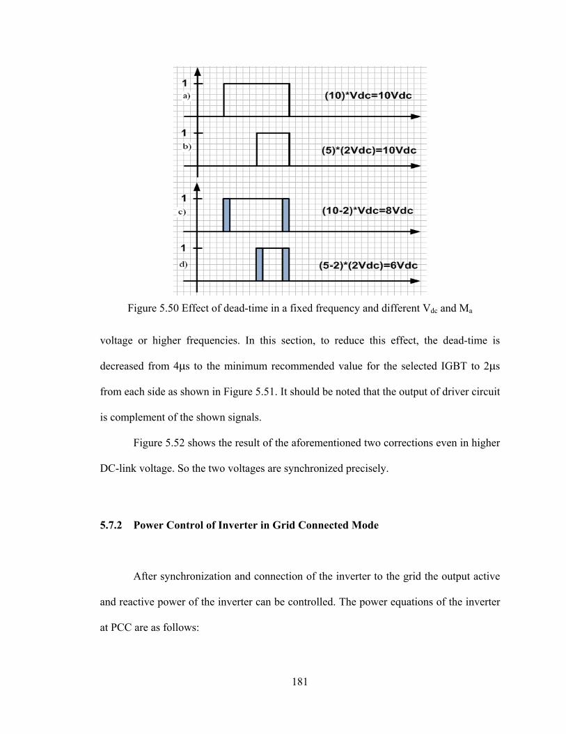
181
Figure 5.50 Effect of dead-time in a fixed frequency and different Vdc and Ma
voltage or higher frequencies. In this section, to reduce this effect, the dead-time is
decreased from 4μs to the minimum recommended value for the selected IGBT to 2μs
from each side as shown in Figure 5.51. It should be noted that the output of driver circuit
is complement of the shown signals.
Figure 5.52 shows the result of the aforementioned two corrections even in higher
DC-link voltage. So the two voltages are synchronized precisely.
5.7.2 Power Control of Inverter in Grid Connected Mode
After synchronization and connection of the inverter to the grid the output active
and reactive power of the inverter can be controlled. The power equations of the inverter
at PCC are as follows:
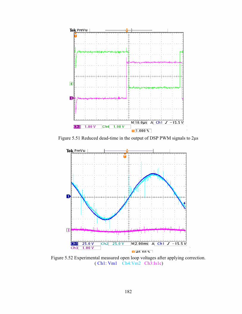
182
Figure 5.51 Reduced dead-time in the output of DSP PWM signals to 2μs
Figure 5.52 Experimental measured open loop voltages after applying correction. ( Ch1: Vm1 Ch4:Vm2 Ch3:Is1c)

183
))(2
3(
))(2
3(
11111
11111
qsdmdsqms
dsdmqsqms
IVIVQ
IVIVP
(5.66)
In grid connected mode the qd-axis of the voltage is known and adopted from the
grid therefore we can define the current references from the output power references and
measured qd-axis voltages.
21
21
11*1
21
21
11*1
dmqm
qmrefdmrefds
dmqm
dmrefqmrefqs
VV
VQVPI
VV
VQVPI
(5.67)
To design the current controller, from the dynamic equation of the system
dsdsdsdsqsssdmdcd
dssdss
qsqsqsqsdsssqmdcq
qssqss
IIskILVVM
IRIsL
IIskILVVM
IRIsL
11*
1111111
1111
11*
1111111
1111
))((2
))((2
(5.68)
Applying the PI controller, the current controllers transfer functions are
)(1
1
1
1
)(
)(
1
111111
1
*1
1
sk
RsLsskRsL
sk
I
I
qs
sssqsss
qs
qs
qs
(5.69)
)(1
1
1
1
)(
)(
1
111111
1*
1
1
sk
RsLsskRsL
sk
I
I
ds
sssdsss
ds
ds
ds
(5.70)
where

184
refP
refQ
*1qsI
qsI 1
*1dsI
dsI 1
qs1
ds1s
kk Is
Ps1
1
11 ssL
1
2
dcV
1qM
1dM
1
2
dcV
dmV 1
qmV 1
s
kk Is
Ps1
1
11 ssL
21
21
11*1
21
21
11*1
dmqm
qmrefdmrefds
dmqm
dmrefqmrefqs
VV
VQVPI
VV
VQVPI
Figure 5.53 Inverter current control structure
s
kk
s
RsLsksk Is
Pss
ssqsqs
11
1
1111 )()(
(5.71)
So we can calculate the coefficients of PI current controller as
47.942
68.81
1
11
1
11
s
sIs
s
sPs
Rk
Lk
(5.72)
where for fast response the time constant is chosen to be five times of switching
frequency time intervals
sws f
2
151
(5.73)
The modulation indices which are the outputs of the controllers are given as
)(2
)(2
111111
1
111111
1
qsssdmdsdc
d
dsssqmqsdc
q
ILVV
M
ILVV
M
(5.74)

185
The closed loop current and power control of the system is illustrated in Figure
5.53. After applying the controller inside DSP, Figure 5.54 shows the line to line voltage
at PCC after connection and the phase current when the active power is set to 50W and
reactive power is set to 5 Var.
In Figure 5.55, the values of active and reactive power references are changed to
100W and 10Var respectively. As it is shown, when the power output reference has been
doubled the value of current magnitude drawn from the inverter is two times of the
previous case. To show the dynamic response of the controller, 600 samples at the
moment of power change is stored inside DSP. In Figure 5.56, the controller follows the
reference active and reactive power in a very short transient. Due to the small amount of
reactive power the transients are more significant.
Since the inverter and the whole setup is designed for higher voltage and power,
the experiment is repeated in higher DC-link and grid voltages. The presented active and
reactive powers in Figure 5.57 at higher voltage have more fluctuations. The amount of
fluctuations in higher power isn’t acceptable and makes the controller to fail tracking the
references.
For solving the problem, the output of current sensors, inside the DSP after
passing a low pass digital filter are studied. Therefore, in the first attempt the current
sensors of the three phase have been calibrated. Even after calibration, the same problem
occurred. Thus in the next step, the saved data was synthesized and transformed inside
MATLAB software to be sure about the qd-axis transformation. Getting the same result
as the experiment encouraged the study of the output line to line voltage data of the
inverter from the oscilloscope inside MATLAB.

186
Figure 5.54 The experimental grid voltage (Ch1) and inverter output phase current (Ch3), VarQWP refref 5,50
Figure 5.55 The experimental grid voltage (Ch1) and inverter output phase current (Ch3), VarQWP refref 10,100
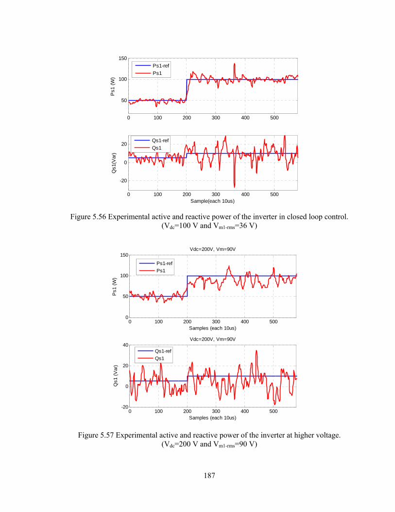
187
0 100 200 300 400 500
50
100
150
Ps1
(W
)
Ps1-ref
Ps1
0 100 200 300 400 500
-20
0
20
Sample(each 10us)
Qs1
(Var
)
Qs1-ref
Qs1
Figure 5.56 Experimental active and reactive power of the inverter in closed loop control. (Vdc=100 V and Vm1-rms=36 V)
0 100 200 300 400 5000
50
100
150
Ps1
(W
)
Samples (each 10us)
Vdc=200V, Vm=90V
Ps1-ref
Ps1
0 100 200 300 400 500-20
0
20
40
Qs1
(V
ar)
Samples (each 10us)
Vdc=200V, Vm=90V
Qs1-ref
Qs1
Figure 5.57 Experimental active and reactive power of the inverter at higher voltage. (Vdc=200 V and Vm1-rms=90 V)

188
Figure 5.58 shows that this waveform has a fifth harmonic. To reduce the
harmonic, the switching frequency of the inverter from asynchronous 5kHz is changed to
synchronous 4860Hz (81*60) which is a multiply of three times the modulation signal
(grid) frequency (60Hz). The result is presented in Figure 5.59 which shows fewer
harmonics inside the voltage. Actually, harmonics in the second graph are spread around
the switching frequency which can be removed with small low pass filters. The DC
harmonics in the both last graphs are due to DC offset in the differential probes of
oscilloscope.
5.8 Comparison of PLL and EPLL
In most power system applications the current and voltage magnitudes and angle
should be measured and controlled. Those parameters are needed even to control the
active and reactive power or the torque in the electrical machine.
Phase lock loop (PLL) has been used widely to define the frequency and the angle
of the voltage either in single phase or three phase systems. This angle is used as a
reference to convert the three phase parameters from abc reference frame to qd-axis
synchronous reference frame. In qd-axis synchronous reference frame the parameters are
DC quantities so the linear controllers can be applied to them.
One of the challenges for converting the parameters to qd-axis reference frame is
the noise. Therefore, the output measured signals can not be constant as we expect in the
experiment.
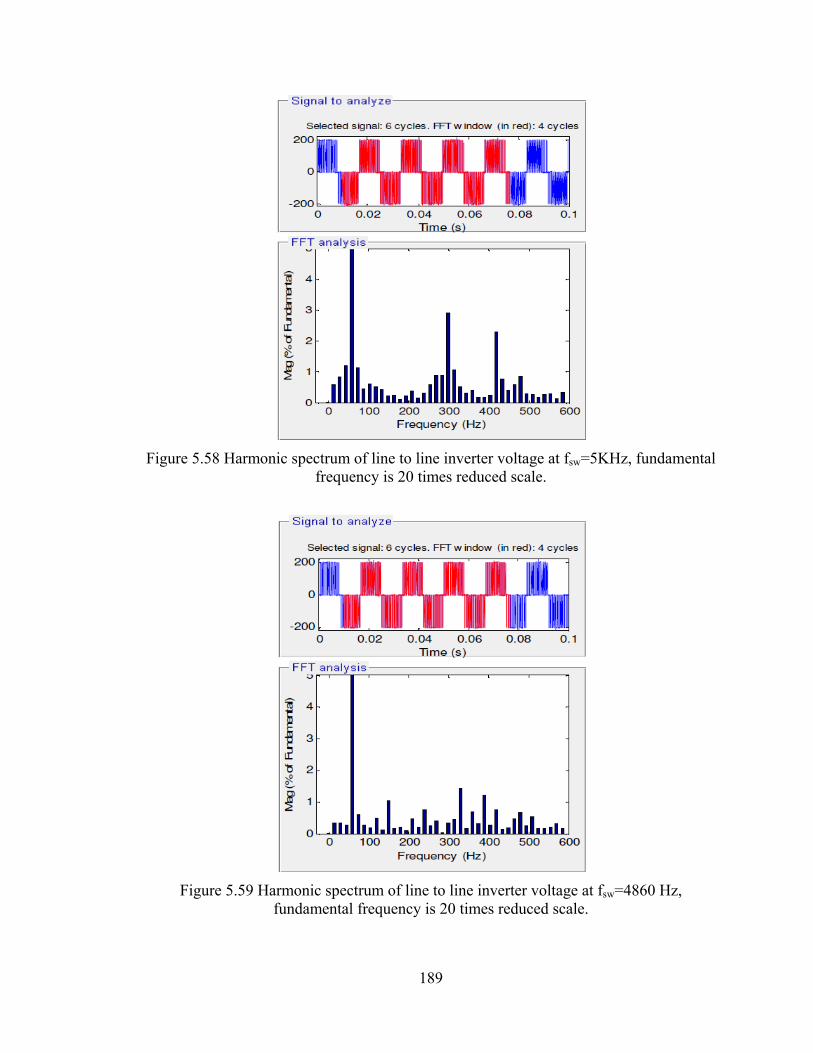
189
Figure 5.58 Harmonic spectrum of line to line inverter voltage at fsw=5KHz, fundamental frequency is 20 times reduced scale.
Figure 5.59 Harmonic spectrum of line to line inverter voltage at fsw=4860 Hz, fundamental frequency is 20 times reduced scale.
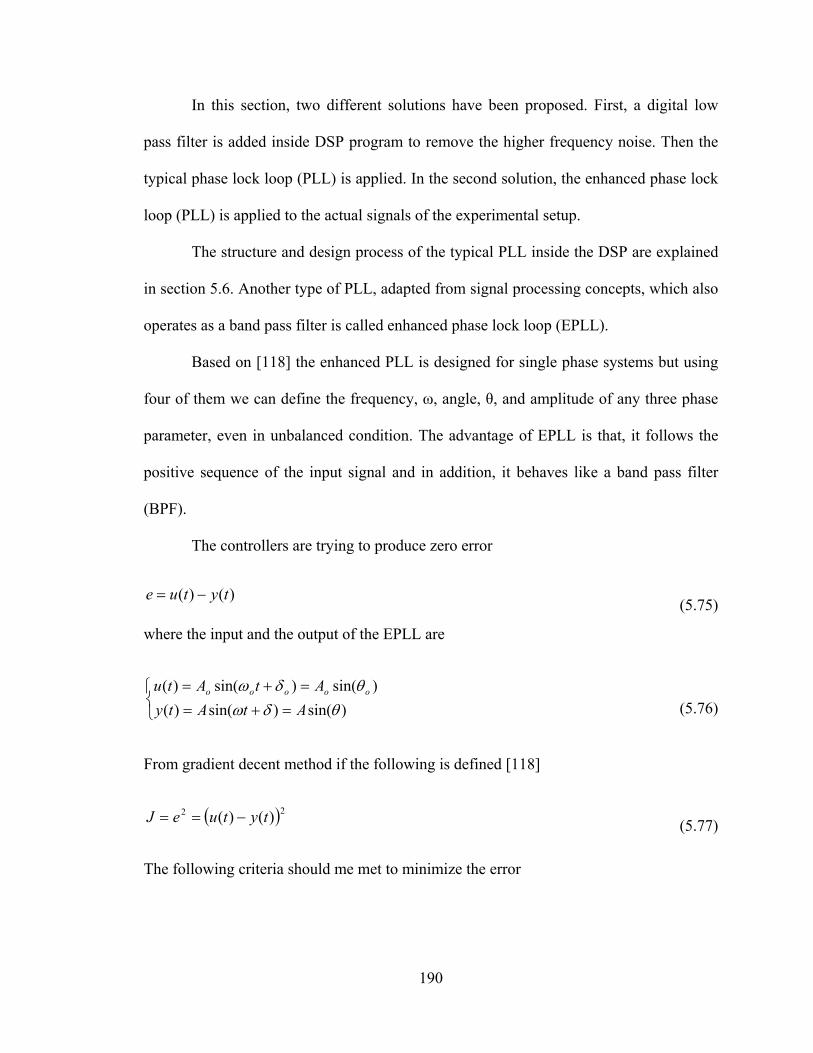
190
In this section, two different solutions have been proposed. First, a digital low
pass filter is added inside DSP program to remove the higher frequency noise. Then the
typical phase lock loop (PLL) is applied. In the second solution, the enhanced phase lock
loop (PLL) is applied to the actual signals of the experimental setup.
The structure and design process of the typical PLL inside the DSP are explained
in section 5.6. Another type of PLL, adapted from signal processing concepts, which also
operates as a band pass filter is called enhanced phase lock loop (EPLL).
Based on [118] the enhanced PLL is designed for single phase systems but using
four of them we can define the frequency, ω, angle, θ, and amplitude of any three phase
parameter, even in unbalanced condition. The advantage of EPLL is that, it follows the
positive sequence of the input signal and in addition, it behaves like a band pass filter
(BPF).
The controllers are trying to produce zero error
)()( tytue (5.75)
where the input and the output of the EPLL are
)sin()sin()(
)sin()sin()(
AtAty
AtAtu ooooo (5.76)
From gradient decent method if the following is defined [118]
22 )()( tytueJ (5.77)
The following criteria should me met to minimize the error

191
pdpp
Jp
A
JpA
o
t
3131
21
11
)(
)(
)(
(5.78)
oAep
Aep
epA
)cos(
)cos(
)sin(
3121
21
11
(5.79)
To design the controller parameters of EPLL from the dynamic equations of the
amplitude controller
)sin()sin()sin()sin( 1111 AAepA oo (5.80)
If we consider the angle control has already reached the reference
AAAApA ooo )2cos(221111
(5.81)
Therefore the linear approximation of the amplitude controller yields to
2
211
11
1
pA
AH
o
(5.82)
To design the phase and frequency controllers, if we consider the amplitude
control has already reached the reference, from their dynamic equations
)sin()sin()cos(
)sin()sin()cos(
31212
212
oo
o
Ap
Ap (5.83)

192
)2sin()sin()sin(2
)2sin()sin()sin(2
31212
212
ooo
oo
Ap
Ap
(5.84)
Due to the closed loop control, the estimated and actual angles are very close thus
)()sin( oo , in addition from the linear approximation of the above equation
ooA
A
A
A
p
p
0
2
2
21
20
31212
212
31212
212
(5.85)
The characteristic equation is
21
2212
13121
22
111 222 ooS
AAAI (5.86)
Therefore two of the parameters of the EPLL can be defined as
2121
31
2
2
21
4
2
A
A
o
o
(5.87)
In a general case for a three phase system when the three phases are unbalanced
)sin(
)sin(
)sin(
11
11
11
cccc
bbbb
aaaa
epA
epA
epA
(5.88)

193
)cos(
)cos(
)cos(
21
21
21
ccccc
bbbbb
aaaaa
eAp
eAp
eAp
(5.89)
occcccccc
obbbbbbbb
oaaaaaaaa
eAp
eAp
eAp
)cos(
)cos(
)cos(
3121
3121
3121
(5.90)
The designed parameters for the unbalanced three phase system
2
2
2
2
2
2
2
2
2
2
2
2
c
oc
b
ob
a
oa
A
A
A
(5.91)
cc
oc
bb
ob
aa
oa
A
A
A
2121
3
2121
3
2121
3
4
4
4
(5.92)
From (5.91) and (5.92), for the unbalanced three phase system first of all the
frequency and angle controller parameters are coupled and seconly related to the
magnitude of each phase. So in an unbalanced system different controllers should be
applied. To solve this problem if the structure of the controller is changed and the
dynamic equations of the EPLL are rewrittien as follows:

194
oA
ep
A
ep
epA
)cos(
)cos(
)sin(
3
2
1
and
31212
3
212
2
111
A
A (5.93)
From (5.93) the redesigned structure of the EPLL for a single phase system is shown in
Figure 5.60. It has three parameter controllers. The control of amplitude is almost
independent of the phase angle and frequency control. To design the controller
parameters of EPLL from the dynamic equations of the amplitude controller
)sin()sin()sin()sin( 11 AAepA oo (5.94)
If we consider the angle control has already reached the reference
AAAApA ooo )2cos(22
11
(5.95)
Therefore the linear approximation of the amplitude controller yields to
2
21
1
1
pA
AH
o
(5.96)
To design the phase and frequency controllers, if we consider the amplitude
control has already reached the reference, from their dynamic equations
)sin()sin()cos(
)sin()sin()cos(
3
2
oo
o
p
p (5.97)
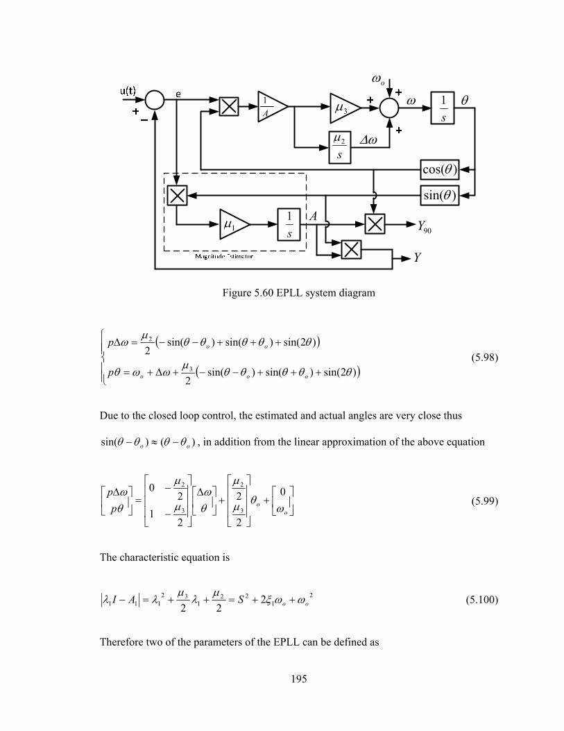
195
s2
s
1
)sin(
)cos(
1 s
1
3
o
A90Y
Y
A
1
Figure 5.60 EPLL system diagram
)2sin()sin()sin(2
)2sin()sin()sin(2
3
2
ooo
oo
p
p (5.98)
Due to the closed loop control, the estimated and actual angles are very close thus
)()sin( oo , in addition from the linear approximation of the above equation
oop
p
0
2
2
21
20
3
2
3
2
(5.99)
The characteristic equation is
21
221
32111 2
22 ooSAI
(5.100)
Therefore two of the parameters of the EPLL can be defined as

196
2
2
13 2
o
o
(5.101)
Threfore the controller parameters in the new structure are independent of the input
signal magnitude and the same designed parameters can be applied to the unbalanced
system.
If look at the whole system and define two new variables as
)cos(
)sin(
2
1
Ax
Ax (5.102)
31112
23
21121
)cos()sin(
)(cos)(sin
xuxpx
xuxpx
o
o (5.103)
These equations are nonlinear so if we consider 31 , it will be
2
1
1
2
11
2
1
01
00
x
xy
ux
x
px
px
o
o
(5.104)
Thus the transfer function is a second order band pass filter equation as follows:
22
2
22
12
1
2
2
oo
o
o ss
s
ss
s
y
u
(5.105)
The EPLL is originally designed for a single phase system. The algorithm to
define the angle, frequency and the amplitude of the three phase signal is illustrated in
Figure 5.61. It includes four single phase EPLLs and a compensator unit. The first three

197
Figure 5.61 EPLL structure for three phase system
EPLLs, act like band pass filters when they follow the input signals ( cba fff ,, ).
Therefore they remove the noises. The compensator extracts the positive sequence
( cba fff ,, ) of the three phase filtered signals. Another advantage of EPLL is that it
produces automatically both the filtered signal ( y ) and its 90 degree phase shifted one
( 90y ) which makes producing positive sequence easier.
120
2
2
2
,
1
1
1
3
1 j
c
b
a
c
b
a
e
V
V
V
V
V
V
(5.106)
Or
cab
babacc
cbcbaa
VVV
VVVVVV
VVVVVV
90_90_
90_90_
32
1
6
1
3
132
1
6
1
3
1
(5.107)
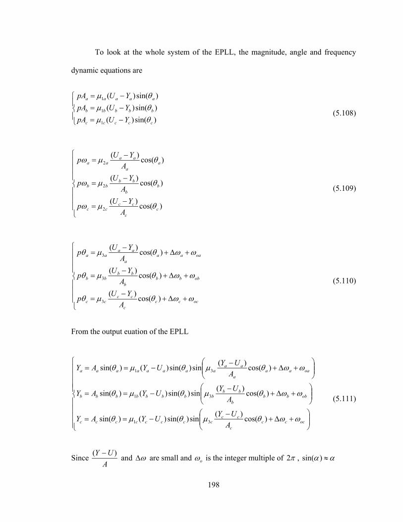
198
To look at the whole system of the EPLL, the magnitude, angle and frequency
dynamic equations are
)sin()(
)sin()(
)sin()(
1
1
1
ccccc
bbbbb
aaaaa
YUpA
YUpA
YUpA
(5.108)
)cos()(
)cos()(
)cos()(
2
2
2
cc
cccc
bb
bbbb
aa
aaaa
A
YUp
A
YUp
A
YUp
(5.109)
occcc
cccc
obbbb
bbbb
oaaaa
aaaa
A
YUp
A
YUp
A
YUp
)cos()(
)cos()(
)cos()(
3
3
3
(5.110)
From the output euation of the EPLL
occcc
cccccccccc
obbbb
bbbbbbbbbb
oaaaa
aaaaaaaaaa
A
UYUYAY
A
UYUYAY
A
UYUYAY
)cos()(
sin)sin()()sin(
)cos()(
sin)sin()()sin(
)cos()(
sin)sin()()sin(
31
31
31
(5.111)
Since A
UY )( and are small and o is the integer multiple of 2 , )sin(
199
occcc
cccccccc
obbbb
bbbbbbbb
oaaaa
aaaaaaaa
A
UYUYY
A
UYUYY
A
UYUYY
)cos()(
)sin()(
)cos()(
)sin()(
)cos()(
)sin()(
31
31
31
(5.112)
))(sin()(
)sin()cos(
))(sin()(
)sin()cos(
))(sin()(
)sin()cos(
1
2
31
1
2
31
1
2
31
ccccoccc
ccccccc
bbbbobbb
bbbbbbb
aaaaoaaa
aaaaaaa
UYA
UYY
UYA
UYY
UYA
UYY
(5.113)
Again when A
UY )( is small, taking the linear part
)sin(1
)sin(
)sin(1
)sin(
)sin(1
)sin(
1
1
1
1
1
1
ccocc
ccocc
c
c
bbobb
bbobb
b
b
aaoaa
aaoaa
a
a
U
Y
U
Y
U
Y
(5.114)
For the second input with 90 degree shift in the angle
)sin(
)cos()cos(
)sin(
)cos()cos(
)sin(
)cos(
)sin(
)cos()sin()cos(
90
90
90
c
ccccc
b
bbbbb
a
aa
a
aaaaaa
YAY
YAY
YAAY
(5.115)
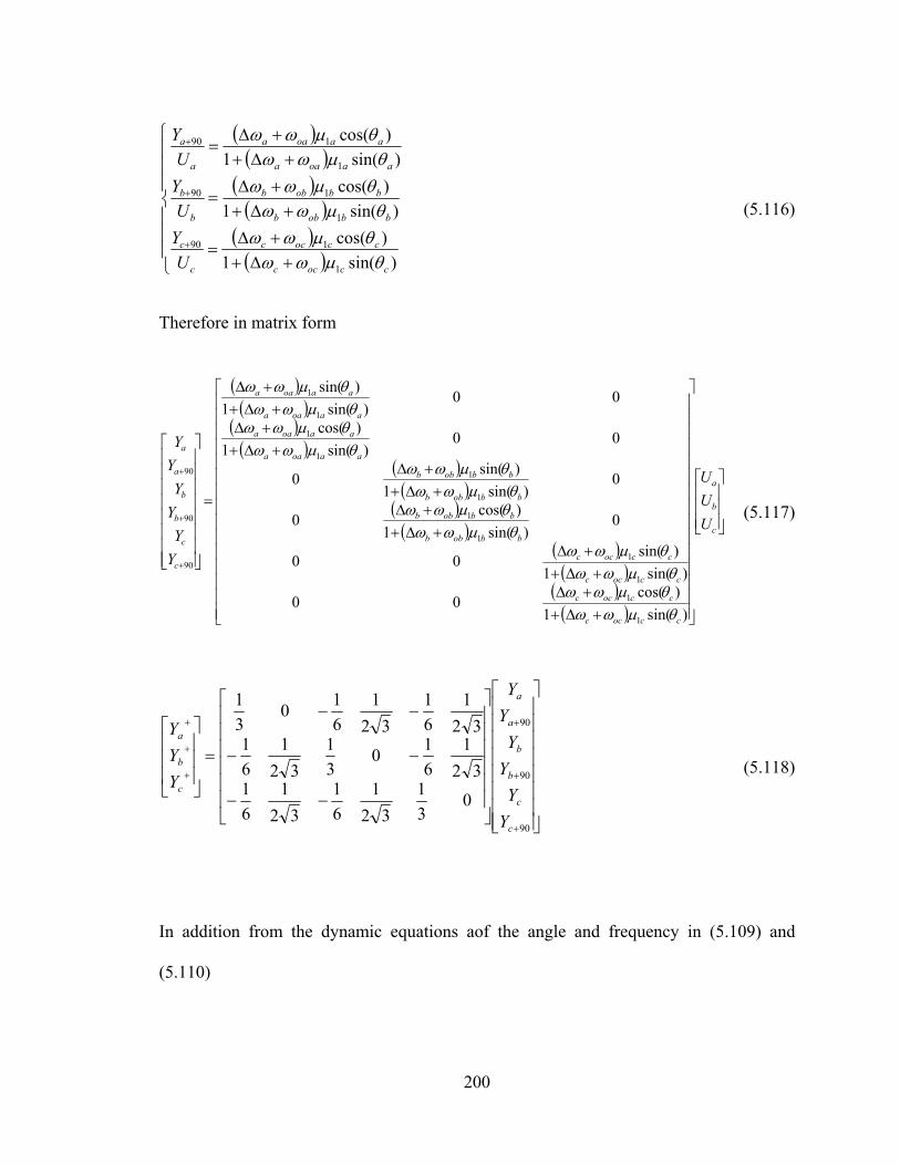
200
)sin(1
)cos(
)sin(1
)cos(
)sin(1
)cos(
1
190
1
190
1
190
ccocc
ccocc
c
c
bbobb
bbobb
b
b
aaoaa
aaoaa
a
a
U
Y
U
Y
U
Y
(5.116)
Therefore in matrix form
c
b
a
ccocc
ccocc
ccocc
ccocc
bbobb
bbobb
bbobb
bbobb
aaoaa
aaoaa
aaoaa
aaoaa
c
c
b
b
a
a
U
U
U
Y
Y
Y
Y
Y
Y
)sin(1
)cos(00
)sin(1
)sin(00
0)sin(1
)cos(0
0)sin(1
)sin(0
00)sin(1
)cos(
00)sin(1
)sin(
1
1
1
1
1
1
1
1
1
1
1
1
90
90
90
(5.117)
90
90
90
03
1
32
1
6
1
32
1
6
132
1
6
10
3
1
32
1
6
132
1
6
1
32
1
6
10
3
1
c
c
b
b
a
a
c
b
a
Y
Y
Y
Y
Y
Y
Y
Y
Y
(5.118)
In addition from the dynamic equations aof the angle and frequency in (5.109) and
(5.110)

201
)cos(
)cos(
)cos(
)cos(
)cos(
)cos(
)cos(00
)cos(00
0)cos(0
0)cos(0
00)cos(
00)cos(
2
3
2
3
2
3
2
3
2
3
2
3
cycc
c
cycc
cocc
bybb
a
bybb
bobb
ayaa
a
ayaa
aoaa
c
b
a
cc
c
cc
c
bb
b
bb
b
aa
a
aa
a
c
c
b
b
a
a
YA
YA
YA
YA
YA
YA
Y
Y
Y
A
A
A
A
A
A
p
(5.119)
If we consider
c
b
a
c
c
b
b
a
a
U
U
U
a
a
a
a
a
a
Y
Y
Y
Y
Y
Y
6
5
4
3
2
1
90
90
90
00
00
00
00
00
00
(5.120)
)cos(
)cos(
)cos(
)cos(
)cos(
)cos(
00
00
00
00
00
00
2
3
2
3
2
3
6
5
4
3
2
1
cycc
c
cycc
cocc
bybb
a
bybb
bobb
ayaa
a
ayaa
aoaa
c
b
a
c
c
b
b
a
a
YA
YA
YA
YA
YA
YA
Y
Y
Y
c
c
c
c
c
c
p
(5.121)

202
Substitude (5.118) and (5.120) into (5.121), the transfer function of the angle and
frequency dynamic equations, from the output to input of the total EPLL for the three
phase system is
)cos(
)cos(
)cos(
)cos(
)cos(
)cos(
ac3
1ac
32
1+ac
6
1ac
32
1+ac
6
1
ac3
1ac
32
1+ac
6
1ac
32
1+ac
6
1
ac32
1+ac
6
1ac
3
1ac
32
1+ac
6
1
ac32
1+ac
6
1ac
3
1ac
32
1+ac
6
132
1
6
1
32
1
6
1
3
132
1
6
1
32
1
6
1
3
1
2
3
2
3
2
3
5646362616
5545352515
6454342414
6353332313
6252423212
6151413111
cycc
c
cycc
cocc
bybb
a
bybb
bobb
ayaa
a
ayaa
aoaa
c
b
a
c
c
b
b
a
a
YA
YA
YA
YA
YA
YA
U
U
U
acacacacac
acacacacac
p
(5.122)
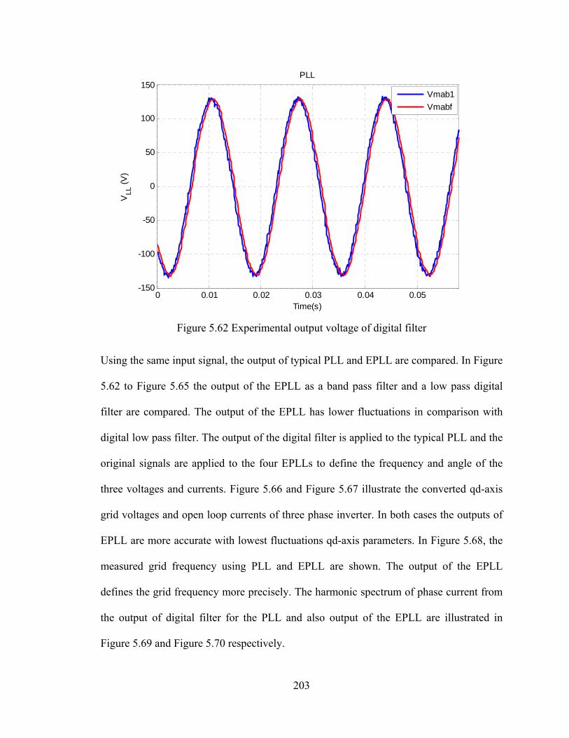
203
0 0.01 0.02 0.03 0.04 0.05-150
-100
-50
0
50
100
150
Time(s)
VLL
(V
)
PLL
Vmab1
Vmabf
Figure 5.62 Experimental output voltage of digital filter
Using the same input signal, the output of typical PLL and EPLL are compared. In Figure
5.62 to Figure 5.65 the output of the EPLL as a band pass filter and a low pass digital
filter are compared. The output of the EPLL has lower fluctuations in comparison with
digital low pass filter. The output of the digital filter is applied to the typical PLL and the
original signals are applied to the four EPLLs to define the frequency and angle of the
three voltages and currents. Figure 5.66 and Figure 5.67 illustrate the converted qd-axis
grid voltages and open loop currents of three phase inverter. In both cases the outputs of
EPLL are more accurate with lowest fluctuations qd-axis parameters. In Figure 5.68, the
measured grid frequency using PLL and EPLL are shown. The output of the EPLL
defines the grid frequency more precisely. The harmonic spectrum of phase current from
the output of digital filter for the PLL and also output of the EPLL are illustrated in
Figure 5.69 and Figure 5.70 respectively.

204
0 0.01 0.02 0.03 0.04 0.05-150
-100
-50
0
50
100
150
Time(s)
VLL
(V
)
EPLL
Vmab1
Vmabf
Figure 5.63 Experimental output voltage of EPLL
0 0.01 0.02 0.03 0.04 0.05-1.5
-1
-0.5
0
0.5
1
1.5
Time(s)
Is1
(A)
PLL
Is1a
Is1af
Figure 5.64 Experimental output current of digital filter

205
0 0.01 0.02 0.03 0.04 0.05-1.5
-1
-0.5
0
0.5
1
1.5
Time(s)
Is1
(A)
EPLL
Is1a
Is1af
Figure 5.65 Experimental output current of EPLL
0 0.01 0.02 0.03 0.04 0.0572
74
76
78
Time(s)
Vm
q (V
)
PLL
EPLL
0 0.01 0.02 0.03 0.04 0.05-4
-2
0
2
4
Time(s)
Vm
d (V
)
PLL
EPLL
Figure 5.66 Experimental qd-axis voltage output of PLL and EPLL
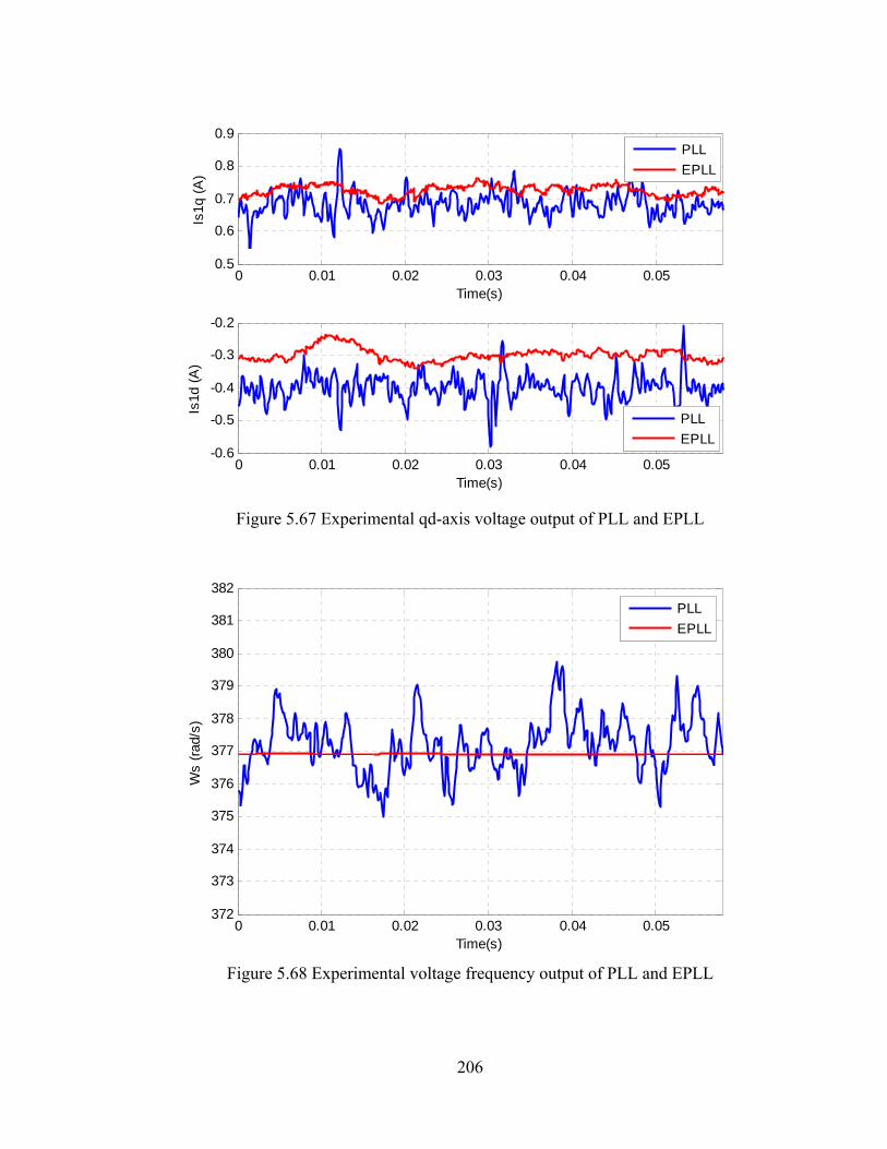
206
0 0.01 0.02 0.03 0.04 0.050.5
0.6
0.7
0.8
0.9
Time(s)
Is1q
(A
)
PLL
EPLL
0 0.01 0.02 0.03 0.04 0.05-0.6
-0.5
-0.4
-0.3
-0.2
Time(s)
Is1d
(A
)
PLL
EPLL
Figure 5.67 Experimental qd-axis voltage output of PLL and EPLL
0 0.01 0.02 0.03 0.04 0.05372
373
374
375
376
377
378
379
380
381
382
Time(s)
Ws
(rad
/s)
PLL
EPLL
Figure 5.68 Experimental voltage frequency output of PLL and EPLL

207
Figure 5.69 Harmonic spectrum of phase current of the digital filter for PLL, fundamental
frequency is 20 times reduced scale.
Figure 5.70 Harmonic spectrum of output phase current of EPLL, fundamental frequency is 20 times reduced scale.

208
Figure 5.71 Hardware experimental setup
Figure 5.72 Relay driver PCB board

209
5.9 Connection of the PV, Battery and Three Phase Inverter
Most part of the experimental setup is shown in Figure 5.71. The configuration is
like Figure 3.1 with three different converters, LC filter and local loads. An automatic
relay connects the system to the main grid. As shown in Figure 5.72, an interface circuit
is designed to close the relay from DSP in a specific programmed moment. Before
connection of the system to the main grid, the synchronization process is investigated. As
shown in Figure 5.73, the channel one of the oscilloscope shows the reference line to line
grid voltage and the channel three presents the output voltage of the inverter after the LC
filter at the point of common coupling (PCC). The reference of the qd-axis of inverter is
changed from 0.85pu to 1 pu. The objective is to verify to different responses, at first the
speed response of the voltage controller for tracking the reference, secondly the operation
of the EPLL in tacking the angle and frequency of the main grid voltage. As shown in the
zoomed graph, the inverter voltage tracks the references in less than one cycle and due to
the precise operation of the EPLL, it matches the grid voltage and is ready to be
connected. The system under local load is operated autonomously. The system dynamic
behavior is investigated in different situations from autonomous operation to grid
connected mode operation. At three different instants, the operation condition is changed.
As shown in Figure 5.74 and Figure 5.75 at the system is working in autonomous mode
before 0.1s. The Figure 5.74 shows the output active and reactive power of the inverter.
In this mode, the just the inverter is feeding the local load and the power of the grid is
zero in Figure 5.75. From 0.1s to 0.22s is the synchronization process and the system is

210
Figure 5.73 Experimental closed loop inverter voltage and current controller response
0 0.05 0.1 0.15 0.2 0.25 0.3 0.35 0.4 0.450
50
100
150
Ps1
(W)
0 0.05 0.1 0.15 0.2 0.25 0.3 0.35 0.4 0.45-40
-20
0
20
Qs1
(Var
)
time(s)
(1) (2) (3) (4)
(1) (2) (3) (4)
Figure 5.74 Experimental active and reactive power of the inverter in both autonomous and grid connected modes.

211
connected to the main grid. Still the active and reactive powers of the grid are almost
zero. Due to the change of the voltage exactly synchronized to the grid with zero d-axis
voltage in Figure 5.77 there is a slight change in the output reactive power of the inverter.
At the instant of the 0.22s the droop controller is transferring the maximum power of the
PV source to the local load and the main grid which is 50W. To transfer the maximum
power of the PV and also to operate in unity power factor and keep the output reactive
power of the inverter zero the voltage angle and frequency from the active power droop
control and the voltage magnitude from the reactive power droop control are varied.
Therefore there is slight change in the power of the voltage dependent local load in
Figure 5.76. The excessive power of the inverter flows into the main grid in Figure 5.75.
In addition at 0.33s the irradiation level of the sun is changed and maximum power of the
PV source also varies to 100W. The reactive power is kept constant. Due to almost
constant load, the active power flows into the grid is increase corresponding to the PV
source output.
The output current of the inverter are tracking the references in Figure 5.78. The line to
line voltage and phase current of the inverter are shown in Figure 5.79. In the moment of
the change of PV irradiation level and its maximum power, change of the output current
is obvious. Moreover the change of the output power causes a slight fluctuation in the
DC-link voltage. The controller part of the bidirectional converter returns the DC link
voltage to its reference (100V) very fast in Figure 5.80.
To show the charging mode of the battery in autonomous mode, the AC load is
reduced suddenly at 2s. As it is shown in Figure 5.81 since the irradiation level of the sun
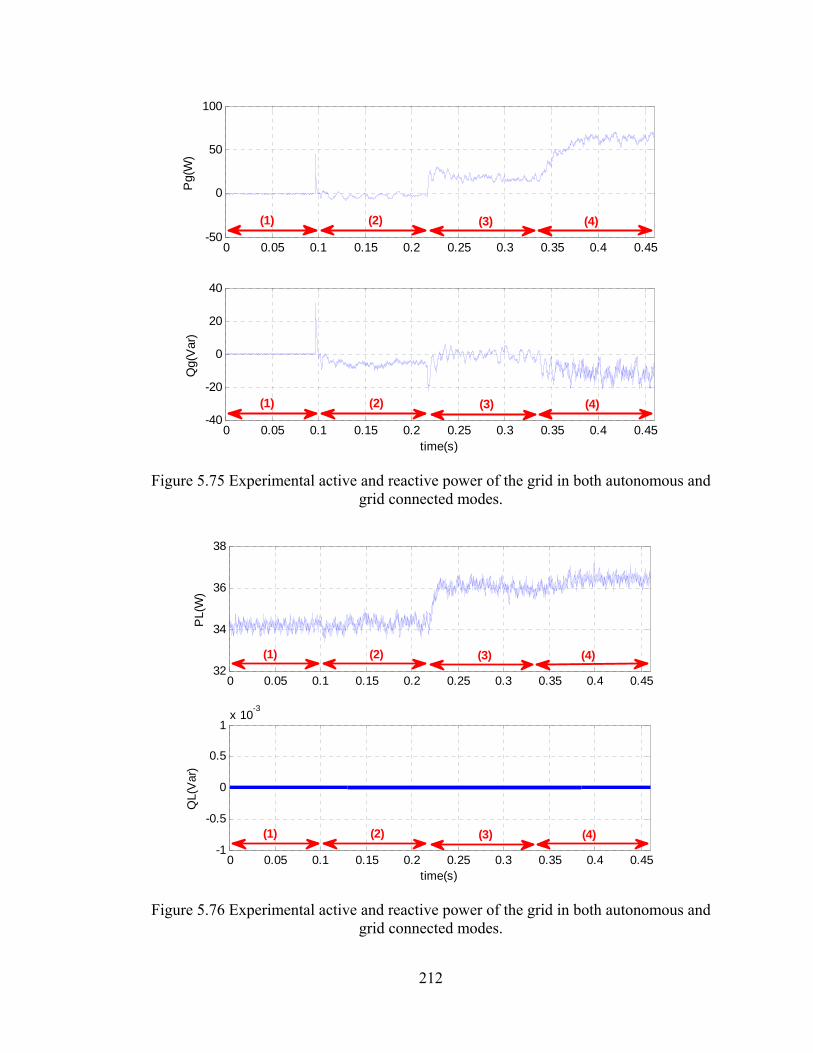
212
0 0.05 0.1 0.15 0.2 0.25 0.3 0.35 0.4 0.45-50
0
50
100
Pg(
W)
0 0.05 0.1 0.15 0.2 0.25 0.3 0.35 0.4 0.45-40
-20
0
20
40
Qg(
Var
)
time(s)
(1) (2) (3) (4)
(1) (2) (3) (4)
Figure 5.75 Experimental active and reactive power of the grid in both autonomous and grid connected modes.
0 0.05 0.1 0.15 0.2 0.25 0.3 0.35 0.4 0.4532
34
36
38
PL(
W)
0 0.05 0.1 0.15 0.2 0.25 0.3 0.35 0.4 0.45-1
-0.5
0
0.5
1x 10
-3
QL(
Var
)
time(s)
(1) (2) (3) (4)
(1) (2) (3) (4)
Figure 5.76 Experimental active and reactive power of the grid in both autonomous and grid connected modes.
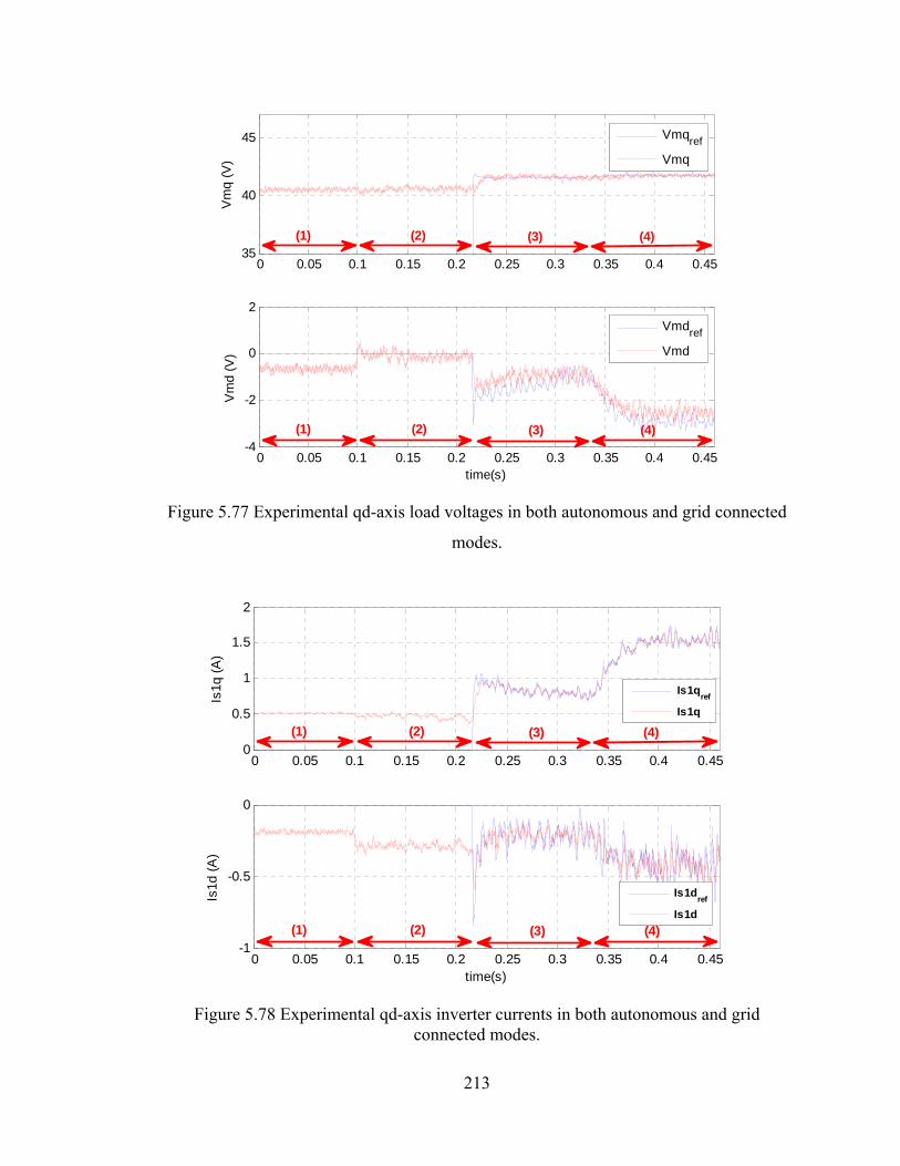
213
0 0.05 0.1 0.15 0.2 0.25 0.3 0.35 0.4 0.4535
40
45
Vm
q (V
)
Vmqref
Vmq
0 0.05 0.1 0.15 0.2 0.25 0.3 0.35 0.4 0.45-4
-2
0
2
Vm
d (V
)
time(s)
Vmdref
Vmd
(1) (2) (3) (4)
(1) (2) (3) (4)
Figure 5.77 Experimental qd-axis load voltages in both autonomous and grid connected
modes.
0 0.05 0.1 0.15 0.2 0.25 0.3 0.35 0.4 0.450
0.5
1
1.5
2
Is1q
(A
)
Is1qref
Is1q
0 0.05 0.1 0.15 0.2 0.25 0.3 0.35 0.4 0.45-1
-0.5
0
Is1d
(A
)
time(s)
Is1dref
Is1d
(1) (2) (3) (4)
(1) (2) (3) (4)
Figure 5.78 Experimental qd-axis inverter currents in both autonomous and grid connected modes.

214
Figure 5.79 Experimental voltage and current of the inverter with changing of the PV
source in grid connected mode, Ch1: Vmab, Ch3:Is1a
Figure 5.80 Experimental DC-link voltage after connection to the grid and change of reference power
215
is constant, the PV output voltage and current remain the same. Figure 5.82 illustrates the
DC-link voltage and the output current of the battery. When the load is reduced in the
constant PV source output, to fulfill the power balance, the excessive current flows into
the battery therefore, the mode of the battery in the bidirectional DC-DC converter
changes from discharging to charging mode. In addition, the battery converter controller
keeps the DC-link voltage constant.
5.10 Conclusions
In this chapter the experimental setups are designed and tested to verify the proposed
system structure and controller design. Due to the complexity of the system, the whole
system is separated into different sections. The design process for each section is
explained in detail and tested autonomously. Then the combined system results are
analyzed. In the first section a 3kW, 50kHz boost converter is designed. Based on the
designed parameters, the appropriate equipment pieces are chosen from the market. The
high frequency inductor is designed and built using ferrite core and Litz wire to reduce
the eddy current effect in high frequencies. The power circuit of the boost converter is
designed in PCB and has been built and soldered. The open loop test in different duty
ratios is applied and sampled with a duty ratio of 0.6 and 68 V as input voltage is shown.
The output voltage after capacitor filter is DC with the lowest fluctuation and the
expected voltage magnitude
The closed loop control of the PV source using a DC/DC boost converter is
applied. A programmable DC source power supply with nonlinear characteristics is
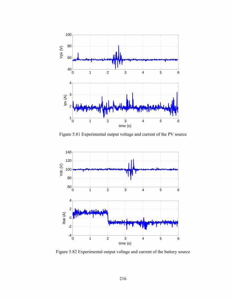
216
0 1 2 3 4 5 640
60
80
100
Vpv
(V
)
0 1 2 3 4 5 61
2
3
4
Ipv
(A)
time (s)
Figure 5.81 Experimental output voltage and current of the PV source
0 1 2 3 4 5 660
80
100
120
140
Vdc
(V
)
0 1 2 3 4 5 6-4
-2
0
2
4
Ibat
(A
)
time (s)
Figure 5.82 Experimental output voltage and current of the battery source

217
connected to an autonomous resistive load though the boost converter. The driver circuit,
DC voltage sensor and DC current sensor boards are designed. The observation and
perturbation method is used to get maximum possible power from the source. For the
control part, the ezDSPF28335 is used and the entire program is written using C language
inside the DSP. Two closed loop tests are applied to show the dynamic and steady state
behavior of the system. The results show that the control algorithm can find the
maximum power point in a few seconds which seems to be a satisfactory response for a
PV source which usually doesn’t change very fast.
In the next step, the three phase inverter and its interface isolator board is
designed. Three phase sinusoidal pulse with modulation (SPWM) signals are produced
inside the DSPF28335. The zero sequence is added to the typical SPWM signals. A look
up table for sinusoidal waveform with 512 samples is used to be compared with an
isosceles triangle carrier waveform of 5KHz. The continuous switching signals and
output inverter voltage under a fixed 60Hz modulation index is produced even with a
modulation index bigger than unity. An interface circuit is designed to connect the DSP
to the three phase inverter module and gate drivers. The output open loop results under
the resistive and under RL load with the 200V input DC link voltage are presented. The
output voltage and current waveforms prove the performance of the written programs in
the DSP for added zero sequence SPWM three phase inverter to increase the linear
modulation region.
The phase lock loop (PLL) software for a three phase system is programmed DSP.
After tuning the voltage sensor, the PLL program is tested experimentally using the
operation of a three phase inverter based on the measured frequency and phase angle of

218
the grid voltage. The results show that the output voltage of the inverter follows the
frequency and angle of the grid precisely.
For synchronization process, the effects of dead time and filter delay are
considered. After the synchronization process the inverter with constant input DC source
is connected to the grid. Using the measured signals, a closed loop PI controller is
designed inside DSP to control reference active and reactive power and also current
references.
At higher voltages, the current has a fifth harmonic causing disturbance in the
power. The harmonic spectrum of the inverter output voltage and currents are shown.
Attenuation of the harmonic voltage was attempted with synchronous PWM modulation.
The switching frequency is chosen to be an integer multiple of 3fs, where fs is the grid
frequency. The experimental results show how the actual powers are tracking the
references after successful synchronization and connection of the DG unit to the main
grid.
Along with the PLL, the enhanced phase lock loop (EPLL) also is designed and
the experimental results of both systems are compared. EPLL is used to define the
reference frequency and angle of the load voltage. It also operates as a band pass filter for
the other parameters like the inverter and grid currents. The outputs of EPLL have lower
noise and therefore EPLL tracks the magnitudes, angles and frequencies of the actual
input signals more precisely.
219
CHAPTER 6
6.DYNAMIC OPERATION AND CONTROL OF GRID
COONECTED INTERIOR PERMANENT MAGNET WIND
TURBINE GENERATOR
6.1 Introduction
Recently, the development amount of the renewable energies such as photo
voltaic (PV), geothermal, and wind energy has been increased significantly. Remarkable
developments have been made with wind turbines during the last decade as a pollution
free and renewable source to supplement other electricity generations.
Most of the wind turbines are variable speed to get more power from the same
wind regime in comparison with fixed speed wind turbines. They also mostly use either
doubly fed induction generator or synchronous generator.
Permanent magnet (PM) machines are one of the most popular kinds of
synchronous machines in wind turbine applications because without the need for
excitation, they offer several interesting features including maintenance-free operation,
high efficiency and reliability, high power factor, and low inertia [119]. Permanent
magnet synchronous machines with approximately sinusoidal back electromotive force
can be broadly categorized into two types; 1) interior (or buried) permanent magnet
machines (IPM) and 2) surface-mounted permanent magnet machines (SPM).
In the interior permanent magnet structure, the equivalent air gap is not uniform
and it makes the saliency effect obvious. The quadrature-axis synchronous inductance of

220
IPM is usually larger than its direct-axis inductance [120], i.e., sdsq LL , which
significantly changes the torque production mechanism. Therefore, both magnetic and
reluctance torque can be produced by the IPM machine [121]. In the second category, the
magnets are mounted on the surface of the rotor. Because the magnets have high
reluctance, the SPM machine can be considered to have a large and uniform effective air
gap. This property makes the saliency effect negligible. Thus the quadrature-axis
synchronous inductance of the SPM machine is equal to its direct-axis inductance, i.e.,
sdsq LL [122]. As a result, only magnet torque can be produced by the SPM machine,
which arises from the interaction of the magnet flux and the quadrature-axis current
component of stator currents ( sqI ). Compared to the SPM machine, the IPM machine has
a mechanically robust and solid structure since the magnets are physically contained and
protected. It also contains both reluctance and magnetic torque which causes higher
efficiency and operation in a wider speed range.
In this chapter the dynamic model of interior permanent magnet machine as a
wind turbine generator is studied. An AC-DC-AC converter connects the wind turbine to
the main grid [123]. Control parts are designed to get maximum power from the wind,
keep DC link voltage constant, and guarantee unity power factor operation. Loss
minimization of the generator is also included. The proportional-integral (PI) controllers
are used for the voltage, speed and inner current control loops. The system is simulated in
MATLAB/Simulink software and the results presented including the most important state
variables and parameters.
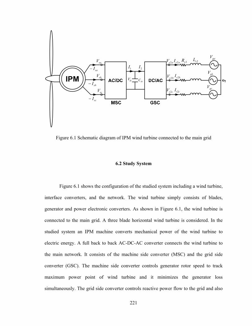
221
2sR 2sLasI 2
bsI 2
csI 2
dcVdcC
asV 2
bsV 2
csV 2
saV
sbV
scV
1I 2IsaI
sbI
scI
gaV
gbV
gcV
Figure 6.1 Schematic diagram of IPM wind turbine connected to the main grid
6.2 Study System
Figure 6.1 shows the configuration of the studied system including a wind turbine,
interface converters, and the network. The wind turbine simply consists of blades,
generator and power electronic converters. As shown in Figure 6.1, the wind turbine is
connected to the main grid. A three blade horizontal wind turbine is considered. In the
studied system an IPM machine converts mechanical power of the wind turbine to
electric energy. A full back to back AC-DC-AC converter connects the wind turbine to
the main network. It consists of the machine side converter (MSC) and the grid side
converter (GSC). The machine side converter controls generator rotor speed to track
maximum power point of wind turbine and it minimizes the generator loss
simultaneously. The grid side converter controls reactive power flow to the grid and also

222
it keeps DC link voltage at a constant value. A voltage source is considered as the main
grid which is connected to the converters though a transmission line. The resistance of
the line also includes the converter switching loss.
6.3 Wind Turbine Model
The power and torque extracted from the wind using wind turbine can be
calculated as follows [121]
3),(2
1wpT VCAP
(6.1)
3),(2
1wp
TT VCAT
(6.2)
w
T
V
R
(6.3)
)17.0(2 )6.5022.0(5.0 eCp (6.4)
where p is the air density, )( 2RA is area swept by the rotor, pC is the power
coefficient, wV is the wind speed, is tip speed ratio, is rotor blade pitch angle, R is
the turbine rotor radius and T is angular speed of the turbine shaft. Table 6.1 shows
parameters of wind turbine.

223
Table 6.1 Wind turbine parameters
1.225 Kg/m3 0 deg
R 5.5 m gearn 6
ratedwV 10 m/s ratedTP 24kW
At a particular wind velocity, the amount of power generated by the turbine
depends upon the speed of the turbine, turbine parameters, and the air density. The air
density is usually assumed to be constant. Turbine parameters are determined by its
design and are constant; so for a fixed blade pitch angle, the output power of the turbine
is mainly dependent on the turbine speed. In Figure 6.2 power coefficient versus tip speed
ratio of the wind turbine at zero pitch angle is illustrated. To get maximum power in a
constant pitch angle, we should choose maximum power coefficient ( 418.0max pC at
0 ) which corresponds to 48.11 .
Figure 6.3 shows the nonlinear power–speed characteristics of the turbine. The
characteristic shifts as the wind speed ( wV ) varies. Each power–speed curve is
characterized by a unique turbine speed ( rMPP ) corresponding to the maximum power
point (MPP) for that wind speed. In addition, for a given wind speed, the maximum
power can be extracted if the turbine is rotated at rMPP . Mechanical model of the turbine
is as follows:
etr TTsp
J )2
( (6.5)

224
where p , J and r are the number of poles, inertia and electrical angular rotor velocity
of generator respectively. tT and eT are wind turbine torque and generator
electromechanical torque.
6.3.1 Defining MPP in Wind Turbine
To define maximum power point extracted from each wind speed [124]
0),(
2
1 3 T
pw
T
T
d
d
d
dCVA
d
dP
(6.6)
where Tgearr n and wT V
R
d
d
, threfore
0)6.5022.0(17.01 2 (6.7)
Thus in maximum power point
6.5022.017.0
1 2 MPP (6.8)
)17.0(2 )6.5022.0(5.0 MPPeC MPPpMPP
(6.9)
R
V
nwMPP
gear
rMPPTMPP
(6.10)
3_2
31 optroptTMPPoptTMMP kkP
(6.11)
where
225
31 )/(
2
1MPPpMPPopt RCAk
(6.12)
3
22
gear
optopt
n
kk
(6.13)
22 rMMPopt
rMPP
TMMPTMMP k
PT
(6.14)
Therefore in any wind speed and pitch angle we will define the optimum rotor speed of
the generator as reference value for speed control part
R
Vn wMPP
gearrMMP
(6.15)
As shown in Figure 6.2 and Figure 6.3, at each pitch angle and wind speed we can
define power coefficient, tip speed ratio and generator speed with which we can extract
maximum power from the wind.
6.3.2 Pitch Angle Effect
Using (6.4), we can show the effect of pitch angle on power coefficient of wind
turbine. Based on (6.1) and (6.4) in a special wind speed and input power
35.0 w
Tp
VA
PC
(6.16)
Moreover, if yxex )(yWx and W is the Lambert function.

226
5 10 15 20 25 300
0.05
0.1
0.15
0.2
0.25
0.3
0.35
0.4
0.45
TSR
Cp
Beta=0 (deg)
Figure 6.2 Power coefficient versus tip speed ratio at zero pitch angle
0 500 1000 1500 2000 2500 3000 35000
0.5
1
1.5
2
2.5x 10
4
Wrm (RPM)
Pt
(W)
Vw=4(m/s)
Vw=6(m/s)
Vw=8(m/s)Vw=10(m/s)
MPP
Figure 6.3 Power coefficient versus tip speed ratio at zero pitch angle

227
432
1
1
)3
8()
2
3(
!
)()( xxxxx
n
nyW n
n
n
(6.17)
)17.0(2 )6.5022.0(5.0 eCp (6.18)
If pxp CC
)(
12)(5.0 c
px ecC (6.19)
where
17.0
6.5022.0
2
21
c
c
)(2
)(212
21212
5.0)( ccpxccc e
Cceccc (6.20)
)(
221221
5.0ccpx e
CcWccc
(6.21)
2
21)(
221
5.0
c
cceC
cW ccpx
(6.22)
Therefore in any special wind speed and power demand we can define different
combinations of pitch angle and tip speed ratio or pitch angle and wind turbine rotor
speed.
Figure 6.4 and Figure 6.5 show that with increase of pitch angle, maximum power
coefficient reduces which causes a lower output power in a constant wind speed. In
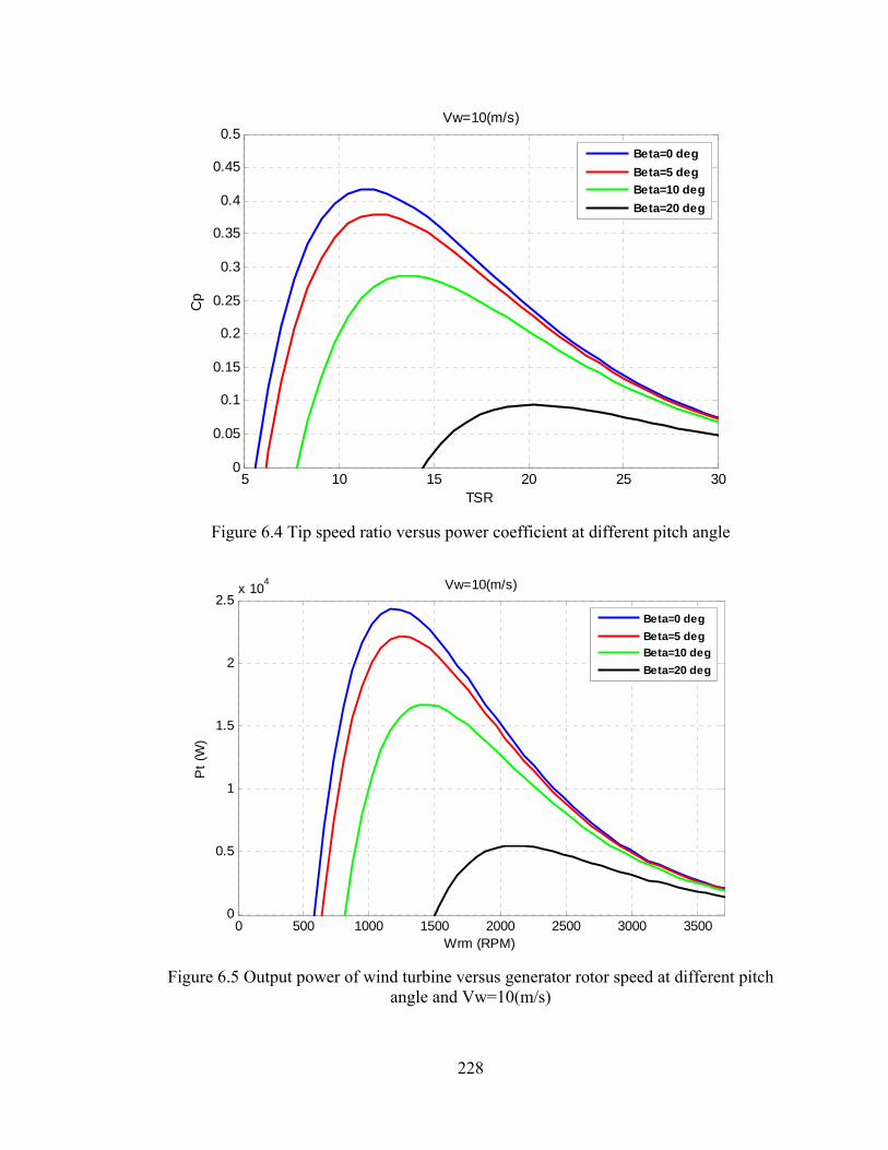
228
5 10 15 20 25 300
0.05
0.1
0.15
0.2
0.25
0.3
0.35
0.4
0.45
0.5
TSR
Cp
Vw=10(m/s)
Beta=0 deg
Beta=5 deg
Beta=10 deg
Beta=20 deg
Figure 6.4 Tip speed ratio versus power coefficient at different pitch angle
0 500 1000 1500 2000 2500 3000 35000
0.5
1
1.5
2
2.5x 10
4
Wrm (RPM)
Pt
(W)
Vw=10(m/s)
Beta=0 deg
Beta=5 deg
Beta=10 deg
Beta=20 deg
Figure 6.5 Output power of wind turbine versus generator rotor speed at different pitch angle and Vw=10(m/s)
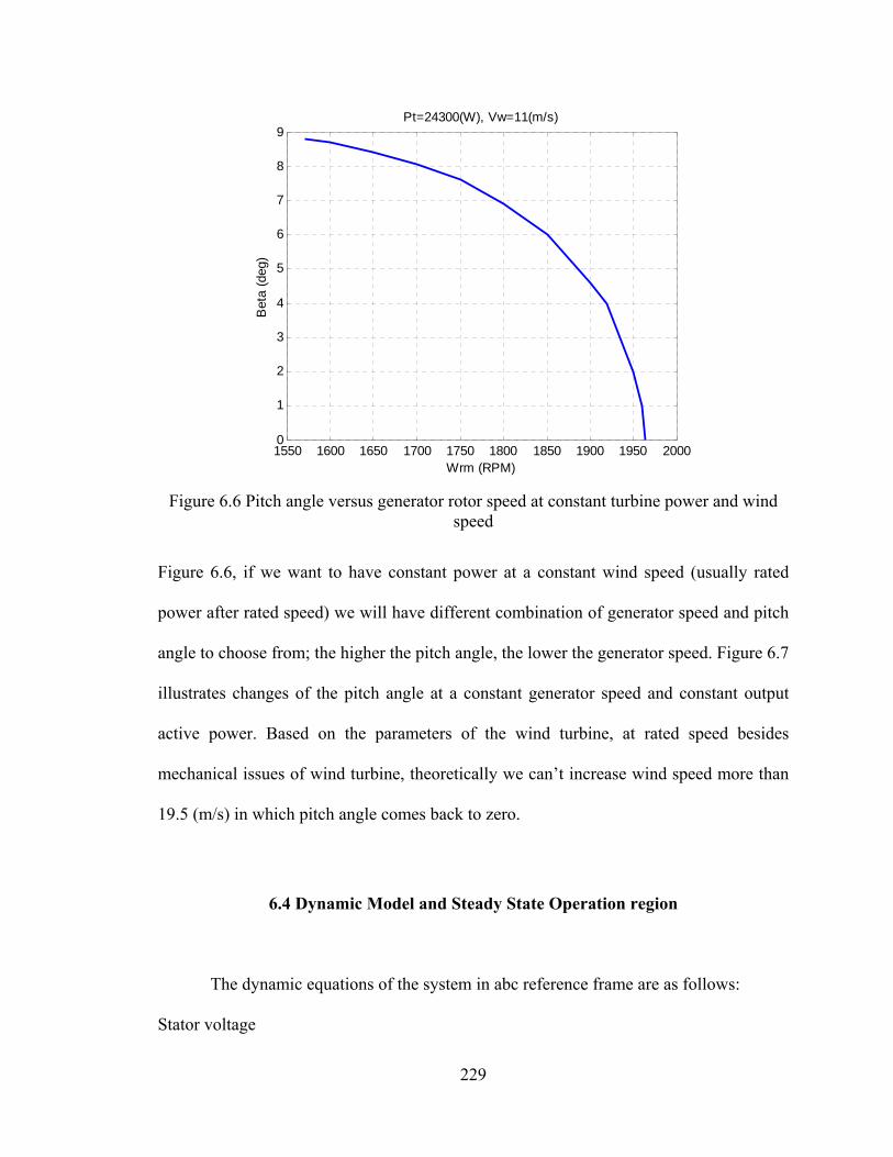
229
1550 1600 1650 1700 1750 1800 1850 1900 1950 20000
1
2
3
4
5
6
7
8
9
Wrm (RPM)
Bet
a (d
eg)
Pt=24300(W), Vw=11(m/s)
Figure 6.6 Pitch angle versus generator rotor speed at constant turbine power and wind speed
Figure 6.6, if we want to have constant power at a constant wind speed (usually rated
power after rated speed) we will have different combination of generator speed and pitch
angle to choose from; the higher the pitch angle, the lower the generator speed. Figure 6.7
illustrates changes of the pitch angle at a constant generator speed and constant output
active power. Based on the parameters of the wind turbine, at rated speed besides
mechanical issues of wind turbine, theoretically we can’t increase wind speed more than
19.5 (m/s) in which pitch angle comes back to zero.
6.4 Dynamic Model and Steady State Operation region
The dynamic equations of the system in abc reference frame are as follows:
Stator voltage

230
10 12 14 16 18 200
1
2
3
4
5
6
7
8
9
Vw (m/s)
Bet
a (d
eg)
Pt=24000 W, Wrm=1200 rpm
Figure 6.7 Wind speed versus pitch angle at the rated output power and rated rotor speed
scscssc
sbsbssb
sasassa
pIRV
pIRV
pIRV
(6.23)
Stator flux
mcscssc
mbsbssb
masassa
IL
IL
IL
(6.24)
Rotor voltage
rcrcrrc
rbrbrrb
rararra
pIRV
pIRV
pIRV
(6.25)

231
Rotor flux
mcrcrrc
mbrbrrb
mararra
IL
IL
IL
(6.26)
Machine side converter equations
nocpdc
nocnsc
nobpdc
nobnsb
noapdc
noansa
VsV
VVV
VsV
VVV
VsV
VVV
)12(2
)12(2
)12(2
1
1
1
(6.27)
cnbnanscsbsano VVVVVVV 3
1
3
1
(6.28)
11
11
11
12
1
12
1
12
1
cpcp
bpbp
apap
Ms
Ms
Ms
(6.29)
Capacitor voltage
)()( 22211121 LccpLbbpLaapsccpsbbpsaapdcdc IsIsIsIsIsIsIIpVC (6.30)
Grid side converter equations

232
222
222
222
)12(2
)12(2
)12(2
nogcLcLLcLcpdc
cs
nogbLbLLbLbpdc
bs
nogaLaLLaLapdc
as
VVpILIRsV
V
VVpILIRsV
V
VVpILIRsV
V
(6.31)
csbsasno VVVV 2222 3
1
(6.32)
22
22
22
12
1
12
1
12
1
cpcp
bpbp
apap
Ms
Ms
Ms
(6.33)
The core loss can be considered as a resistance as follows:
rRcc KR (6.34)
where RcK is a constant coefficient.
If we choose rotor reference frame ( r ), the transformed dynamic equations of
the system to qd-axis reference frame are as follows:
Stator voltages
sqrsdsdssd
sdrsqsqssq
pIRV
pIRV
(6.35)
Rotor voltages
233
rdrdrrd
rqrqrrq
pIRV
pIRV
(6.36)
Stator flux
mrdmdsdsdsd
rqmqsqsqsq
ILIL
ILIL
(6.37)
Rotor flux
msdmdrdrdrd
sqmqrqrqrq
ILIL
ILIL
(6.38)
Torque equation
)(4
3sdsqsqsde II
PT
(6.39)
In permanent magnet machine, the dynamic of the rotor can be neglected since the
permanent magnet is a poor electrical conductor and the eddy currents that flow in the
nonmagnetic materials securing the magnets demagnetization. Therefore
0
0
rd
rq
I
I
(6.40)
mcdsdsdmsdsdsd
cqsqsqsqsqsq
IILIL
IILIL
)(
)(
(6.41)
Substituting (6.41) into (6.35)

234
)()(
)()(
cqsqsqrcdsdsdsdssd
mrcdsdsdrcqsqsqsqssq
IILIIpLIRV
IILIIpLIRV
(6.42)
or
sqsqrsdsdsdssd
mrsdsdrsqsqsqssq
ILIpLIRV
ILIpLIRV
(6.43)
Currents of core loss resistance are
c
sdssd
c
sqr
c
sqsqrsdsdcd
c
sqssq
c
sdr
c
mrsdsdrsqsqcq
R
IRV
RR
ILIII
R
IRV
RR
ILIII
(6.44)
so
sdc
sqsqrsd
sqc
mrsdsdrsq
IR
ILI
IR
ILI
Or
sqsdrc
sqcsqrmsqrsdcsd
sqsdrc
sdsdrcmrcsqcsq
LLR
IRLLIRI
LLR
ILRRIRI
22
22
22
2
(6.45)
Rewriting the torque and voltage equations
sdsqsqsdsqme IILLIP
T )(4
3 (6.46)
sqsqqrsdsddsdssd
sq
sqqmrsdsddrsqsqqsqssq
ILIpLIRV
L
LILIpLIRV
(6.47)
If we use the Thevenin circuit we can also write

235
sqsqrsdsdsdssd
mrsdsdrsqsqsqssq
ILpILIRV
ILpILIRV
(6.48)
where
cs
css RR
RRR
(6.49)
cs
csqsq RR
RVV
(6.50)
cs
csdsd RR
RVV
(6.51)
c
cssqsqq R
RRLL
)(
(6.52)
c
cssdsdd R
RRLL
)(
(6.53)
mqlssq LLL and mdlssd LLL (6.54)
The equivalent circuit of the IPM machine is shown in Figure 6.8. Its Parameters are
presented in Table 6.2
The dynamic equations of the power system and converters are
Machine side converter equations

236
sqsdr IL sdsqr IL sqI sdI
sqV sdV
sqI sdI sR
cRcqI
cdImr
sR
cR
sqL sdL +_+
_
_
+
sqV sdV
sR
sdsddr IL sqsqqr IL sqI sdI sqqL sddL
sR
sq
sqqmr
L
L
Figure 6.8 Equivalent circuits of IPM Machine
Table 6.2 Parameters of the IPM machine and the grid
ratedmV 380 V ratedmI 66.87 A
ratedrm 1200 rpm P (no of poles) 6
sR 0.1764 Ω m 0.246 Wb
sdL 6.24 mH sqL 20.582 mH
dcC 10e-3 F gV 0350 V
2sR 0.01 Ω 2sL 0.4 mH
dcd
sd
dcq
sq
VM
V
VM
V
2
2
1
1
(6.55)
Capacitor equations
)(4
3)(
4
3111121 LddLqqsddsqqdcdc IMIMIMIMIIpVC
(6.56)
Inverter equations
237
gdLqLrLdLLdLdcd
ds
gqLdLrLqLLqLdcq
qs
VILpILIRVM
V
VILpILIRVM
V
2
2
22
22
(6.57)
To define minimum loss operation point
Copper loss equation
22
22 5.1)(2
3sd
c
sqsqrsq
c
mrsdsdrssdsqscopper I
R
ILI
R
ILRIIRP
(6.58)
c
sqmrssqsd
c
sqsdrs
c
sdmsdrs
c
mrssqsqsdsd
c
rssdsqs
copper
R
IRLL
R
IIR
R
ILR
RRILIL
RRIIR
P
3)(33
5.15.1)(5.1
2
2
2
222222
2
222
(6.59)
Core loss equation
22
22 5.1)(2
3
c
sqsqr
c
mrsdsdrccdcqccore R
IL
R
ILRIIRP
(6.60)
c
sdmsdr
c
mrsqsqsdsd
c
rcore R
IL
RILIL
RP
2222222
2
35.15.1 (6.61)
Thus the total loss is
corecopperloss PPP (6.62)
238
c
sqmrssqsd
c
sqsdrs
c
sdmsdrcs
c
mrcssqsqsdsdcs
c
rsdsqs
loss
R
IRLL
R
IIR
R
ILRR
RRRILILRR
RIIR
P
3)(3)(3
)(5.1)(5.1)(5.1
2
2
2
222222
2
222
(6.63)
The output active power of generator
)(2
3sdsdsqsqe IVIVP
(6.64)
sd
c
sqsqrsqsqqrsds
sq
c
mrsdsdr
sq
sqqmrsdsddrsqs
e
IR
ILILIR
IR
IL
L
LILIR
P
2
3
(6.65)
Derivative of output active power versus q-axis stator current
sqsqqrsdsc
sqrsd
c
sqsqrsqqr
sq
sqqmrsdsddrsqssq
c
mrsdsdrs
sq
e
ILIRR
LI
R
ILL
L
LILIRI
R
ILR
I
P
2
3 (6.66)
Derivative of output active power versus d-axis stator current
sqsqqrsdssdc
sqsqrs
sq
sqqmrsdsddrsqs
c
sdrsq
c
mrsdsdrsddr
sd
e
ILIRIR
ILR
L
LILIR
R
LI
R
ILL
I
P
2
3 (6.67)
Derivative of total loss versus q-axis stator current

239
c
mrssqsd
c
sdrssqsqcs
c
rsqs
sq
loss
RRLL
R
IRILRR
RIR
I
P 3)(3)(33 2
2
2
(6.68)
Derivative of total loss versus d-axis stator current
)(3)(3)(33 2
22
2
2
sqsdc
sqrs
c
msdrcssdsdcs
c
rsds
sd
loss LLR
IR
R
LRRILRR
RIR
I
P (6.69)
For minimum loss (optimization) the following determinant should be zero
0
sd
loss
sq
loss
sd
e
sq
e
I
P
I
PI
P
I
P
(6.70)
Moreover due to the use of motor equations, calculated power is negative
therefore
copperT
sdc
sqsqrsqsqqrsds
sqc
mrsdsdr
sq
sqqmrsdsddrsqs
e PP
IR
ILILIR
IR
IL
L
LILIR
P
2
3 (6.71)
Therefore in each wind speed with defining output wind power as follows:
brbT
brTMPPT
PP
PP
(6.72)
And using (6.70) and (6.71) we will have two equations and two variables
( sdsq II , ) which will define the steady state operation region of wind turbine.

240
6.4.1 Steady State Operation under Constant Generator Speed after Nominal
Wind Speed
To keep generator speed or wind turbine speed constant after rated wind speed,
pitch angle should be increased based on Figure 6.7. Figure 6.9 shows after nominal wind
speed (10 (m/s)), with increase of pitch angle, wind turbine rotor speed remains constant
at rated value (1200 rpm). In Figure 6.10, due to constant DC-link voltage, the
modulation index of the converter increases based on the voltage magnitude and it is
always less than unity. In Figure 6.11, magnitudes of qd-axis stator currents are shown.
They are defined in a way that prepare minimum total loss and follow maximum power
point of wind turbine characteristics. Current direction is negative because the motor
equation is used for the generator. Figure 6.12 illustrates output voltage and current
magnitude behavior of the stator. Before rated wind speed, both current and voltage
magnitudes increase then remain constant. Figure 6.13 presents maximum power point
tracking of the wind turbine characteristic and keeping output power constant at rated
value after nominal wind speed using pitch angle control. The small difference between
the input power from wind turbine and the output power of the generator is due to total
loss which is always minimized. In Figure 6.14 efficiency of the generator for total loss
minimization in different wind speeds is shown. With increase of wind speed, efficiency
first decreases and then starts to increase. Total deviation of efficiency is less than 3%
and after nominal wind speed it is fixed at around 95%.
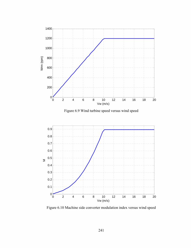
241
0 2 4 6 8 10 12 14 16 18 200
200
400
600
800
1000
1200
1400
Vw (m/s)
Wrm
(rp
m)
Figure 6.9 Wind turbine speed versus wind speed
0 2 4 6 8 10 12 14 16 18 200
0.1
0.2
0.3
0.4
0.5
0.6
0.7
0.8
0.9
Vw (m/s)
M
Figure 6.10 Machine side converter modulation index versus wind speed
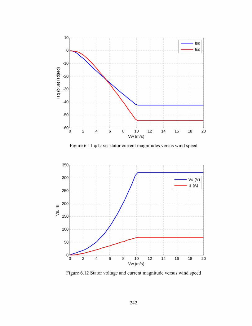
242
0 2 4 6 8 10 12 14 16 18 20-60
-50
-40
-30
-20
-10
0
10
Vw (m/s)
Isq
(blu
e) I
sd(r
ed)
Isq
Isd
Figure 6.11 qd-axis stator current magnitudes versus wind speed
0 2 4 6 8 10 12 14 16 18 200
50
100
150
200
250
300
350
Vw (m/s)
Vs,
Is
Vs (V)
Is (A)
Figure 6.12 Stator voltage and current magnitude versus wind speed

243
0 2 4 6 8 10 12 14 16 18 200
0.2
0.4
0.6
0.8
1
Vw (m/s)
Pge
n (p
u),
Pt
(pu)
Pb=25000
Pgen
Pt
Figure 6.13 Power of wind turbine and output active power of generator versus wind speed
2 4 6 8 10 12 14 16 18 2092.5
93
93.5
94
94.5
95
95.5
96
96.5
Vw (m/s)
Eff
icie
ncy
(Pge
n/P
t)
Figure 6.14 Efficiency versus wind speed
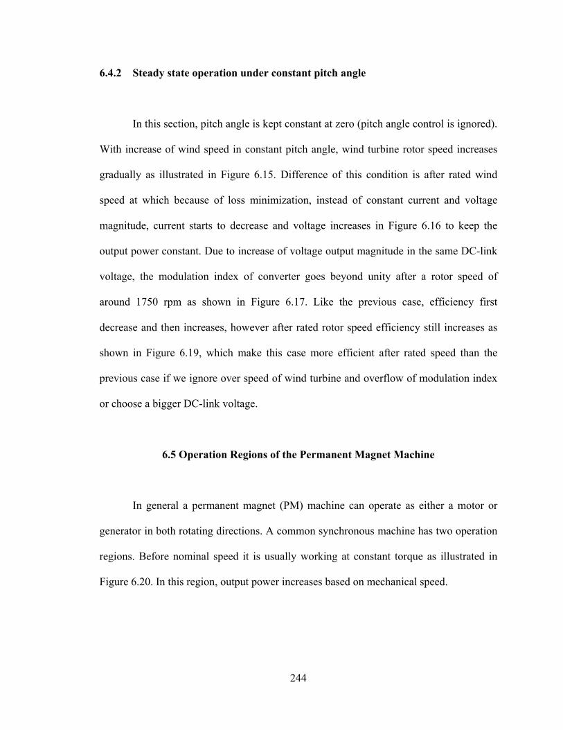
244
6.4.2 Steady state operation under constant pitch angle
In this section, pitch angle is kept constant at zero (pitch angle control is ignored).
With increase of wind speed in constant pitch angle, wind turbine rotor speed increases
gradually as illustrated in Figure 6.15. Difference of this condition is after rated wind
speed at which because of loss minimization, instead of constant current and voltage
magnitude, current starts to decrease and voltage increases in Figure 6.16 to keep the
output power constant. Due to increase of voltage output magnitude in the same DC-link
voltage, the modulation index of converter goes beyond unity after a rotor speed of
around 1750 rpm as shown in Figure 6.17. Like the previous case, efficiency first
decrease and then increases, however after rated rotor speed efficiency still increases as
shown in Figure 6.19, which make this case more efficient after rated speed than the
previous case if we ignore over speed of wind turbine and overflow of modulation index
or choose a bigger DC-link voltage.
6.5 Operation Regions of the Permanent Magnet Machine
In general a permanent magnet (PM) machine can operate as either a motor or
generator in both rotating directions. A common synchronous machine has two operation
regions. Before nominal speed it is usually working at constant torque as illustrated in
Figure 6.20. In this region, output power increases based on mechanical speed.

245
0 2 4 6 8 10 12 14 16 18 200
500
1000
1500
2000
2500
Vw (m/s)
Wrm
(rp
m)
Figure 6.15 Wind turbine speed versus wind speed
0 500 1000 1500 2000 25000
50
100
150
200
250
300
350
400
Wrm (rpm)
Vs,
Is
Vs (V)
Is (A)
Figure 6.16 Stator voltage and current magnitude versus wind speed
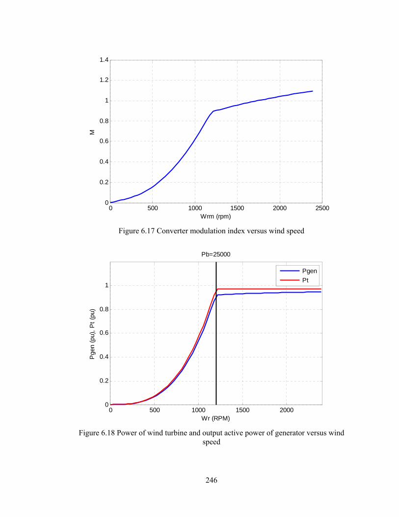
246
0 500 1000 1500 2000 25000
0.2
0.4
0.6
0.8
1
1.2
1.4
Wrm (rpm)
M
Figure 6.17 Converter modulation index versus wind speed
0 500 1000 1500 20000
0.2
0.4
0.6
0.8
1
Wr (RPM)
Pge
n (p
u),
Pt
(pu)
Pb=25000
Pgen
Pt
Figure 6.18 Power of wind turbine and output active power of generator versus wind speed

247
200 400 600 800 1000 1200 1400 1600 1800 2000 2200 240092.5
93
93.5
94
94.5
95
95.5
96
96.5
97
97.5
Wrm (rpm)
Eff
icie
ncy
(Pge
n/P
t)
Figure 6.19 Efficiency versus wind speed
)( pur
Figure 6.20 Power and torque characteristics of PM machine
Once the machine reaches its rated speed, output power remains constant at nominal
value and the torque starts to decrease.
In a permanent magnet synchronous machine, to extend operating speed range,
demagnetizing phase currents are generally applied to weaken the air-gap flux. This is

248
known as flux-weakening control and thus the motor is operated in the flux-weakening
region.
6.5.1 Voltage and Current Constraints of PM Machine
In normal operation, with the speed of the PM motors increasing, the voltage
applied to the motor must increase accordingly in order to counteract the speed-
proportional induced back EMF in the stator windings. When the speed reaches the rated
value, eventually, the voltage applied to the PMSM cannot be further increased to
maintain the current required by torque production. On the other hand, considering the
current capability, the maximum stator current is limited by the current rating of inverter
as well as the thermal rating of stator windings.
Therefore, the maximum output torque and power developed by the PM machine
is ultimately determined by the maximum current and voltage of the machine or the
inverter connected to the machine.
Assume that the voltage applied to the PM machine reaches its limit. The
maximum stator voltage, maxsV , is determined as
max22
ssdsq VVV (6.73)
Hence, at high speeds, the voltage vector should remain on the locus of a circle with
radius maxsV for maximum-power output.
Neglecting the ohmic voltage drop of stator resistance for high-speed operation,
the limit by the maximum stator voltage is expressed in terms of steady-state currents as

249
2
max22 )()( smrsdsdrsqsqr VILIL
(6.74)
It can be seen that the current vector trajectories in the rotor reference frame are
constrained by an ellipse at a specific speed in qd-axis stator current plane. Referring to
the IPM, of which the quadrature-axis stator inductance is larger than the direct-axis
inductance, i.e., Lq>Ld, the minor axis of the ellipse will be in the q-axis current direction.
Figure 6.21 shows the voltage-limited ellipses with respect to different operating
speeds in the flux-weakening region. As illustrated, the voltage constraint determines a
series of nested ellipses, i.e., concentration ellipses, centered at Point A 0,/ sdm L in
the qd-axis stator current plane. As the maximum voltage maxsV is fixed, the ellipse
shrinks inversely with rotor speed r . It should be noted that the shape of the ellipses
depends upon the saliency ratio, which is defined as Lq/Ld. For all nonsaliency PM
machines, e.g., surface-mounted PM motors, the voltage-limited ellipses change to circles
and the corresponding equation is
ssdsq LLL (6.75)
2max
22 )()( smrsdsrsqsr VILIL (6.76)
On the other hand, the current sqI and sdI must satisfy
2
max22
ssdsq III (6.77)
where maxsI is the allowable maximum stator current. This expression represents a
current-limited circle centered at the origin and with the radius of maxsI as shown in
Figure 6.21b.

250
1r
2r
12 rr maxsI
sd
m
L
sqI
sdI
maxsI
sd
m
L
sqI
sdI
1r
2r
s
m
L
12 rr
Figure 6.21 Voltage and current constraints characteristics a) Interior permanent magnet machine b) Surface mounted permanent magnet machine
It should be noticed that this current-limited circle remains constant for any speed
and the instantaneous current sqI and sdI must comply with the maximum current
constraint. In the qd-axis stator current plane, any combination of values of current
component sqI and sdI generates a directed current vector from the origin. To a given
rotor speed, the current vector can reach anywhere inside or on the boundary of the
overlap area between the associated voltage-limited ellipse/circle and the current-limited
circle during steady-state operation but not outside it. The overlap area becomes smaller

251
and smaller and even disappears when the rotor speed keeps increasing, indicating
progressively smaller ranges for the current vector in the flux-weakening region.
6.5.2 Maximum Torque per Ampere (MTPA) Operation (ω≤ωb)
The maximum electromagnetic torque and output power developed by the PM
machine is ultimately dependent on the allowable current rating and the maximum output
voltage.
In a PM machine, which operates at a given speed and torque, optimal efficiency
can be obtained by the application of an optimal voltage that minimizes power losses. At
low speeds, this optimum will coincide with the condition of maximum torque per stator
ampere, assuming the core losses to be negligible. Such operation leads to minimal
copper losses of stator windings and power losses of semiconductor switches in the
power inverter. Furthermore, minimization of the stator current for the given maximum
torque results in a lower current rating of the inverter and thus the coverall cost of the
PMSM drive system is reduced; therefore, in most cases, the MTPA control mode is
preferred for the constant-torque operation of PM machines. As presented previously in
(6.46) the electromagnetic torque consists of
a) Magnet torque, which is proportional to the product of the magnet flux linkage
(i.e., rotor flux in the rotor reference frame) and the quadrature-axis stator current
(i.e., torque producing stator current component).

252
b) Reluctance torque only for PM machines with saliency, which is dependent on the
saliency ratio (d
q
L
L) and the product of the direct-axis the quadrature-axis stator
current components. Hence the electromagnetic torque of PMSM can be
controlled instantaneously through controlling the stator currents in the rotating
reference frame to meet load torque requirements.
If the stator currents are set to their maximum permissible value then, from (6.46), it is
easy to see the maximum torque of SPM motors
maxmax 4
3sme I
PT
(6.78)
where the quadrature-axis current component TsqI max_ equals the maximum current
maxsI while the direct-axis component TsdI max_ is kept zero as
maxmax_
max_ 0
sTsq
Tsd
II
I
(6.79)
As for IPM motors, in contrast, the maximum torque is produced when the stator
current reaches its maximum but both its direct-axis and quadrature-axis component,
TsdI max_ and TsqI max_ respectively, have values in agreement with torque optimization. It
can be calculated as follows:
Torque equation based on stator phase current magnitude and its phase angle
sdsqsqsdsqme IILLIP
T )(4
3 and
sin
cos
sasd
sasq
II
II
(6.80)

253
)sin)(cos)((cos4
3 sasasqsdsame IILLIP
T (6.81)
2sin)(
2
1cos
4
3 2sasdsqsame ILLI
PT
(6.82)
For maximum torque per ampere (MTPA)
02cos)(sin4
3 2 sasdsqsam
e ILLIP
d
dT
(6.83)
0sincos)(sin 222 sasdsqsam ILLI (6.84)
0)()( 22 sdsdsqsqsdsqsdm ILLILLI (6.85)
Relationship between qd-axis stator current in MTPA condition
sdsdsq
msdsq I
LLII
)(2
(6.86)
)(2
)(4 222
sdsq
sqsdsqmm
sd LL
ILLI
)(2
)(4 222
sdsq
sqsdsqmm
sd LL
ILLI
(6.87)
To find the angle of current at MTPA
0sin21)(sinsincos)(sin 22222 sasdsqsamsasdsqsam ILLIILLI(6.88)
0)(sinsin)(2 222 sasdsqsamsasdsq ILLIILL (6.89)

254
0)(sinsin)(2 2 sasdsqmsasdsq ILLILL (6.90)
sasdsq
sasdsqmm
ILL
ILL
)(4
)(8sin
222
(6.91)
sasdsq
sasdsqmm
ILL
ILL
)(4
)(8sin
222
1
(6.92)
and
sin
cos
sasd
sasq
II
II therefore
qd-axis stator current at MTPA ( maxssa II )
)(4
)(8
)(4
)(8sinsin
222222
1max_
sdsq
sasdsqmm
sasdsq
sasdsqmm
saTsd LL
ILL
ILL
ILLII
(6.93)
22max_ sdsaTsq III (6.94)
Another way to calculate qd-axis stator current at MTPA
2222 )(
4
3)(
4
3sdsasdsqsdsdsamsdsqsqsdsqme IIILLII
PIILLI
PT
(6.95)
0)()(
4
3 22
2222
sdsasqsd
sdsa
sdsdsqsd
sdsa
sdm
sd
e IILLII
IILL
II
IP
dI
dT
(6.96)
0)()(2 22 sasqsdsdmsdsqsdsd
e ILLIILLdI
dT (6.97)

255
)(4
)(8
)(4
)(8 222
max__
222
max__sdsq
sasdsqmm
Tsdsqsd
sasqsdmm
Tsd LL
ILLI
LL
ILLI
(6.98)
22max_ sdsaTsq III (6.99)
Base speed of the synchronous machine at MTPA
2max_
2max_
smax
)()( TsqsqTsdsdm
bILIL
V
(6.100)
6.5.3 Maximum Torque per Voltage (MTPV) Operation (Flux Weakening)
(ωb≤ω≤ωc1)
At high speeds (more than nominal speed) in the flux weakening region,
maximum output power is achievable by means of the Maximum Torque per Voltage
(MTPV) control. For a given speed, the maximum torque under both current and voltage
constraints leads to the maximum output power. The current vector trajectory of
maximum torque control in the qd-axis stator current plane is selected as follows:
2222
2222 )()(
sdsqsmaxsa
sqsqsdsdmsmaxsa
IIII
ILILVV
(6.101)
)(
222
22222222422222
22222222222422222
2
sqsd
sasqsasdsqmsqsasdsqsasdm
sdsqsasdmsqmsdsasasqsasd
sqLL
VLVLLLILLIL
LLILLLIVLVL
I
(6.102)

256
)( 22
22222222422222
2
sqsd
sdmsasqsasdsqmsqsasdsqsa
sdLL
LVLVLLLILLII
(6.103)
or from (6.101)
)()( 22222
sdsasqsdsdmsa IILIL
V
(6.104)
02)(2
222222
samsasqsdsdmsqsdsd
VILILLLI
(6.105)
)(
)(
22
22222222
sqsd
samsasqsqsdsdmsdm
sdLL
VILLLLL
I
(6.106)
22sdsasq III (6.107)
6.5.4 Flux Weakening with Stator Current Operation (ω≥ωc1)
Figure 6.22 illustrates three different operation regions of a permanent magnet
machine. In an interior permanent magnet machine if max/ ssdm IL , we can extend the
speed operation region with flux weakening along with current reduction of stator in the
third region. In this condition, the machine is working under nominal voltage ( maxsV ) but
current is decreasing therefore it doesn’t operate under maximum power. The equations
are as follows:

257
b maxsI
sd
m
L
sqI
sdI
max/ ssdm IL
1c
maxsI
sdI
1c
b
sd
m
L
max/ ssdm IL
maxsI
sdI
1
s
m
L
2
31c
b
c)
Figure 6.22 Operation region of PM machine a) Interior permanent magnet machine ( max/ ssdm IL ), b) Interior permanent magnet machine ( max/ ssdm IL ), c) Surface
mounted permanent magnet machine.
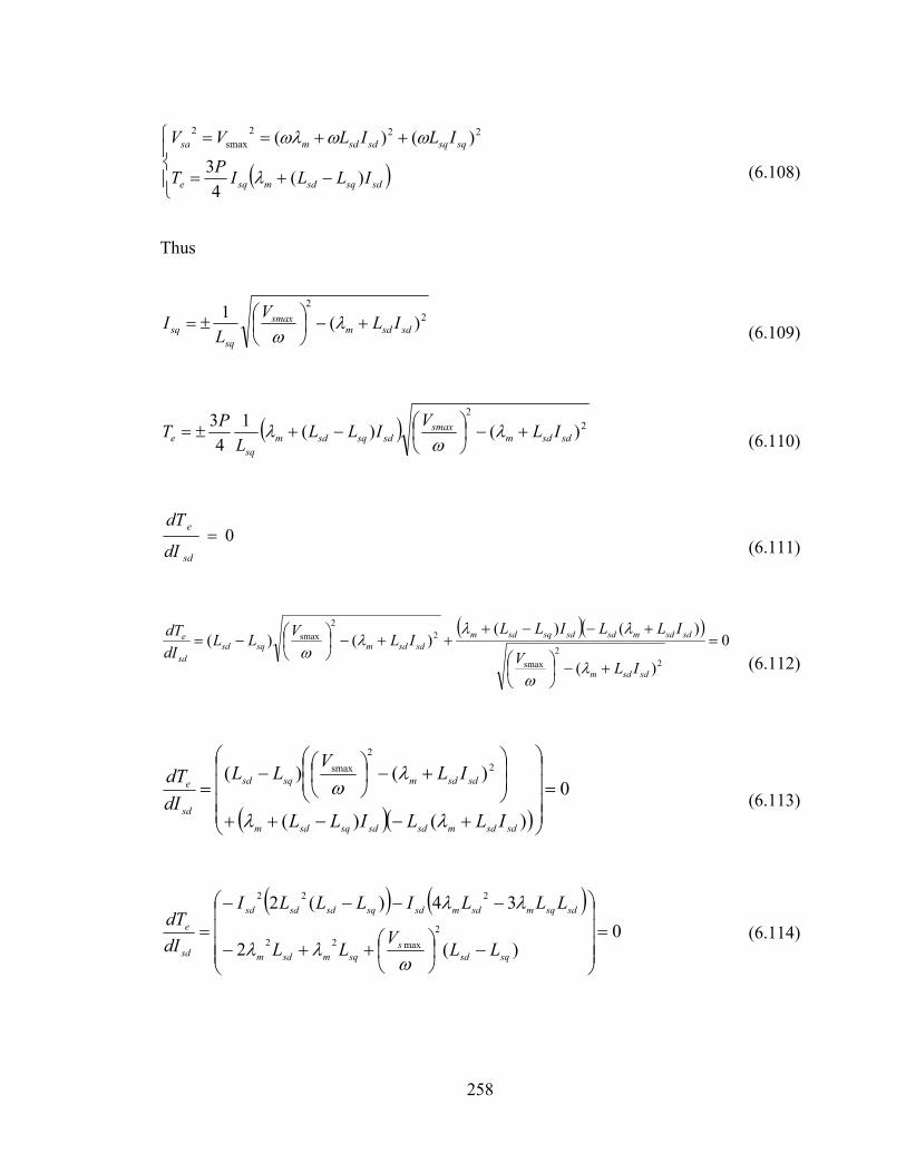
258
sdsqsdmsqe
sqsqsdsdmsa
ILLIP
T
ILILVV
)(4
3
)()( 222smax
2
(6.108)
Thus
22
)(1
sdsdmsmax
sqsq IL
V
LI
(6.109)
22
)()(1
4
3sdsdm
smaxsdsqsdm
sqe IL
VILL
L
PT
(6.110)
0sd
e
dI
dT
(6.111)
0
)(
)()()()(
22
smax
22
smax
sdsdm
sdsdmsdsdsqsdmsdsdmsqsd
sd
e
ILV
ILLILLIL
VLL
dI
dT
(6.112)
0
)()(
)()( 2
2
smax
sdsdmsdsdsqsdm
sdsdmsqsd
sd
e
ILLILL
ILV
LL
dI
dT
(6.113)
0
)(2
34)(22
max22
222
sqsd
ssqmsdm
sdsqmsdmsdsqsdsdsd
sd
e
LLV
LL
LLLILLLI
dI
dT
(6.114)
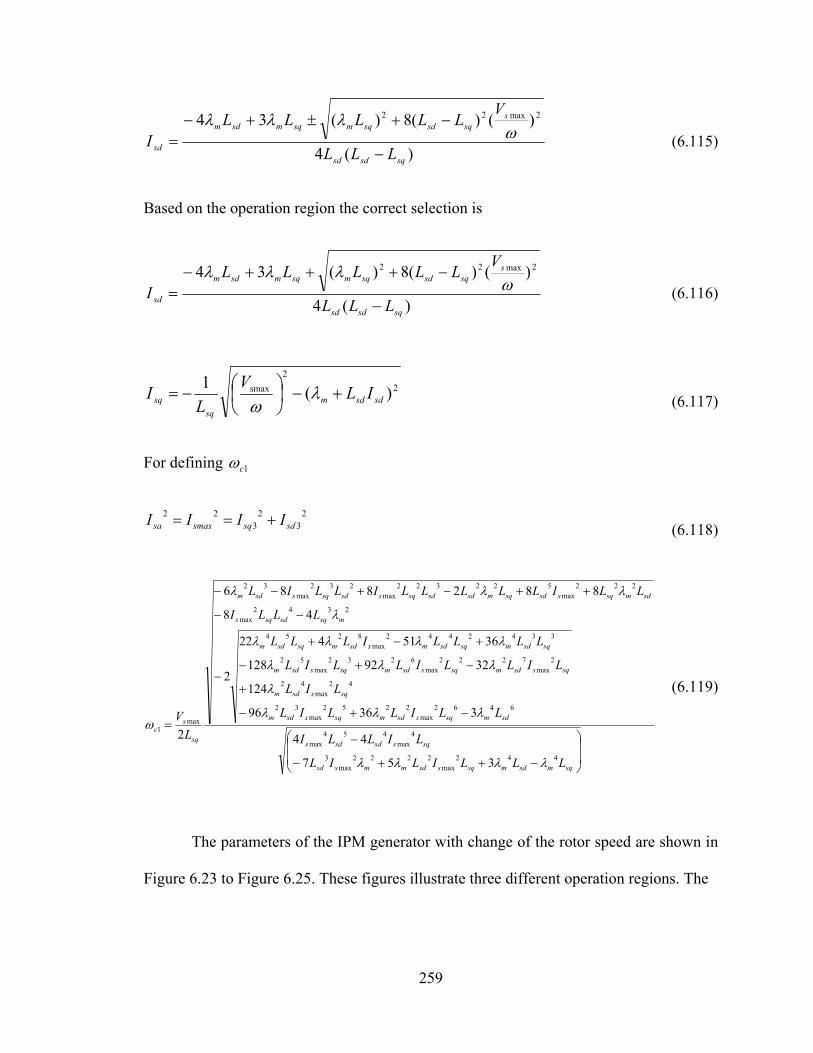
259
)(4
)()(8)(34 2max22
sqsdsd
ssqsdsqmsqmsdm
sd LLL
VLLLLL
I
(6.115)
Based on the operation region the correct selection is
)(4
)()(8)(34 2max22
sqsdsd
ssqsdsqmsqmsdm
sd LLL
VLLLLL
I
(6.116)
2
2
smax )(1
sdsdm
sq
sq ILV
LI
(6.117)
For defining 1c
2
32
322
sdsqsmaxsa IIII (6.118)
sqmsdmsqssdmmssd
sqssdsds
sdmsqssdmsqssdm
sqssdm
sqssdmsqssdmsqssdm
sqsdmsqsdmssdmsqsdm
msqsdsqs
sdmsqssdsqmsdsdsqssdsqssdm
sq
sc
LLLILIL
LILLI
LLILLIL
LIL
LILLILLIL
LLLLILLL
LLLI
LLILLLLLILLIL
L
V
442max
2222max
3
4max
454max
6462max
2252max
32
42max
42
2max
7222max
6232max
52
3342442max
8254
2342max
222max
522322max
232max
32
max1
357
44
33696
124
3292128
3651422
2
48
882886
2
(6.119)
The parameters of the IPM generator with change of the rotor speed are shown in
Figure 6.23 to Figure 6.25. These figures illustrate three different operation regions. The

260
0 1000 2000 3000 4000 5000 6000 7000 8000 9000 10000-60
-40
-20
0
Isqd
(A
)
Isq
Isd
0 1000 2000 3000 4000 5000 6000 7000 8000 9000 1000040
45
50
55
60
Wrm (rpm)
Is (
A)
(3)(2)(1) wb
wc1
Figure 6.23 The qd-axis and magnitude of the IPM stator current
0 1000 2000 3000 4000 5000 6000 7000 8000 9000 10000-200
0
200
400
Vsq
d (V
)
Vsq
Vsd
0 1000 2000 3000 4000 5000 6000 7000 8000 9000 100000
100
200
300
400
Wrm (rpm)
Vs
(V)
(1) (2) (3)wb
wc1
Figure 6.24 The qd-axis and magnitude of the IPM stator voltage

261
0 1000 2000 3000 4000 5000 6000 7000 8000 9000 100000
1
2
3x 10
4
Ps
(W)
0 1000 2000 3000 4000 5000 6000 7000 8000 9000 100000
50
100
150
Wrm (rpm)
Ts
(Nm
)
(1) (2) (3)wb
wc1
Figure 6.25 The output power and torque of the IPM generator
fist region is up to the rated speed. The second region is the flux weakening region 1 and
then the third region is the second flux weakening region.
6.6 Machine Side Converter Controller Design
In connection of the IPM machine to the wind turbine, the base objective is to get
maximum power from the wind. Based on the parameters of wind turbine, we may have
different conditions. First if wind turbine design exactly matches the generator, both
maximum power of the generator and the wind turbine at nominal wind speed are in the
same point as the nominal speed of the generator. Otherwise in other cases, maximum
power happens either before or after nominal speed of generator [119]. Both generator
and wind turbine are assumed to be matched.

262
In interior permanent magnet machine, if we don’t consider the core loss of the
machine, the dynamic equations in rotor reference frame, are as follows:
Stator voltages
21dc
qsdrsqsqssq
VMpIRV
(6.120)
21dc
dsqrsdsdssd
VMpIRV
(6.121)
where sqdV , sqdI and sd are qd-axis voltages, currents and flux linkages of the stator.
1qdM and dcV are qd-axis modulation index of machine side converter and DC link
voltage respectively. sR is the stator resistance.
Rotor voltages
rqrqrrq pIRV (6.122)
rdrdrrd pIRV (6.123)
where rR and rqdI are resistance and qd-axis currents of the rotor.
Stator flux
rqmqsqsqsq ILIL (6.124)
mrdmdsdsdsd ILIL (6.125)
Rotor flux

263
sqmqrqrqrq ILIL (6.126)
msdmdrdrdrd ILIL (6.127)
Torque equation
)(4
3sdsqsqsde II
PT
(6.128)
sqsqsq IL (6.129)
msdsdsd IL (6.130)
mrsdsdrsqsqsqsdc
q ILpILIRV
M 21
(6.131)
sqsqrsdsdsdsdc
d ILpILIRV
M 21
(6.132)
Capacitor equation
21121 )(4
3IIMIMIIpVC sddsqqdcdc
(6.133)
The dynamic equations of the main grid and grid side converter are
dsseqssqssgqdcq ILsILIRVV
M222222
2
2 (6.134)
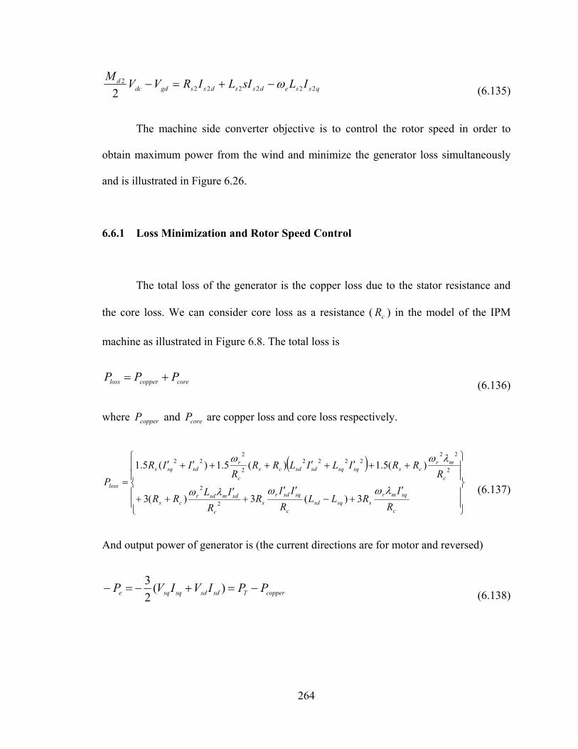
264
qssedssdssgddcd ILsILIRVV
M222222
2
2
(6.135)
The machine side converter objective is to control the rotor speed in order to
obtain maximum power from the wind and minimize the generator loss simultaneously
and is illustrated in Figure 6.26.
6.6.1 Loss Minimization and Rotor Speed Control
The total loss of the generator is the copper loss due to the stator resistance and
the core loss. We can consider core loss as a resistance ( cR ) in the model of the IPM
machine as illustrated in Figure 6.8. The total loss is
corecopperloss PPP (6.136)
where copperP and coreP are copper loss and core loss respectively.
c
sqmrssqsd
c
sqsdrs
c
sdmsdrcs
c
mrcssqsqsdsdcs
c
rsdsqs
loss
R
IRLL
R
IIR
R
ILRR
RRRILILRR
RIIR
P
3)(3)(3
)(5.1)(5.1)(5.1
2
2
2
222222
2
222
(6.137)
And output power of generator is (the current directions are for motor and reversed)
copperTsdsdsqsqe PPIVIVP )(2
3
(6.138)

265
)(sk
wV
r
optr _
eP
lossP
*sqI
*sdI
sqI
sdI
sdr L
qs1
ds1
s
kk qIs
qPs1
1 1qM
1dM
dcV
2
dcV
2
s
kk dIs
dPs1
1
sqrL
mr
Figure 6.26 Machine side converter controller
copperT
sdc
sqsqrsqsqqrsds
sqc
mrsdsdr
sq
sqqmrsdsddrsqs
e PP
IR
ILILIR
IR
IL
L
LILIR
P
2
3(6.139)
where
brbT
brTMPPT
PP
PP
(6.140)
If we ignore core loss and consider cR is very big, the only loss is copper loss.
Thus the total loss of the generator is the copper loss due to the stator resistance.
)( 22
sdsqsloss IIRP (6.141)
And
))((4
3sdsqsqsdsqme IILLI
PT
(6.142)
For loss minimization the following requirement should be met [125]

266
0),(
sdsq
sd
loss
sq
loss
sd
e
sq
e
IIf
I
P
I
PI
T
I
T
(6.143)
sdmssdsqsdssqsqsds IRILLRILLRP
22 )()(
4
9
(6.144)
From the dynamic of generator rotor speed
))(()2
( *
rretr skTTsP
J (6.145)
)(
21
1
1
1
)()2
(
)(*
sk
s
p
JssksP
J
sk
r
r
(6.146)
Using PI controller
s
kk
PJsk I
P
2)(
(6.147)
0
2
I
P
k
PJk
(6.148)
For fast rotor speed control response, we choose rotor speed controller time constant as
[126]
swif 2*1.0
1
(6.149)

267
where swif is the switching frequency of the converter (5kHz).
6.6.2 Current Control
From the speed control and loss minimization
0)()(4
9
)(4
3
22
sdmsdsqsdsqsqsds
sdsqsqsdsqmt
IILLILLRP
IILLIP
T
(6.150)
We have two equations and two variables ( sqI , sdI )
sdsqsdm
tsq
ILLP
TI
)(4
3
(6.151)
0012
23
34
4 aIaIaIaIa sdsdsdsd (6.152)
where
22
0
31
22
23
34
)(3
4
)(3
)(3
)(
tsqsd
m
sqsdm
sqsdm
sqsd
TLLP
a
a
LLa
LLa
LLa
(6.153)
So sqI and sdI have four solutions in which one pairs those produce the highest torque at

268
the lowest stator current magnitude are *sqI and *
sdI . From the dynamic equations of the
generator in laplace format
mrsdsdrdc
qsqsqsqs ILV
MsILIR 21
(6.154)
sqsqrdc
dsdsdsds ILV
MsILIR 21
(6.155)
qsqsqsqssqsqsqs IIsksILIR 11*
11 ))(( (6.156)
dsdsdsdssdsdsds IIsksILIR 11*
11 ))(( (6.157)
Using PI controller for both current controllers
s
kksk
s
kksk
dIsdPsds
qIsqPsqs
111
111
)(
)(
(6.158)
)(1
1
1
1
)(
)(
1
11
1
*
sk
RsLsskRsL
sk
I
I
qs
ssqsqsssq
qs
sq
sq
(6.159)
)(1
1
1
1
)(
)(
1
11
1*
sk
RsLsskRsL
sk
I
I
ds
ssdsdsssd
ds
sd
sd
(6.160)
s
kk
s
RsLsk qIs
qPss
ssqqs
11
11 )(
(6.161)

269
s
kk
s
RsLsk dIs
dPss
ssdds
11
11 )(
(6.162)
So the coefficients of controllers are
11
11
s
sqIs
s
sqqPs
Rk
Lk
and
11
11
s
sdIs
s
sddPs
Rk
Lk
(6.163)
For faster inner current controller, the time constant is chosen to be twice that of the time
constant of outer speed controller.
swis f
2*2.0
11
(6.164)
The designed parameters of controllers are presented in Table 6.3. The
modulation indices of the machine side converter as the outputs of the control part can be
defined as
)(2
11 mrsdsdrqsdc
q ILV
M (6.165)
)(2
11 sqsqrdsdc
d ILV
M (6.166)

270
6.7 Grid Side Converter Controller Design
As illustrated in Figure 6.27, the grid side converter controls the DC link voltage
magnitude and the reactive power flows into the main grid. It consists of four separate PI
controllers. The outputs of the DC voltage and the reactive power controllers produce
references for inner current controllers where modulation indices of grid side converter
will be produced.
6.7.1 DC Link Voltage and Reactive Power Control
From the active power relationship between two converters
)(2
3
2
122221
2dsdsqsqsdcdc IVIVPsVC
(6.167)
dcdcdcdcdcdc VVsksVC ))((2
1 22*2 (6.168)
So
)(
)(*2
2
sksC
sk
V
V
dcdc
dc
dc
dc
(6.169)
If we choose a PI controller
s
kksk Idc
Pdcdc )( (6.170)

271
Table 6.3Designed parameters of the controllers
Pk 1256.6 Ik 0
qPsk 1 129.3 qIsk 1 1108.4
dPsk 1 39.2 dIsk 1 1108.4
Pdck 31.41 Idck 0
2Psk 25.1 2Isk 628.3
dcV
*dcV
*2Q
*2qsI
*2dsI
qsI 2s
kk Idc
Pdc
dsI 22seL
2seL
gqV
gdV
qs2
ds2
s
kk Is
Ps2
2
s
kk Is
Ps2
2
2qM
2dM
dcV
2
dcV
2
dc
Figure 6.27 Grid side converter controller
)(1
1
1
1
)(
)(*2
2
sk
sCssksC
sk
V
V
dc
dcdcdcdc
dc
dc
dc
(6.171)
s
kk
Csk Idc
Pdcdc
dcdc
)(
(6.172)
The coefficients of the DC link PI controllers are

272
0Idc
dc
dcPdc
k
Ck
(6.173)
Like MSC control part we can choose DC link voltage controller time constant as
swidc f
2*1.0
1
(6.174)
Furthermore to control output reactive power and therefore power factor
)(2
32222
*2 qsdsdsqs IVIVQ
(6.175)
Thus from the two control parts
dcdsdsqsqs PIVIV 12222 3
2)(
(6.176)
*22222 3
2)( QIVIV qsdsdsqs
(6.177)
We can define qd-axis reference currents as the outputs of outer controller
22
22
2*
221*2
22
22
2*
221*2
3
2
3
2
dsqs
qsdsdcds
dsqs
dsqsdcqs
VV
VQVPI
VV
VQVPI
(6.178)

273
6.7.2 Current Control
To control the currents of grid side converter, from its output voltage equations
dssegqdcq
qssqss ILVVM
sILIR 222
2222 2 (6.179)
qssegddcd
dssdss ILVVM
sILIR 222
2222 2
(6.180)
qsqsqsqsqssqss IIsksILIR 22*
222222 ))(( (6.181)
dsdsdsdsdssdss IIsksILIR 22*
222222 ))(( (6.182)
Both resistance and inductance of the current equation are the same, thus we can choose
the same PI controllers as
s
kksksk Is
Psdsqs2
222 )()( (6.183)
)(1
1
1
1
)(
)(
2
222222
2
*2
2
sk
RsLsskRsL
sk
I
I
qs
sssqsss
qs
qs
qs
(6.184)
)(1
1
1
1
)(
)(
2
222222
2*
2
2
sk
RsLsskRsL
sk
I
I
ds
sssdsss
ds
ds
ds
(6.185)
s
kk
s
RsLsksk Is
Pss
ssqsqs
22
2
2222 )()(
(6.186)

274
2
22
s
sPs
Lk
and
2
22
s
sIs
Rk
(6.187)
From the output of current controllers, the modulation indices of the grid side converter
can be defined
)(2
)(2
2222
2222
qssemddsdc
d
dssemqqsdc
q
ILVV
M
ILVV
M
(6.188)
In addition the inner GSC current controller time constant is chosen to be two times faster
than the outer controllers
swis f
2*2.0
12
(6.189)
6.8 Simulation Results
To verify the performance of the designed controllers and study dynamic behavior
of the system, a variable wind speed is applied to the wind turbine. The optimum rotor
speed is calculated based on maximum power point algorithm. Figure 6.28 shows the
wind speed, reference rotor speed and actual rotor speed of the generator. Rotor speed
follows the optimum reference value to get maximum power from the wind in variable
speed mode operation region. Output active power of the IPM generator changes, based
on the wind speed at optimum value. Stator current precisely follows the reference to get
maximum power from the wind and simultaneously minimize the generator loss. At 3s
the average wind speed increases from 8 to 11 (m/s). After rated wind speed (10 (m/s))

275
the generator rotor speed, output active power and stator current remain constant at rated
value. In spite of reference rotor speed change at the instant of change of wind speed, due
to the inertia the actual rotor speed of the generator takes about 0.2 s to reach to the
reference as a ramp function. In this period the output power and current magnitude of
the generator reduces to make the rotor speed reaches to the reference as fast as possible.
Figure 6.29 shows the pitch angle and power coefficient of the wind turbine,
before and after rated wind speed. To get optimum power from the wind, before rated
wind speed the pitch angle is kept zero and the power coefficient is constant at maximum
value. Above rated wind speed, pitch angle increases and changes based on wind speed
value, for protection of the turbine from over speeding and keep the power under rated
value. The higher pitch angle causes a lower power coefficient and lower output power.
As illustrated in Figure 6.30, due to the fast response of grid side converter controllers,
during both variable speed and constant rotor speed regions the DC link voltage and
reactive power are kept constant. The DC link has a small voltage swell but reaches to the
rated vale in less than 50ms. The output reactive power is zero to guarantee unity power
factor. The output current always follows the reference.
6.9 Conclusions
In this chapter, dynamic equations of the permanent magnet machine wind turbine
connected to the grid are derived. Operation regions of the permanent magnet machine
are also studied. In general, a permanent magnet machine has three different operation
regions. The first region (ω≤ωb) is a point in which maximum torque per ampere is

276
0.5 1 1.5 2 2.5 3 3.5
8
10
a) V
w (
m/s
)0.5 1 1.5 2 2.5 3 3.5
260
300
340
380
b) W
r (r
ad/s
)
Wr-ref
Wr
0.5 1 1.5 2 2.5 3 3.50
1
2
3x 10
4
c) P
1 (W
)
0.5 1 1.5 2 2.5 3 3.50
50
100
d) I
s1 (
A)
Time(sec)
Is1-ref
Is1
Figure 6.28 Dynamic operation of generator and MSC. a) wind speed, b) generator rotor
speed, c) output active power, d) stator current magnitude
0.5 1 1.5 2 2.5 3 3.5
0
2
4
6
8
a) B
eta
(deg
)
0.5 1 1.5 2 2.5 3 3.5
0.3
0.35
0.4
b) C
p
Time(sec)
Figure 6.29 Pitch angle and power coefficient of wind turbine. a) pitch angle, b) power coefficient

277
0.5 1 1.5 2 2.5 3 3.5700
750
800
850
a) V
dc (
V)
0.5 1 1.5 2 2.5 3 3.5
-2000
0
2000
b) Q
2 (V
ar)
0.5 1 1.5 2 2.5 3 3.50
50
100
c) I
s2 (
A)
Time(sec)
Is2-ref
Is2
Figure 6.30 Dynamic operation of grid side converter. a) Dc link voltage, b) output
reactive power, c) GSC output current magnitude
applied to minimize copper loss. In the second region (ωb≤ω≤ωc1), the machine is
working in both maximum current and maximum voltage, therefore with increasing
generator speed, flux linkage is reduced. Thus in flux weakening region both maximum
torque and maximum power are met. If max)/( ssdm IL , we can extend generator speed
in the third region until sdmsq LI / and 0sdI .
The controllers are designed for loss minimization and maximum power point
tracking of the interior permanent magnet machine as a wind turbine generator. Both
copper loss and core loss are considered. Effect of pitch angle on the operation region of
generator is investigated. The whole system is connected to the main grid. The steady
state operation regime of IPM generator in a wind turbine application based on total loss
minimization and maximum power point tracking of wind turbine is presented. Until

278
rated wind speed the output power of the generator changes and the wind turbine gets
maximum power from the wind. After rated wind speed the reference of the active power
and rotor speed are kept constant and pitch angle control protects the wind turbine from
over speed and over current phenomenon. The PI controllers are used. The controller
parameters are designed based on the required speed response and the system parameters.
Simulation results prove that fast speed response of the grid side converter keeps DC link
voltage constant. For unity power factor, the output reactive power is zero.
279
CHAPTER 7
7.CONTROLLABILITY ANALYSIS OF RENEWABLE ENERGY
SOURCES CONNECTED TO THE GRID
7.1 Introduction
In the recent years, there has been accelerated development of renewable energy
sources such as the photo voltaic (PV) and wind energy to meet increasing energy
demands of growing populations. Most of the installed wind turbines are variable speed
turbines actuating doubly fed induction generators or synchronous generators in the kW
and MW range [127-129]. Since many of the big wind turbines will be located off-shore,
there is the need to find robust machine and converter technologies which will require
little maintenance. Since doubly fed induction and synchronous machines use brushes
and commutators, which require frequent maintenance and replacement, new electric
machine structures to replace wind generators are being investigated. The interior
permanent magnet (IPM) machine is one of the machines with considerable potential for
wind power generation. This is because, brushes and commutators are not required and
there is no field winding copper loss since the excitation permanent magnet is buried in
the rotor. The IPM also has a better efficiency compared to other machines, although it is
more expensive.
It is anticipated that Micro-grid systems comprised of many renewable energy
sources, including IPM generators driven by wind turbines, serving autonomous loads or
connected to the grid will become common place. The IPM generator will be required to

280
supply an active power to the grid under minimum generator loss condition at a
controllable grid power factor. For a desired power rating, the IPM generator, the
rectifier, inverter, and the topology of the filter connecting the inverter output to the grid
must also be selected as well as the values of its inductors and capacitors. Then
controllers will be designed to ensure system stability, robustness and high dynamic
performance under all operating conditions. This sequential method of system design
(structural (plant) design, control system design) has long been confirmed to
problematize the optimal static and dynamic operations of complex and nonlinear
engineering and biological systems. In particular, controllers can be limited by system
characteristics induced by nonlinearity, such as input/output multiplicities, open-loop
instability and right half plane zeros or non-minimum phase phenomenon which limits
achievable controller bandwidth.
A micro-grid consisting of different types of renewable sources and loads is best
conceived as a nonlinear system. The dynamic models of the sources are nonlinear and
some of the loads are modeled as non-linearly voltage and/or current dependent. The
main focus of research so far has been on the control of micro-grid systems aimed at
achieving maximum power extraction from renewable sources, the sharing of real and
reactive powers between parallel sources, and the seamless transition between
autonomous and grid connected modes of operation. Another area of great exertion is the
design of the interface filters between the grid and the energy sources to meet steady-state
filtering requirements to prevent converter induced harmonics from flowing into the grid,
while not provoking instabilities due to the variations in operating conditions and system
parameters. Although there is an emerging consensus that the LCL filter is the best,

281
research is on-going to find the controller structure for the system, the state variables to
be fed back and the selection of the filter parameters [130-132].
In order to elucidate the apparent difficulties in arriving at the optimal control
structure for the LCL filter, this chapter appeals to the concept of system controllability
to highlight the inherent characteristics of the system. Controllability is originally defined
as the ability of a system to move fast move smoothly from one operating condition to
another and deal effectively with disturbances [133]. Controllability analysis gives
insights into the inherent characteristics and phase behavior of the system, which should
inform our system design and the selection of controller architecture [134-136].
From the control viewpoint of a linear system, in a stable system all the real parts
of the poles should be in left hand side of the s-plane. In addition a minimum phase
system has all the real parts of the zeros of its characteristic equation transfer function are
in the left hand plane. Therefore using the poles and zeros we can study or predict the
response of the system to any input, moreover the type of the controller needed to
improve its response can be selected more clearly.
Most of the electrical power systems and the micro-grid are highly complex and
nonlinear systems. They are also multi input and multi output systems which makes their
analysis even more complex. Unlike the linear systems, their characteristic equations
cannot be defined, and in many cases their stability can only be defined locally over the
steady state operation points using the eigenvalues of the linearized characteristic
equations. For defining the minimum/non-minimum phase of the nonlinear system the
concept of the zero dynamics has been used [136]. The unstable zero dynamics may
cause problems for both dynamic and steady state response. From the dynamic point of

282
view, it causes inverse response in which the response spends part of its time going in the
wrong direction. Hence, it reduces the bandwidth of the controller, causes a delay in
reaching to the steady state value and limits the degree of achievable control quality [137-
139]. The problem of a non-minimum phase system in steady state is called input
multiplicity in which the same output can be obtained from the combinations of different
inputs and output variables. It is therefore possible to have an unobservable transition
from one steady state output to another one.
This chapter therefore investigates the controllability of an IPM wind turbine
generator connected to the grid using the analysis of its open-loop stability and zero
phase behaviors. The zero dynamics of the grid connected IPM generator using either the
L or the LCL filter are investigated. The wind turbine is working at the maximum power
point tracking scenario and other operational objectives include generator loss
minimization, the control of the grid reactive power, and the converter DC link voltage.
The effect of filter structure on the inherent characteristics of the grid-connected
generator determined through the study of the zero dynamics constitutes the main theme
of this chapter. It is also observed that the use of feedback linearization methodology for
controller design where the stability of the zero dynamics permits the use of static
controller gains is becoming privileged in the design of controllers for energy systems.
7.2 Zero Dynamics of the Nonlinear System
The definition of a nonlinear system with m number of inputs and outputs is
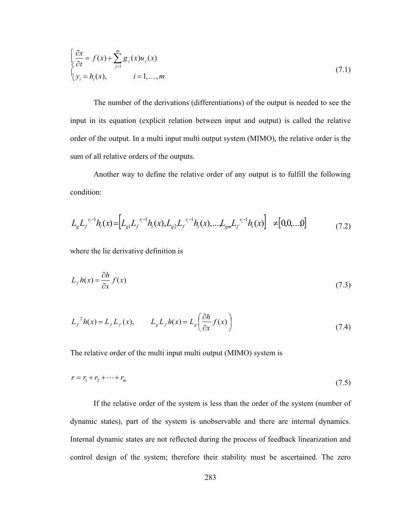
283
mixhy
xuxgxft
x
ii
m
jjj
,,1),(
)()()(1
(7.1)
The number of the derivations (differentiations) of the output is needed to see the
input in its equation (explicit relation between input and output) is called the relative
order of the output. In a multi input multi output system (MIMO), the relative order is the
sum of all relative orders of the outputs.
Another way to define the relative order of any output is to fulfill the following
condition:
0,...,0,0)(),...,(),()( 112
11
1 xhLLxhLLxhLLxhLL ir
fgmir
fgir
fgir
fgiiii (7.2)
where the lie derivative definition is
)()( xfx
hxhL f
(7.3)
)()(),()(2 xfx
hLxhLLxLLxhL gfgfff
(7.4)
The relative order of the multi input multi output (MIMO) system is
mrrrr 21 (7.5)
If the relative order of the system is less than the order of the system (number of
dynamic states), part of the system is unobservable and there are internal dynamics.
Internal dynamic states are not reflected during the process of feedback linearization and
control design of the system; therefore their stability must be ascertained. The zero

284
dynamics is a special case of the internal dynamics and are defined to be the internal
dynamics of the system when the selected system outputs are set to zero by the input.
There are two methods to isolate the zero dynamics [140-141].
7.2.1 First Method
In the first method [140] for finding the zero dynamics, after defining the number
of internal dynamics (n–∑ri), all the outputs should be made equal to zero. In this case
some dynamic states will be removed, leaving the internal dynamics which are
independent of the input variables.
It should be noted that if the purpose for checking the stability of the zero
dynamics is to use the input/output linearization method for the controller design we
define the characteristic matrix as
mr
fgmmr
fg
rfgm
rfg
h
hLLhLL
hLLhLL
xCmm 11
1
11
11
111
)(
(7.6)
Non-singularity of the characteristic matrix in a MIMO system is a sufficient
condition for input/output linearization to be achievable through static state feedback. For
systems for which this condition is not satisfied, controllers with dynamic contents can be
employed to transform them to new equations satisfying the characteristic matrix [138].

285
7.2.2 Second Method
In the second method based on [141], a new co-ordinate system with )(xt is
generated in which the elements of the following matrix are linearly independent:
)(
)(
)(
)(
)(
)(
)(
)(
1
11
1
1
1
1
0
1
xhL
xhL
xh
xhL
xhL
xh
xt
xt
mr
f
mf
m
rf
f
rn
m
m
i
(7.7)
The original dynamic equations of the system are now converted to the new
coordinates in which the input variables have been eliminated. For a MIMO system the
following can be defined:
mixhLW
mixhLLxhLLC
rnitLtLG
rnixtLF
ir
fi
ir
fgmir
fgi
m
iiigmigi
m
iiifi
i
ii
,,1)(
,,1)()(
)(,,1
)(,,1)(
111
11
1
(7.8)

286
2sR 2sLasI 2
bsI 2
csI 2
dcVdcC
asV 2
bsV 2
csV 2
saV
sbV
scV
1I 2IsaI
sbI
scI
gaV
gbV
gcV
Figure 7.1 Schematic diagram of IPM wind turbine connected to the main grid with L type filter.
The zero dynamics after converting the matrices to the new coordinates (the
output variables will be either zero or at their steady state values) are defined as follows:
m
m
rnrn
rnWW
C
C
GFdt
d
ii
i 1
1
1)0(
(7.9)
7.3 Controllability of Wind Turbine Connected through L filter to the Grid
As illustrated in Figure 7.1, in the study system, an interior permanent magnet
generator driven by a wind turbine supplies power to the grid. A back to back AC/DC/AC
inverter converts the AC generator output voltage to a DC voltage and then to another
three-phase AC voltage. The grid side inverter is interfaced to the grid through the L type
filter.
In the interior permanent magnet machine, the dynamic of the rotor can be
neglected because the permanent magnet is a poor electrical conductor. Ignoring the core

287
Table 7.1 Parameters of the IPM machine for controllability analysis
ratedmV 180 V ratedmI 5.5 A
ratedrm 1800 rpm P (no of poles) 4
sR 1.5 Ω m 0.21 Wb
sdL 0.035 H sqL 0.11 H
dcC 600e-6 F J 0.089 kg/m2
gqV 170 V gdV 0 V
2sR 0.01 Ω 2sL 0.4 mH
loss of the machine the dynamic equations of the generator are as follows:
mrsdsdrsqsqsqssqdc
q ILpILIRVV
M 21
(7.10)
sqsqrsdsdsdssddc
d ILpILIRVV
M 21
(7.11)
The converter DC Capacitor equation is given as
21121 )(4
3IIMIMIIpVC sddsqqdcdc
(7.12)
where sqdV , sqdI are the complex qd-axis voltages and currents of the stator. 1qdM and
dcV are the complex qd-axis modulation index of machine side converter and DC link
voltage respectively. sR is the stator resistance. sqdL and m are qd-axis stator
inductance and

288
magnetization flux of the generator.
The dynamic equations of the main grid with L type filter and grid side converter
are
dsseqssqssgqdcq ILpILIRVV
M222222
2
2 (7.13)
qssedssdssgddcd ILpILIRVV
M222222
2
2
(7.14)
Parameters of the IPM machine and the grid are presented in Table 7.1. For generator
copper loss minimization the following requirement should be met [125]
0),(
sdsq
sd
loss
sq
loss
sd
e
sq
e
IIf
I
P
I
PI
T
I
T
(7.15)
sdmssdsqsdssqsqsds IRILLRILLRP
22 )()(
4
9 (7.16)
7.3.1 Steady State and Stable Operation Region
Under steady state operating conditions the derivatives of the states in (7.10) to
(7.14) are set to zero. The resulting equations with the algebraic equation defining the
reference grid reactive power and the condition for minimum generator loss (7.16) are
used to determine the steady state operation. The known variables are
dctrggdgq VTQVV )( (7.17)
289
And the unknown variables are
222211 dqdsqsdqsdsq MMIIMMII (7.18)
The rotor speed and the DC capacitor voltage are varied ( r and dcV ) to solve the steady-
state equations given as
0))(2
3(
0)()(4
9
0))((4
3
0)(4
3)(
4
3
02
02
02
02
22
22
222211
22222
22222
1
1
qsgddsgqg
sdmssdsqsdssqsqsds
sdsqsqsdsqmt
dsdqsqsddsqq
qssedssgddc
d
dsseqssgqdc
q
sqsqrsdsdc
d
mrsdsdrsqsdc
q
IVIVQ
IRILLRILLRP
IILLIP
T
IMIMIMIM
ILIRVV
M
ILIRVV
M
ILIRV
M
ILIRV
M
(7.19)
The steady state operation regions of the generator system are illustrated in Figure
7.2. In this figure the output active and reactive power of the IPM generator are shown.
The stator current and voltage of the machine are presented in parts Figure 7.2b and
Figure 7.2c respectively. The steady state parameters of the machine are just related to
the input wind power or rotor speed which is directly related to it with MPP algorithm.
The modulation index of the machine side converter is related to both rotor speed and DC
link voltage and it is always in the linear region below unity. Because all the power

290
300 300
600 600900 900
1200
A) Vdc
wr
(rad
/s)
Ps
400 500 600 700 800 900150200250300350
-1500-1200
-900-600-300
B) Vdc
wr
(rad
/s)
Qs
400 500 600 700 800 900150200250300350
1 5 1 5
3 3
4.5 4.5
6 6
C) Vdc
wr
(rad
/s)
Is
400 500 600 700 800 900150200250300350
40 40
80 80120 120160 160
200
D) Vdc
wr
(rad
/s)
Vs
400 500 600 700 800 900150200250300350
0 15
0.150.3
0.30.45
0.45
0.60.75
E) Vdc
wr
(rad
/s)
M1
400 500 600 700 800 900150200250300350
04
0.50.
60.7
0 .8
0 .9
F) Vdc
wr
(rad
/s)
M2
400 500 600 700 800 900150200250300350
Figure 7.2 Steady state operation region of the system. a) output active power of the generator (W), b) output reactive power of the generator (Var), c) stator current (A), d)
stator voltage (V), e) modulation index magnitude of machine side converter f) modulation index magnitude of grid side converter
coming from the wind on the other side is transmitting to the grid and the voltage of the
grid is constant, the modulation index of the grid side converter in Figure 7.2 is just
related to the DC link voltage magnitude.
To study the stability region of the system in all feasible operation regions, the
model equations of the electrical subsystem is linearized and its characteristic equation is
defined as a sixth order equation

291
sqsdsqsdsdsqsqsdsqmr
dsdqsqsddsqqdc
dc
qssedssdc
ds
ds
dsseqssdc
qs
qs
rsqsqsqsqrsdsdc
dsd
sd
mrrsdsdsdsdrsqsdc
qsq
sq
IILLIILLIJ
pp
IMIMIMIMC
Vp
ILIRV
ML
Ip
ILIRV
ML
Ip
ILILIRV
ML
Ip
ILILIRV
ML
Ip
00
2
222211
222222
2
222222
2
001
001
)()(8
3
4
3
2
1
2
1
2
1
2
1
(7.20)
r
dc
ds
qs
sd
sq
sqsqsdsdsqsdm
dc
d
dc
q
dc
d
dc
q
s
d
s
se
s
qe
s
s
sd
sqsq
sd
d
sd
s
sd
sqr
sq
msdsd
sq
q
sq
sdr
sq
s
r
dc
ds
qs
sd
sq
V
I
I
I
I
J
ILLp
J
ILLpC
M
C
M
C
M
C
ML
M
L
RL
M
L
RL
IL
L
M
L
R
L
LL
IL
L
M
L
L
L
R
p
Vp
Ip
Ip
Ip
Ip
2
2
02
02
2211
2
2
2
2
2
2
2
2
010
010
2
2
00008
)(3
8
)(3
004
3
4
3
4
3
4
3
02
00
02
00
200
200
(7.21)
0012
23
34
45
56
6 aaaaaaaAI (7.22)
The coefficients of (7.22) are presented in Appendix A. Using the Routh–Hurwitz criteria
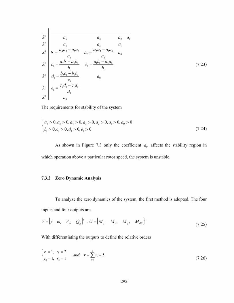
292
00
1
01121
1
01
21121
2
1
05112
1
25131
3
05
61522
5
63541
4
1355
02466
ad
acdce
ac
cbcbd
b
aabac
b
babac
aa
aaaab
a
aaaab
aaa
aaaa
(7.23)
The requirements for stability of the system
0,0,0,0
0,0,0,0,0,0,0
1111
0123456
edcb
aaaaaaa
(7.24)
As shown in Figure 7.3 only the coefficient 0a affects the stability region in
which operation above a particular rotor speed, the system is unstable.
7.3.2 Zero Dynamic Analysis
To analyze the zero dynamics of the system, the first method is adopted. The four
inputs and four outputs are
Tgdcr QVY , Tdqdq MMMMU 2211 (7.25)
With differentiating the outputs to define the relative orders
51,1
2,1 4
143
21
i
irrandrr
rr
(7.26)
293
0 0 0 0
Vdc
wr
(rad
/s)
a0
400 500 600 700 800 900100
150
200
250
300
350
Unstable Region
Stable Region
Figure 7.3 Stability region based on Routh–Hurwitz criteria. The last coefficient of the characteristic equation.
Therefore the system has one (n–∑ri) internal dynamic. The zero dynamics is obtained
when all the output variables are set to zero. With the grid voltage taken as the reference
for the qd synchronous reference frame transformation and aligning the grid voltage in
the q-axis )0,( gdggq VVV
sdmssdsqsdssqsqsds
dcrqsgddsgqg
sdsqsqsdsqmtr
dsdqsqsddsqqdcdc
IRILLRILLRP
VIVIVQ
IILLIP
Tp
IMIMIMIMpVC
22
22
222211
)()(4
90
0,0),(2
30
))((4
30
)(4
3)(
4
30
(7.27)
then
1
1
q
sddsq M
IMI (7.28)
and the only remaining dynamic, the zero dynamic of the system, is
0 sdsdsds pILIR (7.29)
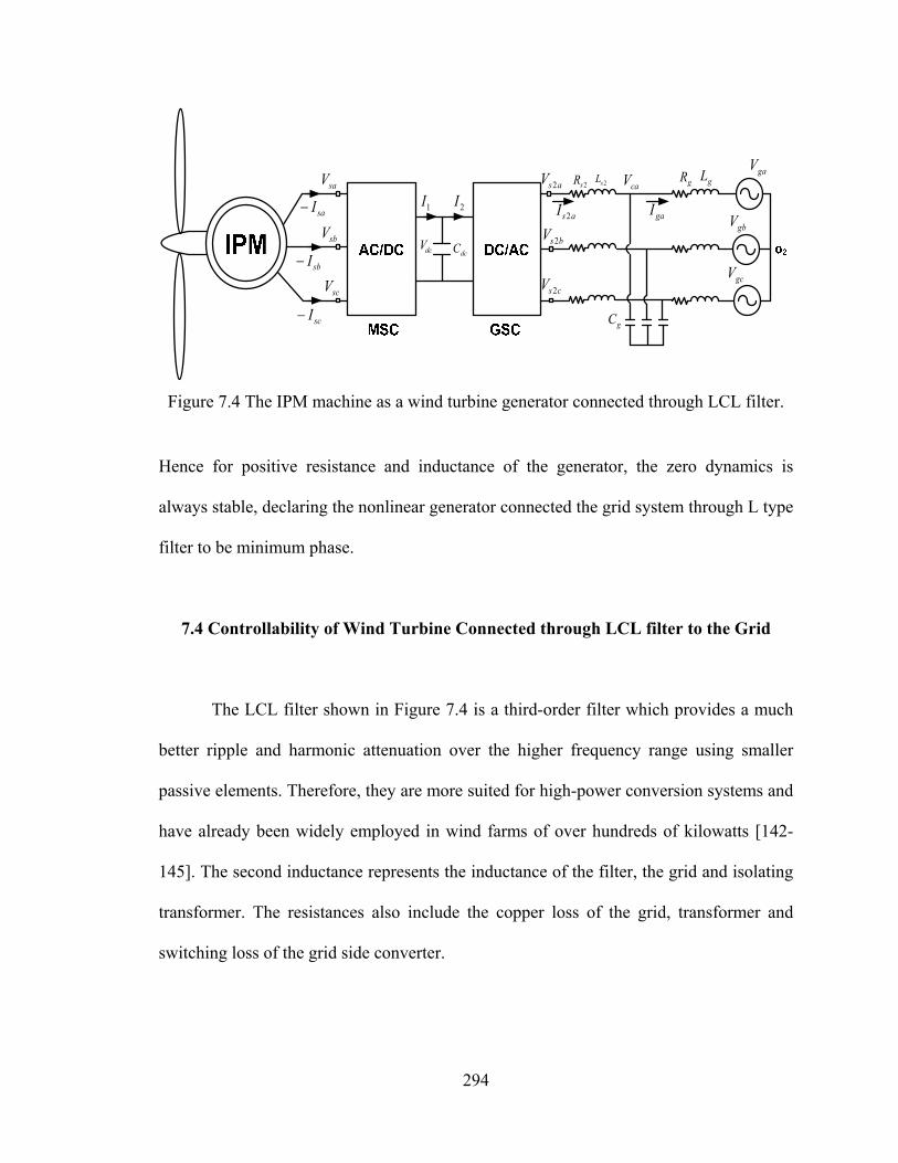
294
2sR 2sL
asI 2
dcVdcC
asV 2
bsV 2
csV 2
saV
sbV
scV
1I 2IsaI
sbI
scI
gaV
gbV
gcV
gC
gLgR
gaI
caV
Figure 7.4 The IPM machine as a wind turbine generator connected through LCL filter.
Hence for positive resistance and inductance of the generator, the zero dynamics is
always stable, declaring the nonlinear generator connected the grid system through L type
filter to be minimum phase.
7.4 Controllability of Wind Turbine Connected through LCL filter to the Grid
The LCL filter shown in Figure 7.4 is a third-order filter which provides a much
better ripple and harmonic attenuation over the higher frequency range using smaller
passive elements. Therefore, they are more suited for high-power conversion systems and
have already been widely employed in wind farms of over hundreds of kilowatts [142-
145]. The second inductance represents the inductance of the filter, the grid and isolating
transformer. The resistances also include the copper loss of the grid, transformer and
switching loss of the grid side converter.

295
7.4.1 Steady State and Stable Operation Region
The total dynamic equations of the system with the LCL filter are
))((4
3
222
)(4
3)(
4
3
)(1
)(1
2
2
2
2
22221121
2
2
2222222
2222222
1
1
sdsqsqsdsqmtetr
dsdqsqsddsqqdcdc
cqgegddsg
cd
cdgegqqsg
cq
gqgegdggdggdcd
gdgegqggqggqcq
qssedssdsscddc
d
dsseqssqsscqdc
q
sqsqrsdsdsdsdc
d
mrsdsdrsqsqsqsdc
q
IILLIP
J
pT
J
pTT
J
pp
IMIMIMIMIIpVC
VCIIC
pV
VCIIC
pV
ILpILIRVV
ILpILIRVV
ILpILIRVV
M
ILpILIRVV
M
ILpILIRV
M
ILpILIRV
M
(7.30)
In steady state the derivative parts are zero so we can solve eight equations
including six dynamic equations in steady state condition along with the two algebraic
equations of reactive power and loss minimization. Therefore there are
The known variables
dctrgdgq VTQVV )(2 (7.31)
The unknown variables

296
400600
600
800
800
800
1000
1000
1000
1200
1200
1200
1400
1400
1400
1600
1600
1600
1800
1800
1800
2000
2000
20002200
2200
2200
2400
2400
2400
2600
2600
26002800
280030003200
Vdc
wr
(rad
/s)
Ps
400 500 600 700 800 900
50
100
150
200
250
300
350
Figure 7.5 Output active power of IPM generator.
-3900
-3600
-3300
-3300-3000
-3000
-3000-2700
-2700
-2700
-2400
-2400
-2400
-2100
-2100
-2100
-1800
-1800
-1800
-1500
-1500
-1500
-1200
-1200
-1200
-900
-900
-900
-600-600
Vdc
wr
(rad
/s)
Qs
400 500 600 700 800 900
50
100
150
200
250
300
350
Figure 7.6 Output reactive power of IPM generator.
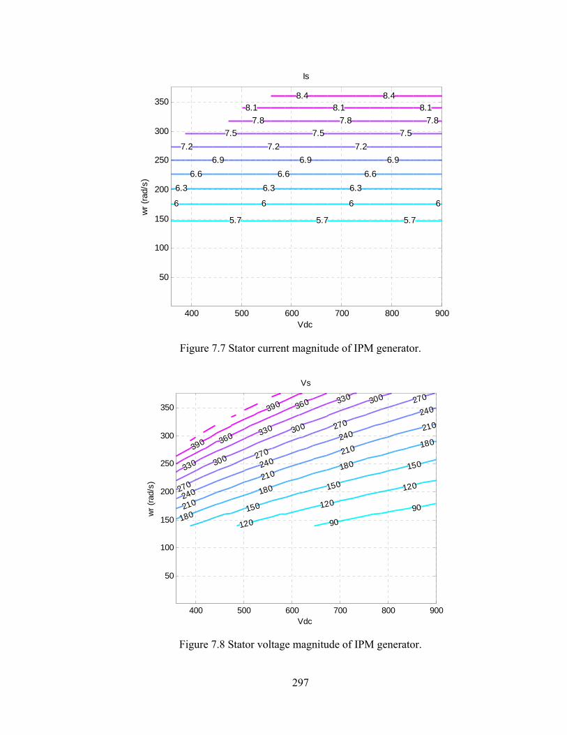
297
5.7 5.7 5.7
6 6 6 6
6.3 6.3 6.3
6.6 6.6 6.6
6.9 6.9 6.9
7.2 7.2 7.2
7.5 7.5 7.5
7.8 7.8 7.8
8.1 8.1 8.18.4 8.4
Vdc
wr
(rad
/s)
Is
400 500 600 700 800 900
50
100
150
200
250
300
350
Figure 7.7 Stator current magnitude of IPM generator.
90
90
120
120
120
150
150
150
180
180
180
180
210
210
210
210
240
240
240
240270
270
270
270
300
300
300
330
330
330
360
360390
390
Vdc
wr
(rad
/s)
Vs
400 500 600 700 800 900
50
100
150
200
250
300
350
Figure 7.8 Stator voltage magnitude of IPM generator.

298
0.2
0.2
0.3
0.3
0.3
0.4
0.4
0.4
0.4
0.5
0.5
0.5
0.5
0.6
0.6
0.6
0.6
0.7
0.7
0.7
0.8
0.80.9
0.9
0.9
Vdc
wr
(rad
/s)
M1
400 500 600 700 800 900
50
100
150
200
250
300
350
Figure 7.9 Modulation index magnitude of the machine side inverter.
0 .4
0 .4
0 .4 5
0 .4 5
0 .5
0 .5
0.55
0.55
0.6
0.6
0.65
0.65
0.7
0.7
0.7 50.8
0.85
0.9
Vdc
wr
(rad
/s)
M2
400 500 600 700 800 900
50
100
150
200
250
300
350
Figure 7.10 Modulation index magnitude of the grid side inverter.

299
400 400 400
600 600 600
800 800 800
1000 1000 1000
1200 1200 1200
1400 1400 1400
1600 1600 16001800 1800
2000 2000
Vdc
wr
(rad
/s)
Pg
400 500 600 700 800 900
50
100
150
200
250
300
350
Figure 7.11 Active power flowing into the grid.
cdcqgdgqdqdsqsdqsdsq VVIIMMIIMMII 222211 (7.32)
So we can vary r and dcV to calculate the other twelve variables. The results are
illustrated in Figure 7.5 to Figure 7.11.
We can study the stability region of this system using the small signal analysis in
any steady state point. We can define the eigenvalues of the system in that point and
check for stability.
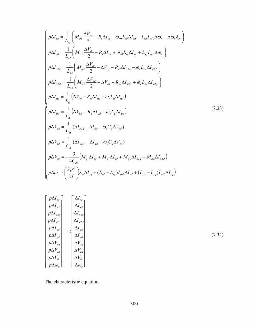
300
sqsdsqsdsdsqsqsdsqmr
dsdqsqsddsqqdc
dc
cqgegddsg
cd
cdgegqqsg
cq
gqgegdgcdg
gd
gdgegqgcqg
gq
qssedsscddc
ds
ds
dsseqsscqdc
qs
qs
rsqsqsqsqrsdsdc
dsd
sd
mrrsdsdsdsdrsqsdc
qsq
sq
IILLIILLIJ
pp
IMIMIMIMC
Vp
VCIIC
Vp
VCIIC
Vp
ILIRVL
Ip
ILIRVL
Ip
ILIRVV
ML
Ip
ILIRVV
ML
Ip
ILILIRV
ML
Ip
ILILIRV
ML
Ip
00
2
222211
2
2
222222
2
222222
2
001
001
)()(8
3
4
3
)(1
)(1
1
1
2
1
2
1
2
1
2
1
(7.33)
r
dc
cd
cq
gd
gq
ds
qs
sd
sq
r
dc
cd
cq
gd
gq
ds
qs
sd
sq
V
V
V
I
I
I
I
I
I
A
p
Vp
Vp
Vp
Ip
Ip
Ip
Ip
Ip
Ip
2
2
2
2
(7.34)
The characteristic equation

301
0012
23
34
45
56
67
78
89
910
10 aaaaaaaaaaaAI (7.35)
Using the Routh–Hurwitz criteria we can check for stability. Because all eigenvalues in
all operation regions are negative, the system is always stable.
7.4.2 Zero Dynamic Analysis
The dynamic equation of the system with the LCL filter in the nonlinear format
44332211)( ugugugugxfX (7.36)
Where
))((8
3
2
0
)(
211
2
764
853
568
657
2
32
2
42
2
8
2
42
2
32
2
7
1102
102101
xxLLxJ
PT
J
p
C
xC
C
x
C
x
C
xC
C
x
C
x
L
xL
L
xR
L
V
L
x
L
xL
L
xR
L
V
L
xL
xL
L
xR
L
xL
xL
L
xR
L
xL
xLx
L
xR
L
x
L
xLx
L
xR
xf
sqsdmt
g
ge
gg
g
ge
gg
g
ge
g
g
g
gd
g
g
ge
g
g
g
gq
g
s
se
s
s
s
s
se
s
s
s
sd
sq
sd
s
sq
m
sq
sd
sq
s
(7.37)

302
04
30
0
0
02
0
0
0
)(,
04
30
0
0
0
02
0
0
)(,
04
30
0
0
0
0
02
0
)(,
04
30
0
0
0
0
0
02
)(
4
2
9
4
3
2
9
3
2
9
2
1
9
1
dc
s
dc
s
dc
sd
dc
sq
C
x
L
x
xg
C
x
L
x
xg
C
x
L
x
xg
C
x
L
x
xg
(7.38)
The Output equations
)(2
3
)()(4
9
)(
)(
)(
)(
56
9
10
22
22
1
4
3
2
1
xVxV
x
x
xRxLLRxLLRP
xh
xh
xh
xh
Y
gdgq
mssqsdssqsds
(7.39)
Where
rdccdcqgdgqdsqssdsq VVVIIIIIIX 22 (7.40)
The new states and inputs are
2211 dqdq MMMMU (7.41)
With the same output variables in the new ten order system with LCL filter defined in
(7.39) the relative orders defined as
73,1
2,1 4
143
21
i
irrandrr
rr
(7.42)

303
Therefore there are three (n–∑ri) internal dynamics. In this system, the second
method has been use for defining the zero dynamics. In the first step, based on (7.7), the
new coordinates of the system are
g
gd
g
ggqgegd
g
gq
g
gegqggd
g
ggqgegd
g
gegqggd
g
ggqggegd
g
gegqggegd
gg
gq
g
ggegqgegd
g
ggegqggd
gg
gd
gg
gq
gg
gd
g
gq
g
gd
g
ggqgegd
g
gegqggd
gdgq
sqsdmt
mssqsdssqsds
m
L
V
L
RVLV
L
V
L
LVRVx
L
RVLV
xL
LVRVx
L
RVRLV
L
LVRLV
CL
V
xL
RLVLV
L
RLVRV
CL
Vx
CL
Vx
CL
V
xL
Vx
L
Vx
L
RVLVx
L
LVRV
xVxV
x
xxLLxJ
PT
J
p
x
xRxLLRxLLRP
xt
xt
xt
2
3
2
32
2
3
2
2
3
2
3
2
3
2
3
2
3
2
3
2
3
2
3
2
3
)(2
3
))((8
3
2
)()(4
9)(
)(
)(
82
7262
2
2
22
52
22
2
2
43
8765
56
9
211
210
22
22
1
3
2
1
1
0
(7.43)
55857565554535
84746454
5363
9
221212
10
212
212
11
3
2
1
43
42
41
31
22
21
11
03
02
01
1
0
)(
)(
)(
jixhxexdxcxbxa
xdxcxbxa
xbxa
x
cxxbxa
x
xcxbxa
xt
xt
xt
m
(7.44)
where t(x) is chosen as
334251 )(,)(,)( xxtxxtxxt (7.45)

304
With )(xt given in (7.45), the linearized matrix of will be
0000
000000
00000000
0100000000
00000000
1000000000
0000000022
0000000100
0000001000
0000010000
555555
4444
33
12222
12111
1
0
hedcba
dcba
ab
xbxba
cxbxa
oo
oo
m
(7.46)
In which the determinant of the linearized matrix )(x is not equal to zero
02
9
0)det(
3
22
g
gegqgegd4554
345542o212122
2o122o112
1o2
L
LVLVde-hc
)ade-h)(cxbc-ac-bx2b-ax2b-ax-(2b
(7.47)
Therefore all elements of the matrix are linearly independent. The system equations in the
new coordinates are given as
21
31
84
34
24
10
30
20
18
74
34
24
10
30
20
17
41
016
01
02
03
22
112
22
111
10
9
8
7
6
5
4
3
2
1
),,,,,(
),,,,,(
),(
),(
),(
xx
xx
x
x
x
Cf
Cf
f
f
f
x
x
x
x
x
x
x
x
x
x
(7.48)

305
The zero dynamics are determined by setting the output variables to either zero or the
steady-state values
ref
refdc
refr
ss
Qxh
Vxh
xh
xh
_24
14
_3
13
_2
12
111
)(
)(
)(
0)(
(7.49)
and their derivatives
0
0
0
43
42
22
(7.50)
With equation (7.50), the new equations are given in (7.51) which are constant.
22
11
x
x
ax
ax
(7.51)
Using (7.8) the following can be calculated
2
42
2
32
2
733
2
32
2
42
2
822
65711
s
se
s
s
sf
s
se
s
s
sf
g
ge
g
g
g
gq
gf
L
xL
L
xR
L
xtLF
L
xL
L
xR
L
xtLF
L
xL
L
xR
L
V
L
xtLF
(7.52)
The other matrices are defines as

306
02
00
2000
0000
2
9343332313
2
9242322212
141312111
sgggg
sgggg
gggg
L
xtLtLtLtLG
L
xtLtLtLtLG
tLtLtLtLG
(7.53)
To substitute the input variables with the states, we need to define the equations of
)(xC and )(xW as
92
92
4
43213
91
92
2
2
92
911
4
3
4
300
4
3
002
)(2
))((8
3
002
)(22
)(4
9
xLCL
Vx
LCL
VC
xxxxC
C
L
xxLL
L
xxLL
J
PC
L
xRxLLR
L
xxLLR
PC
sgg
gq
sgg
gd
dc
sdsqsd
sqsqsdm
sdmssqsds
sqsqsds
(7.54)
81571561551541531541
31
11021
10210122
21
110222
1021011
11
0
)(
)(
8
3
)(2
)(2
4
9
fhfefdfcfbfaW
W
L
xLx
L
xRxLL
L
x
L
xLx
L
xRxLL
J
PW
L
xLx
L
xRRxLLR
L
x
L
xLx
L
xRxLLR
PW
sd
sq
sd
ssqsd
sq
m
sq
sd
sq
ssqsdm
sd
sq
sd
smssqsds
sq
m
sq
sd
sq
ssqsds
(7.55)
The above equations are transformed to the new coordinates to yield the equations
of the zero dynamics given below:
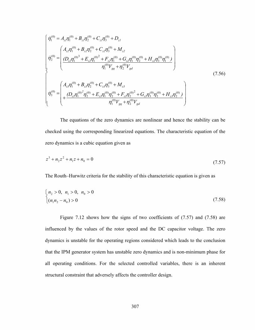
307
gdgq
z3z3z3z3
2
z3
z3z3z3z3
gdgq
z2z2z2z2z2
z2z2z2z2
z1z1z1z1
VV
)HGFE(D
MCBA
VV
)HGFE(D
MCBA
DCBA
)0(2
)0(1
)0(2
)0(2
)0(3
2)0(2
)0(2
)0(1
)0(2
)0(1
)0(3
)0(2
)0(1
)0(3
)0(2
)0(1
)0(1
)0(3
)0(2
)0(1
)0(1
2)0(1
3)0(1
)0(3
)0(2
)0(1
)0(2
)0(3
)0(2
)0(1
)0(1
(7.56)
The equations of the zero dynamics are nonlinear and hence the stability can be
checked using the corresponding linearized equations. The characteristic equation of the
zero dynamics is a cubic equation given as
0012
23 nznznz
(7.57)
The Routh–Hurwitz criteria for the stability of this characteristic equation is given as
0)(
0,0,0
021
012
nnn
nnn
(7.58)
Figure 7.12 shows how the signs of two coefficients of (7.57) and (7.58) are
influenced by the values of the rotor speed and the DC capacitor voltage. The zero
dynamics is unstable for the operating regions considered which leads to the conclusion
that the IPM generator system has unstable zero dynamics and is non-minimum phase for
all operating conditions. For the selected controlled variables, there is an inherent
structural constraint that adversely affects the controller design.
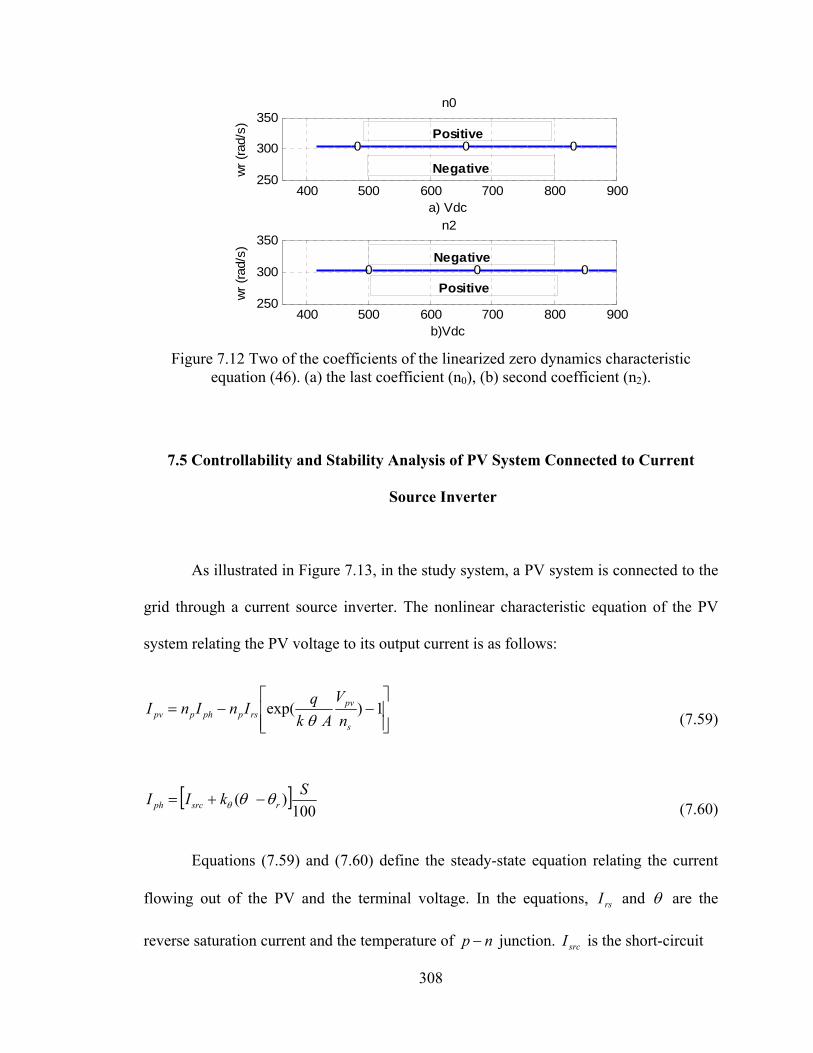
308
0 0 0
a) Vdc
wr
(rad
/s)
n0
400 500 600 700 800 900250
300
350
0 0 0
b)Vdc
wr
(rad
/s)
n2
400 500 600 700 800 900250
300
350
Positive
Negative
Negative
Positive
Figure 7.12 Two of the coefficients of the linearized zero dynamics characteristic equation (46). (a) the last coefficient (n0), (b) second coefficient (n2).
7.5 Controllability and Stability Analysis of PV System Connected to Current
Source Inverter
As illustrated in Figure 7.13, in the study system, a PV system is connected to the
grid through a current source inverter. The nonlinear characteristic equation of the PV
system relating the PV voltage to its output current is as follows:
1)exp(
s
pvrspphppv n
V
Ak
qInInI
(7.59)
100
)(S
kII rsrcph (7.60)
Equations (7.59) and (7.60) define the steady-state equation relating the current
flowing out of the PV and the terminal voltage. In the equations, rsI and are the
reverse saturation current and the temperature of np junction. srcI is the short-circuit

309
asI 1
1cV
1dI
gaV
gbV
gcV
mC
gLgR
gaI
maV
1dR 1dL
dcV1C
pvI
Figure 7.13 An IPM machine as a wind turbine generator connected through LCL filter.
current of one PV cell, sn and pn are the number of series and parallel PV cells in a
string, respectively. A is the ideality factor and S is solar irradiation level. r is the cell
reference temperature and k is the temperature coefficient. )602.1( 19Ceq and
)/38.1( 23 KJek are the unit electric charge and Boltzmann’s constant. Table I shows
parameters of PV system. The dynamic equations of the grid is
gqgegdggdggdmd
gdgegqggqggqmq
ILpILIRVV
ILpILIRVV
(7.61)
where gqdV and gqdI are the qd-axis grid voltage and current. The inverter and DC side
dynamic equations are as follows:
mddmqqdc
dd
ds
dq
qs
VMVMV
IM
I
IM
I
4
32
2
11
11
(7.62)

310
mqmemdmgddd
mdmemqmgqdq
VCpVCIIM
VCpVCIIM
1
1
2
2 (7.63)
11111 4
3ddddmddmqqc pILIRVMVMV
(7.64)
111 dpvc IIpVC and pvc VV 1 (7.65)
To control the input current of the inverter and the reactive power following into
the grid
gqgdgdgqg
mddd
mqdq
dddddd
IVIVQ
VIM
VIM
IVpILIR
2
3
222
3
2
11111
211
211
(7.66)
If we align the grid voltage to the q-axis reference frame ( 0gdV ) and operate the system
under unity power factor
02
3 gdgqg IVQ
(7.67)
7.5.1 Steady State and Stability Analysis of the System
Under steady state operating conditions the derivatives of the states are set to
zero. The resulting equations with the algebraic equation defining the reference grid

311
reactive power and operating under maximum power point of PV are used to determine
the steady state operation. The known variables are
pvpvggdgq VIQVV (7.68)
And the unknown variables are
1dmdmqgdgqdq IVVIIMM (7.69)
The irradiation of the sun is varied ( 1S ) and the PV voltage and current based on
maximum power point operation arte calculated to solve the steady-state equations given
as
02
3
0
04
3
02
02
0
0
1
111
1
1
gdgqg
dpv
ddmddmqqd
mqmegddd
mdmegqdq
gqgegdggdmd
gdgegqggqmq
IVQ
II
IRVMVMV
VCIIM
VCIIM
ILIRVV
ILIRVV
(7.70)
To study the stability region of the system in all feasible operation regions, the
model equations of the electrical subsystem are linearized. The output, input and state
variables of the system
g
d
Q
Ixh
21)( ,
d
q
M
MU , pvdgdgqmdmq VIIIVVX 1
(7.71)
To define the number of internal dynamics

312
111
111
1
11
11
1)exp(
4
3
4
3
4
3
4
31
22
1
22
1
1
1
dpvs
pv
s
rsppv
dddmdo
mddo
qmqo
mqqo
pvd
d
mqmegddod
ddo
mmd
mdmegqqod
dq
mmq
gqgegdgmdg
gd
gdgegqgmqg
gq
IC
Vn
V
Ak
q
AnkC
IqnVp
IRMV
VM
MV
VM
VL
Ip
VCIMI
IM
CVp
VCIMI
IM
CVp
ILIRVL
Ip
ILIRVL
Ip
o
(7.72)
)exp(1
0000
1
4
3
4
300
02
01
0
02
001
001
0
0001
11
11
1
11
s
pv
s
rsp
dd
d
d
do
d
qo
m
doe
m
m
qoe
m
gg
ge
ge
g
g
n
V
Ak
q
AnkC
Iqn
C
LL
R
L
M
L
MC
M
C
C
M
C
LL
RLL
R
A
(7.73)
The characteristic equation is defined as a sixth order equation
0012
23
34
45
56
6 aaaaaaaAI (7.74)
The coefficients of (7.74) are presented in Appendix B. Using the Routh–Hurwitz, the
criteria for stability is as
0,0,0,0
0,0,0,0,0,0,0
1111
0123456
edcb
aaaaaaa
(7.75)
The parameters of (7.75) are defined using (7.23).

313
0.4 0.5 0.6 0.7 0.8 0.9 11070
1080
1090
1100
1110
1120
1130
S1 (irradiation level)
Vpv
MPP
(V
)
0.4 0.5 0.6 0.7 0.8 0.9 1600
700
800
900
1000
1100
1200
1300
1400
S1 (irradiation level)
Id1=
Ipv M
PP (
A
Figure 7.14 PV output voltage at MPP with in different irradiation level
Figure 7.15 PV output current at MPP with in different irradiation level
0.4 0.5 0.6 0.7 0.8 0.9 10.75
0.8
0.85
0.9
0.95
1
S1 (irradiation level)
M
0.4 0.5 0.6 0.7 0.8 0.9 12000.2
2000.25
2000.3
2000.35
2000.4
2000.45
2000.5
S1 (irradiation level)
Vm
q (V
)
Figure 7.16 Inverter modulation index magnitude at different irradiation level
Figure 7.17 q-axis capacitor voltage at different irradiation level
After applying the steady state parameters, the system is stable in the whole operation
region.
7.5.2 Zero Dynamics Analysis of PV
To analyze the zero dynamics of the system the two inputs and two outputs are
314
Tgd QIxh 21)( , Tdq MMU (7.76)
Differentiate the outputs to define the relative orders the results are
3,2
,1 2
12
1
i
irrandr
r (7.77)
Therefore the system has three (n–∑ri) internal dynamics.
The dynamic equations of the system in nonlinear format are as
2211 )()()( uxguxgxfX (7.78)
2
1
4
51
1
3
5
1
5
1
51
1
1
6
32
41
124
213
6
5
4
3
2
1
04
32
0
0
0
04
30
2
0
0
u
L
xC
xu
L
x
C
x
C
x
C
I
xL
R
L
x
xC
x
xC
x
xxL
R
L
x
xxL
R
L
V
L
x
x
x
x
x
x
x
d
m
d
m
pv
d
d
d
em
em
eg
g
g
eg
g
g
gq
g
(7.79)
2
25
2
1
2
3)(
)(
xV
x
xh
xhY
gq
(7.80)
The new coordinates of the system are

315
124
2
25
3
2
1
1
0
2
32
3
)(
)(
)(
xxL
R
L
xV
xV
x
xt
xt
xt
eg
g
ggq
gqm
(7.81)
If we choose
633211 )(,)(,)( xxtxxtxxt (7.82)
6
5
4
3
2
1
5
1
0
002
30
2
3
2
3
00002
30
020000
100000
000100
000001
x
x
x
x
x
x
L
V
L
RVV
V
x
g
gq
g
ggqegq
gq
o
m
(7.83)
02
9)det( 5
2
og
gq xL
V
(7.84)
With )(xt given in (7.82), the determinant of the linearized matrix )(x is not
equal to zero, in which case all the elements of )(x are linearly independent. The
system equations in the new coordinates are given as

316
03
11
21
01
22
02
21
01
6
5
4
3
2
1
3
2
3
2
3
2
gq
gge
gq
g
gq
V
RL
V
L
V
x
x
x
x
x
x
(7.85)
The following can be calculated
1
5
133
41
22
213
11
C
x
C
ItLF
xC
xtLF
xxL
R
L
V
L
xtLF
pvf
em
f
eg
g
g
gq
gf
(7.86)
The other matrices are defines as
00
02
00
32313
522212
12111
tLtLG
C
xtLtLG
tLtLG
gg
mgg
gg
(7.87)
To substitute the input variables with the states we need to define the equations of
)(xC and )(xW as
gm
gqfgfg
ddgg
LC
xVhLLhLLC
L
xx
L
xxhLhLC
4
30
2
3
2
3
522212
1
45
1
3512111
(7.88)
317
32
124
213
22
31
124
221
25
1
1
1
65111
2
3
2
3
2
3
2
3
22
xC
x
L
Vxx
L
R
L
x
L
RV
xxL
R
L
V
L
xV
hLW
xxL
R
L
xVhLW
xL
R
L
xxhLW
emg
gqe
g
g
gg
ggq
eg
g
g
gq
g
egq
f
eg
g
g
gqf
d
d
df
(7.89)
For calculation of zero dynamics, we should put outputs either zero or as their
steady state value. Thus their derivative will be zero. Therefore
0)(
)(2
2_2
11
2_1
111
refg
refd
Qxh
Ixh
(7.90)
From the above results, during the calculation of zero dynamics we can consider
cteIax
cteV
Qax
refdx
gq
refgx
_155
_22 3
2
(7.91)
and there is no need for their conversion to new coordinates.

318
03
5
_01
02
2
01
6
5
4
3
2
1
3
2
x
gq
refggge
x
aV
QRL
a
x
x
x
x
x
x
(7.92)
If we convert the matrices iF , iG , iC , iW to new coordinates
1
5
133
_01
20
122
20
1
02
11
3
2
C
a
C
ItLF
V
QRL
CtLF
aL
R
L
V
LtLF
xpvf
gq
refggege
mf
xeg
g
g
gq
gf
(7.93)
00
02
00
32313
522212
12111
tLtLG
C
atLtLG
tLtLG
gg
m
xgg
gg
(7.94)
gm
xgqfgfg
gq
refggge
d
x
d
xgg
LC
aVhLLhLLC
V
QRL
L
a
L
ahLhLC
4
30
3
2
2
3
2
3
522212
_01
1
5
1
025
12111
(7.95)

319
012
_01
02
22
01
02
22
21
25
1
1
1
035
111
3
2
2
3
2
3
2
3
22
exg
g
g
gq
refggge
g
ggq
em
x
g
gqxe
g
g
g
gq
g
egq
f
xd
d
d
xf
aL
R
L
V
QRL
L
RV
C
a
L
Va
L
R
L
V
L
V
hLW
aL
R
L
ahLW
(7.96)
1
_1
1
03
02
0326
02
0125
02
20124
02
23012221
02
_01
020
1 3
2
C
I
C
I
aaaaaa
V
Q
L
R
L
V
L
refdpv
gq
refge
g
g
g
gq
g
(7.97)
310
3
02
0326
02
0125
02
20124
02
23012221
02
0213
011211
01
a
aaaaaa
aaa
(7.98)
03
02
01
02
260326
0125
201242320
2
02
250
12422
1312
03
02
01
000
120
aaaaa
aaa
aa
(7.99)
012 bsbssASI
(7.100)
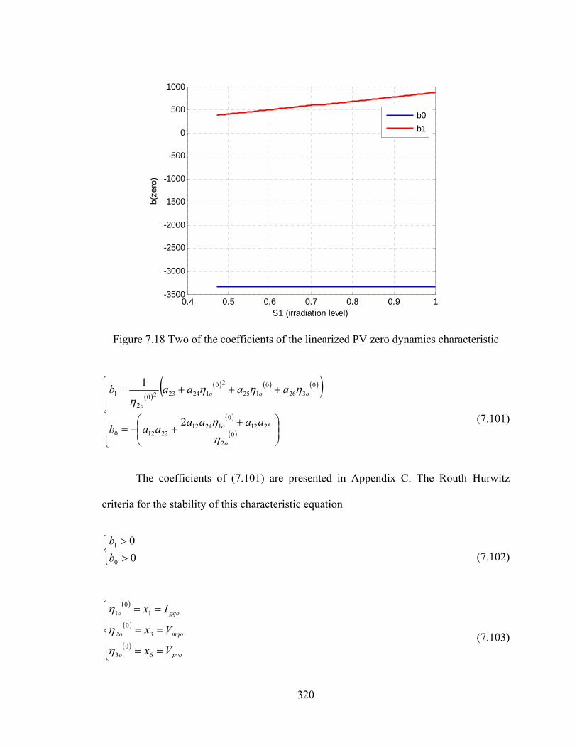
320
0.4 0.5 0.6 0.7 0.8 0.9 1-3500
-3000
-2500
-2000
-1500
-1000
-500
0
500
1000
S1 (irradiation level)
b(ze
ro)
b0
b1
Figure 7.18 Two of the coefficients of the linearized PV zero dynamics characteristic
02
25120
1241222120
0326
0125
201242320
2
1
2
1
o
o
ooo
o
aaaaaab
aaaab
(7.101)
The coefficients of (7.101) are presented in Appendix C. The Routh–Hurwitz
criteria for the stability of this characteristic equation
0
0
0
1
b
b
(7.102)
pvoo
mqoo
gqoo
Vx
Vx
Ix
60
3
30
2
10
1
(7.103)

321
Therefore besides one of the characteristic equation poles at origin ( 0S ),
second coefficient of Routh–Hurwitz criteria ( 0b ) in all operating region is negative. It
means the PV system connected to the current source inverter is non-minimum phase in
its all operation region.
7.6 Conclusions
This chapter investigated the controllability analysis of the wind turbine driven
interior permanent magnet (IPM) generator interfaced to the grid using either an L or
LCL filter. The stability regions of the operation based on maximum power point
tracking of the wind turbine and loss minimization of the generator were shown. With the
aid of two methods used for the extraction of the zero dynamics, it was shown that the
generator fitted with the L filter has a stable zero dynamics, possesses a minimum phase
characteristics which ensures that no structural limitation is imposed on the design of the
controllers. When the generator is grid-interfaced using the LCL filter, the zero dynamics
is unstable for all operating points, and in the small, the system is non-minimum phase.
There is a structural constraint (such as limited current regulator bandwidth and response
time) on any controller to be designed for the system. Also, the nonlinear controller
design using the method of feedback state linearization cannot be applied to the control of
the four specified variables of the IPM generator with LCL filter. Modest dynamic
performance can however be achieved by using higher order controllers and/or high gain
observers.

322
The controllability analysis for the IPM generator system suggests that the
topological structure of the interface filter and the controlled variables have significant
effects on the phase behavior of the system, the agility of any controller used, and hence
the static and dynamic performance of the controlled generator system. This chapter
provides an explanation as to why designing controllers for renewable energy systems
with LCL interfaces with the grid has continued to be a challenge. Appropriate selection
of controlled variables, states to be estimated using high gain observers and using high
order controllers point the way for designing controllers that will deliver good static and
dynamic performance.

323
CHAPTER 8
8.CONCLUSION AND FUTURE WORKS
8.1 Introduction
The previous works that have been done related to this area are detailed in chapter
1. The conclusions and contributions of this dissertation are summarized in this chapter.
A short summary of each section is presented to discuss the proposed topics and
approaches of this dissertation and the overall point of view is explained. Future works
are also discussed.
8.2 Conclusions
State space modeling, stability analysis and dynamic behavior of a small
Microgrid in both autonomous mode and grid connected mode are presented. The main
objective of this investigation is to improve the control of Microgrid for both autonomous
and grid conned modes. The droop control is applied to the maintain voltage and
frequency. Frequency droops against output active power of converter while voltage
magnitude droops against reactive power. The PI load voltage control and inner current
control of the system are designed based on the dynamic equations in complex form.
Along with considering both modes of operation, the locally available control parameters
of each DG unit are used, so that communication among DG units is avoided in order to
improve the system reliability and reduce the costs. The three phase PLL is designed and

324
added to each converter in order to measure instantaneous local frequency used for the
qd-axis transformation. The system is simulated using MATLAB software to validate the
design. The controllers share the power based on the related power for different sources
with different rated power and different impedance connections to the network.
Instead of a constant DC source for the input of the inverter, in this dissertation a
photovoltaic source with its nonlinear characteristic is used. The DG unit is connected to
the main grid through the three phase inverter. The load voltage magnitude and frequency
are adapted from the main grid. The DC link voltage is controlled for maximum power
point operation of the PV. For unity power factor operation the second reference has been
considered as output reactive power of the three phase inverter. With the change of
irradiation level, DC link voltage and reactive power controllers follow their references
precisely. Even during sudden change of the loads, the actual parameters of the system
are still tracking their references well due to the fast response of the controllers. The DG
unit is always operating in unity power factor and the modulation indices of the inverter
even during transients are less than unity.
In autonomous operation of the microgrid, due to the limitation of the DG power
for feeding the loads is included. A battery with a bidirectional DC-DC converter is
added. Simulation results show that the battery discharges when total load is more than
the maximum power of PV system. Under a lower irradiation level, the maximum power
of PV system decreases, thus the battery discharges even under reduced load demand.
When the inverter modulation index magnitude is reduced while keeping the load voltage
constant, the input DC link voltage and the duty ratios of the two boost converters
interfacing the sources are increased.

325
To verify the proposed controllers, the laboratory scale experiment is implemented in
addition to the dynamic simulation of the system. The designed experimental system consists of
a microgrid with two different sources, a nonlinear PV source and a battery source. A
programmable DC source is used to emulate the nonlinear PV source characteristic. Three
different power electronic converters, a unidirectional DC-DC boost converter, a bidirectional
buck and boost converter and a three phase inverter are built. Each converter has its own
controller signals coming from different control structures, drivers, sensor boards and digital
signal processor (DSP) unit. The process of the design and test of each section are explained
in detail. All the controllers, analog to digital conversions and PWM signal generation are
implemented inside the ezDSPF28335. The maximum power point tracking of the PV
source, active and reactive power control of the three phase inverter and charging and
discharging control of the battery are applied. The experimental results are presented in
both autonomous mode and grid connected mode after synchronization and connection of
the system to the main network.
Along with the programmed PLL, the enhanced phase lock loop (EPLL) also is
designed and the experimental results of both systems are compared. EPLL is used to
define the reference frequency and angle of the load voltage. It is operated as a band pass
filter for the other parameters such as the inverter and the grid currents. EPLL results
have the lowest noise and therefore it tracks the magnitudes, angles and frequencies of
the actual input signals more precisely.
Wind energy, as one of the most popular renewable sources in Microgrid, is also
studied. In the interior permanent magnet structure, the equivalent air gap is not uniform
and it makes the saliency effect obvious. In the IPM machine, both magnetic and
reluctance torque can be produced. Compared to the surface mounted permanent magnet

326
(SPM) machine, the IPM machine has a mechanically robust and solid structure since the
magnets are physically contained and protected. It contains both reluctance and magnetic
torque which increases the efficiency and speed range operation. In this dissertation the
dynamic model of interior permanent magnet machine as a wind turbine generator is
studied. An AC-DC-AC converter connects the wind turbine to the main grid. The steady
state operation regime of IPM generator in wind turbine application based on total loss
minimization and maximum power point tracking of the wind turbine is presented. The
proposed controllers in dynamic operation are designed to get maximum power from the
wind, keep DC link voltage constant and guarantee unity power factor operation. At
higher than rated wind speeds the reference of the active power and rotor speed are kept
constant and pitch angle controlled to protect the wind turbine from over speed and over
current phenomenon.
Finally, the controllability analysis of the wind turbine driven interior permanent
magnet (IPM) generator interfaced to the grid using either an L or LCL filter is presented.
The stability regions of its operation based on maximum power point tracking of the wind
turbine and loss minimization of the generator are analyzed. With the aid of two methods
used for the extraction of the zero dynamics, it is shown that the generator fitted with the
L filter has a stable zero dynamics, possesses a minimum phase characteristics which
ensures that no structural limitation is imposed on the design of the controllers. When the
generator is grid-interfaced using the LCL filter, the zero dynamics is unstable for all
operating points and the system is non-minimum phase. There are structural constraints
(such as limited current regulator bandwidth and response time) on any controller to be
designed for the system. Also, the nonlinear controller design using the method of

327
feedback state linearization cannot be applied to the control of the IPM generator with
LCL filter. Modest dynamic performance can however be achieved by using higher order
controllers and/or high gain observers.
8.3 Future Work
The concept of microgrid and renewable energies is relatively new compared to
conventional power plants. In this dissertation, the two most popular renewable sources
including photovoltaic (PV) and wind energy are studied. The structure of the PV system
in both grid connected and autonomous operation are both simulated and verified
experimentally. Some future work that can be done is to experimentally validate the
proposed topologies for the interior permanent magnet machine based wind turbine.
The programmable source is used as a PV source. This system is not very
accurate and due to the needed time for communication between the hardware DC source
and the computer, it sometimes loses the tracking and behaves like a normal voltage
source. Therefore the designed setup can be connected to a real PV solar cell array to test
the maximum power point tracking.
The operation of a two DG unit system is investigated and the proposed controller
for sharing the load can be applied to multi DG unit systems. Due to hardware limitations
such as the number of the ports on the DSP, this work could not be extended. Almost
ninety percent of the analog to digital conversion ports and pwm ports are used. So using
a more powerful DSP or combination of FPGA and DSP can extend the system to a
multi-DG unit with different types of sources.

328
Most electrical power systems are nonlinear and complex. The explained
controllability analysis is a useful methodology that can be applied to other structures to
study their characteristics and have an overall point of view about their responses without
linearization which is what relates the analysis to the selected operation point. It will also
help in the design process of the controllers.

329
REFERENCES

330
[1] T. C. Green and M. Prodanovic´, “Control of inverter-based microgrids,” Journal of
Elect. Power Syst. Research, vol. 77, no. 9, pp. 1204–1213, Jul. 2007.
[2] J. M. Guerrero, J. C. Vasquez, J. Matas, M. Castilla and L.G.Vicuna, “Control Strategy
for Flexible Microgrid Based on Parallel Line-Interactive UPS Systems” IEEE Trans. on
Industrial Electronics, Vol. 56, Issue 3, pp. 726 – 736, March 2009.
[3] F. Katiraei and M. R. Iravani, “Power Management Strategies for a Microgrid with
Multiple Distributed Generation Units” IEEE Trans. on Power Systems, Vol. 21, Issue 4,
pp. 1821 – 1831, Nov. 2006.
[4] C. K. Sao and P. W. Lehn, “Control and Power Management of Converter Fed
Microgrids” IEEE Trans. on Power Systems, Vol. 23, Issue 3, pp. 1088 – 1098, Aug.
2008.
[5] J. C. Vasquez, J. M. Guerrero, A. Luna, P. Rodriguez and R.Teodorescu, “Adaptive
Droop Control Applied to Voltage-Source Inverters Operating in Grid-Connected and
Islanded Modes” IEEE Trans. on Industrial Electronics, Vol. 56, Issue 10, pp. 4088 –
4096, Oct. 2009.
[6] M. C. Chandorkar, D. M. Divan, and R. Adapa, “Control of parallel connected inverters
in standalone ac supply systems,” IEEE Trans. Ind. Appl., vol. 29, no. 1, pp. 136–143,
Jan./Feb. 1993.
[7] J. Holtz and K.-H. Werner, “Multi-inverter UPS system with redundant load sharing
control,” IEEE Trans. Ind. Electron., vol. 37, no. 6, pp. 506–513, Dec. 1990.
[8] J.-F. Chen and C.-L. Chu, “Combination voltage controlled and
currentcontrolledPWMinverters for UPS parallel operation,” IEEE Trans. Power
Electron., vol. 10, no. 5, pp. 547–558, Sep. 1995.
[9] H. Van Der Broeck and U. Boeke, “A simple method for parallel operation of inverters,”
in Proc. IEEE Telecommunications Energy Conference, 1998, pp. 143–150.
[10] T. Kawabata and S. Higashino, “Parallel operation of voltage source inverters,” IEEE
Trans. Ind. Appl., vol. 24, no. 2, pp. 281–287, Mar./Apr. 1988.
[11] H. Hanaoka, “Development of a novel parallel redundant UPS,” in Proc. IEEE
Telecommunications Energy Conference, 2003, pp. 493–498.
[12] M. C. Chandorkar, D. M. Divan, Y. Hu, and B. Banerjee, “Novel architecture and control
for distributed UPS systems,” in Proc. IEEE APEC, 1994, pp. 683–689.

331
[13] M. Arias, D. G. Lamar, M. Rodriguez, M. Hernando, and A. Fernandez, “Simple droop
voltage control system for parallel operation of UPS,” in Proc. IEEE APEC, 2004, pp.
1946–1951.
[14] W. Yao, M. Chen, J. Chen, and Z. Qian, “An improved multiple-loop controller for
parallel operation of single-phase inverters with no control interconnections,” in Proc.
IEEE PESC, 2007, pp. 448–452.
[15] K. De Brabandere, B. Bolsens, J. Van den Keybus, A. Woyte, J. Driesen, and R. A.
Belmans, “Voltage and frequency droop control method for parallel inverters,” IEEE
Trans. Power Electron., vol. 22, no. 4, pp. 1107–1115, Jul. 2007.
[16] Y. W. Li and C. Kao, “An accurate power control strategy for power electronics
interfaced distributed generation units operating in a low voltage multibus microgrid,”
IEEE Trans. Power Electron., vol. 24, no. 12, pp. 2977–2988, Dec. 2009.
[17] L. Mihalache, “Paralleling control technique with no intercommunication signals for
resonant controller-based inverters,” in Conf. Rec. IEEE IAS Annu. Meeting, 2003, vol. 3,
pp. 1882–1889.
[18] U. Borup, F. Blaabjerg, and P. N. Enjeti, “Sharing of nonlinear load in parallel-connected
three-phase converters,” IEEE Trans. Ind. Appl., vol. 37, no. 6, pp. 1817–1823,
Nov./Dec. 2001.
[19] S. J. Chiang and J. M. Chang, “Parallel control of the UPS inverters with frequency-
dependent droop scheme,” in Proc. IEEE PESC, 2001, pp. 957–961.
[20] K. Jaehong, J.M. Guerrero, P. Rodriguez, R. Teodorescu and N. Kwanghee, “Mode
Adaptive Droop Control With Virtual Output Impedances for an Inverter-Based Flexible
AC Microgrid,” IEEE Trans. on Power Electronics, vol.26, no.3, pp.689-701, March
2011.
[21] C. Trujillo, F. Velasco, D. G. Garcera, E. Figueres and J.Guacaneme, “Reconfigurable
control scheme for a PV microinverter working in both grid connected and island modes”
IEEE Trans. on Industrial Electronics, 2012.
[22] S. V. Iyer, M. N. Belur and M. C. Chandorkar, “Analysis and Mitigation of Voltage
Offsets in Multi-inverter Microgrids” IEEE Trans. on Energy Conversion, Vol. 26, Issue
1, pp. 354 – 363, March 2011.
332
[23] J. C. Vasquez, R. A. Mastromauro, J. M. Guerrero and M. Liserre, “Voltage Support
Provided by a Droop-Controlled Multifunctional Inverter” IEEE Trans. on Industrial
Electronics, Vol. 56, Issue 11, pp. 4510 – 4519, Nov. 2009.
[24] C. Chen, Y. Wang, J. Lai, Y. Lee and D. Martin, “Design of Parallel Inverters for Smooth
Mode Transfer Microgrid Applications” IEEE Trans. on Power Electronics, Vol. 25,
Issue 1, pp. 6 – 15, Jan. 2010.
[25] A. Tuladhar, H. Jin, T. Unger, and K. Mauch, “Control of parallel inverters in distributed
ac pouver systems with consideration of the line impedance tifect,” in Proc. APEC, vol.
1, Feb. 1998, pp. 321–328.
[26] C. K. Sao and P. W. Lehn, “Autonomous Load Sharing of Voltage Source Converters”
IEEE Trans. on Power Delivery, Vol. 20, Issue 2, pp. 1009 – 1016, April 2005.
[27] R. Majumder, B. Chaudhuri, A. Ghosh, R. Majumder, G. Ledwich and F. Zare,
“Improvement of Stability and Load Sharing in an Autonomous Microgrid Using
Supplementary Droop Control Loop” IEEE Trans. on Power Systems, Vol. 25, Issue 2,
pp. 796 – 808, May 2010.
[28] R. Majumder, A. Ghosh, G. Ledwich and F.Zare, “Power Management and Power Flow
Control with Back-to-Back Converters in a Utility Connected Microgrid” IEEE Trans. on
Power Systems, Vol. 25, Issue 2, pp. 821 – 834, May 2010.
[29] R. Majumder, A. Ghosh, G. Ledwich and F.Zare, “Angle Droop versus Frequency Droop
in a Voltage Source Converter Based Autonomous Microgrid” In Proc. of Power &
Energy Society General Meeting, pp.1 – 8, 2009.
[30] J. M. Guerrero, L. G. Vicuna, J. Matas, M. Castilla, and J. Miret, “Output impedance
design of parallel-connected UPS inverters with wireless load-sharing control,” IEEE
Trans. Ind. Electron., vol. 52, pp. 1126–1135, Aug. 2005.
[31] J. M. Guerrero, J. Matas, L. G. Vicuna, M. Castilla, and J. Miret, “Decentralized control
for parallel operation of distributed generation inverters using resistive output
impedance,” IEEE Trans. Ind. Electron., vol. 54, pp. 994–1004, Apr. 2007.
[32] F. Blaabjerg, Z. Chen, and S. B. Kjaer, “Power electronics as efficient interface in
dispersed power generation systems,” IEEE Trans. Power Electron., vol. 19, pp. 1184–
1194, Sep. 2004.

333
[33] R. Majumder,.A. Ghosh, G. Ledwich and F. Zare, “Load sharing and power quality
enhanced operation of a distributed microgrid,” IET Renewable Power Generation., vol.
3, no. 2, pp. 109–119, June 2009.
[34] A. Engler, “Applicability of droops in low voltage grids,” DER Journal, vol. 1, pp. 1-5,
Jan. 2005.
[35] J. M. Guerrero, L. G. Vicuna, J. Matas, M. Castilla, and J. Miret, “A wireless controller
to enhance dynamic performance of parallel inverters in distributed generation systems,”
IEEE Trans. Power. Electron., vol. 19, no. 5, pp. 1205–1213, Sep. 2004.
[36] Y. Li and Y. W. Li, “Power Management of Inverter Interfaced Autonomous Microgrid
Based on Virtual Frequency-Voltage Frame” IEEE Trans. on Smart Grid, Vol. 2, Issue
1, pp.30 – 40, March 2011.
[37] Y. Li and Y. W. Li, “Decoupled power control for an inverter based low voltage
microgrid in autonomous operation,” in Proc. IEEE IPEMC, 2009, pp. 2490–2496.
[38] D. De and V.Ramanarayanan, “Decentralized Parallel Operation of Inverters Sharing
Unbalanced and Non-linear Loads” IEEE Trans. on Power Electronics, Vol. 25, Issue
12, pp. 3015 – 3025, Dec. 2010.
[39] E. Rokrok and M. E. H. Golshan, “Adaptive voltage droop scheme for voltage source
converters in an islanded multibus microgrid” IET Generation, Transmission &
Distribution, Vol. 4, Issue 5, pp. 562 – 578, March 2010.
[40] S. Yang, Q. Lei, F. Z. Peng and Z. Qian, “A Robust Control Scheme for Grid-Connected
Voltage-Source Inverters” IEEE Trans. on Industrial Electronics, Vol. 58, Issue 1, pp.
202 – 212, Jan. 2011
[41] M. Vidyasagar, “Optimal rejection of persistent bounded disturbances,” IEEE Trans.
Autom. Control, vol. AC-31, no. 6, pp. 527–534, Jun. 1986.
[42] W. M. Haddad and V. Chellaboina, “Mixed-norm H2/L1 controller synthesis via fixed-
order dynamic compensation: A Riccati equation approach,” in Proc. 36th Conf. Decision
Control, Dec. 1997, pp. 452–457.
[43] V. S. Chellaboina, W. M. Haddad, and J. H. Oh, “Fixed-order dynamic compensation for
linear systems with actuator amplitude and rate saturation constraints,” International
Journal of Control, vol. 73, no. 12, pp. 1087–1103, Aug. 2000.

334
[44] I. Y. Chung, W. Liu, D. A. Cartes, E. G. Collins and S. Moon, “Control Methods of
Inverter-Interfaced Distributed Generators in a Microgrid System” IEEE Trans. on
Industry Applications, Vol. 46, Issue 3, pp. 1078 – 1088, May 2010.
[45] R. C. Dugan, M. F. McGranaghan, and H. W. Beaty, Electrical Power Systems Quality.
New York: McGraw-Hill, 2002.
[46] Y. W. Li, D. M. Vilathgamuwa and P. C. Loh, “Robust Control Scheme for a Microgrid
With PFC Capacitor Connected” IEEE Trans. on Industry Applications, Vol. 43, Issue 5,
pp. 1172 – 1182, Sept. 2007.
[47] M. A. Hassan and M. A. Abido, “Optimal Design of Microgrids in Autonomous and
Grid-Connected Modes Using Particle Swarm Optimization” IEEE Trans. on Power
Electronics, Vol. 26, Issue 3, pp. 755 – 769, March 2011.
[48] N. Pogaku, M. Prodanovic and T. C. Green, “Modeling, Analysis and Testing of
Autonomous Operation of an Inverter-Based Microgrid” IEEE Trans. on Power
Electronics, Vol. 22, Issue 2, pp. 613 – 625, March 2007.
[49] E. Barklund, N. Pogaku, M. Prodanovic, C. Aramburo, and T. Green, “Energy
management in autonomous microgrid using stability-constrained droop control of
inverters,” IEEE Trans. Power Electron., vol. 23, no. 5, pp. 2346–2352, Sep. 2008.
[50] Y. Mohamed and E. Saadany, “Adaptive decentralized droop controller to preserve
power sharing stability of paralleled inverters in distributed generation microgrids,” IEEE
Trans. Power Electron., vol. 23, no. 6, pp. 2806–2816, Nov. 2008.
[51] S.V. Iyer, M. N. Belur and M. C. Chandorkar, “A Generalized Computational Method to
Determine Stability of a Multi-inverter Microgrid” IEEE Trans. on Power Electronics,
Vol. 25, Issue 9, pp. 2420 – 2432, Sept. 2010.
[52] M. Z. Kamh and R.Iravani, “Unbalanced Model and Power-Flow Analysis of Microgrids
and Active Distribution Systems” IEEE Trans. on Power Delivery, Vol. 25, Issue 4,
pp.2851 – 2858, Oct. 2010.
[53] M. Illindala and G. Venkataramanan, “Control of distributed generation systems to
mitigate load and line imbalances,” in Proc. 33rd Annu. IEEE PESC, 2002, pp. 2013–
2018.
[54] P. Hsu and M. Behnke, “A three-phase synchronous frame controller for unbalanced
load,” in Proc. 29th Annu. IEEE PESC, 1998, pp. 1369–1374.
335
[55] Y. Li, D. M. Vilathgamuwa, and L. P. Chiang, “Microgrid power quality enhancement
using a three-phase four-wire grid-interfacing compensator,” IEEE Trans. Ind. Appl., vol.
41, no. 6, pp. 1707–1719, Nov./Dec. 2005.
[56] H. S. Song and K. H. Nam, “Dual current control scheme for PWM converter under
unbalanced input voltage conditions,” IEEE Trans. Ind. Electron., vol. 46, no. 5, pp. 953–
959, Oct. 1999.
[57] W. C. Lee, T. K. Lee, and D. S. Hyun, “A three-phase parallel active power filter
operating with PCC voltage compensation with consideration for an unbalanced load,”
IEEE Trans. Power Electron., vol. 17, no. 5, pp. 807– 814, Sep. 2002.
[58] Y. Li, D. M. Vilathgamuwa, and P. C. Loh, “A grid-interfacing power quality
compensator for three-phase three-wire Microgrid applications,” IEEE Trans. Power
Electron., vol. 21, no. 4, pp. 1021- 1031, Jul. 2006.
[59] M. Hojo, Y. Iwase, T. Funabashi, and Y. Ueda, “A method of three phase balancing in
microgrid by photovoltaic generation systems,” in Proc. Power Electron. and Motion
Cont. Conf. (EPE-PEMC), pp. 2487-2491, Sept. 2008.
[60] P. T. Cheng, C. Chen, T. L. Lee, and S. Y. Kuo, “A cooperative imbalance compensation
method for distributed-generation interface converters,” IEEE Trans. Ind. Appl., vol. 45,
no. 2, pp. 805-815, Mar./Apr. 2009.
[61] S. A. O. Da Silva, P. F. D. Garcia, P. C. Cortizo, and P. F. Seixas, “A three-phase line-
interactive UPS system implementation with seriesparallel active power-line conditioning
capabilities,” IEEE Trans. Ind. Appl., vol. 38, no. 6, pp. 1581-1590, Nov./Dec. 2002.
[62] P. Pillay, and M. Manyage, “Definitions of voltage unbalance,” IEEE Power Eng.
Review, vol. 21, no. 5, pp. 49-51, May. 2001.
[63] E. Barklund, N. Pogaku, M. Prodanovic´, C. H. Aramburo, and T. C. Green, “Energy
management in autonomous microgrid using stability-constrained droop control of
inverters,” IEEE Trans. Power Electron., vol. 23, no. 5, pp. 2346-2352, Sept. 2008.
[64] J. M. Guerrero, J. C. Vasquez, J. Matas, L. G. de Vicuña, and M. Castilla, “Hierarchical
control of droop-controlled AC and DC microgrids—a general approach toward
standardization,” IEEE Trans. Ind. Electron., vol. 58, no. 1, pp. 158-172, Jan. 2011.

336
[65] M. Savaghebi, A. Jalilian, J. C. Vasquez and J. M.Guerrero, “Secondary Control Scheme
for Voltage Unbalance Compensation in an Islanded Droop-Controlled Microgrid” IEEE
Trans. on Smart Grid, , pp. 1 – 11, 2012.
[66] M. Savaghebi, A. Jalilian, J. Vasquez and J. Guerrero, “Autonomous Voltage Unbalance
Compensation in an Islanded Droop-Controlled Microgrid” IEEE Trans. on Industrial
Electronics, 2012.
[67] A. Mehrizi-Sani and R. Iravani, “Potential-Function Based Control of a Microgrid in
Islanded and Grid-Connected Modes” IEEE Trans. on Power Systems, Vol. 25, Issue 4,
pp.1883 – 1891, Nov. 2010.
[68] I. J. Balaguer, U.Supatti,; L. Qin, C. Nam-Sup and F. Z. Peng, “Intelligent control for
intentional islanding operation of microgrids” In Proc. of Sustainable Energy
Technologies Conference, Vol. 24, Issue 1, pp. 898 – 903, 2008.
[69] I. J. Balaguer, U.Supatti,; L. Qin, C. Nam-Sup and F. Z. Peng, “Control for Grid-
Connected and Intentional Islanding Operations of Distributed Power Generation” IEEE
Trans. on Industrial Electronics, Vol. 58, Issue 1, pp.147 – 157, Jan. 2011.
[70] X. Q. Guo and W.Y.Wu, “Improved current regulation of three-phase grid-connected
voltage-source inverters for distributed generation systems” IET Renewable Power
Generation, Vol. 4, Issue 2, pp.101 – 115, 2010.
[71] Z. Lidong, L. Harnefors and H. P. Nee, “Power-Synchronization Control of Grid-
Connected Voltage-Source Converters” IEEE Trans. on Power Systems, Vol. 25, Issue 2,
pp. 809 – 820, May 2010.
[72] Z. Lidong, L. Harnefors and H. P. Nee, “Interconnection of Two Very Weak AC Systems
by VSC-HVDC Links Using Power-Synchronization Control” IEEE Trans. on Power
Systems, Vol. 26, Issue 1, pp. 344 – 355, Feb. 2011.
[73] M. Popov, H. Karimi, H. Nikkhajoei and V. Terzija, “Dynamic Model and Control of a
Microgrid with Passive Loads” International Conference on Power Systems Transients,
June 2009.
[74] H. Karimi, H. Nikkhajoei, R. Iravani, “Control of an Electronically-Coupled Distributed
Resource Unit Subsequent to an Islanding Event” IEEE Trans. on Power Delivery, Vol.
23, Issue 1, pp. 493 - 501, Jan. 2008.
337
[75] Q. Lei, S. Yang and F. Z. Peng, “Multi-loop control algorithms for seamless transition of
grid-connected inverter” In Proc. of Applied Power Electronics Conference and
Exposition, pp. 844 – 848, 2010.
[76] O. Wasynczuk, “Dynamic behavior of a class of photovoltaic power systems,” IEEE
Trans. Power App. Syst., vol. PAS-102, no. 9, pp. 3031–3037, Sep. 1983.
[77] N. Femia, G. Petrone, G. Spagnuolo, and M. Vitelli, “A technique for improving P&O
MPPT performances of double-stage grid-connected photovoltaic systems,” IEEE Trans.
Ind. Electron., vol. 56, no. 11, pp. 4473–4482, Nov. 2009.
[78] R. Alonso, P. Ibáñez, V. Martinez, E. Román, and A. Sanz, “An innovative perturb,
observe and check algorithm for partially shaded PV systems,” In proc. Power
Electronics and Applications Conf., Spain, 2009, pp. 1-8.
[79] W. T. Chee, T. C. Green, and A. H.-A. Carlos, “Analysis of perturb and observe
maximum power point tracking algorithm for photovoltaic applications,” In Proc. Power
and Energy Conf., Malaysia, 2008, pp. 237-242.
[80] C. W. Tan, T. C. Green, and C. A. Hernandez-Aramburo, “A current mode controlled
maximum power point tracking converter for building integrated photovoltaics,” In Proc.
Power Electronics and Applications Conf., Denmark, 2007, pp. 1-10.
[81] A. Pandey, N. Dasgupta, and A. K. Mukerjee, “High-performance algorithms for drift
avoidance and fast tracking in solar MPPT system,” IEEE Trans. Energy Convers., vol.
23, no. 2, pp. 681–689, Jun. 2008.
[82] E. Koutroulis, K. Kalaitzakis, and N. C. Voulgaris, “Development of a microcontroller-
based, photovoltaic maximum power point tracking control system,” IEEE Trans. Power
Electron., vol. 16, no. 1, pp. 46–54, Jan. 2001.
[83] M. A. Elgendy, B. Zahawi and D. J. Atkinson, “Assessment of Perturb and Observe
MPPT Algorithm Implementation Techniques for PV Pumping Applications” IEEE
Trans. on Sustainable Energy, Vol. 3, Issue 1, pp. 21 – 33, Jan. 2012.
[84] A. K. Abdelsalam, A. M. Massoud, S. Ahmed and P. N. Enjeti, “High-Performance
Adaptive Perturb and Observe MPPT Technique for Photovoltaic-Based Microgrids”
IEEE Trans. on Power Electronics, Vol. 26, Issue 4, pp. 1010 – 1021, April 2011.

338
[85] N. Femia, G. Petrone, G. Spagnuolo and M. Vitelli, “Optimization of Perturb and
Observe Maximum Power Point Tracking Method” IEEE Trans. on Power Electronics,
Vol. 20, Issue 4, pp. 963 – 973, July 2005.
[86] E. Koutroulis and F. Blaabjerg, “A New Technique for Tracking the Global Maximum
Power Point of PV Arrays Operating Under Partial-Shading Conditions” IEEE Journal of
http://ieeexplore.ieee.org/xpl/RecentIssue.jsp?punumber=5503869 Photovoltaics, Vol. 2,
Issue 2, pp. 184 – 190, 2012.
[87] G. Adinolfi, N. Femia, G. Petrone, G. Spagnuolo and M. Vitelli, “Design of dc/dc
Converters for DMPPT PV Applications Based on the Concept of Energetic Efficiency”
Journal of Solar Energy Engineering, Vol. 132, pp.1 – 10, May 2010.
[88] G. Petrone, G. Spagnuolo, R. Teodorescu, M. Veerachary and M.Vitelli, “Reliability
Issues in Photovoltaic Power Processing Systems” IEEE Trans. on Industrial Electronics,
Vol. 55, Issue 7, pp. 2569 – 2580, July 2008.
[89] S. B. Kjaer, J. K. Pedersen, and F. Blaabjerg, “A review of single-phase grid-connected
inverters for photovoltaic modules,” IEEE Trans. Ind. Appl., vol. 41, no. 5, pp. 1292–
1306, Sep./Oct. 2005.
[90] Q. Li and P. Wolfs, “A review of the single phase photovoltaic module integrated
converter topologies with three different DC link configurations,” IEEE Trans. Power
Electron., vol. 23, no. 3, pp. 1320–1333, May 2008.
[91] E. Ozdemir and F. Kavaslar, “A new multifunctional power converter for grid connected
residential photovoltaic applications,” In Proc. IEEE Energy Conversion Congress and
Exposition, Sep. 2009, pp. 2650–2656.
[92] L. Ma, K. Sun, R. Teodorescu, J. M. Guerrero, and X. Jin, “An integrated multifunction
DC/DC converter for PV generation systems,” In Proc. IEEE Int. Symp. Industrial
Electronics, 2010, pp. 2205–2210.
[93] Y. Gurkaynak and A. Khaligh, “Control and power management of a grid connected
residential photovoltaic system with plug-in hybrid electric vehicle (PHEV) load,” In
Proc. IEEE Appl. Power Electron. Conf., 2009, pp. 2086–2091.
[94] G. M. Tina and F. Pappalardo, “Grid-connected photovoltaic system with battery storage
system into market perspective,” In Proc. IEEE Power and Energy Society/Industry
Application Society Conf., Sep. 2009, pp. 1–7.

339
[95] T. Shimada, Y. Ueda, and K. Kurokawa, “Look-ahead equalizing charge planning for
grid-connected photovoltaic systems with battery storages,” In Proc. IEEE Photovoltaic
Spec. Conf., 2008, pp. 1–3.
[96] F. Giraud and Z. M. Salameh, “Steady-state performance of a grid connected rooftop
hybrid wind–photovoltaic power system with battery storage,” IEEE Trans. Energy
Conversion, vol. 16, no. 1, pp. 1–7, Mar. 2001.
[97] R. Carbone, “Grid-connected photovoltaic systems with energy storage,” in Proc. Int.
Conf. Clean Electrical Power, Jun. 2009, pp. 760–767.
[98] H. Valderrama-Blavi, J. M. Bosque-Moncus´ı, L. Marroyo, F Guinjoan, J. A. Barrado,
and L. Mart´ınez-Salamero, “Adapting a low voltage PEM fuel-cell to domestic grid-
connected PV system,” in Proc. IEEE Ind. Electron. Ann. Conf. Soc., 2009, pp. 160–165.
[99] Z. Jiang and R. A. Dougal, “Hierarchical microgrid paradigm for integration of
distributed energy resources,” in Proc. IEEE Power Energy Soc. Gen. Meeting, Jul. 2008,
pp. 1–8.
[100] M. E. Glavin, P. K. W. Chan, and W. G. Hurley, “Optimization of autonomous hybrid
energy storage system for photovoltaic applications,” in Proc. IEEE Energy Conversion
Congress and Exposition, 2009, pp. 1417–1424.
[101] H. Nakayama, E. Hiraki, T. Tanaka, N. Koda, N. Takahashi, and S. Noda, “Stand-alone
photovoltaic generation system with combined storage system using EDLC,” in Proc.
IEEE Ind. Electron. Ann. Conf. Soc., 2009, pp. 883–888.
[102] S. Yang, Q. Lei, Z. Peng and Z. Qian, "A Robust Control Scheme for Grid-Connected
Voltage Source Inverters," IEEE Trans. Industrial Electronics, Issue. 99, 2010.
[103] H. Karimi, H. Nikkhajoei and R. Iravani, "Control of an Electronically-Coupled
Distributed Resource Unit Subsequent to an Islanding Event," IEEE Trans. Power
Delivery, vol. 23, no. 1, pp. 493-501, Jan. 2008.
[104] R. Majumder, B. Chaudhuri, A. Ghosh, G. Ledwich and F. Zare, "Improvement of
Stability and Load Sharing in an Autonomous Microgrid Using Supplementary Droop
Control Loop," IEEE Trans. Power Systems, vol. 25, no. 2, pp. 796-808, May. 2010.
[105] J. A. P. Lopes, C. L. Moreira and A. G. Madureira, "Defining control strategies for
MicroGrids islanded operation," IEEE Trans. Industrial Electronics, vol. 21, no. 2, pp.
916-924, May 2006.

340
[106] N. Pogaku, M. Prodanovic and T. C.Green, "Modeling, Analysis and Testing of
Autonomous Operation of an Inverter-Based Microgrid," IEEE Trans. Power
Electronics, vol. 22, no. 2, pp. 613-625, March 2007.
[107] Y. W. Li and C. Kao, "An Accurate Power Control Strategy for Power-Electronics-
Interfaced Distributed Generation Units Operating in a Low-Voltage Multibus
Microgrid," IEEE Trans. Power Electronics, vol. 24, no. 12, pp. 2977-2988, Dec. 2009.
[108] C. K. Sao and P. W. Lehn, "Control and Power Management of Converter Fed
Microgrids," IEEE Trans. Power Systems, vol. 24, no. 12, pp. 2977-2988, Dec. 2009.
[109] S. V. Iyer, M. N. Belur and M. C. Chandorkar, "A Generalized Computational Method to
Determine Stability of a Multi Inverter Microgrid," IEEE Trans. Power Electronics,
Issue. 99, 2010.
[110] A. Dhooge, W. Govaerts, Y. A. Kuznetsov, W. Maestrom, and B. Sautois, “MATCONT
and CL MATCONT Continuation Toolboxes in MATLAB,” Gent University and Utrech
University, 2006.
[111] J. A. P. Lopes, C. L. Moreira and A. G. Madureira, "Defining control strategies for
Micro-Grids islanded operation," IEEE Trans. Industrial Electronics, vol. 21, no. 2, pp.
916-924, May 2006.
[112] H. Karimi, H. Nikkhajoei and R. Iravani, “Control of an Electronically-Coupled
Distributed Resource Unit Subsequent to an Islanding Event,” IEEE Trans. Power
Delivery, Vol. 23 , Issue 1, pp. 493 - 501, Jan. 2008
[113] A. Yazdani and P.P. Dash, “A Control Methodology and Characterization of Dynamics
for a Photovoltaic (PV) System Interfaced With a Distribution Network,” IEEE Trans.
Power Delivery, Vol. 24, Issue 3, pp. 1538-1551, July 2009
[114] D.P. Hohm, and M.E. Ropp. “Comparative study of maximum power point tracking
algorithms using an experimental, programmable, maximum power point tracking test
bed,” Photovoltaic Specialists Conference, Sept. 2000, pp. 1699-1702.
[115] F. Liu, Y. Kang, Y. Zhang, and S. Duan., “Comparison of P&O and hill climbing MPPT
methods for grid-connected PV converter,” Trans. IEEE Industrial Electronics and
Applications, 2008, pp. 804-807.
341
[116] K. Kobravi, W. Kinsner and S. Filizadeh, “Analysis of Bifurcation and Stability in a
Simple Power System Using MATCONT,” In Proc. of IEEE Canadian Conference on
Electrical and Computer Engineering (CCECE), pp. 1150-1154, 2007.
[117] O. Ojo, “The Generalized Discontinuous PWM Scheme for Three-Phase Voltage Source
Inverters” IEEE Trans. on Industrial Electronics, Vol. 51, Issue 6, pp. 1280 – 1289,
Dec. 2004.
[118] M. Karimi-Ghartemani and M. Reza Iravani, “A Method for Synchronization of Power
Electronic Converters in Polluted and Variable-Frequency Environments” IEEE
Transactions on Power Systems, Vol. 19 , No 1, pp. 1263-1270, 2004.
[119] R. H. Moncada, R. A. Rodriguez, J. A. Tapia and T. M.Jahns, “Axial flux permanent-
magnet machine under optimum control strategy for wind power generation” In Proc. of
the IEEE International Electric Machines and Drives Conference (IEMDC) , pp. 1065-
1071, 2009.
[120] R. H. Moncada, J. A. Tapia and T. M.Jahns, “Inverse-saliency PM motor performance
under vector control operation” In Proc. of Energy Conversion Congress and Exposition
(ECCE) , pp. 2368-2373, 2009.
[121] Q. Wei, Qu Liyan and R.G. Harley, “Control of IPM Synchronous Generator for
Maximum Wind Power Generation Considering Magnetic Saturation” IEEE Trans. on
Industry Applications, Vol. 45 , Issue 3, pp. 1095-1105, 2009.
[122] M. Chinchilla, S. Arnaltes and J.C. Burgos, “Control of permanent-magnet generators
applied to variable-speed wind-energy systems connected to the grid” IEEE Trans. on
Energy Conversion, Vol. 21 , Issue 1, pp. 130-135, 2006.
[123] A. Abedini, “Interaction of Permanent Magnet Synchronous Generator Wind Turbine
into Power Grid,” PhD dissertation, University of Wisconsin-Milwaukee, USA, 2008.
[124] V. Agarwal, R.K. Aggarw, P. Patidar and C. Patki, “A Novel Scheme for Rapid Tracking
of Maximum Power Point in Wind Energy Generation Systems” IEEE Trans. on Energy
Conversion, Vol. 25 , Issue 1, pp. 228-236, 2010.
[125] O. Ojo, F. Osaloni, Wu Zhiqiao and M.Omoigui, “A control strategy for optimum
efficiency operation of high performance interior permanent magnet motor drives” on
Proc. Of IEEE Industry Applications Conference, Vol. 45 , pp. 604-610, 2003.

342
[126] A. Yazdani and R. Iravani, “A neutral-point clamped converter system for direct-drive
variable-speed wind power unit” IEEE Trans. on Energy Conversion, Vol. 21 , Issue 2,
pp. 596-607, 2006.
[127] U. K. Madawala, T. Geyer, J. B. Bradshaw and D. M. Vilathgamuwa, “Modeling and
Analysis of a Novel Variable-Speed Cage Induction Generator,” IEEE Trans. on
Industrial Electronics, vol. 59, no. 2, pp. 1020–1028, Feb. 2012.
[128] V. Delli Colli, F. Marignetti and C. Attaianese, “Analytical and Multiphysics Approach
to the Optimal Design of a 10-MW DFIG for Direct-Drive Wind Turbines,” IEEE Trans.
on Industrial Electronics, vol. 59, no. 7, pp. 2791–2799, July 2012.
[129] J. Sopanen, V. Ruuskanen, J. Nerg and J.Pyrhonen, “Dynamic Torque Analysis of a
Wind Turbine Drive Train Including a Direct-Driven Permanent-Magnet Generator,”
IEEE Trans. on Industrial Electronics, vol. 58, no. 9, pp. 3859–3867, Sep. 2011.
[130] M. Liserre, F. Blaabjerg, and S. Hansen, “Design and Control of an LCLfilter- Based
Three-Phase Active Rectifier,” IEEE Trans. on Industry Applications, vol. 41, no. 5, pp.
1281–1291, Sep./Oct. 2005.
[131] M. Malinowski, S. Stynski, W. Kolomyjski, and M. P. Kazmierkowski, “Control of
Three-Level PWM Converter Applied to Variable-Speed-Type Turbines,” IEEE Trans.
on Industrial Electronics, vol. 56, no. 1, pp. 69–77, Jan. 2009.
[132] I. J. Gabe, V. F. Montagner, and H. Pinheiro, “Design and Implementation of a Robust
Current Controller for VSI Connected to the Grid through an LCL-filter,” IEEE Trans. on
Power Electronics, vol. 24, no. 6, pp. 1444–1452, Jun. 2009.
[133] S. Skogestad and I. Postlethwaite, Multivariable Feedback Control, John Wiley and
Sons, September 2008.
[134] Z. Yuan, N. Zhang, B. Chen, J. Zhao, “Systematic Controllability Analysis for Chemical
Processes," AICHE Journal, pp. 1-14, Jan. 2012.
[135] Z. Yuan, B. Chen and J. Zhao, “An Overview on Controllability Analysis of Chemical
Processes," AICHE Journal, vol. 57, no. 5, pp. 1185-1201, May 2011.
[136] Z. Yuan, B. Chen and J. Zhao, “Phase Behavior Analysis for Industrial Polymerization
Reactors," AICHE Journal, vol. 57, no. 10, pp. 2795-2807, Oct 2011.
[137] C. Panjapornpon, Model-Based Controller Design for General Nonlinear Processes,
Ph.D Dissertation, Drexel University, USA, 2005.

343
[138] M. Sh. Nazrulla, Control of Non-Minimum Phase Systems Using Extended High-
Gain Observers, Ph.D Dissertation, Michigan State University, USA, 2010.
[139] A. Kuhlmann1 and I. D. L. Bogle, "Design of Nonminimum Phase Processes for Optimal
Switchability," Journal of Chemical Engineering and Processing, vol. 43, pp. 655-662,
March 2003.
[140] J. Slotine and W. Li, Applied Nonlinear Control. New Jersey: Prentice Hall, 1991.
[141] A. Isidor, Nonlinear Control Systems, 3rd ed. New York: Springer-Verlag, 1995.
[142] J. P. da Costa, H. Pinheiro, T. Degner and G. Arnold, “Robust Controller for DFIGs of
Grid-Connected Wind Turbines,” IEEE Trans. on Industrial Electronics, vol. 58, no. 9,
pp. 4023–4038, Sep. 2011.
[143] M. A. Parker, N. Chong and Li Ran, “Fault-Tolerant Control for a Modular Generator–
Converter Scheme for Direct-Drive Wind Turbines,” IEEE Trans. on Industrial
Electronics, vol. 58, no. 1, pp. 305–315, Jan. 2011.
[144] H. Geng, D. Xu, B. Wu and G. Yang, “Active Damping for PMSG-Based WECS With
DC-Link Current Estimation,” IEEE Trans. on Industrial Electronics, vol. 58, no. 4, pp.
1110–1119, April 2011.
[145] J A. A. Rockhill, M. Liserre, R. Teodorescu and P. Rodriguez, “Grid-Filter Design for a
Multimegawatt Medium-Voltage Voltage-Source Inverter,” IEEE Trans. on Industrial
Electronics, vol. 58, no. 4, pp. 1205–1217, April. 2011.

344
APPENDIX

345
APPENDIX A
COEFFICIENTS OF THE CHARACTERISTIC EQUATION OF THE IPM
GENERATOR CONNECTED TO THE GRID
a6=1
a5=(Lsd*Ls2^2*J*Cdc*Rs+2*Lsd*Ls2*Rs2*J*Cdc*Lsq+Rs*Ls2^2*J*Cdc*Lsq)/Lsq/Ls
d/Ls2^2/Cdc/J
a4=(Rs^2*Ls2^2*J*Cdc+3/8*Lsd*Mq2^2*Lsq*J*Ls2+3/4*Lsd^2*Ls2^2*Isd*Cdc*pole
^2*Lamdam-3/8*Isq^2*pole^2*Lsd*Ls2^2*Lsq^2*Cdc-
3/8*Isd*Lsd*Lamdam*Ls2^2*Cdc*pole^2*Lsq+3/8*Md1^2*Lsq*Ls2^2*J+3/8*Lsd*Ls
2*Md2^2*J*Lsq+2*Rs*Ls2*Rs2*J*Cdc*Lsq+3/8*Mq1^2*Lsd*Ls2^2*J+3/8*Isq^2*pol
e^2*Lsq^3*Ls2^2*Cdc+2*Lsd*Ls2*Rs2*J*Cdc*Rs+Lsd*we^2*Ls2^2*J*Cdc*Lsq+3/8
*Lsd^3*Ls2^2*Isd^2*Cdc*pole^2-
3/8*Isd^2*Lsd^2*Ls2^2*Cdc*pole^2*Lsq+wr^2*Lsd*Ls2^2*J*Cdc*Lsq+3/8*Lsd*Ls2
^2*Lamdam^2*Cdc*pole^2+Lsd*Rs2^2*J*Cdc*Lsq)/Lsq/Lsd/Ls2^2/Cdc/J
a3=(3/8*Md1^2*J*Ls2^2*Rs+3/8*Md1*Lsq*wr*J*Mq1*Ls2^2+3/8*Isd^2*Lsd^2*Ls2^
2*Cdc*pole^2*Rs-
3/8*Md1*wr*Lsd*J*Mq1*Ls2^2+3/4*Isd*Isq*Lsq*wr*Lsd^2*Ls2^2*Cdc*pole^2+3/8*
J*Mq1^2*Ls2^2*Rs+3/8*Lamdam^2*Ls2^2*Cdc*pole^2*Rs-

346
3/8*Isd*Lsq*Lamdam*Ls2^2*Cdc*pole^2*Rs-
3/8*Isq*Lsq^2*wr*Lamdam*Ls2^2*Cdc*pole^2-
3/8*Isd^2*Lsq*Lsd*Ls2^2*Cdc*pole^2*Rs+3/8*Isq^2*Lsq^2*Ls2^2*Cdc*pole^2*Rs+
3/8*Lsd*Mq2^2*Rs*J*Ls2+3/4*Mq1^2*Lsd*Ls2*Rs2*J+3/4*Lsd^3*Ls2*Rs2*Isd^2*C
dc*pole^2+3/8*Lsd*Ls2*Md2^2*J*Rs+3/8*Rs2*Lsd*Md2^2*J*Lsq+Lsd*Rs2^2*J*Cd
c*Rs+3/8*Lsd*Mq2^2*Lsq*J*Rs2+Lsd*we^2*Ls2^2*J*Cdc*Rs-
3/4*Lsd*Ls2*Rs2*Lamdam*Cdc*pole^2*Isd*Lsq+2*Rs^2*Ls2*Rs2*J*Cdc+Rs*we^2*
Ls2^2*J*Cdc*Lsq+3/8*Rs*Mq2^2*Lsq*J*Ls2+3/4*Isd*Lsd*Lamdam*Ls2^2*Cdc*pol
e^2*Rs+3/8*Rs*Ls2*Md2^2*J*Lsq+Rs*Rs2^2*J*Cdc*Lsq-
3/4*Lsd^2*Ls2*Rs2*Isd^2*Cdc*pole^2*Lsq+3/2*Lsd^2*Ls2*Rs2*Isd*Cdc*pole^2*La
mdam+3/4*Lsd*Ls2*Rs2*Lamdam^2*Cdc*pole^2-
3/4*Isd*Isq*Lsq^2*wr*Lsd*Ls2^2*Cdc*pole^2-
3/8*Isq^2*Lsq*Lsd*Ls2^2*Cdc*pole^2*Rs+3/4*Md1^2*Lsq*Ls2*Rs2*J+3/4*Isq*Lsq
*wr*Lsd*Lamdam*Ls2^2*Cdc*pole^2+2*wr^2*Lsd*Ls2*Rs2*J*Cdc*Lsq-
3/4*Isq^2*pole^2*Lsd*Ls2*Rs2*Lsq^2*Cdc+3/4*Isq^2*pole^2*Lsq^3*Ls2*Rs2*Cdc)/
Lsq/Lsd/Ls2^2/Cdc/J
a2=(-9/64*Lsd*Mq2^2*pole^2*Isd*Lsq*Ls2*Lamdam-
9/64*Md1^2*pole^2*Isd^2*Lsq*Ls2^2*Lsd+3/4*Lsd^2*we^2*Ls2^2*Isd*Cdc*pole^2*
Lamdam-
3/8*Lsd^2*we^2*Ls2^2*Isd^2*Cdc*pole^2*Lsq+3/8*wr^2*Lsd*Ls2*Md2^2*Lsq*J+3/
4*Rs*Ls2*Rs2*Lsd^2*Isd^2*Cdc*pole^2+Rs^2*we^2*Ls2^2*J*Cdc-
3/4*Rs*Ls2*Rs2*Lsd*Isd^2*Cdc*pole^2*Lsq-

347
3/4*wr*Lsd*Mq1*Ls2*Rs2*J*Md1+3/4*Mq1^2*Rs*Ls2*Rs2*J+wr^2*Lsd*Rs2^2*J*C
dc*Lsq+3/4*Rs*Ls2*Rs2*Lamdam^2*Cdc*pole^2+3/8*Rs*Rs2*Md2^2*J*Lsq+9/64*L
sd*Mq2^2*pole^2*Lamdam^2*Ls2-
9/64*Isq^2*pole^2*Lsd*Ls2*Lsq^2*Md2^2+3/2*Rs*Ls2*Rs2*Lsd*Isd*Cdc*pole^2*L
amdam-
3/4*Rs*Ls2*Rs2*Lamdam*Cdc*pole^2*Isd*Lsq+3/4*Md1*wr*Lsq*Mq1*Ls2*Rs2*J-
9/64*Mq1*Isq*pole^2*Lsd^2*Ls2^2*Md1*Isd-
3/8*Isq^2*pole^2*Lsd*Rs2^2*Lsq^2*Cdc-
3/8*Lsd*we^2*Ls2^2*Lamdam*Cdc*pole^2*Isd*Lsq+3/8*Md1^2*Lsq*we^2*Ls2^2*J
+3/8*Isq^2*pole^2*Lsq^3*Rs2^2*Cdc+9/32*Lsd^2*Mq2^2*pole^2*Lamdam*Ls2*Isd-
9/64*Mq1^2*Isq^2*pole^2*Lsd*Ls2^2*Lsq-
3/4*Isq*pole^2*Lsq^2*Ls2*Rs2*Cdc*wr*Lamdam+3/2*wr*Lsd^2*Ls2*Rs2*Lsq*Isq*
Cdc*pole^2*Isd+3/8*Isq^2*pole^2*Lsq^3*we^2*Ls2^2*Cdc+9/32*Md1^2*pole^2*La
mdam*Ls2^2*Lsd*Isd+3/4*Md1^2*Rs*Ls2*Rs2*J+3/4*Isq^2*pole^2*Lsq^2*Ls2*Rs2
*Cdc*Rs+3/2*wr*Lsd*Ls2*Rs2*Lsq*Isq*Cdc*pole^2*Lamdam-
9/64*Md1*pole^2*Isd*Lsq^2*Mq1*Ls2^2*Isq+3/8*Rs*Mq2^2*Lsq*J*Rs2+9/64*Lsd^
3*Mq2^2*pole^2*Isd^2*Ls2+9/64*Isq^2*pole^2*Lsq^3*Ls2*Md2^2-
3/8*Isq^2*pole^2*Lsd*we^2*Ls2^2*Lsq^2*Cdc+wr^2*Lsd*we^2*Ls2^2*J*Cdc*Lsq-
9/64*Md1^2*pole^2*Isd*Lsq*Ls2^2*Lamdam+9/32*Mq1*Isq*pole^2*Lsq*Ls2^2*Md
1*Lsd*Isd+9/64*Md1^2*pole^2*Lsd^2*Isd^2*Ls2^2+9/64*Mq1^2*Isq^2*pole^2*Lsq^
2*Ls2^2-
3/4*Isq^2*pole^2*Lsd*Ls2*Rs2*Lsq*Cdc*Rs+9/64*Isq^2*pole^2*Lsq^3*Mq2^2*Ls2+
9/32*Mq1*Isq*pole^2*Lsq*Ls2^2*Md1*Lamdam+3/8*Lsd*we^2*Ls2^2*Lamdam^2*
348
Cdc*pole^2-9/64*Isq^2*pole^2*Lsd*Mq2^2*Lsq^2*Ls2-
3/2*wr*Lsd*Ls2*Rs2*Lsq^2*Isq*Cdc*pole^2*Isd-
9/64*Mq1*Isq*pole^2*Lsd*Ls2^2*Md1*Lamdam+3/8*Mq1^2*Lsd*Rs2^2*J+3/8*Rs^2
*Ls2*Md2^2*J+Rs^2*Rs2^2*J*Cdc+3/8*Rs^2*Mq2^2*J*Ls2+3/8*Md1^2*Lsq*Rs2^2
*J+9/64*Md1^2*pole^2*Lamdam^2*Ls2^2+3/8*wr^2*Lsd*Mq2^2*Lsq*J*Ls2+3/8*Ls
d^3*we^2*Ls2^2*Isd^2*Cdc*pole^2+3/8*Mq1^2*Lsd*we^2*Ls2^2*J+9/32*Lsd^2*Ls
2*Md2^2*pole^2*Lamdam*Isd+9/64*Lsd*Ls2*Md2^2*pole^2*Lamdam^2+9/64*Lsd^
3*Ls2*Md2^2*pole^2*Isd^2-9/64*Isd^2*Lsd^2*Ls2*Md2^2*pole^2*Lsq-
9/64*Lsd*Ls2*Md2^2*pole^2*Isd*Lsq*Lamdam+3/8*Rs2*Lsd*Md2^2*J*Rs-
3/8*Isd^2*Rs2^2*Lsd^2*Cdc*pole^2*Lsq+3/4*Lsd^2*Rs2^2*Isd*Cdc*pole^2*Lamda
m+3/8*Lsd^3*Rs2^2*Isd^2*Cdc*pole^2-
3/8*Isd*Rs2^2*Lsd*Lamdam*Cdc*pole^2*Lsq+3/8*Lsd*Rs2^2*Lamdam^2*Cdc*pole
^2+3/8*Lsd*Mq2^2*Rs*J*Rs2-
9/64*Lsd^2*Mq2^2*pole^2*Isd^2*Lsq*Ls2)/Lsq/Lsd/Ls2^2/Cdc/J
a1=(9/32*Rs*Ls2*Md2^2*pole^2*Lamdam*Lsd*Isd+3/4*wr*Lsd^2*we^2*Ls2^2*Lsq*
Isq*Cdc*pole^2*Isd-
9/64*Isq^2*pole^2*Lsd*Rs2*Lsq^2*Md2^2+3/4*wr*Lsd*we^2*Ls2^2*Lsq*Isq*Cdc*p
ole^2*Lamdam+3/8*Md1^2*Rs*we^2*Ls2^2*J+9/32*Lsd^2*Rs2*Md2^2*pole^2*Lam
dam*Isd-9/64*Lsd^2*Rs2*Md2^2*pole^2*Isd^2*Lsq-
9/64*Rs*Ls2*Md2^2*pole^2*Isd*Lsq*Lamdam-
9/64*Lsd*Mq2^2*pole^2*Isd*Lsq*Rs2*Lamdam-
9/64*Lsd*Rs2*Md2^2*pole^2*Isd*Lsq*Lamdam+3/4*Rs*Rs2^2*Lsd*Isd*Cdc*pole^2

349
*Lamdam+9/64*Rs*Mq2^2*pole^2*Lsd^2*Isd^2*Ls2-
3/8*Isq*pole^2*Lsq^2*Rs2^2*Cdc*wr*Lamdam+3/8*Isq^2*pole^2*Lsq^2*we^2*Ls2^
2*Cdc*Rs-
3/8*wr*Lsd*Mq1*we^2*Ls2^2*J*Md1+9/64*Lsd*Mq2^2*pole^2*Lamdam^2*Rs2-
3/4*wr*Lsd*Rs2^2*Lsq^2*Isq*Cdc*pole^2*Isd-
3/8*Rs*Rs2^2*Lamdam*Cdc*pole^2*Isd*Lsq+3/4*wr*Lsd^2*Rs2^2*Lsq*Isq*Cdc*pol
e^2*Isd+3/8*Rs*Rs2^2*Lsd^2*Isd^2*Cdc*pole^2+3/8*Rs^2*Mq2^2*J*Rs2+3/8*Md1^
2*Rs*Rs2^2*J+3/8*Rs*Rs2^2*Lamdam^2*Cdc*pole^2-
9/32*wr*Lsd*Ls2*Lsq^2*Isq*Md2^2*pole^2*Isd+9/64*Rs*Mq2^2*pole^2*Lamdam^2
*Ls2+9/64*Rs*Ls2*Md2^2*pole^2*Lsd^2*Isd^2-
9/64*Rs*Mq2^2*pole^2*Isd^2*Lsq*Ls2*Lsd-
9/64*Rs*Mq2^2*pole^2*Isd*Lsq*Ls2*Lamdam
+9/64*Isq^2*pole^2*Lsq^3*Mq2^2*Rs2-
3/8*Isq*pole^2*Lsq^2*we^2*Ls2^2*Cdc*wr*Lamdam+9/64*Lsd^3*Rs2*Md2^2*pole^
2*Isd^2+9/64*Isq^2*pole^2*Lsq^3*Rs2*Md2^2+9/32*wr*Lsd*Ls2*Lsq*Isq*Md2^2*p
ole^2*Lamdam+9/32*wr*Lsd^2*Mq2^2*pole^2*Isd*Lsq*Isq*Ls2+9/64*Lsd^3*Mq2^2
*pole^2*Isd^2*Rs2+9/32*Lsd^2*Mq2^2*pole^2*Lamdam*Rs2*Isd-
9/64*Lsd^2*Mq2^2*pole^2*Isd^2*Lsq*Rs2+9/32*wr*Lsd^2*Ls2*Lsq*Isq*Md2^2*pol
e^2*Isd-9/64*Rs*Ls2*Md2^2*pole^2*Isd^2*Lsq*Lsd-
3/8*Rs*Rs2^2*Lsd*Isd^2*Cdc*pole^2*Lsq+9/64*Rs*Ls2*Md2^2*pole^2*Lamdam^2+
9/32*Rs*Mq2^2*pole^2*Lamdam*Ls2*Lsd*Isd+9/64*Isq^2*pole^2*Lsq^2*Mq2^2*Rs
*Ls2+3/8*wr^2*Lsd*Rs2*Md2^2*Lsq*J-
9/64*Isq^2*pole^2*Lsd*Ls2*Lsq*Md2^2*Rs+3/4*wr*Lsd*Rs2^2*Lsq*Isq*Cdc*pole^

350
2*Lamdam+9/32*wr*Lsd*Mq2^2*pole^2*Lamdam*Lsq*Isq*Ls2+3/8*Md1*wr*Lsq*M
q1*Rs2^2*J-3/8*Isq^2*pole^2*Lsd*Rs2^2*Lsq*Cdc*Rs-
9/32*wr*Lsd*Mq2^2*pole^2*Isd*Lsq^2*Isq*Ls2-
3/8*Rs*we^2*Ls2^2*Lsd*Isd^2*Cdc*pole^2*Lsq+3/8*Rs*we^2*Ls2^2*Lsd^2*Isd^2*
Cdc*pole^2-
3/8*wr*Lsd*Mq1*Rs2^2*J*Md1+3/8*wr^2*Lsd*Mq2^2*Lsq*J*Rs2+3/8*Isq^2*pole^2
*Lsq^2*Rs2^2*Cdc*Rs-9/64*Isq*pole^2*Lsq^2*Ls2*Md2^2*wr*Lamdam-
9/64*Isq*pole^2*Lsq^2*Mq2^2*wr*Ls2*Lamdam-
3/8*Isq^2*pole^2*Lsd*we^2*Ls2^2*Lsq*Cdc*Rs-
9/32*Mq1*Isq*pole^2*Lsd^2*Ls2*Rs2*Md1*Isd+3/8*Mq1^2*Rs*Rs2^2*J+3/8*Rs^2*
Rs2*Md2^2*J+3/8*Rs*we^2*Ls2^2*Lamdam^2*Cdc*pole^2-
9/32*Mq1^2*Isq^2*pole^2*Lsd*Ls2*Rs2*Lsq+3/4*Rs*we^2*Ls2^2*Lsd*Isd*Cdc*pol
e^2*Lamdam-9/32*Mq1*Isq*pole^2*Lsd*Ls2*Rs2*Md1*Lamdam+
9/64*Lsd*Rs2*Md2^2*pole^2*Lamdam^2+9/16*Mq1*Isq*pole^2*Lsq*Ls2*Rs2*Md1*
Lsd*Isd+3/8*Mq1^2*Rs*we^2*Ls2^2*J+9/16*Mq1*Isq*pole^2*Lsq*Ls2*Rs2*Md1*L
amdam-3/4*wr*Lsd*we^2*Ls2^2*Lsq^2*Isq*Cdc*pole^2*Isd+
9/32*Mq1^2*Isq^2*pole^2*Lsq^2*Ls2*Rs2+
9/64*Isq^2*pole^2*Lsq^2*Ls2*Md2^2*Rs-
9/64*Isq^2*pole^2*Lsd*Mq2^2*Lsq^2*Rs2-
9/64*Isq^2*pole^2*Lsd*Mq2^2*Rs*Lsq*Ls2-
9/32*Md1^2*pole^2*Isd^2*Lsq*Ls2*Rs2*Lsd-
9/32*Md1^2*pole^2*Isd*Lsq*Ls2*Rs2*Lamdam-
9/32*Md1*pole^2*Isd*Lsq^2*Mq1*Ls2*Rs2*Isq+9/16*Md1^2*pole^2*Lamdam*Ls2*

351
Rs2*Lsd*Isd+9/32*Md1^2*pole^2*Lamdam^2*Ls2*Rs2+9/32*Md1^2*pole^2*Lsd^2*I
sd^2*Ls2*Rs2+3/8*Md1*wr*Lsq*we^2*Ls2^2*Mq1*J-
3/8*Rs*we^2*Ls2^2*Lamdam*Cdc*pole^2*Isd*Lsq)/Lsq/Lsd/Ls2^2/Cdc/J
a0=(-9/64*Mq1*Isq*pole^2*Lsd^2*we^2*Ls2^2*Md1*Isd
+9/64*Rs*Rs2*Md2^2*pole^2*Lsd^2*Isd^2+9/64*Rs*Mq2^2*pole^2*Lamdam^2*Rs2
+9/64*Md1^2*pole^2*Lsd^2*Isd^2*we^2*Ls2^2+
9/32*Rs*Rs2*Md2^2*pole^2*Lamdam*Lsd*Isd-
9/64*Rs*Rs2*Md2^2*pole^2*Isd^2*Lsq*Lsd
+9/32*wr*Lsd^2*Rs2*Lsq*Isq*Md2^2*pole^2*Isd-
9/64*Isq*pole^2*Lsq^2*Rs2*Md2^2*wr*Lamdam+9/32*Md1^2*pole^2*Lamdam*we^
2*Ls2^2*Lsd*Isd+9/64*Mq1^2*Isq^2*pole^2*Lsq^2*we^2*Ls2^2+9/64*Md1^2*pole^
2*Lamdam^2*Rs2^2-9/64*Md1*pole^2*Isd*Lsq^2*we^2*Ls2^2*Mq1*Isq-
9/64*Md1*pole^2*Isd*Lsq^2*Mq1*Rs2^2*Isq-
9/64*Md1^2*pole^2*Isd*Lsq*Rs2^2*Lamdam-
9/64*Rs*Mq2^2*pole^2*Isd^2*Lsq*Rs2*Lsd-
9/64*Mq1*Isq*pole^2*Lsd*we^2*Ls2^2*Md1*Lamdam-
9/64*Mq1*Isq*pole^2*Lsd^2*Rs2^2*Md1*Isd+9/32*wr*Lsd^2*Mq2^2*pole^2*Isd*Ls
q*Isq*Rs2+9/32*wr*Lsd*Mq2^2*pole^2*Lamdam*Lsq*Isq*Rs2-
9/64*Rs*Rs2*Md2^2*pole^2*Isd*Lsq*Lamdam+9/32*Rs*Mq2^2*pole^2*Lamdam*Rs
2*Lsd*Isd+9/64*Isq^2*pole^2*Lsq^2*Mq2^2*Rs*Rs2-
9/64*Isq*pole^2*Lsq^2*Mq2^2*wr*Rs2*Lamdam+9/64*Isq^2*pole^2*Lsq^2*Rs2*Md

352
2^2*Rs-
9/64*Md1^2*pole^2*Isd^2*Lsq*Rs2^2*Lsd+9/32*Mq1*Isq*pole^2*Lsq*Rs2^2*Md1*
Lsd*Isd+9/32*wr*Lsd*Rs2*Lsq*Isq*Md2^2*pole^2*Lamdam+9/64*Mq1^2*Isq^2*pol
e^2*Lsq^2*Rs2^2-
9/64*Isq^2*pole^2*Lsd*Mq2^2*Rs*Lsq*Rs2+9/64*Md1^2*pole^2*Lamdam^2*we^2*
Ls2^2-
9/64*Md1^2*pole^2*Isd^2*Lsq*we^2*Ls2^2*Lsd+9/64*Rs*Mq2^2*pole^2*Lsd^2*Isd
^2*Rs2-
9/64*Md1^2*pole^2*Isd*Lsq*we^2*Ls2^2*Lamdam+9/32*Mq1*Isq*pole^2*Lsq*we^2
*Ls2^2*Md1*Lsd*Isd-9/32*wr*Lsd*Mq2^2*pole^2*Isd*Lsq^2*Isq*Rs2-
9/32*wr*Lsd*Rs2*Lsq^2*Isq*Md2^2*pole^2*Isd+9/64*Md1^2*pole^2*Lsd^2*Isd^2*
Rs2^2-
9/64*Mq1*Isq*pole^2*Lsd*Rs2^2*Md1*Lamdam+9/32*Mq1*Isq*pole^2*Lsq*we^2*L
s2^2*Md1*Lamdam-9/64*Isq^2*pole^2*Lsd*Rs2*Lsq*Md2^2*Rs-
9/64*Rs*Mq2^2*pole^2*Isd*Lsq*Rs2*Lamdam+9/64*Rs*Rs2*Md2^2*pole^2*Lamda
m^2-
9/64*Mq1^2*Isq^2*pole^2*Lsd*we^2*Ls2^2*Lsq+9/32*Mq1*Isq*pole^2*Lsq*Rs2^2*
Md1*Lamdam-
9/64*Mq1^2*Isq^2*pole^2*Lsd*Rs2^2*Lsq+9/32*Md1^2*pole^2*Lamdam*Rs2^2*Ls
d*Isd)/Lsq/Lsd/Ls2^2/Cdc/J

353
APPENDIX B
COEFFICIENTS OF THE CHARACTERISTIC EQUATION OF THE PV
SOURCE
a6=1
a5=1/8*(8*Cm^2*Lg^2*Rd1*C1-
8*Cm^2*Lg^2*Ld1*C1*a111+16*Cm^2*Lg*Ld1*Rg*C1)/Lg^2/Cm^2/Ld1/C1
a4=1/8*(8*Cm^2*Rg^2*Ld1*C1+16*we^2*Cm^2*Lg^2*Ld1*C1-
8*Cm^2*Lg^2*Rd1*C1*a111+3*Md^2*Cm*Lg^2*C1+16*Cm^2*Lg*Rd1*Rg*C1+8*
Cm^2*Lg^2+3*Mq^2*Cm*Lg^2*C1+16*Ld1*Cm*Lg*C1-
16*Cm^2*Lg*Ld1*Rg*C1*a111)/Lg^2/Cm^2/Ld1/C1
a3=1/8*(16*we^2*Cm^2*Lg*Ld1*Rg*C1+16*Ld1*Cm*Rg*C1-
16*we^2*Cm^2*Lg^2*Ld1*C1*a111+16*Cm^2*Lg*Rg+16*Rd1*Cm*Lg*C1-
3*Md^2*Cm*Lg^2*C1*a111+16*we^2*Cm^2*Lg^2*Rd1*C1-
8*Cm^2*Rg^2*Ld1*C1*a111-3*Mq^2*Cm*Lg^2*C1*a111-
16*Cm^2*Lg*Rd1*Rg*C1*a111+8*Cm^2*Rg^2*Rd1*C1+6*Mq^2*Cm*Lg*Rg*C1-
16*Ld1*Cm*Lg*C1*a111+6*Md^2*Cm*Lg*Rg*C1)/Lg^2/Cm^2/Ld1/C1
354
a2=1/8*(16*Cm*Lg-16*Ld1*Cm*Rg*C1*a111-
16*we^2*Cm^2*Lg^2*Rd1*C1*a111+16*we^2*Cm^2*Lg^2-
16*Ld1*we^2*Cm*Lg*C1+8*we^2*Cm^2*Rg^2*Ld1*C1+8*Ld1*C1-
8*Cm^2*Rg^2*Rd1*C1*a111-
16*Rd1*Cm*Lg*C1*a111+8*we^4*Cm^2*Lg^2*Ld1*C1+3*Md^2*Cm*we^2*Lg^2*
C1+16*Rd1*Cm*Rg*C1-
6*Mq^2*Cm*Lg*Rg*C1*a111+16*we^2*Cm^2*Lg*Rd1*Rg*C1+3*Md^2*Lg*C1+3*
Mq^2*we^2*Cm*Lg^2*C1-
16*we^2*Cm^2*Lg*Ld1*Rg*C1*a111+3*Md^2*Cm*Rg^2*C1-
6*Md^2*Cm*Lg*Rg*C1*a111+3*Mq^2*Lg*C1+8*Cm^2*Rg^2+3*Mq^2*Cm*Rg^2*
C1)/Lg^2/Cm^2/Ld1/C1
a1=1/8*(-16*Rd1*we^2*Cm*Lg*C1+16*Cm*Rg-
8*Ld1*C1*a111+3*Md^2*Rg*C1+8*we^2*Cm^2*Rg^2*Rd1*C1+8*we^4*Cm^2*Lg^
2*Rd1*C1-8*we^4*Cm^2*Lg^2*Ld1*C1*a111+16*Ld1*we^2*Cm*Lg*C1*a111-
3*Md^2*Cm*we^2*Lg^2*C1*a111-8*we^2*Cm^2*Rg^2*Ld1*C1*a111-
16*Rd1*Cm*Rg*C1*a111-16*we^2*Cm^2*Lg*Rd1*Rg*C1*a111-
3*Md^2*Lg*C1*a111-3*Mq^2*we^2*Cm*Lg^2*C1*a111+8*Rd1*C1-
3*Md^2*Cm*Rg^2*C1*a111+3*Mq^2*Rg*C1+16*we^2*Cm^2*Lg*Rg-
3*Mq^2*Cm*Rg^2*C1*a111-3*Mq^2*Lg*C1*a111)/Lg^2/Cm^2/Ld1/C1

355
a0=1/8*(8-3*Mq^2*Rg*C1*a111-8*we^2*Cm^2*Rg^2*Rd1*C1*a111-
16*we^2*Cm*Lg+16*Rd1*we^2*Cm*Lg*C1*a111+8*we^4*Cm^2*Lg^2-
3*Md^2*Rg*C1*a111-8*Rd1*C1*a111-
8*we^4*Cm^2*Lg^2*Rd1*C1*a111+8*we^2*Cm^2*Rg^2)/Lg^2/Cm^2/Ld1/C1

356
APPENDIX C
COEFFICIENTS OF THE ZERO DYNAMICS CHARACTERISTIC EQUATION
OF THE PV SOURCE
a11=-2/3*we*Qg_ref/Vgq-Vgq/Lg
a12=-Rg/Lg
a13=1/Lg
a21=-2/3*we*Rg*Qg_ref/Vgq+4/3*Rg*we*Qg_ref/Vgq
a22=(we^2*Lg-1/Cm-2*we^2*Lg)
a23=(4/9*Rg*Qg_ref*Lg/Vgq^2*(3/2*Vgq*we/Lg*(-Vgq-2/3*we*Lg*Qg_ref/Vgq)-
1/Lg*Qg_ref/Cm)-2/3/Cm*Ld1*Rd1*Id1_f^2/Ld1)
a24=(we^2*Lg*Rg)

357
a25=(-2/3*Rg^2*Qg_ref/Vgq*we-2/3*we*Lg^2/Vgq*(3/2*Vgq*we/Lg*(-Vgq-
2/3*we*Lg*Qg_ref/Vgq)-1/Lg*Qg_ref/Cm))
a26=(2/3/Cm*Ld1*Id1_f/Ld1)
a31=Ipv/C1-Id1_f/C1

358
PUBLICATIONS
Hossein Karimi-Davijani and Olorunfemi Ojo, " Dynamic Operation and Control
of a Multi-DG Unit Standalone Microgrid," In Proc. of IEEE Innovative Smart
Grid Technologies (ISGT 2011) Conference, Anaheim, CA, pp. 1-7, January
2011.
Hossein Karimi-Davijani and Olorunfemi Ojo, " Modeling and Steady-State
Analysis of a Stand-Alone, Photo-Voltaic -Three Phase Inverter Power System,"
In Proc. of IEEE Applied Power Electronics Conference (APEC 2011), Fort
Worth, TX, pp. 1259-1266, March, 2011.
Hossein Karimi-Davijani and Olorunfemi Ojo, " Optimum Control of Grid
Connected Interior Permanent Magnet Wind Turbine Generator," In Proc. of
IEEE Energy Conversion Congress Conference (ECCE 2012), Raleigh, NC,
Sept, 2012.
Hossein Karimi-Davijani and Olorunfemi Ojo, " Controllability Analysis of IPM
Generator Connected Through LCL filter to the Grid," In Proc. of IEEE Annual
Conference of Industrial Electronics Society (IECON 2012), Montreal, Canada,
Oct, 2012.

359
VITA
Hossein Karimi-Davijani received his Bachelor and Master of Science degree in
Electrical Engineering from Mazandaran University, Iran in 2006 and 2009 respectivly.
He joined the PhD program at Tennesee Technological University in September, 2009.
His main research interests include power electronics application in power system and
renewable energy.