an introduction to the external bus interface on the hcs12x · an introduction to the external bus...
TRANSCRIPT

Freescale SemiconductorApplication Note
AN2708Rev. 3, 11/2005
An Introduction to the External Bus Interface on the HCS12XBy Daniel Malik
Microcontroller Division East Kilbride, Scotland
Introduction
This application note describes the External Bus Interface (EBI) present on the HCS12X family of microcontrollers (MCUs), with special attention being paid to the differences between the HCS12 and HCS12X interfaces. The contents of this application note do not apply to maskset 0L40V (pre-production version of S12XDP512).
Purpose of External Bus Interface
The majority of applications use microcontrollers in single chip configurations, that is, without any external components that would require connection to the microcontroller’s bus (so called “single chip” mode). The External Bus Interface is used in cases where one of the following functions is required by the application.
• Expansion of internal bus to enable connection of external memories/peripherals
• Support for emulation
The emulation support is mainly exploited by in-circuit emulators (ICE) which form a very special niche of applications. In this rare (but important) class of applications, the chip is operated in one of the so called “emulation” modes.
© Freescale Semiconductor, Inc., 2005. All rights reserved.

External Bus Interface Signals
In the majority of applications that make use of the External Bus Interface, the purpose is to connect an additional system component, which is not available on the microcontroller chip itself, or to expand a resource already available on the chip (such as adding an additional CAN interface or extra memory). In these cases the chip is operated in so called “normal expanded” mode.
The behavior of the External Bus Interface in “emulation” mode is different from its behavior in “normal expanded” mode. This application note describes the behavior of the External Bus Interface in the “normal expanded” mode. For further details on the behavior in “emulation” mode, consult the documentation on the External Bus Interface (see References).
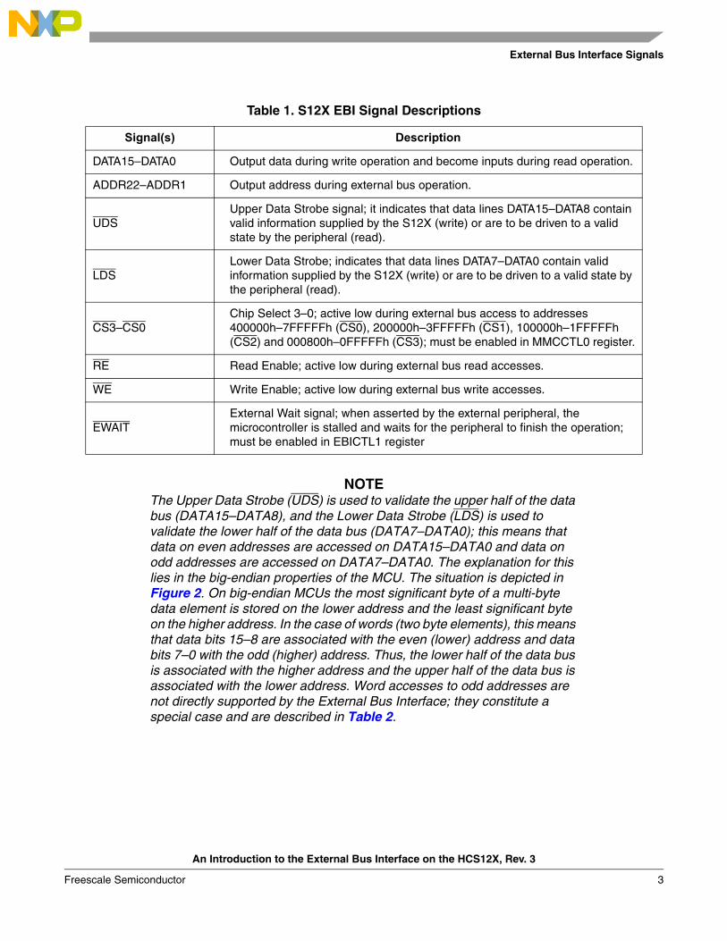
External Bus Interface Signals
A block diagram showing signals associated with the External Bus Interface is shown in Figure 1. A brief description of the functionality of the individual signals is given in Table 1.
S12X
DATA 15:0
ADDR 22:1
WE RE,
*Optional Signal
LDS
CS 3:0*
EWAIT*
UDS
Figure 1. Block Diagram Showing S12X EBI Signals
Signals shown with an asterisk are optional. This means that the user can enable or disable the signal as needed by the application. When a signal is disabled, it assumes its alternative function (i.e., general purpose input/output).
NOTENot all signals are available on all parts of the family or on all package options. Consult the appropriate device user guide for details.
An Introduction to the External Bus Interface on the HCS12X, Rev. 3
2 Freescale Semiconductor
External Bus Interface Signals
Table 1. S12X EBI Signal Descriptions
Signal(s) Description
DATA15–DATA0 Output data during write operation and become inputs during read operation.
ADDR22–ADDR1 Output address during external bus operation.
UDSUpper Data Strobe signal; it indicates that data lines DATA15–DATA8 contain valid information supplied by the S12X (write) or are to be driven to a valid state by the peripheral (read).
LDSLower Data Strobe; indicates that data lines DATA7–DATA0 contain valid information supplied by the S12X (write) or are to be driven to a valid state by the peripheral (read).
CS3–CS0Chip Select 3–0; active low during external bus access to addresses 400000h–7FFFFFh (CS0), 200000h–3FFFFFh (CS1), 100000h–1FFFFFh (CS2) and 000800h–0FFFFFh (CS3); must be enabled in MMCCTL0 register.
RE Read Enable; active low during external bus read accesses.
WE Write Enable; active low during external bus write accesses.
EWAITExternal Wait signal; when asserted by the external peripheral, the microcontroller is stalled and waits for the peripheral to finish the operation; must be enabled in EBICTL1 register
NOTEThe Upper Data Strobe (UDS) is used to validate the upper half of the data bus (DATA15–DATA8), and the Lower Data Strobe (LDS) is used to validate the lower half of the data bus (DATA7–DATA0); this means that data on even addresses are accessed on DATA15–DATA0 and data on odd addresses are accessed on DATA7–DATA0. The explanation for this lies in the big-endian properties of the MCU. The situation is depicted in Figure 2. On big-endian MCUs the most significant byte of a multi-byte data element is stored on the lower address and the least significant byte on the higher address. In the case of words (two byte elements), this means that data bits 15–8 are associated with the even (lower) address and data bits 7–0 with the odd (higher) address. Thus, the lower half of the data bus is associated with the higher address and the upper half of the data bus is associated with the lower address. Word accesses to odd addresses are not directly supported by the External Bus Interface; they constitute a special case and are described in Table 2.
An Introduction to the External Bus Interface on the HCS12X, Rev. 3
Freescale Semiconductor 3

External Bus Interface Signals
even address odd address
bit 15 bit 8 bit 7 bit 0
word access to an even address
even address
bit 15 bit 8
byte access to an even address
odd address
bit 7 bit 0
byte access to an odd address
Figure 2. Association of data bits with addresses
An Introduction to the External Bus Interface on the HCS12X, Rev. 3
4 Freescale Semiconductor

External Bus Operation
External Bus Operation
As already indicated, there are two operations that can be performed on the external bus: read and write. During a write operation, data is transferred from the S12X microcontroller to the peripheral connected to the external bus. During a read operation, the data is transferred in the opposite direction, i.e., from the peripheral into the S12X microcontroller.
Write Operation
During a write operation, the microcontroller performs the following steps.
1. Drives the ADDR, UDS & LDS lines to appropriate levels. Asserts the appropriate CSx signal (if enabled).
2. Drives DATA lines to appropriate levels to represent the data being written.
3. Asserts the WE line.
4. If the EWAIT signal is enabled and was asserted by the peripheral, waits until it is deasserted.
5. Waits the required number of bus cycles (according to the contents of the EBICTL1 register).
6. Deasserts the WE line.
7. Deasserts the CSx line (if asserted and there are no back-to-back writes to be performed; it may stay asserted between back-to-back writes). Stops driving the DATA lines. Deasserts the UDS & LDS lines.*
Read Operation
During a read operation the microcontroller performs the following steps.
1. Drives the ADDR, UDS & LDS lines to appropriate levels. Assert the appropriate CSx signal (if enabled).
2. Asserts the RE line.
3. If the EWAIT signal is enabled and was asserted by the peripheral, waits until it is deasserted.
4. Waits the required number of bus cycles (according to the contents of the EBICTL1 register).
5. Reads data from the DATA lines.
6. Deasserts the RE line. Deasserts the CSx line (if asserted and there are no back-to-back reads to be performed; it may stay asserted between back-to-back reads). Deasserts the UDS & LDS lines.*
* Note: The ADDR lines are always driven by the external bus interface even when there is no external bus access performed. The state of the ADDR lines between accesses (i.e. when UDS, LDS, RE & WE are all high) is undefined. The ASIZ field in the EBICTL0 register can be used to switch the ADDR lines to GPIO functionality in software when a specific behavior is required between external accesses. See page 8 for details.
An Introduction to the External Bus Interface on the HCS12X, Rev. 3
Freescale Semiconductor 5

External Bus Operation
Activity of Bus Signals During Different Types of Operations
The activity of RE, WE, LDS, UDS and Data signals of the External Bus Interface during odd/even and byte/word wide accesses is detailed in Table 2.
Table 2. S12X EBI Signals Activity
Operation RE WE DATA15–8 DATA7–0 UDS LDS
Byte write to even address Inactive Active Data byte Not driven Active Inactive
Byte read from even address Active Inactive Data byteIgnored by MCU
Active Inactive
Byte write to odd address Inactive Active Not driven Data byte Inactive Active
Byte read from odd address Active InactiveIgnored by
MCUData byte Inactive Active
Word write to even address Inactive Active Upper byteLower byte
Active Active
Word read from even address Active Inactive Upper byteLower byte
Active Active
Word write to odd address is split into two consecutive operations
1. The on-chip RAM is capable of word-wide accesses to odd addresses in a single cycle. However on the external bus this type of access is split into two consecutive byte-wide operations. The core is halted during the inserted cycles required for performing the extra access.
(1)
Inactive Active Not drivenUpper byte
Inactive Active
Inactive Active Lower byte Not driven Active Inactive
Word read from odd address is split into two consecutive operations(1)
Active InactiveIgnored by
MCUUpper byte
Inactive Active
Active Inactive Lower byteIgnored by MCU
Active Inactive
Bus Stretch Cycles
When accessing on-chip peripherals and memories, the device performs both 8-bit and 16-bit core accesses in one bus clock cycle. However, when the core accesses locations on the external bus in expanded mode, the accesses are “stretched” and take more than one bus clock cycle to complete. The minimum amount of stretching is one additional bus clock cycle. The number of stretch cycles, and thus also the total number of cycles required for external access, can be influenced by the user, by setting the EXSTRx bits in the EBICTL1 register. This allows the user to adjust the timing of the bus signals based
NOTES:NOTES:
An Introduction to the External Bus Interface on the HCS12X, Rev. 3
6 Freescale Semiconductor

External Bus Operation
on the timing requirements of the devices connected to the external bus. Details of the number of cycles in different configurations are given in Table 3.
Table 3. Number of Stretch Cycles in Different Configurations
EXSTR2 (EBICTL1)
EXSTR1 (EBICTL1)
EXSTR0 (EBICTL1)
EWAITE (EBICTL1)
StretchCycles
Total Cycles
0 0 0 0 1 2
0 0 1 0 2 3
0 1 0 0 3 4
0 1 1 0 4 5
1 0 0 0 5 6
1 0 1 0 6 7
1 1 0 0 7 8
1 1 1 0 8 9
0 0 0 1
1. If the EWAIT feature is enabled, the table shows the minimum number of cycles. Additional stretch cycles will be added if the EWAIT signal is asserted.
2 (1) 3 (1)
0 0 1 1 2 (1) 3 (1)
0 1 0 1 3 (1) 4 (1)
0 1 1 1 4 (1) 5 (1)
1 0 0 1 5 (1) 6 (1)
1 0 1 1 6 (1) 7 (1)
1 1 0 1 7 (1) 8 (1)
1 1 1 1 8 (1) 9 (1)
External WAIT
The External Bus Interface offers a new feature, which allows the external peripherals to stretch accesses to the external bus by asserting the EWAIT signal. To use this feature, the EWAITE bit in the EBICTL1 register must be set by the application. The peripheral can assert the EWAIT signal for as long as necessary to complete the access. However, the core will be stalled in such cases and will not be able to perform any instructions, nor will it be able to respond to any interrupts. In cases where the peripheral asserts the EWAIT signal, the access takes the number of cycles specified by Table 3 plus the time that the EWAIT signal is active. Note that the XGATE co-processor is not stalled when the EWAIT signal is asserted and continues to run.
NOTES:NOTES:
An Introduction to the External Bus Interface on the HCS12X, Rev. 3
Freescale Semiconductor 7

I/O Configuration Options
I/O Configuration Options
Configuring the number of stretch cycles and enabling/disabling the EWAIT signal functionality in EBICTL1 register has been described above. The other options of the external bus interface are related to the required width of the address and data buses.
Size of the Address Bus
The user can freely select the required width of the address bus for the particular application. By limiting the number of address lines (that is, limiting the size of the distinct address locations addressable by the external bus) some of the address lines are freed and can be used as general purpose I/O. The selection is performed by assigning an appropriate value to the ASIZ[4:0] bits in the EBICTL0 register. The lower the value assigned to ASIZ, the lower the number of address lines used by the external bus interface. In the extreme case, where ASIZ bits are assigned a value of 0, none of the address lines are used by the external bus interface and all of them can be used as general purpose I/O pins. The functions of the remaining pins of the external bus interface remain unaffected.
Size of the Data Bus
The external bus interface supports 16 data lines by default. However, only one half of the data lines are required when interfacing to an 8-bit peripheral. In this case, the HDBE bit in the EBICTL0 register can be used to switch off the high byte of the bus interface (lines DATA[15:8]). This enables their use as additional general purpose I/O pins and makes termination of the unused data lines unnecessary, thus reducing the overall cost of the design. The UDS and LDS signals become unnecessary with only one half of the data lines being used for external bus accesses, and these are freed to be used as general purpose I/O when the HDBE bit is cleared.
Threshold Levels
The ITHRS bit in the EBICTL0 register can be used to reduce the input threshold of the external bus interface input signals. This allows the user to connect a 3.3 V peripheral to the external bus when the device is running from a 5 V supply. However, the output lines of the external bus interface will still produce 5 V signals, and care must be taken to ensure that the external 3.3 V peripheral is able to accept 5V input signals.
Limitations and Interfacing Options
Limitations Imposed by Peripherals
The design of the External Bus Interface allows reads as well as writes to individual bytes in the external address space. An example application, which utilizes this feature, can be seen in Figure 3.
An Introduction to the External Bus Interface on the HCS12X, Rev. 3
8 Freescale Semiconductor

Bus Access Timing Diagrams — Examples of Operation
S12X DATA 15:0
ADDR 17:1
WE
LDS
CSn
RE
UDS
WE
UB
CE
OE
LB
GS72116128k x 16
RAM
Figure 3. Using the External Bus to Provide Additional 256K Bytes of RAM
However, not all 16-bit peripheral devices have the capability of accessing individual bytes in their address space. Read operations typically do not present a problem, because, in this event, one half of the bus is simply ignored by the MCU. However, during the write operation, the device may require full 16-bit data, while the MCU may drive only the upper or the lower half of the bus (depending on whether the byte write operation is performed on an odd or even address). This situation leads to unavoidable data corruption inside the peripheral. The simple workaround to resolve this problem is to avoid byte writes if the external peripheral does not have the capability of addressing individual bytes in its address space.
Interfacing to 8-bit Peripherals
The External Bus Interface is primarily designed to interface the MCU to 16-bit peripherals. However, with certain limitations, it can also be used to interface to an 8-bit peripheral (for example, an LCD driver). In this case, the HDBE bit in EBICTL0 register is cleared, only the lower half of the data bus is used, and the LDS and UDS signals are not used by the external bus interface. Registers of the peripheral are then visible on odd addresses only. The fact that the peripheral’s registers are visible on every other address in the memory space presents a problem only if the peripheral contains some sort of linear buffer. Such a buffer would ideally be addressed by the application as a linear array of bytes. In this case two simple workarounds exist:
• Make the array twice as big, and address only every other location in the array.
• Create the array as an array of words, rather than bytes, and ignore the upper byte of every word in the array.
Both workarounds lead to a slight software overhead in the application, but this is relatively minor and can usually be tolerated.
Bus Access Timing Diagrams — Examples of Operation
The diagrams on the following pages are based on real-world measurements; however, they are included for illustration purposes only. The user should always refer to the device specification for exact timing values.
An Introduction to the External Bus Interface on the HCS12X, Rev. 3
Freescale Semiconductor 9

Bus Access Timing Diagrams — Examples of Operation
Figu
re 4
sho
ws
the
rela
tions
hip
betw
een
diffe
rent
ext
erna
l bus
sig
nals
at 4
0 M
Hz
bus
cloc
k op
erat
ion
with
one
str
etch
clo
ck c
ycle
se
lect
ed in
the
EB
ICT
L1 r
egis
ter
and
the
EW
AIT
feat
ure
disa
bled
. The
follo
win
g ex
tern
al b
us a
cces
ses
can
be s
een
in th
e di
agra
m:
1.W
ord
writ
e of
val
ue F
F7E
at a
ddre
ss 0
x3F
FF
FF
2.W
ord
writ
e of
val
ue F
FF
F a
t add
ress
0x3
FF
F7E
3.W
ord
read
from
add
ress
0x3
FF
FF
F
4.W
ord
read
from
add
ress
0x3
FF
F7E
40M
Hz
cloc
k, 1
str
etch
cyc
le
010
020
030
040
050
060
070
080
090
010
00tim
e [n
s]
CS0
CS1
A1
D8
LDS
UD
S
ECLK
RE
WE
12
34
Fig
ure
4. T
imin
g o
f E
xter
nal
Bu
s A
cces
ses
wit
h O
ne
Str
etch
Cyc
le
An Introduction to the External Bus Interface on the HCS12X, Rev. 3
10 Freescale Semiconductor

Bus Access Timing Diagrams — Examples of Operation
Figu
re 5
sho
ws
the
rela
tions
hip
betw
een
diffe
rent
ext
erna
l bus
sig
nals
at 4
0 M
Hz
bus
cloc
k op
erat
ion
with
thre
e st
retc
h cl
ock
cycl
es
sele
cted
in th
e E
BIC
TL1
reg
iste
r an
d th
e E
WA
IT fe
atur
e di
sabl
ed. T
he fo
llow
ing
exte
rnal
bus
acc
esse
s ca
n be
see
n in
the
diag
ram
:
1.W
ord
writ
e of
val
ue F
F7E
at a
ddre
ss 0
x3F
FF
FF
2.W
ord
writ
e of
val
ue F
FF
F a
t add
ress
0x3
FF
F7E
3.W
ord
read
from
add
ress
0x3
FF
FF
F
4.W
ord
read
from
add
ress
0x3
FF
F7E
40M
Hz
cloc
k, 3
str
etch
cyc
les
010
020
030
040
050
060
070
080
090
010
00tim
e [n
s]
CS0
CS1
A1
D8
LDS
UD
S
ECLK
RE
WE
12
34
Fig
ure
5. T
imin
g o
f E
xter
nal
Bu
s A
cces
ses
wit
h T
hre
e S
tret
ch C
ycle
s
An Introduction to the External Bus Interface on the HCS12X, Rev. 3
Freescale Semiconductor 11

Bus Access Timing Diagrams — Examples of Operation
Figu
re 6
sho
ws
the
rela
tions
hip
betw
een
diffe
rent
ext
erna
l bus
sig
nals
at 4
0 M
Hz
bus
cloc
k op
erat
ion
with
two
stre
tch
cloc
k cy
cles
se
lect
ed in
the
EB
ICT
L1 r
egis
ter
and
the
EW
AIT
feat
ure
enab
led.
The
EW
AIT
sig
nal p
rolo
ngs
the
dura
tion
of th
e ac
cess
whe
re it
is
activ
e by
four
furt
her
stre
tch
cycl
es a
nd is
trig
gere
d by
CS
1. A
s th
e di
ffere
nt a
cces
ses
depi
cted
in F
igu
re 6
act
ivat
e bo
th C
S0
and
CS
1, th
e di
agra
m s
how
s ac
cess
es b
oth
with
and
with
out t
he E
WA
IT s
igna
l act
ive.
40M
Hz
cloc
k, 2
str
etch
cyc
les,
4 E
WA
IT c
ycle
s
010
020
030
040
050
060
070
080
090
010
00tim
e [n
s]
CS0
CS1
A1
D8
LDS
UD
S
ECLK
RE
WE
EWA
IT Fig
ure
6. T
imin
g o
f E
xter
nal
Bu
s A
cces
ses
wit
h T
wo
Str
etch
Cyc
les
and
EW
AIT
Fea
ture
En
able
d
An Introduction to the External Bus Interface on the HCS12X, Rev. 3
12 Freescale Semiconductor

References
References
External Bus Interface specification, Freescale Semiconductor, S12XEBIV2
Module Mapping Control specification, Freescale Semiconductor, S12XMMCV2
Data sheet to GS72116, GSI Technology, Rev: 1.04a
NOTEWith the exception of mask set errata documents, if any other Freescale semiconductor document contains information that conflicts with the information in the device data sheet, the data sheet should be considered to have the most current and correct data.
An Introduction to the External Bus Interface on the HCS12X, Rev. 3
Freescale Semiconductor 13

AN2708Rev. 3, 11/2005
How to Reach Us:
Home Page:www.freescale.com
E-mail:[email protected]
USA/Europe or Locations Not Listed:Freescale SemiconductorTechnical Information Center, CH3701300 N. Alma School Road Chandler, Arizona 85224 +1-800-521-6274 or [email protected]
Europe, Middle East, and Africa:Freescale Halbleiter Deutschland GmbHTechnical Information CenterSchatzbogen 781829 Muenchen, Germany+44 1296 380 456 (English)+46 8 52200080 (English)+49 89 92103 559 (German)+33 1 69 35 48 48 (French)[email protected]
Japan:Freescale Semiconductor Japan Ltd. Headquarters ARCO Tower 15F 1-8-1, Shimo-Meguro, Meguro-ku, Tokyo 153-0064 Japan 0120 191014 or +81 3 5437 [email protected]
Asia/Pacific:Freescale Semiconductor Hong Kong Ltd.Technical Information Center 2 Dai King Street Tai Po Industrial Estate Tai Po, N.T., Hong Kong +800 2666 [email protected]
For Literature Requests Only:Freescale Semiconductor Literature Distribution CenterP.O. Box 5405Denver, Colorado 802171-800-441-2447 or 303-675-2140Fax: [email protected]
Information in this document is provided solely to enable system and software implementers to use Freescale Semiconductor products. There are no express or implied copyright licenses granted hereunder to design or fabricate any integrated circuits or integrated circuits based on the information in this document.
Freescale Semiconductor reserves the right to make changes without further notice to any products herein. Freescale Semiconductor makes no warranty, representation or guarantee regarding the suitability of its products for any particular purpose, nor does Freescale Semiconductor assume any liability arising out of the application or use of any product or circuit, and specifically disclaims any and all liability, including without limitation consequential or incidental damages. “Typical” parameters which may be provided in Freescale Semiconductor data sheets and/or specifications can and do vary in different applications and actual performance may vary over time. All operating parameters, including “Typicals” must be validated for each customer application by customer’s technical experts. Freescale Semiconductor does not convey any license under its patent rights nor the rights of others. Freescale Semiconductor products are not designed, intended, or authorized for use as components in systems intended for surgical implant into the body, or other applications intended to support or sustain life, or for any other application in which the failure of the Freescale Semiconductor product could create a situation where personal injury or death may occur. Should Buyer purchase or use Freescale Semiconductor products for any such unintended or unauthorized application, Buyer shall indemnify and hold Freescale Semiconductor and its officers, employees, subsidiaries, affiliates, and distributors harmless against all claims, costs, damages, and expenses, and reasonable attorney fees arising out of, directly or indirectly, any claim of personal injury or death associated with such unintended or unauthorized use, even if such claim alleges that Freescale Semiconductor was negligent regarding the design or manufacture of the part.
Freescale™ and the Freescale logo are trademarks of Freescale Semiconductor, Inc. All other product or service names are the property of their respective owners. © Freescale Semiconductor, Inc. 2005.