an overview of lpddr3 commands, operations, and functions. · an overview of lpddr3 commands,...
TRANSCRIPT

Migrating to LPDDR3:Migrating to LPDDR3:
An overview of LPDDR3 An overview of LPDDR3 commands, operations, and
functions.
LPDDR3 Symposium 2012

ContentsContents• LPDDR2 to LPDDR3 migration
• LPDDR3 Commands: highlights
• LPDDR3 Operations: highlights
• LPDDR3 AC Timing and Signaling

LPDDR3 ObjectiveLPDDR3 Objective
• Increase bandwidth 50% LPDDR2-1066
– From 8.5 GB/s1 to 12.8 GB/sec1
• Fast time-to-market
– Re-use existing LPDDR2 infrastructure
• No change or limited changes to interface, command protocol,
state machine, etc.
• Only changes which enable the higher speed operation should • Only changes which enable the higher speed operation should
be considered.
• SOC vendors and DRAM vendors should re-use as much as
possible from LPDDR2 in order to meet very aggressive time-
to-market.
1. 2-channels

LPDDR3: Key Features LPDDR3: Key Features ComparisonComparison
Feature LPDDR2-S4 LPDDR3
Interface/Bond Pads LPDDR2 Same w/additional ODT pin
Command Protocol LPDDR2 Same
Array Pre-Fetch 4n 8n
Speed Bins 533,400,333,266,200 800,667
Read/Write Latencies 8/4,6/3,5/2,4/2,3/1 12/6,10/6 or optional WL=9Read/Write Latencies 8/4,6/3,5/2,4/2,3/1 12/6,10/6 or optional WL=9
Memory Densities 64Mb – 8Gb 4Gb/6Gb/8Gb (16/32Gb TBD)
Burst Lengths 4,8,16 8 only!
Burst Sequence Sequential,Interleaved Sequential only!
Drive Strength 34,40,48,60,80,120 34,40,48 + asym options
ODT Not supported Added!
Low Power Features (PASR,
TCSR, DPD, etc.)
Supported Supported
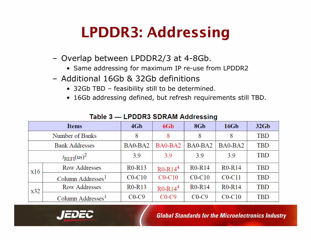
LPDDR3: AddressingLPDDR3: Addressing
– Overlap between LPDDR2/3 at 4-8Gb.• Same addressing for maximum IP re-use from LPDDR2
– Additional 16Gb & 32Gb definitions• 32Gb TBD – feasibility still to be determined.
• 16Gb addressing defined, but refresh requirements still TBD.

LPDDR3: PerformanceLPDDR3: Performance
18
14
Peak Throughput for Mobile Platforms
(GB/s)
WideIO
LPDDR4
WideIO-2
20132011 2015201420122010
14
10
6
2
LPDDR2
LPDDR3
WideIO
2X
4X

LPDDR3: PerformanceLPDDR3: Performance
• 1333/1600 speed bins
– 8n array pre-fetch to support higher tCK
– Min Burst Length 8 supported
– RL/WL/nWR support for each new speed bin• Note WL “set B” support
• Additional RL/WL settings allow for frequency scaling to intermediate speeds with optimized latency settings. Use next intermediate speeds with optimized latency settings. Use next higher speed bin timing specs.
• Future support for higher speeds (266MHz DRAM core)
– LPDDR3e speed extensions under discussion, to support 1866/2133 Mbps (target).

LPDDR3: PowerLPDDR3: Power
• LPDDR2 -> LPDDR3: no change in VDD
• Larger pre-fetch, higher R/W power
• Faster tCK: higher IO power
Low-Power DRAM?
– Power efficiency (pJ/bit) improvement with higher performance – performance increase out-gains power increase…
• 2-ch LPDDR2 delivers 8.3GB/sec at 533MHz, approx 11.9pJ/bit
• 2-ch LPDDR3 delivers 12.8GB/sec at 800MHz, approx 9.2pJ/bit
– Higher performance also allows for faster data transfer of fixed quantity resulting in longer idle time for additional power savings.

LPDDR3: Low Power FeaturesLPDDR3: Low Power Features
• TCSR – same feature as LPDDR2
• PASR – same as LPDDR2 (identical bank & segment masking as S4)
• DPD – supported
• Power-down mode
• Self-refresh mode• Self-refresh mode
• New requirements:
– tCPDED required for PD/SREF/DPD entry
– tMRRI required upon PD exit• Ensures output buffers do not have worst-case scenario after
power-down exit.
Controller backward compatibility to new specs ensured.

LPDDR3: Low Power Mode LPDDR3: Low Power Mode ChangesChanges
• tCPDED
• tMRRI

LPDDR3: Power ManagementLPDDR3: Power Management
• Higher clock speed means higher power, potential thermal concern (esp. PoP).
• Power management features and methods may be employed
– Expect that LPDDR3 may operate in elevated temperature range (+85’C to +105’C).
– MR4 die temp sensor polling enables operation in elevated temp region with refresh de-rating.temp region with refresh de-rating.
– Per-bank refresh enables user to run in extended temp range without performance degradation.
• 17% performance hit when running all-bank refresh at 4x tREFI
elevated temperature refresh requirement.
• Concurrent bank R/W operations with per-bank refresh allows data bus to remain active. (Watch command bus activity though!)

LPDDR3: Power Management LPDDR3: Power Management (continued)(continued)
• Clock frequency scaling
– Utilize alternate RL/WL settings for optimization at a given scaled frequency.
– Optional RL3 setting (see MR0) for <166MHz enables efficient low-frequency operation.
• High speed operation allows for shorter time to transfer a fixed amount of data – utilize power-down between a fixed amount of data – utilize power-down between data transfer for average power reduction.
• Termination will consume power. Optimize ODT and OBT based on SI analysis
– Multi-rank power control must consider ODT pin connections. Rank0 cannot provide termination for Rank1 if in SREF mode.

ContentsContents• LPDDR2 to LPDDR3 migration
• LPDDR3 Commands: highlights
• LPDDR3 Operations: highlights
• LPDDR3 AC Timing and Signaling

LPDDR3: Command TTLPDDR3: Command TT
• With need to support only BL8, no longer support truncated bursts.
• No BST command
• WIW/RIR forbidden

ContentsContents• LPDDR2 to LPDDR3 migration
• LPDDR3 Commands: highlights
• LPDDR3 Operations: highlights
• LPDDR3 AC Timing and Signaling

LPDDR3 Operations: LPDDR3 Operations: InitializationInitialization
• Power Ramp / Initialization Updates
– Changes to enable boot at-speed prior to CA Training (when required).
• Boot at-speed may not be possible if CA bus requires training.
• Insertion of CA training period.• Insertion of CA training period.
• Boot at reduced tCKb still supported.

LPDDR3 Operations: LPDDR3 Operations: InitializationInitialization
CA training should be performed prior to ZQ
Cal; not required if low-speed boot
MRR not used when booting at-speed (DQ calibration, CA training not yet performed)
LPDDR3 Operations: MR0LPDDR3 Operations: MR0
• MR0
– support for WL setB• Similar to additive latency concept in DDR3/DDR4.
• Optional settings with alternate RL/WL ratios for scheduling optimization in different controllers.
– RL3 support option• Low speed operation • Low speed operation

LPDDR3 Operations: MR1LPDDR3 Operations: MR1
• MR1 nWR/BL– Sequential burst support only – subset of LPDDR2 read burst
sequence options.
– nWR support expanded using additional nWRE bit from MR2[4] to allow higher speed operation and support asynchronous tWR timing requirement.

LPDDR3 Operations: MR2LPDDR3 Operations: MR2
• MR2
– Write Lev
– WL set B
– RL/WL• Support for various clock
settings, but not all speed bins defined in AC timing.
• Use of intermediate RL/WL • Use of intermediate RL/WL settings require next higher speed bin timing requirements.
• RL3 support is optional.

LPDDR3: Operations LPDDR3: Operations –– MR3MR3• Asymmetric drive strength settings for data-eye
optimization.
• Asymmetric rise/fall slew rates will cut into data-eye width.
• Margin can be regained using independent control of output drive and resulting slew rates.
• May improve aperture width, common mode power noise, DQS jitter.DQS jitter.

LPDDR3 Operations: MR4LPDDR3 Operations: MR4
• MR4 temp sensor output additional output setting

LPDDR3 Operations: WRITELPDDR3 Operations: WRITE
• Write Preamble changed from low-only to toggle (DDR3-like)
– With DQ termination DQS_t/DQS_c are pulled high prior to a data input operation, making it difficult to detect a DQS transition.
– Toggle preamble allows better detection of DQS crossover.crossover.

LPDDR3 Operations: READLPDDR3 Operations: READ
• LPDDR3 Data Valid Window (DVW) definition has changed from LPDDR2 definition
– Alignment with DDR3 definition
– DVW = tQH – tDQSQ• For LPDDR2: = (tQSH/tQSL)min – tQHSmax - tDQSQ
tQSHmin/tQSLmin – tDQSQmax - tQHSmax
Duty cycle distortion already accounted for in tQSH/tQSL;
DVW Calculation
t = 1250ps
tQSLtQSH
tCKavg = 1250ps
tCH(abs)min = .43 * tCKavg = 537.5ps
tQSHmin = tCH(abs)min – 0.05 * tCKavg = 475ps
tDQSQ = 135ps
DVW = 340ps
UI = .5 * tCKavg = 625ps
%UI = 54.4%

ContentsContents• LPDDR2 to LPDDR3 migration
• LPDDR3 Commands: highlights
• LPDDR3 Operations: highlights
• LPDDR3 AC Timing and Signaling

LPDDR3: AC TimingLPDDR3: AC Timing
• Key spec changes
– 1600/1333 speed bins
• tCK = 1.25ns/1.5ns
• Other tCK require use of next highest speed binsbins
– Input setup/hold
• 150ps/175ps
– Potential for LPDDR3E?
• 1866/2133 speed bins
• Setup/hold timing budget very challenging.
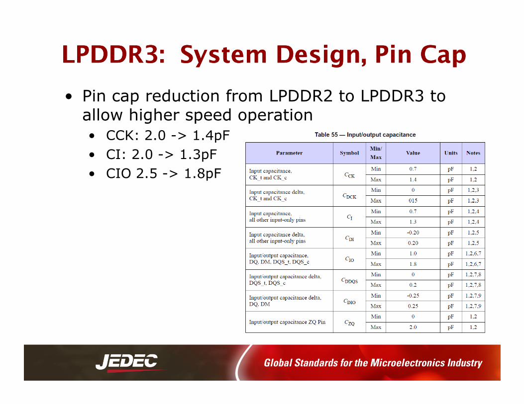
LPDDR3: System Design, Pin CapLPDDR3: System Design, Pin Cap
• Pin cap reduction from LPDDR2 to LPDDR3 to allow higher speed operation
• CCK: 2.0 -> 1.4pF
• CI: 2.0 -> 1.3pF
• CIO 2.5 -> 1.8pF

LPDDR3: System Design LPDDR3: System Design ConsiderationsConsiderations
• Signal integrity is significantly affected by these parameters:– CIO (capacitance)
– Driver slew rate
– Package design
– Power delivery (key in PoP implementation)
• Great care must be taken to design a system that has • Great care must be taken to design a system that has good signal integrity at 1600 MT/s with this PHY
• It is highly recommended to work with memory vendors to model your system using extracted driver and package parameters
• Additional features can be employed to improve signal margin
– DQ On Die Termination (ODT)
– Asym drive strength