an11740 pn5180 antenna design guide - nxp ... pn5180 antenna design guide rev. 1.0 — 19 november...
TRANSCRIPT

AN11740 PN5180 Antenna design guide Rev. 1.1 — 19 June 2018 345311
Application note COMPANY PUBLIC
Document information Info Content Keywords PN5180, Antenna design, Antenna tuning
Abstract This document describes the “standard” antenna design and tuning related to the PN5180.

NXP Semiconductors AN11740 PN5180 Antenna design
AN11740 All information provided in this document is subject to legal disclaimers. © NXP B.V. 2018. All rights reserved.
Application note COMPANY PUBLIC
Rev. 1.1 — 19 June 2018 345311
2 of 62
Contact information For more information, please visit: http://www.nxp.com
Revision history Rev Date Description 1.1 20180619 Editorial updates
1.0 20151119 First release

NXP Semiconductors AN11740 PN5180 Antenna design
AN11740 All information provided in this document is subject to legal disclaimers. © NXP B.V. 2018. All rights reserved.
Application note COMPANY PUBLIC
Rev. 1.1 — 19 June 2018 345311
3 of 62
1. Introduction The antenna design for the PN5180 is not much different than the antenna design for most of the other NXP reader ICs in general. However, some PN5180 specific details need to be considered to get an optimum performance.
This document describes the generic NFC and RFID antenna design rules in section 3 as simple as possible, considering the different requirements due to ISO/IEC 14443, NFC or EMVCo as introduced in section 2 and 3.
The section 4 describes the antenna design for the PN5180 in detail for mainly the standard “asymmetrical” antenna tuning. The “symmetrical” tuning is shown, but requires the “Dynamic Power Control” (DPC). Dedicated ANs describing the DPC related “symmetrical” tuning in detail together with the calibration and use of the DPC (see [14] and [15]).
In the Annex in section 5 some basics about the antenna impedance measurement and the related tools can be found.
1.1 Dynamic Power Control The Dynamic Power Control (DPC) feature of the PN5180 allows an improved antenna design (called “DPC antenna design”) with improved transfer function. The DPC antenna design and the specifics of the DPC are described in detail in [14] and [15].
2. NFC Reader Antenna design For the NFC operation three different communication modes are specified in [4]:
1. In the card emulation mode (CM) the NFC device can be used in (existing) NFC reader infrastructure. In the CM the NFC device behaves in principle like a PICC, as defined in [2]. This mode is optional.
2. In the card reader mode (RM) the NFC device can be used with (existing) NFC cards. In the RM the NFC device behaves in principle like a PCD, as defined in [2]. This mode is mandatory.
3. In the peer to peer mode (P2P) the NFC device can communicate to other NFC devices, either being the initiator, starting the communication, or being the target, answering the communication.
The Fig 1 shows the NFC device in the center, offering all three NFC communication modes. For the communication between two NFC devices the two different P2P modes are available:
1. Active P2P: Both NFC devices, the initiator as well as the target, are required to generate their own magnetic field, when sending data. This mode is optional.
2. Passive P2P: The initiator always generates the magnetic field, while the target uses the load modulation principle to send its data. This mode is mandatory.
In this document only the analog topics are discussed, which are relevant for the antenna design. Neither the digital protocol nor the advantages/disadvantages for different use cases are content of this document.

NXP Semiconductors AN11740 PN5180 Antenna design
AN11740 All information provided in this document is subject to legal disclaimers. © NXP B.V. 2018. All rights reserved.
Application note COMPANY PUBLIC
Rev. 1.1 — 19 June 2018 345311
4 of 62
For the optimization of the performance it might makes sense to restrict the functionality to only one or two of the communication modes.
(1) ISO/IEC 14443 PICC and PCD here just indicate the similarity of the communication but do not automatically mean interoperability.
(2) “Extended ISO/IEC14443 PCD/PICC” simply refers to the antenna design parameters and does not include the protocol.
Fig 1. NFC communication modes
2.1 ISO/IEC 14443 specifics The ISO/IEC 14443 (called “ISO” in the following, details see [2]) specifies the contactless interface as widely being used with contactless smartcards.
The ISO/IEC 14443 defines the communication between a reader (“proximity coupling device” = PCD) and a contactless smartcard (“proximity chip card” = PICC). In four parts it describes the physical characteristics (i.e. the size of the PICC antennas), the analog parameters like e.g. modulation and coding schemes, the card activation sequences (“Anticollision”) and the digital protocol. The ISO/IEC 10373-6 (see [3]) describes the test setup as well as all the related tests for cards and the reader.
The ISO/IEC 14443 reader antenna consists of an antenna coil, which is matched to the reader IC. This antenna coil, as shown in Fig 2,
1. generates the magnetic field to provide the power to operate a card (PICC),
2. transmits the data from the reader (PCD) to the card (PICC), and
3. receives the data from the card (PICC) to the reader (PCD).

NXP Semiconductors AN11740 PN5180 Antenna design
AN11740 All information provided in this document is subject to legal disclaimers. © NXP B.V. 2018. All rights reserved.
Application note COMPANY PUBLIC
Rev. 1.1 — 19 June 2018 345311
5 of 62
(1) k = coupling coefficient (2) Φ = magnetic flux
Fig 2. Magnetic coupling between reader (PCD) and card (PICC)
According to the ISO/IEC 14443 the PICC antenna coils can be categorized into the classes 1 …6, as shown in Fig 3.
The PCD antenna is not defined as such, but the PCD must support the classes 1, 2, and 3. The support of the classes 4, 5, and 6 is optional.

NXP Semiconductors AN11740 PN5180 Antenna design
AN11740 All information provided in this document is subject to legal disclaimers. © NXP B.V. 2018. All rights reserved.
Application note COMPANY PUBLIC
Rev. 1.1 — 19 June 2018 345311
6 of 62
(1) A PCD must always support the classes 1, 2, and 3. The Classes 4, 5 and 6 are optional.
Fig 3. PICC Classes according to the ISO/IEC 14443
The PCD antenna coil sizes are not specified. So, for ISO/IEC 14443 compliant readers all different sizes of antenna coils from a few 10 mm2 up to 20cm diameter can be found in various shapes.
The ISO/IEC 14443 does not specify an operating volume. The reader manufacturer needs to guarantee that within the operating volume - that he himself defines - all related ISO/IEC 10373-6 tests can be passed.
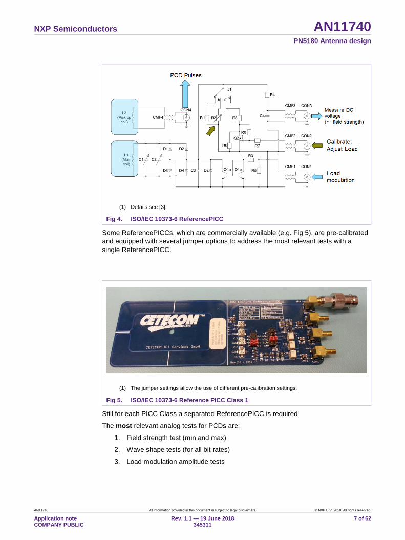
The compliance tests require calibrated ReferencePICCs, as defined in ISO/IEC10373-6. The schematic of such ReferencePICC is shown in Fig 4. For each PICC Class there is one Reference PICC, which needs to be calibrated according to the required measurement. Practically it makes sense to use one calibrated ReferencePICC for each measurement case.
NXP Semiconductors AN11740 PN5180 Antenna design
AN11740 All information provided in this document is subject to legal disclaimers. © NXP B.V. 2018. All rights reserved.
Application note COMPANY PUBLIC
Rev. 1.1 — 19 June 2018 345311
7 of 62
(1) Details see [3].
Fig 4. ISO/IEC 10373-6 ReferencePICC
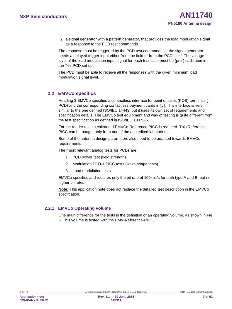
Some ReferencePICCs, which are commercially available (e.g. Fig 5), are pre-calibrated and equipped with several jumper options to address the most relevant tests with a single ReferencePICC.
(1) The jumper settings allow the use of different pre-calibration settings.
Fig 5. ISO/IEC 10373-6 Reference PICC Class 1
Still for each PICC Class a separated ReferencePICC is required.
The most relevant analog tests for PCDs are:
1. Field strength test (min and max)
2. Wave shape tests (for all bit rates)
3. Load modulation amplitude tests

NXP Semiconductors AN11740 PN5180 Antenna design
AN11740 All information provided in this document is subject to legal disclaimers. © NXP B.V. 2018. All rights reserved.
Application note COMPANY PUBLIC
Rev. 1.1 — 19 June 2018 345311
8 of 62
Note: This application note does not replace the detailed test description in the ISO/IEC 10373-6.
There is no common certification process for ISO/IEC14443 compliance in place, even though many national bodies use the ISO/IEC 14443 to operate the electronic passports and electronic ID cards. For these programs some nations have established a certification process to guarantee interoperability. An example is given in [5].
2.1.1 Field strength tests For the field strength test, it is preferred to have the PCD send a continuous carrier, i.e. it performs no modulation.
The field strength tests simply require the calibrated ReferencePICC and a dc voltage measurement device (volt meter or oscilloscope). The field strength is equivalent to the calibrated (and required) voltage level. The ISO/IEC 10373-6 defines minimum voltage levels, corresponding to the minimum required field strength, and maximum voltage levels, corresponding to the maximum allowed field strength. The measured voltage levels must stay in between these limits.
2.1.2 Wave shape tests The PCD needs to send the related pulse(s): It may send an ISO/IEC 14443 REQA and / or REQB with the required bit rate, as e.g. specified in [5]. Any other command fits the purpose, too.
Note: For the test of higher bit rates it makes sense to implement some specific test commands, which send artificial commands, e.g. REQA and / or REQB, using the coding and modulation of the corresponding higher bit rates. The standard way of activating higher bitrates cannot be applied, since the ReferencePICC for ISO/IEC 14443-2 tests does not allow the protocol layer, which is normally required to switch to higher bit rates.
The wave shape tests require 1. a calibrated ReferencePICC, which is placed at the position of the calibrated field
strength (corresponding to the dc voltage as measured in section 2.1.1), 2. a digital oscilloscope with a measurement bandwidth of 500Msamples or higher, and 3. a tool that filters and transforms the oscilloscope data into the envelope signal
according to the ISO/IEC 10373-6.
The tool normally returns the filtered and transformed envelop as well as the corresponding values of rise and fall times, residual carrier levels and over- and undershoots, which must be kept within the given limits.
2.1.3 Load modulation tests The PCD needs to send a teat command, which allows to check a response from the ReferencePICC.
The load modulation tests require 1. a calibrated ReferencePICC, which is placed at the position of the calibrated field
strength (corresponding to the dc voltage as measured in section 2.1.1),
NXP Semiconductors AN11740 PN5180 Antenna design
AN11740 All information provided in this document is subject to legal disclaimers. © NXP B.V. 2018. All rights reserved.
Application note COMPANY PUBLIC
Rev. 1.1 — 19 June 2018 345311
9 of 62
2. a signal generator with a pattern generator, that provides the load modulation signal as a response to the PCD test commands.
The response must be triggered by the PCD test command, i.e. the signal generator needs a delayed trigger input either from the field or from the PCD itself. The voltage level of the load modulation input signal for each test case must be (pre-) calibrated in the TestPCD set up.
The PCD must be able to receive all the responses with the given minimum load modulation signal level.
2.2 EMVCo specifics Heading 3 EMVCo specifies a contactless interface for point of sales (POS) terminals (= PCD) and the corresponding contactless payment cards in [6]. This interface is very similar to the one defined ISO/IEC 14443, but it uses its own set of requirements and specification details. The EMVCo test equipment and way of testing is quite different from the test specification as defined in ISO/IEC 10373-6.
For the reader tests a calibrated EMVCo Reference PICC is required. This Reference PICC can be bought only from one of the accredited labatories.
Some of the antenna design parameters also need to be adapted towards EMVCo requirements.
The most relevant analog tests for PCDs are:
1. PCD power test (field strength)
2. Modulation PCD-> PICC tests (wave shape tests)
3. Load modulation tests
EMVCo specifies and requires only the bit rate of 106kbit/s for both type A and B, but no higher bit rates.
Note: This application note does not replace the detailed test description in the EMVCo specifcation.
2.2.1 EMVCo Operating volume One main difference for the tests is the definition of an operating volume, as shown in Fig 6. This volume is tested with the EMV-Reference-PICC.

NXP Semiconductors AN11740 PN5180 Antenna design
AN11740 All information provided in this document is subject to legal disclaimers. © NXP B.V. 2018. All rights reserved.
Application note COMPANY PUBLIC
Rev. 1.1 — 19 June 2018 345311
10 of 62
(1) Details see [6].
Fig 6. EMVCo POS operating volume requirement
Within this volume the given parameters need to be fulfilled.
2.2.2 EMVCo field strength For the field strength test, it is preferred to have the PCD send a continuous carrier, i.e. it performs no modulation.
The voltage level which can be measured in all of the given positions needs to be between the minimum and maximum limit, as given in [6].
Due to the operating volume it can become challenging to meet the EMVCo requirements with small antennas.
The Fig 7 shows the required power versus antenna size. The curve is based on a antenna simulation, which uses a few simplifications, so it does not take the loading effect of the EMVCo Reference PICC into account. On the other the simulation was done under ideal environmental conditions, i.e. no metal environment influences the antenna. The simulation results can be taken as reference to estimate the design effort especially for small antennas compared to “normal” antenna sizes.

NXP Semiconductors AN11740 PN5180 Antenna design
AN11740 All information provided in this document is subject to legal disclaimers. © NXP B.V. 2018. All rights reserved.
Application note COMPANY PUBLIC
Rev. 1.1 — 19 June 2018 345311
11 of 62
(1) Side length of a square antenna. (2) These simulation results do neither take any specific environment nor loading effects into account.
Fig 7. EMVCo POS Reader antenna size
2.2.3 EMVCo Wave shapes The PCD needs to send the related pulse(s): It may send an EMVCo REQA and / or REQB.
The wave shape tests require 3. a calibrated EMVCo ReferencePICC, which is placed at each of the given position
(see Fig 6), 4. a digital oscilloscope with a measurement bandwidth of 500Msamples or higher, and 5. a tool that filters and transforms the oscilloscope data into the envelope signal
according to the EMVCo test requirement.
The tool normally returns the filtered and transformed envelop as well as the corresponding values of rise and fall times, residual carrier levels and over- and undershoots, which must be kept within the given limits.
2.2.4 EMVCo Load modulation The PCD needs to send a test command, which allows to check a response from the ReferencePICC. Typically, the EMVCo loop back command sequence is used for this.
Note: Since these tests do not replace the certification tests as required by EMVCo, simple tests commands might be even more useful than the full EMVCo test sequence. Such a simple test command can be easily debugged and typically allows an easier triggering.

NXP Semiconductors AN11740 PN5180 Antenna design
AN11740 All information provided in this document is subject to legal disclaimers. © NXP B.V. 2018. All rights reserved.
Application note COMPANY PUBLIC
Rev. 1.1 — 19 June 2018 345311
12 of 62
The load modulation tests require 6. a calibrated ReferencePICC, which is placed at each of the given position (see Fig
6), 7. a signal generator with a pattern generator, that provides the load modulation signal
as a response to the PCD test commands.
The response must be triggered by the PCD test command, i.e. the signal generator needs a delayed trigger input either from the field or from the PCD itself. The voltage level of the load modulation input signal for each test case must be set according to [6].
The PCD must be able to receive all the responses with the given minimum load modulation signal level.
2.3 The NFC specifics The standard NFC device needs to fulfill the reader mode (PCD), the passive target and the passive initiator. The passive target from an antenna point of view is very similar to the optional card mode (PICC).
2.3.1 NFC Operating volume The NFC Forum specifies an operating volume as shown in Fig 8. All specified parameters are tested at given test points within this volume. This is valid not only for reader mode tests, but all tests.
(1) Details see NFC Analog Technical Specification, [4]
Fig 8. NFC Forum operating volume

NXP Semiconductors AN11740 PN5180 Antenna design
AN11740 All information provided in this document is subject to legal disclaimers. © NXP B.V. 2018. All rights reserved.
Application note COMPANY PUBLIC
Rev. 1.1 — 19 June 2018 345311
13 of 62
3. Generic PCD antenna design rules Some of the antenna and analog design rules are very common for NXP NFC Reader designs, i.e. they do neither specifically depend on the used standard (ISO, NFC or EMVCo) nor depend on the NXP Reader IC but rather on physical or technical basics.
3.1 Optimum Antenna Coil The optimum antenna coil size for a standard PCD can be derived from the Biot-Savart law. The major prerequisites are some simplifications like the assumption that the antenna system is optimized based on the parallel operation of smart cards on top of the PCD antenna. The optimization is derived for the operating distance, i.e. the target is to show the optimum PCD antenna size for a given required operating distance.
The principle and simplified electrical circuit is shown in Fig 9.
(1) Index 1: PCD (2) Index 2: PICC
Fig 9. PCD & PICC Antenna coil system
The index 2 indicates the parameters of the PICC. Here the PICC is taken as given, i.e. the parameters with the index 2 cannot be modified. This is another simplification, but also refers to the reality, where the reader antenna optimization does not allow to change card parameters.
The PCD antenna is taken as a circular antenna to allow a simple calculation. The impact of different form factors is discussed later.
Out of this law the coupling coefficient k between PCD and PICC antenna can be described as following:

NXP Semiconductors AN11740 PN5180 Antenna design
AN11740 All information provided in this document is subject to legal disclaimers. © NXP B.V. 2018. All rights reserved.
Application note COMPANY PUBLIC
Rev. 1.1 — 19 June 2018 345311
14 of 62
A2 = Card antenna coil area, fixed
L02 = Card antenna coil single turn inductance, fixed
L01 = Reader coil single turn inductance
r = Reader Antenna coil radius
x = Operating distance in the center of the Reader antenna
µ0 = relative permeability
The single turn inductance can be described like this:
d = coil wire diameter with d << r
Note: The formula to calculate the inductance of the antenna coil can only be taken as reference. In real life many details influence the result, which are not taken into account in this simple formula. So a measurement of the coil parameters as described below is required anyway.
3.1.1 Number of turns Changing the number of turns does not change the coupling, since the inductance itself has no influence on the coupling. So, in principle antenna coils with a single turn can be used as well as antenna coils with many turns.
The only remaining parameter to optimize the coupling is the antenna radius r (i.e. the antenna size), and will be discussed in section 3.1.2.
However, the number of turns changes the inductance which on one hand changes the matching circuit.
Out of experience it turns out to be optimum to have an inductance around L ≈ 1µH for a proper matching, but a wide range of L ≈ 300nH up to L≈ 4µH still can be matched properly, so typically 1 up to 4 turns in the normal range of antenna sizes are used.
The Fig 10 shows the typical inductance values versus the antenna coil radius for 1, 2, 3 and 4 turns. These values are just examples, since the environment, the track width or wire thickness and some other parameters may influence the inductance.
Furthermore, the typical PCD antenna coil does not use the circular shape, but rather a rectangular form factor. The given calculated values show the wide range that can be used, and shall be used as reference only. The antenna coil inductance must be measured anyway later on to do the antenna matching.
0201
2
2322
2
0)(2 LL
A
xr
rk⋅
⋅+
⋅= µ (1)
[ ] )2ln(2102 7
01 drr
mL ⋅
⋅⋅⋅⋅
≈− ππ
(2)

NXP Semiconductors AN11740 PN5180 Antenna design
AN11740 All information provided in this document is subject to legal disclaimers. © NXP B.V. 2018. All rights reserved.
Application note COMPANY PUBLIC
Rev. 1.1 — 19 June 2018 345311
15 of 62
(1) Green area: target area for standard antenna matching.
Fig 10. Inductance examples versus coil radius
On the other hand, the number of turns defines the relationship of voltage level versus current level. Especially for the load modulation (see Fig 11) it might be helpful to increase the number of turns on the PCD antenna coil.
(1) Index1 = PCD (2) Index 2 = PICC antenna coil
Fig 11. Load modulation

NXP Semiconductors AN11740 PN5180 Antenna design
AN11740 All information provided in this document is subject to legal disclaimers. © NXP B.V. 2018. All rights reserved.
Application note COMPANY PUBLIC
Rev. 1.1 — 19 June 2018 345311
16 of 62
3.1.2 Optimum Antenna Coil size Fig 12 shows the coupling coefficient versus antenna radius for three different operating distances. The scaling of the coupling coefficient does not necessarily show the correct absolute value, since some of the fixed parameters are estimated only for this graph. However, the relative value is important to indicate the optimum antenna size.
(1) Green: at a distance of x = 4 cm (2) Blue: at a distance of x = 6 cm (3) Black: at a distance of x = 8 cm (4) The coupling coefficient scaling in this diagram is relative only. The absolute value might differ.
Fig 12. Coupling coefficient vs PCD antenna radius
The maximum coupling can be achieved, when
r = Reader Antenna coil radius
x = Operating distance in the center of the Reader antenna
The maximum coupling at an operating distance of 4cm can be achieved with an antenna coil of approximately 4cm radius (i.e. 8cm diameter). Increasing the antenna radius from 4cm to 8cm decreases the coupling at 4cm distance (green curve), but increases the coupling at 8cm distance (black curve).
However, the optimum antenna size as such does not guarantee that the coupling is strong enough.
xr = (3)

NXP Semiconductors AN11740 PN5180 Antenna design
AN11740 All information provided in this document is subject to legal disclaimers. © NXP B.V. 2018. All rights reserved.
Application note COMPANY PUBLIC
Rev. 1.1 — 19 June 2018 345311
17 of 62
The maximum coupling coefficient versus the operating distance can be estimated as shown in Fig 13. This maximum coupling is related to the optimum antenna size.
(1) The absolute scale of k might not be correct due to simplifications.
Fig 13. Maximum coupling vs antenna size
Theoretical example:
The Fig 14 shows the field strength versus operating distance of two different antenna sizes. For both antennas the antenna current is tuned to deliver the maximum allowed field strength of 7.5 A/m at the minimum operating distance of 2mm.
The small antenna with 4cm diameter achieves an operating distance of almost 3cm, the large antenna with 10cm diameter achieves an operating distance of almost 7cm.

NXP Semiconductors AN11740 PN5180 Antenna design
AN11740 All information provided in this document is subject to legal disclaimers. © NXP B.V. 2018. All rights reserved.
Application note COMPANY PUBLIC
Rev. 1.1 — 19 June 2018 345311
18 of 62
(1) Minimum required field strength Hmin = 1.5A/m (2) Both antennas scaled to deliver Hmax = 7.5 A/m at maximum
Fig 14. Operating distance x versus antenna size
Note: The large antenna is driven with a current Ilargeantenna ≈ 4x Ismallantenna.
Note: This graph does not include the detuning and loading effect of the reader antenna.
The Fig 15 shows the simulation result of three different square antennas. The magnitude of the field strength is shown versus the distance from the center of the antenna area in either X or Y direction. The curves indicate the zero points, which are areas around the antenna slightly outside the antenna area, where no field can be measured (i.e. where the coupling is zero).
At a zero point no tag device can be operated, even if the required field strength is very low. This needs to be considered, if there is a requirement to read tags within a certain given operating volume, which might touch the zero points, especially if the antenna is too small.

NXP Semiconductors AN11740 PN5180 Antenna design
AN11740 All information provided in this document is subject to legal disclaimers. © NXP B.V. 2018. All rights reserved.
Application note COMPANY PUBLIC
Rev. 1.1 — 19 June 2018 345311
19 of 62
(1) Operating distance = 1cm, X and Y = horizontal distance from antenna center. (2) These simulation results do neither take any specific environment nor loading effects into account
Fig 15. Magnitude of field strength in 1 cm distance
Note: The field strength is not the same for all three antennas, but has been adjusted individually to achieve the maximum allowed field strength for each antenna.
3.2 Layout recommendations The connection between the TX output pins (TX1 and TX2) and the EMC low pass filter has to be as short as possible. The GND connection especially between TVSS and the C0A and C0B (see Fig 18) capacitors must be as short as possible.
The connection between the block capacitors and the VDD pins need to be as short as possible. This holds especially for the TVDD and its block capacitor.
The PN5180 evaluation board and its related description (see [9]) can be taken as a reference.
The Fig 16 and Fig 17 show a part of the top and bottom layer structure around the PN5180 as reference. The GND layer is a complete area of one of the middle layers (not shown).

NXP Semiconductors AN11740 PN5180 Antenna design
AN11740 All information provided in this document is subject to legal disclaimers. © NXP B.V. 2018. All rights reserved.
Application note COMPANY PUBLIC
Rev. 1.1 — 19 June 2018 345311
20 of 62
(1) Part of the top layer (2) Middle Layer = GND area
Fig 16. PN5180 Layout Reference Board Top layer

NXP Semiconductors AN11740 PN5180 Antenna design
AN11740 All information provided in this document is subject to legal disclaimers. © NXP B.V. 2018. All rights reserved.
Application note COMPANY PUBLIC
Rev. 1.1 — 19 June 2018 345311
21 of 62
(1) Part of the bottom layer (2) Middle Layer = GND area
Fig 17. PN5180 Layout Reference Board Bottom layer
4. PN5180 hardware design The PN5180 is optimized to support the NFC, ISO and EMVCo with a minimum of additional components. The PN5180 simply requires the antenna matching circuitry, some block capacitors and the crystal.
However, the calculation and tuning of the matching components need to be done carefully to provide the full performance as well as to meet CE and FCC regulations.
The Fig 18 and Fig 19 show a typical analog circuitry using the PN5180.

NXP Semiconductors AN11740 PN5180 Antenna design
AN11740 All information provided in this document is subject to legal disclaimers. © NXP B.V. 2018. All rights reserved.
Application note COMPANY PUBLIC
Rev. 1.1 — 19 June 2018 345311
22 of 62
(1) Names to be adapted! (2) Tbd: “to be defined”, need to be defined using this document. (3) CXx, CAntx, C0x, C1x and C2x must be NP0.
Fig 18. Typical PN5180 analog circuit
(1) Names to be adapted! (2) Tbd: “to be defined”, need to be defined using this document. (3) CXx, CAntx, C0x, C1x and C2x must be NP0.
Fig 19. Antenna circuit
The antenna typically is a part of the PCB design (see section 3.2). All capacitors are typical ceramic capacitors (e.g. X7R), except the capacitors used in the matching

NXP Semiconductors AN11740 PN5180 Antenna design
AN11740 All information provided in this document is subject to legal disclaimers. © NXP B.V. 2018. All rights reserved.
Application note COMPANY PUBLIC
Rev. 1.1 — 19 June 2018 345311
23 of 62
circuitry and those connected to the crystal. Those capacitors CXx, CAntx, C0x, C1x and C2x must be NP0.
The inductor L0x must be capable of driving the required power: In case the maximum output power is needed, the L0x must be able to drive the 200mA without going into saturation.
Note: Be aware of tolerances! The most critical tolerance in the antenna circuits appears at the antenna coil itself, but even for the matching circuitry tolerances of < ±1% are recommended.
4.1 PN5180 requirements The PN5180 is optimized to support the EMVCo operating volume. Therefore, the Tx output can drive up to ITVDD = 250mA. Based on a power supply voltage VBAT = TVDD = 5V that means a possible total power consumption for the total antenna circuit of up to Ptot > 1W.
The power supply must be designed properly to be able to deliver a clean supply voltage.
Note: Every noise level on top of the supply voltage can disturb the performance of the PN5180. Therefore, sometimes higher values of the block capacitors in the range of up to 10µF might help to improve the performance.
The PN5180 provides an NMOS/NMOS Push-Pull output stage to drive the antenna circuit. The output impedance of each Tx outputs is approximately 1…3 Ohm (with maximum GSN settings), so basically the antenna impedance itself controls the ITVDD, and therefor the field strength.
The Fig 20 shows the driver current ITVDD versus the antenna impedance. The target impedance to get a maximum field strength and power transfer should be close to 20Ω.

NXP Semiconductors AN11740 PN5180 Antenna design
AN11740 All information provided in this document is subject to legal disclaimers. © NXP B.V. 2018. All rights reserved.
Application note COMPANY PUBLIC
Rev. 1.1 — 19 June 2018 345311
24 of 62
(1) Antenna impedance tuned and measured between TX1 and TX2
Fig 20. ITVDD versus antenna impedance
4.2 Antenna for reader mode If the PN5180 is used in pure reader mode only, i.e. the PN5180 is not used in card mode or as passive P2P target, the ANT1 and ANT2 pins do not need to be used.
In such case the CAntx are not used, and the corresponding design is done without considering the PLM (passive load modulation).
In this document the focus is on the asymmetrical antenna tuning. The principle of the tuning and matching of the symmetrical antenna tuning is very similar, using the same tuning steps. However, the detailed specifics related to the symmetrical antenna tuning and especially to the related DTC can be found in [14].
4.2.1 Antenna matching For the proper antenna design the antenna impedance must be measured using an impedance analyzer or VNA (vector network analyzer). Such a VNA can be a high-end tool from Agilent or Rohde & Schwarz (like the R&S ZVL (see Ref. [7]), as normally used in this document), but might be a cheap alternative with less accuracy like e.g. the miniVNA Pro (see [8]). In any case the analyzer needs to be able to measure the impedance in magnitude and phase (vector).
Such VNA can be used to measure the antenna coil as well as the antenna impedance including the matching circuit.
The antenna matching is done with the following steps: 8. Measure the antenna coil 9. Define target impedance and Q-factor
10. Define the EMC filter

NXP Semiconductors AN11740 PN5180 Antenna design
AN11740 All information provided in this document is subject to legal disclaimers. © NXP B.V. 2018. All rights reserved.
Application note COMPANY PUBLIC
Rev. 1.1 — 19 June 2018 345311
25 of 62
11. Calculate the matching components 12. Simulate the matching 13. Assembly and measurement 14. Adaptation of simulation 15. Correction and assembly
The details of those steps are described in with an example, using the PN512 Bueboard antenna together with the PN5180. The blocks and components are used as shown in Fig 21.
(1) This circuit only covers the Tx part.
Fig 21. PN5180 Reader only antenna matching circuit
4.2.1.1 Measure the antenna coil
The antenna coil must be designed as described in section 3 and be measured. The measurement is required to derive the inductance L, the resistance RCoil and the capacitance Cpa as accurate as possible.
The easiest even though not most accurate way is to use the VNA to measure the impedance Z of the antenna coil at 13.56MHz and to calculate L and R out of it:
Typically, the VNA directly can show the L and R, as shown in Fig 22 and Fig 23.
CoilLjRZ ω+= (4)

NXP Semiconductors AN11740 PN5180 Antenna design
AN11740 All information provided in this document is subject to legal disclaimers. © NXP B.V. 2018. All rights reserved.
Application note COMPANY PUBLIC
Rev. 1.1 — 19 June 2018 345311
26 of 62
(1) Measurement with R&S ZVL
Fig 22. Measurement 1 Antenna coil of PN512 Blueboard
(1) Measurement with miniVNA Pro and vna/J
Fig 23. Measurement 2 Antenna coil of PN512 Blueboard
In this example the antenna coil is measured with these values:
L = 1.5 µH

NXP Semiconductors AN11740 PN5180 Antenna design
AN11740 All information provided in this document is subject to legal disclaimers. © NXP B.V. 2018. All rights reserved.
Application note COMPANY PUBLIC
Rev. 1.1 — 19 June 2018 345311
27 of 62
RCoil = 2.8 … 3.4Ω
Cpa = not measured, can be estimated
The inductance can be measured quite accurate, but the resistance is not very accurate due to the relationship between R and jωL. And the capacitance is not measured at all with this simple measurement.
There are several ways to improve the accuracy and even further derive the capacitance, but these simple results are enough to start the tuning procedure. This tuning procedure needs to be done anyway, so there is no real need to spend more effort in measuring the antenna coil parameters more accurate.
4.2.1.2 Define target impedance and Q-factor
The target impedance must be defined. For the maximum power transfer, it should be 18…20Ω (as indicated in section 4.1). In such case the driver current ITVDD gets close to the limit of ITVDDmax = 250mA.
The impedance target might be different for different applications. An impedance target of Rmatch = 50…80Ω might be better in battery powered devices, where the current consumption must be minimum, while at the same time the required maximum operating distance can be lower.
Note: The following examples show the design for a maximum power transfer, e.g. for an EMVCo POS design.
The quality factor Q depends on the overall system requirements and frame conditions. The overall system requires the Q to be in a range, which allows us to meet the timing and pulse shape requirements of the corresponding standard (ISO, NFC or EMV). These requirements are mainly the same, but with some differences:
While ISO allows data rates of up 848 kbit/s, NFC allows the data rates of up to 424 kbit/s. EMV systems are limited to 106 kbit/s. So typically, the Q of EMV reader systems can be higher than the Q of ISO or NFC reader systems.
The Q is an indirect value, since the measurement of the Q in the overall antenna system, which includes the antenna driver as well as the contactless card, is complex – and not required. The wave shape and timing measurements, as required according to the standards, are the relevant measurements, and the corresponding Q value is not of any importance.
Here in a first step the Q is chosen for the passive and linear antenna circuit only. So, it can be seen as start value to calculate the damping resistors RQ.
Good starting values as entry for the calculation of the matching calculation are shown in Table 1.
Table 1. Q-factor Values for the passive linear antenna circuit only Q Condition 20 Start value for the matching calculation for typical NFC Reader design.
25 Start value for the matching calculation for typical NFC Reader design, limited to 106kbit/s.
30 Nominal value for MIFARE Classic communication.

NXP Semiconductors AN11740 PN5180 Antenna design
AN11740 All information provided in this document is subject to legal disclaimers. © NXP B.V. 2018. All rights reserved.
Application note COMPANY PUBLIC
Rev. 1.1 — 19 June 2018 345311
28 of 62
Note: The lower the Q, the better the stability and robustness of the antenna is. Antennas with lower Q show less detuning. The higher the Q, the higher the field strength is.
Note: The final Q must be tuned with the pulse shape measurements, if the antenna shall be fully optimized.
Note: It might be helpful to slightly adapt the Q in the given Excel sheet calculation in such a way that the resulting damping resistor RQ is calculated to be within an E-series of values (i.e. 2.7Ω or 3.3Ω, but not 2.845Ω). In such case the following calculation is more accurate, i.e. the calculation result gets closer to the measured result.
4.2.1.3 Define the EMC filter
The EMC filter can be a second order low pass filter as shown in Fig 18, and contains an inductor (L0) and a capacitor (C0). The cut off frequency defines the overall detuning behavior as well as the transfer function of the antenna circuit.
The inductor L0 needs to be capable to drive the full power into the antenna without going into saturation. The Q-factor of this inductor should be as high as possible.
Typically, the inductance is in the range of
L0 = 330nH … 560nH
The cut off frequency typically should be far above the carrier frequency but far below the second harmonic:
Fcutoff = 14.5MHz … 22MHz
Due to the chosen cut off frequency basically two different antenna designs can be chosen:
• Symmetrical tuning (see Fig 24a), details refer to [14].
Fcutoff = 14.5MHz …15.5MHz
• Asymmetrical tuning (see Fig 24b)
Fcutoff = 17MHz … 22MHz

NXP Semiconductors AN11740 PN5180 Antenna design
AN11740 All information provided in this document is subject to legal disclaimers. © NXP B.V. 2018. All rights reserved.
Application note COMPANY PUBLIC
Rev. 1.1 — 19 June 2018 345311
29 of 62
a. Symmetrical tuning (requires DPC) b. Asymmetrical tuning (requires DPC disabled)
Fig 24. Tuning options
Asymmetrical tuning
The asymmetrical tuning is the standard tuning as taken e.g. from the existing CLRC663 design recommendations. It uses EMC cut off frequencies >17MHz, which results in an asymmetrical transfer function, but shows a good detuning and loading behavior (see section 4.2.2). The asymmetrical transfer function has some disadvantages regarding the pulse shapes and receiver performance, and requires a slightly reduced Q factor of the antenna coil circuit itself.
This tuning is available with the PN5180 like with any other NXP Reader IC and shown in the following sections, too.
Based on this the following EMC filter values are chosen:
L0 = L0A = L0B = 470nH
C0 = C0A = C0B = 56pF + 68pF
fCutoffasym = 20.9MHz
Note: This EMC filter is taken from the existing CLRC663 designs. The chosen values of the inductance, the cut off frequency and the corresponding capacitance have shown to be a reasonable trade-off between the transfer function for the transmit signal as well as for the receive signal on one hand and the filter function to suppress the higher harmonics on the other hand.
Note: The standard “asymmetrical” antenna tuning requires the DPC to be disabled.
Symmetrical tuning
The symmetrical tuning, which is required for the DPC, provides a better transfer function and allows a higher Q factor compared to the asymmetrical tuning. However, the related disadvantage is typically a much higher field strength under loading conditions as well as a much higher ITVDD under loading conditions. This might even exceed the ISO or

NXP Semiconductors AN11740 PN5180 Antenna design
AN11740 All information provided in this document is subject to legal disclaimers. © NXP B.V. 2018. All rights reserved.
Application note COMPANY PUBLIC
Rev. 1.1 — 19 June 2018 345311
30 of 62
EMVco specifications as well as the ITVDD limit of the PN5180 (250mA), if the antenna impedance is low as such (i.e. in the typically required range of 20 Ω).
The PN5180 provides a special function to dynamically control the ITVDD, which is called DPC. The DPC dynamically controls the ITVDD, and therefore the field strength. So, with the help of DPC the advantages of the symmetrical antenna tuning can be combined with a low antenna impedance without exceeding the specification limits.
Especially for EMVCo design with small antennas the symmetrical tuning shows its advantages, if carefully designed. Details of the DPC and the symmetrical antenna tuning can be found in [14].
For symmetrical antenna tuning the following EMC filter values are chosen:
L0 = L0A = L0B = 470nH
C0 = C0A = C0B = 220pF + 33pF
fCutoffsym = 14.6MHz
Note: This EMC filter with a lower cut off frequency is chosen to improve the transfer function.
Note: Without proper DPC calibration the loading and detuning might exceed the ITVDD limit, if the symmetrical tuning is used. This might destroy the NFC reader IC.
4.2.1.4 Calculate the matching components
The next step is to calculate the values of the matching circuit. The input for the Excel sheet as shown in Fig 25 needs to be:
“Measured” values:
La = L = 1533nH (measured antenna coil inductance)
Ca = Cpa = 0.1pF (estimated parallel capacitance of the antenna coil)
Ra = RCoil = 3Ω (measured antenna coil resistance)
Preset values:
Q = 25 (defined Q-factor, see section 4.2.1.2)
Rmatch = 20Ω (defined target impedance, see section 4.2.1.2)
L0 = L0A = L0B = 470nH (EMC filter inductance, see section 4.2.1.3)
C0 = C0A = C0B = 56pF + 68pF (EMC filter capacitance, see section 4.2.1.3)
Calculated Values (see Fig 25):
Rq = RQ = 1.1Ω

NXP Semiconductors AN11740 PN5180 Antenna design
AN11740 All information provided in this document is subject to legal disclaimers. © NXP B.V. 2018. All rights reserved.
Application note COMPANY PUBLIC
Rev. 1.1 — 19 June 2018 345311
31 of 62
Note: For the symmetrical tuning the Rq might be much lower, since the EMC filter with lower cut off frequency improves the transfer function. This can increase the maximum possible field strength.
(1) Excelsheet from www.nxp.com
Fig 25. Antenna matching calculation (asymmetrical tuning)
The matching capacitors are calculated:
C1 = (C1A + C1B) = (C1C + C1D) = 41.6pF -> 33pF + 8.2pF (0.4pF less)
C2 = (C2A + C2B) = (C2C + C2D) = 125.6pF -> 68pF + 56pF (1.6pF less)
4.2.1.5 Simulate the matching
The measurement of the antenna coil itself typically is not very accurate. Therefore a (fine) tuning of the antenna normally is required, which might become easier in combination together with a simulation.
A simple matching simulation tool like e.g. RFSIM99 (refer to [10]) can be used to support the antenna tuning.
The excel sheet supports the direct simulation: the path for the simulation must be set by pressing the green button <Step 1: Set Path of RFSIM99>. Afterwards pressing the green button <Step 2: Simulate> starts the simulation with the given and calculated values.

NXP Semiconductors AN11740 PN5180 Antenna design
AN11740 All information provided in this document is subject to legal disclaimers. © NXP B.V. 2018. All rights reserved.
Application note COMPANY PUBLIC
Rev. 1.1 — 19 June 2018 345311
32 of 62
The schematic are shown in Fig 26, the simulation result in Fig 27. The normal simulation is done with ideal components, which is accurate enough for the capacitors. However, the antenna coil as well as the EMC filter inductors L0 are far from being ideal. RFSIM99 allows to use physical models, which requires to enter e.g. the self-resonant frequency and the Q-factor measured at a certain frequency. With these models the simulation already becomes more accurate (see Fig 27b).
With these values the first assembly can be done, even though the reality still might be slightly different due to inaccurate values for the antenna coil itself and due to the slightly different component values (e.g. C1simulation = 41.6pF versus C1real = 33pF + 8.2pF = 41.2pF).
(1) The “measurement GND” (= simulation GND) is not the PN5180 and evaluation board GND!
Fig 26. RFSIM99 Schematic

NXP Semiconductors AN11740 PN5180 Antenna design
AN11740 All information provided in this document is subject to legal disclaimers. © NXP B.V. 2018. All rights reserved.
Application note COMPANY PUBLIC
Rev. 1.1 — 19 June 2018 345311
33 of 62
a. L0 = ideal component b. L0 = using simple physical model
Fig 27. RFSIM99 Simulation result

NXP Semiconductors AN11740 PN5180 Antenna design
AN11740 All information provided in this document is subject to legal disclaimers. © NXP B.V. 2018. All rights reserved.
Application note COMPANY PUBLIC
Rev. 1.1 — 19 June 2018 345311
34 of 62
4.2.1.6 Assembly and measurement
After the first assembly the impedance measurement must be done, as shown in an example in Fig 28.
(1) A simple 2-pin connector is soldered between TX1 and TX2 to simplify the impedance measurement.
Fig 28. Impedance measurement example
The measurement result is shown in Fig 29. The circuit does not meet the requirements, i.e. it needs to be re-tuned.
The measurement result is typically slightly different than the simulation result, since the accuracy of the original antenna coil measurement is limited, and therefore the antenna coil parameters in the simulation typically do not 100%ly reflect the real parameters. This must be corrected – and then re-tuned in the next steps.

NXP Semiconductors AN11740 PN5180 Antenna design
AN11740 All information provided in this document is subject to legal disclaimers. © NXP B.V. 2018. All rights reserved.
Application note COMPANY PUBLIC
Rev. 1.1 — 19 June 2018 345311
35 of 62
(1) This matching does not meet the requirements. It must be corrected and retuned.
Fig 29. Measurement result of first assembly
4.2.1.7 Impedance adaptation in simulation
The easiest and fastest way to (fine) tune the antenna is to first of all adapt the simulation in such a way that it shows the same result as the reality. The parameters of the antenna coil are the parameters to be changed, since these parameters are not measured (or estimated) correctly.
So with the values of L, Cpa, and RCoil the simulation is tuned from Fig 29c to Fig 29d. The changed values can be seen in Fig 30b.

NXP Semiconductors AN11740 PN5180 Antenna design
AN11740 All information provided in this document is subject to legal disclaimers. © NXP B.V. 2018. All rights reserved.
Application note COMPANY PUBLIC
Rev. 1.1 — 19 June 2018 345311
36 of 62
c. Impedance first step d. Impedance after adaptation
Fig 30. Impedance adaptation in the simulation (result)
a. Circuit first step b. Circuit after adaptation
Fig 31. Impedance adaptation in the simulation (circuit)
With these adapted values of the antenna coil the last step of the final tuning can be done:
La = L = 1.5µH
Ca = Cpa = 1pF
Ra = RCoil = 2.5Ω

NXP Semiconductors AN11740 PN5180 Antenna design
AN11740 All information provided in this document is subject to legal disclaimers. © NXP B.V. 2018. All rights reserved.
Application note COMPANY PUBLIC
Rev. 1.1 — 19 June 2018 345311
37 of 62
4.2.1.8 Impedance correction and assembly
The tuning of the impedance is now corrected with the values of C1 and C2, as shown in Fig 32.
a. Final simulation circuit b. Final Simulation result
Fig 32. Final tuning simulation
These values are assembled, and the impedance is measured. The result is shown in Fig 33.

NXP Semiconductors AN11740 PN5180 Antenna design
AN11740 All information provided in this document is subject to legal disclaimers. © NXP B.V. 2018. All rights reserved.
Application note COMPANY PUBLIC
Rev. 1.1 — 19 June 2018 345311
38 of 62
(1) This impedance is measured unloaded.
Fig 33. Final tuning measurement result
4.2.2 Loading effect The target impedance of the antenna design defines the ITVDD (driver current of the PN5180) and the output power (i.e. operating distance for a given antenna coil) as shown in section 3.
The lower the impedance gets, the higher the ITVDD becomes. Especially for high power reader design, where the impedance is quite low to achieve a maximum of field strength (as e.g. shown in Fig 7), the ITVDD might get close to its limit. In worst case loading conditions, the ITVDD might even exceed the specification limits and therefor reduce the life time of the PN5180.
So, in any case it is strongly recommended to check the loading and detuning of the antenna.
The first step is to check two typical and extreme use cases: 1. Loading with Reference PICCs 2. Loading with a metal plate
Both cases must be tested under real operating conditions to ensure the ITVDD limit (“active” loading, see section 4.2.2.3), but it is very helpful to check the “passive” loading and understand its behavior.
4.2.2.1 “Passive” loading with ReferencePICCs
The loading with ReferencePICCs being calibrated for the Hmin test show a kind of worst case loading with typical PICCs, since this is the purpose of calibrated Reference PICCs.
The Fig 34 shows the unloaded impedance curve (blue) as well as the loaded curve (green), when the antenna is loaded with a ReferencePICC. In this case the Reference PICC is place closely to the antenna to achieve the maximum possible coupling between PCD and PICC.

NXP Semiconductors AN11740 PN5180 Antenna design
AN11740 All information provided in this document is subject to legal disclaimers. © NXP B.V. 2018. All rights reserved.
Application note COMPANY PUBLIC
Rev. 1.1 — 19 June 2018 345311
39 of 62
(1) ITVDDloaded < ITVDDunloaded
Fig 34. Antenna impedance example with Reference PICC loading
The change of the impedance curve indicates a lower ITVDD under loading conditions. That implies that with the above shown antenna matching the loading with ReferencePICCs (or typical smart cards) does even decrease the field strength and ITVDD. This even sometimes helps to meet the maximum EMVCo limits for power transfer, especially with small antennas.
This loading must be cross checked under normal operating conditions (see 4.2.2.3).
Note: The loading with the ReferencePICC typically turns the impedance circle in the smith chart clockwise. At the same time the overall Q-factor drops, so the circle gets smaller. Due to the tuning of the antenna, the impedance almost stays resistive, but moves towards a higher impedance. A new resonance (small loop) at a frequency above 13.56MHz can be seen: this is related to the resonance frequency of the ReferencePICC itself.
4.2.2.2 “Passive” loading with metal
The other most critical case typically is the loading with some large metal plate. Such metal plate e.g. might even be an NFC tablet or a large NFC phone.
The Fig 35 shows the unloaded impedance curve (blue) as well as the impedance curve, when a large smart phone loads the antenna (green), where the battery acts as a magnetic short cut. In this example the worst-case loading effect occurs in almost 2cm distance.

NXP Semiconductors AN11740 PN5180 Antenna design
AN11740 All information provided in this document is subject to legal disclaimers. © NXP B.V. 2018. All rights reserved.
Application note COMPANY PUBLIC
Rev. 1.1 — 19 June 2018 345311
40 of 62
(1) ITVDDloaded > ITVDDunloaded
Fig 35. Antenna impedance example with smart phone loading
As can be see, in this case of metal loading the ITVDD must increase, since the overall impedance gets lower:
Ω≈= 19ZZunloaded
Ω=+≈= 3.1876.1214.13 22ZZloaded
This behavior needs to be checked carefully, directly measuring the ITVDD.
4.2.2.3 “Active” loading
The impedance measurement as shown above is always done with limited power (typically 0dBm), so especially the ReferencePICC shows a slightly different behavior than in the real test case. Therefore the “passive” loading measurement can only show the trend of loading and detuning, but does not allow a 1:1 calculation of the related ITVDD out of the impedance.
So finally, the loading must be tested under real operating conditions, i.e. the PN5180 must be powered and the carrier must be enabled. Then the ITVDD must be measured under the different loading conditions (see above). In no case the ITVDD is allowed to exceed the specification limit.
4.3 Antenna for all NFC modes The antenna design to support all NFC modes is done in the same way as described in section 4.2, except the PLM connection, using the CANT1 and CANT2. The two related pins of the PN5180 (ANT1 and ANT2) are used to drive the passive load modulation (PLM) in card emulation mode or when the PN5180 is used as passive target.

NXP Semiconductors AN11740 PN5180 Antenna design
AN11740 All information provided in this document is subject to legal disclaimers. © NXP B.V. 2018. All rights reserved.
Application note COMPANY PUBLIC
Rev. 1.1 — 19 June 2018 345311
41 of 62
Typically, the NFC antenna design uses higher target impedances even in reader mode (RM), since the required operating volume is much smaller and at the same time the current consumption must be as low as possible. For impedances higher than 50Ω it might be better to target a “parallel” resonance as shown in Fig 36b.
a. “Serial” resonance (low impedance) b. “Parallel “resonance (high impedance)
Fig 36. RM Antenna matching with low and high impedance
4.3.1 Antenna tuning for RM and CM The antenna tuning supporting both reader mode (RM) and card mode (CM) needs to consider the ANT1 and ANT2 pins of the PN5180. In CM these pins are in “high Z” state, in RM the ANBT1 and ANT2 are low.
The Fig 37 shows the simulation of the NFC antenna in RM. The ANT1 / ANT2 connection is simulated and measured with a 10Ω resistor.

NXP Semiconductors AN11740 PN5180 Antenna design
AN11740 All information provided in this document is subject to legal disclaimers. © NXP B.V. 2018. All rights reserved.
Application note COMPANY PUBLIC
Rev. 1.1 — 19 June 2018 345311
42 of 62
(1) 10Ω||22pF for simulation of the PN5180 (ANT1 and ANT2) in RM
Fig 37. NFC antenna in RM
The Fig 38 shows the simulation and measurement result.
Note: The measurement must be done with 10 bridging the ANT1 and ANT2 pins.
a. Simulation b. Measurement
Fig 38. Impedance of the NFC antenna in RM
In CM the ANT1 and ANT2 pins are floating (“high Z”), which can be simulated with approximately 4kΩ || 22pF, as shown in Fig 39.

NXP Semiconductors AN11740 PN5180 Antenna design
AN11740 All information provided in this document is subject to legal disclaimers. © NXP B.V. 2018. All rights reserved.
Application note COMPANY PUBLIC
Rev. 1.1 — 19 June 2018 345311
43 of 62
(1) 4kΩ||22pF for simulation of the PN5180 (ANT1 and ANT2) in CM
Fig 39. NFC antenna in CM
The simulation and measurement result is shown in Fig 40. The resonance frequency in CM is approximately 16MHz.
a. Simulation b. Measurement
Fig 40. Impedance of NFC antenna in CM

NXP Semiconductors AN11740 PN5180 Antenna design
AN11740 All information provided in this document is subject to legal disclaimers. © NXP B.V. 2018. All rights reserved.
Application note COMPANY PUBLIC
Rev. 1.1 — 19 June 2018 345311
44 of 62
4.4 Optimizing the transmitting The optimum register settings might be different from the default values stored in the EEPROM. So, for the optimization and testing typically the registers can be tuned and changed directly. As soon as the optimum settings are derived, the new settings might be changed and stored in the corresponding EEPROM area for the LOAD_RF_CONFIG. Then in the final application simply the standard LOAD_RF_CONFIG command can be used again with the optimized settings, and no modification of the application sw is required.
The NFC Cockpit (GUI) supports this optimization procedure, refer to [9] for details regarding the evaluation board and the use of the GUI.
In a typical PCD design the output stage of the PN5180 is used with the maximum available output power, and the overall power consumption (and field distribution) is limited with the antenna impedance.
The standard modulation of the Tx signal is either a 100% AM for type A or a 10% AM for type B. The modulation index for type B must be adjusted due to the antenna tuning with the TX_RESIDUAL_CARRIER in the RF_CONTROL_TX register.
On top it might be helpful to adapt the rise and fall times of the Tx envelop signal to match the pulse shapes to the timing requirements of the according standard (NFC, ISO or EMVCo). However, these shaping settings typically make sense only in combination with the DPC antenna design and the DPC itself.
The default settings in the EEPROM are optimized for the PN5180 based on the 65mm x 65mm evaluation board antenna. Some of these settings typically must be adjusted and optimized for other antenna designs.
The major parameters for the Tx are: 3. Modulation index e.g. for type B (TX_RESIDUAL_CARRIER) 4. TX_Clockmode in combination with Tx shaping (TX_CLK_MODE_RM) 5. Tx Shaping, overshoot prevention, rise and fall time, if needed
Note: The main benefits of the PCD TX shaping are related to the DPC antenna design. A more detailed description of the PCD TX shaping related to the symmetrical antenna tuning and the DPC can be found in [14] and [15].
4.4.1 Modulation pulse width The modulation pulse width is automatically set with the LOADPROTOCOL. No optimization is needed.
4.4.2 Type B Modulation index For type B the modulation index needs to be checked and maybe adjusted, since the final optimum setting depends on the antenna design. The LOAD_RF_CONFIG provides the correct settings, which are required for type B, but the modulation index must be set with TX_RESIDUAL_CARRIER in the RF_CONTROL_TX register, as described in detail in [1].

NXP Semiconductors AN11740 PN5180 Antenna design
AN11740 All information provided in this document is subject to legal disclaimers. © NXP B.V. 2018. All rights reserved.
Application note COMPANY PUBLIC
Rev. 1.1 — 19 June 2018 345311
45 of 62
4.4.3 Tx envelope shape The PN5180 provides some registers to adjust the wave shapes. The following description is a generic description. A more detailed description can be found in [14] and [15], since it is mainly related to the DPC antenna tuning.
4.4.4 TX_CLK_MODE For type A the 100% ASK is enabled, so basically no residual carrier needs to be adjusted. However, the TX_CLK_MODE_RM (RF_CONTROL_TX_CLK register) allows to change the TX output stage behavior during the modulation pulses. The Fig 41 shows an example with the default setting as well as the setting, where the TX output stages are open drain, and only the low side MOS (pull) are actively driven. The green signal shows the field, picked up with the ReferencePICC in a few cm distances. The yellow signal shows the TX output using a standard probe with a standard GND cable. These signals just indicate the difference between different register settings in principle.
a. TX_CLK_MODE_RM = 001bin (Default) b. TX_CLK_MODE_RM = 101bin (low side pull)
Fig 41. TX_CLK_MODE_RM
The RF_CONTROL_TX, the TX_UNDERSHOOT_CONFIG and the TX_OVERSHOOT_CONFIG in combination with the RF_CONTROL_TX_CLK allow to adjust the shape of the falling and rising edges of the Tx envelope signal (see the principle in Fig 42).

NXP Semiconductors AN11740 PN5180 Antenna design
AN11740 All information provided in this document is subject to legal disclaimers. © NXP B.V. 2018. All rights reserved.
Application note COMPANY PUBLIC
Rev. 1.1 — 19 June 2018 345311
46 of 62
(1) TX_SET_TAU_MOD_FALLING & TX_SET_TAU_MOD_RISING (2) TX_SET_SLEW_SHUNTREG
Fig 42. Tx envelope shaping
For a standard asymmetrical antenna design typically, the fastest rise and fall times for the envelope is required:
The fastest rise and fall times (only defined by the system-Q factor) – exemplarily shown in Fig 41 (right hand side) - can be achieved by means of using:
• Disabled TX undershoot protection (TX_UNDERSHOOT_PROT_ENABLE = 0) • Disabled TX overshoot protection (TX_OVERSHOOT_PROT_ENABLE = 0) • Disabled TX Shaping (TX_BYPASS_SC_SHAPING = 1) • TX_CLK_MODE_RM = 0x1 (default) or 0x5 (low side pull)
More details refer to [14] and [15].
4.5 Optimizing the receiving The Fig 43 shows the high-level principle of the Rx blocks for one Rx path. The major register for the Rx are
Receiver gain (Rx_Gain), High Pass Corner Frequency (Rx_HPCF), and Receiver thresholds (MIN_LEVEL and MIN_LEVEL_P).
The AGC is set to be used in automatic mode. The current AGC_VALUE (which adjusts the “internal resistor”) can be read from the RF_STATUS register.
The RX_GAIN adjusts the analog gain of the demodulated subcarrier in the I and Q channel. The RX_HPCF limits the bandwidth of the (modulated) sub carrier signal.
For the optimization of the Rx circuit it is recommended to use the debug and test signals as described below and in [1].

NXP Semiconductors AN11740 PN5180 Antenna design
AN11740 All information provided in this document is subject to legal disclaimers. © NXP B.V. 2018. All rights reserved.
Application note COMPANY PUBLIC
Rev. 1.1 — 19 June 2018 345311
47 of 62
Fig 43. PN5180 Rx block diagram
The optimum register settings might be different from the default values stored in the EEPROM. So, for the optimization and testing typically the registers can be tuned and changed directly. As soon as the optimum settings are derived, the new settings might be changed and stored in the corresponding EEPROM area for the LOAD_RF_CONFIG. Then in the final application simply the standard LOAD__RF_CONFIG command can be used again with the optimized settings, and no modification of the application sw is required.
The NFC Cockpit (GUI) supports this optimization procedure, refer to [9] for details regarding the evaluation board and the use of the GUI.
The default settings in the EEPROM are optimized for the PN5180 based on the 65mm x 65mm evaluation board antenna. Some of these settings typically must be adjusted and optimized for other antenna designs.
4.5.1 External Rx components The RxP and RxN are connected to the antenna circuit. Typically, there is a standard coupling capacitor used to connect the Rx circuit to the EMC filter (see Fig 19). External filtering normally is not required.
The voltage level at the RxN and RxP must be high enough to achieve a good sensitivity, but must not exceed the given limit (see [1]).
Typically, the serial resistor R1A and R1B is in the range of 1…10kΩ. The exact value can be chosen with the help of the AGC: the Rx resistor values must be chosen in such way that
AGC_VALUE ≈ 300dec (in RM, antenna design for full NFC)
AGC_VALUE ≈ 600dec (in RM, antenna design for RM only)
The test can be done in the following steps: 1. Choose R1A and R1B (e.g. start with 4.7kΩ). 2. Apply the default AGC settings, e.g. with the default LOAD_RF_CONFIGfor type
A@106, ensure the gear 0 is used (if DPC is enabled), ensure that the antenna is not loaded and switch on the carrier.
3. Read the AGC_VALUE. 4. Decrease R1A and R1B, if AGC_VALUE > 350 (or 700 for pure RM). 5. Increase R1A and R1B, if AGC_VALUE < 250 (or 500 for pure RM).

NXP Semiconductors AN11740 PN5180 Antenna design
AN11740 All information provided in this document is subject to legal disclaimers. © NXP B.V. 2018. All rights reserved.
Application note COMPANY PUBLIC
Rev. 1.1 — 19 June 2018 345311
48 of 62
Note: The AGC only measures the Rx voltage level of the RxP. Normally the voltage level at RxN and RxP should be the same. However, in case of wrong assembly or a bad symmetry the voltage level might be different at both pins. Therefore, a voltage measurement might be useful to ensure symmetry of the antenna tuning and layout.
Note: The voltage measurement at the RxP and RxN pins must be done with low capacitance probe (active probe) with an input capacitance of < 3pF.
4.6 Test and debugging Typically, the Rx does not require any specific optimization. However, in some critical cases it might help to check the register settings. In any case it is very useful to ensure the correct signal to noise level. In some cases, it might be required to reduce the external noise level.
AUX1 & AUX2 can be used for analog test signals, the IRQ, AUX1, AUX2 and GPIO1 can be used for the digital test signal,
Note: Be aware that some of those test pins might be used for other purpose already (like IRQ)!
4.6.1 Digital test signals The ENABLE_TESTBUS_DIGITAL command can be used to route any of the given digital test signals to one of the output pins (see [1]).
Note: Be aware that the test bus must be enabled to allow the test signal access: refer to TESTBUS_ENABLE, EEPROM address 0x17. Be aware of the BUSY line restrictions, in case the test bus in enabled.
However, the NFC Cockpit support the direct routing of test signals to the test pins as described in [9].
4.6.2 Analog test signals The analog test signals can be routed to the Pins AUX1 and AUX2, using the ENABLE_TESTBUS_ANALOG command.
Note: Be aware that the test bus must be enabled to allow the test signal access: refer to TESTBUS_ENABLE, EEPROM address 0x17. Be aware of the BUSY line restrictions, in case the test bus in enabled.
However, the NFC Cockpit support the direct routing of test signals to the test pins as described in [9].
The most relevant test signals are the filtered and unfiltered I- and Q-Channel signals and BPSK_SUM signal as shown in Fig 44.

NXP Semiconductors AN11740 PN5180 Antenna design
AN11740 All information provided in this document is subject to legal disclaimers. © NXP B.V. 2018. All rights reserved.
Application note COMPANY PUBLIC
Rev. 1.1 — 19 June 2018 345311
49 of 62
Table 2. Most relevant analog test signals Not specified in the data sheet Parameter (hex) Test signal 1 ADC signal: unfiltered Q channel
2 ADC signal: unfiltered I channel
3 ADC signal: filtered Q channel
4 ADC signal: unfiltered I channel
9 BPSK_SUM: BPSK demodulator output signal, indicating the phase shifts of the modulated subcarrier (relevant only for BPSK)
4.6.2.1 Example Type B
The following figures show the relevant test signals under some standard test conditions.
The Fig 44 shows a standard type B response from a ReferencePICC. The left part starts with falling edge of the trigger signal (blue) derived from the digital test signal using the TX_ACTIVE.
The green signal shows the LMA input at the ReferencePICC. In the center of the screenshot the first phase shift of the start of frame (SOF) can be seen.
The yellow signal shows the ADC output of the demodulated subcarrier (unfiltered Q channel).
The orange signal shows the phase shifts, as detected by the PN5180.
The screenshot on the right-hand side of Fig 44 shows the same response with the same test signals, but horizontally zoomed into a character of the type B response. Not only the phase shifts can be seen, but also the phase noise (noise floor in the orange signal). Depending on LMA level, coupling and noise from the PCD environment this noise might be higher than shown in Fig 44, and then might impact the Rx performance.
Note: All the data related to the shown signals in the Fig 44, Fig 45 and Fig 46 can be received properly.

NXP Semiconductors AN11740 PN5180 Antenna design
AN11740 All information provided in this document is subject to legal disclaimers. © NXP B.V. 2018. All rights reserved.
Application note COMPANY PUBLIC
Rev. 1.1 — 19 June 2018 345311
50 of 62
a. Type B response b. Green: LMA (RefPICC input) c. Blue: TX_ACTIVE (Trigger) d. Yellow: unfiltered Q-Channel e. Orange: BPSK_SUM
f. Type B response Zoom in g. Green: LMA (RefPICC input) h. Blue: TX_ACTIVE (Trigger) i. Yellow: unfiltered Q-Channel j. Orange: BPSK_SUM
Fig 44. Type B response with test signals
The major registers, which need to be adjusted properly, are: 6. RX_GAIN = 0…3 7. RX_HPCF = 0…3 8. MIN_LEVEL = 0…F 9. MIN_LEVEL_P = 0…F
The effect of changing the RxGain in combination with RX_HPCF can directly be seen in the unfiltered I or Q channel signal.
The Fig 45 shows the same test case with the same LMA level and the same bandwidth (HPCF), but just different settings for RxGain. On the left hand side, the RxGain is set to 2, on the right hand side the RxGain is set to 3 (maximum). Both the Q channel signal as well as the BPSK_SUM signal show higher level of signal as well as higher level of noise, when using a higher RxGain.
The Fig 46 shows the same test case with the same LMA level and the same RxGain, but just different settings for RX_HPCF. On the left hand side, the RX_HPCF is set to 0, on the right hand side the RX_HPCF is set to 3 (maximum). Both the Q channel signal as well as the BPSK_SUM signal show lower level of signal as well as lower level of noise, when using a higher HPCF (i.e. a lower bandwidth).

NXP Semiconductors AN11740 PN5180 Antenna design
AN11740 All information provided in this document is subject to legal disclaimers. © NXP B.V. 2018. All rights reserved.
Application note COMPANY PUBLIC
Rev. 1.1 — 19 June 2018 345311
51 of 62
a. RxGain = 2; HPCF = 0 b. Green: LMA (RefPICC input) c. Blue: TX_ACTIVE (Trigger) d. Yellow: unfiltered Q-Channel e. Orange: BPSK_SUM
f. RxGain = 3; HPCF = 0 g. Green: LMA (RefPICC input) h. Blue: TX_ACTIVE (Trigger) i. Yellow: unfiltered Q-Channel j. Orange: BPSK_SUM
Fig 45. Test signals for Type B, comparison of RxGain
a. RxGain = 3; HPCF = 0 b. Green: LMA (RefPICC input) c. Blue: TX_ACTIVE (Trigger) d. Yellow: unfiltered Q-Channel e. Orange: BPSK_SUM
f. RxGain = 2; HPCF = 3 g. Green: LMA (RefPICC input) h. Blue: TX_ACTIVE (Trigger) i. Yellow: unfiltered Q-Channel j. Orange: BPSK_SUM
Fig 46. Test signals for Type B, comparison of HPCF
The RxGain should typically not be used with the maximum setting. The optimum performance can typically be found the RxGain = 2.

NXP Semiconductors AN11740 PN5180 Antenna design
AN11740 All information provided in this document is subject to legal disclaimers. © NXP B.V. 2018. All rights reserved.
Application note COMPANY PUBLIC
Rev. 1.1 — 19 June 2018 345311
52 of 62
Note: The HPCF should typically be set to 0 for higher bit rates. For the standard bit rates (106 kbit/s) the HPCF of 2 or even 3 might improve the performance, especially under noisy environmental conditions.
MinLevel can be seen as a threshold value for the subcarrier signal on I and Q channel. The sub carrier signal must exceed the threshold to be taken into account by the PN5180 decoder.
Note: The MinLevel is dynamically adapted inside the PN5180, i.e. with a very high level of subcarrier signal the Minlevel is automatically increased internally to increase the signal to noise ratio.
Min_Level_P can be seen as a threshold for the decoded BPSK signal (BPSK_SUM). The BPSK signal must exceed the Min_Level_P to be taken into account be the PN5180 data decoder.
Note: The Min_Level_P setting is not relevant for type A at 106kbit/s at all, but only for BPSK.
Note: The unfiltered I and Q channel signals are always present, while the filtered I and Q signals only apply, when the Rx is active (RxActive).
4.6.3 Noise check The Fig 47a shows a Q channel signal and the card response LMA (at the ReferencePICC input) using a type B setting without card response and without noise. The Fig 47b shows the same test case with the same settings, but in this case some external noise is coupled into the circuit.
The example as shown in Fig 47b and Fig 48b uses a LCD, which is placed very closely to the antenna coil. The LCD driver generates current peaks, which couple magnetically into the antenna coil.
a. No card response, no noise b. No card response, external noise
Fig 47. Type B without Card response

NXP Semiconductors AN11740 PN5180 Antenna design
AN11740 All information provided in this document is subject to legal disclaimers. © NXP B.V. 2018. All rights reserved.
Application note COMPANY PUBLIC
Rev. 1.1 — 19 June 2018 345311
53 of 62
As can be seen in Fig 48, the card response can be properly received in Fig 48a, where no noise applies. In Fig 48b the card response together with the noise is shown. The noise spikes, which are much larger than the sub carrier signal itself, introduce some clipping effects, which are detected like phase shifts. This disturbs the type B communication. Such noise must be eliminated or at least reduced to a level, which does not disturb the communication anymore.
a. Card response, no noise b. Card response + noise
Fig 48. Type B with Card response

NXP Semiconductors AN11740 PN5180 Antenna design
AN11740 All information provided in this document is subject to legal disclaimers. © NXP B.V. 2018. All rights reserved.
Application note COMPANY PUBLIC
Rev. 1.1 — 19 June 2018 345311
54 of 62
5. Annex This annex describes some basics about impedance measurement and the related measurement tools.
5.1 Vector Network Analyzer The impedance measurement must be done with a vector network analyzer, e.g. as shown in Fig 49.
a. Rohde & Schwarz ZVL (refer to [11]) b. MiniVNA Pro (refer to [12])
Fig 49. Examples of Vector Network Analyzers
For the miniVNA Pro the recommendation is to use the VNA/J SW tool (refer to [13]), as shown in Fig 50.

NXP Semiconductors AN11740 PN5180 Antenna design
AN11740 All information provided in this document is subject to legal disclaimers. © NXP B.V. 2018. All rights reserved.
Application note COMPANY PUBLIC
Rev. 1.1 — 19 June 2018 345311
55 of 62
a. VNA/J with antenna coil measurement b. VNA/J Smith chart example
Fig 50. VNA/J from DL2SBA (refer to [13])
In Fig 51 the result of the same measurement is shown for the R&S ZVL as well as for the VNA/J using the miniVNAPro. The accuracy of the ZVL is much higher than the one of the miniVNA Pro. However, for the antenna matching and tuning procedure as described in this document, both devices can be used.
a. From R&S ZVL b. From miniVNA Pro
Fig 51. Impedance Measurement result example (Smith chart)

NXP Semiconductors AN11740 PN5180 Antenna design
AN11740 All information provided in this document is subject to legal disclaimers. © NXP B.V. 2018. All rights reserved.
Application note COMPANY PUBLIC
Rev. 1.1 — 19 June 2018 345311
56 of 62
5.2 Impedance measurement The impedance measurement, which is needed to tune the antenna circuit correctly, is a S11 measurement, showing the normalized resistance and reactance of the antenna circuit impedance in a smith chart:
Z = complex impedance
Θ = phase between voltage and current
R = real part, resistance
X = imaginary part, reactance
The smith chart shows the normalized impedance, typically normalized to 50Ω. Some measurement and simulation tools allow a normalization to values different than 50Ω. However, in this document the normalization is not changed.
The return loss (reflection coefficient), which can be directly derived from the S11 measurement (i.e. from the smith chart), is of no interest for the NFC Reader antenna tuning, since no 50Ω system is used. This return loss could only be used, if the chosen target impedance is 50Ω. Anyhow the return loss does not show the phase or whether the circuit is capacitive or inductive.
Typically, a frequency sweep from 10MHz to 20MHz is sufficient enough to do the antenna tuning.
The standard VNA provides an unbalanced 50Ω measurement port, which is used here to measure a balanced impedance. The mismatch due to this setup error can be neglected.
The power level must be low enough (e.g. 0dBm or less), and the PN5180 must be unpowered. Then the PN5180 can remain in the circuit, while measuring the S11 between TX1 and TX2.
Note: Ensure the TVDD = 0V during the impedance measurement with a network analyzer.
Note: Ensure the power level of the network analyzer is small enough, otherwise the OPN5180 might influence the measurement. Typically, an output level of -10dBm should be used.
5.3 Calibration The major part before the measurement itself is the calibration of the measurement tool (VNA) and measurement setup (cable and probe). A high end 50 Ω calibration kit for the used connector types (N-connector or SMA) does not help much, since the measurement itself needs to be done at the TX pins of the used NFC Reader IC as possible. Therefore, the calibration must be done as close at these points as possible.
So, the better solution is to create a simple connection, i.e. using a standard 2.54mm pin row connector (male and female) to connect the VNA. This can be used to measure the antenna impedance at the correct points, but also to calibrate the VNA. A very simple but highly efficient homemade connector and tool is shown in Fig 52.
jXReZZ j +=⋅= θ (5)

NXP Semiconductors AN11740 PN5180 Antenna design
AN11740 All information provided in this document is subject to legal disclaimers. © NXP B.V. 2018. All rights reserved.
Application note COMPANY PUBLIC
Rev. 1.1 — 19 June 2018 345311
57 of 62
(1) The mismatch due to the unbalanced measurement of a balanced impedance can be ignored.
Fig 52. Measurement connector and calibration kit
After the calibration the measurement setup should be checked and should show the results as shown in Fig 53.
a. Open b. Short c. Load
Fig 53. Calibration result
NXP Semiconductors AN11740 PN5180 Antenna design
AN11740 All information provided in this document is subject to legal disclaimers. © NXP B.V. 2018. All rights reserved.
Application note COMPANY PUBLIC
Rev. 1.1 — 19 June 2018 345311
58 of 62
6. References [1] PN5180 data sheet, www.nxp.com
[2] ISO/IEC 14443 standard, part 1 to 4, www.iso.org
[3] ISO/IEC 10373-6, second edition 2011, www.iso.org
[4] NFC Forum specifications, https://nfc-forum.org/
[5] BSI TR-03105 Conformity Tests for Official Electronic ID Documents, Part 2 (PICC) and Part 4 (PCD) https://www.bsi.bund.de/DE/Home/home_node.html
[6] EMV Contactless Specifications for Payment Systems, Book D, https://www.emvco.com/
[7] https://www.rohde-schwarz.com
[8] http://miniradiosolutions.com/
[9] AN11744 PN5180 Quick start guide, document number 3457xx
[10] Simulation tool RFSIM99, http://www.electroschematics.com/835/rfsim99-download/
[11] Rohde & Schwarz, https://www.rohde-schwarz.com/at/produkte/messtechnik/netzwerkanalysatoren/pg-uebersicht_64043.html
[12] MiniVNA Pro, http://miniradiosolutions.com/minivna-pro/
[13] VNA/J from Dietmar Krause, DL2SBA, http://www.dl2sba.com/
[14] AN11741 PN5180 DPC antenna design, document number 3454xx
[15] AN11742 PN5180 Dynamic Power Control, document number 3455xx

NXP Semiconductors AN11740 PN5180 Antenna design
AN11740 All information provided in this document is subject to legal disclaimers. © NXP B.V. 2018. All rights reserved.
Application note COMPANY PUBLIC
Rev. 1.1 — 19 June 2018 345311
59 of 62
7. Legal information
7.1 Definitions Draft — The document is a draft version only. The content is still under internal review and subject to formal approval, which may result in modifications or additions. NXP Semiconductors does not give any representations or warranties as to the accuracy or completeness of information included herein and shall have no liability for the consequences of use of such information.
7.2 Disclaimers Limited warranty and liability — Information in this document is believed to be accurate and reliable. However, NXP Semiconductors does not give any representations or warranties, expressed or implied, as to the accuracy or completeness of such information and shall have no liability for the consequences of use of such information. NXP Semiconductors takes no responsibility for the content in this document if provided by an information source outside of NXP Semiconductors.
In no event shall NXP Semiconductors be liable for any indirect, incidental, punitive, special or consequential damages (including - without limitation - lost profits, lost savings, business interruption, costs related to the removal or replacement of any products or rework charges) whether or not such damages are based on tort (including negligence), warranty, breach of contract or any other legal theory.
Notwithstanding any damages that customer might incur for any reason whatsoever, NXP Semiconductors’ aggregate and cumulative liability towards customer for the products described herein shall be limited in accordance with the Terms and conditions of commercial sale of NXP Semiconductors.
Right to make changes — NXP Semiconductors reserves the right to make changes to information published in this document, including without limitation specifications and product descriptions, at any time and without notice. This document supersedes and replaces all information supplied prior to the publication hereof.
Suitability for use — NXP Semiconductors products are not designed, authorized or warranted to be suitable for use in life support, life-critical or safety-critical systems or equipment, nor in applications where failure or malfunction of an NXP Semiconductors product can reasonably be expected to result in personal injury, death or severe property or environmental damage. NXP Semiconductors and its suppliers accept no liability for inclusion and/or use of NXP Semiconductors products in such equipment or applications and therefore such inclusion and/or use is at the customer’s own risk.
Applications — Applications that are described herein for any of these products are for illustrative purposes only. NXP Semiconductors makes no representation or warranty that such applications will be suitable for the specified use without further testing or modification.
Customers are responsible for the design and operation of their applications and products using NXP Semiconductors products, and NXP Semiconductors accepts no liability for any assistance with applications or customer product design. It is customer’s sole responsibility to determine whether the NXP Semiconductors product is suitable and fit for the customer’s applications and products planned, as well as for the planned application and use of customer’s third party customer(s). Customers should provide appropriate design and operating safeguards to minimize the risks associated with their applications and products.
NXP Semiconductors does not accept any liability related to any default, damage, costs or problem which is based on any weakness or default in the
customer’s applications or products, or the application or use by customer’s third party customer(s). Customer is responsible for doing all necessary testing for the customer’s applications and products using NXP Semiconductors products in order to avoid a default of the applications and the products or of the application or use by customer’s third party customer(s). NXP does not accept any liability in this respect.
Export control — This document as well as the item(s) described herein may be subject to export control regulations. Export might require a prior authorization from competent authorities.
Translations — A non-English (translated) version of a document is for reference only. The English version shall prevail in case of any discrepancy between the translated and English versions.
Evaluation products — This product is provided on an “as is” and “with all faults” basis for evaluation purposes only. NXP Semiconductors, its affiliates and their suppliers expressly disclaim all warranties, whether express, implied or statutory, including but not limited to the implied warranties of non-infringement, merchantability and fitness for a particular purpose. The entire risk as to the quality, or arising out of the use or performance, of this product remains with customer.
In no event shall NXP Semiconductors, its affiliates or their suppliers be liable to customer for any special, indirect, consequential, punitive or incidental damages (including without limitation damages for loss of business, business interruption, loss of use, loss of data or information, and the like) arising out the use of or inability to use the product, whether or not based on tort (including negligence), strict liability, breach of contract, breach of warranty or any other theory, even if advised of the possibility of such damages.
Notwithstanding any damages that customer might incur for any reason whatsoever (including without limitation, all damages referenced above and all direct or general damages), the entire liability of NXP Semiconductors, its affiliates and their suppliers and customer’s exclusive remedy for all of the foregoing shall be limited to actual damages incurred by customer based on reasonable reliance up to the greater of the amount actually paid by customer for the product or five dollars (US$5.00). The foregoing limitations, exclusions and disclaimers shall apply to the maximum extent permitted by applicable law, even if any remedy fails of its essential purpose.
7.3 Licenses Purchase of NXP ICs with NFC technology
Purchase of an NXP Semiconductors IC that complies with one of the Near Field Communication (NFC) standards ISO/IEC 18092 and ISO/IEC 21481 does not convey an implied license under any patent right infringed by implementation of any of those standards. Purchase of NXP Semiconductors IC does not include a license to any NXP patent (or other IP right) covering combinations of those products with other products, whether hardware or software.
7.4 Trademarks Notice: All referenced brands, product names, service names and trademarks are property of their respective owners.
MIFARE — is a trademark of NXP B.V.
MIFARE Classic — is a trademark of NXP B.V.

NXP Semiconductors AN11740 PN5180 Antenna design
AN11740 All information provided in this document is subject to legal disclaimers. © NXP B.V. 2018. All rights reserved.
Application note COMPANY PUBLIC
Rev. 1.1 — 19 June 2018 345311
60 of 62
8. List of figures
Fig 1. NFC communication modes .............................. 4 Fig 2. Magnetic coupling between reader (PCD) and
card (PICC) ....................................................... 5 Fig 3. PICC Classes according to the ISO/IEC 14443 6 Fig 4. ISO/IEC 10373-6 ReferencePICC ..................... 7 Fig 5. ISO/IEC 10373-6 Reference PICC Class 1 ....... 7 Fig 6. EMVCo POS operating volume requirement... 10 Fig 7. EMVCo POS Reader antenna size ................. 11 Fig 8. NFC Forum operating volume ......................... 12 Fig 9. PCD & PICC Antenna coil system .................. 13 Fig 10. Inductance examples versus coil radius ......... 15 Fig 11. Load modulation ............................................. 15 Fig 12. Coupling coefficient vs PCD antenna radius ... 16 Fig 13. Maximum coupling vs antenna size ................ 17 Fig 14. Operating distance x versus antenna size ...... 18 Fig 15. Magnitude of field strength in 1 cm distance ... 19 Fig 16. PN5180 Layout Reference Board Top layer ... 20 Fig 17. PN5180 Layout Reference Board Bottom layer
........................................................................ 21 Fig 18. Typical PN5180 analog circuit ......................... 22 Fig 19. Antenna circuit ................................................ 22 Fig 20. ITVDD versus antenna impedance ................. 24 Fig 21. PN5180 Reader only antenna matching circuit
........................................................................ 25 Fig 22. Measurement 1 Antenna coil of PN512
Blueboard........................................................ 26 Fig 23. Measurement 2 Antenna coil of PN512
Blueboard........................................................ 26 Fig 24. Tuning options ................................................ 29 Fig 25. Antenna matching calculation (asymmetrical
tuning) ............................................................. 31 Fig 26. RFSIM99 Schematic ....................................... 32 Fig 27. RFSIM99 Simulation result ............................. 33 Fig 28. Impedance measurement example ................. 34 Fig 29. Measurement result of first assembly ............. 35 Fig 30. Impedance adaptation in the simulation (result)
........................................................................ 36 Fig 31. Impedance adaptation in the simulation (circuit)
........................................................................ 36 Fig 32. Final tuning simulation .................................... 37 Fig 33. Final tuning measurement result ..................... 38 Fig 34. Antenna impedance example with Reference
PICC loading ................................................... 39 Fig 35. Antenna impedance example with smart phone
loading ............................................................ 40 Fig 36. RM Antenna matching with low and high
impedance ...................................................... 41
Fig 37. NFC antenna in RM ........................................ 42 Fig 38. Impedance of the NFC antenna in RM ............ 42 Fig 39. NFC antenna in CM ........................................ 43 Fig 40. Impedance of NFC antenna in CM .................. 43 Fig 41. TX_CLK_MODE_RM ...................................... 45 Fig 42. Tx envelope shaping ....................................... 46 Fig 43. PN5180 Rx block diagram ............................... 47 Fig 44. Type B response with test signals ................... 50 Fig 45. Test signals for Type B, comparison of RxGain
........................................................................ 51 Fig 46. Test signals for Type B, comparison of HPCF 51 Fig 47. Type B without Card response ........................ 52 Fig 48. Type B with Card response ............................. 53 Fig 49. Examples of Vector Network Analyzers .......... 54 Fig 50. VNA/J from DL2SBA (refer to [13]) ................. 55 Fig 51. Impedance Measurement result example (Smith
chart) ............................................................... 55 Fig 52. Measurement connector and calibration kit ..... 57 Fig 53. Calibration result ............................................. 57

NXP Semiconductors AN11740 PN5180 Antenna design
AN11740 All information provided in this document is subject to legal disclaimers. © NXP B.V. 2018. All rights reserved.
Application note COMPANY PUBLIC
Rev. 1.1 — 19 June 2018 345311
61 of 62
9. List of tables
Table 1. Q-factor ........................................................... 27 Table 2. Most relevant analog test signals .................... 49

NXP Semiconductors AN11740 PN5180 Antenna design
Please be aware that important notices concerning this document and the product(s) described herein, have been included in the section 'Legal information'.
© NXP B.V. 2018. All rights reserved. For more information, visit: http://www.nxp.com
Date of release: 19 June 2018 345311 Document identifier: AN11740
10. Contents
1. Introduction ......................................................... 3 1.1 Dynamic Power Control ..................................... 3 2. NFC Reader Antenna design .............................. 3 2.1 ISO/IEC 14443 specifics .................................... 4 2.1.1 Field strength tests ............................................. 8 2.1.2 Wave shape tests ............................................... 8 2.1.3 Load modulation tests ........................................ 8 2.2 EMVCo specifics ................................................ 9 2.2.1 EMVCo Operating volume.................................. 9 2.2.2 EMVCo field strength ....................................... 10 2.2.3 EMVCo Wave shapes ...................................... 11 2.2.4 EMVCo Load modulation ................................. 11 2.3 The NFC specifics ............................................ 12 2.3.1 NFC Operating volume .................................... 12 3. Generic PCD antenna design rules .................. 13 3.1 Optimum Antenna Coil ..................................... 13 3.1.1 Number of turns ............................................... 14 3.1.2 Optimum Antenna Coil size .............................. 16 3.2 Layout recommendations ................................. 19 4. PN5180 hardware design .................................. 21 4.1 PN5180 requirements ...................................... 23 4.2 Antenna for reader mode ................................. 24 4.2.1 Antenna matching ............................................ 24 4.2.1.1 Measure the antenna coil ................................. 25 4.2.1.2 Define target impedance and Q-factor ............. 27 4.2.1.3 Define the EMC filter ........................................ 28 4.2.1.4 Calculate the matching components ................ 30 4.2.1.5 Simulate the matching ...................................... 31 4.2.1.6 Assembly and measurement ............................ 34 4.2.1.7 Impedance adaptation in simulation ................. 35 4.2.1.8 Impedance correction and assembly ................ 37 4.2.2 Loading effect ................................................... 38 4.2.2.1 “Passive” loading with ReferencePICCs .......... 38 4.2.2.2 “Passive” loading with metal............................. 39 4.2.2.3 “Active” loading ................................................ 40 4.3 Antenna for all NFC modes .............................. 40 4.3.1 Antenna tuning for RM and CM ........................ 41 4.4 Optimizing the transmitting ............................... 44 4.4.1 Modulation pulse width ..................................... 44 4.4.2 Type B Modulation index .................................. 44 4.4.3 Tx envelope shape ........................................... 45 4.4.4 TX_CLK_MODE ............................................... 45 4.5 Optimizing the receiving ................................... 46 4.5.1 External Rx components .................................. 47
4.6 Test and debugging .......................................... 48 4.6.1 Digital test signals ............................................ 48 4.6.2 Analog test signals ........................................... 48 4.6.2.1 Example Type B ............................................... 49 4.6.3 Noise check ...................................................... 52 5. Annex.................................................................. 54 5.1 Vector Network Analyzer .................................. 54 5.2 Impedance measurement ................................. 56 5.3 Calibration ........................................................ 56 6. References ......................................................... 58 7. Legal information .............................................. 59 7.1 Definitions ......................................................... 59 7.2 Disclaimers ....................................................... 59 7.3 Licenses ........................................................... 59 7.4 Trademarks ...................................................... 59 8. List of figures ..................................................... 60 9. List of tables ...................................................... 61 10. Contents ............................................................. 62