an11781 pn5180 secure firmware update - nxp …€¦ · · 2017-06-26an11781 pn5180 secure...
TRANSCRIPT
AN11781 PN5180 Secure firmware update Rev. 1.0 — 14 December 2016 352110
Application note COMPANY PUBLIC
Document information Info Content Keywords PN5180, Secure FW, FW Upload, NFC Cockpit
Abstract This document describes how to use secure firmware upload feature to update firmware on the PN5180.
NXP Semiconductors AN11781 PN5180 Secure firmware update
AN11781 All information provided in this document is subject to legal disclaimers. © NXP Semiconductors N.V. 20164. All rights reserved.
Application note COMPANY PUBLIC
Rev. 1.0 — 14 December 2016 352110
2 of 25
Contact information For more information, please visit: http://www.nxp.com
Revision history Rev Date Description 1.0 20161214 First revision
NXP Semiconductors AN11781 PN5180 Secure firmware update
AN11781 All information provided in this document is subject to legal disclaimers. © NXP Semiconductors N.V. 2016. All rights reserved.
Application note COMPANY PUBLIC
Rev. 1.0 — 14 December 2016 352110
3 of 25
1. Introduction The PN5180 supports secure firmware update and provides an easy way to upload the firmware via NFC Cockpit tool or by any application hosted on the microcontroller, which implements secure firmware update functionality.
This document describes the process how to upload the new version of the PN5180 FW on the PNEV5180B development board and how to prepare the firmware update software for any microcontroller connected to the PN5180 IC.
In the document descriptions “PNEV5180B” [1] board and LPCXpresso IDE [4] toolchain are used as a reference.
2. Getting started This section describes the system and hardware requirements needed to upload the new version of the PN5180 FW.
2.1 System requirements NFC Cockpit tool requirements:
• Installation is described in AN11744 [3]
• PC with USB port running on Microsoft Windows 7 operating system
• VCOM CDC drivers or libUSB drivers for ABEND interface (both drivers are available in installation package)
Firmware Download Library requirements:
• Running toolchain to develop embedded application, provided examples are prepared for the LPCXpresso IDE.
2.2 Hardware requirements • Enabled SPI host connection between microcontroller and PN5180
• USB connection between PC and microcontroller
Note: PN5180 Evaluation board provides all features required to test Secure FW Update and it is recommended to use it for the evaluation.
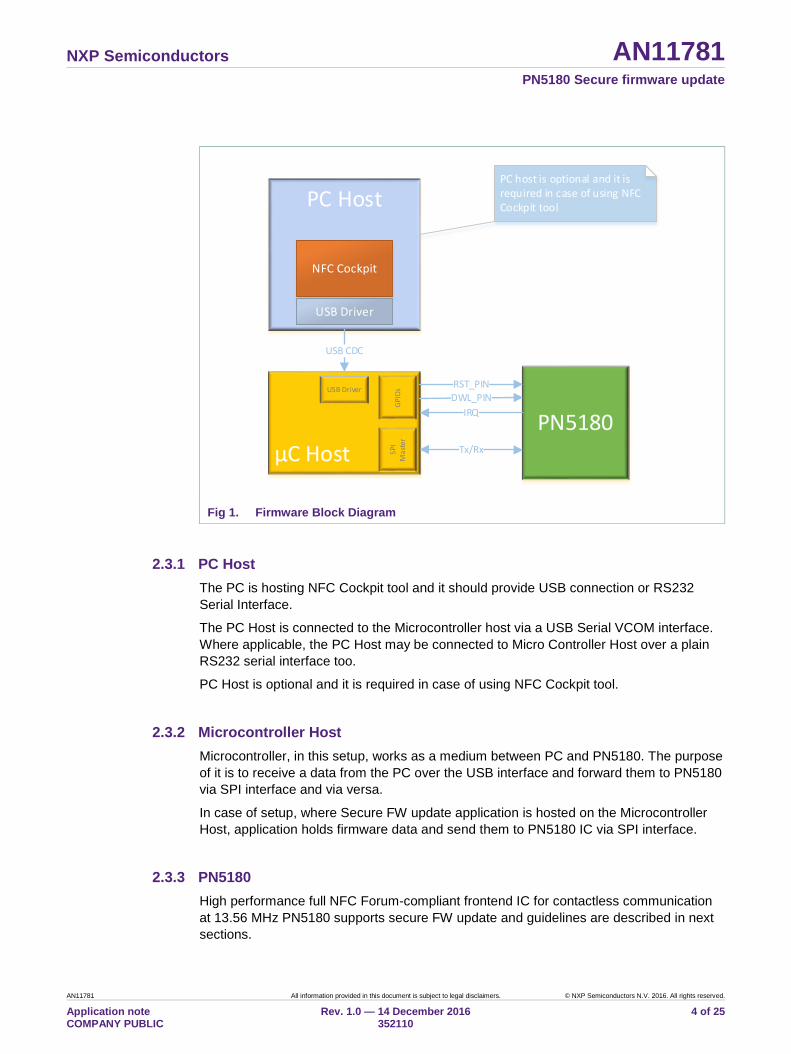
2.3 Block Diagram Overview At a very high level, the system is divided into three parts.
1. PC Host
2. Microcontroller Host
3. PN5180
NXP Semiconductors AN11781 PN5180 Secure firmware update
AN11781 All information provided in this document is subject to legal disclaimers. © NXP Semiconductors N.V. 2016. All rights reserved.
Application note COMPANY PUBLIC
Rev. 1.0 — 14 December 2016 352110
4 of 25
PC Host
NFC Cockpit
µC Host
GPIO
sSP
I M
aste
r
PN5180
RST_PINDWL_PIN
Tx/Rx
USB Driver
USB CDC
IRQ
USB Driver
PC host is optional and it is required in case of using NFC Cockpit tool
Fig 1. Firmware Block Diagram
2.3.1 PC Host The PC is hosting NFC Cockpit tool and it should provide USB connection or RS232 Serial Interface.
The PC Host is connected to the Microcontroller host via a USB Serial VCOM interface. Where applicable, the PC Host may be connected to Micro Controller Host over a plain RS232 serial interface too.
PC Host is optional and it is required in case of using NFC Cockpit tool.
2.3.2 Microcontroller Host Microcontroller, in this setup, works as a medium between PC and PN5180. The purpose of it is to receive a data from the PC over the USB interface and forward them to PN5180 via SPI interface and via versa.
In case of setup, where Secure FW update application is hosted on the Microcontroller Host, application holds firmware data and send them to PN5180 IC via SPI interface.
2.3.3 PN5180 High performance full NFC Forum-compliant frontend IC for contactless communication at 13.56 MHz PN5180 supports secure FW update and guidelines are described in next sections.
NXP Semiconductors AN11781 PN5180 Secure firmware update
AN11781 All information provided in this document is subject to legal disclaimers. © NXP Semiconductors N.V. 2016. All rights reserved.
Application note COMPANY PUBLIC
Rev. 1.0 — 14 December 2016 352110
5 of 25
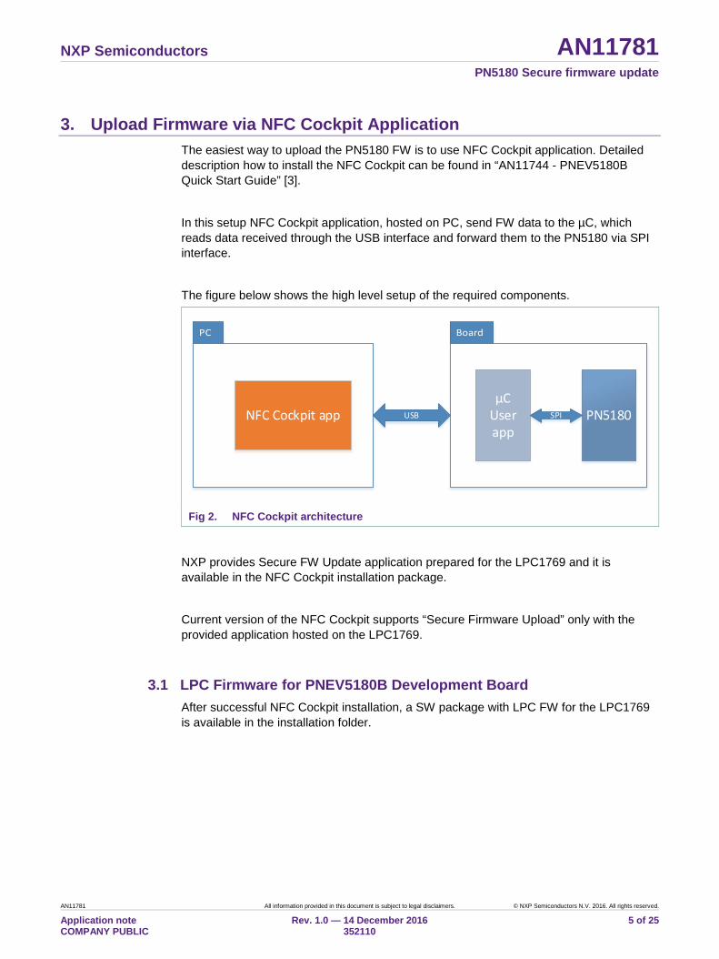
3. Upload Firmware via NFC Cockpit Application The easiest way to upload the PN5180 FW is to use NFC Cockpit application. Detailed description how to install the NFC Cockpit can be found in “AN11744 - PNEV5180B Quick Start Guide” [3].
In this setup NFC Cockpit application, hosted on PC, send FW data to the µC, which reads data received through the USB interface and forward them to the PN5180 via SPI interface.
The figure below shows the high level setup of the required components.
NFC Cockpit appµC
User app
USB PN5180SPI
Fig 2. NFC Cockpit architecture
NXP provides Secure FW Update application prepared for the LPC1769 and it is available in the NFC Cockpit installation package.
Current version of the NFC Cockpit supports “Secure Firmware Upload” only with the provided application hosted on the LPC1769.
3.1 LPC Firmware for PNEV5180B Development Board After successful NFC Cockpit installation, a SW package with LPC FW for the LPC1769 is available in the installation folder.
NXP Semiconductors AN11781 PN5180 Secure firmware update
AN11781 All information provided in this document is subject to legal disclaimers. © NXP Semiconductors N.V. 2016. All rights reserved.
Application note COMPANY PUBLIC
Rev. 1.0 — 14 December 2016 352110
6 of 25
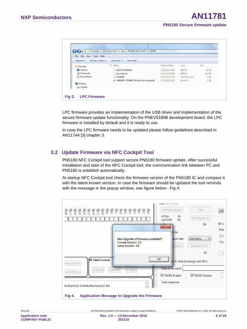
Fig 3. LPC Firmware
LPC firmware provides an implementation of the USB driver and implementation of the secure firmware update functionality. On the PNEV5180B development board, the LPC firmware is installed by default and it is ready to use.
In case the LPC firmware needs to be updated please follow guidelines described in AN11744 [3] chapter 3.
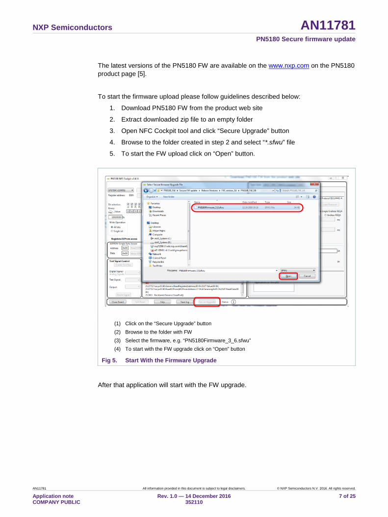
3.2 Update Firmware via NFC Cockpit Tool PN5180 NFC Cockpit tool support secure PN5180 firmware update. After successful installation and start of the NFC Cockpit tool, the communication link between PC and PN5180 is establish automatically.
At startup NFC Cockpit tool check the firmware version of the PN5180 IC and compare it with the latest known version. In case the firmware should be updated the tool reminds with the message in the popup window, see figure below - Fig 4.
Fig 4. Application Message to Upgrade the Firmware
NXP Semiconductors AN11781 PN5180 Secure firmware update
AN11781 All information provided in this document is subject to legal disclaimers. © NXP Semiconductors N.V. 2016. All rights reserved.
Application note COMPANY PUBLIC
Rev. 1.0 — 14 December 2016 352110
7 of 25
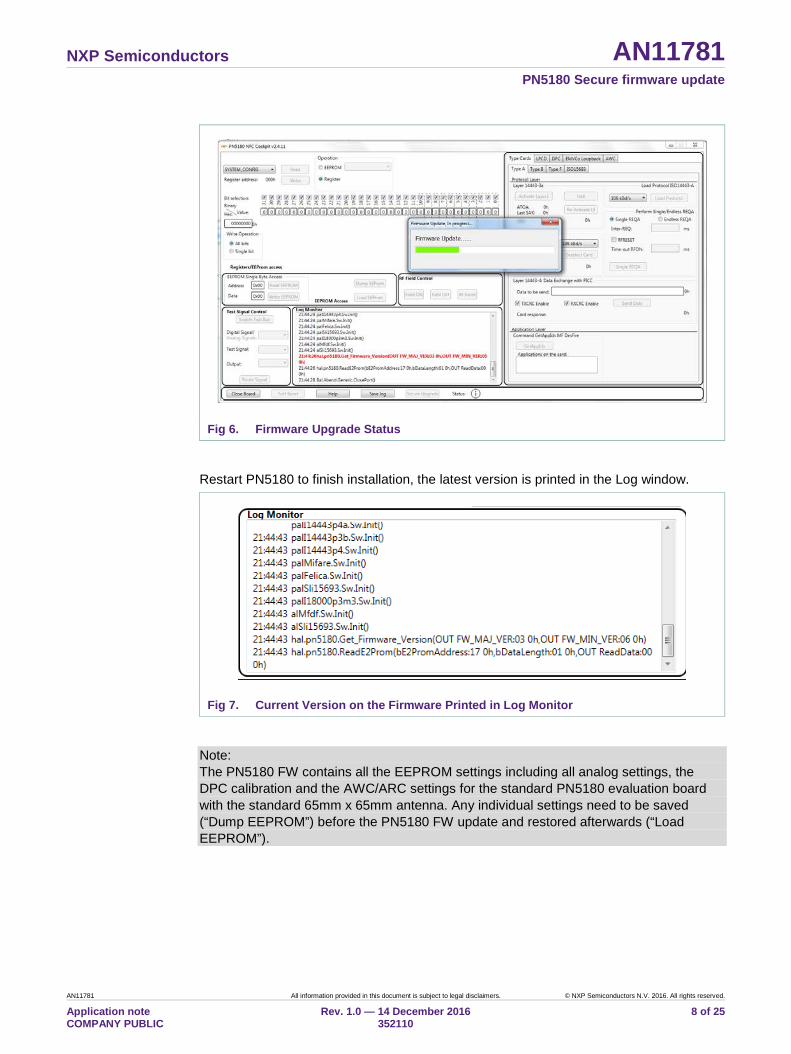
The latest versions of the PN5180 FW are available on the www.nxp.com on the PN5180 product page [5].
To start the firmware upload please follow guidelines described below:
1. Download PN5180 FW from the product web site
2. Extract downloaded zip file to an empty folder
3. Open NFC Cockpit tool and click “Secure Upgrade” button
4. Browse to the folder created in step 2 and select “*.sfwu” file
5. To start the FW upload click on “Open” button.
(1) Click on the “Secure Upgrade” button (2) Browse to the folder with FW (3) Select the firmware, e.g. “PN5180Firmware_3_6.sfwu” (4) To start with the FW upgrade click on “Open” button
Fig 5. Start With the Firmware Upgrade
After that application will start with the FW upgrade.
NXP Semiconductors AN11781 PN5180 Secure firmware update
AN11781 All information provided in this document is subject to legal disclaimers. © NXP Semiconductors N.V. 2016. All rights reserved.
Application note COMPANY PUBLIC
Rev. 1.0 — 14 December 2016 352110
8 of 25
Fig 6. Firmware Upgrade Status
Restart PN5180 to finish installation, the latest version is printed in the Log window.
Fig 7. Current Version on the Firmware Printed in Log Monitor
Note: The PN5180 FW contains all the EEPROM settings including all analog settings, the DPC calibration and the AWC/ARC settings for the standard PN5180 evaluation board with the standard 65mm x 65mm antenna. Any individual settings need to be saved (“Dump EEPROM”) before the PN5180 FW update and restored afterwards (“Load EEPROM”).
NXP Semiconductors AN11781 PN5180 Secure firmware update
AN11781 All information provided in this document is subject to legal disclaimers. © NXP Semiconductors N.V. 2016. All rights reserved.
Application note COMPANY PUBLIC
Rev. 1.0 — 14 December 2016 352110
9 of 25
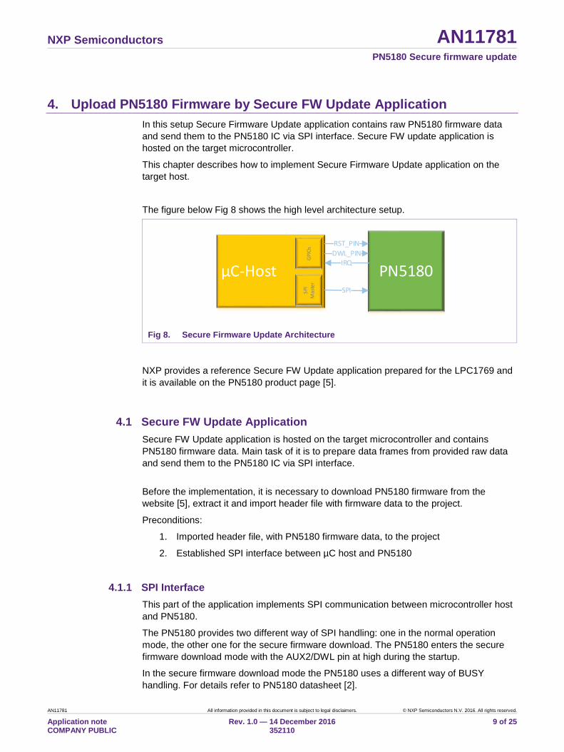
4. Upload PN5180 Firmware by Secure FW Update Application In this setup Secure Firmware Update application contains raw PN5180 firmware data and send them to the PN5180 IC via SPI interface. Secure FW update application is hosted on the target microcontroller.
This chapter describes how to implement Secure Firmware Update application on the target host.
The figure below Fig 8 shows the high level architecture setup.
µC-Host
GPIO
sSP
I M
aste
r
PN5180
RST_PINDWL_PIN
SPI
IRQ
Fig 8. Secure Firmware Update Architecture
NXP provides a reference Secure FW Update application prepared for the LPC1769 and it is available on the PN5180 product page [5].
4.1 Secure FW Update Application Secure FW Update application is hosted on the target microcontroller and contains PN5180 firmware data. Main task of it is to prepare data frames from provided raw data and send them to the PN5180 IC via SPI interface.
Before the implementation, it is necessary to download PN5180 firmware from the website [5], extract it and import header file with firmware data to the project.
Preconditions:
1. Imported header file, with PN5180 firmware data, to the project
2. Established SPI interface between µC host and PN5180
4.1.1 SPI Interface This part of the application implements SPI communication between microcontroller host and PN5180.
The PN5180 provides two different way of SPI handling: one in the normal operation mode, the other one for the secure firmware download. The PN5180 enters the secure firmware download mode with the AUX2/DWL pin at high during the startup.
In the secure firmware download mode the PN5180 uses a different way of BUSY handling. For details refer to PN5180 datasheet [2].
NXP Semiconductors AN11781 PN5180 Secure firmware update
AN11781 All information provided in this document is subject to legal disclaimers. © NXP Semiconductors N.V. 2016. All rights reserved.
Application note COMPANY PUBLIC
Rev. 1.0 — 14 December 2016 352110
10 of 25
To provide this functionality, it is mandatory that “phPlatform” and relevant OSAL and BAL components of the NFC Reader Library [6], are ported to the target platform. To confirm that the NFC Reader library was successfully ported to the target platform, all reference examples, should run without any issue. Porting guidelines of the NXP Reader Library is not part of this documentation.
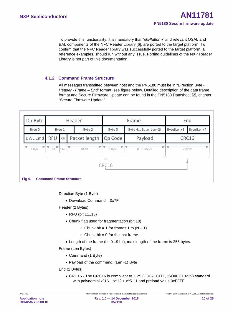
4.1.2 Command Frame Structure All messages transmitted between host and the PN5180 must be in “Direction Byte - Header - Frame – End” format, see figure below. Detailed description of the data frame format and Secure Firmware Update can be found in the PN5180 Datasheet [2], chapter “Secure Firmware Update”.
Byte 1 Byte 2 Byte 3 Byte 4... Byte [Len+2]
RFU Ch Packet length Op Code Payload
Byte[Len+3]
CRC16
Byte[Len+4]
CRC16
Byte 0
Dir Byte
1 Byte 5 bit 1 bit 10 bit 1 Byte (L – 1) Bytes 2 Bytes
DWL Cmd
Header Frame End
Fig 9. Command Frame Structure
Direction Byte (1 Byte)
• Download Command – 0x7F
Header (2 Bytes)
• RFU (bit 11..15)
• Chunk flag used for fragmentation (bit 10)
o Chunk bit = 1 for frames 1 to (N – 1)
o Chunk bit = 0 for the last frame
• Length of the frame (bit 0...9 bit), max length of the frame is 256 bytes.
Frame (Len Bytes)
• Command (1 Byte)
• Payload of the command: (Len -1) Byte
End (2 Bytes)
• CRC16 - The CRC16 is compliant to X.25 (CRC-CCITT, ISO/IEC13239) standard with polynomial x^16 + x^12 + x^5 +1 and preload value 0xFFFF.
NXP Semiconductors AN11781 PN5180 Secure firmware update
AN11781 All information provided in this document is subject to legal disclaimers. © NXP Semiconductors N.V. 2016. All rights reserved.
Application note COMPANY PUBLIC
Rev. 1.0 — 14 December 2016 352110
11 of 25
4.1.3 Supported Commands in Secure Firmware Download Mode Following commands are supported in Secure Firmware Download Mode. Detailed description can be found in PN5180 datasheet [2].
Table 1. Secure Firmware Download Commands Command Comma
nd Code Description
RESET 0xF0 This command resets the PN5180 IC
GET_VERSION 0xF1 This command provides the IC version and firmware version
GET_SESSION_STATE 0xF2 This command provides the session state and lifecycle.
GET_DIE_ID 0xF4 The command returns the die Identifier
CHECK_INTEGRITY 0xE0 This command checks the integrity of components.
SECURE_WRITE 0xC0 Writes chunks of data to the IC
READ 0xA2 This command reads the EEPROM from specified address.
4.1.4 Command Code Response A response message is always a multiple of 4 bytes. The first byte of the response is used to indicate the status of the last executed command.
Table 2. Secure Firmware Command Status Return Codes Command Command Code Description OK 00 command processed properly
ERROR 01 - FF any response different from 0x00 indicates an error
4.1.5 Application Sequence Flow Steps required to send a command in Secure Firmware Download mode:
1. Dump and save all USER EEPROM settings 2. Set DWL_REQ pin on PN5180 to high 3. Reset PN5180 4. The PN1580 boots in download mode 5. Send Command
a. Prepare a data frame b. Wait until BUSY PIN goes LOW c. Send data frame to PN5180 via SPI
6. Read Response 7. Reset PN5180 8. Restore all USER EEPROM settings
In the figure below the high level application flow diagram is presented.
NXP Semiconductors AN11781 PN5180 Secure firmware update
AN11781 All information provided in this document is subject to legal disclaimers. © NXP Semiconductors N.V. 2016. All rights reserved.
Application note COMPANY PUBLIC
Rev. 1.0 — 14 December 2016 352110
12 of 25
µC Host PN5180
RST_PIN Low
DWL_REQ High
RST_PIN High
Wait until Busy goes Low
Send Frame1 byte direction (0x7F)2 byte header1 byte commadN byte payload2 byte CRC16
RST_PIN Low
DWL_RWQ LowRST_PIN High
Command Response
Fig 10. Application Flow Diagram
Note: As Secure FW Update overwrites user EEPROM settings, it is recommended to dump and save EEPROM before firmware update.
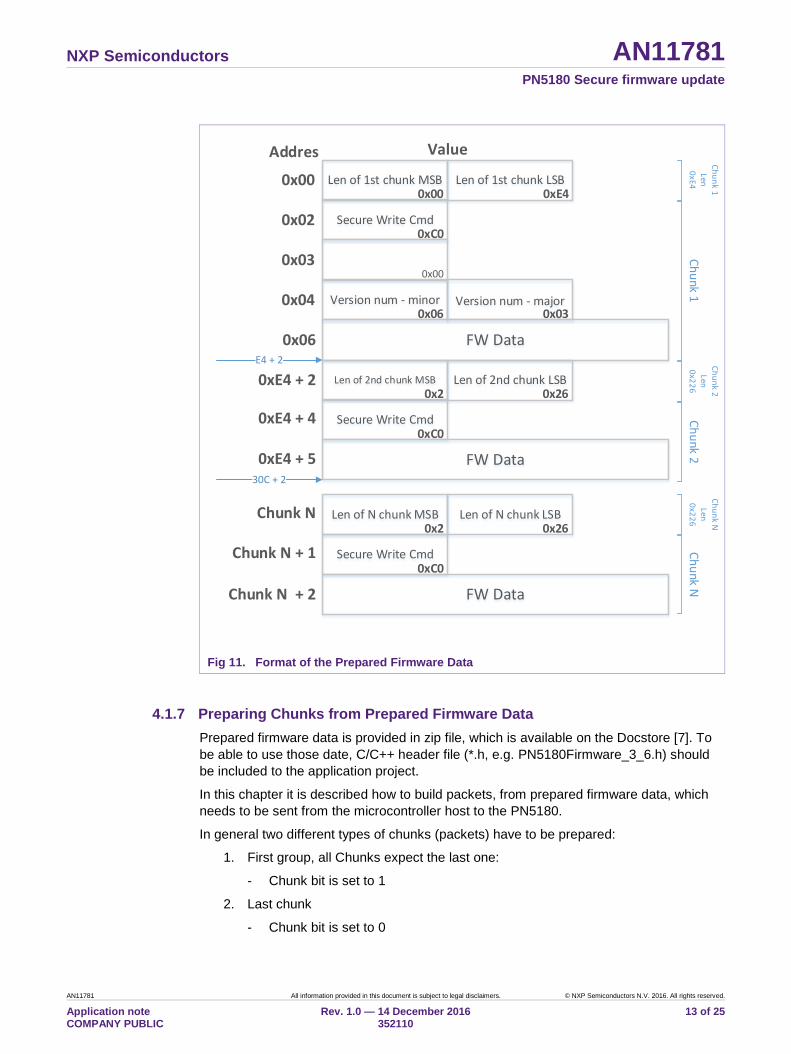
4.1.6 Format of the Prepared Firmware Data NXP provides raw PN5180 firmware data and it is available in the Docstore [7]. Provided data is available as an array of bytes and it should be imported to the Secure Firmware Update application.
Byte array, of the provided firmware, is composed of multiple parts. Each part consists of header and chunk data. Header is 2 byte long and it specifies size of the chunk data. Size of the chunk is arbitrary big. The whole chunk defines the frame data of the “Secure Write” command.
Block diagram below shows structure of the provided firmware.
NXP Semiconductors AN11781 PN5180 Secure firmware update
AN11781 All information provided in this document is subject to legal disclaimers. © NXP Semiconductors N.V. 2016. All rights reserved.
Application note COMPANY PUBLIC
Rev. 1.0 — 14 December 2016 352110
13 of 25
Len of 1st chunk MSB Len of 1st chunk LSB
FW Data
ValueAddres
Secure Write Cmd
0x00
0x02
0x03
Version num - minor Version num - major0x04
0x06
0xC0
0x06 0x03
0x00 0xE4
0x00
Len of 2nd chunk MSB Len of 2nd chunk LSB
0xC0Secure Write Cmd
0x2 0x26
FW Data
Len of N chunk MSB Len of N chunk LSB
0xC0Secure Write Cmd
0x2 0x26
FW Data
0xE4 + 2
0xE4 + 4
0xE4 + 5
Chunk N
Chunk N + 1
Chunk N + 2
E4 + 2
30C + 2
Chunk 1
Chunk 1 Len
0xE4
Chunk 2 Len
0x226Chunk 2
Chunk N
Chunk N
Len 0x226
Fig 11. Format of the Prepared Firmware Data
4.1.7 Preparing Chunks from Prepared Firmware Data Prepared firmware data is provided in zip file, which is available on the Docstore [7]. To be able to use those date, C/C++ header file (*.h, e.g. PN5180Firmware_3_6.h) should be included to the application project.
In this chapter it is described how to build packets, from prepared firmware data, which needs to be sent from the microcontroller host to the PN5180.
In general two different types of chunks (packets) have to be prepared:
1. First group, all Chunks expect the last one:
- Chunk bit is set to 1
2. Last chunk
- Chunk bit is set to 0
NXP Semiconductors AN11781 PN5180 Secure firmware update
AN11781 All information provided in this document is subject to legal disclaimers. © NXP Semiconductors N.V. 2016. All rights reserved.
Application note COMPANY PUBLIC
Rev. 1.0 — 14 December 2016 352110
14 of 25
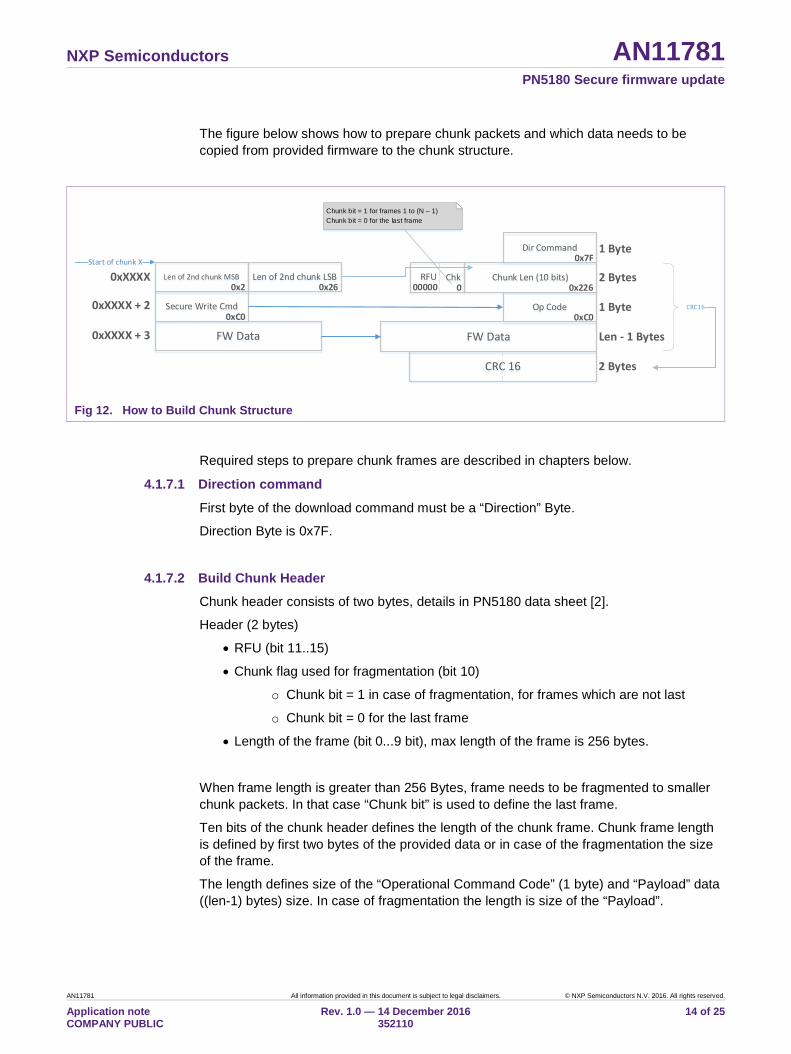
The figure below shows how to prepare chunk packets and which data needs to be copied from provided firmware to the chunk structure.
Len of 2nd chunk MSB Len of 2nd chunk LSB
0xC0Secure Write Cmd
0x2 0x26
FW Data
0xXXXX
0xXXXX + 2
0xXXXX + 3
Start of chunk X
Chunk Len (10 bits)0x226
RFU Chk
Op Code
FW Data
2 Bytes
1 Byte
Len - 1 Bytes
CRC 16 2 Bytes
0xC0CRC16
000000
Dir Command0x7F
1 Byte
Chunk bit = 1 for frames 1 to (N – 1)Chunk bit = 0 for the last frame
Fig 12. How to Build Chunk Structure
Required steps to prepare chunk frames are described in chapters below.
4.1.7.1 Direction command
First byte of the download command must be a “Direction” Byte.
Direction Byte is 0x7F.
4.1.7.2 Build Chunk Header
Chunk header consists of two bytes, details in PN5180 data sheet [2].
Header (2 bytes)
• RFU (bit 11..15)
• Chunk flag used for fragmentation (bit 10)
o Chunk bit = 1 in case of fragmentation, for frames which are not last
o Chunk bit = 0 for the last frame
• Length of the frame (bit 0...9 bit), max length of the frame is 256 bytes.
When frame length is greater than 256 Bytes, frame needs to be fragmented to smaller chunk packets. In that case “Chunk bit” is used to define the last frame.
Ten bits of the chunk header defines the length of the chunk frame. Chunk frame length is defined by first two bytes of the provided data or in case of the fragmentation the size of the frame.
The length defines size of the “Operational Command Code” (1 byte) and “Payload” data ((len-1) bytes) size. In case of fragmentation the length is size of the “Payload”.
NXP Semiconductors AN11781 PN5180 Secure firmware update
AN11781 All information provided in this document is subject to legal disclaimers. © NXP Semiconductors N.V. 2016. All rights reserved.
Application note COMPANY PUBLIC
Rev. 1.0 — 14 December 2016 352110
15 of 25
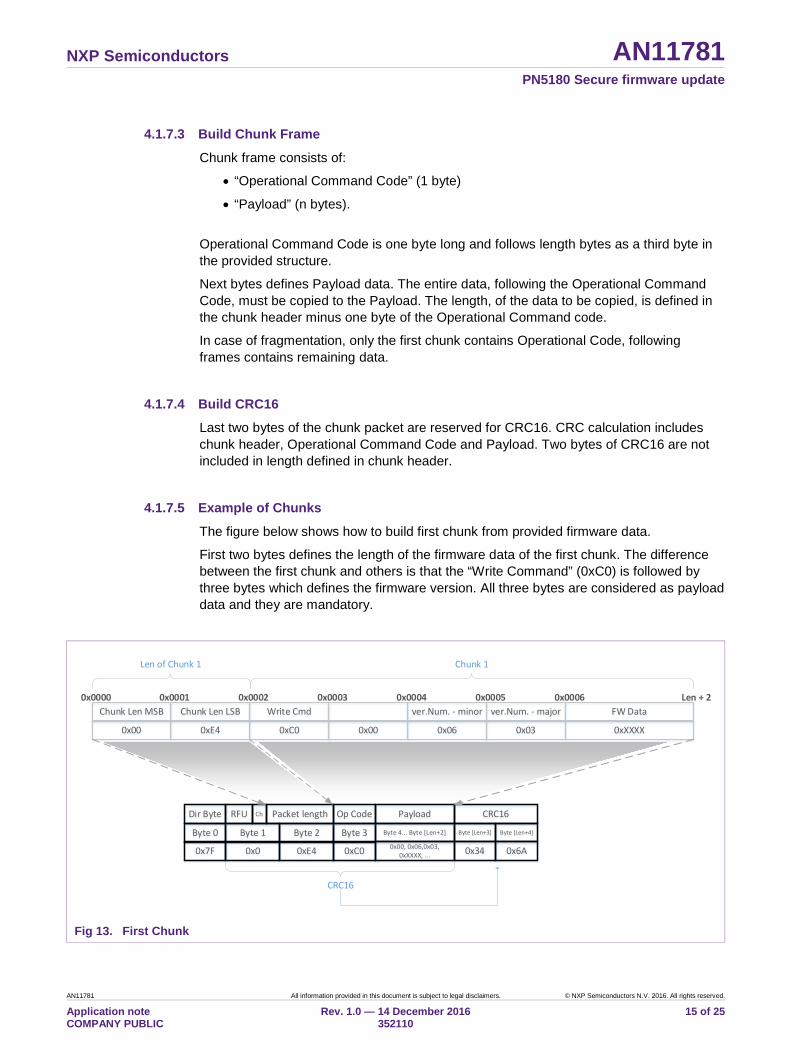
4.1.7.3 Build Chunk Frame
Chunk frame consists of:
• “Operational Command Code” (1 byte)
• “Payload” (n bytes).
Operational Command Code is one byte long and follows length bytes as a third byte in the provided structure.
Next bytes defines Payload data. The entire data, following the Operational Command Code, must be copied to the Payload. The length, of the data to be copied, is defined in the chunk header minus one byte of the Operational Command code.
In case of fragmentation, only the first chunk contains Operational Code, following frames contains remaining data.
4.1.7.4 Build CRC16
Last two bytes of the chunk packet are reserved for CRC16. CRC calculation includes chunk header, Operational Command Code and Payload. Two bytes of CRC16 are not included in length defined in chunk header.
4.1.7.5 Example of Chunks
The figure below shows how to build first chunk from provided firmware data.
First two bytes defines the length of the firmware data of the first chunk. The difference between the first chunk and others is that the “Write Command” (0xC0) is followed by three bytes which defines the firmware version. All three bytes are considered as payload data and they are mandatory.
Byte 1 Byte 2 Byte 3 Byte 4... Byte [Len+2]
0x0 0xE4 0xC0 0x00, 0x06,0x03, 0xXXXX, ...
RFU Ch Packet length Op Code Payload
Chunk Len MSB Chunk Len LSB
0x00 0xE4
Write Cmd ver.Num. - minor ver.Num. - major FW Data
0xC0 0x00 0x06 0x03 0xXXXX
Byte [Len+3]
0x34
CRC16
Byte [Len+4]
0x6A
0x0000 0x0001 0x0002 0x0003 0x0004 0x0005 0x0006 Len + 2
Chunk 1Len of Chunk 1
CRC16
Byte 0
0x7F
Dir Byte
Fig 13. First Chunk
NXP Semiconductors AN11781 PN5180 Secure firmware update
AN11781 All information provided in this document is subject to legal disclaimers. © NXP Semiconductors N.V. 2016. All rights reserved.
Application note COMPANY PUBLIC
Rev. 1.0 — 14 December 2016 352110
16 of 25
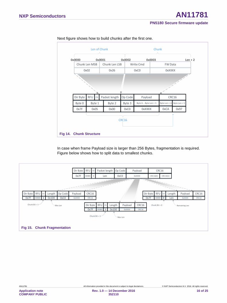
Next figure shows how to build chunks after the first one.
Byte 1 Byte 2 Byte 3 Byte 4... Byte Len + 3
0x05 0x00 0xC0 0xXXXX
RFU Ch Packet length Op Code Payload
Chunk Len MSB Chunk Len LSB
0x02 0x26
Write Cmd FW Data
0xC0 0xXXXX
Byte Len + 4
0xCA
CRC16
Byte Len + 5
0x97
0x0000 0x0001 0x0002 0x0003 Len + 2
ChunkLen of Chunk
CRC16
Byte 0
0x7F
Dir Byte
Fig 14. Chunk Structure
In case when frame Payload size is larger than 256 Bytes, fragmentation is required. Figure below shows how to split data to smallest chunks.
00000 Len 0xC0 0xXXXX
RFU Ch Packet length Op Code Payload
CRC16[0]
CRC16
CRC16[1]0x7F
Dir Byte
0
00000 0x100 0xC0 0xXXXX
RFU Ch Length Op Code PayloadCRC16
CRC160x7F
Dir Byte1
00000 0x100 0xXXXX
RFU Ch Length PayloadCRC16
CRC160x7F
Dir Byte1
00000 Len 0xXXXX
RFU Ch Length PayloadCRC16
CRC160x7F
Dir Byte0
Chunk Bit = 1
Chunk Bit = 1
Chunk Bit = 0Max Len
Max Len
Remaining Len
Fig 15. Chunk Fragmentation
NXP Semiconductors AN11781 PN5180 Secure firmware update
AN11781 All information provided in this document is subject to legal disclaimers. © NXP Semiconductors N.V. 2016. All rights reserved.
Application note COMPANY PUBLIC
Rev. 1.0 — 14 December 2016 352110
17 of 25
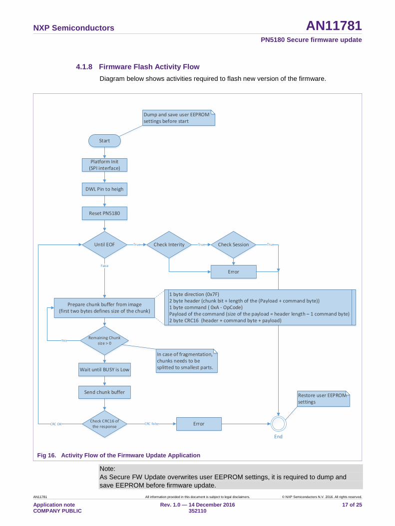
4.1.8 Firmware Flash Activity Flow Diagram below shows activities required to flash new version of the firmware.
Start
DWL Pin to heigh
Reset PN5180
Until EOF
Prepare chunk buffer from image (first two bytes defines size of the chunk)
Wait until BUSY is Low
False
Check InterityTrue Check SessionTrue
Error
End
Platform Init(SPI interface)
1 byte direction (0x7F)2 byte header (chunk bit + length of the (Payload + command byte))1 byte command ( 0xA - OpCode)Payload of the command (size of the payload = header length – 1 command byte)2 byte CRC16 (header + command byte + payload)
Send chunk buffer
Check CRC16 of the responseCRC OK ErrorCRC False
True
Dump and save user EEPROM settings before start
Restore user EEPROM settings
Remaining Chunk size > 0
Yes
In case of fragmentation, chunks needs to be splitted to smallest parts.
Fig 16. Activity Flow of the Firmware Update Application
Note: As Secure FW Update overwrites user EEPROM settings, it is required to dump and save EEPROM before firmware update.
NXP Semiconductors AN11781 PN5180 Secure firmware update
AN11781 All information provided in this document is subject to legal disclaimers. © NXP Semiconductors N.V. 2016. All rights reserved.
Application note COMPANY PUBLIC
Rev. 1.0 — 14 December 2016 352110
18 of 25
4.2 Reference Application NXP provides “DownloadLibEx1” application as a reference example which demonstrates how to flash new firmware by application hosted on the target microcontroller. This example provides implementation of all commands in Secure Firmware Download mode and it can be downloaded from the PN5180 product page [5].
Reference application package is prepared for the LPC1769 platform together with the PN5180B development board and it contains project for the LPCXpresso IDE [4].
Reference example use Secure Download library, which provides implementation of the secure download APIs. It is recommended to use it in the customer application.
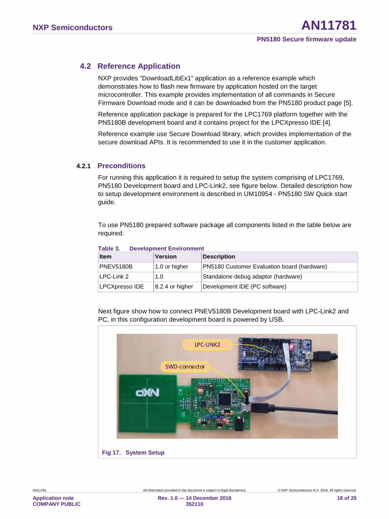
4.2.1 Preconditions
For running this application it is required to setup the system comprising of LPC1769, PN5180 Development board and LPC-Link2, see figure below. Detailed description how to setup development environment is described in UM10954 - PN5180 SW Quick start guide.
To use PN5180 prepared software package all components listed in the table below are required:
Table 3. Development Environment Item Version Description PNEV5180B 1.0 or higher PN5180 Customer Evaluation board (hardware)
LPC-Link 2 1.0 Standalone debug adaptor (hardware)
LPCXpresso IDE 8.2.4 or higher Development IDE (PC software)
Next figure show how to connect PNEV5180B Development board with LPC-Link2 and PC, in this configuration development board is powered by USB.
Fig 17. System Setup
NXP Semiconductors AN11781 PN5180 Secure firmware update
AN11781 All information provided in this document is subject to legal disclaimers. © NXP Semiconductors N.V. 2016. All rights reserved.
Application note COMPANY PUBLIC
Rev. 1.0 — 14 December 2016 352110
19 of 25
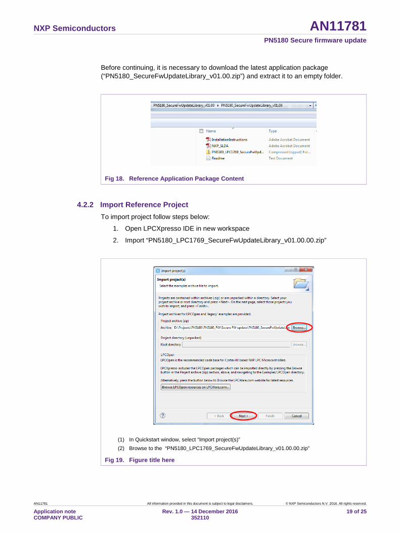
Before continuing, it is necessary to download the latest application package (“PN5180_SecureFwUpdateLibrary_v01.00.zip”) and extract it to an empty folder.
Fig 18. Reference Application Package Content
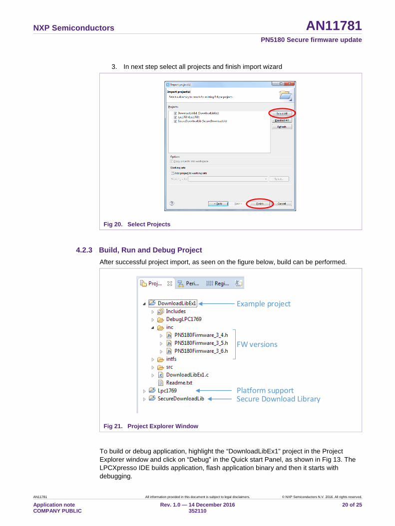
4.2.2 Import Reference Project To import project follow steps below:
1. Open LPCXpresso IDE in new workspace
2. Import “PN5180_LPC1769_SecureFwUpdateLibrary_v01.00.00.zip”
(1) In Quickstart window, select “Import project(s)” (2) Browse to the “PN5180_LPC1769_SecureFwUpdateLibrary_v01.00.00.zip”
Fig 19. Figure title here
NXP Semiconductors AN11781 PN5180 Secure firmware update
AN11781 All information provided in this document is subject to legal disclaimers. © NXP Semiconductors N.V. 2016. All rights reserved.
Application note COMPANY PUBLIC
Rev. 1.0 — 14 December 2016 352110
20 of 25
3. In next step select all projects and finish import wizard
Fig 20. Select Projects
4.2.3 Build, Run and Debug Project After successful project import, as seen on the figure below, build can be performed.
Example project
FW versions
Platform supportSecure Download Library
Fig 21. Project Explorer Window
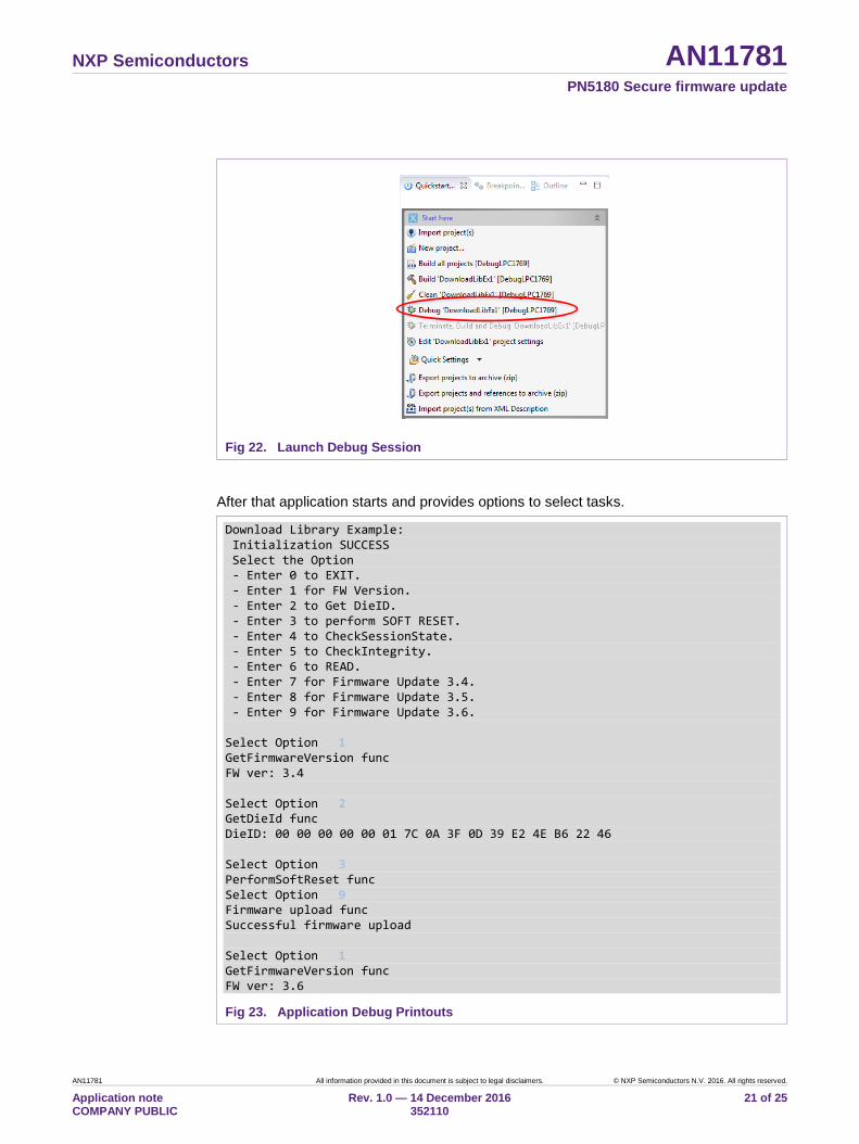
To build or debug application, highlight the “DownloadLibEx1” project in the Project Explorer window and click on “Debug” in the Quick start Panel, as shown in Fig 13. The LPCXpresso IDE builds application, flash application binary and then it starts with debugging.
NXP Semiconductors AN11781 PN5180 Secure firmware update
AN11781 All information provided in this document is subject to legal disclaimers. © NXP Semiconductors N.V. 2016. All rights reserved.
Application note COMPANY PUBLIC
Rev. 1.0 — 14 December 2016 352110
21 of 25
Fig 22. Launch Debug Session
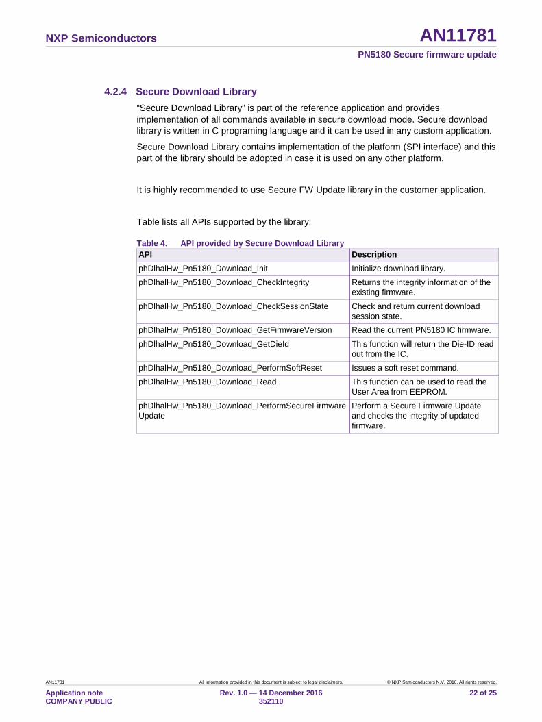
After that application starts and provides options to select tasks.
Download Library Example: Initialization SUCCESS Select the Option - Enter 0 to EXIT. - Enter 1 for FW Version. - Enter 2 to Get DieID. - Enter 3 to perform SOFT RESET. - Enter 4 to CheckSessionState. - Enter 5 to CheckIntegrity. - Enter 6 to READ. - Enter 7 for Firmware Update 3.4. - Enter 8 for Firmware Update 3.5. - Enter 9 for Firmware Update 3.6. Select Option 1 GetFirmwareVersion func FW ver: 3.4 Select Option 2 GetDieId func DieID: 00 00 00 00 00 01 7C 0A 3F 0D 39 E2 4E B6 22 46 Select Option 3 PerformSoftReset func Select Option 9 Firmware upload func Successful firmware upload Select Option 1 GetFirmwareVersion func FW ver: 3.6
Fig 23. Application Debug Printouts
NXP Semiconductors AN11781 PN5180 Secure firmware update
AN11781 All information provided in this document is subject to legal disclaimers. © NXP Semiconductors N.V. 2016. All rights reserved.
Application note COMPANY PUBLIC
Rev. 1.0 — 14 December 2016 352110
22 of 25
4.2.4 Secure Download Library “Secure Download Library” is part of the reference application and provides implementation of all commands available in secure download mode. Secure download library is written in C programing language and it can be used in any custom application.
Secure Download Library contains implementation of the platform (SPI interface) and this part of the library should be adopted in case it is used on any other platform.
It is highly recommended to use Secure FW Update library in the customer application.
Table lists all APIs supported by the library:
Table 4. API provided by Secure Download Library API Description phDlhalHw_Pn5180_Download_Init Initialize download library.
phDlhalHw_Pn5180_Download_CheckIntegrity Returns the integrity information of the existing firmware.
phDlhalHw_Pn5180_Download_CheckSessionState Check and return current download session state.
phDlhalHw_Pn5180_Download_GetFirmwareVersion Read the current PN5180 IC firmware.
phDlhalHw_Pn5180_Download_GetDieId This function will return the Die-ID read out from the IC.
phDlhalHw_Pn5180_Download_PerformSoftReset Issues a soft reset command.
phDlhalHw_Pn5180_Download_Read This function can be used to read the User Area from EEPROM.
phDlhalHw_Pn5180_Download_PerformSecureFirmwareUpdate
Perform a Secure Firmware Update and checks the integrity of updated firmware.
NXP Semiconductors AN11781 PN5180 Secure firmware update
AN11781 All information provided in this document is subject to legal disclaimers. © NXP Semiconductors N.V. 2016. All rights reserved.
Application note COMPANY PUBLIC
Rev. 1.0 — 14 December 2016 352110
23 of 25
5. References [1] OM25180FDK – PN5180 development kit
[2] PN5180 datasheet, www.nxp.com
[3] AN11744 PNEV5180B Quick Start Guide
[4] LPCXpresso IDE - http://www.nxp.com/products/software-and-tools/software-development-tools/software-tools/lpc-microcontroller-utilities/lpcxpresso-ide-v8.2.2:LPCXPRESSO
[5] Product page of the PN5180 http://www.nxp.com/products/identification-and-security/nfc-and-reader-ics/nfc-frontend-solutions/high-performance-multi-protocol-full-nfc-forum-compliant-frontend:PN5180
[6] NFC Reader Library - Software support for NFC Frontend solutions http://www.nxp.com/products/identification-and-security/nfc-and-reader-ics/nfc-controller-solutions/nfc-reader-library-software-support-for-nfc-frontend-solutions:NFC-READER-LIBRARY
[7] PN5180 docstore folder https://www.docstore.nxp.com/flex/DocStoreApp.html#/p//Reader-ICs/Infrastructure-NFC-Ctless-SAM/PN5180
NXP Semiconductors AN11781 PN5180 Secure firmware update
AN11781 All information provided in this document is subject to legal disclaimers. © NXP Semiconductors N.V. 20164. All rights reserved.
Application note COMPANY PUBLIC
Rev. 1.0 — 14 December 2016 352110
24 of 25
6. Legal information
6.1 Definitions Draft — The document is a draft version only. The content is still under internal review and subject to formal approval, which may result in modifications or additions. NXP Semiconductors does not give any representations or warranties as to the accuracy or completeness of information included herein and shall have no liability for the consequences of use of such information.
6.2 Disclaimers Limited warranty and liability — Information in this document is believed to be accurate and reliable. However, NXP Semiconductors does not give any representations or warranties, expressed or implied, as to the accuracy or completeness of such information and shall have no liability for the consequences of use of such information. NXP Semiconductors takes no responsibility for the content in this document if provided by an information source outside of NXP Semiconductors.
In no event shall NXP Semiconductors be liable for any indirect, incidental, punitive, special or consequential damages (including - without limitation - lost profits, lost savings, business interruption, costs related to the removal or replacement of any products or rework charges) whether or not such damages are based on tort (including negligence), warranty, breach of contract or any other legal theory.
Notwithstanding any damages that customer might incur for any reason whatsoever, NXP Semiconductors’ aggregate and cumulative liability towards customer for the products described herein shall be limited in accordance with the Terms and conditions of commercial sale of NXP Semiconductors.
Right to make changes — NXP Semiconductors reserves the right to make changes to information published in this document, including without limitation specifications and product descriptions, at any time and without notice. This document supersedes and replaces all information supplied prior to the publication hereof.
Suitability for use — NXP Semiconductors products are not designed, authorized or warranted to be suitable for use in life support, life-critical or safety-critical systems or equipment, nor in applications where failure or malfunction of an NXP Semiconductors product can reasonably be expected to result in personal injury, death or severe property or environmental damage. NXP Semiconductors and its suppliers accept no liability for inclusion and/or use of NXP Semiconductors products in such equipment or applications and therefore such inclusion and/or use is at the customer’s own risk.
Applications — Applications that are described herein for any of these products are for illustrative purposes only. NXP Semiconductors makes no representation or warranty that such applications will be suitable for the specified use without further testing or modification.
Customers are responsible for the design and operation of their applications and products using NXP Semiconductors products, and NXP Semiconductors accepts no liability for any assistance with applications or customer product design. It is customer’s sole responsibility to determine whether the NXP Semiconductors product is suitable and fit for the customer’s applications and products planned, as well as for the planned application and use of customer’s third party customer(s). Customers should provide appropriate design and operating safeguards to minimize the risks associated with their applications and products.
NXP Semiconductors does not accept any liability related to any default, damage, costs or problem which is based on any weakness or default in the customer’s applications or products, or the application or use by customer’s third party customer(s). Customer is responsible for doing all necessary testing for the customer’s applications and products using NXP Semiconductors products in order to avoid a default of the applications and the products or of the application or use by customer’s third party customer(s). NXP does not accept any liability in this respect.
Export control — This document as well as the item(s) described herein may be subject to export control regulations. Export might require a prior authorization from competent authorities.
Translations — A non-English (translated) version of a document is for reference only. The English version shall prevail in case of any discrepancy between the translated and English versions.
Evaluation products — This product is provided on an “as is” and “with all faults” basis for evaluation purposes only. NXP Semiconductors, its affiliates and their suppliers expressly disclaim all warranties, whether express, implied or statutory, including but not limited to the implied warranties of non-infringement, merchantability and fitness for a particular purpose. The entire risk as to the quality, or arising out of the use or performance, of this product remains with customer.
In no event shall NXP Semiconductors, its affiliates or their suppliers be liable to customer for any special, indirect, consequential, punitive or incidental damages (including without limitation damages for loss of business, business interruption, loss of use, loss of data or information, and the like) arising out the use of or inability to use the product, whether or not based on tort (including negligence), strict liability, breach of contract, breach of warranty or any other theory, even if advised of the possibility of such damages.
Notwithstanding any damages that customer might incur for any reason whatsoever (including without limitation, all damages referenced above and all direct or general damages), the entire liability of NXP Semiconductors, its affiliates and their suppliers and customer’s exclusive remedy for all of the foregoing shall be limited to actual damages incurred by customer based on reasonable reliance up to the greater of the amount actually paid by customer for the product or five dollars (US$5.00). The foregoing limitations, exclusions and disclaimers shall apply to the maximum extent permitted by applicable law, even if any remedy fails of its essential purpose.
6.3 Licenses Purchase of NXP ICs with NFC technology
Purchase of an NXP Semiconductors IC that complies with one of the Near Field Communication (NFC) standards ISO/IEC 18092 and ISO/IEC 21481 does not convey an implied license under any patent right infringed by implementation of any of those standards. Purchase of NXP Semiconductors IC does not include a license to any NXP patent (or other IP right) covering combinations of those products with other products, whether hardware or software.
6.4 Trademarks Notice: All referenced brands, product names, service names and trademarks are property of their respective owners.
MIFARE — is a trademark of NXP B.V.
NXP Semiconductors AN11781 PN5180 Secure firmware update
Please be aware that important notices concerning this document and the product(s) described herein, have been included in the section 'Legal information'.
© NXP Semiconductors N.V. 2016. All rights reserved.
For more information, visit: http://www.nxp.com
Date of release: 14 December 2016 352110
Document identifier: AN11781
7. Contents
1. Introduction ......................................................... 3 2. Getting started ..................................................... 3 2.1 System requirements ......................................... 3 2.2 Hardware requirements ...................................... 3 2.3 Block Diagram Overview .................................... 3 2.3.1 PC Host .............................................................. 4 2.3.2 Microcontroller Host ........................................... 4 2.3.3 PN5180 .............................................................. 4 3. Upload Firmware via NFC Cockpit Application 5 3.1 LPC Firmware for PNEV5180B Development
Board ................................................................. 5 3.2 Update Firmware via NFC Cockpit Tool ............. 6 4. Upload PN5180 Firmware by Secure FW Update
Application ........................................................... 9 4.1 Secure FW Update Application .......................... 9 4.1.1 SPI Interface ...................................................... 9 4.1.2 Command Frame Structure .............................. 10 4.1.3 Supported Commands in Secure Firmware
Download Mode ............................................... 11 4.1.4 Command Code Response .............................. 11 4.1.5 Application Sequence Flow .............................. 11 4.1.6 Format of the Prepared Firmware Data ............ 12 4.1.7 Preparing Chunks from Prepared Firmware
Data ................................................................. 13 4.1.7.1 Direction command .......................................... 14 4.1.7.2 Build Chunk Header ......................................... 14 4.1.7.3 Build Chunk Frame .......................................... 15 4.1.7.4 Build CRC16 .................................................... 15 4.1.7.5 Example of Chunks .......................................... 15 4.1.8 Firmware Flash Activity Flow ............................ 17 4.2 Reference Application ...................................... 18 4.2.1 Preconditions ................................................... 18 4.2.2 Import Reference Project ................................. 19 4.2.3 Build, Run and Debug Project .......................... 20 4.2.4 Secure Download Library ................................. 22 5. References ......................................................... 23 6. Legal information .............................................. 24 6.1 Definitions ........................................................ 24 6.2 Disclaimers....................................................... 24 6.3 Licenses ........................................................... 24 6.4 Trademarks ...................................................... 24 7. Contents ............................................................. 25