an2010-10 - hybrid kit for hybridpack™2
TRANSCRIPT

System Engineer ing
Appl icat ion Note
V2.4, 2014-08-11
Hybr id Ki t for Hybr idPACK™2
Evaluat ion Ki t for Appl icat ions wi th Hybr idPACK™2 Module
Hybr idPACK™

Edition 2014-08-11Published byInfineon Technologies AG81726 Munich, Germany© 2014 Infineon Technologies AGAll Rights Reserved.
Legal DisclaimerThe information given in this document shall in no event be regarded as a guarantee of conditions or characteristics. With respect to any examples or hints given herein, any typical values stated herein and/or any information regarding the application of the device, Infineon Technologies hereby disclaims any and all warranties and liabilities of any kind, including without limitation, warranties of non-infringement of intellectual property rights of any third party.
InformationFor further information on technology, delivery terms and conditions and prices, please contact the nearest Infineon Technologies Office (www.infineon.com).
WarningsDue to technical requirements, components may contain dangerous substances. For information on the types in question, please contact the nearest Infineon Technologies Office.Infineon Technologies components may be used in life-support devices or systems only with the express written approval of Infineon Technologies, if a failure of such components can reasonably be expected to cause the failure of that life-support device or system or to affect the safety or effectiveness of that device or system. Life support devices or systems are intended to be implanted in the human body or to support and/or maintain and sustain and/or protect human life. If they fail, it is reasonable to assume that the health of the user or other persons may be endangered.

Hybrid Kit for HybridPACK™2Evaluation Kit for Applications with HybridPACK™2 Module
Application Note 3 V2.4, 2014-08-11
Trademarks of Infineon Technologies AGA-GOLD™, BlueMoon™, COMNEON™, CONVERGATE™, COSIC™, C166™, CROSSAVE™, CanPAK™,CIPOS™, CoolMOS™, CoolSET™, CONVERPATH™, CORECONTROL™, DAVE™, DUALFALC™, DUSLIC™,EasyPIM™, EconoBRIDGE™, EconoDUAL™, EconoPACK™, EconoPIM™, E-GOLD™, EiceDRIVER™,EUPEC™, ELIC™, EPIC™, FALC™, FCOS™, FLEXISLIC™, GEMINAX™, GOLDMOS™, HITFET™,HybridPACK™, INCA™, ISAC™, ISOFACE™, IsoPACK™, IWORX™, M-GOLD™, MIPAQ™, ModSTACK™,MUSLIC™, my-d™, NovalithIC™, OCTALFALC™, OCTAT™, OmniTune™, OmniVia™, OptiMOS™,OPTIVERSE™, ORIGA™, PROFET™, PRO-SIL™, PrimePACK™, QUADFALC™, RASIC™, ReverSave™,SatRIC™, SCEPTRE™, SCOUT™, S-GOLD™, SensoNor™, SEROCCO™, SICOFI™, SIEGET™,SINDRION™, SLIC™, SMARTi™, SmartLEWIS™, SMINT™, SOCRATES™, TEMPFET™, thinQ!™,TrueNTRY™, TriCore™, TRENCHSTOP™, VINAX™, VINETIC™, VIONTIC™, WildPass™, X-GOLD™, XMM™,X-PMU™, XPOSYS™, XWAY™.
Other TrademarksAMBA™, ARM™, MULTI-ICE™, PRIMECELL™, REALVIEW™, THUMB™ of ARM Limited, UK. AUTOSAR™ islicensed by AUTOSAR development partnership. Bluetooth™ of Bluetooth SIG Inc. CAT-iq™ of DECT Forum.COLOSSUS™, FirstGPS™ of Trimble Navigation Ltd. EMV™ of EMVCo, LLC (Visa Holdings Inc.). EPCOS™ ofEpcos AG. FLEXGO™ of Microsoft Corporation. FlexRay™ is licensed by FlexRay Consortium.HYPERTERMINAL™ of Hilgraeve Incorporated. IEC™ of Commission Electrotechnique Internationale. IrDA™ ofInfrared Data Association Corporation. ISO™ of INTERNATIONAL ORGANIZATION FOR STANDARDIZATION.MATLAB™ of MathWorks, Inc. MAXIM™ of Maxim Integrated Products, Inc. MICROTEC™, NUCLEUS™ ofMentor Graphics Corporation. Mifare™ of NXP. MIPI™ of MIPI Alliance, Inc. MIPS™ of MIPS Technologies, Inc.,USA. muRata™ of MURATA MANUFACTURING CO. OmniVision™ of OmniVision Technologies, Inc.Openwave™ Openwave Systems Inc. RED HAT™ Red Hat, Inc. RFMD™ RF Micro Devices, Inc. SIRIUS™ ofSirius Sattelite Radio Inc. SOLARIS™ of Sun Microsystems, Inc. SPANSION™ of Spansion LLC Ltd. Symbian™of Symbian Software Limited. TAIYO YUDEN™ of Taiyo Yuden Co. TEAKLITE™ of CEVA, Inc. TEKTRONIX™of Tektronix Inc. TOKO™ of TOKO KABUSHIKI KAISHA TA. UNIX™ of X/Open Company Limited. VERILOG™,PALLADIUM™ of Cadence Design Systems, Inc. VLYNQ™ of Texas Instruments Incorporated. VXWORKS™,WIND RIVER™ of WIND RIVER SYSTEMS, INC. ZETEX™ of Diodes Zetex Limited.Last Trademarks Update 2009-10-19
Hybrid Kit for HybridPACK™2 Revision History: 2014-08-11, V2.4Previous Revision: V2.3Page Subjects (major changes since last revision)36 Figure 29, changed capacitors C875 (from 22uF to 4.5uF) and C876 (from 22uF to 100uF)48 Figure 3, changed capacitors C875 (from 22uF to 4.5uF) and C876 (from 22uF to 100uF)

Hybrid Kit for HybridPACK™2Evaluation Kit for Applications with HybridPACK™2 Module
Table of Contents
Application Note 4 V2.4, 2014-08-11
Table of Contents . . . . . . . . . . . . . . . . . . . . . . . . . . . . . . . . . . . . . . . . . . . . . . . . . . . . . . . . . . . . . . . . 4
List of Figures . . . . . . . . . . . . . . . . . . . . . . . . . . . . . . . . . . . . . . . . . . . . . . . . . . . . . . . . . . . . . . . . . . . 6
List of Tables . . . . . . . . . . . . . . . . . . . . . . . . . . . . . . . . . . . . . . . . . . . . . . . . . . . . . . . . . . . . . . . . . . . . 8
1 Introduction . . . . . . . . . . . . . . . . . . . . . . . . . . . . . . . . . . . . . . . . . . . . . . . . . . . . . . . . . . . . . . . . . . . . 101.1 How to Order Hybrid Kit for HybridPACK™2 . . . . . . . . . . . . . . . . . . . . . . . . . . . . . . . . . . . . . . . . . . . 10
2 Design Features . . . . . . . . . . . . . . . . . . . . . . . . . . . . . . . . . . . . . . . . . . . . . . . . . . . . . . . . . . . . . . . . 122.1 Main Features . . . . . . . . . . . . . . . . . . . . . . . . . . . . . . . . . . . . . . . . . . . . . . . . . . . . . . . . . . . . . . . . . . . 122.2 Dimensions . . . . . . . . . . . . . . . . . . . . . . . . . . . . . . . . . . . . . . . . . . . . . . . . . . . . . . . . . . . . . . . . . . . . . 132.3 Key Components . . . . . . . . . . . . . . . . . . . . . . . . . . . . . . . . . . . . . . . . . . . . . . . . . . . . . . . . . . . . . . . . 132.3.1 Driver Board (6ED100HP2-FA) . . . . . . . . . . . . . . . . . . . . . . . . . . . . . . . . . . . . . . . . . . . . . . . . . . . . 132.3.2 Logic Board . . . . . . . . . . . . . . . . . . . . . . . . . . . . . . . . . . . . . . . . . . . . . . . . . . . . . . . . . . . . . . . . . . . 142.3.3 HybridPACK™2 . . . . . . . . . . . . . . . . . . . . . . . . . . . . . . . . . . . . . . . . . . . . . . . . . . . . . . . . . . . . . . . . 142.3.4 DC-Link Capacitor . . . . . . . . . . . . . . . . . . . . . . . . . . . . . . . . . . . . . . . . . . . . . . . . . . . . . . . . . . . . . . 152.3.5 Cooling Element . . . . . . . . . . . . . . . . . . . . . . . . . . . . . . . . . . . . . . . . . . . . . . . . . . . . . . . . . . . . . . . 16
3 Hybrid Kit for the HybridPACK™2 Evaluation Driver Board . . . . . . . . . . . . . . . . . . . . . . . . . . . . 193.1 Main Features . . . . . . . . . . . . . . . . . . . . . . . . . . . . . . . . . . . . . . . . . . . . . . . . . . . . . . . . . . . . . . . . . . . 193.2 Key Data . . . . . . . . . . . . . . . . . . . . . . . . . . . . . . . . . . . . . . . . . . . . . . . . . . . . . . . . . . . . . . . . . . . . . . . 203.3 External Connector Pin Assignment . . . . . . . . . . . . . . . . . . . . . . . . . . . . . . . . . . . . . . . . . . . . . . . . . . 213.4 Mechanical Dimensions of the Driver Board . . . . . . . . . . . . . . . . . . . . . . . . . . . . . . . . . . . . . . . . . . . . 223.5 Operation of the Driver Board . . . . . . . . . . . . . . . . . . . . . . . . . . . . . . . . . . . . . . . . . . . . . . . . . . . . . . . 233.5.1 Switching Mode Power Supply (SMPS) . . . . . . . . . . . . . . . . . . . . . . . . . . . . . . . . . . . . . . . . . . . . . . 233.5.2 Input Logic . . . . . . . . . . . . . . . . . . . . . . . . . . . . . . . . . . . . . . . . . . . . . . . . . . . . . . . . . . . . . . . . . . . . 233.5.3 IGBT Switch-off Behavior . . . . . . . . . . . . . . . . . . . . . . . . . . . . . . . . . . . . . . . . . . . . . . . . . . . . . . . . 243.5.4 Maximum Switching Frequency . . . . . . . . . . . . . . . . . . . . . . . . . . . . . . . . . . . . . . . . . . . . . . . . . . . 253.5.5 Booster . . . . . . . . . . . . . . . . . . . . . . . . . . . . . . . . . . . . . . . . . . . . . . . . . . . . . . . . . . . . . . . . . . . . . . 263.5.6 Short Circuit Protection and Clamp Function . . . . . . . . . . . . . . . . . . . . . . . . . . . . . . . . . . . . . . . . . . 273.5.7 Fault Output . . . . . . . . . . . . . . . . . . . . . . . . . . . . . . . . . . . . . . . . . . . . . . . . . . . . . . . . . . . . . . . . . . . 293.5.8 Temperature Measurement . . . . . . . . . . . . . . . . . . . . . . . . . . . . . . . . . . . . . . . . . . . . . . . . . . . . . . . 303.5.9 DC Voltage Measurement . . . . . . . . . . . . . . . . . . . . . . . . . . . . . . . . . . . . . . . . . . . . . . . . . . . . . . . . 303.6 Switching Losses . . . . . . . . . . . . . . . . . . . . . . . . . . . . . . . . . . . . . . . . . . . . . . . . . . . . . . . . . . . . . . . . 313.7 Definition of Layers of Driver Board . . . . . . . . . . . . . . . . . . . . . . . . . . . . . . . . . . . . . . . . . . . . . . . . . . 313.8 Schematics, Layout and Bill of Material . . . . . . . . . . . . . . . . . . . . . . . . . . . . . . . . . . . . . . . . . . . . . . . 323.8.1 Schematics . . . . . . . . . . . . . . . . . . . . . . . . . . . . . . . . . . . . . . . . . . . . . . . . . . . . . . . . . . . . . . . . . . . 323.8.2 Assembly Drawing . . . . . . . . . . . . . . . . . . . . . . . . . . . . . . . . . . . . . . . . . . . . . . . . . . . . . . . . . . . . . . 393.8.3 Layout . . . . . . . . . . . . . . . . . . . . . . . . . . . . . . . . . . . . . . . . . . . . . . . . . . . . . . . . . . . . . . . . . . . . . . . 433.8.4 Bill of Materials . . . . . . . . . . . . . . . . . . . . . . . . . . . . . . . . . . . . . . . . . . . . . . . . . . . . . . . . . . . . . . . . 45
4 Hybrid Kit for the HybridPACK™2 Logic Board . . . . . . . . . . . . . . . . . . . . . . . . . . . . . . . . . . . . . . 484.1 External Connector Pin Assignment . . . . . . . . . . . . . . . . . . . . . . . . . . . . . . . . . . . . . . . . . . . . . . . . . . 514.2 Connector to the Driver Board (K1) . . . . . . . . . . . . . . . . . . . . . . . . . . . . . . . . . . . . . . . . . . . . . . . . . . 554.3 Power Supply . . . . . . . . . . . . . . . . . . . . . . . . . . . . . . . . . . . . . . . . . . . . . . . . . . . . . . . . . . . . . . . . . . . 554.4 Microcontroller . . . . . . . . . . . . . . . . . . . . . . . . . . . . . . . . . . . . . . . . . . . . . . . . . . . . . . . . . . . . . . . . . . 564.4.1 Configuration of TC1767 . . . . . . . . . . . . . . . . . . . . . . . . . . . . . . . . . . . . . . . . . . . . . . . . . . . . . . . . . 564.4.1.1 Boot Configuration of TC1767 . . . . . . . . . . . . . . . . . . . . . . . . . . . . . . . . . . . . . . . . . . . . . . . . . . . 564.4.1.2 Selecting Serial/Parallel Interface . . . . . . . . . . . . . . . . . . . . . . . . . . . . . . . . . . . . . . . . . . . . . . . . 574.5 Watchdog . . . . . . . . . . . . . . . . . . . . . . . . . . . . . . . . . . . . . . . . . . . . . . . . . . . . . . . . . . . . . . . . . . . . . . 584.6 Phase Current Sensing . . . . . . . . . . . . . . . . . . . . . . . . . . . . . . . . . . . . . . . . . . . . . . . . . . . . . . . . . . . . 58
Table of Contents

Hybrid Kit for HybridPACK™2Evaluation Kit for Applications with HybridPACK™2 Module
Table of Contents
Application Note 5 V2.4, 2014-08-11
4.7 Resolver Interface . . . . . . . . . . . . . . . . . . . . . . . . . . . . . . . . . . . . . . . . . . . . . . . . . . . . . . . . . . . . . . . . 584.8 Encoder Interface . . . . . . . . . . . . . . . . . . . . . . . . . . . . . . . . . . . . . . . . . . . . . . . . . . . . . . . . . . . . . . . . 584.9 Hall Sensor Interface . . . . . . . . . . . . . . . . . . . . . . . . . . . . . . . . . . . . . . . . . . . . . . . . . . . . . . . . . . . . . 584.10 GMR Interface . . . . . . . . . . . . . . . . . . . . . . . . . . . . . . . . . . . . . . . . . . . . . . . . . . . . . . . . . . . . . . . . . . 594.10.1 GMR SSC Interface Mode . . . . . . . . . . . . . . . . . . . . . . . . . . . . . . . . . . . . . . . . . . . . . . . . . . . . . . . . 594.10.2 GMR Encoder Interface Mode . . . . . . . . . . . . . . . . . . . . . . . . . . . . . . . . . . . . . . . . . . . . . . . . . . . . . 614.10.3 GMR Hall Sensor Interface Mode . . . . . . . . . . . . . . . . . . . . . . . . . . . . . . . . . . . . . . . . . . . . . . . . . . 614.11 Definition of Layers for the Logic Board . . . . . . . . . . . . . . . . . . . . . . . . . . . . . . . . . . . . . . . . . . . . . . . 614.12 Schematics, Layout and Bill of Materials . . . . . . . . . . . . . . . . . . . . . . . . . . . . . . . . . . . . . . . . . . . . . . 624.12.1 Schematics . . . . . . . . . . . . . . . . . . . . . . . . . . . . . . . . . . . . . . . . . . . . . . . . . . . . . . . . . . . . . . . . . . . 624.12.2 Assembly Drawing . . . . . . . . . . . . . . . . . . . . . . . . . . . . . . . . . . . . . . . . . . . . . . . . . . . . . . . . . . . . . . 764.12.3 Layout . . . . . . . . . . . . . . . . . . . . . . . . . . . . . . . . . . . . . . . . . . . . . . . . . . . . . . . . . . . . . . . . . . . . . . . 804.12.4 Bill of Materials . . . . . . . . . . . . . . . . . . . . . . . . . . . . . . . . . . . . . . . . . . . . . . . . . . . . . . . . . . . . . . . . 90
Hybrid Kit for HybridPACK™2Evaluation Kit for Applications with HybridPACK™2 Module
List of Figures
Application Note 6 V2.4, 2014-08-11
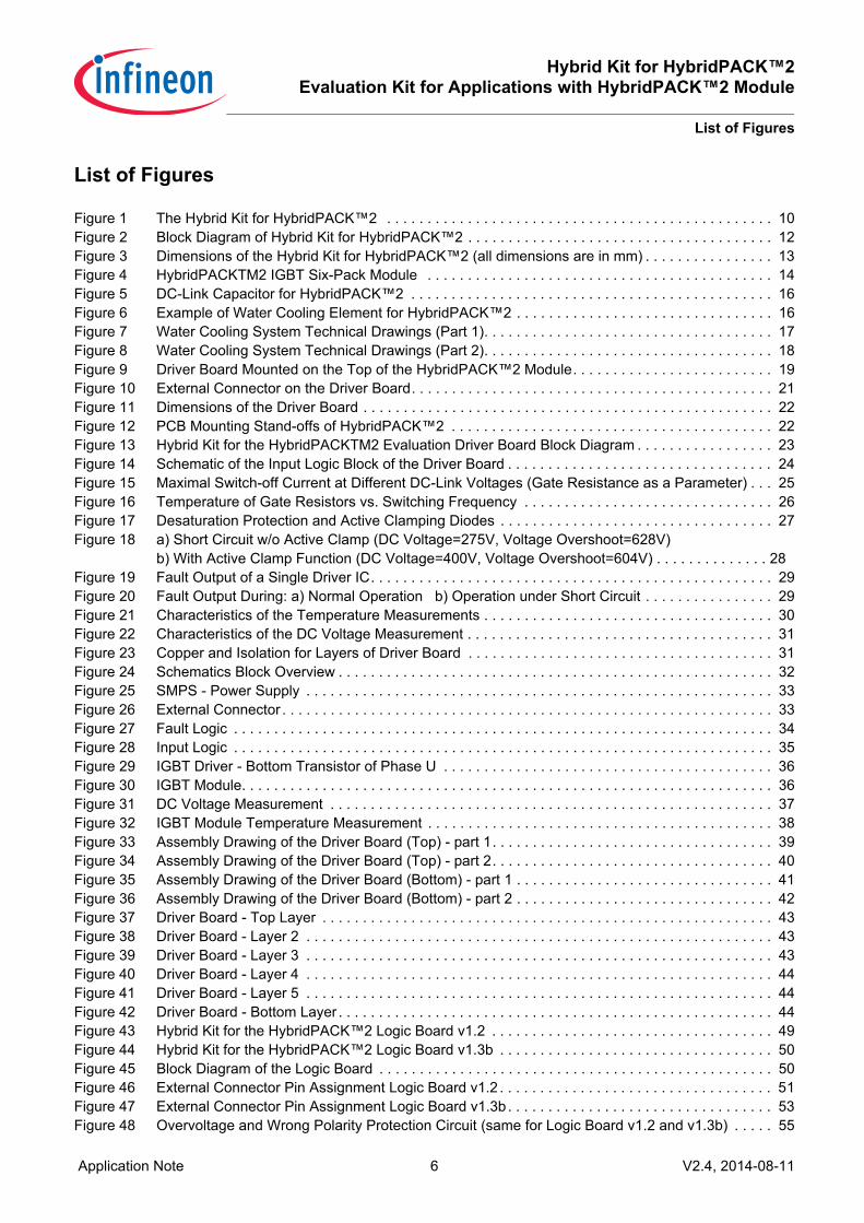
Figure 1 The Hybrid Kit for HybridPACK™2 . . . . . . . . . . . . . . . . . . . . . . . . . . . . . . . . . . . . . . . . . . . . . . . . 10Figure 2 Block Diagram of Hybrid Kit for HybridPACK™2 . . . . . . . . . . . . . . . . . . . . . . . . . . . . . . . . . . . . . . 12Figure 3 Dimensions of the Hybrid Kit for HybridPACK™2 (all dimensions are in mm) . . . . . . . . . . . . . . . . 13Figure 4 HybridPACKTM2 IGBT Six-Pack Module . . . . . . . . . . . . . . . . . . . . . . . . . . . . . . . . . . . . . . . . . . . 14Figure 5 DC-Link Capacitor for HybridPACK™2 . . . . . . . . . . . . . . . . . . . . . . . . . . . . . . . . . . . . . . . . . . . . . 16Figure 6 Example of Water Cooling Element for HybridPACK™2 . . . . . . . . . . . . . . . . . . . . . . . . . . . . . . . . 16Figure 7 Water Cooling System Technical Drawings (Part 1). . . . . . . . . . . . . . . . . . . . . . . . . . . . . . . . . . . . 17Figure 8 Water Cooling System Technical Drawings (Part 2). . . . . . . . . . . . . . . . . . . . . . . . . . . . . . . . . . . . 18Figure 9 Driver Board Mounted on the Top of the HybridPACK™2 Module. . . . . . . . . . . . . . . . . . . . . . . . . 19Figure 10 External Connector on the Driver Board. . . . . . . . . . . . . . . . . . . . . . . . . . . . . . . . . . . . . . . . . . . . . 21Figure 11 Dimensions of the Driver Board . . . . . . . . . . . . . . . . . . . . . . . . . . . . . . . . . . . . . . . . . . . . . . . . . . . 22Figure 12 PCB Mounting Stand-offs of HybridPACK™2 . . . . . . . . . . . . . . . . . . . . . . . . . . . . . . . . . . . . . . . . 22Figure 13 Hybrid Kit for the HybridPACKTM2 Evaluation Driver Board Block Diagram . . . . . . . . . . . . . . . . . 23Figure 14 Schematic of the Input Logic Block of the Driver Board . . . . . . . . . . . . . . . . . . . . . . . . . . . . . . . . . 24Figure 15 Maximal Switch-off Current at Different DC-Link Voltages (Gate Resistance as a Parameter) . . . 25Figure 16 Temperature of Gate Resistors vs. Switching Frequency . . . . . . . . . . . . . . . . . . . . . . . . . . . . . . . 26Figure 17 Desaturation Protection and Active Clamping Diodes . . . . . . . . . . . . . . . . . . . . . . . . . . . . . . . . . . 27Figure 18 a) Short Circuit w/o Active Clamp (DC Voltage=275V, Voltage Overshoot=628V)
b) With Active Clamp Function (DC Voltage=400V, Voltage Overshoot=604V) . . . . . . . . . . . . . . 28Figure 19 Fault Output of a Single Driver IC. . . . . . . . . . . . . . . . . . . . . . . . . . . . . . . . . . . . . . . . . . . . . . . . . . 29Figure 20 Fault Output During: a) Normal Operation b) Operation under Short Circuit . . . . . . . . . . . . . . . . 29Figure 21 Characteristics of the Temperature Measurements . . . . . . . . . . . . . . . . . . . . . . . . . . . . . . . . . . . . 30Figure 22 Characteristics of the DC Voltage Measurement . . . . . . . . . . . . . . . . . . . . . . . . . . . . . . . . . . . . . . 31Figure 23 Copper and Isolation for Layers of Driver Board . . . . . . . . . . . . . . . . . . . . . . . . . . . . . . . . . . . . . . 31Figure 24 Schematics Block Overview . . . . . . . . . . . . . . . . . . . . . . . . . . . . . . . . . . . . . . . . . . . . . . . . . . . . . . 32Figure 25 SMPS - Power Supply . . . . . . . . . . . . . . . . . . . . . . . . . . . . . . . . . . . . . . . . . . . . . . . . . . . . . . . . . . 33Figure 26 External Connector . . . . . . . . . . . . . . . . . . . . . . . . . . . . . . . . . . . . . . . . . . . . . . . . . . . . . . . . . . . . . 33Figure 27 Fault Logic . . . . . . . . . . . . . . . . . . . . . . . . . . . . . . . . . . . . . . . . . . . . . . . . . . . . . . . . . . . . . . . . . . . 34Figure 28 Input Logic . . . . . . . . . . . . . . . . . . . . . . . . . . . . . . . . . . . . . . . . . . . . . . . . . . . . . . . . . . . . . . . . . . . 35Figure 29 IGBT Driver - Bottom Transistor of Phase U . . . . . . . . . . . . . . . . . . . . . . . . . . . . . . . . . . . . . . . . . 36Figure 30 IGBT Module. . . . . . . . . . . . . . . . . . . . . . . . . . . . . . . . . . . . . . . . . . . . . . . . . . . . . . . . . . . . . . . . . . 36Figure 31 DC Voltage Measurement . . . . . . . . . . . . . . . . . . . . . . . . . . . . . . . . . . . . . . . . . . . . . . . . . . . . . . . 37Figure 32 IGBT Module Temperature Measurement . . . . . . . . . . . . . . . . . . . . . . . . . . . . . . . . . . . . . . . . . . . 38Figure 33 Assembly Drawing of the Driver Board (Top) - part 1. . . . . . . . . . . . . . . . . . . . . . . . . . . . . . . . . . . 39Figure 34 Assembly Drawing of the Driver Board (Top) - part 2. . . . . . . . . . . . . . . . . . . . . . . . . . . . . . . . . . . 40Figure 35 Assembly Drawing of the Driver Board (Bottom) - part 1 . . . . . . . . . . . . . . . . . . . . . . . . . . . . . . . . 41Figure 36 Assembly Drawing of the Driver Board (Bottom) - part 2 . . . . . . . . . . . . . . . . . . . . . . . . . . . . . . . . 42Figure 37 Driver Board - Top Layer . . . . . . . . . . . . . . . . . . . . . . . . . . . . . . . . . . . . . . . . . . . . . . . . . . . . . . . . 43Figure 38 Driver Board - Layer 2 . . . . . . . . . . . . . . . . . . . . . . . . . . . . . . . . . . . . . . . . . . . . . . . . . . . . . . . . . . 43Figure 39 Driver Board - Layer 3 . . . . . . . . . . . . . . . . . . . . . . . . . . . . . . . . . . . . . . . . . . . . . . . . . . . . . . . . . . 43Figure 40 Driver Board - Layer 4 . . . . . . . . . . . . . . . . . . . . . . . . . . . . . . . . . . . . . . . . . . . . . . . . . . . . . . . . . . 44Figure 41 Driver Board - Layer 5 . . . . . . . . . . . . . . . . . . . . . . . . . . . . . . . . . . . . . . . . . . . . . . . . . . . . . . . . . . 44Figure 42 Driver Board - Bottom Layer . . . . . . . . . . . . . . . . . . . . . . . . . . . . . . . . . . . . . . . . . . . . . . . . . . . . . . 44Figure 43 Hybrid Kit for the HybridPACK™2 Logic Board v1.2 . . . . . . . . . . . . . . . . . . . . . . . . . . . . . . . . . . . 49Figure 44 Hybrid Kit for the HybridPACK™2 Logic Board v1.3b . . . . . . . . . . . . . . . . . . . . . . . . . . . . . . . . . . 50Figure 45 Block Diagram of the Logic Board . . . . . . . . . . . . . . . . . . . . . . . . . . . . . . . . . . . . . . . . . . . . . . . . . 50Figure 46 External Connector Pin Assignment Logic Board v1.2 . . . . . . . . . . . . . . . . . . . . . . . . . . . . . . . . . . 51Figure 47 External Connector Pin Assignment Logic Board v1.3b . . . . . . . . . . . . . . . . . . . . . . . . . . . . . . . . . 53Figure 48 Overvoltage and Wrong Polarity Protection Circuit (same for Logic Board v1.2 and v1.3b) . . . . . 55
List of Figures

Hybrid Kit for HybridPACK™2Evaluation Kit for Applications with HybridPACK™2 Module
List of Figures
Application Note 7 V2.4, 2014-08-11
Figure 49 HW Boot Configuration of TC1767 DIP-Switch . . . . . . . . . . . . . . . . . . . . . . . . . . . . . . . . . . . . . . . 56Figure 50 The Boot Configuration Switch (SW1) and Serial/Parallel Interface Select Switch (SW2) . . . . . . . 57Figure 51 GMR SSC Interface (Logic Board v1.3b only) . . . . . . . . . . . . . . . . . . . . . . . . . . . . . . . . . . . . . . . . 59Figure 52 GMR SSC Interface - Proposal Using TLE5012. . . . . . . . . . . . . . . . . . . . . . . . . . . . . . . . . . . . . . . 60Figure 53 Picture of Possible Physical Implementation of the GMR Sensor . . . . . . . . . . . . . . . . . . . . . . . . . 60Figure 54 Definition of the Layers for the Logic Board v1.2 . . . . . . . . . . . . . . . . . . . . . . . . . . . . . . . . . . . . . . 61Figure 55 Definition of the Layers for the Logic Board v1.3b . . . . . . . . . . . . . . . . . . . . . . . . . . . . . . . . . . . . . 61Figure 56 Schematics Block Overview Logic Board v1.2 . . . . . . . . . . . . . . . . . . . . . . . . . . . . . . . . . . . . . . . . 62Figure 57 Schematics Block Overview Logic Board v1.3b . . . . . . . . . . . . . . . . . . . . . . . . . . . . . . . . . . . . . . . 63Figure 58 Power Supply Logic Board v1.2 . . . . . . . . . . . . . . . . . . . . . . . . . . . . . . . . . . . . . . . . . . . . . . . . . . . 64Figure 59 Power Supply Logic Board v1.3b . . . . . . . . . . . . . . . . . . . . . . . . . . . . . . . . . . . . . . . . . . . . . . . . . . 65Figure 60 JTAG Debug Connector (same for Logic Board v1.2 and v1.3b) . . . . . . . . . . . . . . . . . . . . . . . . . . 65Figure 61 Watchdog (same for Logic Board v1.2 and v1.3b) . . . . . . . . . . . . . . . . . . . . . . . . . . . . . . . . . . . . . 66Figure 62 Resolver Logic Board v1.2 . . . . . . . . . . . . . . . . . . . . . . . . . . . . . . . . . . . . . . . . . . . . . . . . . . . . . . . 66Figure 63 Resolver Logic Board v1.3b . . . . . . . . . . . . . . . . . . . . . . . . . . . . . . . . . . . . . . . . . . . . . . . . . . . . . . 67Figure 64 Level Shifter for Adapting 3.3V to 5V Logic Levels Logic Board v1.2. . . . . . . . . . . . . . . . . . . . . . . 67Figure 65 Level Shifter for Adapting 3.3V to 5V Logic Levels Logic Board v1.3b. . . . . . . . . . . . . . . . . . . . . . 68Figure 66 Connector to the Driver Board (same for Logic Board v1.2 and v1.3b) . . . . . . . . . . . . . . . . . . . . . 68Figure 67 Microcontroller Logic Board v1.2 . . . . . . . . . . . . . . . . . . . . . . . . . . . . . . . . . . . . . . . . . . . . . . . . . . 69Figure 68 Microcontroller Logic Board v1.3b . . . . . . . . . . . . . . . . . . . . . . . . . . . . . . . . . . . . . . . . . . . . . . . . . 70Figure 69 Input Filter Logic Board v1.2. . . . . . . . . . . . . . . . . . . . . . . . . . . . . . . . . . . . . . . . . . . . . . . . . . . . . . 71Figure 70 Input Filter Logic Board v1.3b. . . . . . . . . . . . . . . . . . . . . . . . . . . . . . . . . . . . . . . . . . . . . . . . . . . . . 72Figure 71 Microcontroller TC1767 Pin Assignment Logic Board v1.2 . . . . . . . . . . . . . . . . . . . . . . . . . . . . . . 73Figure 72 Microcontroller TC1767 Pin Assignment Logic Board v1.3b . . . . . . . . . . . . . . . . . . . . . . . . . . . . . 74Figure 73 EEPROM (same for Logic Board v1.2 and Logic Board v1.3b) . . . . . . . . . . . . . . . . . . . . . . . . . . . 75Figure 74 On-Board Temperature Measurement (Logic Board v1.3b only) . . . . . . . . . . . . . . . . . . . . . . . . . . 75Figure 75 Assembly Drawing of the Logic Board v1.2 (Top) . . . . . . . . . . . . . . . . . . . . . . . . . . . . . . . . . . . . . 76Figure 76 Assembly Drawing of the Logic Board v1.3b (Top) . . . . . . . . . . . . . . . . . . . . . . . . . . . . . . . . . . . . 77Figure 77 Assembly Drawing of the Logic Board v1.2 (Bottom) . . . . . . . . . . . . . . . . . . . . . . . . . . . . . . . . . . . 78Figure 78 Assembly Drawing of the Logic Board v1.3b (Bottom) . . . . . . . . . . . . . . . . . . . . . . . . . . . . . . . . . . 79Figure 79 Logic Board v1.2 - Top Layer . . . . . . . . . . . . . . . . . . . . . . . . . . . . . . . . . . . . . . . . . . . . . . . . . . . . . 80Figure 80 Logic Board v1.2 - Layer 2 . . . . . . . . . . . . . . . . . . . . . . . . . . . . . . . . . . . . . . . . . . . . . . . . . . . . . . . 81Figure 81 Logic Board v1.2 - Layer 3 . . . . . . . . . . . . . . . . . . . . . . . . . . . . . . . . . . . . . . . . . . . . . . . . . . . . . . . 82Figure 82 Logic Board v1.2 - Bottom Layer . . . . . . . . . . . . . . . . . . . . . . . . . . . . . . . . . . . . . . . . . . . . . . . . . . 83Figure 83 Logic Board v1.3b - Top Layer . . . . . . . . . . . . . . . . . . . . . . . . . . . . . . . . . . . . . . . . . . . . . . . . . . . . 84Figure 84 Logic Board v1.3b - Layer 2 . . . . . . . . . . . . . . . . . . . . . . . . . . . . . . . . . . . . . . . . . . . . . . . . . . . . . . 85Figure 85 Logic Board v1.3b - Layer 3 . . . . . . . . . . . . . . . . . . . . . . . . . . . . . . . . . . . . . . . . . . . . . . . . . . . . . . 86Figure 86 Logic Board v1.3b - Layer 4 . . . . . . . . . . . . . . . . . . . . . . . . . . . . . . . . . . . . . . . . . . . . . . . . . . . . . . 87Figure 87 Logic Board v1.3b - Layer 5 . . . . . . . . . . . . . . . . . . . . . . . . . . . . . . . . . . . . . . . . . . . . . . . . . . . . . . 88Figure 88 Logic Board v1.3b - Bottom Layer . . . . . . . . . . . . . . . . . . . . . . . . . . . . . . . . . . . . . . . . . . . . . . . . . 89

Hybrid Kit for HybridPACK™2Evaluation Kit for Applications with HybridPACK™2 Module
List of Tables
Application Note 8 V2.4, 2014-08-11
Table 1 Key Data of DC-Link Capacitor . . . . . . . . . . . . . . . . . . . . . . . . . . . . . . . . . . . . . . . . . . . . . . . . . . . 15Table 2 Key Data and Characteristic Values (Typical Values) . . . . . . . . . . . . . . . . . . . . . . . . . . . . . . . . . . 20Table 3 Bill of Materials for Hybrid Kit for the HybridPACK™2 Evaluation Driver Board . . . . . . . . . . . . . . 45Table 4 External Connection Pin Assignment Logic Board v1.2 . . . . . . . . . . . . . . . . . . . . . . . . . . . . . . . . . 51Table 5 External Connector Pin Assignment Logic Board v1.3b . . . . . . . . . . . . . . . . . . . . . . . . . . . . . . . . . 54Table 6 User Startup Modes for TC1767 . . . . . . . . . . . . . . . . . . . . . . . . . . . . . . . . . . . . . . . . . . . . . . . . . . 57Table 7 Selecting Serial/Parallel Interface . . . . . . . . . . . . . . . . . . . . . . . . . . . . . . . . . . . . . . . . . . . . . . . . . 57Table 8 Bill of Materials for Hybrid Kit for the HybridPACK™2 Logic Board v1.2 . . . . . . . . . . . . . . . . . . . . 90Table 9 Bill of Materials for hybrid Kit for HybridPACK™2 Logic Board v1.3b . . . . . . . . . . . . . . . . . . . . . . 92
List of Tables

Hybrid Kit for HybridPACK™2Evaluation Kit for Applications with HybridPACK™2 Module
List of Tables
Application Note 9 V2.4, 2014-08-11

Hybrid Kit for HybridPACK™2Evaluation Kit for Applications with HybridPACK™2 Module
Introduction
Application Note 10 V2.4, 2014-08-11
1 IntroductionThe Hybrid Kit for HybridPACK™2 shown in Figure 1 was developed to support customers during their firststeps in designing applications with HybridPACK™2 IGBT module. The following chapters provide a detaileddescription of the main components and their functionality. This information is intended to enable the customersto re-use and modify the original Hybrid Kit design and qualify their own design for the production, according totheir own specific requirements. The boards Hybrid Kit for HybridPACKTM2 Evaluation Driver Board (further referred as “Driver Board” ) andHybrid Kit for HybridPACKTM2 Logic Board (further referred as “Logic Board”) provided by InfineonTechnologies are subjected to functional testing only. The current implementation of the Hybrid Kit for HybridPACKTM2 (e.g. electrical schematics) is for referenceonly! It does not cover in general all application specific requirements. For specific recommendations on howto implement designs with HybridPACKTM2 and EiceDRIVER™, please contact your local Infineon sales partner.More information is available on www.infineon.com.Due to their purpose the system is not subjected to the same procedures regarding Returned Material Analysis(RMA), Process Change Notification (PCN) and Product Withdraw (PWD) as regular products.See Legal Disclaimer and Warnings for further restrictions on Infineon Technologies’ warranty and liability.
1.1 How to Order Hybrid Kit for HybridPACK™2Hybrid Kit for HybridPACK™2 and Hybrid Kit for HybridPACK™2 Evaluation Driver Board (that can beordered separately) have Infineon Technologies SAP numbers and can be ordered via Infineon Sales Partners.• SAP ordering number for Hybrid Kit for HybridPACK™2: SP000635950 • SAP ordering number for Hybrid Kit for HybridPACK™2 Evaluation Driver Board: SP000552868Information can also be found at the Infineon Technologies web page: www.infineon.com
Figure 1 The Hybrid Kit for HybridPACK™2

Hybrid Kit for HybridPACK™2Evaluation Kit for Applications with HybridPACK™2 Module
Introduction
Application Note 11 V2.4, 2014-08-11
W A R N I N G !Please always take care of the dead-time settings of the driver (toavoid short circuit conditions on the IGBT module) and alwayshave on mind that Hybrid Kit for HybridPACKTM2 inverter has nobreaking chopper or similar hardware protection to absorb theenergy generated during the regenerative breaking of a motor. Inany case user shall ensure that voltage, current and temperatureare monitored properly, e.g. by software or additional supportinghardware.

Hybrid Kit for HybridPACK™2Evaluation Kit for Applications with HybridPACK™2 Module
Design Features
Application Note 12 V2.4, 2014-08-11
2 Design FeaturesThe Hybrid Kit for HybridPACK™2 is made up of two PCBs (Driver Board and Logic Board) mechanically andelectrically suitable to be used with an IGBT Module HybridPACK™2 (included), a DC-bus capacitor and a cooler.All these components build a complete main inverter for (H)EV applications up to 80kW.
Figure 2 Block Diagram of Hybrid Kit for HybridPACK™2
Figure 2 show the complete block diagram for the system and the following sections provide an overview of thesingle components including main features, key data, pin assignments and mechanical dimensions.
2.1 Main Features• Complete main inverter for (H)EV applications up to 80kW • Automotive qualified IGBT module HybridPACK™2
– 650V/800A IGBT & Diode chipset• Automotive qualified Driver IC 1ED020I12-FA
– Based on coreless transformer technology– Up to 1200V and 2A driving capability– VCE sat - detection
• TriCore™ family 32-bit microcontroller TC1767: member of the AUDO FUTURE product family designed for automotive applications
• Possibility of usage of different motor position interfaces: encoder, resolver, GMR (Giant Magneto-Resistance) or hall sensor
IGBT Module HybridPACK™2
6ED100HP1-FA Driver Board
IGBT driver 1ED020I12-FA
SMPS
Logic
IGBT Temp. Measurement
DC-Bus Voltage Measurement
(Isolated)
PWM
Temp. IGBT (x3)FAULTSignals
RST
VDC meas.
Logic Board
Supply
Connector
Supply
Debug Connector
MicrocontrollerTC1767
Resolver InterfaceI, U, V Current
MeasurementResolver
A/D IO
CAN / RS232
Encoder
EEPROM
Supply
Watchdog
LevelShifter
VDC, Temp
Other Sensor
IGBT driver 1ED020I12-FA
IGBT driver 1ED020I12-FA
IGBT driver 1ED020I12-FA
IGBT driver 1ED020I12-FA
IGBT driver 1ED020I12-FA
ResolverEncoder
RS232CAN
Current W
Current V
Current U
Co
nn
ec
to
r
Co
nn
ec
to
r
Other Sensor

Hybrid Kit for HybridPACK™2Evaluation Kit for Applications with HybridPACK™2 Module
Design Features
Application Note 13 V2.4, 2014-08-11
2.2 DimensionsFigure 3 shows the dimensions of a complete Hybrid Kit for HybridPACK™2.
Figure 3 Dimensions of the Hybrid Kit for HybridPACK™2 (all dimensions are in mm)
Remark: Logic Board v1.3b is 2mm longer than Logic Board v1.2 (100.4 mm comparing to 98.4 mm).
2.3 Key ComponentsFor detailed technical information about the different components please refer to the different web pages on theInfineon Internet.
2.3.1 Driver Board (6ED100HP2-FA)The 6ED100HP2-FA is a six channel IGBT driver board, specially designed for the HybridPACK™2 IGBT module.The main features and a detailed description of the board, including schematics and layout, can be found inChapter 3.
237.0
98.4
216.0
50.0
25.0 41.5
75.5
65.0 47.4

Hybrid Kit for HybridPACK™2Evaluation Kit for Applications with HybridPACK™2 Module
Design Features
Application Note 14 V2.4, 2014-08-11
2.3.2 Logic BoardThe Logic Board contains all necessary components for the control of the system. Furthermore it offers theconnections to the motor positioning system (encoder, resolver or GMR) and to the current measurement system.For a detailed description of the board please refer to Chapter 3.
2.3.3 HybridPACK™2 (see Figure 4) is a power module designed for Full Hybrid Electrical Vehicle (HEV) applications for a power rangeup to 80kW. Designed for a junction operation temperature at 150°C, the module accommodates a six-packconfiguration of 3rd generation Trench-Field-Stop IGBT and matching emitter controlled diodes and is rated up to800A/650V. It is based on Infineon Technologies leading TRENCHSTOPTM IGBT Technology, which offers lowestconduction and switching losses.
HybridPACK™2 is designed for direct water-cooled inverter systems (temperature of coolant 75°C). The Pin Fincopper base plate combined with high-performance ceramic substrate and Infineon Technologies enhanced wire-bonding process provides unparalleled thermal cycling and power cycling reliability for full hybrid inverterapplications. For a compact inverter design the driver stage PCB can easily be soldered on top of the module. Allpower connections are realized with screw terminals.
Figure 4 HybridPACKTM2 IGBT Six-Pack Module

Hybrid Kit for HybridPACK™2Evaluation Kit for Applications with HybridPACK™2 Module
Design Features
Application Note 15 V2.4, 2014-08-11
2.3.4 DC-Link CapacitorsFor Hybrid Kit for HybridPACK™2 are used Epcos B25655J4507K and Kemet C4EEGMX6500AAUK as DC buscapacitors.
2.3.4.1 EPCOS B25655J4507KThe main features of the power electronic capacitor B25655J4507K from Epcos AG (see Figure 5) are shown inTable 1. Please refer to the Epcos datasheet for further details.
Table 1 Key Data of DC-Link CapacitorCharacteristics Maximum ratings Test DataCR 500 µF ±10% Vs 600V VTT 675V DC, 10sVR 450V DC î 2kA Rins ·C ≥ 10000sWR 50Ws Is 8kA tan δ (50 Hz) ≤ 8 · 10-4
Imax 120A (dV/dt)max 4V/µsLself 15nH (dV/dt)s 16V/µstan δ0 2 · 10-4
Rs 1.0mΩ
Climatic Category 0/110/21(IEC 68-1/2)
Design Data
Tmin - 40°C Dimensions l × w × h 237 × 72 × 50 mmTmax + 110°C Approx. weight 1.2kgMax. Rel. Humidity ≤ 95% Impregnation Resin FilledTstg - 45 … +110°C Terminals Flat Copper
Clearance 8 mmValues after Test Ca, IEC 68-2 (21 days, 40°C, 93% rel. humidity)
Creepage distance 8mm
ΔC/C ≤ 5% Plastic CaseΔtanδ ≤ 4 ·10-4
Rins ·C ≥ 3000s
Mean Life ExpentancytLD 15000hαFQ 300fit

Hybrid Kit for HybridPACK™2Evaluation Kit for Applications with HybridPACK™2 Module
Design Features
Application Note 16 V2.4, 2014-08-11
Figure 5 DC-Link Capacitor for HybridPACK™2 B25655J4507K from EPCOS AG

Hybrid Kit for HybridPACK™2Evaluation Kit for Applications with HybridPACK™2 Module
Design Features
Application Note 17 V2.4, 2014-08-11
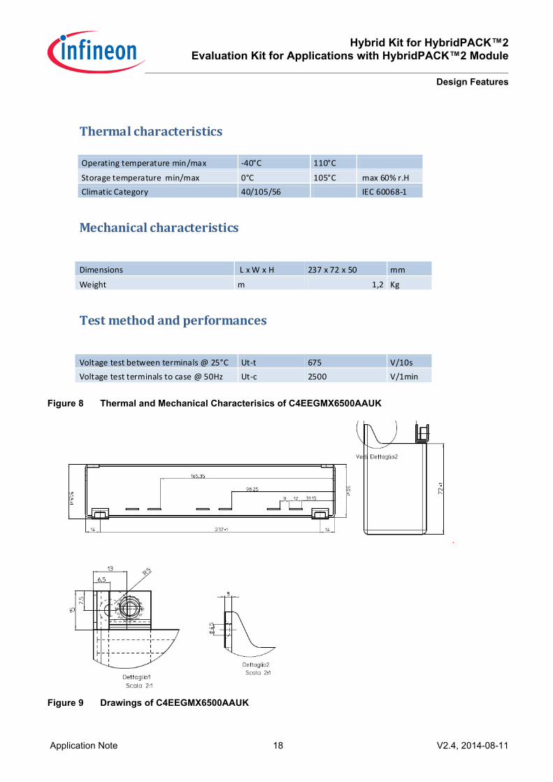
2.3.4.2 Kemet C4EEGMX6500AAUKThe power electronic capacitor C4EEGMX6500AAUK (see Figure 6) from KEMET Electronics is a metallizedseal-healing polypropylene capacitor with a non-inductive winding. The plastic case is filled with resin for longtermhumidity protection. Two battery connections and 6 terminals 6mm holes for the connection to the IGBTs.Electrical perfomance is given on Figure 7, thermal and mechanical characteristics are given in Figure 8 anddrawings are shown in Figure 9.
Figure 6 DC-Link Capacitor for HybridPACK™2 C4EEGMX6500AAUK from KEMET Electronics
Figure 7 Electrical performance of C4EEGMX6500AAUK
Nominal capacitance C_nom 500 µF @RT ± 5°C Tolerance C_tol ± 10 %
Rated DC voltage U_rated 450 VDC @105°C Peak voltage U_peak 650 VDC for 10sec
Nominal RMS current I_max_rms 120 A @10kHz; T_case <105°C Max peak current I_peak 2500 A @450VDC;dv/dt = 2V/µs
Equivalent Series resistance ESR 1 mOhm @ 1kHz Equivalent Series inductance ESL 15 nH
Dissipation factor@1kHz DF 0,01 % @1 kHz Max pulse rise time (dv/dt)max 5 V/µs
Min Insulation resistance Ris 20 MOhm 500VDC; for120sec
Lifetime Lexp 15000 hours T_hotspot_max >=90°C FIT FIT 300 1/kpcsHours
Hybrid Kit for HybridPACK™2Evaluation Kit for Applications with HybridPACK™2 Module
Design Features
Application Note 18 V2.4, 2014-08-11
Figure 8 Thermal and Mechanical Characterisics of C4EEGMX6500AAUK
Figure 9 Drawings of C4EEGMX6500AAUK
Thermal characteristics Operating temperature min/max -40°C 110°C
Storage temperature min/max 0°C 105°C max 60% r.H Climatic Category 40/105/56 IEC 60068-1
Mechanical characteristics
Dimensions L x W x H 237 x 72 x 50 mm
Weight m 1,2 Kg
Test method and performances
Voltage test between terminals @ 25°C Ut-t 675 V/10s Voltage test terminals to case @ 50Hz Ut-c 2500 V/1min

Hybrid Kit for HybridPACK™2Evaluation Kit for Applications with HybridPACK™2 Module
Design Features
Application Note 19 V2.4, 2014-08-11
2.3.5 Cooling ElementFor applications requiring higher power or higher operation temperature a usage of water cooling element isrecommended. Figure 10 shows the low cost water cooling system that is included in the Hybrid Kit forHybridPACK™2 which can be screwed directly to HybridPACK™2 - Figure 11 and Figure 12 are showing thetechnical drawings of it.
Figure 10 Example of Water Cooling Element for HybridPACK™2

Hybrid Kit for HybridPACK™2Evaluation Kit for Applications with HybridPACK™2 Module
Design Features
Application Note 20 V2.4, 2014-08-11
Figure 11 Water Cooling System Technical Drawings (Part 1)

Hybrid Kit for HybridPACK™2Evaluation Kit for Applications with HybridPACK™2 Module
Design Features
Application Note 21 V2.4, 2014-08-11
Figure 12 Water Cooling System Technical Drawings (Part 2)

Hybrid Kit for HybridPACK™2Evaluation Kit for Applications with HybridPACK™2 Module
Hybrid Kit for the HybridPACK™2 Evaluation Driver Board
Application Note 22 V2.4, 2014-08-11
3 Hybrid Kit for the HybridPACK™2 Evaluation Driver Board
Figure 13 Driver Board Mounted on the Top of the HybridPACK™2 Module
3.1 Main FeaturesThe Hybrid Kit for HybridPACK™2 Evaluation Driver Board offers the following features:• Six channel IGBT driver • Electrically and mechanically suitable for 650 V IGBT Module HybridPACK™2• Includes DC/DC power supply • Isolated voltage measurement• Short circuit protection with toff < 6 µs• Undervoltage lockout of IGBT driver IC• Positive logic with 5 V CMOS level for PWM and Fault signals• One fault output signal for each leg and one common for all legsImportant: - if a Driver Board is used as a standalone board (without Logic Board from Hybrid Kit), the resistorR534 (please refer to Figure 29) should be populated (0R) to connect 2 grounds (“digital” and “analog”). If thesetwo grounds are not connected one can notice some signal disturbances. If the Driver Board is used together withthe Logic Board (as in a complete Hybrid Kit) the 2 grounds are already connected on the Logic Board (thereforeit is in design of Driver Board the R534 unpopulated) and no modification (soldering) should be taken on a DriverBoard.
Hybrid Kit for HybridPACK™2Evaluation Kit for Applications with HybridPACK™2 Module
Hybrid Kit for the HybridPACK™2 Evaluation Driver Board
Application Note 23 V2.4, 2014-08-11
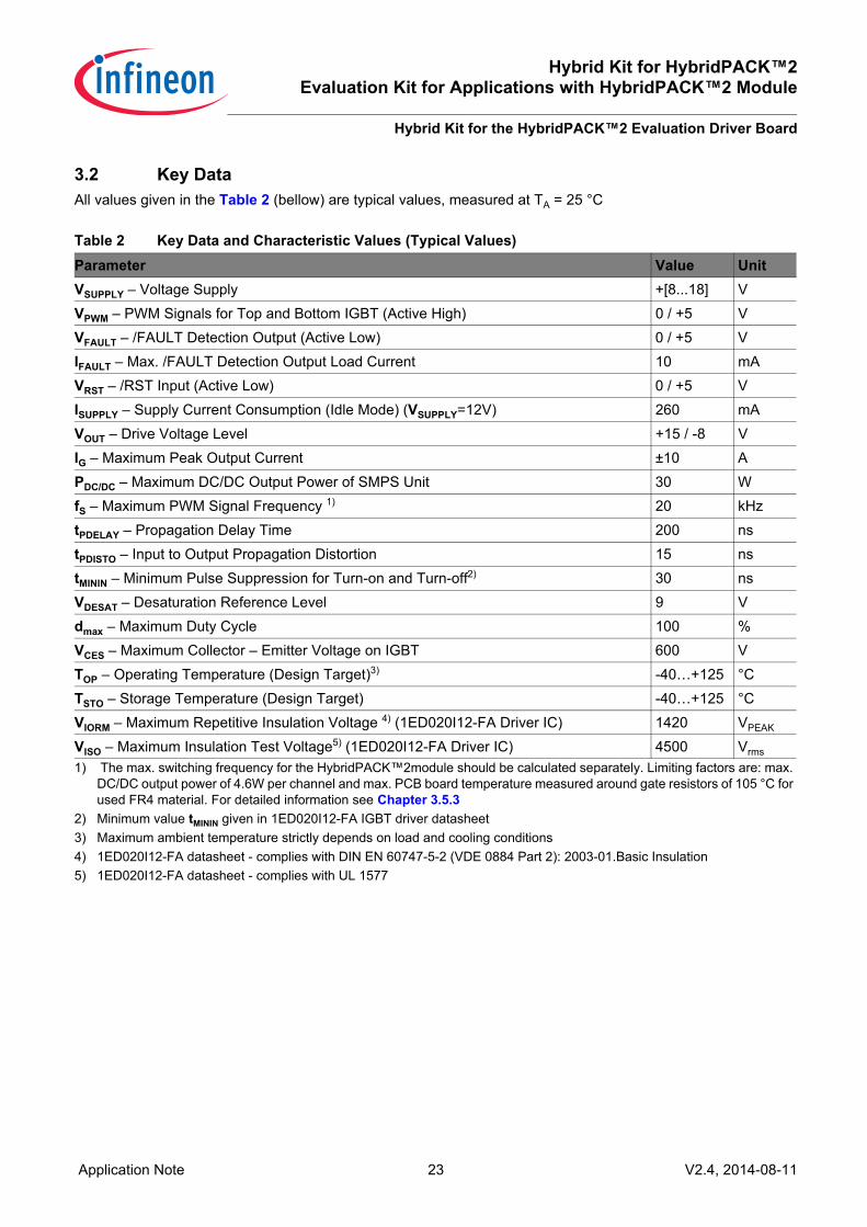
3.2 Key DataAll values given in the Table 2 (bellow) are typical values, measured at TA = 25 °C
Table 2 Key Data and Characteristic Values (Typical Values)Parameter Value UnitVSUPPLY – Voltage Supply +[8...18] VVPWM – PWM Signals for Top and Bottom IGBT (Active High) 0 / +5 VVFAULT – /FAULT Detection Output (Active Low) 0 / +5 VIFAULT – Max. /FAULT Detection Output Load Current 10 mAVRST – /RST Input (Active Low) 0 / +5 VISUPPLY – Supply Current Consumption (Idle Mode) (VSUPPLY=12V) 260 mAVOUT – Drive Voltage Level +15 / -8 VIG – Maximum Peak Output Current ±10 APDC/DC – Maximum DC/DC Output Power of SMPS Unit 30 WfS – Maximum PWM Signal Frequency 1)
1) The max. switching frequency for the HybridPACK™2module should be calculated separately. Limiting factors are: max. DC/DC output power of 4.6W per channel and max. PCB board temperature measured around gate resistors of 105 °C for used FR4 material. For detailed information see Chapter 3.5.3
20 kHztPDELAY – Propagation Delay Time 200 nstPDISTO – Input to Output Propagation Distortion 15 nstMININ – Minimum Pulse Suppression for Turn-on and Turn-off2)
2) Minimum value tMININ given in 1ED020I12-FA IGBT driver datasheet
30 nsVDESAT – Desaturation Reference Level 9 Vdmax – Maximum Duty Cycle 100 %VCES – Maximum Collector – Emitter Voltage on IGBT 600 VTOP – Operating Temperature (Design Target)3)
3) Maximum ambient temperature strictly depends on load and cooling conditions
-40…+125 °CTSTO – Storage Temperature (Design Target) -40…+125 °CVIORM – Maximum Repetitive Insulation Voltage 4) (1ED020I12-FA Driver IC)
4) 1ED020I12-FA datasheet - complies with DIN EN 60747-5-2 (VDE 0884 Part 2): 2003-01.Basic Insulation
1420 VPEAK
VISO – Maximum Insulation Test Voltage5) (1ED020I12-FA Driver IC)
5) 1ED020I12-FA datasheet - complies with UL 1577
4500 Vrms
Hybrid Kit for HybridPACK™2Evaluation Kit for Applications with HybridPACK™2 Module
Hybrid Kit for the HybridPACK™2 Evaluation Driver Board
Application Note 24 V2.4, 2014-08-11
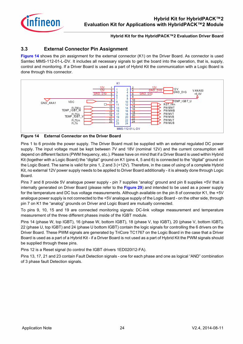
3.3 External Connector Pin AssignmentFigure 14 shows the pin assignment for the external connector (K1) on the Driver Board. As connector is usedSamtec MMS-112-01-L-DV. It includes all necessary signals to get the board into the operation, that is, supply,control and monitoring. If a Driver Board is used as a part of Hybrid Kit the communication with a Logic Board isdone through this connector.
Figure 14 External Connector on the Driver Board
Pins 1 to 6 provide the power supply. The Driver Board must be supplied with an external regulated DC powersupply. The input voltage must be kept between 7V and 18V (nominal 12V) and the current consumption willdepend on different factors (PWM frequency, etc.). Please have on mind that if a Driver Board is used within HybridKit (together with a Logic Board) the “digital” ground on K1 (pins 4, 5 and 6) is connected to the “digital” ground onthe Logic Board. The same is valid for pins 1, 2 and 3 (+12V). Therefore, in the case of using of a complete HybridKit, no external 12V power supply needs to be applied to Driver Board additionally - it is already done through LogicBoard.Pins 7 and 8 provide 5V analogue power supply - pin 7 supplies “analog” ground and pin 8 supplies +5V that isinternally generated on Driver Board (please refer to the Figure 29) and intended to be used as a power supplyfor the temperature and DC bus voltage measurements. Although available on the pin 8 of connector K1, the +5Vanalogue power supply is not connected to the +5V analogue supply of the Logic Board - on the other side, throughpin 7 on K1 the “analog” grounds on Driver and Logic Board are mutually connected.To pins 9, 10, 15 and 19 are connected monitoring signals: DC-link voltage measurement and temperaturemeasurement of the three different phases inside of the IGBT module.Pins 14 (phase W, top IGBT), 16 (phase W, bottom IGBT), 18 (phase V, top IGBT), 20 (phase V, bottom IGBT),22 (phase U, top IGBT) and 24 (phase U bottom IGBT) contain the logic signals for controlling the 6 drivers on theDriver Board. These PWM signals are generated by TriCore TC1767 on the Logic Board in the case that a DriverBoard is used as a part of a Hybrid Kit - if a Driver Board is not used as a part of Hybrid Kit the PWM signals shouldbe supplied through these pins.Pins 12 is a Reset signal (to control the IGBT drivers 1ED020I12-FA).Pins 13, 17, 21 and 23 contain Fault Detection signals - one for each phase and one as logical “AND” combinationof 3 phase fault Detection signals.
12V12V
12VGN D _D IG GN D _D IG
GN D _D I G
K1
MMS-112-01-L-D V
11 2 233 4 4
55 6 677 8 8
99 10 101111 12 12
1313 14 141515 16 16
1717 18 181919 20 20
2121 22 222323 24 24
R ST_I N n
FLTnFLTU n
FLTW nPW MWBPW MWT
PW MVB
PW MU BPW MU T
TEMP_I GB T_U
FLTVn PW MVT
VD C
TEMP_I GBT_W
TEMP _IGBT_V
V AN A50+5. 0V
GN D _AN A1
12 VGN D _D I G

Hybrid Kit for HybridPACK™2Evaluation Kit for Applications with HybridPACK™2 Module
Hybrid Kit for the HybridPACK™2 Evaluation Driver Board
Application Note 25 V2.4, 2014-08-11
3.4 Mechanical Dimensions of the Driver Board
Figure 15 Dimensions of the Driver Board
The Driver Boards should be fastened by self taping screws and soldered to the auxiliary connectors on top of theIGBT module. The contact joints (solder points) between PCB and module auxiliary contacts should bemechanically relieved in order to disburden the solder connection as far as possible. Relieve of the contact pointsis carried out by mounting the PCB directly onto the module at the ten mounting stand-offs (see Figure 16) usingself-tapping screws (thread forming with 2.5mm diameter) or similar assembly material. The screws should bemounted in the sequence showed in Figure 16.
Figure 16 PCB Mounting Stand-offs of HybridPACK™2
max. 16.5 mmmax. 19 mm
216 mm
70m

Hybrid Kit for HybridPACK™2Evaluation Kit for Applications with HybridPACK™2 Module
Hybrid Kit for the HybridPACK™2 Evaluation Driver Board
Application Note 26 V2.4, 2014-08-11
3.5 Operation of the Driver Board
Figure 17 shows the block structure of the Driver Board. The following chapter describes these blocks in detail.
Figure 17 Hybrid Kit for the HybridPACKTM2 Evaluation Driver Board Block Diagram
3.5.1 Switching Mode Power Supply (SMPS)The Driver Board has an integrated DC/DC converter which generates the required secondary isolatedunsymmetrical supply voltage of +15/-8V. Top and bottom driver voltages are independently generated by usingone unipolar input voltage of 12V. An additional supply voltage (5V) is generated and forwarded to the external connector (K1, pin 7 and 8), so if aDriver Board is used as a standalone board, it can be used to supply external components in the system (currentmeasurement, motor interface, etc.)For circuit details please refer to Figure 29.
3.5.2 Input LogicThe Driver Board is a dedicated system for a six-pack HybridPACK™2 IGBT configuration - therefore it isnecessary to use 6 separated PWM signals. The schematics on Figure 18 shows the input logic block with +5Vpositive logic. The block is made up of RC filters for each PWM signal in order to reduce noise. Additionally thesesignals are pulled-down in order to avoid unwanted switching-on of the drivers. Please have on mind that theHybrid Kit for HybridPack™2 does not provide dead time automatically (meaning that hardware alone provides nodead time) - it is up to the user to generate the PWM signals with the correct dead time (by means of software).
IGBT Driver
UT
IGBT Driver
UB
IGBT Driver
VT
IGBT Driver
VB
IGBT Driver WT
IGBT Driver WB
SMPS 15V/-8V
15V/-8V15V/-8V
15V/-8V (x3)
5V5V 5V 5V
5V 5V 5V
Connector
LOGIC FAULT UFAULT V
FAULT W
RESET
FAU
LT WFA
ULT V
FAU
LT UFA
ULT
RE
SE
T
INPUTLOGIC(PWM)
DC LINK VOLTAGE MEASUREMENT
IGBT MODULTEMP
(U,V,W)
IGBT MODUL TEMPERATURE (U,V,W)
12V
DC LINKVOLTAGE
MEASUREMENT

Hybrid Kit for HybridPACK™2Evaluation Kit for Applications with HybridPACK™2 Module
Hybrid Kit for the HybridPACK™2 Evaluation Driver Board
Application Note 27 V2.4, 2014-08-11
Figure 18 Schematic of the Input Logic Block of the Driver Board
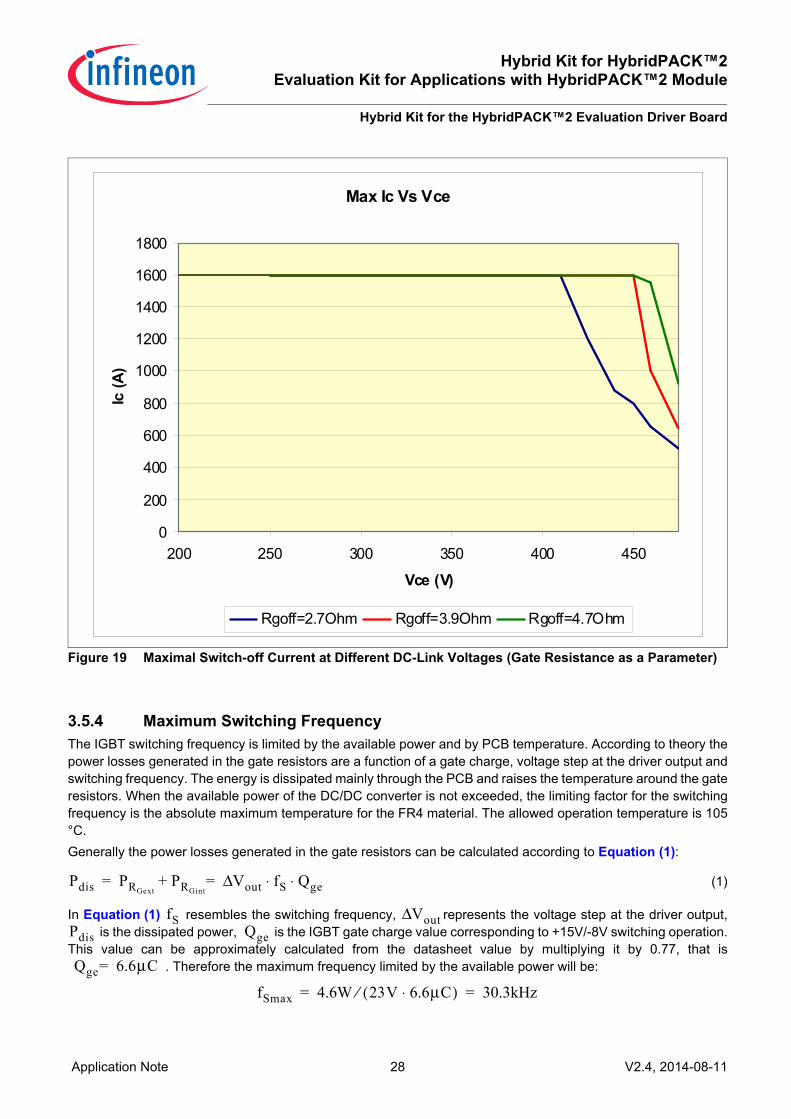
3.5.3 IGBT Switch-off BehaviorDue to the stray inductances of the system a voltage overshoots occur during the switching-off the IGBT. Suchovershoots are added to the DC-link voltage, so that the maximum blocking voltage of the IGBT or capacitor mightbe exceeded causing damages in both components (DC link capacitor and IGBT module). In order to avoid suchrisks an active clamping circuit is used (see Chapter 3.5.6).Without such protection methods the maximum current would be limited by the DC-link voltage and the voltageovershoots at switching-off. The voltage overshoots can be minimized by increasing the gate resistor, which willreduce the di/dt value. Figure 19 shows the maximal switch-off current at different DC-link voltages for a differentvalues of the gate resistor. These results were obtained with the DC-link capacitor described in Chapter 2.3.4.
C900100pF/100V/COG
R520100R
GND_DIG1
R52115k
GND_DIG1
C901100pF/100V/COG
R522100R
GND_DIG1
R52315k
GND_DIG1
C902100pF/100V/COG
R524100R
GND_DIG1
R52515k
GND_DIG1
C903100pF/100V/COG
R526100R
GND_DIG1
R52715k
GND_DIG1
C904100pF/100V/COG
R528100R
GND_DIG1
R52915k
GND_DIG1
C905100pF/100V/COG
R530100R
GND_DIG1
R53115k
GND_DIG1
PWM_WT
PWM_WB
PWM_VT
PWM_VB
PWM_UT
PWM_UB
PWMWT
PWMWB
PWMVT
PWMVB
PWMUT
PWMUB
Hybrid Kit for HybridPACK™2Evaluation Kit for Applications with HybridPACK™2 Module
Hybrid Kit for the HybridPACK™2 Evaluation Driver Board
Application Note 28 V2.4, 2014-08-11
Figure 19 Maximal Switch-off Current at Different DC-Link Voltages (Gate Resistance as a Parameter)
3.5.4 Maximum Switching Frequency The IGBT switching frequency is limited by the available power and by PCB temperature. According to theory thepower losses generated in the gate resistors are a function of a gate charge, voltage step at the driver output andswitching frequency. The energy is dissipated mainly through the PCB and raises the temperature around the gateresistors. When the available power of the DC/DC converter is not exceeded, the limiting factor for the switchingfrequency is the absolute maximum temperature for the FR4 material. The allowed operation temperature is 105°C. Generally the power losses generated in the gate resistors can be calculated according to Equation (1):
(1)
In Equation (1) resembles the switching frequency, represents the voltage step at the driver output, is the dissipated power, is the IGBT gate charge value corresponding to +15V/-8V switching operation.
This value can be approximately calculated from the datasheet value by multiplying it by 0.77, that is. Therefore the maximum frequency limited by the available power will be:
Max Ic Vs Vce
0
200
400
600
800
1000
1200
1400
1600
1800
200 250 300 350 400 450
Vce (V)
Ic (A
)
Rgoff=2.7Ohm Rgoff=3.9Ohm Rgoff=4.7Ohm
Pdis PRGextPRGint
Vout fS Qge⋅ ⋅Δ=+=
fS VoutΔPdis Qge
Qge 6.6μC=
fSmax 4.6W 23V 6.6μC⋅( )⁄ 30.3kHz= =

Hybrid Kit for HybridPACK™2Evaluation Kit for Applications with HybridPACK™2 Module
Hybrid Kit for the HybridPACK™2 Evaluation Driver Board
Application Note 29 V2.4, 2014-08-11
Figure 20 shows experimentally determined board temperature dependencies with switching frequency (at 26°Cambient temperature). From Figure 20 it can be concluded that the maximum switching frequency is limited byPCB temperature.
Figure 20 Temperature of Gate Resistors vs. Switching Frequency
3.5.5 BoosterTwo transistors per driver IC are used to amplify the driver ICs signals. On this way the driving IGBTs are suppliedwith sufficient current even if driver ICs alone can’t deliver enough current. One NPN transistor is used forswitching the IGBT on and another PNP transistor for switching the IGBT off.
The transistors are dimensioned to have enough peak current to drive HybridPACK™2 modules. Peak current canbe calculated like in Equation (2):
(2)
For circuit details please refer to Figure 33.
Gate resistor temperature Vs. switching frequency @ Ta=25°C
25
35
45
55
65
75
85
95
105
1 3 5 7 9 11 13 15 17 19
Switching frequency (KHz)
Gat
e re
sist
or te
mpe
ratu
re
IpeakVΔ out
RGintRGext
RDriver+ +-----------------------------------------------------=

Hybrid Kit for HybridPACK™2Evaluation Kit for Applications with HybridPACK™2 Module
Hybrid Kit for the HybridPACK™2 Evaluation Driver Board
Application Note 30 V2.4, 2014-08-11
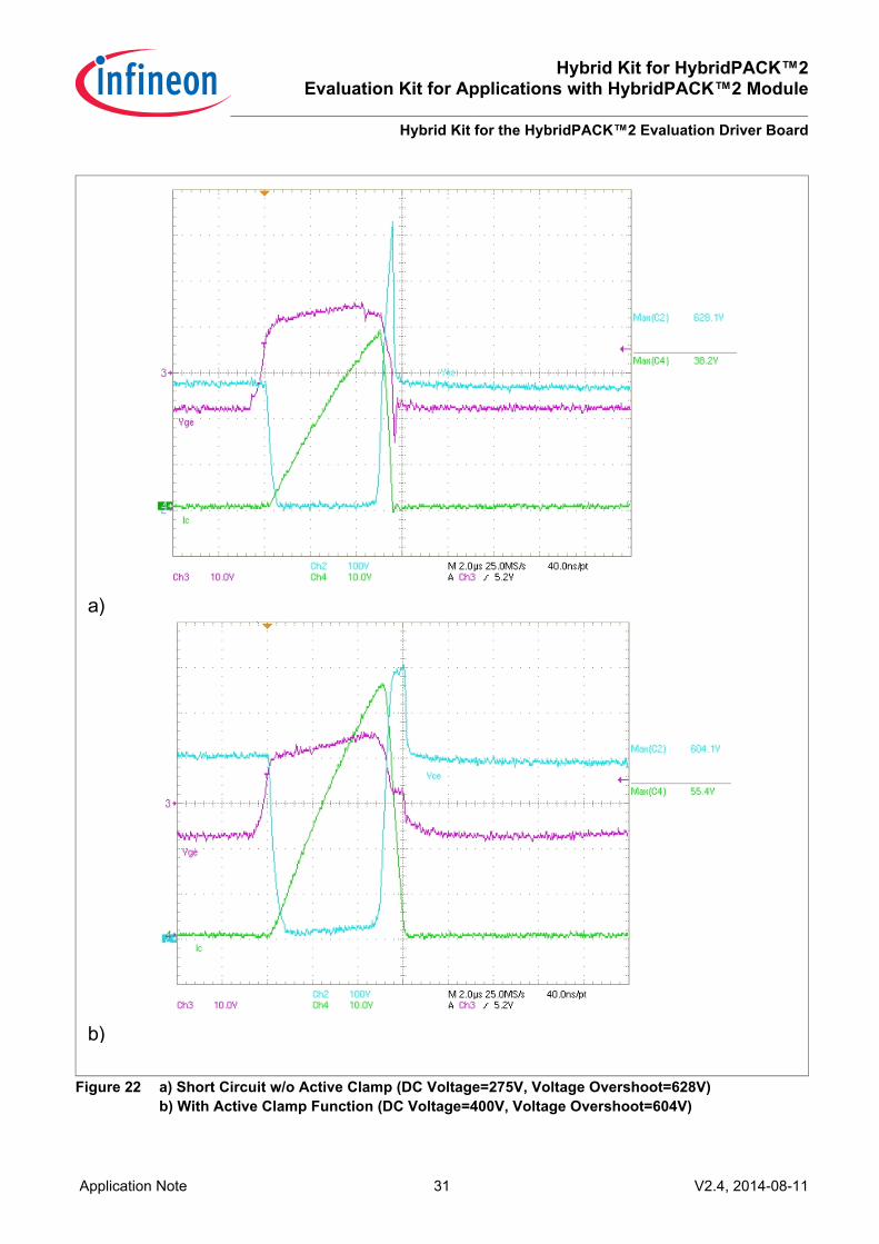
3.5.6 Short Circuit Protection and Clamp FunctionThe short circuit protection of the Driver Board basically relies on the detection of a voltage level higher as 9 V onthe DESAT pin of the 1ED020I12-FA driver IC and the implemented active clamp function. Thanks to this operationmode, the collector-emitter overvoltage, which is a result of the stray inductance and the collector current slope,is limited. Depending on the stray inductance, the current and the DC voltage the voltage overshoot during turnoff changes. Figure 21 shows the parts of the circuit needed for the desaturation function and the active clampingfunction.
Figure 21 Desaturation Protection and Active Clamping Diodes
In the case of a short circuit the collector-emitter saturation voltage will rise and the driver detects the short circuitoccurrence - to protect the IGBT it has to be turned off. As a consequence of IGBT turn-off process there will occuran voltage overshoot due to the stray inductance of the module and the DC-link. This voltage overshoot has to belower than the maximum IGBT blocking voltage. Therefore the Driver Board has an active clamping functionwhereby the clamping will increase the voltage for the booster and also increase the voltage directly on the gate.The typical turn-off waveform under short circuit condition and room temperature of a HybridPACK™2 modulewithout any additional protective functions is shown in Figure 22 a). Typical waveform under short circuit conditionwith active clamp function at room temperature is shown in Figure 22 b). As it can be seen, the voltage overshootwithout active clamping at a DC voltage of 275V is close to the maximum IGBT blocking voltage of HybridPACK™2(650V), which could damage the devices. With active clamping the voltage overshoot can be reduced and the DCvoltage increased without damaging the IGBT module (at 400V DC voltage can be observed voltage overshoot ofapproximately 604V, Figure 22 b). In design are implemented 510V clamping diodes. The level of the clampingvoltage must be adjusted depending on the application.
Hybrid Kit for HybridPACK™2Evaluation Kit for Applications with HybridPACK™2 Module
Hybrid Kit for the HybridPACK™2 Evaluation Driver Board
Application Note 31 V2.4, 2014-08-11
Figure 22 a) Short Circuit w/o Active Clamp (DC Voltage=275V, Voltage Overshoot=628V)b) With Active Clamp Function (DC Voltage=400V, Voltage Overshoot=604V)
a)
b)

Hybrid Kit for HybridPACK™2Evaluation Kit for Applications with HybridPACK™2 Module
Hybrid Kit for the HybridPACK™2 Evaluation Driver Board
Application Note 32 V2.4, 2014-08-11
3.5.7 Fault OutputWhen a short circuit occurs the voltage VCE is detected by the desaturation protection of the 1ED020I12-FA andthe IGBT is switched off. The fault is reported to the primary side of the driver as long as there is no reset signalapplied to the driver. The fault signal (/FLT) is active low - the schematic of design implemented in Driver Boardcan be seen on Figure 23.
Figure 23 Fault Output of a Single Driver IC
Figure 24 Fault Output During: a) Normal Operation b) Operation under Short Circuit
The fault signal (/FLT) will be in low state if a short circuit occurs and will remain low until /RST signal is pulleddown. On the Driver Board each of the three legs has its own fault signal (FAULTUn, FAULTVn, FAULTWn). As it canbe seen in Figure 31, a LED will warn in the case of a DESAT-FAULT condition in one of the phases. The threefault signals are connected to a logical AND gate and the output of this gate, together with the 3 phases faultsignals, is forwarded to the external connector (K1).
a) b)
Short circuit occurs
UGE
Fault signal
Ready signal

Hybrid Kit for HybridPACK™2Evaluation Kit for Applications with HybridPACK™2 Module
Hybrid Kit for the HybridPACK™2 Evaluation Driver Board
Application Note 33 V2.4, 2014-08-11
3.5.8 Temperature MeasurementThe IGBT module HybridPACK™2 includes three integrated NTC (Negative Temperature Coefficient) sensorswhich simplify the thermal measurements in inverters significantly. The NTCs are located on the same ceramic substrate together with the IGBT and diode chips. The module is filledwith silicon gel for isolation purpose and under normal operation conditions the requirements for isolation voltagesare met. The NTC isolation capability is tested with 2.5kV AC in final test for 1 minute for 100% of moduleproduction. The NTCs are connected to the main connector K1 (pins 10, 15 and 19) by means of the circuit showed inFigure 36. Figure 25 shows the relationship between IGBT module base plate temperature of the three phasesand output voltage of IGBT module temperature block (TEMP_IGBT_U, TEMP_IGBT_V, TEMP_IGBT_W,K3.10/K3.19/K3.15)
Figure 25 Characteristics of the Temperature Measurements
Note: This temperature measurement is not suitable for the short circuit or short term overload detection andshould be used only for the module protection against long term overload or malfunction of the cooling system.
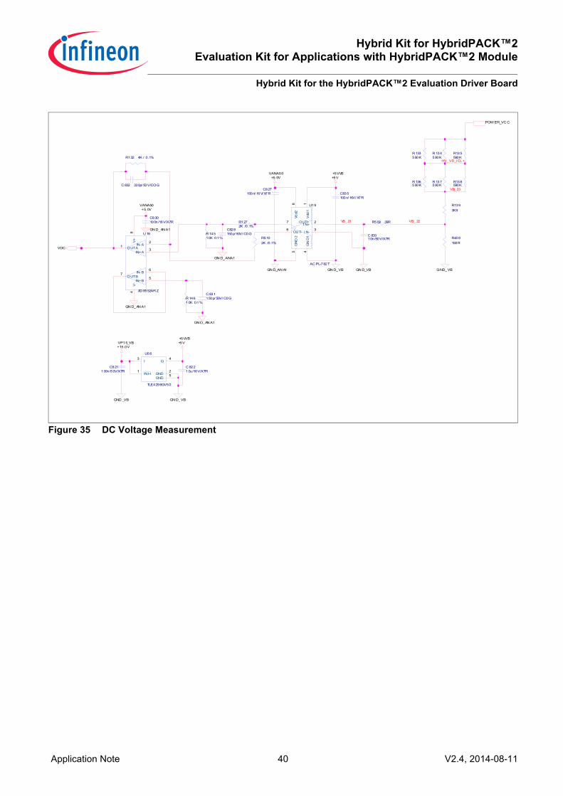
3.5.9 DC Voltage MeasurementOn the Hybrid Kit for HybridPACK™2 the voltage at the DC link is measured by means of a isolation amplifierwhich offers the necessary galvanic isolation (see Figure 35). The output of this circuit is connected to the external connector (Vdc, K1.9). Figure 26 shows the relationshipbetween DC link voltage and Vdc output signal.
Temperature Measurement
2,5
2,7
2,9
3,1
3,3
3,5
3,7
3,9
4,1
4,3
4,5
-30 -10 10 30 50 70 90 110
Temperature IGBT Module (°C)
Out
put v
olta
ge T
EMP_
IGB
T (V
)

Hybrid Kit for HybridPACK™2Evaluation Kit for Applications with HybridPACK™2 Module
Hybrid Kit for the HybridPACK™2 Evaluation Driver Board
Application Note 34 V2.4, 2014-08-11
Figure 26 Characteristics of the DC Voltage Measurement
3.6 Switching LossesSwitching losses can be different comparing to the values given in the HybridPACK™2 IGBT module datasheet.Main reason for this discrepancy is that switching voltages used on the Driver Board (+15V for turn-on and -8V forturn-off) differ from HybridPACK™2 characterisation switching voltages (+15V/-15V).Turn-on losses are expected to be close to the values of the datasheet of HybridPACK™2, but as mentioned, thiswill be different for the turn-off losses. In general the turn-off losses depend on the stray inductances of the DC-link and increase linear with the DC-link voltage. In the case of the Driver Board the turn-off losses do not increaselinearly because of the fact that the active clamping feature increases the turn-off losses due to decrease of thedi/dt.
3.7 Definition of Layers of Driver BoardThe Driver Board was made keeping the following rules for the copper thickness and the space between differentlayers shown in Figure 27.
Figure 27 Copper and Isolation for Layers of Driver Board
Vdc Vs. DC-Link Voltage
y = 0,0071x + 1,3296
0
0,5
1
1,5
2
2,5
3
3,5
4
4,5
0 50 100 150 200 250 300 350 400
DC-Link Voltage (V)
Vdc
(V)
Copper Isolation
1: 35 µm
2: 35 µm
3: 35 µm
4: 35 µm
5: 35 µm
1
2
3
4
5
6 6: 35 µm
1
2
3
4
5
6
1-2: 0.5 mm 2-3: 0.5 mm 3-4: 0.5 mm 4-5: 0.5 mm 5-6: 0.5 mm

Hybrid Kit for HybridPACK™2Evaluation Kit for Applications with HybridPACK™2 Module
Hybrid Kit for the HybridPACK™2 Evaluation Driver Board
Application Note 35 V2.4, 2014-08-11
3.8 Schematics, Layout and Bill of Material To meet the individual customer requirements and to make the Driver Board for the HybridPACKTM2 module as aplatform for development or modifications, all necessary technical data like schematics, layout and componentsare included in this chapter.
3.8.1 Schematics
Figure 28 Schematics Block Overview
IGBT_MODULE
IGBT_MODULE
COLWT
POW
ER_V
CC
COLUT
GN DUT
GN DUB
COLVT
GN DVT
GN DVB
GN DWT
GN DWB
GU T
GVT
GWT
GU B
GVB
GWB
Tem
p0
Tem
p1
Tem
p2T
emp3
Tem
p4Te
mp5
COLWB
COLVB
COLUB
DC-LINK_VOL_MEAS
DC-LINK_VOL_MEAS
VDC POWER_VCC
FAULTVn
VP15_VT+15.0V
VP15_U B+15.0V
VP15_WT+15.0V
GND_UB
GND_VT
VN8_UB-8.0V
VN 8_VT-8. 0V
VN 8_WT-8. 0V
GND_WT
VP15_U T+15.0V
GND_UT
VN 8_UT-8. 0V
FAULTW n
IGBT_DRIVER_UB
IGBT_DRIVER_UB
VPI N+
FLTn
I N-R STn G
COL
VNGN D
SMPS
SMPS12Vin
GNDUT
R STn
TEMP_IGBT_VTEMP_IGBT_UTEMP_IGBT_W
TEMP
TEMP
Temp0Temp1TEMP_I GBT_U
TEMP_I GBT_V Temp2Temp3
TEMP_I GBT_W
Temp4Temp5
Temp0Temp1
VP15_VB+15.0V
GND _DIG1
VN 8_VB-8.0V
GND_VB
Temp2
VP15_WB+15.0V
VN8_WB-8.0V
GND_WB
FAU LT_n
Temp3Temp4Temp5
GUT
COLUBGUBGUB
GNDUBGNDUB
IGBT_DRIVER_VT
IGBT_DRIVER_VT
VPI N+
FLTn
I N-R STn G
COL
VNGN D
GVTGNDVT
COLVBGVBGVB
GNDVB
COLWTGWT
GNDWT
GWB
C OLVT
PWMUTPWMUBPWMVT
COLU T
PWMVB
IGBT_DRIVER_WB
IGBT_DRIVER_WB
VPI N+
FLTn
I N-R STn G
COL
VNGN D
PWMWT
GNDWB
PWMWB
IGBT_DRIVER_UT
IGBT_DRIVER_UT
VPI N+
FLTn
I N-R STn G
COL
VNGN D
PWM_UTPWM_UBPWM_VT
I NPUT_LOGIC
I NPUT_LOGIC
PW M_WTPW M_WB
PW M_VTPW M_VB
PW M_UTPW M_UB
PWMWTPWMWB
PWMVTPWMVB
PWMUTPWMUB
PWM_VBPWM_WTPWM_WB
RSTn_in
VDC_meas_uc
IGBT_DRIVER_WT
IGBT_DRIVER_WT
VPI N+
FLTn
I N-R STn G
COL
VNGN D
FAULT_LOGI C
FAULT_LOGI C
FAULTUnFAULTVnFAU LTWn
RST_I NnRSTn
FAULT_WnFAULT_VnFAULT_Un
FAULT_n
CONNECTOR
CONNECTOR
R ST_INn
FLTWn
FLTUn
FLTn
PWMVBPWMWTPWMWB
PWMUTPW MUB
12V
GND _DIG
TEMP_IGBT_U
VDC
PWMVT
FLTVn
TEMP_IGBT_V
TEMP_IGBT_W
COLWB
IGBT_DRIVER_VB
IGBT_DRIVER_VB
VPI N+
FLTn
I N-R STn G
COL
VNGN D
FLTUnFLTVn
FAULTU n
FLTWn

Hybrid Kit for HybridPACK™2Evaluation Kit for Applications with HybridPACK™2 Module
Hybrid Kit for the HybridPACK™2 Evaluation Driver Board
Application Note 36 V2.4, 2014-08-11
Figure 29 SMPS - Power Supply
Figure 30 External Connector
Q5
IPD144N06NG
1
2
3
Q10IPD90P03P4L-04
WB_PS
R20159K
R18
7 19K
6
R19
4 0R02
5
C88
610
n/50
V/X
7R
GND_DIG1
UB_PS
GND_UB
R19
71k
6
R19
61k
6
V z =1 5 V
R19
81k
6
+
C88822u/35V
C8874u7/50V/X7R
C8894u7/25V/X7R
GND_UB
VP15_UB+15.0V
D17
1SMA5929BT3G
VN8_UB-8.0V
D16
ES1A
GND_DIG1
UNDER_VOL_DETECTION
UNDER_VOL_DETECTION
POWER_UPVP
12Vin
C88110n/50V/X7R
GND_DIG1
R2810K
V z= 1 5V
GND_DIG1
R16
91k
6
VB_PS
R17
01k
6
R17
11k
6
GND_DIG1
C891100n/16V/X7R
GND_DIG1 GND_DIG1
GND_DIG1
T1
TRANSFORMER2
1
2
3
45
67
89
1011
1213
1415
16
+
C86722u/35V
C8664u7/50V/X7R
C8684u7/25V/X7R
VT_PS
R18210K
WT_PS
V z= 1 5V
R17
31k
6
R17
41k
6
R17
51k
6
+
C87022u/35V
C8694u7/50V/X7R
C8714u7/25V/X7R
D7
1SMA5929BT3G
GND_DIG1
V z= 1 5V
R17
81k
6
R17
91k
6
R18
01k
6
+
C87322u/35V
C8724u7/50V/X7R
C8744u7/25V/X7R
D9
1SMA5929BT3G
R18
31k
6
Vz = 15 V
R18
51k
6
R18
61k
6
+
C87922u/35V
D5
1SMA5929BT3G
C8774u7/50V/X7R
UT
_PS
C8804u7/25V/X7R
+
C89022u/16V/X7R
D13
1SMA5929BT3G
GND_DIG1
VP15_UT+15.0V
VP15_WB+15.0V
VP15_VT+15.0V
VP15_WT+15.0V
GND_VT
GND_UT
GND_WB
VN8_UT-8.0V
VN8_WB-8.0V
VN8_VT-8.0V
VN8_WT-8.0V
D4
ES1A
GND_WT
D6
ES1A
D8
ES1A
D11
ES1A
R199
0R
Vz = 15 V
R19
11k
6
R19
01k
6
R19
21k
6
C8824u7/50V/X7R
D18
ES1A
+
C88322u/35V
C8854u7/25V/X7R
D15
1SMA5929BT3G
GND_VB
VP15_VB+15.0V
D14
ES1A
VN8_VB-8.0V
GND_DIG1
C878100nF/100V/X7R
GND_DIG1
D10ES1A
VDIG50+5.0V
+
C87
5
4u7/
50V
/X7R
+
C876100µF/20V/0810
GND_DIG1 GND_DIG1
+
C90722u/16V/X7R
D121SMB5935BT3
R184 80K6
U30
LM3478MM
Isen1
COMP2
FB3
AGND4
PGND5
DR6FA/SD
7Vin
8
R19
34k
75
D19
BZV55/C13
GND_DIG1
1 0k
1 0k
Q13ABCR10PN
5
2
6
1
D201SMB30AT3
R533
0R
R534
opt
L1
MURATA_BLM21P221SN
805
GND_ANA1
C906100n/50V/X7R
VANA50+5.0V10 k
10 k
Q13BBCR10PN
5
5
3
4
C88
422
n/50
V/X
7R
K1
TW-12-06-L-D -475-SM-A
11
22
33 4 4
55
66
77
88
99
1010
1111 12 12
1313
1414
1515
1616
1717
1818
1919 20 20
2121
2222
2323
2424
PWMWTRST_IN n
PWMVBPWMVTPWMWB
PWMU BPWMU T
VDC
FLTVn
FLTWnTEMP_BOAR D
FLTnFLTU n
VAN A50_DB
TEMP_H P2_V
TEMP_H P2_W
TEMP_HP2_U
KL_30+12.0V
GN D_DI G1
KL_30+12. 0V
GN D_DI G1GN D_AN A1

Hybrid Kit for HybridPACK™2Evaluation Kit for Applications with HybridPACK™2 Module
Hybrid Kit for the HybridPACK™2 Evaluation Driver Board
Application Note 37 V2.4, 2014-08-11
Figure 31 Fault Logic
R51
7 220R
10k
1 0k
Q 12B
BC R 183S
P A C KA GE = 1
5
4
3
R51
9 220R
R 515
15K
R 514 1K
R 513
15K
D21
D23
R51
8 220R
C 89810n/ 50V/ X7R
U 57
74LV C 1G11GW
A1
GN D2
B3
Y4
Vc c 5
C6
R 516 1K
10k
1 0k
Q 12A
B C R 183S
P AC KA GE = 1
2
1
6
R 512 1K
D22
R 511
15K
C 89910n/ 50V/ X7R
10k
1 0k
Q 11B
BC R 183S
P A C KA GE = 2
5
4
3
C 89610n/ 50V/ X7R
C 897100n/ 50V /X7R
10k
1 0k
Q11A
BC R 183S
P AC KA GE = 2
2
1
6
FA U LTU n
FA U LTW n
FA U LTVn
F AU LT_W n
R STn R S T_IN n
F AU LT_nF AU LT_U n
F AU LT_V n
V D I G50+5. 0V
GN D _D I G1
V D IG 50+5.0V
GN D _D I G1GN D _D IG 1
GN D _D I G1
GN D _D I G1
V D I G50+5. 0V
VD IG 50+5.0V
V D I G50+5. 0V
GN D _D I G1 GN D _D I G1
VD IG 50+5.0V
VD IG50+5.0V
GN D _D I G1
VD I G50+5. 0V

Hybrid Kit for HybridPACK™2Evaluation Kit for Applications with HybridPACK™2 Module
Hybrid Kit for the HybridPACK™2 Evaluation Driver Board
Application Note 38 V2.4, 2014-08-11
Figure 32 Input Logic
C900100pF/100V/COG
R520100R
GND_DIG1
R52115k
GND_DIG1
C901100pF/100V/COG
R522100R
GND_DIG1
R52315k
GND_DIG1
C902100pF/100V/COG
R524100R
GND_DIG1
R52515k
GND_DIG1
C903100pF/100V/COG
R526100R
GND_DIG1
R52715k
GND_DIG1
C904100pF/100V/COG
R528100R
GND_DIG1
R52915k
GND_DIG1
C905100pF/100V/COG
R530100R
GND_DIG1
R53115k
GND_DIG1
PWM_WT
PWM_WB
PWM_VT
PWM_VB
PWM_UT
PWM_UB
PWMWT
PWMWB
PWMVT
PWMVB
PWMUT
PWMUB
Hybrid Kit for HybridPACK™2Evaluation Kit for Applications with HybridPACK™2 Module
Hybrid Kit for the HybridPACK™2 Evaluation Driver Board
Application Note 39 V2.4, 2014-08-11
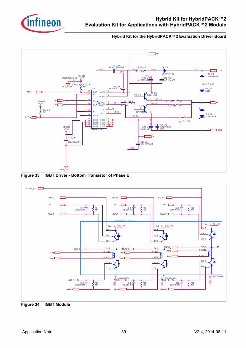
Figure 33 IGBT Driver - Bottom Transistor of Phase U
Figure 34 IGBT Module
U 4
1E D 020I12-FA
V EE 21
D E SA T3
GN D 2 4N C
5
V C C 2 6
OU T 7
C LAMP 8
V EE 22
GN D 119
I N +13
I N -14
R D Y15
/ FLT16 / R ST17
V C C 118
GN D 120 V EE 2 9
V EE 2 10GN D 1
11 GN D 112
D 3_U BP6S MB510A
C 20_U B4u7/ 25V/ X7R
R 29_U B4k 7
R 14_U B0R
R 33_U B 2R 7
R 28_U B
1K
R 32_U B 2R 7
R 34_U B4k7
T2_U B
ZXTP 2012Z
1
3
2
C 23_U B100n/ 50V/ X7R
C 17_U B100n/ 50V/ X7R
C 14_U B
100pF/ 100V / C OG
C 13_U B100pF /100V /C OG
C 21_U B4u7/ 25V /X7R
C 22_U B
100n/ 50V / X7R
D 4_U BE S1D
T1_U BZXTN 2010Z1
2
3
R 31_U B
47R
D 9_U BS MBJ 14C A
C 16_U B4u7/ 25V/ X7R
D 6_U B
MU R A160T3G
C 15_U B4u7/ 25V /X7R
VP
FLTn
I N +G
R STn
I N -
GN D
V N
C OL
VD I G50+5. 0V
GN D _D I G1
GN D _D I G1
V D I G50+5. 0V
VD IG50+5.0V
U B_07
U B _05
GN D
U B _04
GN DGN D
GN D
GN D
GN D
U B_01 C OL
U B_06
U B_02
H V _U B_U SD
U B _03
Q4C
FS800R 06KE3
C W_T
CW _B
EW_T
GW_T
GW _B
EW _B
N3
W
P3
W _N TC 2
W _N TC 1
DC L+_P1 D CL+_P2DC L+_P3
DCL
-_N3
COLU B
C 7922n/50V/ X7R
DCL-
_N2
C OLVB
DCL
-_N
1
C OLWB
Temp5
R8210K
C 8022n/50V/ X7R
R 8310K
C8122n/ 50V/X7R
R8410K
C 8222n/50V/ X7R
R8510K
C 8322n/50V/ X7R
R 8610K
C8422n/ 50V/X7R
R8710K
HybridPACK2 - module
Temp2
Temp3
POWER _VC C
C OLWTC OLUT COLVT
GN DU B
GND UT
GN DVB
GN DVT
GUT
GND WB
GND WT
GU B
GWTGVT
GWBGVB
Temp1
Temp0Temp4
Q4A
FS800R06KE3
C U_T
CU _B
EU_T
GU_T
GU _B
EU _B
N1
U
P1
U _N TC 2
U _N TC 1
Q4B
FS800R06KE3
C V_T
CV_B
EV_T
GV_T
GV_B
EV_B
N2
V
P2
V_NTC2
V_NTC1
Hybrid Kit for HybridPACK™2Evaluation Kit for Applications with HybridPACK™2 Module
Hybrid Kit for the HybridPACK™2 Evaluation Driver Board
Application Note 40 V2.4, 2014-08-11
Figure 35 DC Voltage Measurement
R1272K /0.1%
C828150p/ 50V/ C0G
R509 39RVB_21
U 18
AD 8552AR Z
OUTA1 IN-A2
IN+A3
V-
4
IN+B5
IN-B6
OUTB7
V+
8
R5102K /0 .1%
R 133590K
R 134590K
R135590K
C830100n/16V/X7R
R 136590K
GN D_VB
R 137590K
GND_VB
R138590K
GND _VB
U19
AC PL-782T
OU T-6
I N+2
I N-3
GN
D1
4
GN
D2
5
Vdd
11
7 OUT+
Vdd2
8
GN D_VB
VB_23
VANA50+5. 0V
HV_VD_I CL+
GN D_VB
R1393K9
GN D_AN A1
R408158R
GN D_AN A1
U56
TLE4296GV50
IN H1
GND2
I3
Q4
GND5
VP15_VB+15.0V
+5VVB+5V
C 82210u/16V/X7R
C821100n/50V/X7R
C 83310n/50V/X7R
R 14510K 0.1%
VB_22
R132 4K / 0.1%
C 832 330p/ 50V/COG
C 831150p/ 50V/ C0GR 146
10K 0.1%
GN D_AN A1
C835100n/ 16V/ X7R
+5VVB+5V
VANA50+5. 0V
GN D_AN A1
POW ER_VC C
VDC
GN D_ANA1
C827100n/ 16V/ X7R

Hybrid Kit for HybridPACK™2Evaluation Kit for Applications with HybridPACK™2 Module
Hybrid Kit for the HybridPACK™2 Evaluation Driver Board
Application Note 41 V2.4, 2014-08-11
Figure 36 IGBT Module Temperature Measurement
TEMP _IGB T_U
Tem p3
Tem p2
GN D _A N A1
R 204 opt
R 206 0R
GN D _A N A1
GN D _A N A1
VA N A50+5.0V
GN D _AN A 1
C 89410n/ 50V/ X7R
U 33
A D 8552A R Z
O U TA1 IN -A 2
IN +A 3
V-4
IN +B5
IN -B 6
O U TB7
V+8 V AN A 50
+5. 0V
R20
310
K5/
1%R
205
10K
5/1%
G N D _AN A 1
Tem p0
Tem p1
VA N A50+5. 0V
R20
810
K5/1
%
GN D _AN A 1
R20
910
K5/1
%
GN D _AN A 1
R 210 opt
TEMP _IGB T_V
R 207 0R
Tem p4
Tem p5TE MP_I GBT_W
C 91010n/ 50V/ X7R
C 90810n/ 50V/ X7R
C 909
1u/ 16V/ X7R
C 91110n/ 50V/ X7R
C 91310n/ 50V/ X7R
C 912
1u/ 16V V/ X7R
C 91410n/50V / X7R
C 91610n/50V /X7R
C 915
1u/ 16V/ X7R
R 212 opt
GN D _A N A1
R 214 0R
GN D _AN A1
VA N A50+5. 0V
GN D _AN A 1
C89
5
10n/
50V/
X7R
U 34
AD 8552A R Z
OU TA1 IN -A 2
I N +A3
V-4
I N +B5
IN -B 6
OU TB7
V+8
VA N A50+5.0V
R21
110
K5/1
%R
213
10K5
/1%
GN D _A N A1
GN D _A N A1
GN D _A N A1
GN D _A N A 1

Hybrid Kit for HybridPACK™2Evaluation Kit for Applications with HybridPACK™2 Module
Hybrid Kit for the HybridPACK™2 Evaluation Driver Board
Application Note 42 V2.4, 2014-08-11
3.8.2 Assembly Drawing
Figure 37 Assembly Drawing of the Driver Board (Top) - part 1

Hybrid Kit for HybridPACK™2Evaluation Kit for Applications with HybridPACK™2 Module
Hybrid Kit for the HybridPACK™2 Evaluation Driver Board
Application Note 43 V2.4, 2014-08-11
Figure 38 Assembly Drawing of the Driver Board (Top) - part 2

Hybrid Kit for HybridPACK™2Evaluation Kit for Applications with HybridPACK™2 Module
Hybrid Kit for the HybridPACK™2 Evaluation Driver Board
Application Note 44 V2.4, 2014-08-11
Figure 39 Assembly Drawing of the Driver Board (Bottom) - part 1
Hybrid Kit for HybridPACK™2Evaluation Kit for Applications with HybridPACK™2 Module
Hybrid Kit for the HybridPACK™2 Evaluation Driver Board
Application Note 45 V2.4, 2014-08-11
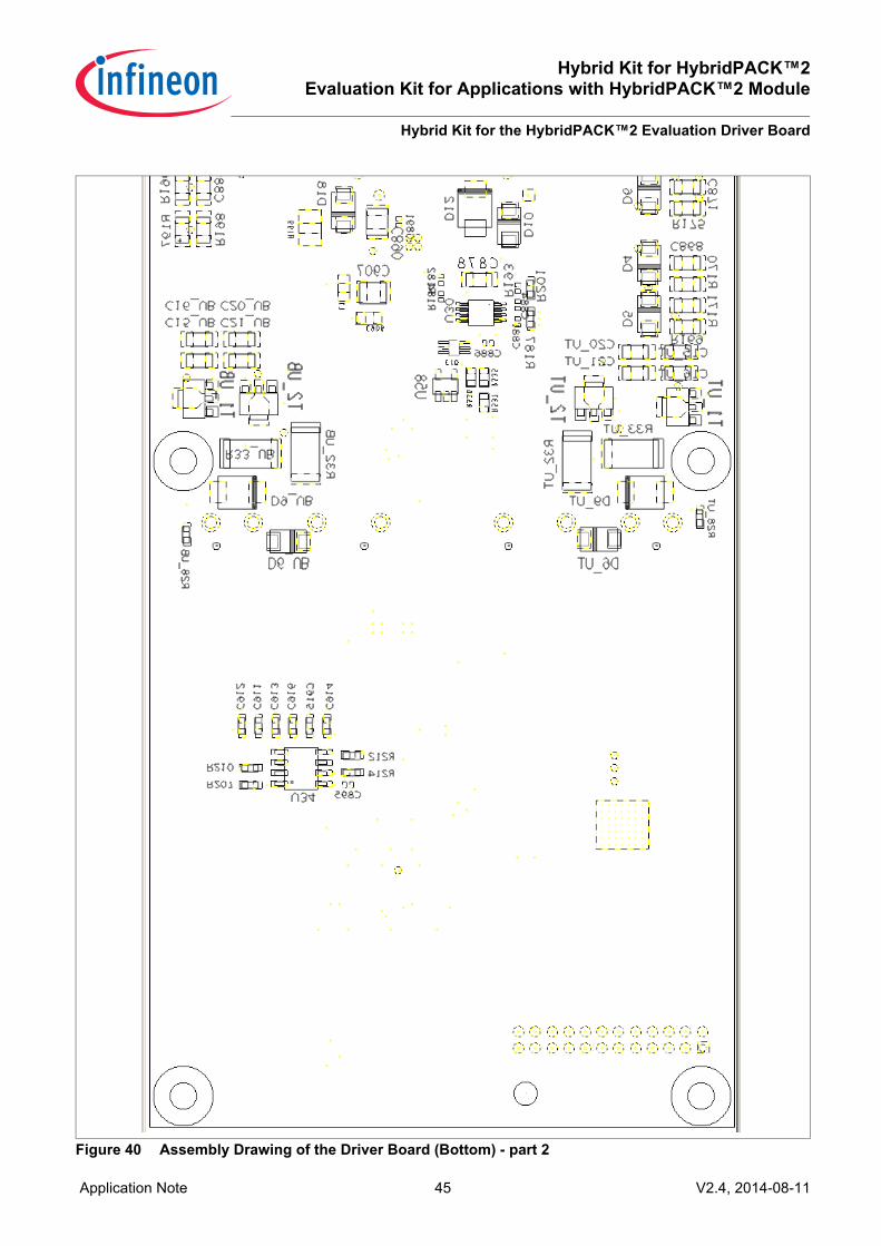
Figure 40 Assembly Drawing of the Driver Board (Bottom) - part 2

Hybrid Kit for HybridPACK™2Evaluation Kit for Applications with HybridPACK™2 Module
Hybrid Kit for the HybridPACK™2 Evaluation Driver Board
Application Note 46 V2.4, 2014-08-11
For detail information use the zoom function of your PDF viewer to zoom into the drawings on Figure 37,Figure 38, Figure 39 and Figure 40.
3.8.3 LayoutLayout of the Driver Board is shown on Figure 41 (Top Layer), on Figure 42 (Layer 2), on Figure 43 (Layer 3),on Figure 44 (Layer 4), on Figure 45 (Layer 5) and on Figure 46 (Bottom Layer).
Figure 41 Driver Board - Top Layer
Figure 42 Driver Board - Layer 2
Figure 43 Driver Board - Layer 3

Hybrid Kit for HybridPACK™2Evaluation Kit for Applications with HybridPACK™2 Module
Hybrid Kit for the HybridPACK™2 Evaluation Driver Board
Application Note 47 V2.4, 2014-08-11
Figure 44 Driver Board - Layer 4
Figure 45 Driver Board - Layer 5
Figure 46 Driver Board - Bottom Layer
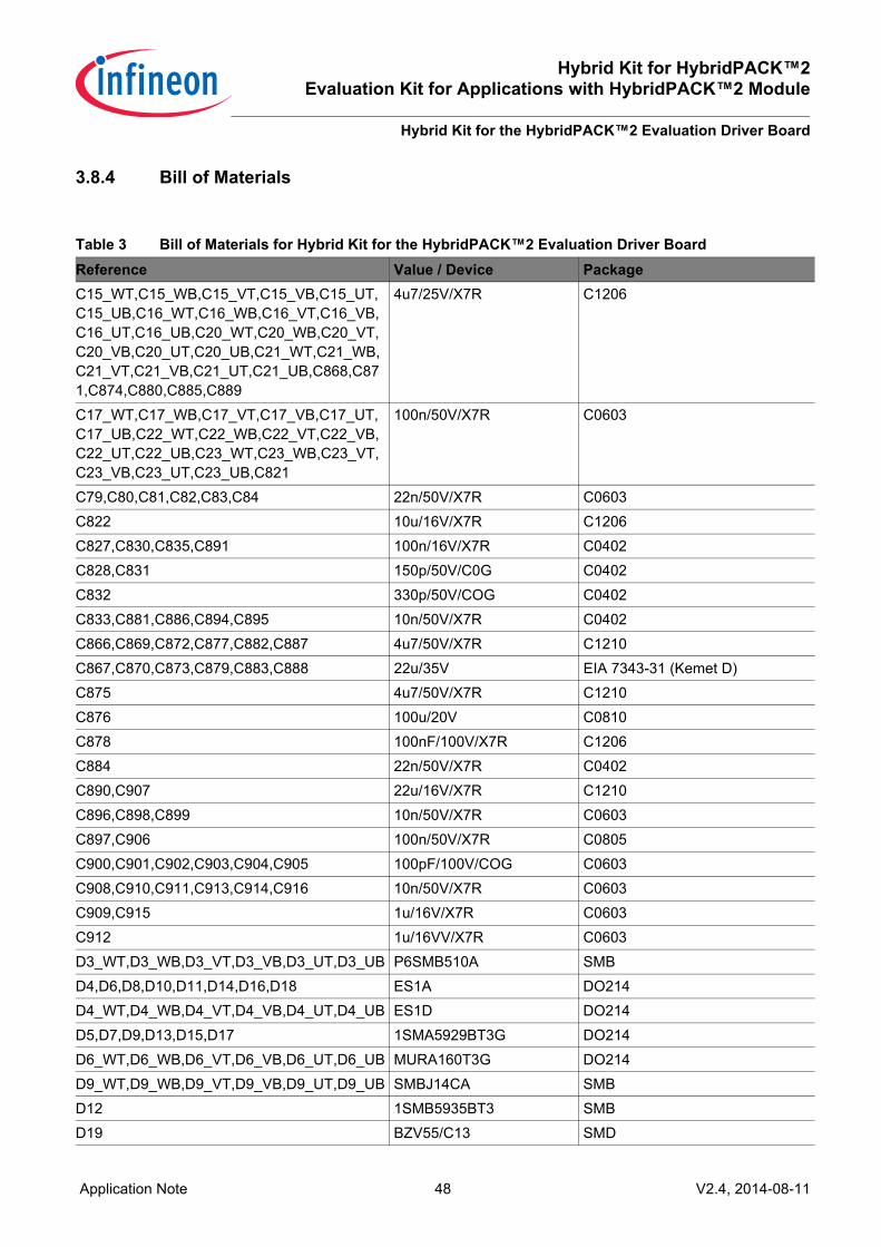
Hybrid Kit for HybridPACK™2Evaluation Kit for Applications with HybridPACK™2 Module
Hybrid Kit for the HybridPACK™2 Evaluation Driver Board
Application Note 48 V2.4, 2014-08-11
3.8.4 Bill of Materials
Table 3 Bill of Materials for Hybrid Kit for the HybridPACK™2 Evaluation Driver BoardReference Value / Device PackageC15_WT,C15_WB,C15_VT,C15_VB,C15_UT, C15_UB,C16_WT,C16_WB,C16_VT,C16_VB, C16_UT,C16_UB,C20_WT,C20_WB,C20_VT, C20_VB,C20_UT,C20_UB,C21_WT,C21_WB, C21_VT,C21_VB,C21_UT,C21_UB,C868,C871,C874,C880,C885,C889
4u7/25V/X7R C1206
C17_WT,C17_WB,C17_VT,C17_VB,C17_UT, C17_UB,C22_WT,C22_WB,C22_VT,C22_VB, C22_UT,C22_UB,C23_WT,C23_WB,C23_VT, C23_VB,C23_UT,C23_UB,C821
100n/50V/X7R C0603
C79,C80,C81,C82,C83,C84 22n/50V/X7R C0603C822 10u/16V/X7R C1206C827,C830,C835,C891 100n/16V/X7R C0402C828,C831 150p/50V/C0G C0402C832 330p/50V/COG C0402C833,C881,C886,C894,C895 10n/50V/X7R C0402C866,C869,C872,C877,C882,C887 4u7/50V/X7R C1210C867,C870,C873,C879,C883,C888 22u/35V EIA 7343-31 (Kemet D)C875 4u7/50V/X7R C1210C876 100u/20V C0810C878 100nF/100V/X7R C1206C884 22n/50V/X7R C0402C890,C907 22u/16V/X7R C1210C896,C898,C899 10n/50V/X7R C0603C897,C906 100n/50V/X7R C0805C900,C901,C902,C903,C904,C905 100pF/100V/COG C0603C908,C910,C911,C913,C914,C916 10n/50V/X7R C0603C909,C915 1u/16V/X7R C0603C912 1u/16VV/X7R C0603D3_WT,D3_WB,D3_VT,D3_VB,D3_UT,D3_UB P6SMB510A SMBD4,D6,D8,D10,D11,D14,D16,D18 ES1A DO214D4_WT,D4_WB,D4_VT,D4_VB,D4_UT,D4_UB ES1D DO214D5,D7,D9,D13,D15,D17 1SMA5929BT3G DO214D6_WT,D6_WB,D6_VT,D6_VB,D6_UT,D6_UB MURA160T3G DO214D9_WT,D9_WB,D9_VT,D9_VB,D9_UT,D9_UB SMBJ14CA SMBD12 1SMB5935BT3 SMBD19 BZV55/C13 SMD

Hybrid Kit for HybridPACK™2Evaluation Kit for Applications with HybridPACK™2 Module
Hybrid Kit for the HybridPACK™2 Evaluation Driver Board
Application Note 49 V2.4, 2014-08-11
D20 1SMB30AT3 SMBD21,D22,D23 LED_LSM676-MQ D0805K1 MMS-112-01-L-DV 24POLK1_opt,K2_opt,K3_opt,K4_opt,K5_opt,K6_opt JST 09HVD6B-EMGF-NR 09HVD6B-EMGF-NRL1 MURATA_BLM21P221SN L0805Q4 FS800R06KE3 HybridPACK™2Q5 IPD144N06NG TO252Q10 IPD90P03P4L-04 TO252Q11,Q12 BCR183S SOT363Q13 BCR10PN SOT363R14_WT,R14_WB,R14_VT,R14_VB,R14_UT, R14_UB,R206,R207,R214
0R R0603
R28_WT,R28_WB,R28_VT,R28_VB,R28_UT, R28_UB
1K R0603
R28 10K R0805R29_WT,R29_WB,R29_VT,R29_VB,R29_UT, R29_UB
4K7 R0603
R31_WT,R31_WB,R31_VT,R31_VB,R31_UT, R31_UB
47R R0805
R32_WT,R32_WB,R32_VT,R32_VB,R32_UT, R32_UB,R33_WT,R33_WB,R33_VT,R33_VB, R33_UT,R33_UB
2R7 R2512
R34_WT,R34_WB,R34_VT,R34_VB,R34_UT, R34_UB,R193
4k75 R0402
R82,R83,R84,R85,R86,R87,R182 10K R0402R127,R510 2K /0.1% R0603R132 4K / 0.1% R0603R133,R134,R135,R136,R137,R138 590K R1206R139 3K9 R0603R145,R146 10K 0.1% R0603R169,R170,R171,R173,R174,R175,R178,R179,R180,R183,R185,R186,R190,R191,R192,R196,R197,R198
1k6 R1206
R184 80K6 R0402R187 19K6 R0603R194 0R025 R2010R199,R533 0R R1210R201 59K R0603R203,R205,R208,R209,R211,R213 10K/1% R0603R204,R210,R212 opt R0603
Table 3 Bill of Materials for Hybrid Kit for the HybridPACK™2 Evaluation Driver Board (cont’d)
Reference Value / Device Package

Hybrid Kit for HybridPACK™2Evaluation Kit for Applications with HybridPACK™2 Module
Hybrid Kit for the HybridPACK™2 Evaluation Driver Board
Application Note 50 V2.4, 2014-08-11
R408 158R R0603R509 39R R0603R511,R513,R515,R521,R523,R525,R527,R529,R531
15k R0603
R512,R514,R516 1K R0603R517,R518,R519 220R R0603R520,R522,R524,R526,R528,R530 100R R0603R534 opt R1210R535 226K R0603R536 5K1 R0603R537 47K R0603T1 TRANSFORMER2T1_WT,T1_WB,T1_VT,T1_VB,T1_UT,T1_UB ZXTN2010Z SOT89T2_WT,T2_WB,T2_VT,T2_VB,T2_UT,T2_UB ZXTP2012Z SOT89U4,U5,U6,U7,U8,U9 1ED020I12-FA PG-DSO-20U18,U33,U34 AD8552ARZ SO-8U19 ACPL-782T DIP-8U30 LM3478MM MSOP-8U56 TLE4296GV50 SCT595U57 74LVC1G11GW SOT363U58 MAX6457UKD3A-T SOT23-5
Table 3 Bill of Materials for Hybrid Kit for the HybridPACK™2 Evaluation Driver Board (cont’d)
Reference Value / Device Package

Hybrid Kit for HybridPACK™2Evaluation Kit for Applications with HybridPACK™2 Module
Hybrid Kit for the HybridPACK™2 Logic Board
Application Note 51 V2.4, 2014-08-11
4 Hybrid Kit for the HybridPACK™2 Logic BoardLogic Board contains all components for the control of the Hybrid Kit for the HybridPACK™2. Furthermore itprovides the interface for all the others elements which build a complete inverter system: motor interface (encoder,resolver, GMR or hall sensor), current sense interface, communication (CAN and RS232) and additional analogueand digital inputs/outputs. It is supported in 2 versions: version v1.2 on Figure 47 (not produced anymore) andversion v1.3b on Figure 48. Figure 49 shows the block structure of the Logic Board and the following chaptersdescribe these blocks in detail. Although the block structure shown on Figure 49 can be applied on both versions,v1.2 and v1.3b are different in a few details. Comparing to v1.2 the Logic Board v1.3b is a further step in thedevelopment of the Hybrid Kit that offers some new features to the customer - the most important is GMR interfacedetailed described in Chapter 4.10.New features on Logic Board v1.3b comparing to v1.2 are following:• On-Board (on the bottom of the Logical Board) temperature measurements (Figure 78);• Usage of Infineon Technologies TLE7368E Micro Controller Power Supply IC (Figure 63);• Added some reference power supply for MCU A/D converters;• Implemented parallel communication interface on resolver chip AD2S1200YST (IC8 on Figure 67) and added
belonging circuitry (see Figure 69);• Added more options for trimming the resolver signal and added test points for measuring resolver signals;• Implemented differential signaling to the encoder interface (instead of single ended interface as it was in v1.2);• Improved phase current sense filtering - adapted to filter signals up to 5kHZ cut-off frequency by means of
second order filter (Figure 74);• Adapted filtering on DC-Bus voltage measuring signals, temperature sensing signals, emulated encoder
outputs of resolver chip (Figure 74);• Removed one general purpose digital I/O due to leak of pins on the connector;• Due to added differential signaling and GMR interface the external interface 34-pin connector is replaced with
50-pin connector; (Figure 50 and Figure 51);

Hybrid Kit for HybridPACK™2Evaluation Kit for Applications with HybridPACK™2 Module
Hybrid Kit for the HybridPACK™2 Logic Board
Application Note 52 V2.4, 2014-08-11
Figure 47 Hybrid Kit for the HybridPACK™2 Logic Board v1.2

Hybrid Kit for HybridPACK™2Evaluation Kit for Applications with HybridPACK™2 Module
Hybrid Kit for the HybridPACK™2 Logic Board
Application Note 53 V2.4, 2014-08-11
Figure 48 Hybrid Kit for the HybridPACK™2 Logic Board v1.3b
Figure 49 Block Diagram of the Logic Board
Logic Board
HybridPACKTM 2 Driver Board
PWM
Temp. IGBT (x3)
FAULTSignals
Current U
RST
VDC Meas.
SupplyC
on
ne
ct
or
Co
nn
ec
to
r
Connector
Current V
Current W
CAN
EncoderResolver
Supply Debug
Connector
MicrocontrollerTC1767
CAN / RS232
Resolver
A/D IO
Other Sensor
Supply
Watchdog
LevelShifter
VDC, Temp
Other sensor
RS232
EEPROM
Resolver InterfaceI, U, V Current
Measurement
Encoder

Hybrid Kit for HybridPACK™2Evaluation Kit for Applications with HybridPACK™2 Module
Hybrid Kit for the HybridPACK™2 Logic Board
Application Note 54 V2.4, 2014-08-11
4.1 External Connector Pin AssignmentLogic Board external connector X1-SIG1 (Harwin M80-5123442 on Logic Board v1.2) or K2 (Harwin M80-5125042P on Logic Board v1.3b) provides the interface to all the external systems: motor (encoder, resolver, Hallsensor or GMR), current sense, communication (CAN and RS232) and extra analogue and digital inputs/outputs.Figure 50 and Table 4 are showing the pin assignment of the connector X1-SIG1 for the Logic Board v1.2.Figure 51 and Table 5 are showing the pin assignment of the connector K2 for the Logic Board v1.3b. The femalepart for 34-pin connector Harwin M80-5123442 (Logic Board v1.2) is socket Harwin M80-4603442. The femalepart for 50-pin connector Harwin M80-5125042P (Logic Board v1.3b) is socket Harwin M80-4605042.
Figure 50 External Connector Pin Assignment Logic Board v1.2
Table 4 External Connection Pin Assignment Logic Board v1.2Pin Number Pin Name Type Description1 ADC_IN1 I/O General Purpose Analog I/O2 StatorTemp Input Motor Temperature Measurement3 ADC_IN2 I/O General Purpose Analog I/O4 PosA Input Encoder Phase A
2
10
14
18
4
8
12
16
20
StatorTemp
PosA
PosB
PosZ
PosU
PosV
PosW
S6
S2
6
1
9
13
17
3
7
11
15
19
5
21
29
33
23
27
31
25
22
30
34
24
28
32
26
S3
S1
R1
R2
DIO_2
DIO_1
I_W
VDIG5.0
CAN1_L
CAN1_H
ASC_RX
ASC_TX
+12.0V
GND_DIG1
VANA5.0
GND_ANA1
I_V
I_U
ADC_IN1
ADC_IN2
ADC_IN3
+12.0V
DIO_4
DIO_3
GND_DIG1
Motor Interface (Encoder)
Motor Interface(Resolver)
Phase Current Sense
Communication
General Purpose Ana/Dig IN/OUT
Power Supply
Motor Interface (Hall Sensor)
Bottom View on Crimp Connector M80-4603442 (counterpart on Logic Board v1.2 M80-5123442)
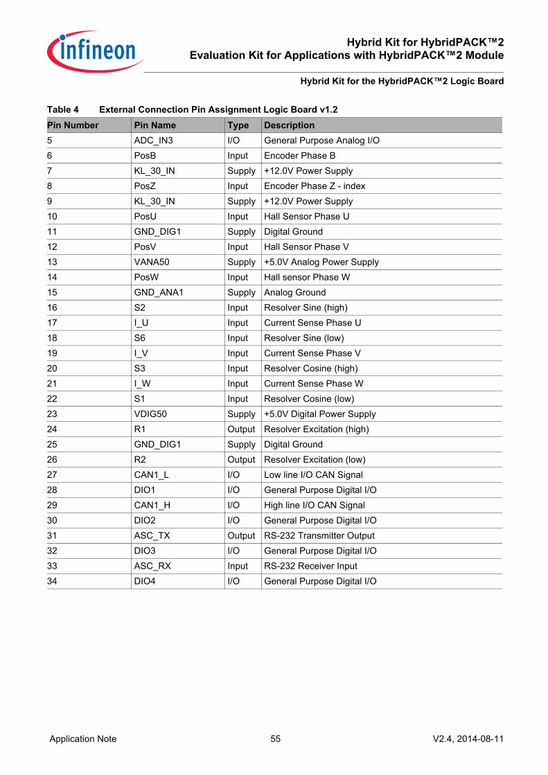
Hybrid Kit for HybridPACK™2Evaluation Kit for Applications with HybridPACK™2 Module
Hybrid Kit for the HybridPACK™2 Logic Board
Application Note 55 V2.4, 2014-08-11
5 ADC_IN3 I/O General Purpose Analog I/O6 PosB Input Encoder Phase B7 KL_30_IN Supply +12.0V Power Supply8 PosZ Input Encoder Phase Z - index9 KL_30_IN Supply +12.0V Power Supply10 PosU Input Hall Sensor Phase U11 GND_DIG1 Supply Digital Ground12 PosV Input Hall Sensor Phase V13 VANA50 Supply +5.0V Analog Power Supply14 PosW Input Hall sensor Phase W15 GND_ANA1 Supply Analog Ground16 S2 Input Resolver Sine (high)17 I_U Input Current Sense Phase U18 S6 Input Resolver Sine (low)19 I_V Input Current Sense Phase V20 S3 Input Resolver Cosine (high)21 I_W Input Current Sense Phase W22 S1 Input Resolver Cosine (low)23 VDIG50 Supply +5.0V Digital Power Supply24 R1 Output Resolver Excitation (high)25 GND_DIG1 Supply Digital Ground26 R2 Output Resolver Excitation (low)27 CAN1_L I/O Low line I/O CAN Signal28 DIO1 I/O General Purpose Digital I/O29 CAN1_H I/O High line I/O CAN Signal30 DIO2 I/O General Purpose Digital I/O31 ASC_TX Output RS-232 Transmitter Output32 DIO3 I/O General Purpose Digital I/O33 ASC_RX Input RS-232 Receiver Input34 DIO4 I/O General Purpose Digital I/O
Table 4 External Connection Pin Assignment Logic Board v1.2Pin Number Pin Name Type Description

Hybrid Kit for HybridPACK™2Evaluation Kit for Applications with HybridPACK™2 Module
Hybrid Kit for the HybridPACK™2 Logic Board
Application Note 56 V2.4, 2014-08-11
Figure 51 External Connector Pin Assignment Logic Board v1.3b
2
10
14
18
4
8
12
16
20
StatorTemp
PosA/iGMR_A+
PosA/iGMR_A-
PosB/iGMR_B+
iGMR_CSn+
iGMR_DATA-
iGMR_DATA+
S6
S2
6
1
9
13
17
3
7
11
15
19
5
21
29
33
23
27
31
25
22
30
34
24
28
32
26
S3
S1
R1
R2
DIO_2
DIO_1
I_W
VDIG50
CAN1_L
CAN1_H
ASC_RX
ASC_TX
GND_ANA1
VANA50
GND_ANA1
I_V
I_U
ADC_IN1
ADC_IN2
ADC_IN3
DIO_3
GND_DIG1
Motor Interface (Encoder)
Motor Interface(Resolver)
Phase Current Sense
Communication
General Purpose Ana/Dig IN/OUT
Power Supply
Motor Interface (Hall Sensor)
Bottom View on Crimp Connector M80-4605042 (counterpart on Logic Board v1.3b M80-5125042P)
iGMR_Ren_DE+
iGMR_CSn-
iGMR_Ren_DE-
PosB/iGMR_B-
PosZ/iGMR_Z+
PosZ/iGMR_Z-
PosU/iGMR_U
PosV/iGMR_V
PosW/iGMR_W
37
35
41
39
45
43
GND_DIG1
47
49
VDIG50
iGMR_CLK-
iGMR_CLK+
38
36
40
+12V
GND_DIG1
GND_DIG1
+12V
GND_DIG1
42
46
44
48
50
Motor Interface (iGMR Sensor)
Not Connected

Hybrid Kit for HybridPACK™2Evaluation Kit for Applications with HybridPACK™2 Module
Hybrid Kit for the HybridPACK™2 Logic Board
Application Note 57 V2.4, 2014-08-11
Table 5 External Connector Pin Assignment Logic Board v1.3bPin Number Pin Name Type Description1 ADC_IN1 I/O General Purpose Analog I/O2 S2 Input Resolver Sine (high)3 ADC_IN2 I/O General Purpose Analog I/O4 S6 Input Resolver Sine (low)5 ADC_IN3 I/O General Purpose Analog I/O6 S3 Input Resolver Cosine (high)7 StatorTemp Input Motor Temperature Measurement8 S1 Input Resolver Cosine (low)9 GND_ANA1 Supply Analog Ground10 R1 Output Resolver Excitation (high)11 DIO1 I/O General Purpose Digital I/O12 R2 Output Resolver Excitation (low)13 DIO2 I/O General Purpose Digital I/O14 VANA50 Supply +5.0V Analog Power Supply15 DIO3 I/O General Purpose Digital I/O16 GND_ANA1 Supply Analog Ground17 VDIG50 Supply +5.0V Digital Power Supply18 I_U Input Current Sense Phase U19 GND_DIG1 Supply Digital Ground20 I_V Input Current Sense Phase V21 iGMR_CSn- Output iGMR Chip Select (differential signal)22 I_W Input Current Sense Phase W23 iGMR_REn_DE+ Output iGMR Read Enable (differential signal)24 iGMR_CSn+ Output iGMR Chip Select (differential signal)25 iGMR_REn_DE- Output iGMR Read Enable (differential signal)26 iGMR_DATA- I/O iGMR Data (differential signal)27 PosA/iGMR_A+ Input Encoder Phase A (differential signal)28 iGMR_DATA+ I/O iGMR Data (differential signal)29 PosA/iGMR_A- Input Encoder Phase A (differential signal)30 iGMR_CLK- Output iGMR SSC Clock (differential signal)31 PosB/iGMR_B+ Input Encoder Phase B (differential signal)32 iGMR_CLK+ Output iGMR SSC Clock (differential signal)33 PosB/iGMR_B- Input Encoder Phase B (differential signal)34 CAN1_L I/O Low line I/O CAN Signal35 PosZ/iGMR_Z+ Input Encoder Phase Z - index (differential signal)36 CAN1_H I/O High line I/O CAN Signal37 PosZ/iGMR_Z- Input Encoder Phase Z - index (differential signal)38 ASC_TX Output RS-232 Transmitter Output

Hybrid Kit for HybridPACK™2Evaluation Kit for Applications with HybridPACK™2 Module
Hybrid Kit for the HybridPACK™2 Logic Board
Application Note 58 V2.4, 2014-08-11
4.2 Connector to the Driver Board (K1)See Chapter 3.3.
4.3 Power SupplyThe complete system (Driver Board and Logic Board) must to be supplied with and external DC power supplyconnected to connector X1-SIG1 on the Logic Board v1.2 or K2 on the Logic Board. On the Logic Board v1.2 +12Vpower supply should be connected to the pins 7 and 9 of X1-SIG1 and GND_DIG1 on pins 11 and 25 of X1-SIG1.On the Logic Board v1.3b +12V power supply should be connected to the pins 44 and 46 of K2 and GND_DIG1on pins 19, 42, 45, 48 and 50 of K2. The input voltage should be kept between 7V and 18V and the currentconsumption will vary depending on different factors, i.e. PWM frequency. This supply line will be forwarded to the Driver Board through the connector K1 (pins 1, 2 and 3 for +12V). On bothboards a protection circuit will avoid damages in the case of overvoltage or wrong polarity (see Figure 52).
Figure 52 Overvoltage and Wrong Polarity Protection Circuit (same for Logic Board v1.2 and v1.3b)
The supply block (see Figure 62 for Logic Board v1.2 and Figure 63 for Logic Board v1.3b) generates allnecessary voltages for the components on the logic board (5V, 3.3V and 1.5V). Furthermore the 5V (analogue anddigital) are connected to the external connector (X1-SIG1/K2) for supplying external systems (i.e. current sensor).
39 PosU/iGMR_U Input Hall Sensor Phase U40 ASC_RX Input RS-232 Receiver Input41 PosV/iGMR_V Input Hall Sensor Phase V42 GND_DIG1 Supply Digital Ground43 PosW/iGMR_W Input Hall Sensor Phase W44 KL_30_IN Supply +12.0V Power Supply45 GND_DIG1 Supply Digital Ground46 KL_30_IN Supply +12.0V Power Supply47 VDIG50 Supply +5.0V Digital Power Supply48 GND_DIG1 Supply Digital Ground49 NC NC Not Connected50 GND_DIG1 Supply Digital Ground
Table 5 External Connector Pin Assignment Logic Board v1.3bPin Number Pin Name Type Description
Q4I PD 90P03 P4L-04
KL _30_ IN+12. 0V
KL _30+12. 0V
R 12810K
GN D _D I G1GN D _D I G1
D 2
BZV55/ C 13D 31SMB 30AT3
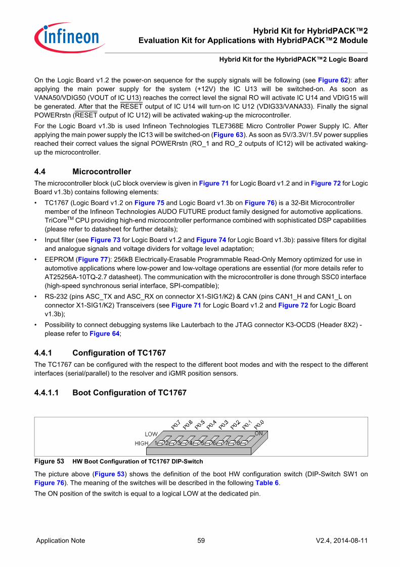
Hybrid Kit for HybridPACK™2Evaluation Kit for Applications with HybridPACK™2 Module
Hybrid Kit for the HybridPACK™2 Logic Board
Application Note 59 V2.4, 2014-08-11
On the Logic Board v1.2 the power-on sequence for the supply signals will be following (see Figure 62): afterapplying the main power supply for the system (+12V) the IC U13 will be switched-on. As soon asVANA50/VDIG50 (VOUT of IC U13) reaches the correct level the signal RO will activate IC U14 and VDIG15 willbe generated. After that the RESET output of IC U14 will turn-on IC U12 (VDIG33/VANA33). Finally the signalPOWERrstn (RESET output of IC U12) will be activated waking-up the microcontroller. For the Logic Board v1.3b is used Infineon Technologies TLE7368E Micro Controller Power Supply IC. Afterapplying the main power supply the IC13 will be switched-on (Figure 63). As soon as 5V/3.3V/1.5V power suppliesreached their correct values the signal POWERrstn (RO_1 and RO_2 outputs of IC12) will be activated waking-up the microcontroller.
4.4 MicrocontrollerThe microcontroller block (uC block overview is given in Figure 71 for Logic Board v1.2 and in Figure 72 for LogicBoard v1.3b) contains following elements:• TC1767 (Logic Board v1.2 on Figure 75 and Logic Board v1.3b on Figure 76) is a 32-Bit Microcontroller
member of the Infineon Technologies AUDO FUTURE product family designed for automotive applications. TriCoreTM CPU providing high-end microcontroller performance combined with sophisticated DSP capabilities (please refer to datasheet for further details);
• Input filter (see Figure 73 for Logic Board v1.2 and Figure 74 for Logic Board v1.3b): passive filters for digital and analogue signals and voltage dividers for voltage level adaptation;
• EEPROM (Figure 77): 256kB Electrically-Erasable Programmable Read-Only Memory optimized for use in automotive applications where low-power and low-voltage operations are essential (for more details refer to AT25256A-10TQ-2.7 datasheet). The communication with the microcontroller is done through SSC0 interface (high-speed synchronous serial interface, SPI-compatible);
• RS-232 (pins ASC_TX and ASC_RX on connector X1-SIG1/K2) & CAN (pins CAN1_H and CAN1_L on connector X1-SIG1/K2) Transceivers (see Figure 71 for Logic Board v1.2 and Figure 72 for Logic Board v1.3b);
• Possibility to connect debugging systems like Lauterbach to the JTAG connector K3-OCDS (Header 8X2) - please refer to Figure 64;
4.4.1 Configuration of TC1767The TC1767 can be configured with the respect to the different boot modes and with the respect to the differentinterfaces (serial/parallel) to the resolver and iGMR position sensors.
4.4.1.1 Boot Configuration of TC1767
Figure 53 HW Boot Configuration of TC1767 DIP-Switch
The picture above (Figure 53) shows the definition of the boot HW configuration switch (DIP-Switch SW1 onFigure 76). The meaning of the switches will be described in the following Table 6.The ON position of the switch is equal to a logical LOW at the dedicated pin.

Hybrid Kit for HybridPACK™2Evaluation Kit for Applications with HybridPACK™2 Module
Hybrid Kit for the HybridPACK™2 Logic Board
Application Note 60 V2.4, 2014-08-11
4.4.1.2 Selecting Serial/Parallel InterfaceDIP-4 switch (SW2 on Figure 72) is used to select serial/parallel interface for the communication with resolver oriGMR position sensor - please refer to Table 7.
Figure 54 The Boot Configuration Switch (SW1) and Serial/Parallel Interface Select Switch (SW2)
Table 6 User Startup Modes for TC1767
CFG[7...0] Type of Boot TC1767 11)
1) 1 to 8 are the DIP-Switch numbers (SW1 on Figure 54)
2 3 4 5 6 7 811XXX10X2)
2) The shadowed line indicates the default settings.
Internal Start from Flash OFF OFF X3)
3) ’x’ represents the don’t care state.
X X OFF ON X010XX100 Bootstrap Loader Mode, Generic Bootloader at
CAN pinsON OFF ON X X OFF ON ON
10101100 Bootstrap Loader Mode, ASC Bootloader OFF ON OFF ON OFF OFF ON ON10100100 Alternate Boot Mode, ASC Bootloader on fail OFF ON OFF ON ON OFF ON ON1011X10X Alternate Boot Mode, Generic Bootloader at
CAN pins on failOFF ON OFF OFF X OFF ON X
all others reserved; don’t use this combination
Table 7 Selecting Serial/Parallel Interface
SW2[4...1] Inetrface to the Resolver/iGMR 41)
1) 1 to 4 are the DIP-Switch numbers
3 2 100002)
2) 0 is equal to open switch, “1” is equal to closed switch
iGMR enabled (SPI and Incremental mode)Resolver in Parallel Mode
OFF3)
3) ’x’ represents the don’t care state.
OFF OFF OFF
1111 Resolver in Serial ModeiGMR disabled
ON ON ON ON
all others reserved; don’t use this combination

Hybrid Kit for HybridPACK™2Evaluation Kit for Applications with HybridPACK™2 Module
Hybrid Kit for the HybridPACK™2 Logic Board
Application Note 61 V2.4, 2014-08-11
4.5 WatchdogThe Logic Board contains a pin-selectable watchdog timer that supervises the microcontroller activity andsignalizes when the system is operating improperly. During normal operation, the microcontroller (GPTA39)should repeatedly toggle the watchdog input (WDI, see Figure 65) before the selected watchdog time-out periodelapses to report that the system is processing code properly. If this does not occurs, the supervisor asserts awatchdog output (WDO) which will reset the microcontroller via PORSTn (external power-on hardware reset).The state of the three logic control pins (SET0, SET1 and SET2) determines watchdog timing characteristics (seetable in Figure 65). The jumper J1 allows disabling the watchdog functionality in a very easy way.
4.6 Phase Current SensingPhase current sensing signals should be connected to the Logic Board connector X1-SIG1/K2 to the pins I_U, I_Vand I_W (Figure 73 for the Logic Board v1.2 and Figure 74 for the Logic Board v1.3b). The Logic Board isdesigned to work with current transducers (not provided with the Hybrid Kit) with voltage output proportional to thecurrent (usually deploying Hall effect - like LEM sensors). User can take +5V (analog) available on the X1-SIG1/K2pins to supply current transducers. The exact type of current transducer will be depend on many parameters inapplication, but usually the most important is the motor current consumption. Please notice that if you control 3-phase balanced synchronous system it is enough to measure just 2 phases, since the 3rd phase current can becalculated as algebraic combination out of the 2 measured currents.
4.7 Resolver InterfaceThe Logic Board includes a 12-Bit Resolver-to-digital converter (meaning A/D converter) which integrates an on-board programmable sinusoidal oscillator that provides sine wave excitation for resolvers (pins R1 and R2 onconnector X1-SIG1/K2). For more details please refer to the data sheet of the component (AD2S1200YST) andthe schematics of the circuit - for Logic Board v1.2 see Figure 66 and for Logic Board v1.3b see Figure 67. Withresistors (R155, R156, R157, R158, R159 and R160) user can trim the LMH6672 (dual op-amp) output voltagevalues (resolver excitation). On the Logic Board v1.3b is given additional possibility to trim the resolver excitationwith potentiometers (R483, R484, R485 - not populated, user should solder them if needed). Please refer to datasheet of used resolver to trim this values properly. The resolver response should be connected between pins S1and S3 (sine) and S2 and S6 (cosine) on the connector X1-SIG1/K2.
4.8 Encoder InterfaceIf encoder is used as a sensor for the motor position/speed sensing the following pins on connector X1-SIG1/K2should be connected: the phase A should be connected to pin PosA (Logic Board v1.2) or between pinsPosA/iGMR_A+ and PosA/iGMR_A- (Logic Board v1.3), the phase B should be connected to pin PosB (LogicBoard v1.2) or between pins PosB/iGMR_B+ and PosB/iGMR_B- (Logic Board v1.3b) and phase Z (index or zeromarker) should be connected to pin PosZ (Logic Board v1.2) or between pins PosZ/iGMR_Z+ and PosZ/iGMR_Z-(Logic Board v1.3b).
4.9 Hall Sensor InterfaceIf Hall sensor is used as a sensor for the motor position/speed sensing the following pins on connector X1-SIG1/K2should be connected: the phase U should be connected to pin PosU (Logic Board v1.2) or to pin PosU/iGMR_U(Logic Board v1.3b), the phase V should be connected to pin PosV (Logic Board v1.2) or to pin PosV/iGMR_V(Logic Board v1.3b) and phase W should be connected to pin PosW (Logic Board v1.2) or to pin PosW/iGMR_W(Logic Board v1.3b).

Hybrid Kit for HybridPACK™2Evaluation Kit for Applications with HybridPACK™2 Module
Hybrid Kit for the HybridPACK™2 Logic Board
Application Note 62 V2.4, 2014-08-11
4.10 GMR InterfaceAs mentioned on the beginning of the Chapter 4, the Logic Board v1.3b supports GMR interface by means of abi-directional SSC (SPI compatible), encoder (or incremental) and Hall sensor interface. It is explicitlyrecommended to use Infineon Technologies TLE5012 GMR-based angular sensor for rotor position sensing. TheTLE 5012 is a 360° angle sensor that detects the orientation of a magnetic field. This is achieved by measuringsine and cosine angle components with monolithic integrated Giant Magneto Resistance. For more details aboutTLE5012 please refer to the data sheets on Infineon Technologies internet pages.
Figure 55 GMR SSC Interface (Logic Board v1.3b only)
4.10.1 GMR SSC Interface ModeThe schematics of SSC interface on the Logic Board is shown on Figure 55. Signals on connector X1-SIG/K2 thatare used for SSC interface are: iGMR_CSn+/iGMR_CSn- (Chip Select, differential signals),iGMR_REn_DE+/iGMR_REn_DE- (Read Enable, differential signals), iGMR_DATA+/iGMR_DATA- (Serial Data,differential signals) and iGMR_CLK+/iGMR_CLK- (SSC Clock, differential signals) - all signals are listed inTable 5. On Figure 56 is presented the schematics of possible technical solution (implemented by InfineonTechnologies System Engineering) for usage of TLE5012. The PCB with TLE5012 and a few additionalcomponents is mounted perpendicular to the electric motor shaft - just as shown on Figure 57. The TLE5012 ison the opposite side of the PCB - next to the motor shaft.
I C 26 D S 92LV 010
D E1R E
5
D I N2
R O U T3 V
CC
8G
ND
4
D O/ R I +7
D O/ R I -6
I C 28 74LV C 2G 04GW
1A1
2A3
1Y6
2Y4
VC
C5
GN
D2
iGM R _D ATA +
iGM R _D ATA -
iG MR _ C S _uC
G N D _D I G1
G N D _D I G1
R 4 891K
G N D _ D I G1
R 4 901K
G N D _D I G1
V D I G33+ 3.3 V
iG MR _ R E _uC
iG MR _D I _uCiGM R _R O U T_uC R 447
100R
C 11 27
100n/ 16 V/ X7R
GN D _D I G 1
iG MR _R E n_D E +
iG MR _C S n+
iG MR _R E n_D E -
iG MR _C S n-
GN D _D IG 1
C 11 31
100n/ 16 V/ X7R
C 113010 p/1 6V/ X7 R
GN D _D I G1
GN D _D I G1
C 112810p/ 16V / X7R
V D I G33+ 3.3 V
iG MR _C LK +
iG MR _C LK -iG MR _ C LK _uC
iGM R _I N D EX _uC
R 4881K
VD I G33+3. 3V
GN D _D I G1
GN D _D I G1
C 1129
100n/ 16V / X7R
G N D _ D I G1
I C 32
D S90 LV03 1A
D ou t1+2
D i n11
Vcc
16G
ND
8
D out 1- 3
D ou t2+6
D out 2-5
D ou t3+ 10
D out 3-11
D ou t4+ 14
D out 4-13
D i n27
D i n39
D i n41 5
E N4
E N *1 2

Hybrid Kit for HybridPACK™2Evaluation Kit for Applications with HybridPACK™2 Module
Hybrid Kit for the HybridPACK™2 Logic Board
Application Note 63 V2.4, 2014-08-11
Figure 56 GMR SSC Interface - Proposal Using TLE5012
Figure 57 Picture of Possible Physical Implementation of the GMR Sensor
U4
AM26LS31C DR
1A1
1Y2
1Z3
G4
2Z 52Y6
2A7
GN D8
3A9
3Y10
3Z11
G12
4Z134Y14
4A15
VCC16
U1
D S90C 032BTM
R in1- 1
R in1+2
Rout 13
EN4
Rout 25 R in2+
6
R in2-7
GN D8
R in3-9
R in3+10
Rout 311
EN_n12
Rout 413 R in4+
14
R in4-15
VCC16
U 3
DS92LV010ATM
D E1
D in2
R out3
GND4
R E5
D O-6
D O+7
VCC8
U 2
TLE5012
C LK1
SC K2
CSQ3
DATA4
I FA5
VDD6
GND7
I FB8
R63k 30603
R 73k30603
R83k 30603
R93k 30603
R 103k30603
R113k 30603
R 554R 0603
R 41k0603
C1
100n
/16V
/X7R
/EM
K10
7B71
04K
A
0603
C2
10u
/10V
/X7
R/L
MK
316B
710
6KL
120
6
C3
100n
/16
V/X
7R
/EM
K1
07B
710
4KA
060
3
X15
H eader_7x2
1234567891011121314
C4
100
n/1
6V/X
7R/E
MK
107B
710
4K
A
0603
C5
100n
/16
V/X
7R
/EM
K1
07B
710
4KA
060
3
R3100R 0603
R2100R 0603
R1100R 0603
C6
10p
/25V
/X7R
060
3
C7
10p
/25
V/X
7R
0603

Hybrid Kit for HybridPACK™2Evaluation Kit for Applications with HybridPACK™2 Module
Hybrid Kit for the HybridPACK™2 Logic Board
Application Note 64 V2.4, 2014-08-11
4.10.2 GMR Encoder Interface ModeInfineon Technologies iGMR sensor TLE5012 can be used with encoder interface as well. This working mode isreferred as IIF Interface mode in theTLE5012 data sheet. To avoid signal integrity and EMC problems, withinHybrid Kit it is expected that the 2 phase signals (A and B) and zero (index) signal are provided differentially. Onthe connector X1_SIG (Figure 51) encoder inputs are: PosA/iGMR_A+ and PosA/iGMR_A (phase A),PosB/iGMR_B+ and PosB/iGMR_B (phase B) and PosZ/iGMR_Z and PosZ/iGMR_Z (phase Z - index) - pleaserefer to the Table 5. Please refer to the TLE5012 data sheet to get iGMR sensor running in incremental mode.
4.10.3 GMR Hall Sensor Interface ModeTLE5012 supports Hall sensor interface mode as well (iGMR emulates Hall sensor mode). For this purpose to theconnector X1-SIG/K2 inputs PosU/iGMR_U (phase U), PosV/iGMR_V (phase V) and PosW/iGMR_W (phase W)should be connected. Please notice (on Figure 74) that the pull-up resistors to 3.3V (R491, R492 and R493) arealready provided on the Logic Board. For more details on Hall sensor mode please refer to the TLE5012 datasheet.
4.11 Definition of Layers for the Logic BoardThe Logic Board was made keeping the following rules for the copper thickness and the space between differentlayers shown in Figure 58 for the Logic Board v1.2 (4 layers) and Figure 59 for the Logic Board v1.3b (6 layers).
Figure 58 Definition of the Layers for the Logic Board v1.2
Figure 59 Definition of the Layers for the Logic Board v1.3b
Copper Isolation
1: 35 µm / 1 oz.
2: 35 µm / 1 oz.
3: 35 µm / 1 oz.
4: 35 µm / 1 oz.
1-2: 0.5 mm
2-3: 0.5 mm
3-4: 0.5 mm
Copper Isolation
1: 35 µm
2: 35 µm
3: 35 µm
4: 35 µm
5: 35 µm
1
2
3
4
5
6
6: 35 µm
1
2
3
4
5
6
1-2: 0.5 mm 2-3: 0.5 mm 3-4: 0.5 mm 4-5: 0.5 mm 5-6: 0.5 mm
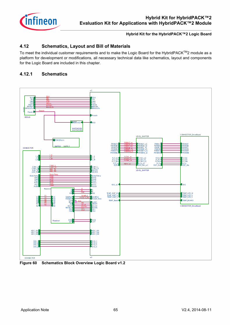
Hybrid Kit for HybridPACK™2Evaluation Kit for Applications with HybridPACK™2 Module
Hybrid Kit for the HybridPACK™2 Logic Board
Application Note 65 V2.4, 2014-08-11
4.12 Schematics, Layout and Bill of MaterialsTo meet the individual customer requirements and to make the Logic Board for the HybridPACKTM2 module as aplatform for development or modifications, all necessary technical data like schematics, layout and componentsfor the Logic Board are included in this chapter.
4.12.1 Schematics
Figure 60 Schematics Block Overview Logic Board v1.2
SUPPLYSUP PLY
POW ER rs t n
SC LK
OCDS
1
DEB UG
BR KIN nBR KOUTn
TRSTnTCK
TD I
R es et n
TD O
TMS
SO
LEV EL_SH IFTER
LEV EL_SH IFTER
FLTW n_uCFLTVn_uCFLTU n_uC
R ST_IN n_uC
PW MW T_uCPW MW B_uC
PW MVT_uCPW MVB _uC
PW MU T_uCPW MU B_uC
FLTU nFLTV nFLTW n
PWMW TPW MW B
PW MV TPWMVB
PWMU TPW MU B
R ST_I N nFLTn_uC FLTn
CON NEC TOR
CONN EC TOR
I _UI_V
I _W
PosUPos V
PosW
Pos Z
St at orTempPos APos B
S1
R1
S2
R2
S3
S6
A SC_RX
C AN1_LC AN1_HA SC_TX
AD C _I N1
D IO_1
AD C _I N2
D IO_2D IO_3D IO_4
AD C _I N3
R Dn
R es etn
PWMU T_ucPWMU B_ucPWMVT_uc
A
PWMVB_ucPWMW T_ucPWMW B_uc
B
C AN 1_L
SA MPLE
C AN 1_HASC _TXASC _RX
TMS
TD OTD I
TC KTR STnBR KIN n
S1S3
N M
R ESETn_resS2S6
R D VEL
R1R2
PosBPosASt at orTemp
PosZ
PosWPosVPosU
I _WI _VI _U
BR KOU Tn
RSTn_uc
Resolv er
R esolv er
S2S6
S3S1
R2R1
R ESETnC SnRD n
SC LKSO
RD VELn
BA
N M
FS1FS2
SAMPLE
D OSLOT
C ON N ECTOR_Driv erBoard
C ON N ECTOR_Driv erBoard
R ST_I Nn
PW MWTPW MWB
PW MVTPW MVB
PW MUTPW MUB
VD C
TEMP_BOAR D
FLTWnFLTVnFLTUn
FLTn
TEMP_H P2_UTEMP_H P2_W
TEMP_H P2_V
W ATCH D OGW ATCH D OG
W D O W D I
FS 2
uC
uC
TE MP_IGBT_UTEMP_I GBT_V
TE MP_IGBT_W
Pos UPos VPos W
BR KOUTn
TD ITMS
Pos Z
FLT_Wn
PW MU Tn
TC K
FLT_Vn
PW MVTnPW MUBn
FLT_Un
PWMW TnPW MVBn
TR STn
St atorTem p
PW MWBn
TD O
BR KI Nn
Pos A
R esetn
Pos B
R STn
I _UI _VI _W
FS 1
AS CTX
FS 2
AS CR X
SLS01MR ST1SC LK1
ABN M
SA MPLE
R D VEL
R esetn_R es
C AN 1_LC AN 1_H
AD C _I N1AD C _I N2
D I O_1D I O_2D I O_3D I O_4
D OSLOT
W D I
VD C_uC
F LT_n
TEMP_Board
AD C _I N3
FLTUn_uc
FS 1
FLTVn_ucFLTWn_uc

Hybrid Kit for HybridPACK™2Evaluation Kit for Applications with HybridPACK™2 Module
Hybrid Kit for the HybridPACK™2 Logic Board
Application Note 66 V2.4, 2014-08-11
Figure 61 Schematics Block Overview Logic Board v1.3b
P o s W / i GM R _ W
P o s V / i GM R _ V
P o s U / iG MR _ U
T E MP _ B O A R D
T E MP _ B O A R D
T e mp _ B o a rd
S U P P L Y
S U P P LY
P OW E R rs t n
A D 2 S 1 2 0 0_ D OS _ u CA D 2 S 1 2 0 0_ D OSA D 2 S 1 2 0 0_ L OT _ u CA D 2 S 1 2 0 0_ L OT
A D 2 S 1 2 0 0_ D B 11 _ S O
OC
DS
1
D E B U G
B R K I N nB R K O U T n
T R S T nTC K
TD I
R e se t n
T D O
TM S
A D 2 S 1 2 0 0_ D B 10 _ S C LKA D 2 S 1 2 0 0_ D B 9
A D 2 S 1 2 0 0_ S O E _ uC
A D 2 S 1 2 0 0_ D B 8A D 2 S 1 2 0 0_ D B 7A D 2 S 1 2 0 0_ D B 6
V D C _u C
A D 2 S 1 2 0 0_ D B 1 0_ S C L K _u C
S E R I A L _ P A R A L LE L_ M OD E _u C
A D 2 S 1 2 0 0_ D B 4A D 2 S 1 2 0 0_ D B 3
L E V E L_ S H I F T E R
L E V E L_ S H I F T E R
F L TW n_ u CF L TV n _ u CF L TU n _u C
R S T _ I N n _ u C
P W MW T_ u CP W MW B _ uC
P W MV T_ u CP W MV B _u C
P W MU T _u CP W MU B _ u C
F LT U nF L TV n
F L TW n
P W MW TP W MW B
P W MV TP W MV B
P W MU TP W M U B
R S T_ I N nF L Tn _ u C F L T n
A D 2 S 1 2 0 0_ D B 2A D 2 S 1 2 0 0_ D B 1A D 2 S 1 2 0 0_ D B 0
C O N N E C T OR
C ON N E C TO R
I _ UI _ V
I _ W
S t a t o rT e m p
S 1
R 1
S 2
R 2
S 3
S 6
A S C _ R X
C A N 1 _ LC A N 1 _ HA S C _ T X
A D C _ I N 1
D I O _ 1
A D C _ I N 2
D I O _ 2D I O _ 3
A D C _ I N 3
i GM R _ D A TA +
i GM R _ C LK +iG MR _ D A T A -
i GM R _ C S n -iG MR _ R E n _ D E +i G MR _R E n _ D E -
i GM R _ C S n +i GM R _ C L K -
P o s W / i GM R _ W
P os A / i G MR _A +P o s A / i GM R _ A -
P o sU / i GM R _ U
P os Z / i G MR _Z +
P o s V / i GM R _ V
P o s Z / i GM R _ Z -
P os B / i G MR _B +P o s B / i GM R _ B -
R e se t n
A D 2 S 1 2 0 0_ D B 5
P W M U T _ uc
A D 2 S 1 2 0 0_ F S 1 _ u C
P W M U B _ u cP W M V T_ u c
F L Tn _ u C
A
A D 2 S 1 20 0 _ D B 1 1 _ S O_ u C
P W M V B _ ucP W M W T _u cP W M W B _ uc
B
C A N 1 _L
A D 2 S 1 2 0 0_ S A M P L E n _u C
C A N 1 _HA S C _ T XA S C _ R X
T M S
T D OT D I
T C KT R S TnB R K I N n
S 1
A D 2 S 1 2 0 0_ D B 0 _u C
S 3 N M
A D 2 S 1 2 0 0_ R E S E T n _u C
S 2S 6
LE V E L_ S H I F T E R _ R E S OL V E R
LE V E L_ S H I F T E R _ R E S OL V E R
A D 2 S 1 2 0 0_ D B 0_ u C
A D 2 S 1 2 0 0_ D B 9_ u CA D 2 S 1 2 0 0_ D B 8_ u CA D 2 S 1 2 0 0_ D B 7_ u CA D 2 S 1 2 0 0_ D B 6_ u CA D 2 S 1 2 0 0_ D B 5_ u CA D 2 S 1 2 0 0_ D B 4_ u CA D 2 S 1 2 0 0_ D B 3_ u CA D 2 S 1 2 0 0_ D B 2_ u CA D 2 S 1 2 0 0_ D B 1_ u C
A D 2 S 1 2 0 0_ D B 0A D 2 S 1 2 0 0_ D B 1A D 2 S 1 2 0 0_ D B 2A D 2 S 1 2 0 0_ D B 3A D 2 S 1 2 0 0_ D B 4A D 2 S 1 2 0 0_ D B 5A D 2 S 1 2 0 0_ D B 6A D 2 S 1 2 0 0_ D B 7A D 2 S 1 2 0 0_ D B 8A D 2 S 1 2 0 0_ D B 9
A D 2 S 1 2 00 _ D B 11 _ S O_ u CA D 2 S 1 2 0 0_ D B 1 0_ S C L KA D 2 S 1 2 0 0_ D B 1 1_ S O
A D 2 S 1 2 00 _ D B 10 _ S C LK _ u C
A D 2S 12 0 0 _L O T_ u CA D 2 S 1 2 0 0_ D OS A D 2S 1 2 0 0 _D OS _ u CA D 2 S 1 2 0 0_ L OT
S E R I A L _ P A R A LL E L _ MO D E _ u CE N n
A D 2 S 1 2 0 0_ R D V E L n _ uC
R 1R 2
A D 2 S 1 2 0 0_ D B 1 _u C
S t a t or Te m p
B R K O U T n
A D 2 S 1 2 0 0_ D B 2 _u CA D 2 S 1 2 0 0_ D B 3 _u CA D 2 S 1 2 0 0_ D B 4 _u CA D 2 S 1 2 0 0_ D B 5 _u C
R S T n _ uc
A D 2 S 1 2 0 0_ D B 6 _u C
R es o l v e r
R es o l v e r
S 2S 6
S 3S 1
R 2R 1
BA
N M
A D 2 S 1 20 0 _ C S n
A D 2 S 1 20 0 _ D B 7A D 2 S 1 20 0 _ D B 8A D 2 S 1 20 0 _ D B 9
A D 2 S 1 20 0 _ D B 0A D 2 S 1 20 0 _ D B 1A D 2 S 1 20 0 _ D B 2A D 2 S 1 20 0 _ D B 3A D 2 S 1 20 0 _ D B 4A D 2 S 1 20 0 _ D B 5A D 2 S 1 20 0 _ D B 6
A D 2 S 1 20 0 _ D B 1 0 _ S C L KA D 2 S 12 0 0 _ D B 1 1 _ S O
A D 2 S 1 2 00 _ D OS
A D 2S 1 2 0 0 _R D V E Ln
A D 2 S 1 2 0 0_ L OT
A D 2 S 1 2 0 0_ F S 1A D 2 S 1 2 0 0_ F S 2
A D 2 S 1 20 0 _ R E S E TnA D 2 S 12 0 0 _ S A MP L E n
A D 2S 12 0 0 _S OE
A D 2 S 1 2 0 0_ D B 7 _u C
iG MR
i GM R
i G MR _D I _ uC
iG MR _ C L K _ uC
i GM R _ D A T A +
i GM R _ C L K +i GM R _ C L K -
i GM R _ D A T A -iG MR _ R O U T _ uC
i G MR _C S _ uCi G MR _R E _ uCi GM R _ C S n -
i GM R _ R E n _ D E +i GM R _ R E n _ D E -
i GM R _ C S n +
i GM R _ I N D E X _ uC
C ON N E C T OR _D r i v er B oa rd
C ON N E C T OR _D r i v er B oa rd
R S T _ I N n
P W MW TP W MW B
P W MV TP W MV B
P W MU TP W MU B
V D C
F LT W nF LT V nF LT U n
F LT n
T E M P _ H P 2 _ UT E M P _ H P 2 _ W
T E M P _ H P 2 _ V
A D 2 S 1 2 0 0_ D B 8 _u C
I _ W
A D 2 S 1 2 0 0_ D B 9 _u C
I _ VI _ U
W A TC H D OG
W A TC H D OG
W D O W D I
A D 2 S 1 2 0 0_ C S n_ u C
A D 2 S 1 2 0 0_ F S 2 _ u C
u C
u C
T E MP _I G B T _ UT E M P _ I GB T _ V
T E M P _ I GB T _ W
B R K OU T n
T D IT MS
F L T_ W n
P W MU Tn
T C K
F L T_ V n
P W MV TnP W M U B n
F LT _ U n
P W MW TnP W MV B n
T R S Tn
S t a t o rT e m p
P W MW B n
T D O
B R K I N n
R es e t n
R S Tn
I _ UI _ VI _ W
A S C T XA S C R X
ABN M
C A N 1 _ LC A N 1 _ H
A D C _ I N 1A D C _ I N 2
D I O_ 1D I O_ 2D I O_ 3
W D I
V D C _ u C
F L T _n
T E M P _ B oa rd
A D C _ I N 3
A D 2 S 1 20 0 _ D B 0 _ u C
A D 2 S 1 20 0 _ D B 9 _ u CA D 2 S 1 20 0 _ D B 8 _ u CA D 2 S 1 20 0 _ D B 7 _ u CA D 2 S 1 20 0 _ D B 6 _ u CA D 2 S 1 20 0 _ D B 5 _ u CA D 2 S 1 20 0 _ D B 4 _ u CA D 2 S 1 20 0 _ D B 3 _ u CA D 2 S 1 20 0 _ D B 2 _ u CA D 2 S 1 20 0 _ D B 1 _ u C
A D 2 S 1 20 0 _ LO T _u C
A D 2 S 1 20 0 _ R D V E L n_ u C
A D 2 S 1 20 0 _ D O S _ uC
A D 2 S 1 20 0 _ F S 2 _u CA D 2 S 1 20 0 _ F S 1 _u C
A D 2 S 1 20 0 _ D B 1 1 _ S O_ u CA D 2 S 1 20 0 _ D B 1 0 _ S C L K _ u C
A D 2 S 1 20 0 _ C S n _ u C
A D 2 S 1 20 0 _ R E S E Tn _ u CA D 2 S 1 20 0 _ S A MP LE _ u C
S E R I A L _ P A R A LL E L _ MO D E _ u C
i GM R _ D I _ uC
i GM R _ C LK _u Ci GM R _ R OU T_ u C
i GM R _ C S _ uCi GM R _ R E _ uC
P o s W / i GM R _ W
P o s A / i GM R _ A +P o s A / i GM R _ A -
P o s U / i G MR _U
P o s Z / i GM R _ Z +
P o s V / i GM R _ V
P o s Z / i GM R _ Z -
P o s B / i GM R _ B +P o s B / i GM R _ B -
A D 2 S 1 20 0 _ S OE _ u C
i GM R _ I N D E X _ u C
F L TU n _u cF L TV n_ u c
P o s B / i GM R _ B -P o s B / i GM R _ B +P o s A / i GM R _ A -P o s A / i GM R _ A +
P o s Z / i GM R _ Z -P o s Z / i GM R _ Z +
F L TW n_ u c
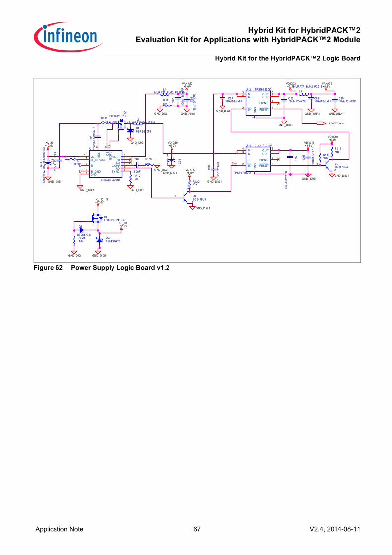
Hybrid Kit for HybridPACK™2Evaluation Kit for Applications with HybridPACK™2 Module
Hybrid Kit for the HybridPACK™2 Logic Board
Application Note 67 V2.4, 2014-08-11
Figure 62 Power Supply Logic Board v1.2
C 9010uf / 10V/X7R
Q4IP D90P03P4L-04
GND _D IG1
C98
100n
/16V
/X7R
0.4A / 1.4W
C97
10uF
/6.3
V/X7
R
VDI G15+1. 5V
GND _DI G1
C95
100n
/16V
/X7R
KL_30_I N+12. 0V
R11447mR /0.33W
R119680R
GND _D IG1
GND _D IG1
D1MBR S340T3
GND _D IG1
GN D_DI G1
R 1130R
C92
220n
F/50
V/X7
R
KL_30+12. 0V
L347uH /B82464G4473M
R 11810K
Q1SPD09P06PLG
U13
TLE6389-2GV50
SI _EN ABLE1 FB 2VOUT 3
GND4 SY NC 5SI _GND6SI7 C OMP 8SO 9
RO 10
BDS
11
GDR
V12
VS13 CS
14
+
C94
100u
F/10
V
R1210R
L1MUR ATA_BLM21P221SN
GN D_ANA1
GN D_DI G1
VAN A50+5.0V
C85
100n
/16V
/X7R
+
C93
100u
F/35
V/M
AL21
4095
001E
3
GN D_DI G1
GN D_DI G1C8
622
u/16
V/X7
R
C96
2. 2nF
C91
220n
F/50
V/X7
R
KL_30+12.0V
R11610K
R 12810K
GN D_DI G1GND _D IG1
R 11510K
ENn
POWER rs tn
Q3BC 847BL3
1
3
2
R12210K
GND _D IG1
U 12 TPS76733QD
GND
1
EN2
IN3IN4 OU T 5
OU T 6
FB/ N C 7
RES ET 8
C87100n/16V/ X7R
U 14
TPS76715QD
GND
1
EN2
IN3 IN4 OU T 6
OU T 5
FB/ N C 7
RES ET 8
GN D_DI G1
C 8810uf / 10V/X7R
GN D_D IG1
GND _ANA1 GN D _AN A1
VANA33+3.3V
VD IG33+3. 3V
Q2BC 847BL3
1
3
2
VD I G50+5. 0V
L2MUR ATA_BLM21P221SN
C89100n/16V/ X7R
D2
BZV55/C 13
VD IG50+5.0V
VDI G50+5. 0V
GND _D IG1
D 31SMB30AT3
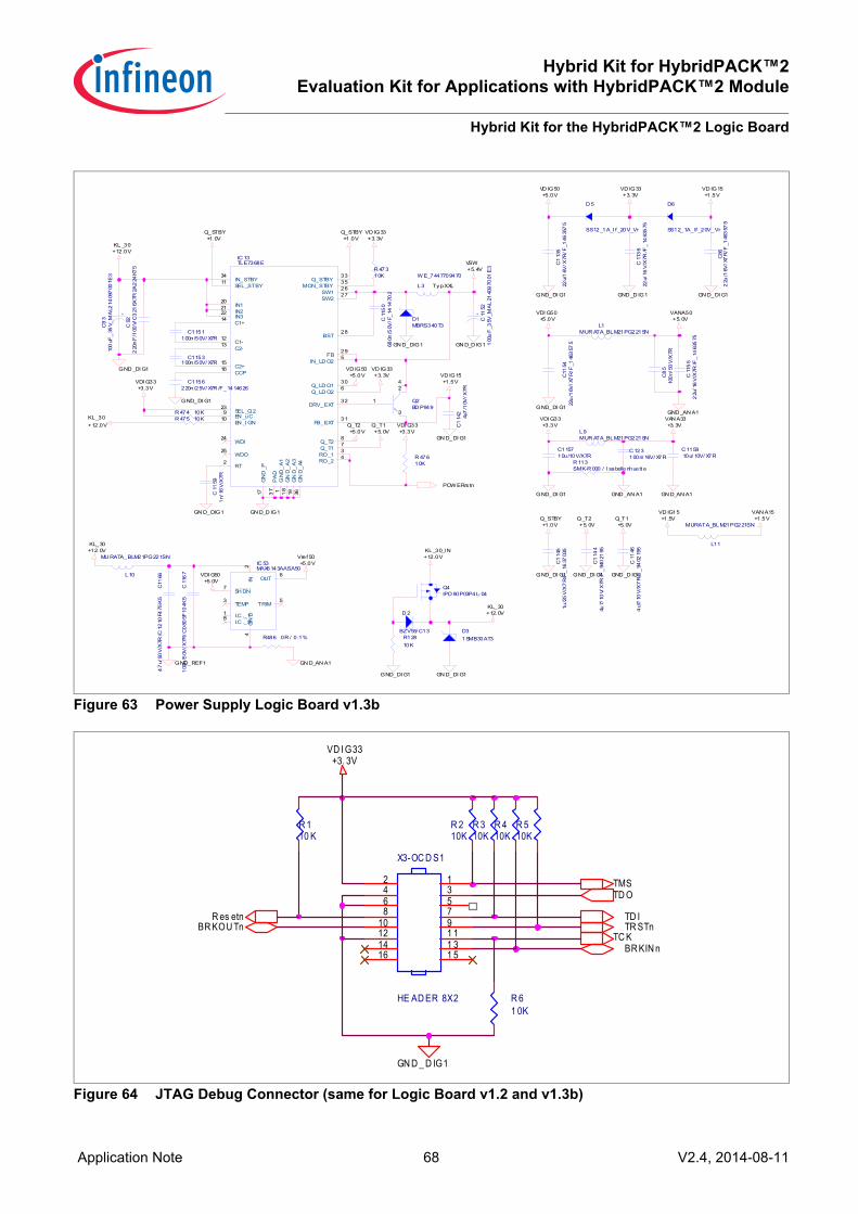
Hybrid Kit for HybridPACK™2Evaluation Kit for Applications with HybridPACK™2 Module
Hybrid Kit for the HybridPACK™2 Logic Board
Application Note 68 V2.4, 2014-08-11
Figure 63 Power Supply Logic Board v1.3b
Figure 64 JTAG Debug Connector (same for Logic Board v1.2 and v1.3b)
Q4IPD 90P03P4L-04
L11
MURATA_BLM21PG221SN
VD IG15+1.5V
VAN A15+1.5V
KL_30_I N+12.0V
KL_30+12. 0V
+
C11
521
00u
F_3
5V_M
AL
2140
970
01E
3
R12810K
GND_DI G1
C11
5422
u/1
6V/X
7R
/F_1
463
575
C11
55
22u
/16
V/X
7R/F
_14
635
75
GN D_DI G1
C11
664.
7u/
50V
/X7R
/C12
10F4
75K
5
+
C9
310
0uF
_35
V_M
AL2
1409
700
1E3
R 474 10K
VDI G50+5.0V
GND _DI G1GND_DI G1
C 115810u/ 10V/ X7R
GND _D IG1
C86
22u
/16V
/X7
R/F
_146
357
5
Q_T1+5. 0V
Q_T2+5. 0V
Q_T1+5. 0V
VD IG15+1.5V
C1151100n/50V/ X7R
C1153100n/50V/ X7R
Q_T2+5.0V
VDI G33+3.3V
GND_DI G1
Q_STBY+1. 0V
C1156220n/25V/ X7R /F_1414626
R 47610K
VD IG33+3. 3V
VDI G50+5.0V
VD IG33+3. 3V
C11
464
u7/1
0V
/X7
R/F
_94
0219
5
R 47310K
Q_STBY+1.0V
VSW+5. 4V
Q_STBY+1.0V
D1MBRS340T3
GN D_D IG1
GND _DI G1 VD IG50+5.0V
R 113SMK-R 000 / I sabellenhuett e
POW ERrs tn
C1
145
1u/2
5V
/X7
R/F
_16
3703
5
KL_30+12.0V
IC 13TLE7368E
GN
D_
A1
1
RT2
RO_13
RO_24
IN_LD O25
Q_LD O26
Q_T17Q_T28
EN _uC9
EN _I GN10
SEL_STBY11
C1-12
C2-13
C1+14
C2+15
CCP16
GN
D_P
17
GN
D_
A2
18
GN
D_
A3
19
IN120
IN221
IN322
SEL_Q223
WDI24
WDO25
SW126
SW227
BST28
FB29
Q_LD O130
FB_EXT31
DRV_EXT32
Q_STBY33
IN_STBY34
MON_STBY35
GN
D_
A436
PA
D3
7
KL_30+12.0V
L3
W E_7447709470
Ty p XXL
C92
220
nF
/100
V/C
321
6X7R
2A2
24KT
5
D 5
SS12_1A_I f _20V_Vr
VD IG15+1.5V
C11
591
n/16
V/X
7R
VD IG33+3. 3V
VD IG50+5.0V
GN D_DI G1
IC 53MAX6143AASA50
I.C ._11
IN2
TEMP3
GN
D4
TRIM5
OUT6
SH DN7
I.C ._88
GND_DI G1
C1
142
4u7
/10V
/X7R
GND_DI G1
GN D_DIG1
GN D_DI G1
C115710u/10V/X7R
VDI G33+3.3V
C11
67
100
n/5
0V/X
7R/C
080
5F10
4K5
GND _AN A1
GND_DI G1
GN D_AN A1
GND _D IG1
D6
SS12_1A_If _20V_Vr
R486 0R / 0.1%
R 475 10K
C1
135
22u/
16V
/X7R
/F_1
4635
75
GND_REF1
Vref 50+5.0V
GN D_AN A1
VDI G33+3.3V
VAN A33+3. 3V
L1MUR ATA_BLM21PG221SN
GND _AN A1
VANA50+5. 0V
C8
510
0n/
50V
/X7R
GN D_DIG1
C1
144
4u7/
10V/
X7R
/F_
940
2195
Q2BD P949
1
2
3
4
L9MUR ATA_BLM21PG221SN
C 123100n/ 16V/ X7R
C11
50
680n
/50V
/F_
1414
702
KL_30+12. 0V
GN D_D IG1
C11
36
22u/
16V
/X7R
/F_
1463
575
D 2
BZV55/ C13
L10
MU RATA_BLM21PG221SN
D31SMB30AT3
BR KOU TnTC K
BR KIN n
R es etn TD I
VD I G33+3. 3V
GN D _ D IG1
R 210K
R 310K
R 410K
R 110 K
R 61 0K
R 510K
TR STn
TD OTMS
X3-OC D S1
HE AD ER 8X2
2468
10121416
135791 11 31 5
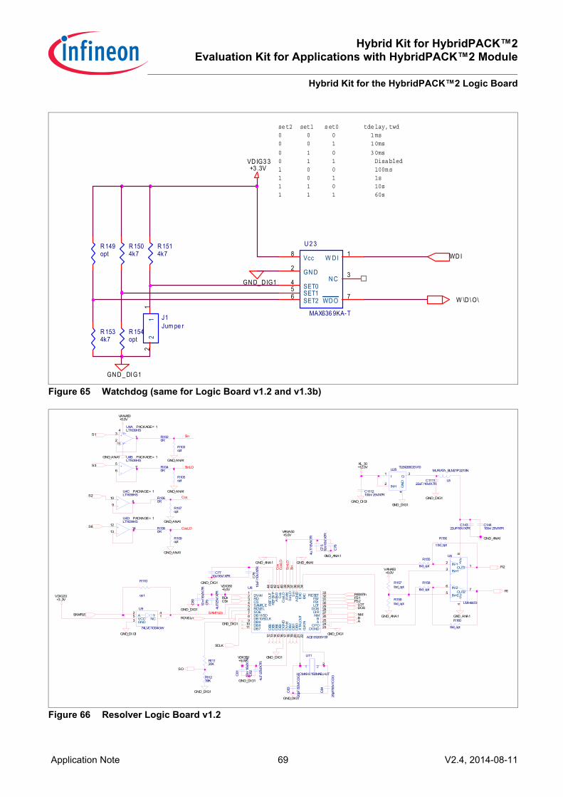
Hybrid Kit for HybridPACK™2Evaluation Kit for Applications with HybridPACK™2 Module
Hybrid Kit for the HybridPACK™2 Logic Board
Application Note 69 V2.4, 2014-08-11
Figure 65 Watchdog (same for Logic Board v1.2 and v1.3b)
Figure 66 Resolver Logic Board v1.2
U 2 3
MAX636 9KA-T
W D I 1
GN D2N C 3
SET04SET15
SET26 WD O 7
Vcc8
W \D \ O\
WD I
GN D_ D IG1
J1Jum pe r
11
22
R 1514k7
R 1504k7
R 149opt
R 1534k7
R 154opt
GN D _ DI G1
set2 set1 set0 tdelay,twd0 0 0 1ms 0 0 1 10ms
0 1 0 30ms 0 1 1 Disabled 1 0 0 100ms 1 0 1 1s 1 1 0 10s 1 1 1 60s
VD IG3 3+3 .3V
GND_DI G1
R1040R
R105opt
GND_ANA1 C1112100n/ 25V/X7R
GND_DI G1
VDIG33+3.3V
R107opt
R1060R
GND_ANA1
R109opt
R1080R
GND_ANA1
L8
MURATA_BLM21P221SN
C81
10n/
16V/
X7R
C78
10uF
/10V
/X7R
U11
HCM49 8.192MABJ-UT
11
22
C84
20pF
/50V
/CO
G
C79
4u7/
25V/
X7R
C75
4u7/
16V/
X7R
C80
10n/
16V/
X7R
C76
10n/
16V/
X7R
C82
4u7
/25V
/X7R
C83
20pF
/50V
/CO
G
C7710n/16V/ X7R
RDnCSn
RESETn
GND_DIG1
ABRDVELn
SCLK
FS2FS1
NM
R11239K
R11120K
SO
C111122uF/16V/X7R
GND_DIG1
R1
R2
R156
t bd_opt
R155
tbd_opt
R159tbd_opt
R157tbd_opt
R160
tbd_opt
R158
tbd_opt
GND_DIG1
LOT
VANA50+5.0V
DOS
S3
VDIG50+5.0V
VDIG50+5.0V
Sin
SinLO
Cos
+
-
V+
V-
U4ALT1639HS
PACKAGE = 1
3
21
4
11
CosLO
+
-
U4BLT1639HS
PACKAGE = 1
5
67
+
-
U4CLT1639HS
PACKAGE = 1
10
98
VANA50+5.0V
GND_ANA1
+
-
U4DLT1639HS
PACKAGE = 1
12
1314
VANA50+5.0V
GND_ANA1
GND_ANA1
U9
74LVC1G04GW
NC1A
2
GND3Y
4
VCC5
GND_ANA1
Sin
GND_ANA1
Sin
LO
S1
U8
AD2S1200YST
DVdd1
RD2
CS3
SAMPLE4
RDVEL5
SOE6
DB11/SO7
DB10/SCLK8
DB99DB810DB711 D
B612
DB5
13D
B414
DB3
15D
GN
D16
DV
dd17
DB
218
DB
119
DB
020
XTA
LOUT
21
CLK
IN22
DGND 23CPO 24A 25B26NM27DI R28DOS29LOT30FS131FS232RESET33
EXC
34E
XC35
AG
ND
36S
in37
Sin
LO38
AVd
d39
Cos
LO40
Cos
41A
GND
42R
EFBY
P43
REF
OUT
44
GND_DIG1
Cos
LO
GND_DIG1
C14322uF/16V/X7R
C144100n/ 25V/X7R
GND_DI G1
U6
LMH6672
OUT1 1IN-12
IN+13
-Vs
4
IN+25
IN-26
OUT27
+Vs
8
GND_DIG1
S2
S6
Cos
GND_DIG1
GND_DIG1
GND_DIG1
GND_ANA1
R110
opt
KL_30+12.0V
U25TLE4266GSV10
I1
INH2
Q3
GN
D4
R1020R
SAMPLEn
GND_ANA1
R103opt
GND_ANA1
SAMPLE

Hybrid Kit for HybridPACK™2Evaluation Kit for Applications with HybridPACK™2 Module
Hybrid Kit for the HybridPACK™2 Logic Board
Application Note 70 V2.4, 2014-08-11
Figure 67 Resolver Logic Board v1.3b
Figure 68 Level Shifter for Adapting 3.3V to 5V Logic Levels Logic Board v1.2
C1216opt
GND_ANA1
IC30
74LVC2G04GW
1A1
2A3
1Y6
2Y4
VC
C5
GN
D2
GND_ANA1
C1217opt
R1040R
R105opt
GND_ANA1
GND_DIG1
R1060R
R107opt
GND_ANA1
TP1Testpad_SMD_Ettinger
R1080R
R109opt
GND_ANA1
L8
MURATA_BLM21PG221SN
TP2Testpad_SMD_Ettinger
C8
1
10n/
16V
/X7R
C7
8
10uF
/10V
/X7R
U1
HCM49 8.192MABJ-UT
11
22
C8
4
20pF
/50V
/CO
G
C7
9
4u7/
25V
/X7R
C7
5
4u7/
16V
/X7R
C8
0
10n/
16V
/X7R
AD
2S12
00_
DB
6
C7
6
10n/
16V
/X7R
C8
2
4u7/
25V
/X7R
TP3Testpad_SMD_Ettinger
C8
3
20pF
/50V
/CO
G
C7
7
10n/
16V
/X7R
AD2S1200_CSn
AD2S1200_RESETn
GND_DIG1
AB
AD2S1200_RDVELn
AD2S1200_FS2AD2S1200_FS1
NM
TP4Testpad_SMD_Ettinger
TP5Testpad_SMD_Ettinger
AD2S1200_DB11_SO
C111122uF/16V/X7R
TP6Testpad_SMD_Ettinger
R1
R2
R155
2K4/0.1%
R156
2K4/0.1%
R1593K3/0.1%
R157390/0.1%
R160
2K4/0.1%
R158
2K4/0.1%
TP7Testpad_SMD_Ettinger
GND_DIG1
TP8Testpad_SMD_Ettinger
AD2S1200_LOT
VANA50+5.0V
AD2S1200_DOS
AD
2S12
00_
DB
5
C1163
100n/16V/X7R
AD
2S12
00_
DB
4
TP9
Testpad_SMD_
AD
2S12
00_
DB
3
S3
AD
2S12
00_
DB
2
VDIG50+5.0V
AD
2S12
00_
DB
1
GND_ANA1
AD
2S12
00_
DB
0
VDIG50+5.0V
Sin
SinLO
Cos
+
-
V+
V-
IC4ALT1639HS
PACKAGE = 1
3
21
4
11
CosLO
+
-
IC4BLT1639HS
PACKAGE = 1
5
67
+
-
IC4CLT1639HS
PACKAGE = 1
10
98
VANA50+5.0V
GND_ANA1
+
-
IC4DLT1639HS
PACKAGE = 1
12
1314
VANA50+5.0V
GND_ANA1
GND_ANA1
Sin
GND_ANA1
AD2S1200_DB9AD2S1200_DB8
Sin
LO
AD2S1200_DB7
S1
IC8
AD2S1200YST
DVdd1
RD2
CS3
SAMPLE4
RDVEL5
SOE6
DB11/SO7
DB10/SCLK8
DB99
DB810
DB711
DB
612
DB
513
DB
414
DB
315
DG
ND
16
DV
dd17
DB
218
DB
119
DB
020
XT
ALO
UT
21
CL
KIN
22
DGND23CPO24A25B26NM27DIR28DOS29LOT30FS131FS232RESET33
EX
C34
EX
C35
AG
ND
36S
in37
Sin
LO38
AV
dd39
Co
sLO
40C
os
41A
GN
D42
RE
FBY
P43
RE
FOU
T44
C1164
100n/16V/X7R
GN
D_
DIG
1
R47110K
AD2S1200_SOE
GND_DIG1
Co
sLO
GND_DIG1
C14322uF/16V/X7R
C144100n/25V/X7R
GND_DIG1
IC6
LMH6672
OUT11IN-1
2
IN+13
-Vs
4
IN+25
IN-26
OUT27
+Vs
8
GND_DIG1
S2
S6C
os
GND_DIG1
GND_ANA1
VDIG33+3.3V
GND_DIG1
R110
opt
AD2S1200_SAMPLEn
C1
112
100n
/50V
/X7R
/C0
805
F10
4K5
GND_ANA1
R4855K_pot_0,25W_20%_Bourns_3314J_opt
R4
845K
_po
t_0
,25W
_20%
_B
ourn
s_33
14J_
opt
KL_30+12.0V
R4835K_pot_0,25W_20%_Bourns_3314J_opt
AD2S1200_DB10_SCLK
IC25TLE4266GSV10
I1
INH2
Q3
GN
D4R102
0R
GND_ANA1
R103opt
GND_ANA1
GND _DI G1
FLTn_uC
R951K
C 68100n/16V/X7R
R9315K
GND _DI G1
GN D_D IG1
C71100n/16V/ X7R
R1001K
VDI G50+5.0V
R9915K
FLTn
GND _DI G1
VDI G50+5. 0V
GN D_D IG1
GN D_D IG1
GN D_DIG1
C 70100n/16V/X7R
R981K
GND _DI G1
R9615K VDIG50+5. 0V
C60100pF/ 50V/ COG
R72100R
GND _DI G1
C61100pF/ 50V/ COG
R87100R
GND _DI G1
C62100pF/ 50V/ COG
GND _DI G1
R89100R
C63100pF/ 50V/ COG
R91100R
GND _DI G1
C67100pF/ 50V/ COG
GND _DI G1
R94100R
C69100pF/ 50V/ COG
GND _DI G1
R97100R
PWMW B
PWMWT
PWMUT
PWMVB
PWMVT
PWMU B
R9015K
R921K
C64100n/16V/X7R
VDI G50+5.0V
GND _DI G1VD IG50+5.0V
VDI G50+5. 0V
R84
1K
R82
1K
R7
91K
R80
1K
C 66100n/16V/X7R
R73 10K
R76
1K
R71 10K
R8
51K
R83
1K
C 65100n/16V/X7R
R8
11K
VDI G33+3.3V
R78
1K
R7
41
K
R8
81
K
R77
1K
U2
74ALVC 164245DGG
VCCA31
1D IR1
1A047
1A146
1A244
1A343
1A441
1A540
1A638
1A737
GN D4
GN D10
VCC B18VCC B7
1OE48
1B02
1B13
1B25
1B3 6
1B48
1B59
1B611
1B712
GN D15
2A036
2A135
2A233
2A332
2A430
2A529
2A627
2A726
2B013
2B114
2B216
2B3 17
2B419
2B520
2B622
2B723
2D IR24
2OE25
GN D21
GND28
GND 34
GND39
GND45
VCCA42
R7
51K
R8
61K
FLTU n_uCFLTVn_uCFLTWn_uC
PWMWB_uCPW MWT_uC
RST_INn_uC
PW MUT_uCPW MVB_uCPWMVT_uC
PWMUB_uC
FLTWn
FLTVn
FLTUn
R ST_I Nn

Hybrid Kit for HybridPACK™2Evaluation Kit for Applications with HybridPACK™2 Module
Hybrid Kit for the HybridPACK™2 Logic Board
Application Note 71 V2.4, 2014-08-11
Figure 69 Level Shifter for Adapting 3.3V to 5V Logic Levels Logic Board v1.3b
Figure 70 Connector to the Driver Board (same for Logic Board v1.2 and v1.3b)
GND_DI G1
FLTn_uC
R951K
R9315K
GND_DI G1
C68100n/16V/ X7R
VD IG50+5. 0V
GND_DI G1
R1001K
C71100n/ 16V/ X7R
R9915K
GND _DI G1
FLTn
VDI G50+5. 0V
GND _D IG1
GN D_DIG1
GND _D IG1
GND_DI G1
C70100n/16V/ X7R
R981K
R9615K VD IG50
+5.0V
R921K
R9015K VD IG50+5. 0V
GND_DI G1
C 64100n/16V/ X7R
VDI G50+5. 0V
VDI G50+5. 0V
R7
91K
R80
1K
R 73 10K
C66100n/16V/X7R
R7
110
K
R76
1K
C65100n/16V/ X7R
VDIG33+3. 3V
R7
81K R
881
K
R74
1K
R7
71K
R75
1K
I C2
74ALVC164245DGG
VC CA31
1DIR1
1A047
1A146
1A244
1A343
1A441
1A540
1A638
1A737
GND4
GND10
VCCB18VCCB7
1OE48
1B02
1B13
1B25
1B36
1B48
1B59
1B611
1B7 12
GND15
2A036
2A135
2A233
2A332
2A430
2A529
2A627
2A726
2B013
2B114
2B216
2B317
2B419
2B5 20
2B622
2B723
2DI R24
2OE25
GND21
GND28
GND 34
GND39
GND45
VC CA42
FLTUn_uCFLTVn_uCFLTWn_uC
PWMU T_uCPWMVB_uCPWMVT_uC
PW MWB_uCPWMW T_uC
RST_IN n_uC
FLTW n
FLTVn
FLTU n
PW MUB_uCRST_IN n
PWMVT
PWMWB
PWMW T
PWMUB
PWMU T
PWMVB
A D 2S 1200_D B 11_SO_uC
A D2S1200_D B0
I C 29
74LVC H 16T245D L
VC C A31
1D IR1
1A047
1A1461A244
1A3431A441
1A5401A638
1A737
GN D4
GN D10
VC C B18VC C B 7
1OE48
1B0 2
1B1 31B2 5
1B3 61B4 8
1B5 91B6 11
1B7 12
GN D15
2A0362A135
2A233
2A332
2A430
2A529
2A627
2A726
2B0 132B1 14
2B216
2B3 17
2B419
2B5 20
2B622
2B7 23
2DI R 242OE 25
GN D21
GN D 28
GN D34
GN D 39
GN D45
VC C A42
A D2S1200_D B1
GN D _DI G1
GND _D I G1
A D2S1200_D B2
GN D _D I G1
A D2S1200_D B3
A D2S1200_D B10_SC LK
A D2S1200_D B4
VD IG50+5.0V
A D2S1200_D B5A D2S1200_D B6
C 1133100n/ 16V /X7R
VD IG33+3. 3V
C 1132100n/16V/ X7R
A D2S1200_D B7
A D 2S 1200_D B 0_uC
A D2S1200_D B8
A D2S 1200_D B10_SC LK_uC
A D 2S 1200_D B 1_uC
A D2S1200_D B9
A D 2S 1200_D B 2_uCA D 2S 1200_D B 3_uC
A D2S1200_D B11_SO
SER I AL_PAR ALLEL_MOD E_uC
A D 2S 1200_D B 4_uC
A D2S1200_D OS
A D 2S 1200_D B 5_uC
A D2S1200_LOT
A D 2S 1200_D B 6_uCA D 2S 1200_D B 7_uCA D 2S 1200_D B 8_uCA D 2S 1200_D B 9_uC
A D 2S 1200_D OS_uCA D 2S 1200_LOT_uC
EN n
R 498 0R _opt
R 497 0R
GND _D I G1
R 456 1K
K1
TW-12-06-L-D-475-SM-A
11
22
33 4 4
55 6 6
77
88
99
1010
1111
1212
1313 14 14
1515
1616
1717
1818
1919
2020
2121 22 22
2323 24 24
PWMWTRST_INn
PWMVBPWMVTPWMWB
PWMUBPWMUT
VDC
FLTVn
FLTWnTEMP_BOAR D
FLTnFLTU n
VANA50_D B
TEMP_HP2_V
TEMP_HP2_W
TEMP_HP2_U
KL_30+12. 0V
GND _DIG1
KL_30+12.0V
GN D_D IG1GN D_ANA1

Hybrid Kit for HybridPACK™2Evaluation Kit for Applications with HybridPACK™2 Module
Hybrid Kit for the HybridPACK™2 Logic Board
Application Note 72 V2.4, 2014-08-11
Figure 71 Microcontroller Logic Board v1.2
C10
7
100n
/16V
/X7
R
F LT _ V n
V D I G3 3+ 3. 3 V
GN D _ D I G 1
GN D _ D I G1
V D I G5 0+ 5 . 0V
G N D _D I G1
D O S
F LT _ W nF L T _ W n
F L T _ U n
T E M P _ B o ard
P o s BP o s A
P o s Z
C11
2
100
n/1
6V/X
7R
TM STD O
TC KTD I
B R K O U T nB R K I N n
T R S T n
T MST D O
T C KT D I
B R K O U T nB R K I N n
T R S Tn C10
6
100
n/1
6V/X
7RC
104
10n
/16V
/X7R
GN D _ D I G 1
U 1 6E H 2 64 5 E T T TS - 20 . 0 0 0M
T R I1
GN D2
O U T3
V D C4
L 5M U R A T A _ B L M2 1 P 22 1 S N
V D I G 33+ 3 . 3 V
R 13 35 k 1
C10
5
22uF
/6.3
V/X
7R
R es e t n
R D V E L
C 1 1 3
10 0 n / 16 V / X 7 R
I N P U T _ F I L TE R
I n p ut _ F i l t e r
P o s AP o s BP o s Z
G P TA 12G P TA 38
G P TA 46
P o s WP o s VP o s U
G P TA 44G P TA 42
G P TA 14ABN M
G P TA 24
D I O_ 1D I O_ 2D I O_ 3D I O_ 4
G P TA 17
G P TA 21
S t a t o rT e mp
V D C
T E M P _I GB T _ UT E M P _I GB T _ VT E M P _I GB T _ W
I _ UI _ VI _ W
A N 15A N 14
A N 3
A N 4
A N 1A N 6
A D C _ I N 1 A N 16A D C _ I N 2 A N 17
A N 19
G P TA 32
A N 2
A N 13
G P TA 11
G P TA 43
G P TA 45
T E M P _B oa rd A N 12
A D C _ I N 3
A N 31
F L T _ V n
R e s et n
C 11 1
1 0 0n / 1 6 V / X 7R
MR S T 1
GN D _ D I G1
W D I
R 1 3 4
1K
P os VP o s U
P os W
P W MU B nP W MU T n
P W MV B n
P W MV T n
P W MW B n
P W MW T n
R 13 51K
S t a t or Te m p
EEP
ROM
E E P R OM
CSn
SCK SI SO
C1
15
100
n/1
6V/X
7R
C1
14
100n
/16V
/X7
R
R e s e t n_ R es
V D I G 33+ 3. 3 V
R X D O A
T X D O A
U 1 8M A X 32 3 2 E I P W R Q1
C 2+4
C 1+1
C 1-3
T2 o u t7
V - 6
T 2 in1 0
R 2 i n 8
T 1 in1 1
R 1o u t1 2
R 1 i n1 3
R 2o u t9
V +2
C 2-5
V c c1 6
G N D1 5
T1 o u t1 4
GN D _ D I G 1
G N D _ D I G1
G N D _D I G1G N D _ D I G 1
A S C R X
A S C T X
S C L K 1
S L S 0 1
I _ UR 3 15 0 R _ o p t
F LT _ n
C108
22u
F/6.
3V/
X7R
D I O _1
R 13 16 0 R
R 13 26 0 R
C 1 1 04 . 7 n/ 5 0 V / X 7 R
G N D _ D I G 1
F L 1
B 8 27 8 9 C 0 1 04 N 00 1
1
2 3
4
D I O _2
I _ V
D I O _3D I O _4
I _ W
F L T _ n
R 3 16 0 R
V D C _ u C
T E M P _ I GB T _ U
T E M P _ I GB T _ WT E M P _ I GB T _ V
A D C _I N 1
F S 1
A
R S T n
C A N 1_ H
u c _ T C 1 7 67
u c _ T C 1 7 67
A N 1 4A N 1 5
GP T A 3 8GP T A 1 2
GP T A 2 6
GP T A 2 7
GP T A 1 9
GP T A 1 8GP T A 2 0
GP T A 1 3
GP T A 1 4
GP T A 1 5GP T A 9GP T A 8
A N 1
TD OTM S
TD ITC KTR S T n
B R K I N nB R K O U T n
C l k
T XD 0 AR XD 0 A
S LS O0
S LS O1
S C L K 0
M TS R 0M R S T 0
P OR S T n
A N 6
GP T A 3 4GP T A 3 5
S C L K 1M R S T 1
GP T A 2 4
GP T A 1 0
GP T A 4 2GP T A 4 4GP T A 4 6
GP T A 4 0
GP T A 4 1
R X D C A N 1T X D C A N 1
A N 1 6A N 1 7A N 1 9
A N 3
A N 4
GP T A 2 1
GP T A 1 7GP T A 3 2
A N 2
P 5_ 8P 5_ 9
A N 1 3
GP T A 3 9
GP T A 1 1
GP T A 4 3
GP T A 4 5
A N 1 2
GP T A 2 8
A N 3 1 GP T A 2 9GP T A 3
A D C _I N 2
F S 2
R 1 0 11 0K
V D I G 3 3+ 3 . 3 V
A D C _I N 3
B
C A N 1_ L
F LT _ U n
L OT
N M
C A N _ T X 1
U 17T L E 6 25 0 GV 33
T x D1
GN
D2
Vcc
3
R x D4
V33
V5
C A N L6C A N H7
I N H8
S A MP LE
C A N _R X 1
C10
9
100
n/16
V/X
7R

Hybrid Kit for HybridPACK™2Evaluation Kit for Applications with HybridPACK™2 Module
Hybrid Kit for the HybridPACK™2 Logic Board
Application Note 73 V2.4, 2014-08-11
Figure 72 Microcontroller Logic Board v1.3b
C10
7
100
n/16
V/X
7R
G N D _ D I G 1
V D I G 33+ 3. 3 V
V D I G5 0+5 . 0 V
GN D _ D I G1 G N D _ D I G1
A D 2 S 1 2 00 _ D OS _u C
D I O _2
F LT _ W n
F L T _U n
F L T _W n
D I O _3
TE M P _B oa rd
C11
2
100n
/16V/
X7R
TD OTM S
TD I
B R K I N nB R K O U T n
TD OT MS
T D IT C KT R S T n
B R K I N nB R K O U T n
C10
6
100
n/16
V/X
7R
G N D _D I G1
C10
4
10n/
16V
/X7R
I C 1 6E H 2 6 45 E T T TS -2 0 . 00 0 M
T R I 1
G N D 2OU T3
V D C4
V D I G 33+ 3 . 3 V
L 5M U R A T A _ B L M2 1 P 22 1 S N
C105
22u
F/6
.3V
/X7R
R 1 3 35 K 1
R es e t n
A D 2 S 1 2 00 _ R D V E Ln _ uC
C 11 3
1 0 0n / 1 6 V / X7 R
I N P U T_ F I L TE R
I np u t _ F il t e r
ABN M
D I O _1D I O _2D I O _3
S t a t orT e mp
V D C
T E MP _ I GB T _ UT E MP _ I GB T _ VT E MP _ I GB T _ W
I _ UI _ VI _ W
A N 1 5A N 1 4
A N 3
A N 1
A D C _I N 1A D C _I N 2
A N 1 7
A N 1 9
A N 1 3
T E MP _ B oa rd
A D C _I N 3
A N 3 1
P 1_ 8P 1 _1 0
P 4_ 3
P 0 _1 2P 0 _1 4P 0 _1 1
P 4_ 2P 2_ 0P 2_ 2
P 4_ 0P 4_ 1
P 2_ 5
A N 1 8
A N 2 9
A N 4
A N 2
A N 5
P o sW / i GM R _ W
P o sA / i GM R _ A +P o sA / i GM R _ A -
P o sU / iG MR _U
P o sZ / i GM R _ Z +
P o sV / i GM R _ V
P o sZ / i GM R _ Z -
P o sB / i GM R _ B +P o sB / i GM R _ B -
F L T _V n
R e se t n
C 1 11
10 0 n / 16 V / X 7R
GN D _ D I G 1
W D I
R 1 3 4
1 K
F LT _ V n
P W M U T nP W M U B n
P W M V Tn
P W M V B n
P W M W Tn
P W M W B nTC K
A D 2 S 1 2 00 _ D B 0 _ uC
R 1 351 K
S t a t o rT em p
EEP
ROM
E E P R OM
CSn
SC
K SI
SO
TR S T n
C11
5
100
n/16
V/X
7R
A D 2 S 1 2 00 _ D B 1 _ uCA D 2 S 1 2 00 _ D B 2 _ uC
C114
100
n/16
V/X
7R
A D 2 S 1 2 00 _ D B 3 _ uCA D 2 S 1 2 00 _ D B 4 _ uC
A D 2S 1 2 00 _ R E S E T n _ uC
A D 2 S 1 2 00 _ D B 5 _ uCA D 2 S 1 2 00 _ D B 6 _ uC
R S T n
A D 2 S 1 2 00 _ D B 7 _ uCA D 2 S 1 2 00 _ D B 8 _ uC
V D I G 3 3+ 3 . 3V
T XD OA
R X D O A
I C 5 2MA X 3 2 32 E I P W R Q1
C 2 +4
C 1 +1
C 1 -3
T 2o u t 7
V - 6
T2 i n1 0
R 2i n 8
T1 i n1 1
R 1 ou t1 2
R 1i n1 3
R 2 ou t9
V +2
C 2 -5
V c c1 6
GN D1 5
T 1o u t 1 4
GN D _D I G1
GN D _ D I G 1
A D 2 S 1 2 00 _ D B 9 _ uC
GN D _D I G1
A S C T X
A S C R X
G N D _D I G1
P o s A / iG MR _ A +
P o s B / iG MR _ B +
P o s Z / iG MR _ Z +
P o s A / iG MR _ A -
P o s B / iG MR _ B -
P o s Z / iG MR _ Z -
P o s U / i GM R _ U
P o s V / i GMR _ V
P o s W / i GMR _ W
I _ U
F LT _ n
C10
8
22uF
/6.3
V/X
7R
R 1 316 0R
R 1 326 0R
GN D _ D I G 1
C 1 104 . 7n / 5 0 V / X7 R
F L 1
B 8 27 8 9C 0 10 4 N 0 01
1
2 3
4
I _ VI _ W
F L T _n
TE M P _I GB T _U
V D C _ uC
TE M P _I GB T _WTE M P _I GB T _V
A D 2 S 1 2 00 _ F S 1 _u C
A D C _I N 1
S E R I A L _P A R A L LE L _ MOD E _ uC
iG MR _I N D E X _ uC
iG MR _R OU T _ u C
V D I G3 3+ 3 . 3V
A D 2 S 1 20 0 _D B 1 1_ S O_ u C
A D 2S 1 2 0 0_ C S n _ u C
A D 2 S 1 20 0 _D B 1 0_ S C L K _ u C
iGMR
iG MR _C LK _ u C
iGMR Serial Mode/Encoder Mode:
(switch pin 1 open (OFF)) -> iGMR_INDEX_uC low
iGMR disabled: (switch pin 1 closed (ON))
Resolver Serial (2,3,4 is ON)
- uC_TC1767.SCLK1 drives
- MRST1 as input, driven by Resolver
- SERIAL_PARALLEL_MODE_uC is
Default is serial mode
- AD2S1200_CSn_uC
S W 2S W D I P -4 / S M
iG MR _D I _u C
A D 2S 1 2 0 0_ S OE _u C
iG MR _C S _u CiG MR _R E _u C
A
R S T n
C A N 1 _H
u c_ T C 1 7 67
u c_ T C 1 7 67
A N 14A N 15
GP T A 2 7
GP T A 1 9
GP T A 1 8G P TA 2 0
GP T A 9GP T A 8
A N 1
T D OT MS
T D IT C KT R S T n
B R K I N nB R K OU T n
C l k
T XD 0AR XD 0A
S LS O 0
S LS O 1
S C L K 0
M TS R 0M R S T 0
P O R S T n
S C L K 1M R S T 1
R X D C A N 1T X D C A N 1
A N 17
A N 19
A N 3A N 4
A N 2
P 5 _ 8P 5 _ 9
A N 13
GP T A 3 9
A N 31GP T A 3
P 5 _ 6P 5 _ 7
P 5_ 1 0P 5_ 1 1
P 5_ 1 2P 5_ 1 3
P 3_ 1 1P 3_ 1 2
P 5_ 1 5
P 5 _ 0P 5 _ 1P 5 _ 2P 5 _ 3P 5 _ 4P 5 _ 5
P 3_ 1 0
P 1 _ 8P 1 _ 10P 4 _ 3
P 0 _ 12P 0 _ 14P 0 _ 11
P 2 _ 0P 2 _ 2
P 4 _ 2
P 4 _ 0P 4 _ 1
P 2 _ 5
A N 18
P 1 _ 9
P 1 _ 5P 1 _ 6P 1 _ 7
A N 29
A N 5
P 3 _ 13
P 3 _ 8S LS O 2
P 2_ 1 2
D I O _1
A D C _I N 2
A D 2 S 1 2 00 _ F S 2 _u C
V D I G3 3+3 . 3 V
R 1 0 11 0K
A D C _I N 3
B
C A N 1 _ L
F LT _ U n
N M
A D 2 S 1 2 00 _ LO T _u C
C A N _T X 1C A N _ R X 1
A D 2 S 1 2 00 _ S A MP L E _ uC
I C 17T L E 62 5 0 GV 3 3
T xD1
GND
2Vc
c3
R x D4
V33
V5
C A N L 6C A N H7
I N H8
C10
9
100
n/16V
/X7R

Hybrid Kit for HybridPACK™2Evaluation Kit for Applications with HybridPACK™2 Module
Hybrid Kit for the HybridPACK™2 Logic Board
Application Note 74 V2.4, 2014-08-11
Figure 73 Input Filter Logic Board v1.2
C172100p/50V/ X7R
GND_ANA1
R175
51kR176opt
C176100p/50V/ X7RR185
opt
GND_ANA1
R184
51K
C180100p/50V/ X7R
GND_ANA1
R191
51KR194opt
C183100p/50V/ X7RR202
opt
GND_ANA1
R198
51K
C187100p/50V/ X7R
GND_ANA1
R205
51KR208opt
GND_ANA1
St atorTemp
R217opt
C191100p/ 50V/X7R
R214
51K
VDC
C194100p/ 50V/X7R
GND_ANA1
R228opt
R223
51K
GND_ANA1
R235opt
C196100p/ 50V/X7R
R230
51K
TEMP_I GBT_U
TEMP_I GBT_W
TEMP_I GBT_V
I _V
I_U
AN13
AN14
AN15
I _W
AN1
AN2
AN3
AN6
AN4
R17410K
VANA50+5.0V
C179100p/50V/X7RR193
91K
R189
51K
R20091K
R196
51K C182100p/50V/X7R
R21091K
C186100p/50V/X7R
R206
51K
DIO_4
DIO_3
DIO_2
GPTA21
GPTA32
GPTA17
GND_DIG1
GND_DIG1
GND_DIG1
GND_DIG1
C174100p/50V/X7RR182
91K
DIO_1R179
51K
GPTA45
C175100p/50V/X7R
R180
51KR18391K
C177100p/50V/X7R
GPTA38
R19091K
GPTA11
R187
51K
R20191K
C181100p/50V/X7R
R197
51K
R207
91K
C185100p/50V/X7R
R204
51K
R21691K
C189100p/50V/X7R
R213
51K
PosA
GND_DI G1
PosZ
PosB
C193100p/50V/X7R
GND_DI G1
GPTA46
R22791K
PosWR222
51K
GPTA44
PosU
PosV
GND_DI G1
GND_DI G1
GND_DI G1
GPTA42
GND_DI G1
GPTA12
R23791K
C199100p/50V/X7R
R234
51K
R181opt
GND_ANA1
GPTA14C200100p/50V/X7R
R17851k C173
100p/50V/ X7R
GPTA43
R238
51KR23991K
AN16ADC_IN1
C201100p/50V/X7R
R240
51KR24191K
NM
B
A
GND_DI G1
GND_DI G1
GND_DI G1
GPTA24
R192opt
GND_ANA1
R188
51k C178100p/50V/ X7R
R17710K
GND_ANA1
C184100p/50V/ X7RR203
opt
R199
51k
AN31R229
0R_opt
ADC_IN2
ADC_IN3
R18610K
R19510K
R224
0R
AN17
AN19
GND_ANA1
C198100p/ 50V/X7R
R231
51KR236opt
AN12TEMP_Board
VANA50+5.0V
VANA50+5.0V
VANA50+5.0V
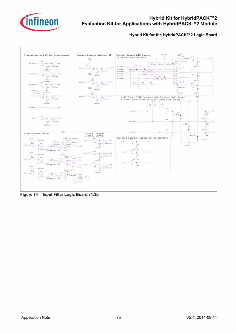
Hybrid Kit for HybridPACK™2Evaluation Kit for Applications with HybridPACK™2 Module
Hybrid Kit for the HybridPACK™2 Logic Board
Application Note 75 V2.4, 2014-08-11
Figure 74 Input Filter Logic Board v1.3b
R 22 3
6K 8
R 21 4
6K 8
C 1 1 60
1 00 n / 16 V / X 7R
C 1 0 41
1 0 p/ 5 0 V / X7 R
R 43 0
10 0R
GN D _ D I G1
General Purpose
+
-
V+
V-
I C 31 AL T 16 3 9H S
P A C K A G E = 13
21
411
+
-
I C 31 BL T 16 3 9H S
P A C K A GE = 1
5
67
C 1 04 2
1 0p / 5 0V / X 7 R
+
-
I C 31 DL T 16 3 9H S
P A C K A GE = 1
1 2
1 31 4
+
-
I C 31 CL T 16 3 9H S
P A C K A GE = 1
1 0
98
R 2 17
6 K 8
I C 3 3
A M 26 C 3 2 QD
1 A +2
1Y3
Vc
c1
6GN
D8
1 B -1
2 A +6
2 B -7
3 A +10
3 B -9
4 A +14
4 B -15
2Y5
3Y 11
4Y13
G+4
G-12
R 43 1
1 0 0R
Encoder Inputs/iGMR Inputs (iGMR Emulates Encoder)
C 1 7 21 n/ 5 0 V / X7 R
GN D _ A N A 1
R 1 75
6 8 KR 1 76op t
C 1 7 61 n/ 5 0 V / X7 RR 1 85
op t
GN D _ A N A 1
R 1 8 4
6 8 K
C 1 8 01 n/ 5 0 V / X7 R
GN D _ A N A 1
R 1 9 1
6 8 KR 1 94op t
C 1 8 31 n/ 5 0 V / X7 RR 2 02
op t
GN D _ A N A 1
R 2 28
6 K 8
R 1 9 8
6 8 K
C 1 8 71 n/ 5 0 V / X7 R
GN D _ A N A 1
R 2 0 5
6 8 KR 2 08op t
S t at o rT em p
C 1 9168 0 0p / 1 0V / C 0G
V D C
C 1 9468 0 0p / 1 0V / C 0G
C 1 9668 0 0p / 1 0V / C 0G
T E MP _ I GB T _U
T E MP _ I GB T _W
T E MP _ I GB T _V
I _ V
I _ U
A N 1 3
A N 14
A N 1 5
I _ W
A N 1
A N 4
A N 3
A N 2
GN D _A N A 1
G N D _ A N A 1
A N 2 9
R 2 35
6 K 8
Digital IN/OUT
G N D _ A N A 1
R 2 1 5
3 K 3
D I O_ 1C 1 1 61
1 0 0n / 1 6V / X 7 R
GN D _A N A 1
General Purpose Analogue IN
G N D _ D I G 1
R 1 74
1 0K
V A N A 5 0+5 . 0 V
V A N A 5 0+5 . 0 V
Temperature and DC Bus Measurements V D I G5 0+ 5 . 0V
C 1 7910 0 p/ 5 0 V / X7 RR 1 9 3
9 1K
R 1 89
5 1K
R 2 0 09 1K
R 1 96
5 1K C 1 8210 0 p/ 5 0 V / X7 R
G N D _ D I G1
G N D _ D I G1
G N D _ D I G1
C 1 7410 0 p/ 5 0 V / X7 RR 1 8 2
9 1K
R 1 79
5 1K
D I O_ 2
R 1 8 0
1 KR 1 832K
P 0_ 1 4
R 1 902K
P 0_ 1 1
R 1 8 7
1 K
R 2 012K
R 1 9 7
1 K
GN D _D I G1
GN D _D I G1
R 48 1
op tG N D _ A N A 1
D I O_ 3
GN D _D I G1
P 0_ 1 2
R 2 372K
R 1 81op t
GN D _ A N A 1
R 2 3 4
1 K
P 1 _1 0
R 17 85 1 K C 1 7 3
1 n/ 5 0 V / X7 R
P 4 _3
A N 17A D C _ I N 1
R 2 3 8
1 KR 2 392K
R 2 4 0
1 KR 2 412K
N M
B
A
GN D _D I G1
GN D _D I G1
P 1 _8
R 4 7 2
3 K 3
C 10 4 41 0 p/ 5 0 V / X7 R
R 2 1 8
3 K 3
R 1 92op t
GN D _ A N A 1
R 1 8 8
5 1 K C 1 7 81 n/ 5 0 V / X7 R
G N D _ A N A 1
R 48 0
op t
C 1 04 510 p / 50 V / X 7RR 1 77
10 K
C 1 0 431 0p / 5 0V / X 7 R
GN D _ A N A 1
C 1 8 41 n/ 5 0 V / X7 RR 2 03
op t
R 1 9 9
5 1 K
Phase Current Sense
A N 31
R 2 2 9
0R
P o sA / i GM R _ A +
Emulated encoder outputs out of AD2S1200
P o sZ / i GM R _ Z -
P o sB / i GM R _ B -
P o sA / i GM R _ A -
P o sZ / i GM R _ Z +
P o sB / i GM R _ B +
A D C _ I N 2
R 47 7
op t
A D C _ I N 3
R 1 8 61 0K
L 12MU R A TA _ B L M2 1P G 22 1 S N
P 4 _1
C 10 6 43 3 00 p / 10 V / C 0 G
R 1 9 51 0K
G N D _ A N A 1
R 2 2 4
0R _o p t
C 10 6 53 3 00 p / 10 V / C 0 G
A N 18
C 10 6 73 3 00 p / 10 V / C 0 G
A N 19
P 4 _0
R 4 29
10 0 R
A N 5T E MP _ B oa rd
C 1 0 40
1 0 p/ 5 0 V / X7 R
P 2 _5
GN D _ D I G1
V A N A 5 0+ 5 . 0V
V A N A 5 0+ 5 . 0V
V A N A 5 0+ 5 . 0V
GN D _ A N A 1
GN D _ A N A 1
GN D _ A N A 1
C 1 14 810 p / 50 V / X 7R
C 11 4 71 0 p/ 5 0 V / X7 R
C 1 14 91 0p / 50 V / X 7R
R 4 96
1K
G N D _ D I G 1
G N D _ A N A 1
R 4 912 K 7
P o s V / iG MR _ V
P o s U / i GMR _U
Hall Sensor/iGMR Inputs (iGMR Emulates Hall Sensor)Assumed Open-Collector output from Hall sensor
P o s W / iG MR _ W
V D I G 33+ 3 . 3V
P 2 _ 2
C 1 2 13o pt
P 4 _ 2
P 2 _ 0
C 1 2 15o pt
C 1 2 14o pt
R 49 22 K 7
R 49 32 K 7
GN D _D I G1
D 7B A T 54 -0 4W
GN D _D I G1
D 8B A T 5 4-0 4 W
GN D _D I G1
D 9B A T5 4 -04 W
R 4 94
1K
R 4 95
1K
G N D _ A N A 1
R 48 2
0R
R 23 0
6K 8
R 47 9
0 R
R 47 8
0R
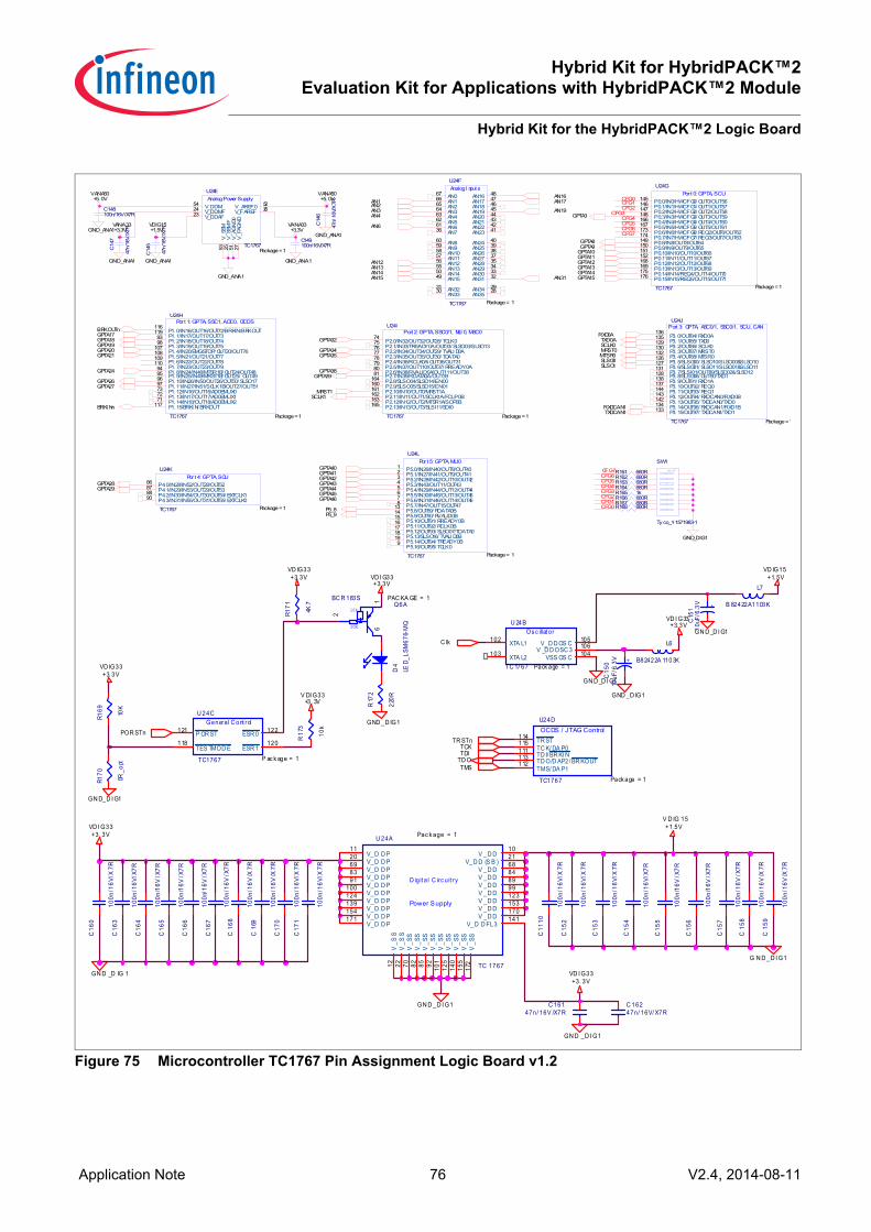
Hybrid Kit for HybridPACK™2Evaluation Kit for Applications with HybridPACK™2 Module
Hybrid Kit for the HybridPACK™2 Logic Board
Application Note 76 V2.4, 2014-08-11
Figure 75 Microcontroller TC1767 Pin Assignment Logic Board v1.2
GND_ANA1
GPTA39
BRKOUTn
GPTA24
C148100n/16V/X7R
C14
6
47n/
16V/
X7R
C14
7
47n/
16V
/X7R
CFG7
CFG5CFG6
CFG0
CFG4CFG3CFG2CFG1
AN15AN14
GPTA12
GPTA38
GPTA27GPTA26
VANA50+5. 0V
GPTA19
GPTA15GPTA14GPTA13
GPTA20
GPTA8GPTA9
AN1
GND_ANA1
GND_ANA1
AN6
AN3
GPTA40
AN4
GPTA18
SW1
Ty co_1-1571983-1
AN13
SLSO0
RXD0ATXD0A
SCLK1
MTSR0MRST0
MRST1
SCLK0
SLSO1
TXDCAN1RXDCAN1
GPTA41
GND_DIG1
AN16
VDIG15+1.5V
AN17
C14
5
47n/
16V
/X7R
R161 680R
GPTA32
GPTA34
GPTA17
AN19
Analog Power SupplyU24E
TC1767Package = 1
V_DDM54V_DDMF24V_DDAF23
V_S
SM53
V_S
SMF
25V
_AG
ND0
51V
_FAG
ND
27
V_AREF0 52V_FAREF 26
GND_ANA1
GPTA21
R162 680RR163 680R
Analog I nput sU24F
TC1767 Package = 1
AN067AN166AN265AN364AN463AN562AN661AN736
AN860AN959AN1058AN1157AN1256AN1355AN1450AN1549
AN16 48AN17 47AN18 46AN19 45AN20 44AN21 43AN22 42AN23 41
AN24 40AN25 39AN26 38AN27 37AN28 35AN29 34AN30 33AN31 32
AN3231AN33
30 AN34 29AN35
28
R164 680R
Port 0: GPTA, SCUU24G
TC1767 Package = 1
P0.0/IN0/HWCFG0/ OUT0/OUT56145P0.1/IN1/HWCFG1/ OUT1/OUT57146P0.2/IN2/HWCFG2/ OUT2/OUT58147P0.3/IN3/HWCFG3/ OUT3/OUT59148P0.4/IN4/HWCFG4/ OUT4/OUT60166P0.5/IN5/HWCFG5/ OUT5/OUT61167P0.6/IN6/HWCFG6/ REQ2/OUT6/OUT62173P0.7/IN7/HWCFG7/ REQ3/OUT7/OUT63174P0.8/IN8/OUT8/OUT64149P0.9/IN9/OUT9/OUT65150P0.10/IN10/OUT10/OUT66151P0.11/IN11/OUT11/OUT67152P0.12/IN12/OUT12/OUT68168P0.13/IN13/OUT13/OUT69169P0.14/IN14/REQ4/OUT14/OUT70175P0.15/IN15/REQ5/OUT15/OUT71176
GPTA35
Por t 1: GPTA, SSC1, ADC0, OCDSU24H
TC1767 Package = 1
P1. 0/IN16/OUT16/OUT72/BRKIN/BRKOUT116
P1. 1/IN17/OUT17/OUT73119
P1. 2/IN18/OUT18/OUT7493
P1. 3/IN19/OUT19/OUT7598
P1. 4/IN20/EMGSTOP/ OUT20/OUT76107
P1. 5/IN21/OUT21/OUT77108
P1. 6/IN22/OUT22/OUT78109
P1. 7/IN23/OUT23/OUT79110
P1. 8/IN24/IN48/MTSR1B/ OUT24/OUT4894
P1. 9/IN25/IN49/MRST1B/ OUT25/ OUT4995P1. 10/IN26/IN50/OUT26/OUT50/ SLSO1796P1. 11/IN27/IN51/SCLK1B/OUT27/OUT5197P1. 12/IN16/OUT16/AD0EMUX073P1. 13/IN17/OUT17/AD0EMUX172P1. 14/IN18/OUT18/AD0EMUX271P1. 15/BRKI N/ BRKOUT117
R165 1k
Port 2: GPTA, SSC0/1, MLI 0, MSC0U24I
TC1767 Package = 1
P2.0/IN32/OUT32/OUT28/ TCLK074
P2.1/IN33/TREADY0A/OUT33/ SLSO03/SLSO1375
P2.2/IN34/OUT34/OUT29/ TVALI D0A76
P2.3/IN35/OUT35/OUT30/ TDATA077
P2.4/IN36/RCLK0A/ OUT36/OUT3178
P2.5/IN37/OUT110/OUT37/ RREADY0A79
P2.6/IN38/RVALID0A/OUT111/OUT3880
P2.7/IN39/RDATA0A/OUT3981P2.8/SLSO04/SLSO14/EN00164P2.9/SLSO05/SLSO15/EN01160P2.10/IN10/OUT0/MRST1A161P2.11/IN11/OUT1/SCLK1A/FCLP0B162P2.12/IN12/OUT2/MTSR1A/SOP0B163P2.13/IN13/OUT3/SLSI11/SDI0165
C149100n/16V/X7R
R166 680R
Port 3: GPTA, ASC0/1, SSC0/1, SCU, CANU24J
TC1767 Package = 1
P3. 0/OUT84/ RXD0A136
P3. 1/OUT85/ TXD0135
P3. 2/OUT86/ SCLK0129
P3. 3/OUT87/ MRST0130
P3. 4/OUT88/ MTSR0132
P3. 5/SLSO00/ SLSO10/SLSO00&SLSO10126
P3. 6/SLSO01/ SLSO11/SLSO01&SLSO11127
P3. 7/SLSI01/OUT89/SLSO02&SLSO12131
P3. 8/SLSO06/ OUT90/TXD1128P3. 9/OUT91/ RXD1A138P3. 10/OUT92/ REQ0137P3. 11/OUT93/ REQ1144P3. 12/OUT94/ RXDCAN0/RXD0B143P3. 13/OUT95/ TXDCAN0/TXD0142P3. 14/OUT96/ RXDCAN1/RXD1B134P3. 15/OUT97/ TXDCAN1/TXD1133
R167 680R
Port 4: GPTA, SCUU24K
TC1767 Package = 1
P4. 0/IN28/IN52/OUT28/OUT5286P4. 1/IN29/IN53/OUT29/OUT5387P4. 2/IN30/IN54/OUT30/OUT54/ EXTCLK188P4. 3/IN31/IN55/OUT31/OUT55/ EXTCLK090
GND_ANA1
Por t 5: GPTA, MLI0U24L
TC1767 Package = 1
P5.0/IN26/IN40/OUT8/OUT401P5.1/IN27/IN41/OUT9/OUT412P5.2/IN28/IN42/OUT10/OUT423P5.3/IN43/OUT11/OUT434P5.4/IN29/IN44/OUT12/OUT445P5.5/IN30/IN45/OUT13/OUT456P5.6/IN31/IN46/OUT14/OUT467P5.7/IN47/OUT15/OUT478P5.8/OUT89/ RDATA0B
13
P5.9/OUT90/ RVALID0B14
P5.10/OUT91/ RREADY0B15
P5.11/OUT92/ RCLK0B16
P5.12/OUT93/ SLSO07/TDATA017
P5.13/SLSO16/ TVALI D0B18
P5.14/OUT94/ TREADY0B19
P5.16/OUT95/ TCLK09
R168 680R
VANA33+3.3V
VANA50+5. 0V
AN2
GPTA28
CFG0
CFG6CFG7
CFG5
CFG1
AN31
GPTA11
GPTA3CFG2
CFG3CFG4
GPTA43GPTA29
GPTA45
GPTA10
GPTA42
P5_8
GPTA44
BRKI Nn
GPTA46
AN12
GND_ANA1
VANA33+3.3V
P5_9
POR STn
R17
3
10k
V DI G33+3. 3V R
172
220R
GND _D IG1
D4
LED_
LSM
676-
MQ
VD I G33+3.3V
10k
10kQ6A
BC R 183S PAC KA GE = 1
2
16
R171 4K
7
VD IG33+3. 3V
L6
B82422A 1103K
R170
0R_o
pt
L7
B 82422A1103K
R169 10K
VD I G33+3. 3V
C lk
VD IG15+1. 5V
GN D_D I G1
VD IG33+3. 3V
GND _D IG1
GN D _D I G1Os c illat orU 24B
TC 1767 Pack age = 1
XTA L1102
XTA L2103V_D D OS C 105
V _D D OSC 3 106
VSS OS C 104
General C ont rolU 24C
TC1767 P ac k age = 1
P OR ST121
TES TMOD E118
ESR 0 122
ESR 1120
OCDS / JTAG ControlU24D
TC1767 Pack age = 1
TR ST114
TC K/ DA P0115
TD I/ BR KI N111TD O/D AP2/ BR KOUT113
TMS/ DA P1112
GN D _D I G1
+
C15
010
uF/6
.3V
+
C15
110
uF/6
.3V
TR STnTCK
TMS
TDITD O
C17
0
100n
/16V
/X7R
C16
8
100n
/16V
/X7R
C15
9
100n
/16V
/X7R
C15
8
100n
/16V
/X7R
C16
7
100n
/16V
/X7R
C16
6
100n
/16V
/X7R
C15
3
100n
/16V
/X7R
C16
5
100n
/16V
/X7R
C15
4
100n
/16V
/X7R
C17
1
100n
/16V
/X7R
C16
4
100n
/16V
/X7R
C16
0
100n
/16V
/X7R
C15
5
100n
/16V
/X7R
C 16147n/ 16V /X7R
C15
6
100n
/16V
/X7R
C16
3
100n
/16V
/X7R
C16
9
100n
/16V
/X7R
C15
7
100n
/16V
/X7R
G N D _D I G1
GN D _D I G1
VD I G33+3. 3V
GN D _D IG 1 VD I G33+3. 3V
GN D _D I G1
V D IG 15+1.5V
C15
2
100n
/16V
/X7R
C 16247n/ 16V/ X7R
D igit a l C irc uit ry
Power Supply
U 24A
TC 1767
Pac k age = 1
V_D D P11
V_D D P20
V_D D P69
V_D D P83
V_D D P91
V_D D P100
V_D D P124
V_D D P139
V_D D P154
V_D D P171
V_S
S12
V_S
S22
V_S
S70
V_S
S82
V_S
S85
V_S
S92
V_S
S10
1
V_S
S12
5
V_S
S14
0
V_S
S15
5
V_S
S17
2
V _D D10
V_D D (S B )21
V _D D68
V _D D84
V _D D99
V _D D123
V _D D153
V _D D170
V_D D FL3141
V _D D89
C11
10
100n
/16V
/X7R

Hybrid Kit for HybridPACK™2Evaluation Kit for Applications with HybridPACK™2 Module
Hybrid Kit for the HybridPACK™2 Logic Board
Application Note 77 V2.4, 2014-08-11
Figure 76 Microcontroller TC1767 Pin Assignment Logic Board v1.3b
GND_ANA1
VANA33+3.3V
P5_0
GPTA39
BRKOUTn
P1_8
GND_ANA1
P5_1P5_2
P5_4P5_3
P5_5
GND_ANA1
P0_14
P5_6
P5_11P5_10P5_9P5_8P5_7
R499 100kR500 100k
P5_15
R502 100kR501 100k
R504 100kR503 100k
R506 100kR505 100k
VDI G33+3.3V
C148100n/16V/X7R
C146
47n/
16V/
X7R
C14
7
47n/
16V
/X7R
CFG7
CFG5CFG6
CFG0
CFG4CFG3CFG2CFG1
AN15AN14
P0_12
GPTA27
VANA50+5. 0V
GPTA19GPTA20
GPTA8GPTA9
AN1
GND_ANA1
GND_REF1
VANA33+3.3V
P1_5
P4_2
P1_6P1_7
GND_ANA1
AN3
P2_0
AN4
P5_13P5_12
GPTA18
P2_12
SW1
Ty co_1-1571983-1
AN13
SLSO0
RXD0ATXD0A
SCLK1
MTSR0MRST0
MRST1
SCLK0
SLSO1
TXDCAN1RXDCAN1
GND_DI G1
AN29
VANA15+1.5V
AN17
C14
5
47n/
16V
/X7R
R161 1K
AN19
Analog Power Supply
IC24ESAK-TC1767-256F133HL
Package = 1
V_DDM54
V_DDMF24
V_DDAF23
V_S
SM53
V_S
SMF
25V
_AG
ND0
51V
_FAG
ND
27
V_AREF052
V_FAREF26
GND_ANA1
P3_10
R162 1K
AN5
R163 1K
Analog I nputs
IC24FSAK-TC1767-256F133HL
Package = 1
AN067
AN166
AN265
AN364
AN463
AN562
AN661
AN736
AN860AN959AN1058AN1157AN1256AN1355AN1450AN1549
AN1648
AN1747
AN1846
AN1945
AN2044
AN2143
AN2242
AN2341
AN24 40AN25 39AN26 38AN27 37AN28 35AN29 34AN30 33AN31 32
AN3231AN3330 AN34 29
AN35 28
P4_1R164 1K
Port 0: GPTA, SCU
I C24GSAK-TC1767-256F133HL
Package = 1
P0.0/IN0/HWCFG0/OUT0/ OUT56145
P0.1/IN1/HWCFG1/OUT1/ OUT57146
P0.2/IN2/HWCFG2/OUT2/ OUT58147
P0.3/IN3/HWCFG3/OUT3/ OUT59148
P0.4/IN4/HWCFG4/OUT4/ OUT60166
P0.5/IN5/HWCFG5/OUT5/ OUT61167
P0.6/IN6/HWCFG6/REQ2/OUT6/OUT62173
P0.7/IN7/HWCFG7/REQ3/OUT7/OUT63174P0.8/IN8/OUT8/OUT64149P0.9/IN9/OUT9/OUT65150P0.10/IN10/OUT10/OUT66151P0.11/IN11/OUT11/OUT67152P0.12/IN12/OUT12/OUT68168P0.13/IN13/OUT13/OUT69169P0.14/IN14/REQ4/OUT14/OUT70175P0.15/IN15/REQ5/OUT15/OUT71176
R165 1K
Por t 1: GPTA, SSC1, ADC0, OCDSIC24H
SAK-TC1767-256F133HL Package = 1
P1. 0/IN16/OUT16/OUT72/ BRKIN/BRKOUT116P1. 1/IN17/OUT17/OUT73119P1. 2/IN18/OUT18/OUT7493P1. 3/IN19/OUT19/OUT7598P1. 4/IN20/EMGSTOP/OUT20/OUT76107P1. 5/IN21/OUT21/OUT77
108
P1. 6/IN22/OUT22/OUT78109
P1. 7/IN23/OUT23/OUT79110
P1. 8/IN24/IN48/MTSR1B/OUT24/OUT4894
P1. 9/IN25/IN49/MRST1B/OUT25/ OUT4995
P1. 10/IN26/IN50/OUT26/OUT50/ SLSO1796
P1. 11/IN27/IN51/SCLK1B/OUT27/OUT5197
P1. 12/IN16/OUT16/AD0EMUX073
P1. 13/IN17/OUT17/AD0EMUX172
P1. 14/IN18/OUT18/AD0EMUX271
P1. 15/BRKI N/ BRKOUT117
Port 2: GPTA, SSC0/1, MLI 0, MSC0IC24I
SAK-TC1767-256F133HL Package = 1
P2.0/IN32/OUT32/OUT28/TCLK074P2.1/IN33/TREADY0A/OUT33/SLSO03/SLSO1375P2.2/IN34/OUT34/OUT29/TVALI D0A76P2.3/IN35/OUT35/OUT30/TDATA0
77
P2.4/IN36/RCLK0A/OUT36/ OUT3178
P2.5/IN37/OUT110/OUT37/RREADY0A79
P2.6/IN38/RVALID0A/OUT111/OUT3880
P2.7/IN39/RDATA0A/OUT3981
P2.8/SLSO04/SLSO14/ EN00164
P2.9/SLSO05/SLSO15/ EN01160
P2.10/IN10/OUT0/MRST1A161
P2.11/IN11/OUT1/SCLK1A/FCLP0B162
P2.12/IN12/OUT2/MTSR1A/ SOP0B163
P2.13/IN13/OUT3/SLSI11/SDI 0165
C149100n/16V/X7R
R166 1K
Port 3: GPTA, ASC0/ 1, SSC0/1, SCU, CANIC24J
SAK-TC1767-256F133HL Package = 1
P3.0/OUT84/RXD0A136P3.1/OUT85/TXD0135P3.2/OUT86/SCLK0129P3.3/OUT87/MRST0130P3.4/OUT88/MTSR0
132
P3.5/SLSO00/SLSO10/ SLSO00&SLSO10126
P3.6/SLSO01/SLSO11/ SLSO01&SLSO11127
P3.7/SLSI01/OUT89/SLSO02&SLSO12131
P3.8/SLSO06/OUT90/ TXD1128
P3.9/OUT91/RXD1A138
P3.10/OUT92/REQ0137
P3.11/OUT93/REQ1144
P3.12/OUT94/RXDCAN0/ RXD0B143
P3.13/OUT95/TXDCAN0/TXD0142
P3.14/OUT96/RXDCAN1/ RXD1B134
P3.15/OUT97/TXDCAN1/TXD1133
R167 1K
Por t 4: GPTA, SCUIC24K
SAK-TC1767-256F133HL Package = 1
P4.0/IN28/IN52/OUT28/OUT5286P4.1/IN29/IN53/OUT29/OUT5387P4.2/IN30/IN54/OUT30/OUT54/EXTCLK188P4.3/IN31/IN55/OUT31/OUT55/EXTCLK090
GND_ANA1
Port 5: GPTA, MLI0IC24L
SAK-TC1767-256F133HL Package = 1
P5.0/IN26/IN40/OUT8/OUT401P5.1/IN27/IN41/OUT9/OUT412P5.2/IN28/IN42/OUT10/OUT423P5.3/IN43/OUT11/OUT434P5.4/IN29/IN44/OUT12/OUT445P5.5/IN30/IN45/OUT13/OUT456P5.6/IN31/IN46/OUT14/OUT467P5.7/IN47/OUT15/OUT478P5.8/OUT89/RDATA0B13P5.9/OUT90/RVALI D0B14P5.10/OUT91/RREADY0B15P5.11/OUT92/RCLK0B16P5.12/OUT93/SLSO07/TDATA017P5.13/SLSO16/TVALID0B18P5.14/OUT94/TREADY0B19P5.16/OUT95/TCLK09
R168 1K
P4_0
Vref 50+5. 0V
AN2CFG0
P3_13
CFG6CFG7
CFG5
CFG1
GND_ANA1
AN31
P0_11
GPTA3CFG2CFG3
P2_2
P2_5
GND_REF1
CFG4
GND_ANA1
P1_10
SLSO2P3_8
AN18
P4_3
P3_11
BRKI Nn
GND_ANA1
GND_ANA1
P3_12
P1_9
P OR STn
R17
3
10K
VD I G33+3. 3V R
172
220R
GN D _D IG1
D4
LED_
LSM
676-
MQ
V D I G33+3. 3V
10k
10kQ6A
BC R 183S PA C KA GE = 1
2
1
6
R17
1
4K7
VD I G33+3.3V
L6
B82422A 1103K
R17
0
0R_o
pt
L7
B82422A 1103K
R16
9
10K
VD I G33+3.3V
C lk
VD I G15+1.5V
GN D _D I G1
V D IG33+3. 3V
GN D _D I G1
GN D _D I G1Os c illa t or
I C 24BS AK -TC 1767-256F133H L
Pac k age = 1
XTAL1102
XTAL2103
V_D D OSC105
V_D D OSC 3 106
VSS OSC104
General C ontrol
I C 24CSA K-TC 1767-256F133H L
P ack age = 1
POR S T121
TESTMOD E118ES R 0 122
ES R 1 120
OCDS / JTAG Cont rol
I C 24DSA K-TC 1767-256F133H L
Pac k age = 1
TR ST114
TC K/ D AP0115
TD I/ BR K IN111
TD O/ D A P2/B R KOU T113
TMS/ D AP1112
GN D_D I G1
TR S TnTC K
TMS
TD ITD O
C 15010u/ 10V/ X7R
C 15110u/ 10V/ X7R
C17
0
100n
/16V
/X7R
C16
8
100n
/16V
/X7R
C15
9
100n
/16V
/X7R
C15
8
100n
/16V
/X7R
C16
7
100n
/16V
/X7R
C16
6
100n
/16V
/X7R
C15
3
100n
/16V
/X7R
C16
5
100n
/16V
/X7R
C15
4
100n
/16V
/X7R
C17
1
100n
/16V
/X7R
C16
4
100n
/16V
/X7R
C16
0
100n
/16V
/X7R
C15
5
100n
/16V
/X7R
C 161100n/ 16V/ X7R
C15
6
100n
/16V
/X7R
C16
3
100n
/16V
/X7R
C16
9
100n
/16V
/X7R
C15
7
100n
/16V
/X7R
GN D _D IG 1
G N D _D I G1
VD I G33+3. 3V
GN D _D IG 1 V D I G33+3.3V
GN D _D I G1
V D I G15+1. 5V
C15
2
100n
/16V
/X7R
D ig it a l C irc uit ry
Power Supply
IC 24ASA K-TC 1767-256F 133H L
P ac k age = 1
V_D D P11
V_D D P20
V_D D P69
V_D D P83
V_D D P91
V_D D P100
V_D D P124
V_D D P139
V_D D P154
V_D D P171
V_S
S12
V_S
S22
V_S
S70
V_S
S82
V_S
S85
V_S
S92
V_S
S10
1
V_S
S12
5
V_S
S14
0
V_S
S15
5
V_S
S17
2
V _D D10
V _D D (S B)21
V _D D68
V _D D84
V _D D99
V _D D123
V _D D153
V _D D170
V_D D FL3141
V _D D89
C11
10
100n
/16V
/X7R

Hybrid Kit for HybridPACK™2Evaluation Kit for Applications with HybridPACK™2 Module
Hybrid Kit for the HybridPACK™2 Logic Board
Application Note 78 V2.4, 2014-08-11
Figure 77 EEPROM (same for Logic Board v1.2 and Logic Board v1.3b)
Figure 78 On-Board Temperature Measurement (Logic Board v1.3b only)
R 910K
R 810K
C29 10
0n/1
6V/X
7R
R 10opt
U 1
AT2 5256 A-10 TQ-2 .7C S 1SO 2
W P3
GN D4
SI5SC K 6
H OLD7
VC C8
R 710K
SC K
C Sn
S OSI
VD I G3 3+ 3.3 V
GN D _D IG1
Unit temperature sensor (Ambient)Position: bottom of Logic Board
Temp = 10mV/°C + 500mVTemp @ -40C: +100mV
Temp @ +125C: +1,750V
LPF: -3dB @ 32Hz
C12
1110
0n/5
0V/X
7R R 487
270K
C121222n/50V/X7R
GND
Vout
VCC
IC 54
LM50C IM3
2
3
1
Temp_Board
VANA50+5.0V
GND _AN A1
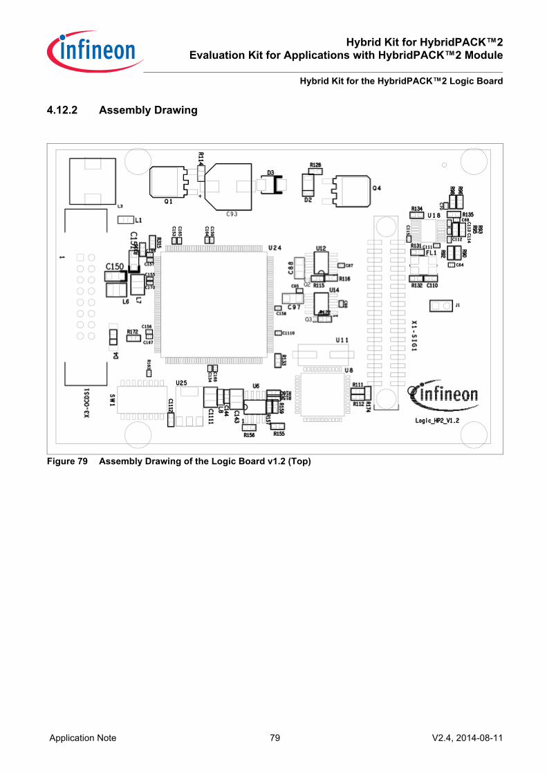
Hybrid Kit for HybridPACK™2Evaluation Kit for Applications with HybridPACK™2 Module
Hybrid Kit for the HybridPACK™2 Logic Board
Application Note 79 V2.4, 2014-08-11
4.12.2 Assembly Drawing
Figure 79 Assembly Drawing of the Logic Board v1.2 (Top)

Hybrid Kit for HybridPACK™2Evaluation Kit for Applications with HybridPACK™2 Module
Hybrid Kit for the HybridPACK™2 Logic Board
Application Note 80 V2.4, 2014-08-11
Figure 80 Assembly Drawing of the Logic Board v1.3b (Top)

Hybrid Kit for HybridPACK™2Evaluation Kit for Applications with HybridPACK™2 Module
Hybrid Kit for the HybridPACK™2 Logic Board
Application Note 81 V2.4, 2014-08-11
Figure 81 Assembly Drawing of the Logic Board v1.2 (Bottom)

Hybrid Kit for HybridPACK™2Evaluation Kit for Applications with HybridPACK™2 Module
Hybrid Kit for the HybridPACK™2 Logic Board
Application Note 82 V2.4, 2014-08-11
Figure 82 Assembly Drawing of the Logic Board v1.3b (Bottom)
For detail information use the zoom function of your PDF viewer to zoom into the drawings on Figure 79,Figure 80, Figure 81 and Figure 82.

Hybrid Kit for HybridPACK™2Evaluation Kit for Applications with HybridPACK™2 Module
Hybrid Kit for the HybridPACK™2 Logic Board
Application Note 83 V2.4, 2014-08-11
4.12.3 LayoutLayout of the Logic Board v1.2 is shown on Figure 83 (Top Layer), on Figure 84 (Layer 2), on Figure 85 (Layer3) and on Figure 86 (Bottom Layer).Layout of the Logic Board v1.3b is shown on Figure 87 (Top Layer), on Figure 88 (Layer 2), on Figure 89 (Layer3), on Figure 90 (Layer 4), on Figure 91 (Layer 5) and on Figure 92 (Bottom Layer).
Figure 83 Logic Board v1.2 - Top Layer

Hybrid Kit for HybridPACK™2Evaluation Kit for Applications with HybridPACK™2 Module
Hybrid Kit for the HybridPACK™2 Logic Board
Application Note 84 V2.4, 2014-08-11
Figure 84 Logic Board v1.2 - Layer 2
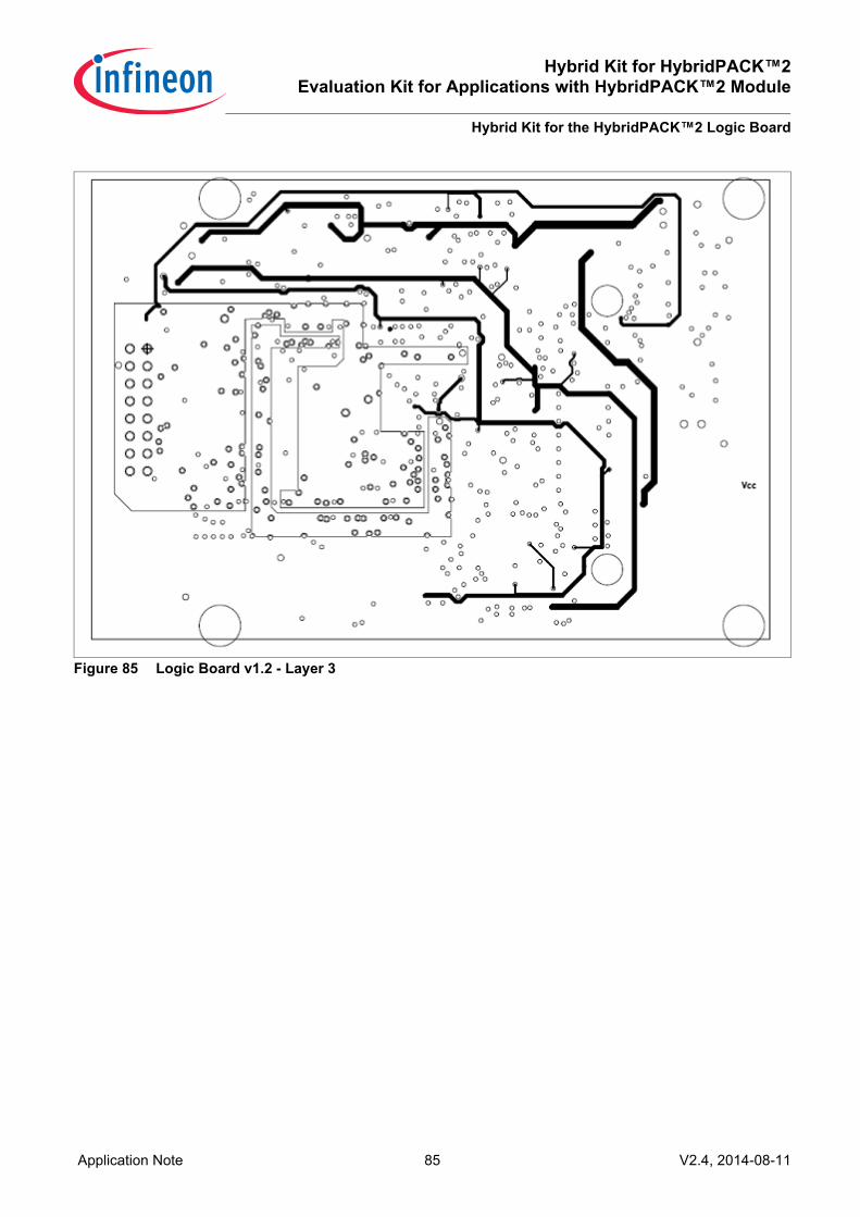
Hybrid Kit for HybridPACK™2Evaluation Kit for Applications with HybridPACK™2 Module
Hybrid Kit for the HybridPACK™2 Logic Board
Application Note 85 V2.4, 2014-08-11
Figure 85 Logic Board v1.2 - Layer 3

Hybrid Kit for HybridPACK™2Evaluation Kit for Applications with HybridPACK™2 Module
Hybrid Kit for the HybridPACK™2 Logic Board
Application Note 86 V2.4, 2014-08-11
Figure 86 Logic Board v1.2 - Bottom Layer

Hybrid Kit for HybridPACK™2Evaluation Kit for Applications with HybridPACK™2 Module
Hybrid Kit for the HybridPACK™2 Logic Board
Application Note 87 V2.4, 2014-08-11
Figure 87 Logic Board v1.3b - Top Layer
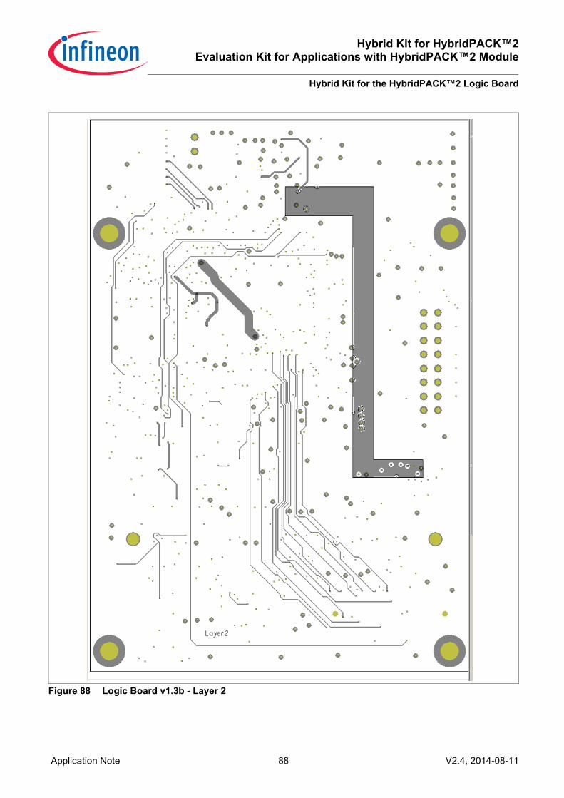
Hybrid Kit for HybridPACK™2Evaluation Kit for Applications with HybridPACK™2 Module
Hybrid Kit for the HybridPACK™2 Logic Board
Application Note 88 V2.4, 2014-08-11
Figure 88 Logic Board v1.3b - Layer 2

Hybrid Kit for HybridPACK™2Evaluation Kit for Applications with HybridPACK™2 Module
Hybrid Kit for the HybridPACK™2 Logic Board
Application Note 89 V2.4, 2014-08-11
Figure 89 Logic Board v1.3b - Layer 3

Hybrid Kit for HybridPACK™2Evaluation Kit for Applications with HybridPACK™2 Module
Hybrid Kit for the HybridPACK™2 Logic Board
Application Note 90 V2.4, 2014-08-11
Figure 90 Logic Board v1.3b - Layer 4

Hybrid Kit for HybridPACK™2Evaluation Kit for Applications with HybridPACK™2 Module
Hybrid Kit for the HybridPACK™2 Logic Board
Application Note 91 V2.4, 2014-08-11
Figure 91 Logic Board v1.3b - Layer 5

Hybrid Kit for HybridPACK™2Evaluation Kit for Applications with HybridPACK™2 Module
Hybrid Kit for the HybridPACK™2 Logic Board
Application Note 92 V2.4, 2014-08-11
Figure 92 Logic Board v1.3b - Bottom Layer
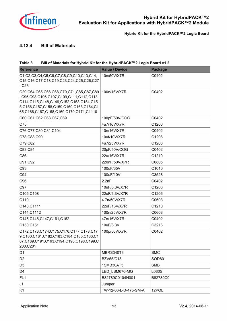
Hybrid Kit for HybridPACK™2Evaluation Kit for Applications with HybridPACK™2 Module
Hybrid Kit for the HybridPACK™2 Logic Board
Application Note 93 V2.4, 2014-08-11
4.12.4 Bill of Materials
Table 8 Bill of Materials for Hybrid Kit for the HybridPACK™2 Logic Board v1.2Reference Value / Device PackageC1,C2,C3,C4,C5,C6,C7,C8,C9,C10,C13,C14, C15,C16,C17,C18,C19,C23,C24,C25,C26,C27, C28
10n/50V/X7R C0402
C29,C64,C65,C66,C68,C70,C71,C85,C87,C89, C95,C98,C106,C107,C109,C111,C112,C113, C114,C115,C148,C149,C152,C153,C154,C155,C156,C157,C158,C159,C160,C163,C164,C165,C166,C167,C168,C169,C170,C171,C1110
100n/16V/X7R C0402
C60,C61,C62,C63,C67,C69 100pF/50V/COG C0402C75 4u7/16V/X7R C1206C76,C77,C80,C81,C104 10n/16V/X7R C0402C78,C88,C90 10uf/10V/X7R C1206C79,C82 4u7/25V/X7R C1206C83,C84 20pF/50V/COG C0402C86 22u/16V/X7R C1210C91,C92 220nF/50V/X7R C0805C93 100uF/35V C1010C94 100uF/10V C3528C96 2.2nF C0402C97 10uF/6.3V/X7R C1206C105,C108 22uF/6.3V/X7R C1206C110 4.7n/50V/X7R C0603C143,C1111 22uF/16V/X7R C1210C144,C1112 100n/25V/X7R C0603C145,C146,C147,C161,C162 47n/16V/X7R C0402C150,C151 10uF/6.3V C3216C172,C173,C174,C175,C176,C177,C178,C179,C180,C181,C182,C183,C184,C185,C186,C187,C189,C191,C193,C194,C196,C198,C199,C200,C201
100p/50V/X7R C0402
D1 MBRS340T3 SMCD2 BZV55/C13 SOD80D3 1SMB30AT3 SMBD4 LED_LSM676-MQ L0805FL1 B82789C0104N001 B82789C0J1 JumperK1 TW-12-06-L-D-475-SM-A 12POL

Hybrid Kit for HybridPACK™2Evaluation Kit for Applications with HybridPACK™2 Module
Hybrid Kit for the HybridPACK™2 Logic Board
Application Note 94 V2.4, 2014-08-11
L1,L2,L5,L8 MURATA_BLM21P221SN L0805L3 47uH/B82464G4473M B82464G4L6,L7 B82422A1103K C1210Q1 SPD09P06PLG TO252-3Q2,Q3 BC847BL3 TSLP3-1Q4 IPD90P03P4L-04 TO252-003Q6 BCR183S SOT363R1,R2,R3,R4,R5,R6,R101,R115,R116,R118, R122,R128,R169,R174,R177,R186,R195
10K R0603
R7,R8,R9,R71,R73,R173 10K R0402R10 opt R0402R72,R87,R89,R91,R94,R97 100R R0603R74,R75,R76,R77,R78,R79,R80,R81,R82,R83, R84,R85,R86,R88,R165
1K R0402
R90,R93,R96,R99 15K R0603R92,R95,R98,R100,R134,R135 1K R0603R102,R104,R106,R108,R121,R224,R316 0R R0603R103,R105,R107,R109,R110,R149,R154,R176,R181,R185,R192,R194,R202,R203,R208,R217,R228,R235,R236
opt R0603
R111 20K R0603R112 39K R0603R113 0R R1210R114 47mR/0.33W R0805R119 680R R0603R131,R132 60R R0603R133 5K1 R0603R150,R151,R153,R171 4K7 R0603R155,R156,R157,R158,R159,R160 opt R0603R161,R162,R163,R164,R166,R167,R168 680R R0402R170,R229,R315 0R_opt R0603R172 220R R0603R175,R178,R179,R180,R184,R187,R188,R189,R191,R196,R197,R198,R199,R204,R205,R206,R213,R214,R222,R223,R230,R231,R234,R238,R240
51K R0603
R182,R183,R190,R193,R200,R201,R207,R210,R216,R227,R237,R239,R241
91K R0603
SW1 Tyco_1-1571983-1 DIPU1 AT25256A-10TQ-2.7 TSSOP-08
Table 8 Bill of Materials for Hybrid Kit for the HybridPACK™2 Logic Board v1.2 (cont’d)
Reference Value / Device Package
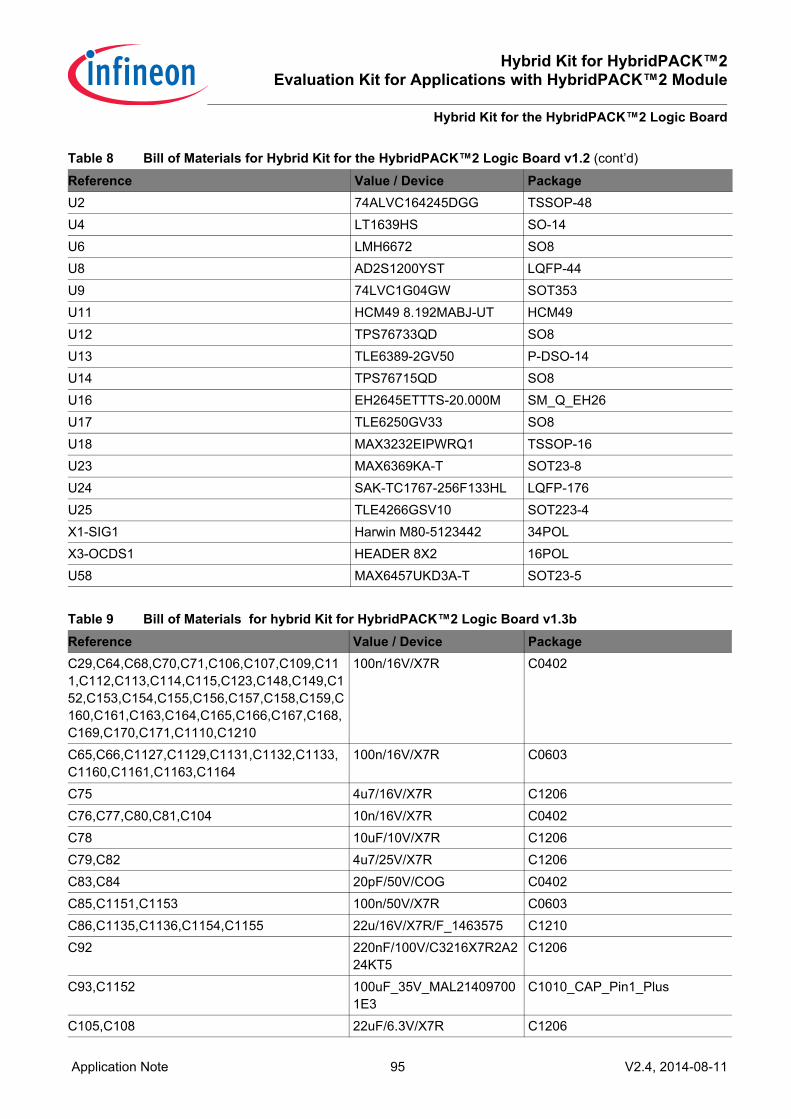
Hybrid Kit for HybridPACK™2Evaluation Kit for Applications with HybridPACK™2 Module
Hybrid Kit for the HybridPACK™2 Logic Board
Application Note 95 V2.4, 2014-08-11
U2 74ALVC164245DGG TSSOP-48U4 LT1639HS SO-14U6 LMH6672 SO8U8 AD2S1200YST LQFP-44U9 74LVC1G04GW SOT353U11 HCM49 8.192MABJ-UT HCM49U12 TPS76733QD SO8U13 TLE6389-2GV50 P-DSO-14U14 TPS76715QD SO8U16 EH2645ETTTS-20.000M SM_Q_EH26U17 TLE6250GV33 SO8U18 MAX3232EIPWRQ1 TSSOP-16U23 MAX6369KA-T SOT23-8U24 SAK-TC1767-256F133HL LQFP-176U25 TLE4266GSV10 SOT223-4X1-SIG1 Harwin M80-5123442 34POLX3-OCDS1 HEADER 8X2 16POLU58 MAX6457UKD3A-T SOT23-5
Table 9 Bill of Materials for hybrid Kit for HybridPACK™2 Logic Board v1.3bReference Value / Device PackageC29,C64,C68,C70,C71,C106,C107,C109,C111,C112,C113,C114,C115,C123,C148,C149,C152,C153,C154,C155,C156,C157,C158,C159,C160,C161,C163,C164,C165,C166,C167,C168,C169,C170,C171,C1110,C1210
100n/16V/X7R C0402
C65,C66,C1127,C1129,C1131,C1132,C1133,C1160,C1161,C1163,C1164
100n/16V/X7R C0603
C75 4u7/16V/X7R C1206C76,C77,C80,C81,C104 10n/16V/X7R C0402C78 10uF/10V/X7R C1206C79,C82 4u7/25V/X7R C1206C83,C84 20pF/50V/COG C0402C85,C1151,C1153 100n/50V/X7R C0603C86,C1135,C1136,C1154,C1155 22u/16V/X7R/F_1463575 C1210C92 220nF/100V/C3216X7R2A2
24KT5C1206
C93,C1152 100uF_35V_MAL214097001E3
C1010_CAP_Pin1_Plus
C105,C108 22uF/6.3V/X7R C1206
Table 8 Bill of Materials for Hybrid Kit for the HybridPACK™2 Logic Board v1.2 (cont’d)
Reference Value / Device Package
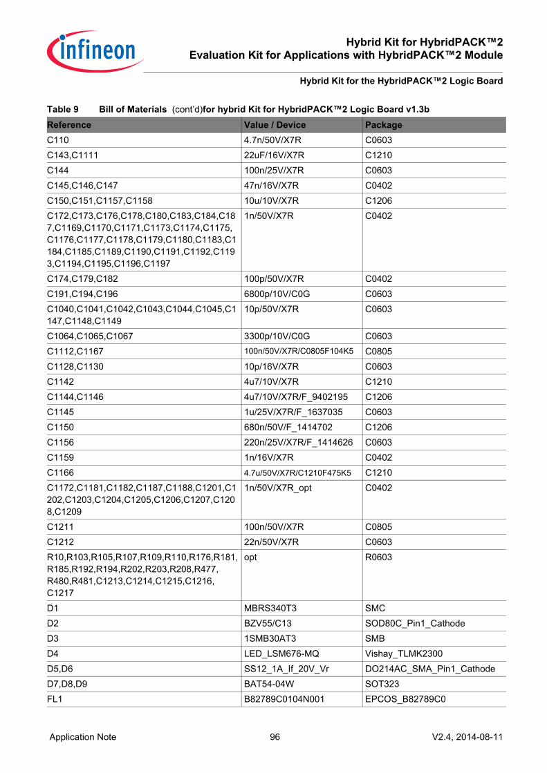
Hybrid Kit for HybridPACK™2Evaluation Kit for Applications with HybridPACK™2 Module
Hybrid Kit for the HybridPACK™2 Logic Board
Application Note 96 V2.4, 2014-08-11
C110 4.7n/50V/X7R C0603C143,C1111 22uF/16V/X7R C1210C144 100n/25V/X7R C0603C145,C146,C147 47n/16V/X7R C0402C150,C151,C1157,C1158 10u/10V/X7R C1206C172,C173,C176,C178,C180,C183,C184,C187,C1169,C1170,C1171,C1173,C1174,C1175,C1176,C1177,C1178,C1179,C1180,C1183,C1184,C1185,C1189,C1190,C1191,C1192,C1193,C1194,C1195,C1196,C1197
1n/50V/X7R C0402
C174,C179,C182 100p/50V/X7R C0402C191,C194,C196 6800p/10V/C0G C0603C1040,C1041,C1042,C1043,C1044,C1045,C1147,C1148,C1149
10p/50V/X7R C0603
C1064,C1065,C1067 3300p/10V/C0G C0603C1112,C1167 100n/50V/X7R/C0805F104K5 C0805C1128,C1130 10p/16V/X7R C0603C1142 4u7/10V/X7R C1210C1144,C1146 4u7/10V/X7R/F_9402195 C1206C1145 1u/25V/X7R/F_1637035 C0603C1150 680n/50V/F_1414702 C1206C1156 220n/25V/X7R/F_1414626 C0603C1159 1n/16V/X7R C0402C1166 4.7u/50V/X7R/C1210F475K5 C1210C1172,C1181,C1182,C1187,C1188,C1201,C1202,C1203,C1204,C1205,C1206,C1207,C1208,C1209
1n/50V/X7R_opt C0402
C1211 100n/50V/X7R C0805C1212 22n/50V/X7R C0603R10,R103,R105,R107,R109,R110,R176,R181,R185,R192,R194,R202,R203,R208,R477,R480,R481,C1213,C1214,C1215,C1216,C1217
opt R0603
D1 MBRS340T3 SMCD2 BZV55/C13 SOD80C_Pin1_CathodeD3 1SMB30AT3 SMBD4 LED_LSM676-MQ Vishay_TLMK2300D5,D6 SS12_1A_If_20V_Vr DO214AC_SMA_Pin1_CathodeD7,D8,D9 BAT54-04W SOT323FL1 B82789C0104N001 EPCOS_B82789C0
Table 9 Bill of Materials (cont’d)for hybrid Kit for HybridPACK™2 Logic Board v1.3bReference Value / Device Package

Hybrid Kit for HybridPACK™2Evaluation Kit for Applications with HybridPACK™2 Module
Hybrid Kit for the HybridPACK™2 Logic Board
Application Note 97 V2.4, 2014-08-11
IC1 AT25256A-10TQ-2.7 TSSOP8IC2 74ALVC164245DGG TSSOP48IC4,IC31 LT1639HS SO14IC6 LMH6672 SO8IC8 AD2S1200YST LQFP44_P0_8IC13 TLE7368E SO36-38IC16 EH2645ETTTS-20.000M Ecliptek_EH2645IC17 TLE6250GV33 SO8IC23 MAX6369KA-T SOT23-8IC24 SAK-TC1767-256F133HL LQFP176_p0_50IC25 TLE4266GSV10 SOT223IC26 DS92LV010 SO8IC28,IC30 74LVC2G04GW SOT363IC29 74LVCH16T245DL SSOP48IC32 DS90LV031A SO16-1IC33 AM26C32QD SO16-1IC52 MAX3232EIPWRQ1 TSSOP16IC53 MAX6143AASA50 SO8IC54 LM50CIM3 SOT23J1 Jumper jumper_2wayK1 TW-12-06-L-D-475-SM-A Samtec_TW-12-06-L-D-475-SM-A
K2 Harwin M80-5125042P Harwin_M80-5125042PK3-OCDS HEADER 8X2 tyco_1761686-6L1,L8,L9,L10,L11,L12 MURATA_BLM21PG221SN L0805L3 WE_7447709470 WE-PD_744770L5 MURATA_BLM21P221SN L0805L6,L7 B82422A1103K L1210Q2 BDP949 SOT223Q4 IPD90P03P4L-04 TO252-3Q6 BCR183S SOT363R1,R2,R3,R4,R5,R6,R7,R8,R9,R71,R73,R173,R174,R177,R186,R195,R471,R473,R474,R475,R476
10K R0402
R74,R75,R76,R77,R78,R79,R80,R88,R92,R95,R98,R100,R134,R135,R161,R162,R163,R164,R165,R166,R167,R168,R180,R187,R197,R234,R238,R240,R456
1K R0402
R90,R93,R96,R99 15K R0402R101,R128,R169 10K R0603
Table 9 Bill of Materials (cont’d)for hybrid Kit for HybridPACK™2 Logic Board v1.3bReference Value / Device Package

Hybrid Kit for HybridPACK™2Evaluation Kit for Applications with HybridPACK™2 Module
Hybrid Kit for the HybridPACK™2 Logic Board
Application Note 98 V2.4, 2014-08-11
R102,R104,R106,R108,R478,R479,R482,R497
0R R0603
R113 SMK-R000 / Isabellenhuette R1206R131,R132 60R R0603R133 5K1 R0402R149,R154 opt R0402R150,R151,R153 4K7 R0402R155,R156,R158,R160 2K4/0.1% R0603R157 390/0.1% R0603R159 3K3/0.1% R0603R170,R224,R498 0R_opt R0603R171 4K7 R0603R172 220R R0603R175,R184,R191,R198,R205 68K R0402R178,R179,R188,R189,R196,R199 51K R0402R182,R193,R200 91K R0402R183,R190,R201,R237,R239,R241 2K R0402R214,R217,R223,R228,R230,R235 6K8 R0402R215,R218,R472 3K3 R0402R229 0R R0402R429,R430,R431,R447 100R R0603R483,R484,R485 5K_pot_0,25W_20%_Bourn
s_3314J_optBourns_3314J
R486 0R / 0.1% R0402R487 270K R0603R488,R489,R490,R494,R495,R496 1K R0603R491,R492,R493 2K7 R0603R499,R500,R501,R502,R503,R504,R505,R506
100k R0402
SW1 Tyco_1-1571983-1 Tyco_1-1571983-1SW2 SW DIP-4/SM SO8TP1,TP2,TP3,TP4,TP5,TP6,TP7,TP8,TP9 Testpad_SMD_Ettinger Ettinger_12_18_815_testpadU1 HCM49 8.192MABJ-UT Citizen_HCM49
Table 9 Bill of Materials (cont’d)for hybrid Kit for HybridPACK™2 Logic Board v1.3bReference Value / Device Package