an4861 application note - s · pdf filefebruary 2017 docid029237 rev 2 1/91 1 an4861...
TRANSCRIPT

February 2017 DocID029237 Rev 2 1/91
1
AN4861Application note
LCD-TFT display controller (LTDC) on STM32 MCUs
Introduction
The evolution of the mobile, industrial and consumer applications leads to a stronger need of graphical user interfaces (GUIs) and to an increase in the required hardware resources. These applications require higher quality graphics, more hardware and software resources (like memory for graphical primitives or framebuffer) and higher processing performances.
To respond to this increasing demand, microprocessor units are often used, which leads to a higher costs and to more complex designs with longer time to market. To face these requirements, the STM32 MCUs offer a large graphical portfolio.
Thanks to their embedded LCD-TFT display controller (LTDC), the STM32 MCUs allow to directly drive high-resolution display panels without any CPU intervention. In addition, the LTDC can access autonomously to internal memories or external memories to fetch pixel data.
This application note describes the LCD-TFT display controller of the STM32 microcontrollers listed in Table 1 and demonstrates how to use and configure the LTDC peripheral. It also highlights some hardware, software and architectural considerations to obtain the best graphical performances.
Related documents
Available from STMicroelectronics web site www.st.com:
• STM32F75xxx and STM32F74xxx advanced ARM®-based 32-bit MCUs (RM0385)
• STM32F76xxx and STM32F77xxx advanced ARM®-based 32-bit MCUs (RM0410)
• STM32F469xx and STM32F479xx advanced ARM®-based 32-bit MCUs (RM0386)
• STM32F405/415, STM32F407/417, STM32F427/437 and STM32F429/439 advanced ARM®-based 32-bit MCUs (RM0090)
• STM32F429/439, STM32F469/479, STM32F7x6, STM32F7x7, STM32F7x8, STM32F7x9 datasheets
Table 1. Applicable products
Type Product lines
MicrocontrollersSTM32F429/439, STM32F469/479, STM32F7x6, STM32F7x7, STM32F7x8, STM32F7x9
www.st.com

Contents AN4861
2/91 DocID029237 Rev 2
Contents
1 Display and graphics overview . . . . . . . . . . . . . . . . . . . . . . . . . . . . . . . . 8
1.1 Basic graphics concepts . . . . . . . . . . . . . . . . . . . . . . . . . . . . . . . . . . . . . . . 8
1.2 Display interface standards . . . . . . . . . . . . . . . . . . . . . . . . . . . . . . . . . . . .11
1.3 Display interfaces supported by STM32 MCUs . . . . . . . . . . . . . . . . . . . . 13
2 Overview of LTDC controller and STM32 MCUs graphical portfolio . 15
2.1 LCD-TFT display controller on STM32 MCUs . . . . . . . . . . . . . . . . . . . . . 15
2.2 LTDC availability and graphic portfolio across STM32 families . . . . . . . . 15
2.3 LTDC in a smart architecture . . . . . . . . . . . . . . . . . . . . . . . . . . . . . . . . . . 16
2.4 Advantages of using an STM32 LTDC controller . . . . . . . . . . . . . . . . . . . 19
3 LCD-TFT (LTDC) display controller description . . . . . . . . . . . . . . . . . . 20
3.1 Functional description . . . . . . . . . . . . . . . . . . . . . . . . . . . . . . . . . . . . . . . 20
3.1.1 LTDC clock domains . . . . . . . . . . . . . . . . . . . . . . . . . . . . . . . . . . . . . . . 20
3.1.2 LTDC reset . . . . . . . . . . . . . . . . . . . . . . . . . . . . . . . . . . . . . . . . . . . . . . . 20
3.2 Flexible timings and hardware interface . . . . . . . . . . . . . . . . . . . . . . . . . . 21
3.2.1 LCD-TFT pins and signal interface . . . . . . . . . . . . . . . . . . . . . . . . . . . . 21
3.2.2 Fully programmable timings for different display sizes . . . . . . . . . . . . . 22
3.3 Two programmable LTDC layers . . . . . . . . . . . . . . . . . . . . . . . . . . . . . . . 25
3.3.1 Flexible window position and size configuration . . . . . . . . . . . . . . . . . . 26
3.3.2 Programmable layer: color framebuffer . . . . . . . . . . . . . . . . . . . . . . . . . 27
3.4 Interrupts . . . . . . . . . . . . . . . . . . . . . . . . . . . . . . . . . . . . . . . . . . . . . . . . . 29
3.5 Low-power modes . . . . . . . . . . . . . . . . . . . . . . . . . . . . . . . . . . . . . . . . . . 29
4 Creating a graphical application with LTDC . . . . . . . . . . . . . . . . . . . . . 31
4.1 Determining graphical application requirements . . . . . . . . . . . . . . . . . . . 31
4.2 Checking the display size and color depth compatibility with the hardware configuration . . . . . . . . . . . . . . . . . . . . . . . . . . . . . . . . 31
4.2.1 Framebuffer memory size requirements and location . . . . . . . . . . . . . . 31
4.2.2 Checking display compatibility considering the memory bandwidth requirements . . . . . . . . . . . . . . . . . . . . . . . . . . . . . . . . . . . . . 33
4.2.3 Check the compatibility of the display panel interface with the LTDC . . 39
4.3 STM32 package selection guide . . . . . . . . . . . . . . . . . . . . . . . . . . . . . . . 40
DocID029237 Rev 2 3/91
AN4861 Contents
4
4.4 LTDC synchronization with DMA2D and CPU . . . . . . . . . . . . . . . . . . . . . 41
4.4.1 DMA2D usage . . . . . . . . . . . . . . . . . . . . . . . . . . . . . . . . . . . . . . . . . . . . 41
4.4.2 LTDC and DMA2D/CPU synchronization . . . . . . . . . . . . . . . . . . . . . . . . 42
4.5 Graphic performance optimization . . . . . . . . . . . . . . . . . . . . . . . . . . . . . . 42
4.5.1 Memory allocation . . . . . . . . . . . . . . . . . . . . . . . . . . . . . . . . . . . . . . . . . 42
4.5.2 Optimizing the LTDC framebuffer fetching from external memories (SDRAM or SRAM) . . . . . . . . . . . . . . . . . . . . . . . . . . . . . . . . . . . . . . . . 43
4.5.3 Optimizing the LTDC framebuffer fetching from SDRAM . . . . . . . . . . . . 47
4.5.4 Framebuffer content update during BLANKING period . . . . . . . . . . . . . 48
4.6 Special recommendations for Cortex®-M7 (STM32F7 Series) . . . . . . . . . 48
4.6.1 Disable FMC bank1 if not used . . . . . . . . . . . . . . . . . . . . . . . . . . . . . . . 49
4.6.2 Configure the memory protection unit (MPU) . . . . . . . . . . . . . . . . . . . . 49
4.7 LTDC peripheral configuration . . . . . . . . . . . . . . . . . . . . . . . . . . . . . . . . . 53
4.7.1 Display panel connection . . . . . . . . . . . . . . . . . . . . . . . . . . . . . . . . . . . . 53
4.7.2 LTDC clocks and timings configuration . . . . . . . . . . . . . . . . . . . . . . . . . 54
4.7.3 LTDC layer(s) configuration . . . . . . . . . . . . . . . . . . . . . . . . . . . . . . . . . . 57
4.7.4 Display panel configuration . . . . . . . . . . . . . . . . . . . . . . . . . . . . . . . . . . 57
4.8 Storing graphic primitives . . . . . . . . . . . . . . . . . . . . . . . . . . . . . . . . . . . . . 58
4.8.1 Converting images to C files . . . . . . . . . . . . . . . . . . . . . . . . . . . . . . . . . 58
4.9 Hardware considerations . . . . . . . . . . . . . . . . . . . . . . . . . . . . . . . . . . . . . 58
5 Saving power consumption . . . . . . . . . . . . . . . . . . . . . . . . . . . . . . . . . . 60
6 LTDC application examples . . . . . . . . . . . . . . . . . . . . . . . . . . . . . . . . . . 61
6.1 Implementation examples and resources requirements . . . . . . . . . . . . . . 61
6.1.1 Single chip MCU . . . . . . . . . . . . . . . . . . . . . . . . . . . . . . . . . . . . . . . . . . 61
6.1.2 MCU with external memory . . . . . . . . . . . . . . . . . . . . . . . . . . . . . . . . . . 62
6.2 Example: creating a basic graphical application . . . . . . . . . . . . . . . . . . . 64
6.2.1 Hardware description . . . . . . . . . . . . . . . . . . . . . . . . . . . . . . . . . . . . . . . 64
6.2.2 How to check if a specific display size matches the hardware configuration . . . . . . . . . . . . . . . . . . . . . . . . . . . . . . . . . . . . . 66
6.2.3 LTDC GPIOs configuration . . . . . . . . . . . . . . . . . . . . . . . . . . . . . . . . . . 67
6.2.4 LTDC peripheral configuration . . . . . . . . . . . . . . . . . . . . . . . . . . . . . . . . 71
6.2.5 Displaying an image from the internal Flash . . . . . . . . . . . . . . . . . . . . . 76
6.2.6 FMC SDRAM configuration . . . . . . . . . . . . . . . . . . . . . . . . . . . . . . . . . . 81
6.2.7 MPU and cache configuration . . . . . . . . . . . . . . . . . . . . . . . . . . . . . . . . 81
6.3 Reference boards with LCD-TFT panel . . . . . . . . . . . . . . . . . . . . . . . . . . 85

Contents AN4861
4/91 DocID029237 Rev 2
7 Supported display panels . . . . . . . . . . . . . . . . . . . . . . . . . . . . . . . . . . . . 87
8 Frequently asked questions . . . . . . . . . . . . . . . . . . . . . . . . . . . . . . . . . . 88
9 Conclusion . . . . . . . . . . . . . . . . . . . . . . . . . . . . . . . . . . . . . . . . . . . . . . . . 89
10 Revision history . . . . . . . . . . . . . . . . . . . . . . . . . . . . . . . . . . . . . . . . . . . 90

DocID029237 Rev 2 5/91
AN4861 List of tables
5
List of tables
Table 1. Applicable products . . . . . . . . . . . . . . . . . . . . . . . . . . . . . . . . . . . . . . . . . . . . . . . . . . . . . . . 1Table 2. Display interfaces supported by STM32 MCUs . . . . . . . . . . . . . . . . . . . . . . . . . . . . . . . . . 13Table 3. STM32 MCUs embedding an LTDC and their available graphic portfolio . . . . . . . . . . . . . 15Table 4. Advantages of using STM32 MCUs LTDC controller . . . . . . . . . . . . . . . . . . . . . . . . . . . . . 19Table 5. LTDC interface output signals . . . . . . . . . . . . . . . . . . . . . . . . . . . . . . . . . . . . . . . . . . . . . . 21Table 6. LTDC timing registers . . . . . . . . . . . . . . . . . . . . . . . . . . . . . . . . . . . . . . . . . . . . . . . . . . . . . 22Table 7. LTDC interrupts summary. . . . . . . . . . . . . . . . . . . . . . . . . . . . . . . . . . . . . . . . . . . . . . . . . . 29Table 8. LTDC peripheral state versus STM32 low-power modes . . . . . . . . . . . . . . . . . . . . . . . . . . 30Table 9. Framebuffer size for different screen resolutions . . . . . . . . . . . . . . . . . . . . . . . . . . . . . . . . 32Table 10. STM32F4x9 with HCLK @ 180 MHz and SDRAM @ 90 MHz
maximal supported pixel clock versus LTDC configuration and SDRAM bus width . . . . . . 37Table 11. STM32F7x6, STM32F7x7, STM32F7x8 and STM32F7x9 with HCLK @ 200 MHz and
SDRAM@ 100 MHz maximal supported pixel clock versus LTDC configuration and SDRAM bus width . . . . . . . . . . . . . . . . . . . . . . . . . . . . . . . . . . . . 38
Table 12. Example of supported display resolutions in specific STM32 hardware configurations . . . 39Table 13. STM32 packages with LTDC peripheral versus
RGB interface availability . . . . . . . . . . . . . . . . . . . . . . . . . . . . . . . . . . . . . . . . . . . . . . . . . . 40Table 14. LCD-TFT timings extracted from ROCKTECH RK043FN48H datasheet . . . . . . . . . . . . . 55Table 15. Programming LTDC timing registers. . . . . . . . . . . . . . . . . . . . . . . . . . . . . . . . . . . . . . . . . . 56Table 16. Example of graphic implantations with STM32 in different hardware configurations . . . . . 63Table 17. STM32 reference boards with embedding LTDC
and featuring an on-board LCD-TFT panel. . . . . . . . . . . . . . . . . . . . . . . . . . . . . . . . . . . . . 86Table 18. Frequently asked questions . . . . . . . . . . . . . . . . . . . . . . . . . . . . . . . . . . . . . . . . . . . . . . . . 88Table 19. Document revision history . . . . . . . . . . . . . . . . . . . . . . . . . . . . . . . . . . . . . . . . . . . . . . . . . 90
List of figures AN4861
6/91 DocID029237 Rev 2
List of figures
Figure 1. Basic embedded graphic system . . . . . . . . . . . . . . . . . . . . . . . . . . . . . . . . . . . . . . . . . . . . . 8Figure 2. Display module with embedded controller and GRAM . . . . . . . . . . . . . . . . . . . . . . . . . . . . . 9Figure 3. Display module without controller nor GRAM . . . . . . . . . . . . . . . . . . . . . . . . . . . . . . . . . . . 10Figure 4. Display module without controller nor GRAM and with external framebuffer . . . . . . . . . . . 10Figure 5. MIPI-DBI type A or B interface . . . . . . . . . . . . . . . . . . . . . . . . . . . . . . . . . . . . . . . . . . . . . . 11Figure 6. MIPI-DBI type C interface . . . . . . . . . . . . . . . . . . . . . . . . . . . . . . . . . . . . . . . . . . . . . . . . . . 11Figure 7. MIPI-DPI interface . . . . . . . . . . . . . . . . . . . . . . . . . . . . . . . . . . . . . . . . . . . . . . . . . . . . . . . 12Figure 8. MIPI-DSI interface . . . . . . . . . . . . . . . . . . . . . . . . . . . . . . . . . . . . . . . . . . . . . . . . . . . . . . . 12Figure 9. LTDC AHB master in STM32F429/439 and STM32F469/479 lines
smart architecture . . . . . . . . . . . . . . . . . . . . . . . . . . . . . . . . . . . . . . . . . . . . . . . . . . . . . . . . 17Figure 10. LTDC AHB master in STM32F7x6, STM32F7x7, STM32F7x8 and STM32F7x9
smart architecture . . . . . . . . . . . . . . . . . . . . . . . . . . . . . . . . . . . . . . . . . . . . . . . . . . . . . . . . 18Figure 11. LTDC Block digram. . . . . . . . . . . . . . . . . . . . . . . . . . . . . . . . . . . . . . . . . . . . . . . . . . . . . . . 20Figure 12. LTDC signal interface . . . . . . . . . . . . . . . . . . . . . . . . . . . . . . . . . . . . . . . . . . . . . . . . . . . . . 22Figure 13. Typical LTDC display frame (active width = 480 pixels) . . . . . . . . . . . . . . . . . . . . . . . . . . . 23Figure 14. Fully programmable timings and resolutions . . . . . . . . . . . . . . . . . . . . . . . . . . . . . . . . . . . 24Figure 15. LTDC fully programmable display resolution with
total width up to 4096 pixels and total height up to 2048 lines . . . . . . . . . . . . . . . . . . . . . . 25Figure 16. Blending two layers with a background . . . . . . . . . . . . . . . . . . . . . . . . . . . . . . . . . . . . . . . 26Figure 17. Layer window programmable size and position . . . . . . . . . . . . . . . . . . . . . . . . . . . . . . . . . 26Figure 18. Pixel data mapping versus color format . . . . . . . . . . . . . . . . . . . . . . . . . . . . . . . . . . . . . . . 27Figure 19. Programmable color layer in framebuffer . . . . . . . . . . . . . . . . . . . . . . . . . . . . . . . . . . . . . . 28Figure 20. Pixel format conversion from RGB565 input pixel format to the internal
ARGB8888 format . . . . . . . . . . . . . . . . . . . . . . . . . . . . . . . . . . . . . . . . . . . . . . . . . . . . . . . 28Figure 21. AHB masters concurrent access to SDRAM. . . . . . . . . . . . . . . . . . . . . . . . . . . . . . . . . . . . 34Figure 22. Typical graphic hardware configuration with external SDRAM. . . . . . . . . . . . . . . . . . . . . . 36Figure 23. Double buffering: synchronizing LTDC with DMA2D or CPU . . . . . . . . . . . . . . . . . . . . . . . 42Figure 24. Example of taking advantage from memory slaves split
on the STM32F4x9 line MCUs . . . . . . . . . . . . . . . . . . . . . . . . . . . . . . . . . . . . . . . . . . . . . . 43Figure 25. Burst access crossing the kilobyte boundary . . . . . . . . . . . . . . . . . . . . . . . . . . . . . . . . . . . 44Figure 26. Reducing layer window and framebuffer line widths. . . . . . . . . . . . . . . . . . . . . . . . . . . . . . 45Figure 27. Adding dummy bytes to make the line width multiple of 64 bytes. . . . . . . . . . . . . . . . . . . . 47Figure 28. Placing the two buffers in independent SDRAM banks . . . . . . . . . . . . . . . . . . . . . . . . . . . 48Figure 29. FMC SDRAM and NOR/PSRAM memory swap at default
system memory map (MPU disabled). . . . . . . . . . . . . . . . . . . . . . . . . . . . . . . . . . . . . . . . . 51Figure 30. Connecting an RGB666 display panel . . . . . . . . . . . . . . . . . . . . . . . . . . . . . . . . . . . . . . . . 53Figure 31. Low-end graphic implementation example . . . . . . . . . . . . . . . . . . . . . . . . . . . . . . . . . . . . . 62Figure 32. High-end graphic implementation example . . . . . . . . . . . . . . . . . . . . . . . . . . . . . . . . . . . . 63Figure 33. Graphic hardware configuration in the STM32F746G-DISCO . . . . . . . . . . . . . . . . . . . . . . 64Figure 34. LCD-TFT connection in the STM32F746G-DISCO board . . . . . . . . . . . . . . . . . . . . . . . . . 65Figure 35. Backlight controller module. . . . . . . . . . . . . . . . . . . . . . . . . . . . . . . . . . . . . . . . . . . . . . . . . 66Figure 36. STM32CubeMX: LTDC GPIOs configuration . . . . . . . . . . . . . . . . . . . . . . . . . . . . . . . . . . . 68Figure 37. STM32CubeMX: PJ7 pin configuration to LTDC_G0 alternate function. . . . . . . . . . . . . . . 68Figure 38. STM32CubeMX: LTDC configuration . . . . . . . . . . . . . . . . . . . . . . . . . . . . . . . . . . . . . . . . . 69Figure 39. STM32CubeMX: LTDC GPIOs output speed configuration . . . . . . . . . . . . . . . . . . . . . . . . 69Figure 40. STM32CubeMX: display enable pin (LCD_DISP) configuration. . . . . . . . . . . . . . . . . . . . . 70Figure 41. STM32CubeMX: setting LCD_DISP pin output level to high . . . . . . . . . . . . . . . . . . . . . . . 70Figure 42. STM32CubeMX: enabling LTDC global and error interrupts . . . . . . . . . . . . . . . . . . . . . . . 71
DocID029237 Rev 2 7/91
AN4861 List of figures
7
Figure 43. STM32CubeMX: clock configuration tab . . . . . . . . . . . . . . . . . . . . . . . . . . . . . . . . . . . . . . 72Figure 44. STM32CubeMX: System clock configuration . . . . . . . . . . . . . . . . . . . . . . . . . . . . . . . . . . . 72Figure 45. STM32CubeMX: LTDC pixel clock configuration . . . . . . . . . . . . . . . . . . . . . . . . . . . . . . . . 73Figure 46. STM32CubeMX: LTDC timing configuration. . . . . . . . . . . . . . . . . . . . . . . . . . . . . . . . . . . . 74Figure 47. STM32CubeMX: LTDC Layer1 parameters setting . . . . . . . . . . . . . . . . . . . . . . . . . . . . . . 76Figure 48. LCD Image Converter: home page. . . . . . . . . . . . . . . . . . . . . . . . . . . . . . . . . . . . . . . . . . . 77Figure 49. LCD Image Converter: image project . . . . . . . . . . . . . . . . . . . . . . . . . . . . . . . . . . . . . . . . . 78Figure 50. LCD Image Converter: setting conversion options . . . . . . . . . . . . . . . . . . . . . . . . . . . . . . . 78Figure 51. LCD Image Converter: generating the header file . . . . . . . . . . . . . . . . . . . . . . . . . . . . . . . 79Figure 52. FMC SDRAM MPU configuration example . . . . . . . . . . . . . . . . . . . . . . . . . . . . . . . . . . . . . 82Figure 53. MPU configuration for Quad-SPI region . . . . . . . . . . . . . . . . . . . . . . . . . . . . . . . . . . . . . . . 83

Display and graphics overview AN4861
8/91 DocID029237 Rev 2
1 Display and graphics overview
This section describes the basic terms used on the displays and graphics context in order to provide an overview of the general display and graphics environment. This section also summarizes the display interfaces supported by the STM32 MCUs.
1.1 Basic graphics concepts
This section describes a basic embedded graphic system, the display module categories and the display technologies.
Basic embedded graphic system
A basic embedded graphic system can be schematized as described in Figure 1.
Figure 1. Basic embedded graphic system
A basic embedded graphic system is composed of a microcontroller, a framebuffer, a display controller and a display glass.
• The microcontroller computes the image to be displayed in the framebuffer, assembling graphical primitives such as icons or images. The CPU performs this operation by running a graphical library software. This process can be accelerated by a dedicated hardware like the DMA2D Chrom-Art Accelerator®, used by the graphical library. The more often the framebuffer is updated, the more fluent the animations are (animation fps).

DocID029237 Rev 2 9/91
AN4861 Display and graphics overview
89
• The framebuffer is a volatile memory used to store pixel data of the image to be displayed. This memory is usually called the graphic RAM (GRAM). The required size of the framebuffer depends on the resolution and color depth of the display. See Section 4.2.1: Framebuffer memory size requirements and location for more information on the required size of the framebuffer.
– Double buffering is a technique which uses double framebuffers to avoid displaying what is being written to the framebuffer.
• The display controller is continuously “refreshing” the display, transferring the framebuffer content to the display glass 60 times per second (60 Hz). The display controller can be embedded either in the display module or in the MCU.
• The display glass is driven by the display controller and is the responsible to display the image (which is composed of a matrix of pixels).
A display is characterized by:
– Display size (resolution): is defined by the number of pixels of the display which is represented by horizontal (pixels number) x vertical (lines number).
– Color depth: defines the number of colors in which a pixel can be drawn. It is represented in bits per pixel (bpp). For a color depth of 24 bpp (which can also be represented by RGB888) a pixel can be represented in 16777216 colors.
– Refresh rate (in Hz): is the number of times per second that the display panel is refreshed. A display shall be refreshed 60 times per seconds (60 Hz) since lower refresh rate creates bad visual effects.
Display module categories
The display modules are classified in two main categories, depending on whether they embed or not an internal controller and a GRAM.
• The first category corresponds to the displays with an on-glass display controller and a GRAM (see Figure 2).
• The second category corresponds to the displays with an on-glass display with no main controller and that have only a low-level timing controller. To interface with displays without controller nor GRAM the used framebuffer may be located in the MCU's internal SRAM (see Figure 3) or located in an external memory (see Figure 4).
Figure 2. Display module with embedded controller and GRAM

Display and graphics overview AN4861
10/91 DocID029237 Rev 2
Figure 3. Display module without controller nor GRAM
Figure 4. Display module without controller nor GRAM and with external framebuffer
Display technologies
There are many display technologies available on the market, the two main technologies used are described below:
• LCD-TFT displays (liquid crystal display - thin film transistor): is a variant of LCD that uses the TFT technology to improve the control of each pixel. Thanks to the TFT technology, each pixel can be controlled by a transistor, allowing a fast response time and an accurate color control.
• OLED displays (organic LED): the pixels are made of organic LEDs emitting directly the light, offering a better contrast and an optimized consumption. The OLED technology enables the possibility to use flexible displays, as no glass nor backlight are required. The response time is very fast and the viewing angle is free as it does not depend on any light polarization.
The way of driving the display module is quite similar in TFT and OLED technologies, the main difference is in the backlight requirement, as the OLED is not requiring any.

DocID029237 Rev 2 11/91
AN4861 Display and graphics overview
89
1.2 Display interface standards
The MIPI (mobile industry processor interface) Alliance is a global, collaborative organization committed to define and promote interface specifications for mobile devices. The MIPI Alliance develops new standards but also standardizes the existing display interfaces:
MIPI display bus interface (MIPI-DBI)
The MIPI-DBI is one of the first display standards published by the MIPI Alliance to specify the display interfaces. The three types of interfaces defined inside the MIPI-DBI are:
• Type A: based on Motorola 6800 bus
• Type B: based on Intel® 8080 bus
• Type C: based on SPI protocol
The MIPI-DBI is used to interface with a display with an integrated graphic RAM (GRAM). The pixel data is updated in the local GRAM of the display. Figure 5 illustrates a MIPI-DBI type A or B display interfacing example.
Figure 5. MIPI-DBI type A or B interface
Figure 6 illustrates a MPI-DBI type C display interfacing example.
Figure 6. MIPI-DBI type C interface

Display and graphics overview AN4861
12/91 DocID029237 Rev 2
MIPI display parallel interface (MIPI-DPI)
The DPI standardizes the interface through a TFT controller. An example is when using a 16 to 24-bit RGB signaling in conjunction with synchronization signals (HSYNC, VSYNC, EN and LCD_CLK).
The DPI is used to interface with a display without a framebuffer. The pixel data must be streamed real time to the display.
The real-time performance is excellent, but it requires a high bandwidth in the MCU to feed the display.
Figure 7. MIPI-DPI interface
MIPI display serial interface (MIPI-DSI)
In order to decrease the number of lines to interface with a display, the MIPI Alliance has defined the DSI. The DSI is a high bandwidth multi-lane differential link; it uses standard MIPI D-PHY for the physical link.
The DSI encapsulates either DBI or DPI signals and transmits them to the D-PHY through the PPI protocol.
Figure 8 illustrates a MPI-DSI display interfacing example.
Figure 8. MIPI-DSI interface

DocID029237 Rev 2 13/91
AN4861 Display and graphics overview
89
1.3 Display interfaces supported by STM32 MCUs
Here below a summary on the MIPI Alliance display interfaces supported by the STM32 MCUs:
• All STM32 MUCs support the MIPI-DBI type C (SPI) interface
• All STM32 MCUs with F(S)MC support the MIPI-DBI type A and B interfaces
• The STM32 MCUs with LTDC support the MIPI-DPI interface
• The STM32 MCUs embedding a DSI host support the MIPI-DSI interface
Table 2 illustrates and summarizes the display interfaces supported by the STM32 microcontrollers.
Table 2. Display interfaces supported by STM32 MCUs
Display interface Connecting display panels to STM32 MCU(1)
DBI(2)
Motorola 6800
DBI Type A
Intel 8080
DBI Type B
SPI
DBI Type C

Display and graphics overview AN4861
14/91 DocID029237 Rev 2
DPI: Parallel RGB using LTDC(3)
DSI(4)
1. Purple arrows show the pixel data path to the display.
2. For more information on how to support Motorola 6800 and Intel 8080 with STM32's F(S)MC, refer to the application note TFT LCD interfacing with the high-density STM32F10xxx FSMC (AN2790).
3. All other STM32 MCUs with no LTDC peripheral can directly drive LCD-TFT panels using FSMC and DMA. Refer to application note QVGA TFT-LCD direct drive using the STM32F10xx FSMC peripheral (AN3241).
4. Only the STM32 MCUs indicated in Table 3 embedding a DSI Host can support the DSI interface. Refer to application note DSI Host on STM32 microcontrollers (AN4860) for more information.
Table 2. Display interfaces supported by STM32 MCUs (continued)
Display interface Connecting display panels to STM32 MCU(1)

DocID029237 Rev 2 15/91
AN4861 Overview of LTDC controller and STM32 MCUs graphical portfolio
89
2 Overview of LTDC controller and STM32 MCUs graphical portfolio
This section illustrates the LTDC controller benefits and summarizes the graphical portfolio of the STM32 microcontrollers.
2.1 LCD-TFT display controller on STM32 MCUs
The LTDC on the STM32 microcontrollers is an on-chip LCD display controller that provides up to 24-bit parallel digital RGB signals to interface with various display panels. The LTDC can also drive other display technologies with parallel RGB interface like the AMOLED displays. The LTDC allows interfacing with low-cost display panels which do not embed neither a controller nor a graphic RAM.
2.2 LTDC availability and graphic portfolio across STM32 families
Table 3 summarizes the STM32 embedding an LTDC and details the corresponding available graphic portfolio.
Table 3. STM32 MCUs embedding an LTDC and their available graphic portfolio
STM32 linesFLASH
(bytes)
On chip
SRAM (bytes)
Quad-SPI(1)
Max AHB frequency (MHz)(2)
Max FMC SRAM
and SDRAM
frequency (MHz)
Max pixel clock (MHz)
(3)
JPEG
codec DMA2D
(4)
MIPI-DSI host
(5)
Graphic libraries
STM32F429/439
Up to 2 M
256 k No 180 90 83 No Yes No
TouchGFX
Embedded wizard
SEGGER STemWin
STM32F469/479
Up to 2 M
384 k Yes 180 90 83 No Yes Yes
STM32F7x6Up to 1 M
320 k Yes 216 100 83 No Yes No
STM32F7x7Up to 2 M
512 k
Yes 216 100 83 Yes Yes No
STM32F7x8/
STM32F7x9Yes 216 100 83 Yes Yes Yes
1. The Quad-SPI interface allows interfacing with external memories in order to extend the size of the application. For more details on STM32 MCUs QSPI interface refer to application note Quad-SPI (QSPI) interface on STM32 microcontrollers (AN476).
2. LTDC fetches graphical data at AHB speed.
3. Maximum pixel clock value at IO level, refer to Table 10 and Table 11for maximum pixel clock at system level. Pixel clock (LCD_CLK) form relevant STM32 datasheet.
4. Chrom-Art Accelerator®
5. The integrated MIPI-DSI controller allows easier PCB design with fewer pins, lower EMI (electromagnetic interference) and lower power consumption. For more details on STM32's MIPI-DSI host refer to application note AN4860.

Overview of LTDC controller and STM32 MCUs graphical portfolio AN4861
16/91 DocID029237 Rev 2
2.3 LTDC in a smart architecture
The LTDC is a master on the AHB architecture which performs read access on internal and external memories. The LTDC has two independent layers, each one with its own FIFO enabling more flexibility of the display.
The LTDC controller autonomously fetches graphical data at the speed of the AHB bus from the framebuffer. The graphical data is then stored in one of the FIFO internal layers then driven to the display.
The system architecture enables that graphics can be built and plotted to the screen without any CPU intervention. The LTDC retrieves the data belonging to an image from the framebuffer, while the Chrom-Art Accelerator® (DMA2D) is preparing the next images.
The LTDC interface is integrated in a smart architecture allowing:
• LTDC autonomously fetches the graphical data from the framebuffer (can be internal memories such as internal Flash, internal SRAM or external memories such as FMC_SDRAM or Quad-SPI) and drives it to the display.
• DMA2D as an AHB master can be used to offload the CPU from graphics intensive tasks.
• LTDC is able to continue displaying graphics even in sleep mode when the CPU is not running.
• The multi-layer AHB bus architecture improves memories throughput and leads to higher performance.
System architecture on STM32F429/439 and STM32F469/479 microcontrollers
The system architecture of the STM32F429/439 line and the STM32F469/479 line consists mainly of 32-bit multilayer AHB bus matrix that interconnects ten masters and nine slaves (eight slaves for the STM32F429/F439). The LTDC is one of the ten AHB masters on the AHB busmatrix.
The LTDC can autonomously access all the memory slaves on the AHB bus matrix, such as FLASH, SRAM1, SRAM2, SRAM3 FMC or Quad-SPI enabling an efficient data transfer which is ideal for graphical applications. Figure 9 shows the LTDC interconnection in the STM32F429/439 and STM32F469/479 lines systems.

DocID029237 Rev 2 17/91
AN4861 Overview of LTDC controller and STM32 MCUs graphical portfolio
89
Figure 9. LTDC AHB master in STM32F429/439 and STM32F469/479 linessmart architecture
1. SRAM1 size = 112 Kbyte for STM32F429/439 and 160 Kbyte for STM32F469/479
2. SRAM2 size = 16 Kbyte for STM32F429/439 and 32 Kbyte for STM32F469/479
3. SRAM3 size = 64 Kbyte for STM32F429/439 and 128 Kbyte for STM32F469/479
4. Dual Quad-SPI interface is only available for STM32F469/479
System architecture on STM32F7x6, STM32F7x7, STM32F7x8 and STM32F7x9
The system architecture of the STM32F7x6, STM32F7x7, STM32F7x8 and STM32F7x9 lines consists mainly of 32-bit multilayer AHB bus matrix that interconnects twelve masters and eight slaves. The LTDC is one of the twelve AHB masters on the AHB busmatrix.
The LTDC can autonomously access all the memory slaves on the AHB bus matrix, such as FLASH, SRAM1, SRAM2, FMC or Quad-SPI enabling an efficient data transfer which is ideal for graphical applications. Figure 10 shows the LTDC interconnection in the STM32F7x6, STM32F7x7, STM32F7x8 and STM32F7x9 systems.

Overview of LTDC controller and STM32 MCUs graphical portfolio AN4861
18/91 DocID029237 Rev 2
Figure 10. LTDC AHB master in STM32F7x6, STM32F7x7, STM32F7x8 and STM32F7x9smart architecture
1. I/D Cache size = 4 Kbyte for STM32F7x6 I/D Cache size = 16 Kbyte for STM32F7x7, STM32F7x8 and STM32F7x9
2. DTCM RAM size = 64 Kbyte for STM32F7x6 DTCM RAM size = 128 Kbyte for STM32F7x7, STM32F7x8 and STM32F7x9
3. ITCM RAM size = 16 Kbyte for STM32F7x6, STM32F7x7, STM32F7x8 and STM32F7x9
4. SRAM1 size = 240 Kbyte for STM32F7x6 SRAM1 size = 368 Kbyte for STM32F7x7, STM32F7x8 and STM32F7x9
5. SRAM2 size = 16 Kbyte for STM32F7x6, STM32F7x7, STM32F7x8 and STM32F7x9

DocID029237 Rev 2 19/91
AN4861 Overview of LTDC controller and STM32 MCUs graphical portfolio
89
2.4 Advantages of using an STM32 LTDC controller
Table 4 summarizes the major advantages of using the STM32’s embedded LTDC interface.
Table 4. Advantages of using STM32 MCUs LTDC controller
Advantage Comments
Cost savingsCompared to other DBI interfaces (SPI, Motorola 6800 or Intel 8080), the LTDC allows a connection to any low-cost display module with no display controller nor GRAM.
The CPU is offloadedThe LTDC is an AHB master with its own DMA, which fetches data autonomously from any AHB memory without any CPU intervention.
No need for extra applicative layerThe LTDC hardware fully manages the data fetching, the RGB outputting and the signals control, so no need for extra applicative layer.
Fully programmable resolution supporting custom and standard displays
Fully programmable resolution with total width of up to 4096 pixels and total height of up to 2048 lines and with pixel clock of up to 83 MHz.Support of custom and standard resolutions (QVGA, VGA, SVGA, WVGA, XGA, HD, and others).
Flexible color formatEach LTDC layer can be configured to fetch the framebuffer in the desired pixel format (seeSection 3.3.2: Programmable layer: color framebuffer).
Flexible parallel RGB interface The flexible parallel RGB interface allows to drive 16-bit, 18-bit and 24-bit displays.
Ideal for low power and mobile applications such as smartwatches.
The LTDC is able to continue graphic data fetching and display driving while the CPU is in SLEEP mode.

LCD-TFT (LTDC) display controller description AN4861
20/91 DocID029237 Rev 2
3 LCD-TFT (LTDC) display controller description
The LTDC is a controller that reads the data of images in a line per line fashion. Its memory access mode is 64 bytes length, but when the end of a line is reached and less than 64 bytes are left, the LTDC fetches the remaining data.
3.1 Functional description
On every pixel clock-raising edge or clock-falling edge and within the screen active area, the LTDC layer retrieves one pixel data from its FIFO, converts it to the internal ARGB8888 pixel format and blends it with the background and / or with the other layer pixel color. The resulting pixel, coded in the RGB888 format, goes through the dithering unit and is driven into the RGB interface. The pixel is then displayed on the screen.
Figure 11. LTDC Block digram
3.1.1 LTDC clock domains
The LCD-TFT controller peripheral uses three clock domains:
• AHB clock domain (HCLK): used to transfer data from the memories to the FIFO layer and the other way around.
• APB clock domain (PCLK): used to access the configuration and status registers.
• The pixel clock domain (LCD_CLK): used to generate the LCD-TFT interface signals. The LCD_CLK output should be configured following the panel requirements through the PLL.
3.1.2 LTDC reset
The LTDC is reset by setting the LTDCRST bit in the RCC_APB2RSTR register.

DocID029237 Rev 2 21/91
AN4861 LCD-TFT (LTDC) display controller description
89
3.2 Flexible timings and hardware interface
Thanks to its timings and hardware interface flexibility, the LCD-TFT controller is able to drive several monitors with different resolutions and signal polarities.
3.2.1 LCD-TFT pins and signal interface
To drive LCD-TFT displays, the LTDC provides up to 28 signals using simple 3.3 V signaling including:
• Pixel clock LCD_CLK.
• Data enable LCD_DE.
• Synchronization signals (LCD_HSYNC and LCD_VSYNC).
• Pixel data RGB888.
Note: The LTDC controller may support other display technologies if their interface is compatible.
The LTDC interface output signals are illustrated in Table 6.
.
Other signals
It is usual that display panel interfaces include other signals that are not part of the LTDC signals described in Table 5. These additional signals are required for a display module to be fully functional. The LTDC controller is able to drive only signals described in Table 5.
The signals that are not part of the LTDC may be managed using GPIOs and other peripherals and may need specific circuits.
The display panels usually embed a backlight unit which requires an additional backlight control circuit and a GPIO.
Some display panels need a reset signal and also a serial interface such as I2C or SPI. These interfaces are used in general for the display initialization commands or for the touch panel control.
Figure 12 shows a display panel connected to an STM32 MCU using the LTDC interface signals illustrated in Table 5.
Table 5. LTDC interface output signals .
LCD-TFT signal Description
LCD_CLKThe LCD_CLK acts as the data valid signal for the LCD-TFT. The data is considered by the display only on the LCD_CLK rising or falling edge.
LCD_HSYNCThe line synchronization signal (LCD_HSYNC) manages horizontal line scanning and acts as line display strobe.
LCD_VSYNCThe frame synchronization signal (LCD_VSYNC) manages vertical scanning and acts as a frame update strobe.
LCD_DEThe DE signal, indicates to the LCD-TFT that the data in the RGB bus is valid and must be latched to be drawn.
Pixel RGB dataThe LTDC interface can be configured to output more than one color depth. It can use up to 24 data lines (RGB888) as display interface bus.

LCD-TFT (LTDC) display controller description AN4861
22/91 DocID029237 Rev 2
Figure 12. LTDC signal interface
The LTDC can output data according to the following parallel formats: RGB565, RGB666 and RGB888. So a 16-bit RGB565, 18-bit RGB888 or a 24-bit RGB888 display can be connected.
LTDC signals programmable polarity
The LTDC control signals polarity is programmable allowing the STM32 microcontroller to drive any RGB parallel display. The control signals (Hsync, Vsync and data enable DE) as well as the pixel clock (LCD_CLK) can be defined to be active high or active low through the LTDC_GCR register.
3.2.2 Fully programmable timings for different display sizes
Thanks to its “timings flexibility”, the LTDC peripheral can support any display size that respects the maximal programmable timing parameters in the registers and the maximal supported pixel clock described in Table 3, Table 11 and Table 13.
The user should consider the timings registers described in Table 6 when programming as the LTDC timings and synchronization signals should be programmed to match the display specification.
Table 6 summarizes the timings registers supported by the LTDC.
Table 6. LTDC timing registers
Register Timing parameterValue to be
programmed
LTDC_SSCR(1)HSW[11:0] HSYNC width - 1 From 1 to 4096 pixels
VSH[11:0] VSYNC height - 1 From 1 to 2048 lines
LTDC_BPCRAHBP[11:0] HSYNC width + HBP - 1 From 1 to 4096 pixels
AVBP[10:0] VSYNC height + VBP - 1 From 1 to 2048 lines
LTDC_AWCRAAW[11:0] HSYNC width + HBP + active width - 1 From 1 to 4096 pixels
AAH[10:0] VSYNC height + BVBP + active height - 1 From 1 to 2048 lines

DocID029237 Rev 2 23/91
AN4861 LCD-TFT (LTDC) display controller description
89
Example of a typical LTDC display frame
The Figure 13 shows an example of a typical LTDC display frame showing the timing parameters described in Table 6.
Figure 13. Typical LTDC display frame (active width = 480 pixels)
LTDC flexible timings
The LTDC peripheral allows the user to interface with any display size with total width of up to 4096 pixels and total height of up to 2048 lines (refer to Table 6).
Figure 14 illustrates fully programmable timings and resolutions.
LTDC_TWCRTOTALW[11:0] HSYNC width + HBP + active width + HFP - 1 From 1 to 4096 pixels
TOTALH[10:0] VSYNC height + BVBP + active height + VFP - 1 From 1 to 2048 lines
1. Setting HSYNC to 0 in HSW[11:0] gives one pulse width of one LCD_CLK. Setting VSYNC to 0 in VSW[11:0] gives one total line period
Table 6. LTDC timing registers (continued)
Register Timing parameterValue to be
programmed

LCD-TFT (LTDC) display controller description AN4861
24/91 DocID029237 Rev 2
Figure 14. Fully programmable timings and resolutions
Caution: Any display resolution belonging to the maximal total area in 4096 x 2048 as described in Figure 15 is supported by the LTDC only if the following conditions are met:
- The display panel pixel clock must not exceed the maximal LTDC pixel clock in Table 2
- The display panel pixel clock must not exceed the maximal STM32 pixel clock respecting the framebuffer bandwidth (see Section 4.2: Checking the display size and color depth compatibility with the hardware configuration).
Figure 15 shows some custom and standard resolutions belonging to the maximal 4096 x 2048 supported by the LTDC.

DocID029237 Rev 2 25/91
AN4861 LCD-TFT (LTDC) display controller description
89
Figure 15. LTDC fully programmable display resolution with total width up to 4096 pixels and total height up to 2048 lines
1. Only the active display area is shown in this figure.
3.3 Two programmable LTDC layers
The LTDC features two layers, and each layer can be enabled, disabled and configured separately. The order of the layer display is fixed, so it is always bottom-up. If two layers are enabled, the Layer2 is the top displayed window.
The LTDC features configurable blending factors. Blending is always active using an alpha value. The blending order is fixed and it is always bottom-up. If two layers are enabled, first the Layer1 is blended with the background color, and then the Layer2 is blended with the result of the blended color of Layer1 and the background.
The background color is programmable through the LTDC_BCCR register. A constant background color can be programmed in the RGB888 format where the BCRED[7:0] field is used for the red value, the BCGREEN[7:0] is used for the green value and the BCBLUE[7:0] is used for the blue value.
Figure 16 illustrates the blending of two layers with a background.

LCD-TFT (LTDC) display controller description AN4861
26/91 DocID029237 Rev 2
Figure 16. Blending two layers with a background
3.3.1 Flexible window position and size configuration
Every layer can be positioned and resized at runtime and it must be inside the active display area. The programmable layer position and size define the first and last visible pixel of a line and the first and last visible line in the window. It allows to display either the full image (all the active display area) or only a part of the image frame. Figure 17 shows a small window where only a portion of the image is displayed while the remaining area is not displayed.
Figure 17. Layer window programmable size and position
1. LTDC_LxWHPCR and LTDC_LxWVPCR are respectively LTDC layer x window horizontal and vertical position configuration registers where “x” can refer to layer 1 or layer 2.

DocID029237 Rev 2 27/91
AN4861 LCD-TFT (LTDC) display controller description
89
3.3.2 Programmable layer: color framebuffer
Every layer has a dedicated configurable number of lines and line length for the color framebuffer and for the pitch.
Color framebuffer address
Every layer has a start address for the color framebuffer configured through the LTDC_LxCFBAR register.
Color framebuffer length (size)
The line length and the number of lines parameters are used to stop the prefetching of data from the FIFO layer at the end of the framebuffer.
The line length (in bytes) is configurable in the LTDC_LxCFBLR register.
The number of lines (in bytes) is configurable in the LTDC_LxCFBLNR register.
Color framebuffer pitch
The pitch is the distance between the start of one line and the beginning of the next line in bytes. It is configured in the LTDC_LxCFBLR register.
Pixel input format
The programmable pixel format is used in all the data stored in the framebuffer of each LTDC layer.
For each layer a specific pixel input format can be configured separately. The LTDC can be configured with up to eight programmable input color formats per layer.
Figure 18 illustrates the pixel data mapping versus the selected input color format.
Figure 18. Pixel data mapping versus color format

LCD-TFT (LTDC) display controller description AN4861
28/91 DocID029237 Rev 2
Figure 19 summarizes all layer color framebuffer configurable parameters.
Figure 19. Programmable color layer in framebuffer
Pixel format conversion (PFC)
After being read from the framebuffer, the pixel data is transformed from the configured pixel input format to the internal ARGB8888 format.
The components that have a width of less than 8 bits get expanded to 8 bits by bit replication.
The 8 MSB bits are chosen. Figure 20 shows a conversion from RGB565 input pixel format to the internal ARGB8888 format.
Figure 20. Pixel format conversion from RGB565 input pixel format to the internalARGB8888 format
Note: Using two layers creates bandwidth constraints on the system. It is preferable to use only one layer and to do the composition with the Chrom-Art Accelerator® during the framebuffer calculation (see Section 4.2.2: Checking display compatibility considering the memory bandwidth requirements).

DocID029237 Rev 2 29/91
AN4861 LCD-TFT (LTDC) display controller description
89
3.4 Interrupts
The LTDC peripheral supports two global interrupts:
• LTDC global interrupt.
• LTDC global error interrupt.
Each global interrupt is connected to two LTDC interrupts (logically disjointed) that can be masked separately through a specific register. Table 7 summarizes all of the related interrupts and all the particular cases when each interrupt is generated.
3.5 Low-power modes
The STM32 power state has a direct effect on the LTDC peripheral. While in sleep mode, the LTDC is not affected and it keeps driving graphical data to the screen. While in the standby and the stop mode, the LTDC is disabled and no output is driven through its parallel interface. Exiting the standby mode should be followed with the LTDC reconfiguration.
It is possible to drive a display panel in sleep mode while the CPU is stopped thanks to the smart architecture embedded in the STM32 microcontrollers which allows all the peripherals to be enabled even in sleep mode. This feature fits wearable applications where the low-power consumption is a must.
The LTDC as an AHB master may continue fetching data from FMC_SDRAM or Quad-SPI (when the memory-mapped mode is used) even after entering the MCU in SLEEP mode. A line event or register reload interrupt can be generated to wake up the STM32 when a defined line on the screen is reached or when the shadow reload occurs.
More information on reducing power consumption is available on Section 5.
Table 8 summarizes the LTDC's state versus the STM32's low-power modes.
Table 7. LTDC interrupts summary
Related NVIC
interrupt
Interrupt event
Event flag bit (LTDC_ISR
register)
Enable bit (LTDC_IER
register)
Clear bit (LTDC_ICR
register)Description
LTDC GLOBAL
INTERRUPT
Line LIF LIE CLIFGenerated when a defined line on the screen is reached
Register reload
RRIF RRIE CRRIFGenerated when the
shadow reload occurs
LTDC GLOBAL ERROR
INTERRUPT
FIFO underrun(1)
1. FIFO underrun interrupt is useful for determining the display size compatibility (see Section 4.2.2: Checking display compatibility considering the memory bandwidth requirements).
FUIF FUIE CFUIF
Generated when a pixel is requested while the FIFO is
empty
Transfer error
TERRIF TERRIE CTERRIFGenerated when bus
error occurs

LCD-TFT (LTDC) display controller description AN4861
30/91 DocID029237 Rev 2
Table 8. LTDC peripheral state versus STM32 low-power modes
Mode Description
Run Active
Sleep Active. Peripheral interrupts cause the device to exit Sleep mode
Stop Frozen. Peripheral registers content is kept
Standby Powered-down. The peripheral must be reinitialized after exiting Standby mode

DocID029237 Rev 2 31/91
AN4861 Creating a graphical application with LTDC
89
4 Creating a graphical application with LTDC
This section illustrates the different steps required before and during a graphical application development using LTDC. The user should at first determine the graphical application requirements, then check if the desired display size fits the hardware configuration. During the graphical application compatibility check phase, the user can use the existing STM32 reference boards described in Table 17 to evaluate his hardware and software configuration.
4.1 Determining graphical application requirements
Determining the graphical application needs is a crucial step to start from. Some of the most important parameters to be defined before starting the creation of the graphical application are: display resolution, color depth, as well as the nature of the data to display (static images, text or animation).
Once the basic parameters mentioned above are defined, the user should determine the graphical hardware architecture of the application as well as the required hardware resources. The user should select the best-fitting STM32 package (see Table 13) according to the following parameters:
• If an external memory is needed for the framebuffer
• The external framebuffer memory bus width
• The LTDC interface: RGB565, RGB666 or RGB888 depending on the display module
• If an external memory is needed to store graphic primitives (QSPI or FMC_NOR)
4.2 Checking the display size and color depth compatibility with the hardware configuration
When starting a graphic application development using a STM32 microcontroller, the user usually has a defined desired display size and color depth. A key question that the user must answer before continuing the development is if such display size and color depth match a specific hardware configuration?.
In order to answer this question, the user should follow below steps:
1. Determine the required framebuffer size and its location.
2. Check the compatibility of the display versus the framebuffer memory bandwidth requirements.
3. Check the compatibility of the display panel interface with the LTDC.
4.2.1 Framebuffer memory size requirements and location
Determining the framebuffer memory size and its location is a key parameter for the display compatibility check.
The memory space required in the RAM to support the framebuffer should be contiguous and with a minimum size equal to:
Framebuffer size = number of pixels x bits per pixel

Creating a graphical application with LTDC AN4861
32/91 DocID029237 Rev 2
As shown in the formula above, the required framebuffer size depends on the display resolution and on its color depth.
It is not necessary that the framebuffer color depth (bpp) is the same than the display color depth. For instance, an RGB888 display can be driven using an RGB565 framebuffer.
Note: The required framebuffer size is doubled for double framebuffer configuration. It is common to use a double buffer configuration where one graphic buffer is used to store the current image while the second buffer used to prepare the next image.
Table 9 shows the framebuffer size needed for standard screen resolutions with different pixel formats.
Framebuffer location
Depending on the required framebuffer size, it can be located either in an internal SRAM or in an external SRAM/SDRAM.
If the internal RAM is not enough for the framebuffer, the user must use an external SDRAM/SRAM connected to the FMC.
Consequently, the required framebuffer size will determine if the use of an external memory is needed or not. The required framebuffer size depends on the display size and color depth.
Locating the framebuffer in the Internal SRAM
Depending on the framebuffer size, it can be placed either in the internal SRAM or the external SRAM or SDRAM.
Using an internal SRAM as a framebuffer allows the maximum performances and avoids any bandwidth limitation issues for the LTDC.
Table 9. Framebuffer size for different screen resolutions
Screen resolutionNumber of
pixels
Framebuffer size (Kbyte)(1)
1. The required framebuffer size is doubled for double framebuffer configuration.
8 bpp 16 bpp 24 bpp 32 bpp
QVGA (320 x 240) 76800 75 150 225 300
Custom (480 x 272)(2)
2. An example of a custom 480 x 272 display is the ROCKTECH embedded on the STM32F746 discovery kit (32F746GDISCOVERY).
130560 128 255 383 510
HVGA(480 x 320) 153600 150 300 450 600
VGA (640 x 480) 307200 300 600 900 1200
WVGA(800 x 480) 384000 375 750 1125 1500
SVGA (800 x 600) 480000 469 938 1407 1875
XGA (1024 x 768) 786432 768 1536 2304 3072
HD (1280 x 720) 921600 900 1800 2700 3600

DocID029237 Rev 2 33/91
AN4861 Creating a graphical application with LTDC
89
Using the internal SRAM instead of an external SRAM or SDRAM has many advantages:
• Provides a higher throughput (0 wait state access).
• Reduces the number of required pins and the PCB design complexity.
• Reduces the BOM, hence the cost, since no external memory is needed.
The only limitation when using the internal SRAM is its limited size (hundreds of Kilobytes). When the framebuffer size exceeds the available memory, the external SDRAM or SRAM (driven by the FMC interface) should be used. However, when dealing with external memories, the user must be careful to avoid bandwidth limitation. For more detailed information refer to Section 4.5: Graphic performance optimization.
Note: The color look-up table CLUT can be used to decrease the required framebuffer size. (For more details refer to the relevant STM32 MCU reference manual).
4.2.2 Checking display compatibility considering the memory bandwidth requirements
The scope of this section is to explain how to check a display compatibility considering the framebuffer memory bandwidth. For that, this section describes some important bandwidth aspects and explains how to determine the required bandwidth for the pixel clock and the LTDC. Finally, this section shows a simple method that allows to conclude whether a desired display size is compatible with a specific hardware configuration.
Framebuffer memory bandwidth aspects
Once that the framebuffer location is fixed (either in internal or external memory), the user should check if its bandwidth can sustain the hardware configuration.
In order to check if the memory bandwidth can sustain the LTDC required bandwidth, the user must consider any other concurrent accesses to the memory.
In general, a small size framebuffer located in the internal RAM does not require a high bandwidth. This is because a small size framebuffer means low pixel clock, hence low LTDC required bandwidth.
A more complex use case to analyze is when the framebuffer is located in an external memory (SDRAM or SRAM).
Framebuffer memory bus concurrency
• LTDC, DMA2D and CPU masters
In a typical graphic application where an external SDRAM or SRAM memory is used as framebuffer, two or three main AHB masters concurrently use the same memory.
The DMA2D (or the CPU) updates the next image to be displayed while the LTDC fetches and displays the actual image. The memory bus load depends mainly on the LTDC required bandwidth.
• Other AHB masters
It is common that an external SDRAM or SRAM memory is shared by other masters and not only by those used for graphics. This concurrency leads to heavy bus load and may impact the graphic performances.
Figure 21 shows all the AHB masters with concurrent access to the SDRAM.

Creating a graphical application with LTDC AN4861
34/91 DocID029237 Rev 2
Figure 21. AHB masters concurrent access to SDRAM
External SDRAM/SRAM memory bus width
When locating the framebuffer in an external SDRAM/SRAM, the user should consider that the external memory running frequency is around half or third of the system frequency. That is the reason why the memory bandwidth should be considered as the bottleneck of the whole graphic system.
One of the needed parameters for checking the display compatibility is the memory bus width. For SDRAM, the user can use a 8-bit, 16-bit or 32-bit configuration.
As previously stated, the most complex to analyze is the use case when the framebuffer is placed in an external memory:
The masters concurrent access on the same external memory leads to more latency and impacts its throughput.
Determining pixel clock and LTDC required bandwidth
Pixel clock computation
The pixel clock is a key parameter for checking display size compatibility with a specific hardware configuration.
In order to get the typical pixel clock of display, refer to the display’s datasheet. The computed pixel clock should respect the display’s specifications.

DocID029237 Rev 2 35/91
AN4861 Creating a graphical application with LTDC
89
The pixel clock for a specific refresh rate calculated with the following formula:
LCD_CLK (MHz) = total screen size x refresh rate
Where total screen size = total width x total height.
LTDC required bandwidth
The LTDC required bandwidth depends mainly on three factors:
• The number of used LTDC layers
• The LTDC layer color depth
• The pixel clock (depends on the resolution of the display panel and on the refresh rate)
The maximum required bandwidth can be calculated as described below:
• If only one LTDC layer is used
– LTDC required bandwidth = LCD_CLK x BppL1
• If two LTDC layers are used
– LTDC required bandwidth = LCD_CLK x (BppL1 + BppL2)
Where BppL1 and BppL2 are respectively the color depth for LTDC Layer1 and Layer2.
The LTDC required bandwidth should not exceed the memory's available bandwidth, otherwise, display problems will occur and the FIFO underrun flag will be set (if the FIFO underrun interrupt was enabled).
Note: If the memory used to store the framebuffer is also used for other application purposes, it may impact the graphical performances of the system.
Check if the used display resolution fits the hardware configuration
The general method for checking whether a display size with a particular color depth is compatible with memory bandwidth is:
1. Compute the pixel clock according to the display size or extract it from the display’s datasheet.
2. Check if the display’s pixel clock does not exceed the maximum system's supported pixel clock described in Table 10 or Table 11. The user should use the following parameters to extract from Table 10 or Table 11 the maximum supported pixel clock corresponding to the used hardware configuration:
a) Number of used LTDC layers.
b) The used system’s clock speed HCLK and framebuffer memory speed.
c) External framebuffer memory bus width.
d) Number of AHB masters accessing concurrently to external framebuffer memory.
3. The user should perform some tests to confirm the hardware compatibility with the desired display size and color depth. In order to do it, the user should monitor the LTDC FIFO underrun interrupt flag in the LTDC_ISR register. If the FIFO underrun interrupt flag is always reset then the user confirms that the desired display size is compatible with the hardware configuration. If the FIFO underrun flag is set, the user should check the following points:
a) Verify if he extracted, from Table 10 or Table 11, the correct maximum pixel clock corresponding to the right hardware (for example the user is working with a 16-bit

Creating a graphical application with LTDC AN4861
36/91 DocID029237 Rev 2
SDRAM but he extracted a pixel clock corresponding to a 32-bit SDRAM, which would be a mistake).
b) The color framebuffer line width is not 64 bytes aligned (see Section 4.5.2: Optimizing the LTDC framebuffer fetching from external memories (SDRAM or SRAM).
c) For the STM32F7 Series, the MPU is not correctly configured to avoid Cortex®-M7 speculative read accesses to the SDRAM (see Section 4.6: Special recommendations for Cortex®-M7 (STM32F7 Series)).
d) If the FIFO underrun is still set because there are more than two AHB masters concurrent access to the external memory, the user should relax the memory bandwidth using the below recommendations:
– use only one LTDC Layer
– use the largest possible memory bus width (use 32-bit instead of 16-bit or 8-bit SDRAM/SRAM)
– update the framebuffer content during the blanking period when the LTDC is not fetching
– use the highest possible system clock HCLK and the highest memory speed (FMC_SDRAM/FMC_SRAM)
– decrease the images color depth (BPP)
– For more details on memory bandwidth optimization see Section 4.5: Graphic performance optimization.
Note: To evaluate the STM32's graphical capability in a specific hardware configuration, the user can use the STM32 boards described in Table 17: STM32 reference boards with embedding LTDC and featuring an on-board LCD-TFT panel.
Figure 22 shows a typical graphic hardware configuration where an external SDRAM is connected to the FMC which is used for framebuffer. The SDRAM memory bandwidth depends on the bus width and in the operating clock.
The SDRAM bus width can be 32-bit, 16-bit or 8-bit, while the operating clock depends on the system clock HCLK and the configured prescaler (HCLK/2 or HCLK/3).
Figure 22. Typical graphic hardware configuration with external SDRAM

DocID029237 Rev 2 37/91
AN4861 Creating a graphical application with LTDC
89
Table 10 lists the maximal supported pixel clock at system level for the STM32F4x9 line and Table 11 lists the maximal supported pixel clock at system level for the STM32F7x6, STM32F7x7, STM32F7x8 and STM32F7x9 lines in the following conditions:
• For the STM32F4x9 line the system clock HCLK is running @ 180 MHz and the SDRAM is @ 90 MHz.
• For the STM32F7x6, STM32F7x7, STM32F7x8 and STM32F7x9 lines the system clock HCLK is running @ 200 MHz and the SDRAM is @ 100 MHz.
• One or two AHB masters concurrent access to SDRAM (LTDC or LTDC+DMA2D).
• The SDRAM bus width is 16-bit or 32-bit.
• Either only one LTDC layer or two layers are used.
• The LTDC layer color depth is 8 bpp, 16 bpp, 24 bpp or 32 bpp.
Table 10. STM32F4x9 with HCLK @ 180 MHz and SDRAM @ 90 MHzmaximal supported pixel clock versus LTDC configuration and SDRAM bus width
Used LTDC layersColor depth
(bpp)
Maximum pixel clock (MHz)
LTDC LTDC + DMA2D
SDRAM 16-bit SDRAM 32-bit SDRAM 16-bit SDRAM 32-bit
1 layer
32 38 67 22 35
24 51 83 30 47
16 76 83 45 70
8 83 83 83 83
2 layers
32/32 19 33 NA 18
32/24 22 38 13 21
32/16 25 44 15 25
32/8 30 53 19 30
24/24 26 44 15 24
24/16 31 53 18 30
24/8 38 67 23 38
16/16 39 67 22 37
16/8 51 83 31 50
8/8 78 83 46 74

Creating a graphical application with LTDC AN4861
38/91 DocID029237 Rev 2
Note: Decreasing the system clock (HCLK then LTDC) leads to a degradation of graphic performances.
Example of supported display resolutions for STM32F4x9 line and STM32F7 Series
Table 12 lists an example of some standard and custom display sizes supported by the STM32F4x9 line and the STM32F7 Series in the following conditions:
• For the STM32F4x9 line the system clock HCLK is running @ 180 MHz and the SDRAM is @ 90 MHz.
• For the STM32F7x6, STM32F7x7, STM32F7x8 and STM32F7x9 lines the system clock HCLK is running @ 200 MHz and the SDRAM is @ 100 MHz.
• Only one LTDC layer used.
• Two AHB masters concurrent access to the SDRAM (LTDC + DMA2D).
Table 11. STM32F7x6, STM32F7x7, STM32F7x8 and STM32F7x9 with HCLK @ 200 MHz andSDRAM@ 100 MHz maximal supported pixel clock versus
LTDC configuration and SDRAM bus width
Used LTDC layersColor depth
(bpp)
Maximum pixel clock (MHz)
LTDC LTDC + DMA2D
SDRAM 16-bit SDRAM 32-bit SDRAM 16-bit SDRAM 32-bit
1 layer
32 42 74 25 39
24 56 83 34 52
16 83 83 51 78
8 83 83 83 83
2 layers
32/32 21 37 12 20
32/24 24 42 14 23
32/16 28 49 17 28
32/8 34 59 21 34
24/24 29 49 17 27
24/16 34 59 20 33
24/8 42 74 26 42
16/16 43 74 25 41
16/8 57 83 34 56
8/8 83 83 51 82

DocID029237 Rev 2 39/91
AN4861 Creating a graphical application with LTDC
89
4.2.3 Check the compatibility of the display panel interface with the LTDC
The user should choose the LCD panel depending on the application needs. The two main factors to consider when choosing the LCD panel are the resolution and the color depth. These two factors have a direct impact on the following parameters:
• The required GPIO number.
• The framebuffer size and location.
• The pixel clock of the display.
Table 12. Example of supported display resolutions in specific STM32 hardware configurations
Display characteristics STM32's LTDC configuration
ResolutionRefresh rate
(Hz)Pixel clock
(MHz)Display
standard
Color depth
SDRAM 16-bit SDRAM 32-bit
320 x 240(QVGA)
60
5.6Custom Up to 32 bpp
480 x 272 9.5
640 x 480(VGA)
25.175Industry standard
Up to 24 bpp Up to 32 bpp
800 x 600(SVGA)
40.000VESA
guidelines(1)
1. VESA (video electronics standards association) is a technical standards organization for computer display standards providing display monitor timing (DMT) standards.
Up to 16 bpp Up to 24 bpp
1024 x 768(XGA)
65
8 bpp
Up to 16 bpp
1280 x 768 68.250 CVT R.B(2)
2. CVT R.B: coordinated video timings reduced blanking standard by VESA.
1280 x 720(HD)
74.25 CEA(3)
3. CEA = consumer electronics association.
Up to 16 bpp(4)
4. Up to 8 bpp for the STM32F4x9 microcontrollers
1920 x1080 30 74.25 CEA(3)

Creating a graphical application with LTDC AN4861
40/91 DocID029237 Rev 2
When selecting a display panel, the user should:
• Ensure that the display interface is compatible with the LTDC (parallel RGB with control signals).
• Check if the control signals can be controlled by the LTDC (additional GPIOs are sometimes needed).
• Ensure that the display signal levels are matching the LTDC interface signal levels (VDD from 1.8 V to 3.6 V).
• Ensure that the display’s pixel clock is supported by the LTDC maximum pixel clock defined in ithe relevant STM32 microcontroller datasheet.
• Verify that the display timings parameters are supported by the LTDC timings (see Table 6: LTDC timing registers).
• Check that the display’s size and color depth are supported by the LTDC (refer to Section 4.2.2: Checking display compatibility considering the memory bandwidth requirements).
4.3 STM32 package selection guide
At this stage of the graphical application development, the user has already determined the application’s requirements in terms of GPIOs:
• Whether an external memory is needed and which is the bus width.
• Which LTDC configuration to use: RGB565, RGB666 or RGB888.
When selecting the STM32 package, the user has to consider the RGB interfaces availability and the application requirements in terms of GPIOs number. The user must refer to the STM32 relevant datasheet to get the available packages with GPIOs.
An easy way to check if the STM32 package in which the user is interested matches the application needs in term of GPIO number, is to use STM32CubeMX (the pinout tab).
Table 13 summarizes the available packages and RGB interface of STM32 MCUs embedding an LTDC.
Table 13. STM32 packages with LTDC peripheral versus RGB interface availability(1)
Product
LQ
FP
100
TF
BG
A1
00
LQ
FP
144
UF
BG
A16
9
UF
BG
A17
6
LQ
FP
176
LQ
FP
208
TF
BG
A2
16
WL
CS
P14
3
WL
CS
P16
8
WL
CS
P18
0
STM32F429
SRM32F43918 NA 18 24 24 24 24 24 18 NA NA
STM32F469
STM32F479(2) 18 NA 18 24 24 24 24 24 NA 24 NA
STM32F7x6 18 18 24 NA 24 24 24 24 24 NA NA
STM32F7x7 18 NA 24 NA 24 24 24 24 NA NA NA

DocID029237 Rev 2 41/91
AN4861 Creating a graphical application with LTDC
89
4.4 LTDC synchronization with DMA2D and CPU
4.4.1 DMA2D usage
The DMA2D is a master on the AHB bus matrix performing graphical data transfers inter-memories. It is recommended to use the DMA2D in order to offload the CPU.
The DMA2D implements four basic tasks:
• Fill a rectangular shape with a unique color.
• Copy a frame or a rectangular part of a frame from a memory to another.
• Convert the pixel format of a frame or a rectangular part of a frame while transferring it from one memory to another memory.
• Blend two images with different sizes and pixel format and store the resulting image in one resulting memory.
STM32F7x8(2) NA NA NA NA NA NA NA NA NA NA 24
STM32F7x9(2) NA NA NA NA NA 24 24 24 NA NA 24
1. Gray cells with “NA” = the package is not available for that specific product.
Cells with “18” value = only RGB565 and RGB666 parallel outputs are supported. Cells with “24” value = all of RGB565, RGB666 and RGB888 outputs are supported.
2. The integrated MIPI-DSI controller allows easier PCB design with fewer pins, for more details on STM32's MIPI-DSI host refer to application note AN4860.
Table 13. STM32 packages with LTDC peripheral versus RGB interface availability(1) (continued)
Product
LQ
FP
100
TF
BG
A10
0
LQ
FP
144
UF
BG
A1
69
UF
BG
A1
76
LQ
FP
176
LQ
FP
208
TF
BG
A21
6
WL
CS
P1
43
WL
CS
P1
68
WL
CS
P1
80

Creating a graphical application with LTDC AN4861
42/91 DocID029237 Rev 2
4.4.2 LTDC and DMA2D/CPU synchronization
When only one framebuffer is used, there is a risk that the framebuffer computation is displayed on the screen. Multiple buffering techniques such as the double buffering are commonly used to avoid displaying the framebuffer calculation on the screen.
Even when using a double buffering technique, a tearing effect may appear due to a non-synchronization between the LTDC and the framebuffer update (either by the CPU or the DMA2D). A way to solve this issue is the use of the VSYNC signal to synchronize the workflow of these two masters (LTDC and either CPU or DMA2D).
The LTDC fetches the graphical data from a buffer (called frontbuffer) while the DMA2D prepares the next frame in another buffer (called backbuffer). The VSYNC period indicates the end of the actual frame display and that the two buffers should be flipped.
Figure 23. Double buffering: synchronizing LTDC with DMA2D or CPU
The LTDC provides different options to synchronize this workflow:
• Program the line interruption with the value of the last screen line, the interrupt handler should flip the framebuffers and start the next framebuffer calculation.
• Program the shadow reload register (LTDC_SRCR) to Vertical blanking reload to change the LTDC framebuffer address on the VSYNC period and Poll on VSYNC bit of the LTDC_CDSR register to unblock the DMA2D.
4.5 Graphic performance optimization
As previously stated in this document, the framebuffer memory bandwidth is the most important parameter for a graphic application. This section provides some recommendations to optimize the graphic performances based on bandwidth optimizations of the framebuffer memory.
4.5.1 Memory allocation
The smart architecture of the STM32 MCUs enables a significant system performance gain when using the internal SRAM memory split into two or more slaves.
Splitting up the slave memories between masters helps to decrease the competition between them when they access simultaneously the same SRAM. This action also creates an additional system bus bandwidth.

DocID029237 Rev 2 43/91
AN4861 Creating a graphical application with LTDC
89
As shown in the example described in Figure 24, the SRAM2 and SRAM3 are dedicated to graphics for the framebuffer while the SRAM1 is used by the CPU.
Figure 24. Example of taking advantage from memory slaves spliton the STM32F4x9 line MCUs
4.5.2 Optimizing the LTDC framebuffer fetching from external memories (SDRAM or SRAM)
Another consideration related to the SDRAM/SRAM, is the placement of the framebuffer and the line length data size. Since the AHB Bus matrix prohibits a memory burst access that crosses the one Kilobyte boundary and as the LTDC performs burst read of 64 bytes, placing the content of the framebuffer in an address at the edge of one kilobyte splits the burst read into single accesses, which can heavily affect the graphical performances.
The same problem can occur when the data size of one line of pixels is not a multiple of 64 bytes. Under these conditions and after a number of accesses, the LTDC read burst crosses the Kilobyte boundary which splits the burst read into single accesses.
As a consequence, when the LTDC is not generating a burst, each access is interrupted by a CPU or another master access (Chrom-Art Accelerator®, Ethernet, or other). This interruptions highly reduce the LTDC bandwidth on a high latency memory like the external SDRAM, which leads to an underrun.
To solve the issue described above, the user may choose a color depth that does not lead to the described issue or use one of the two following methods:
• Reduce the layer window and the framebuffer line widths.
• Add a number of dummy bytes at the end of every line of pixels to match the closest frame line width multiple of 64 bytes.

Creating a graphical application with LTDC AN4861
44/91 DocID029237 Rev 2
Example: 480 x 272 display with 24 bpp
For a 480 x 272 display (the frame line width is 480 pixels) and with a 24 bpp color depth, the line width size is equal to 1440 bytes which is not a multiple of 64 bytes.
Note: For that resolution, to have a multiple line width size of 64 bytes, the user can use another color depth such as RGB565.
Since the frame line is composed of 22 bursts of 64 bytes and one 32 bytes burst, the 10th burst of the second line of the frame crosses the Kilobyte boundary. This leads to the split of the read operation into single accesses.
The Figure 25 illustrates the kilobyte boundary cross problem for the given example.
Figure 25. Burst access crossing the kilobyte boundary
For this example we describe the two methods to solve the crossing Kilobyte boundary issue:
• Reduce the layer window and the framebuffer line widths: use the LTDC layer windowing feature by reducing the window size to match the closest frame line width multiple of 64 bytes. Since the window width is reduced, the framebuffer size should also be reduced since the extra 22 and 23 bursts for all frame lines are not fetched nor displayed by LTDC. This method solves the 1 Kbyte boundary crossing issue with a slight window width decrease (see Figure 26).
The code below is based on the HAL drivers and shows an example of setting the pitch as described in Figure 26:
/* Setting the Layer1 window to 448x272 at positions X = 16 and Y = 0 */
pLayerCfg.WindowX0 = 16;
pLayerCfg.WindowX1 = 464;
pLayerCfg.WindowY0 = 0;
pLayerCfg.WindowY1 = 272;

DocID029237 Rev 2 45/91
AN4861 Creating a graphical application with LTDC
89
pLayerCfg.PixelFormat = LTDC_PIXEL_FORMAT_RGB888;
pLayerCfg.Alpha = 255;
pLayerCfg.Alpha0 = 0;
pLayerCfg.BlendingFactor1 = LTDC_BLENDING_FACTOR1_PAxCA;
pLayerCfg.BlendingFactor2 = LTDC_BLENDING_FACTOR1_PAxCA;
/* Framebuffer start address: LTDC fetches the image directly from internal Flash the real image width is 448 pixels. Only the 448 pixels width is displayed*/
pLayerCfg.FBStartAdress = (uint32_t)&image_data_Image_RGB888_448x272;
pLayerCfg.ImageWidth = 448;
pLayerCfg.ImageHeight = 272;
pLayerCfg.Backcolor.Blue = 0;
pLayerCfg.Backcolor.Green = 0;
pLayerCfg.Backcolor.Red = 0;
if (HAL_LTDC_ConfigLayer(&hltdc, &pLayerCfg, 0) != HAL_OK)
{
Error_Handler();
}
Figure 26. Reducing layer window and framebuffer line widths
• Add a number of dummy bytes at the end of every line of pixels to match the closest frame line width multiple of 64 bytes. This can be done using the LTDC layer pitch (see Section 3.3: Two programmable LTDC layers). To do this, the user must consider the two points below:
– The framebuffer should contain the dummy bytes (as described in Figure 27): when writing data into the framebuffer, it can be done by programming an output
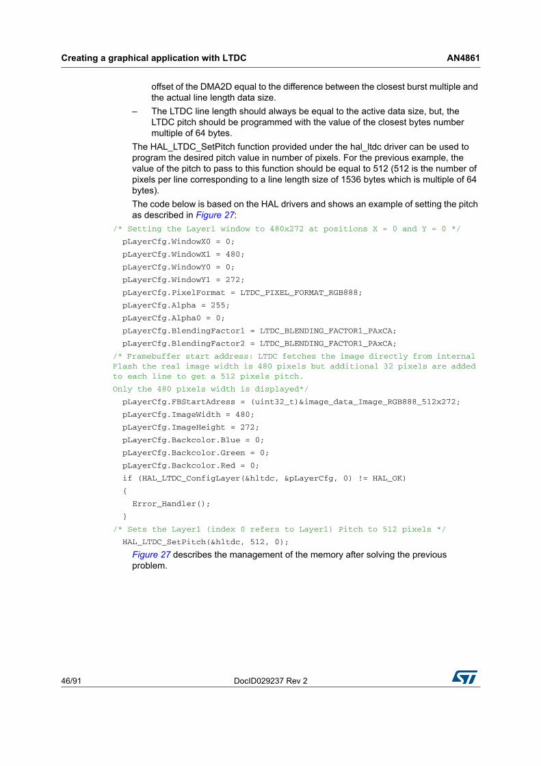
Creating a graphical application with LTDC AN4861
46/91 DocID029237 Rev 2
offset of the DMA2D equal to the difference between the closest burst multiple and the actual line length data size.
– The LTDC line length should always be equal to the active data size, but, the LTDC pitch should be programmed with the value of the closest bytes number multiple of 64 bytes.
The HAL_LTDC_SetPitch function provided under the hal_ltdc driver can be used to program the desired pitch value in number of pixels. For the previous example, the value of the pitch to pass to this function should be equal to 512 (512 is the number of pixels per line corresponding to a line length size of 1536 bytes which is multiple of 64 bytes).
The code below is based on the HAL drivers and shows an example of setting the pitch as described in Figure 27:
/* Setting the Layer1 window to 480x272 at positions X = 0 and Y = 0 */
pLayerCfg.WindowX0 = 0;
pLayerCfg.WindowX1 = 480;
pLayerCfg.WindowY0 = 0;
pLayerCfg.WindowY1 = 272;
pLayerCfg.PixelFormat = LTDC_PIXEL_FORMAT_RGB888;
pLayerCfg.Alpha = 255;
pLayerCfg.Alpha0 = 0;
pLayerCfg.BlendingFactor1 = LTDC_BLENDING_FACTOR1_PAxCA;
pLayerCfg.BlendingFactor2 = LTDC_BLENDING_FACTOR1_PAxCA;
/* Framebuffer start address: LTDC fetches the image directly from internal Flash the real image width is 480 pixels but additional 32 pixels are added to each line to get a 512 pixels pitch.
Only the 480 pixels width is displayed*/
pLayerCfg.FBStartAdress = (uint32_t)&image_data_Image_RGB888_512x272;
pLayerCfg.ImageWidth = 480;
pLayerCfg.ImageHeight = 272;
pLayerCfg.Backcolor.Blue = 0;
pLayerCfg.Backcolor.Green = 0;
pLayerCfg.Backcolor.Red = 0;
if (HAL_LTDC_ConfigLayer(&hltdc, &pLayerCfg, 0) != HAL_OK)
{
Error_Handler();
}
/* Sets the Layer1 (index 0 refers to Layer1) Pitch to 512 pixels */
HAL_LTDC_SetPitch(&hltdc, 512, 0);
Figure 27 describes the management of the memory after solving the previous problem.

DocID029237 Rev 2 47/91
AN4861 Creating a graphical application with LTDC
89
Figure 27. Adding dummy bytes to make the line width multiple of 64 bytes
4.5.3 Optimizing the LTDC framebuffer fetching from SDRAM
Making random access into a bank generates some precharge cycles which increase the SDRAM latency seen by the LTDC. As the LTDC is performing sequential accesses, it's important that no other masters are doing access into the same SDRAM bank.
The external SDRAM is composed of multiple banks. Given that making random accesses on a bank generates some precharge and activates some cycles, the framebuffer must be placed in an independent bank accessed only by the LTDC. This action reduces the external memory latency and leads to a higher throughput. As a consequence, when double framebuffer technique is used, it is recommended to have these buffers in two separate banks.
This can be done by storing the frontbuffer in the first address of the SDRAM and addressing the backbuffer by adding an offset with the size of one bank. Refer to Figure 28.

Creating a graphical application with LTDC AN4861
48/91 DocID029237 Rev 2
Figure 28. Placing the two buffers in independent SDRAM banks
For instance, when the SDRAM bank size is equal to 4 MByte, the following line code can be used:
/* Framebuffer addresses within external SDRAM */
/* Frontbuffer in bank 1 of SDRAM memory */
uint32_t FrontBuffer = LCD_FB_START_ADRESS;
/* Backbuffer in the bank 2 of SDRAM memory */
uint32_t BackBuffer = LCD_FB_START_ADRESS + 1024 * 1024 * 4;
SDRAM RBURST
Another interesting feature allowing to optimize the reading performances from the SDRAM is the use of RBURST.
The SDRAM controller adds a cacheable read FIFO with a depth of 6 32-bit lines. The read FIFO is used when the read burst is enabled and allows to anticipate the next read accesses during CAS latencies.
4.5.4 Framebuffer content update during BLANKING period
A way to optimize graphic performance (especially when the performance bottleneck is the framebuffer memory bandwidth), is to update the framebuffer content during the blanking period. Since in this period the LTDC is not fetching any pixel data from the framebuffer, the bus bandwidth is relaxed and it allows the update of the framebuffer.
4.6 Special recommendations for Cortex®-M7 (STM32F7 Series)
This section illustrates some recommendations for the STM32F7 Series embedding the Cortex®-M7 CPU. These recommendations are specific to the Cortex®-M7 since it has the following particularities compared to the Cortex®-M4 CPU:
• The Cortex®-M7 does some speculative read accesses to normal memory regions. These speculative read accesses could cause high latency or system errors when performed on external memories like SDRAM or Quad-SPI. This impacts AHB masters (such as LTDC) accessing the FMC or Quad-SPI and particularly decreases graphical

DocID029237 Rev 2 49/91
AN4861 Creating a graphical application with LTDC
89
performances and may lead to system errors (if the LTDC framebuffer is located in external memory and/or if the Quad-SPI memory is used for graphics).
• The Cortex®-M7 CPU embeds an L1-Cache (see Figure 10). Some graphic issues may be encountered due to unsuitable cache settings; bad graphic visual effects may occur if cache maintenance is not properly performed. If the suitable cache maintenance method is not used, graphical performances may be impacted.
4.6.1 Disable FMC bank1 if not used
After reset, the FMC bank1 is always enabled to allow boot into external memories. Since the Cortex®-M7 is doing some speculations, it can generate a speculative read access to the first FMC bank.
The default FMC configuration being very slow, this speculative access blocks the access to the FMC by other AHB masters for a very long time, leading to underrun on the LTDC side.
To prevent this CPU speculative read accesses on the FMC bank1, it is recommended to disable it when it is not used. This can be done by resetting the MBKEN Bit in FMC_BCR1 register which is by default enabled after reset.
To disable the FMC Bank1, the user can use the following code:
/* Disabling FMC Bank1: After reset FMC_BCR1 = 0x000030DB
where MBKEN = 1b meaning that FMC_Bank1 is enabled
and MTYP[1:0]= 10 meaning that memory type is set to NOR Flash/OneNAND Flash*/
FMC_Bank1->BTCR[0] = 0x000030D2;
For more details on FMC configuration refer to the relevant STM32 reference manual.
4.6.2 Configure the memory protection unit (MPU)
This section defines the STM32F7 Series system memory attributes and the basic MPU concepts. It also describes how to configure the MPU in order to prevent graphical performance issues related to the Cortex®-M7 speculative read accesses and cache maintenance.
Note: This section is only describing some necessary basic MPU concepts needed for configuration. For further details on MPU and cache, refer to the following documents:
- AN4838 application note “Managing memory protection unit (MPU) in STM32 MCUs”
- AN4839 application note “Level 1 cache on STM32F7 Series”
- STM32F7 Series Cortex®-M7 processor programming manual (PM0253)
- ARM Cortex®-M7 technical reference manual.

Creating a graphical application with LTDC AN4861
50/91 DocID029237 Rev 2
MPU attributes configuration
In order to prevent graphic performance issues related to the Cortex®-M7 speculative read accesses, the user should review all the memory map of the application and configure the MPU according to the hardware. So, the user has to set the following configurations:
• Define the framebuffer MPU region and the other application MPU regions.
• MPU must be configured according to the size of the memory used by the application.
• The MPU attributes of the unused regions must be configured to strongly ordered execute never (XN). For example, for the Quad-SPI, if an 8 MByte memory is connected, the remaining 248 MByte unused space (from a total 256 MByte addressable space) must be set to strongly ordered XN. See example in Section 6.2.7.
• Prevent the Coretx-M7 speculative read accesses to the external SDRAM/SRAM (if the FMC swap is enabled, see Figure 29), to do it the SDRAM/SRAM MPU region must be set to execute never (XN).
• If the Cortex®-M7 CPU is used for framebuffer processing (writing to SDRAM/SRAM), the framebuffer region MPU attribute should be set to normal cacheable with read and write access permission.
Note: The framebuffer MPU region attribute should be set to execute never since it is only dedicated for graphical content creation.
Figure 29 describes the STM32F7’s FMC banks and Quad-SPI MPU memory attributes at default system memory map

DocID029237 Rev 2 51/91
AN4861 Creating a graphical application with LTDC
89
Figure 29. FMC SDRAM and NOR/PSRAM memory swap at default system memory map (MPU disabled)
MPU and Cache policy configuration
The use of Cortex®-M7 cache allows to boost system and graphic performances. This performance gain is especially seen when CPU is accessing external memories such as SDRAM or Quad-SPI.
In a graphical application, when the CPU is used for framebuffer processing, it is recommended to use the cache especially if the framebuffer is located in an external memory like SDRAM or SRAM. In that case user should consider the following points when using the cache:
• MPU memory region cacheability
As previously illustrated in Figure 29, in the default system memory region MPU attributes, some system memory regions are normal cacheable while others are device non-cacheable.
When the CPU is used for framebuffer processing, the user should change the framebuffer region MPU attribute to normal cacheable (or do an FMC swap, see Figure 29).

Creating a graphical application with LTDC AN4861
52/91 DocID029237 Rev 2
• Cache maintenance and data coherency: visual impact of WBWA without cache maintenance operation
The data coherency issue is often encountered when performing framebuffer processing using a Cortex®-M7 CPU with L1-cache enabled and a WBWA cache policy. This issue occurs when multiple masters such as Cortex®-M7 and LTDC are sharing the same region (framebuffer) and the cache maintenance is not performed. When the CPU is processing the framebuffer (writes to framebuffer) and if the framebuffer region has a write-back cache policy, the processed result (image to be displayed) is not seen on the framebuffer (may be SRAM or SDRAM), and then it is not displayed.
To avoid this issue, the user should use one of the following methods:
– Configure the framebuffer region cache attribute to write-through (WT), in that case each write operation is performed on the cache and on the framebuffer.
– Configure the framebuffer region cache attribute to write back write allocate (WBWA) and perform the cache maintenance by software.
Write-through is safer for data coherency but may impact graphic performances.
• Cache maintenance may impact graphic performances
The user should use the suitable cache policy matching his application. Each method has its cons and pros. So the user should consider the following particularities for each method:
– Write-through: is very simple to manage (no need to perform cache maintenance by software) and safer for data coherency but it generates a lot of single write operations to the framebuffer which may impact LTDC accesses.
Note: The user should also consider that cache maintenance may impact graphic performances even when the CPU is not used for framebuffer processing. Thus, in some applications the CPU is accessing to the external SDRAM or SRAM for purposes other than graphics with cache enabled. In that case, cache maintenance may impact the LTDC accesses.
– Write back write allocate: it is more suitable to use WBWA and software routine and synchronize the cache maintenance operation with the LTDC during blanking. This allows to create additional bandwidth on the framebuffer memory (SRAM or SDRAM). The cache maintenance operation should be performed by software after writing data to the framebuffer memory region; this is done by forcing a D-cache clean operation using the CMSIS function SCB_CleanDCache(). So all the dirty lines in the cache are written back to the framebuffer.
MPU configuration example
An example of MPU configuration is described in Section 6.2.7, showing how to set the framebuffer MPU attribute when the CPU is used (with cache enabled) for graphical operations. The described example is created for the STM32F746G-DISCO board hardware configuration where the external SDRAM is used for framebuffer and the external QSPI Flash memory is containing the graphic primitives.

DocID029237 Rev 2 53/91
AN4861 Creating a graphical application with LTDC
89
4.7 LTDC peripheral configuration
This section describes the steps needed to configure the LTDC peripheral.
Note: It is recommended to reset the LTDC peripheral before starting the configuration and also it is recommended to guarantee that the peripheral is in reset state. The LTDC can be reset by setting the corresponding bit in the RCC_APB2RSTR register, which resets the three clock domains.
4.7.1 Display panel connection
The LTDC hardware interface provides eight bits per color bus, and fits perfectly for RGB888 true color panels. The LTDC hardware interface provides also timing signals: LCD_HSYNC, LCD_VSYNC, LCD_DE and LCD_CLK.
The LTDC GPIOs should be configured to the correspondent alternate function. For more details on LTDC alternate functions availability versus GPIOs, refer to the alternate function mapping table in the relevant datasheet.
Note: All GPIOs have to be configured in very high-speed mode.
Connecting lower palette display panels
For display panels with a lower color palette (such as RGB666 and RGB565), the bus connection should be done with the most significant bits of the data signals. Figure 30 shows an example of connecting an RGB666 display panel.
Figure 30. Connecting an RGB666 display panel

Creating a graphical application with LTDC AN4861
54/91 DocID029237 Rev 2
GPIOs configuration using STM32CubeMX tool
To connect a display panel to an STM32 MCU, the user should configure the GPIOs to be used for interfacing.
Using the STM32CubeMX tool is a very simple, easy and rapid way to configure the LTDC peripheral and its GPIOs since it allows to generate a project with a preconfigured LTDC.
Section Section 6.2.3: LTDC GPIOs configuration provides a guide on how to configure the LTDC GPIOs.
Configuration of specific pins of a display module
Some display modules may need other signals to be fully functional. The user can use GPIOs and some peripherals to control these signals.
An example of using GPIOs to control the display enable pin (LCD_DISP) on a display panel is described in section Section 6.2.3: LTDC GPIOs configuration.
Enabling LTDC interrupts
To be able to use the LTDC interrupts, the user should enable the LTDC global interrupts on the NVIC side. Then, each interrupt is enabled separately by enabling its corresponding enable bit. The LTDC interrupt-enable bits are available in the LTDC_IER register described in Table 7: LTDC interrupts summary.
Note: The FIFO underrun and transfer error interrupts are enabled in the hal_ltdc driver HAL_LTDC_Init() function
An example of enabling LTDC interrupts using STM32CubeMX is described in Section 6.2.3: LTDC GPIOs configuration.
4.7.2 LTDC clocks and timings configuration
This section describes the steps needed to configure the LTDC clock and timings respecting the display specifications. It also provides a configuration example for the ROCKTECH (RK043FN48H) display embedded on the STM32F746G-DISCO board.
System clock configuration
It is recommended to use the highest system clock to get the best graphic performances. This recommendation applies also for the external memory framebuffer. So if an external memory is used for the framebuffer, the highest allowed clock speed should be used to get the best memory bandwidth.
For instance for the STM32F4x9 microcontrollers the maximum system speed is 180 MHz, so if an external SDRAM is connected to the FMC the maximum SDRAM clock is 90 MHz (HCLK/2).
For the STM32F7 Series, the maximum system speed is 216 MHz but with this speed and HCLK/2 prescaler the SDRAM speed exceeds the maximum allowed speed (see product”s datasheet for more details). So to get the maximum SDRAM, it is recommended to configure HCLK to 200 MHz, then the SDRAM speed is set to 100 MHz.
The clock configuration providing the highest performances is:
• STM32F4x9 devices: HCLK @ 180 MHz and SDRAM @ 90 MHz.
• STM32F7 Series: HCLK @ 200 MHz and SDRAM @ 100 MHz.

DocID029237 Rev 2 55/91
AN4861 Creating a graphical application with LTDC
89
An example of LTDC configuration using STM32CubeMX is described in Section 6.2.4: LTDC peripheral configuration.
Pixel clock and timings configuration
At this stage of the graphical application development, the user should have already checked and confirmed that the desired display size and color depth are compatible with the hardware configuration. Therefore, the pixel clock to be configured should be already known, either extracted from display datasheet or calculated (see Section 4.2.2: Checking display compatibility considering the memory bandwidth requirements).
Example: LTDC timings configuration for ROCKTECH RK043FN48H display embedded on the STM32F746G-DISCO board
At first, the user should extract the timing parameters from the display’s datasheet (see Table 14). It is recommended to use typical display timings.
Table 14. LCD-TFT timings extracted from ROCKTECH RK043FN48H datasheet (1)
1. The gray cells highlight the values used in the example presented below.
Item Symbol Min. Typ. Max. Unit
DCLK frequency Fclk 5 9 12 MHz
DCLK period Tclk 83 110 200 ns
Hsync
Period time Th 490 531 605 DCLK
Display period Thdisp - 480 - DCLK
Back porch Thbp 8 43 - DCLK
Front porch Thfp 2 8 - DCLK
Pulse width Thw 1 - - DCLK
Vsync
Period time Tv 275 288 335 H
Display period Tvdisp - 272 - H
Back porch Tvbp 2 12 - H
Front porch Tvfp 1 4 - H
Pulse width Tvw 1 10 - H

Creating a graphical application with LTDC AN4861
56/91 DocID029237 Rev 2
Based on Table 14, the extracted timing parameters are:
– Display period (active width) = 480 pixels
– Back porch HBP = 43 pixels
– Front porch HFP = 8 pixels
– Pulse width HSYNC = 1 pixel (minimum value)
– Display period (active height) = 272 pixels
– Vertical back porch VBP = 12 pixels
– Front porch VFP = 4 pixels
– Pulse width VSYNC = 10 pixel
Program timing parameters: once that the timing parameters are extracted, they are used to program the LTDC timing registers, Table 15 summarizes all the parameters to be programmed.
Timing parameters configuration with STM32CubeMX: it is very easy to program the timing parameters using STM32CubeMX, the user should simply fill the extracted parameters in the LTDC configuration window (see section Section 6.2.4: LTDC peripheral configuration).
Pixel clock configuration with STM32CubeMX: the pixel clock is calculated with a 60 Hz refresh rate as shown below:
LCD_CLK = TOTALW x TOTALH x refresh rate
Based on Table 15, TOTALW = 531 and TOTALH = 297.
And for this example:
LCD_CLK = 531 x 297 x 60 = 9.5 MHz
Refer to the LTDC pixel clock configuration STM32CubeMX example in Section 6.2.4.
LTDC control signals polarity configuration
The LTDC control signals (HSYNC, VSYNC, DE and LCD_CLK) polarities must be configured respecting the display specifications. The user should note that only the DE control signal should be inverted versus the DE polarity indicated in the display datasheet. The other control signals should be configured exactly like the display datasheet.
Table 15. Programming LTDC timing registers
RegisterValue to be
programmed
LTDC_SSCRHSW[11:0] HSYNC Width - 1 0
VSH[11:0] VSYNC Height - 1 9
LTDC_BPCRAHBP[11:0] HSYNC Width + HBP - 1 43
AVBP[10:0] VSYNC Height + VBP - 1 21
LTDC_AWCRAAW[11:0] HSYNC Width + HBP + Active Width - 1 523
AAH[10:0] VSYNC Height + BVBP + Active Height - 1 293
LTDC_TWCRTOTALW[11:0] HSYNC Width + HBP + Active Width + HFP - 1 531
TOTALH[10:0] VSYNC Height+ BVBP + Active Height + VFP - 1 297

DocID029237 Rev 2 57/91
AN4861 Creating a graphical application with LTDC
89
4.7.3 LTDC layer(s) configuration
This section describes the needed steps to configure the LTDC layer(s) respecting the display size and the color depth.
As previously stated in Section 3.3.2 the LTDC features two independently configurable layers, where the user can enable either one or the two layers. By default both layers are disabled so only the configured background color is displayed (the default color is black).
The user can display layer 1 + background or display layer 1 + layer 2 + background.
Display only the background
If no layer has been enabled, only the background is displayed. If the background color is not configured, the default background black color is displayed (LTDC_BCCR = 0x00000000).
To set a blue background color the LTDC_BCCR register should be set to 0x000000FF.
Layer parameters configuration
Once that the LTDC GPIOs, clocks and timings are properly set, the user should configure the following LTDC layer parameters. Each LTDC layer has its own parameters so it should be configured separately.
• Window size and position
• Pixel input format
• Framebuffer start address
• Framebuffer size (image width and image height) and pitch
• Layer default color in ARGB8888 format
• Layer constant alpha for blending
• Layer blending factor1 and factor2
An example of LTDC layer parameters configuration using STM32CubeMX is described in Section : LTDC Layer parameters configuration on page 75.
Note: All layer parameters can be modified on the fly except for the CLUT. The new configuration has to be either reloaded immediately or during vertical blanking period by configuring the LTDC_SRCR register.
4.7.4 Display panel configuration
Some displays require to be configured using serial communication interfaces such as I2C or SPI.
For instance the STM32F429I-DISCO is embedding the ILI9341 display module which is initialized through the SPI interface.
A dedicated driver for this display module (ili9341.c) including initialization and configuration commands is available in the STM32Cube firmware package under:
STM32Cube_FW_F4_Vx.xx.x\Drivers\BSP\Components\ili9341
An example of display initialization sequence based on the ili9341_Init() function is included in the STM32Cube examples for the STM32F429I-Discovery board under
STM32Cube_FW_F4_Vx.xx.x\Projects\STM32F429I-Discovery\ Examples\LTDC\LTDC_Display_2Layers

Creating a graphical application with LTDC AN4861
58/91 DocID029237 Rev 2
4.8 Storing graphic primitives
Graphic primitives are basic elements (such as images or fonts) which can combined to build the framebuffer content that is displayed.
Static data should be placed in a non-volatile memory. When the amount of data to store is relatively low, the internal FLASH memory can be used. Otherwise, graphical contents should be placed in external memories.
The STM32 microcontrollers offer parallel (FMC) or serial (QSPI) interface for external NOR Flashes (see Table 3).
To build the framebuffer content, the DMA2D can directly read graphic primitives form a parallel NOR Flash or a Quad-SPI Flash.
Refer to the application note Quad-SPI (QSPI) interface on STM32 microcontrollers (AN4760) for more details on storing graphic content on QSPI memory.
4.8.1 Converting images to C files
To add graphic primitives to a user project, they should be converted to C or header files. In order to do that, the user can use some specific tools allowing to generate C or *.h files.
Warning: The user must convert images to C files respecting the configured pixel input format described in Section : Pixel input format on page 27. Some tools may generate C or *.h files with red and blue colors swapped. To avoid this issue (displaying an image with red and blue swapped), the user can use the LCD image converter tool.
The LCD image converter is a very customizable free tool allowing to convert images to C files and offering the possibility to generate the C file in the desired format. An example is described in Section 6.2.5: Displaying an image from the internal Flash.
4.9 Hardware considerations
This section provides some hardware considerations for a graphic application. In general two important hardware interfaces should be designed carefully: the LTDC interface and the external memory interface (used for framebuffer) such as FMC_SDRAM or FMC_SRAM.
LTDC parallel interface
When the pixel clock is below 40 MHz (SVGA), a simple 3.3 V signaling can be used.
It is possible to reach 83 MHz with a parallel RGB if the load and the wire length are reduced (for example to interface on the same PCB with on-board an LVDS transciver or HDMI transceiver).
It is recommended to configure the LTDC GPIOs at the maximum operating speed OSPEEDRy[1:0] = 11b. Refer to the relevant STM32 reference manual for a description of the GPIOx_SPEEDR GPIO port output speed register.

DocID029237 Rev 2 59/91
AN4861 Creating a graphical application with LTDC
89
FMC SDRAM/SRAM interface
When using an external SRAM or SDRAM memory for a framebuffer, the FMC-SDRAM and the FMC-SRAM interfaces speed depend on many factors including the board layout and the pad speed. A good PCB design enables to reach the maximum pixel clock described in Table 10 and Table 11.
The layout should be as good as possible in order to get the best performances. To get more information on PCB routing guidelines, refer to the following application notes available on the STMicroelectronics website:
• Section “Flexible memory controller (FMC) interface” of application note Getting started with STM32F7 Series MCU hardware development (AN4661)
• Section “Flexible memory controller (FMC) interface” of application note Getting started with STM32F4xxxx MCU hardware development (AN4488)

Saving power consumption AN4861
60/91 DocID029237 Rev 2
5 Saving power consumption
When an application is in idle state and displaying only a screen saver, it is important to drive the STM32 chip in sleep mode to reduce the power consumption. In sleep mode all peripherals can be enabled (FMC-SDRAM and LTDC for instance) while the CPU is stopped.
External memories such as SDRAM or QSPI FLASH can be driven in low-power modes whenever it is needed in order to avoid the waste of power.
If the application is in low-power state but requires to display graphics, the LTDC can be kept active and the SDRAM can be put in self-refresh mode (in order to save power). If the application is set in power-down mode, it saves even more power.
The display can also be disabled or put in low-power mode if it is not needed when running the application.

DocID029237 Rev 2 61/91
AN4861 LTDC application examples
89
6 LTDC application examples
This section provides:
• Some graphic implementation examples considering the resources requirements
• An example on how to create a basic graphical application
• A summary of STM32 reference boards with embedding LTDC and featuring an on-board LCD-TFT panel
6.1 Implementation examples and resources requirements
This section provides some graphic implementation examples detailing the hardware resources requirements.
6.1.1 Single chip MCU
Thanks to their integrated SRAM, the STM32 MCUs can be used for graphic applications without the need of an external SDRAM/SRAM memory for framebuffer. Also, thanks to their high size internal Flash (up to 2 MByte), the user can use them to store graphic primitives. The use of internal memories allows to reduce the used pins, ease the PCB design and make cost savings.
In order to use a single chip MCU for a graphical application, the user can use the following hardware configuration:
• Internal Flash up to 2 MByte: storing user application code and graphic primitives.
• The framebuffer should be located in the internal SRAM, so depending on the internal SRAM size for each STM32 MCU, the user can interface with a corresponding display size and color depth as illustrated below:
– STM32F7x7 line: use SRAM1 (368 Kbyte) to support resolutions 400 x 400 16 bpp (313 Kbyte) or 480 x 272 16 bpp (255 Kbyte).
– STM32F7x6 line: use SRAM1 (240 Kbyte) to support 320 x 320 resolution with 16 bpp (200 Kbyte).
– STM32F469/F479 line: use SRAM1 (160 Kbyte) to support 320 x 240 resolution with 16 bpp (154 Kbyte).
– STM32F429/F439 line: use SRAM1 (112 Kbyte) to support 320 x 240 resolution with 8 bpp (75 Kbyte).
– STM32 MCU packages: LQFP100 or TFBGA100
Figure 31 illustrates a graphic implementation example where only a single chip with no external memories is used.

LTDC application examples AN4861
62/91 DocID029237 Rev 2
Figure 31. Low-end graphic implementation example
6.1.2 MCU with external memory
In order to interface with higher resolution displays, an external memory connected to the FMC is needed for framebuffer. An external QSPI Flash memory can be used to store graphic primitives.
For mid-end or high-end graphical applications, the user can use the following hardware configuration example:
• External QSPI Flash memory with up to 256 MByte addressable memory-mapped is used for storing graphic primitives.
• External SDRAM 32-bit memory used for framebuffer.
• STM32 MCU packages: UFBGA169, UFBGA176, LQFP176, LQFP208, TFBGA216, WLCSP168 and WLCSP180.
Figure 32 illustrates a graphic implementation example where two external memories are connected to a STM32 MCU, one for the framebuffer and the other for graphic primitives.

DocID029237 Rev 2 63/91
AN4861 LTDC application examples
89
Figure 32. High-end graphic implementation example
Table 16 summarizes an example of graphic implementations in different STM32 hardware configurations.
Table 16. Example of graphic implantations with STM32 in different hardware configurations
Variant Display sizeColor depth
External memory - SDRAM
Display interface
STM32 package(1)
1. Package availability of STM32 MCUs embedding LTDC is summarized in Table 13.
Hig-end
1280 x 72016 bpp
32-bit RGB888
UFBGA176 TFBGA216/UFBGA169/
LQFP176/LQFP208
WLCSP180/WLCSP168
1024 x 768
1600 x 27224 bpp
800 x 600
Mid-end
800 x 600 16 bpp
16-bit RGB666 LQFP144/WLCSP143800 x 480
24 bpp640 x 480
400 x 400(2)
Low-end
400 x 400(2)
16 bpp No RGB666 LQFP100/TFBGA100480 x 272
320 x 320(2)
320 x 240

LTDC application examples AN4861
64/91 DocID029237 Rev 2
6.2 Example: creating a basic graphical application
This section provides an example based on the STM32F746G-DISCO board describing the steps required to create a basic graphic application.
6.2.1 Hardware description
The hardware resources embedded on the STM32F746G-DISCO board are used in this example. Figure 33 describes the graphic hardware resources to be used:
Figure 33. Graphic hardware configuration in the STM32F746G-DISCO
1. The pink arrow shows the pixel data path to the display.
The STM32F746G-DISCO board embeds a parallel true color RGB888 LCD-TFT panel with a 480 x 272 resolution.
For more details on the STM32F746G-DISCO board, please refer to user manual Discovery kit for STM32F7 Series with STM32F746NG MCU (UM1907) available on the ST Microelectronics website.
Figure 34 shows the ROCKTECH RK043FN48H true color panel (RGB888) connected to the STM32F746 MCU.
2. 400x400 and 320 x 320 are specific display resolutions commonly used for smartwatches.

DocID029237 Rev 2 65/91
AN4861 LTDC application examples
89
Figure 34. LCD-TFT connection in the STM32F746G-DISCO board
As shown in Figure 34, the display module is connected to the MCU through two different pin categories:
• LTDC interface pins:
– 24-bit RGB interface.
– Timing signals: LCD_HSYNC, LCD_VSYNC, LCD_DE and LCD_CLK.
• Other specific pins:
– LCD_DISP to enable/disable display standby mode.
– INT interrupt line: allows the touch sensor to generate interrupts.
– I2C interface to control the touch sensor.
– LCD_RST reset pin allowing to reset the LCD-TFT, it is connected to the global MCU reset pin (NRST).
– LCD_BL_A and LCD_BL_K pins for LED backlight control: the backlight is controlled by the STLD40DPUR circuit.
Backlight Controller: the STLD40DPUR circuit described in Figure 35 is a boost converter that operates from 3.0 V to 5.5 V. It can provide an output voltage as high as 37 V and can drive up to ten white LEDs in series. Refer to the STLD40D datasheet for more information on the backlight controller.
The high level on the LCD_BL_CTRL (PK3) signal lights the backlight on, while the low level switches it off.
Note: It is possible to change the display brightness (dim the backlight intensity) by applying a low-frequency (1 to 10 kHz) PWM signal to the EN pin 7 of the STLD40D circuit. This action needs a rework since there is no timer PWM output alternate function available on the PK3 pin, so user should remove the R81 resistance and connect another GPIO pin with the PWM output alternate function.
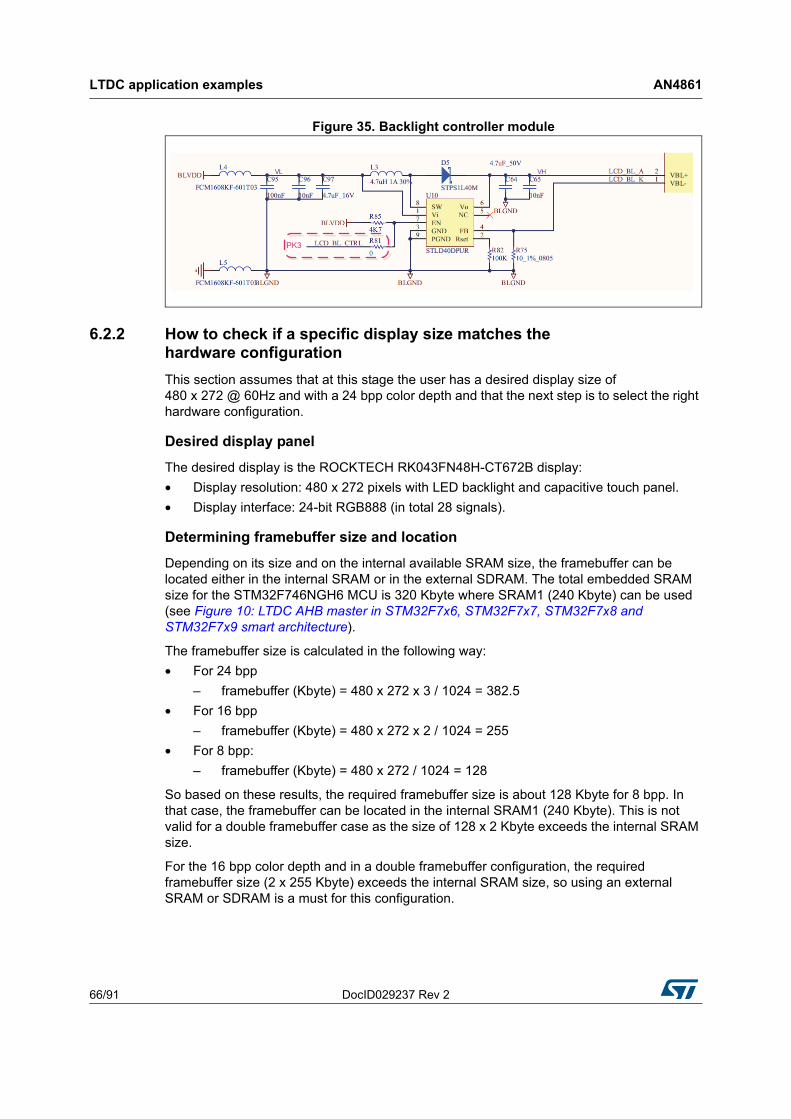
LTDC application examples AN4861
66/91 DocID029237 Rev 2
Figure 35. Backlight controller module
6.2.2 How to check if a specific display size matches the hardware configuration
This section assumes that at this stage the user has a desired display size of 480 x 272 @ 60Hz and with a 24 bpp color depth and that the next step is to select the right hardware configuration.
Desired display panel
The desired display is the ROCKTECH RK043FN48H-CT672B display:
• Display resolution: 480 x 272 pixels with LED backlight and capacitive touch panel.
• Display interface: 24-bit RGB888 (in total 28 signals).
Determining framebuffer size and location
Depending on its size and on the internal available SRAM size, the framebuffer can be located either in the internal SRAM or in the external SDRAM. The total embedded SRAM size for the STM32F746NGH6 MCU is 320 Kbyte where SRAM1 (240 Kbyte) can be used (see Figure 10: LTDC AHB master in STM32F7x6, STM32F7x7, STM32F7x8 and STM32F7x9 smart architecture).
The framebuffer size is calculated in the following way:
• For 24 bpp
– framebuffer (Kbyte) = 480 x 272 x 3 / 1024 = 382.5
• For 16 bpp
– framebuffer (Kbyte) = 480 x 272 x 2 / 1024 = 255
• For 8 bpp:
– framebuffer (Kbyte) = 480 x 272 / 1024 = 128
So based on these results, the required framebuffer size is about 128 Kbyte for 8 bpp. In that case, the framebuffer can be located in the internal SRAM1 (240 Kbyte). This is not valid for a double framebuffer case as the size of 128 x 2 Kbyte exceeds the internal SRAM size.
For the 16 bpp color depth and in a double framebuffer configuration, the required framebuffer size (2 x 255 Kbyte) exceeds the internal SRAM size, so using an external SRAM or SDRAM is a must for this configuration.

DocID029237 Rev 2 67/91
AN4861 LTDC application examples
89
For the 24 bpp color depth and in a double framebuffer configuration, the required framebuffer size exceeds the internal SRAM size (2 x 382.5 Kbyte), so using an external SRAM or SDRAM is a must for this configuration.
The next step is to check if the SDRAM 16-bit bus width can sustain the desired resolution and color depth.
Check if a 480 x 272 resolution with 24 bpp fits the SDRAM 16-bit configuration
At this stage the user should have decided to use an external SDRAM but still has to check if the SDRAM 16-bit bus width (actual hardware implementation in the discovery board) matches the 480 x 272 @ 60 Hz display size and 24 bpp color depth.
In order to conclude if such hardware configuration can support the desired display size and color depth or not, the user should first compute the pixel clock.
The computed LCD_CLK is about 9.5 MHz (for computing pixel clock refer to Section 6.2.3: LTDC GPIOs configuration.
Then the user should check based on the following parameters if the computed pixel clock is not higher than the maximum LCD_CLK indicated in Table 11.
– Number of used LTDC layers: in this example only one layer is used.
– System clock speed HCLK and framebuffer memory speed: HCLK @ 200 MHz and SDRAM @ 100 MHz.
– External framebuffer memory bus width SDRAM 16-bit.
– Number of AHB masters accessing concurrently to external SDRAM: 2 masters (DMA2D and LTDC).
Referring to the pixel clock Table 11 in the “LTDC + DMA2D” column and one layer row, the pixel clock can reach 34 MHz for SDRAM of 16-bit.
So the SDRAM 16-bit bus width is quite enough to sustain a 480 x 272 @ 60 Hz resolution (LCD_CLK = 9.5 MHz) with 24 bpp color depth.
6.2.3 LTDC GPIOs configuration
As shown on Figure 34, the ROCKTECH RK043FN48H display is connected to the STM32F746xx using a parallel RGB888 of 24 bits.
LTDC RGB interface pins configuration
Once that the STM32CubeMX project is created, in the Pinout tab choose one from the listed hardware configurations. Figure 36 shows how to select the RGB888 hardware configuration with the STM32CubeMX.
The user can also configure all the GPIOs by setting the right alternate function for each GPIO one by one.

LTDC application examples AN4861
68/91 DocID029237 Rev 2
Figure 36. STM32CubeMX: LTDC GPIOs configuration
If after selecting one hardware configuration (RGB888 as shown in Figure 36) the used GPIOs does not match with the display panel connection board, the user can change the desired GPIO and configure the alternate function directly on the pin. Figure 37 shows for instance how to configure manually a PJ7 pin to LTDC_G0 alternate function.
Figure 37. STM32CubeMX: PJ7 pin configuration to LTDC_G0 alternate function
The used pins are highlighted in green once that all the LTDC interface GPIOs are correctly configured.
Once that all the LTDC GPIOs pins are configured, the user should set their speed to very high.
To set the GPIOs speed using STM32CubeMX, select the configuration tab then click on the LTDC button as shown in Figure 38.

DocID029237 Rev 2 69/91
AN4861 LTDC application examples
89
Figure 38. STM32CubeMX: LTDC configuration
In the LTDC configuration window described in Figure 39, select all the LTDC pins then set the maximum output speed to very high.
Figure 39. STM32CubeMX: LTDC GPIOs output speed configuration
Specific pins configuration of the display module
Once that all the LTDC interface pins are correctly configured respecting the LCD-TFT panel connection, the user should configure the other specific pins connected to the display (LCD_DISP, INT pin and I2C interface)
The LCD_DISP pin (PI12 pin) has to be configured as an output push pull with high level in order to enable the display, otherwise the display stays in standby mode.

LTDC application examples AN4861
70/91 DocID029237 Rev 2
To configure the LCD_DISP pin in output mode with STM32CubeMX, in the pinout tab click on the PI12 pin then select GPIO_Output (see Figure 40).
Figure 40. STM32CubeMX: display enable pin (LCD_DISP) configuration
Then, the LDC_DISP (PI12) pin should be configured to high level, to do it, in the configuration tab click on GPIO button. Then in the pin configuration window set the GPIO output level to high as described in Figure 41.
Figure 41. STM32CubeMX: setting LCD_DISP pin output level to high

DocID029237 Rev 2 71/91
AN4861 LTDC application examples
89
Due to the R85 pull up resistance, the backlight is at its highest level by default if the LCD_BL_CTRL (PK3) pin is kept floating so there is no need to configure this pin.
Enabling LTDC interrupts
The FIFO underrun and transfer error interrupts are enabled in the hal_ltdc driver HAL_LTDC_Init() function. So the user should just enable the LTDC global interrupt on the NVIC side.
To enable the LTDC global interrupts using STM32CubeMX, select the configuration tab then click on the LTDC button as shown in Figure 38.
In the LTDC configuration window shown in Figure 42 select the NVIC settings tab, check the LTDC global interrupts then click on the OK button.
Figure 42. STM32CubeMX: enabling LTDC global and error interrupts
6.2.4 LTDC peripheral configuration
This section demonstrates how to configure LTDC clocks / timings and layer parameters using the STM32CubeMX tool.

LTDC application examples AN4861
72/91 DocID029237 Rev 2
LTDC Clocks and timings configuration
System clock configuration
In this example the system clock is configured as shown in Figure 44, and with below configuration:
– Use of internal HSI RC where main PLL is used as system source clock.
– HCLK @ 200 MHz so Cortex®-M7 and LTDC are both running @ 200 MHz.
Note: HCLK is set to 200 MHz but not 216 MHz, this is to set the SDRAM_FMC at its maximum speed of 100 MHz with HCLK/2 prescaler.
In order to configure the system clock using STM32CubeMX, select the clock configuration tab as shown in Figure 43.
Figure 43. STM32CubeMX: clock configuration tab
Then, to get the system clock HCLK @ 200 MHz, set the PLLs and the prescalers in the clock configuration tab as shown in the Figure 44.
Figure 44. STM32CubeMX: System clock configuration

DocID029237 Rev 2 73/91
AN4861 LTDC application examples
89
Pixel clock configuration
The LCD_CLK should be calculated using the parameters found in the display datasheet.
In order to do the calculation, the user should determine the total width and the total height.
The pixel clock is calculated with a 60 Hz refresh rate as shown below:
LCD_CLK = TOTALW x TOTALH x refresh rate (see extracted display timing parameters in Section 4.7.2: LTDC clocks and timings configuration)
LCD_CLK = 531 x 297 x 60 = 9.5 MHz
To configure the LTDC pixel clock to 9.5 MHz using STM32CubeMX, select the clock configuration tab then set the PLLSAI and the prescalers as shown in the Figure 45.
Figure 45. STM32CubeMX: LTDC pixel clock configuration
Timing parameters configuration
In order to configure the display timings using STM32CubeMX, the user should extract the timing parameters from the device’s datasheet. For this example, see an extract of ROCKTECH datasheet on Table 14. It is recommended to use the typical display timings.
In order to configure the display timing, the user must go to the configuration tab as indicated in Figure 38, and then click on the LTDC button.
In the LTDC configuration window, the user should select the Parameter Settings tab and fill in the timing values (refer to Figure 46).
LTDC control signals polarity configuration
Referring to the display datasheet, the HSYNC and VSYNC should be active low and the DE signal should be active high. As the DE signal is inverted in the output then it should be set to active low as well. The LCD_CLK signal should not be inverted.
Figure 46 shows both the control signal polarity configuration as well the LTDC configuration according to the ROCKTECH display datasheet.

LTDC application examples AN4861
74/91 DocID029237 Rev 2
Figure 46. STM32CubeMX: LTDC timing configuration

DocID029237 Rev 2 75/91
AN4861 LTDC application examples
89
LTDC Layer parameters configuration
At this stage all LTDC clocks and timings should have been set in the STM32CubeMX project.
The user should configure the LTDC layer1 parameters according to the display size and the color depth.
If needed, the user can also enable the layer2 by setting to “2 layers” the “Number of Layers” field in the LTDC configuration window shown in Figure 47.
To set the LTDC layer1 parameters using STM32CubeMX, the user must select the configuration tab then click on the LTDC button as shown in Figure 37.
In the LTDC configuration window shown in Figure 47 the user must select the Layer Settings tab, set the LTDC layer1 parameters and then click on the OK button.
At this step, the user can generate the project with the desired toolchain by clicking on “Project->Generate Code”

LTDC application examples AN4861
76/91 DocID029237 Rev 2
Figure 47. STM32CubeMX: LTDC Layer1 parameters setting
6.2.5 Displaying an image from the internal Flash
In order to ensure that the LTDC is properly configured respecting the display panel's specifications, it is important to display an image from the internal Flash.
To do it, the user should first convert the image to a C or a header file and add it to the project.
Converting the image to a header file using the LCD image converter tool
The user must generate the header file respecting the configured LTDC layer pixel input format RGB565 (see Section : Pixel input format on page 27 and Section 4.8: Storing graphic primitives on page 58).

DocID029237 Rev 2 77/91
AN4861 LTDC application examples
89
In this example the LCD-Image-Converter-20161012 tool is used (see Section 4.8 for more details on this tool).
To convert an image, the user must first run the LCD-Image-Converter tool, then in the home page shown in the Figure 48 click on “File->Open” then select the image file to be converted.
The used image size should be aligned with the LTDC layer1 configuration (480 x 272). If the used image size is not aligned with the LTDC layer1 configuration, the user can resize the image by going to Image->Resize or choose another image with the correct size.
For this example the used image size is 480 x 272 and it is showing the ST logo (see Figure 49).
Figure 48. LCD Image Converter: home page
The image is then displayed on the tool's home page as described in Figure 49.
To convert the image to a header file avoiding the red and blue swap issue explained in Section 4.8: Storing graphic primitives, the user should configure the tool to convert the image to a table of 32-bit words. To do it, in the home page menu click on Options->Conversion as shown in Figure 49.

LTDC application examples AN4861
78/91 DocID029237 Rev 2
Figure 49. LCD Image Converter: image project
In the Options window shown in Figure 50, select the “Image” tab then select the “RGB565 color” in the Preset field, then set the Block size field to 32-bit and click on OK button.
Note: The user can also convert the image to a table of bytes, but in that case he should swap the red and blue colors in the conversion window matrix tab.
Figure 50. LCD Image Converter: setting conversion options

DocID029237 Rev 2 79/91
AN4861 LTDC application examples
89
To generate the header file click on File->Convert. Then in the displayed window shown in Figure 51, set the file type to “C/C++ headers (*.h)”, then save the *.h file in include “\Inc” directory (same location as main.h file) by clicking on the Save button.
Figure 51. LCD Image Converter: generating the header file
The generated header file should be included in the main.c file. It includes a table of 32-bit words where each word represents two pixels.
In this header file, the user must comment the structure definition located just after the table and keep only the table definition as shown below:
/* Converted image: image_data_STLogo definition */
const uint32_t image_data_STLogo[65280] = {0xffffffff, 0xffffffff, ........};
Setting the LTDC framebuffer Layer1 start address to the internal Flash (image address in the Flash)
The generated project by STM32CubeMX should include in the main.c file the MX_LTDC_Init() function that allows to configure the LTDC peripheral.
In order to display the image, the user should set the LTDC Layer1 framebuffer start address to the address of the image in the internal Flash.
The MX_LTDC_Init() function is presented below with the framebuffer start address setting.
/* LTDC configuration function generated by STM32CubeMX tool */
static void MX_LTDC_Init(void)
{
LTDC_LayerCfgTypeDef pLayerCfg;
hltdc.Instance = LTDC;
/* LTDC control signals polarity setting */
hltdc.Init.HSPolarity = LTDC_HSPOLARITY_AL;
hltdc.Init.VSPolarity = LTDC_VSPOLARITY_AL;
hltdc.Init.DEPolarity = LTDC_DEPOLARITY_AL;
hltdc.Init.PCPolarity = LTDC_PCPOLARITY_IPC;
/* Timings configuration */
hltdc.Init.HorizontalSync = 0;
hltdc.Init.VerticalSync = 9;
hltdc.Init.AccumulatedHBP = 43;
hltdc.Init.AccumulatedVBP = 21;

LTDC application examples AN4861
80/91 DocID029237 Rev 2
hltdc.Init.AccumulatedActiveW = 523;
hltdc.Init.AccumulatedActiveH = 293;
hltdc.Init.TotalWidth = 531;
hltdc.Init.TotalHeigh = 297;
/* Background color */
hltdc.Init.Backcolor.Blue = 0;
hltdc.Init.Backcolor.Green = 0;
hltdc.Init.Backcolor.Red = 0x0;
if (HAL_LTDC_Init(&hltdc) != HAL_OK)
{
Error_Handler();
}
/* Layer1 Window size and position setting */
pLayerCfg.WindowX0 = 0;
pLayerCfg.WindowX1 = 480;
pLayerCfg.WindowY0 = 0;
pLayerCfg.WindowY1 = 272;
/* Layer1 Pixel Input Format setting */
pLayerCfg.PixelFormat = LTDC_PIXEL_FORMAT_RGB565;
/* Layer1 constant Alpha setting 100% opaque */
pLayerCfg.Alpha = 255;
/* Layer1 Blending factors setting */
pLayerCfg.BlendingFactor1 = LTDC_BLENDING_FACTOR1_PAxCA;
pLayerCfg.BlendingFactor2 = LTDC_BLENDING_FACTOR2_PAxCA;
/* User should set the framebuffer start address (can be 0xC0000000 if external SDRAM is used)*/
pLayerCfg.FBStartAdress = (uint32_t)&image_data_STLogo;
pLayerCfg.ImageWidth = 480;
pLayerCfg.ImageHeight = 272;
/* Layer1 Default color setting */
pLayerCfg.Alpha0 = 0;
pLayerCfg.Backcolor.Blue = 0;
pLayerCfg.Backcolor.Green = 0;
pLayerCfg.Backcolor.Red = 0;
if (HAL_LTDC_ConfigLayer(&hltdc, &pLayerCfg, 0) != HAL_OK)
{
Error_Handler();
}
}
Once the LTDC is correctly configured in the project, the user should build the project and then run it.

DocID029237 Rev 2 81/91
AN4861 LTDC application examples
89
6.2.6 FMC SDRAM configuration
The external SDRAM must be configured as it contains the LTDC framebuffer. To configure the FMC_SDRAM and the SDRAM memory device mounted on the STM32746G-Discovery board, the user can use either STM32CubeMX or use the existing BSP driver.
To configure the FMC_SDRAM using the BSP driver follow the steps described below:
1. Add the following files to the project: BSP stm32746g_discovery_sdram.c and stm32746g_discovery_sdram.h. Include the stm32f7xx_hal_sdram.h in the main.c file. Add the stm32f7xx_hal_sdram.c and stm32f7xx_ll_fmc.c HAL drivers to the project
2. Enable the SDRAM module in the stm32f7xx_hal_conf.h file by uncommenting the SDRAM module definition. Include the stm32f7xx_hal_sdram.h file in the main.c file.
3. Call the BSP_SDRAM_Init() function in the main() function.
6.2.7 MPU and cache configuration
As illustrated in Section 4.6, the MPU attributes should be correctly configured in order to prevent graphical performance issues related to the Cortex®-M7 speculative read accesses and cache maintenance.
This section describes an example of MPU attribute configuration with respect to the STM32F746G-DISCO board hardware configuration.
The MPU memory attributes can be easily configured with STM32CubeMX. A code example of MPU configuration generated using STM32CubeMX is described at the end of this section.
MPU configuration example: FMC_SDRAM
In this configuration example, the double framebuffer technique is used; the frontbuffer is placed in the SDRAM bank1 while the backbuffer is placed in the SDRAM bank2 with respect to the SDRAM bandwidth optimization described in Section 4.5.3: Optimizing the LTDC framebuffer fetching from SDRAM.
The following MPU regions are created (FMC without sawp):
• Region0: defines the SDRAM memory size 8 MByte
• Region1: defines the frontbuffer 256 Kbyte (16 bpp x 480 x 272), it overlaps region0
• Region2: defines the backbuffer 256 Kbyte (16 bpp x 480 x 272), it overlaps region0
Figure 52 illustrates the MPU configuration of the SDRAM region.

LTDC application examples AN4861
82/91 DocID029237 Rev 2
Figure 52. FMC SDRAM MPU configuration example
MPU configuration example: Quad-SPI in memory-mapped
This example shows how to configure the MPU for the Quad-SPI interface. The QSPI memory contains graphic primitives, it can be accessed by the Cortex®-M7, the DMA2D or the LTDC. For that, the Quad-SPI interface should be set to memory-mapped mode and the MPU regions must be configured as described below:
• Region3: defines the whole Quad-SPI addressable space, it must be set to strongly ordered to forbid any CPU speculative read access to that region.
• Region4: defines the real QSPI memory space reflecting the size of the memory which can be accessed by any master.
Figure 53 illustrates the MPU configuration of the Quad-SPI region.

DocID029237 Rev 2 83/91
AN4861 LTDC application examples
89
Figure 53. MPU configuration for Quad-SPI region
SDRAM and Quad-SPI MPU configuration example
The following code (generated by STM32CubeMX) shows how to set the MPU attributes for the FMC_SDRAM and Quad-SPI respecting the previously described configurations.
/* MPU Configuration */
void MPU_Config(void)
{
MPU_Region_InitTypeDef MPU_InitStruct;
/* Disables the MPU */
HAL_MPU_Disable();
/* Configure the MPU attributes for region 0 */
/* Configure the MPU attributes for SDRAM to normal memory*/
MPU_InitStruct.Enable = MPU_REGION_ENABLE;
MPU_InitStruct.Number = MPU_REGION_NUMBER0;
MPU_InitStruct.BaseAddress = 0xC0000000;
MPU_InitStruct.Size = MPU_REGION_SIZE_8MB;
MPU_InitStruct.SubRegionDisable = 0x0;
MPU_InitStruct.TypeExtField = MPU_TEX_LEVEL1;
MPU_InitStruct.AccessPermission = MPU_REGION_FULL_ACCESS;
MPU_InitStruct.DisableExec = MPU_INSTRUCTION_ACCESS_ENABLE;
MPU_InitStruct.IsShareable = MPU_ACCESS_NOT_SHAREABLE;
MPU_InitStruct.IsCacheable = MPU_ACCESS_CACHEABLE;
MPU_InitStruct.IsBufferable = MPU_ACCESS_BUFFERABLE;

LTDC application examples AN4861
84/91 DocID029237 Rev 2
HAL_MPU_ConfigRegion(&MPU_InitStruct);
/* Configure the MPU attributes for region 1 */
/* Configure the MPU attributes for the frontbuffer to normal memory*/
MPU_InitStruct.Enable = MPU_REGION_ENABLE;
MPU_InitStruct.Number = MPU_REGION_NUMBER1;
MPU_InitStruct.BaseAddress = 0xC0000000;
MPU_InitStruct.Size = MPU_REGION_SIZE_256KB;
MPU_InitStruct.SubRegionDisable = 0x0;
MPU_InitStruct.TypeExtField = MPU_TEX_LEVEL1;
MPU_InitStruct.AccessPermission = MPU_REGION_FULL_ACCESS;
MPU_InitStruct.DisableExec = MPU_INSTRUCTION_ACCESS_DISABLE;
MPU_InitStruct.IsShareable = MPU_ACCESS_NOT_SHAREABLE;
MPU_InitStruct.IsCacheable = MPU_ACCESS_CACHEABLE;
MPU_InitStruct.IsBufferable = MPU_ACCESS_BUFFERABLE;
HAL_MPU_ConfigRegion(&MPU_InitStruct);
/* Configure the MPU attributes for region 2 */
/* Configure the MPU attributes for the backbuffer to normal memory*/
MPU_InitStruct.Enable = MPU_REGION_ENABLE;
MPU_InitStruct.Number = MPU_REGION_NUMBER2;
MPU_InitStruct.BaseAddress = 0xC0200000;
MPU_InitStruct.Size = MPU_REGION_SIZE_256KB;
MPU_InitStruct.SubRegionDisable = 0x0;
MPU_InitStruct.TypeExtField = MPU_TEX_LEVEL1;
MPU_InitStruct.AccessPermission = MPU_REGION_FULL_ACCESS;
MPU_InitStruct.DisableExec = MPU_INSTRUCTION_ACCESS_DISABLE;
MPU_InitStruct.IsShareable = MPU_ACCESS_NOT_SHAREABLE;
MPU_InitStruct.IsCacheable = MPU_ACCESS_CACHEABLE;
MPU_InitStruct.IsBufferable = MPU_ACCESS_BUFFERABLE;
HAL_MPU_ConfigRegion(&MPU_InitStruct);
/* Configure the MPU attributes for region 3 */
/* Configure the MPU attributes for Quad-SPI area to strongly ordered memory*/
MPU_InitStruct.Enable = MPU_REGION_ENABLE;
MPU_InitStruct.Number = MPU_REGION_NUMBER3;
MPU_InitStruct.BaseAddress = 0x90000000;
MPU_InitStruct.Size = MPU_REGION_SIZE_256MB;
MPU_InitStruct.SubRegionDisable = 0x0;
MPU_InitStruct.TypeExtField = MPU_TEX_LEVEL0;
MPU_InitStruct.AccessPermission = MPU_REGION_NO_ACCESS;
MPU_InitStruct.DisableExec = MPU_INSTRUCTION_ACCESS_DISABLE;

DocID029237 Rev 2 85/91
AN4861 LTDC application examples
89
MPU_InitStruct.IsShareable = MPU_ACCESS_NOT_SHAREABLE;
MPU_InitStruct.IsCacheable = MPU_ACCESS_NOT_CACHEABLE;
MPU_InitStruct.IsBufferable = MPU_ACCESS_NOT_BUFFERABLE;
HAL_MPU_ConfigRegion(&MPU_InitStruct);
/* Configure the MPU attributes for region 4 */
/* Configure the MPU attributes for QSPI memory to normal memory*/
MPU_InitStruct.Enable = MPU_REGION_ENABLE;
MPU_InitStruct.Number = MPU_REGION_NUMBER4;
MPU_InitStruct.BaseAddress = 0x90000000;
MPU_InitStruct.Size = MPU_REGION_SIZE_16MB;
MPU_InitStruct.SubRegionDisable = 0x0;
MPU_InitStruct.TypeExtField = MPU_TEX_LEVEL0;
MPU_InitStruct.AccessPermission = MPU_REGION_PRIV_RO;
MPU_InitStruct.DisableExec = MPU_INSTRUCTION_ACCESS_DISABLE;
MPU_InitStruct.IsShareable = MPU_ACCESS_NOT_SHAREABLE;
MPU_InitStruct.IsCacheable = MPU_ACCESS_CACHEABLE;
MPU_InitStruct.IsBufferable = MPU_ACCESS_NOT_BUFFERABLE;
HAL_MPU_ConfigRegion(&MPU_InitStruct);
/* Enables the MPU */
HAL_MPU_Enable(MPU_PRIVILEGED_DEFAULT);
}
6.3 Reference boards with LCD-TFT panel
ST offers a wide range of reference boards such as NUCLEO, Discovery and EVAL boards, many of them embedding display panels. For STM32 reference boards featuring an on-board display but not embedding an LTDC, the DBI (FMC or SPI) interface is used to connect the STM32 with the display.
For the other STM32 boards, the LTDC is used to interface with the display panel.
These reference boards can be used to evaluate the graphic capability in specific hardware / software configurations.
Table 17 summarizes the STM32 reference boards embedding LTDC and featuring an on-board TFT-LCD panel.

LTDC application examples AN4861
86/91 DocID029237 Rev 2
Table 17. STM32 reference boards with embedding LTDC and featuring an on-board LCD-TFT panel
Product Board
TFT-LCD panelInternal SRAM (Kbyte)
External SDRAM
External SRAM
QSPI (MB)Interface
Size (Inch)
Reso-lution
Color depth
Touch
sensor
STM32F429xx/
STM32F439xx
32F429IDISCOVERY
DPI 2.4240 x 320
RGB666 Resistive
256
16-bit NA NA
STM32439I-EVAL2
DPI 5.7640 x 480
RGB666 Capacitive
32-bit 16-bit NASTM32429I-
EVAL1DPI 4.3
480 x 272
RGB888 Resistive
STM32F469xx/
STM32F479xx
32F469IDISCOVERY
MIPI-DSI 4800 x 480
RGB888 Capacitive
384
32-bit NA 16
STM32469I-EVAL(1) MIPI-DSI 4
800 x 480
RGB888 Capacitive 32-bit 16-bit 64
STM32F7x6 line
32F746GDISCOVERY
DPI 4.3480 x 272
RGB888 Capacitive
320
16-bit NA 16
STM32746G-EVAL
DPI 5.7640 x 480
RGB666 Capacitive
32-bit 16-bit 64
DPI 4.3480 x 272
RGB888 Resistive
STM32F7x9 line(1)
STM32F769I-DISCO(2) MIPI-DSI 4
800x480
RGB888 Capacitive
512
32-Bit NA 64
STM32F779I-EVAL
STM32F769I-EVAL
MIPI-DSI 4800x4
80RGB888 Capacitive 32-Bit 16-Bit 64
1. An available board B-LCDAD-HDMI1 (that can be purchased separately), allows to convert DSI into HDMI format to connect HDMI consumer displays. A DSI to LCD adapter board B-LCDAD-RPI1 (that can be purchased separately) provides a flexible connector from the microcontroller motherboard to the standard display connector (TE 1-1734248).
2. Another discovery board is available STM32F769I-DISC1 but with no embedded display, the display can be purchased separately as B-LCD40-DSI1ordering code.

DocID029237 Rev 2 87/91
AN4861 Supported display panels
89
7 Supported display panels
The display controller embeds a very flexible interface that provides below features which allow the STM32 MCUs to support multiple parallel display panels (such as TFT-LCD and OLED displays) available in the market:
• Different signal polarities.
• Programmable timings and resolutions.
The display panel's pixel clock (as indicated in manufacturer datasheet) must not be higher than the STM32's maximal pixel clock. So the user should refer to the display datasheet to ensure that the panel’s running clock is lower than the maximum pixel clock.

Frequently asked questions AN4861
88/91 DocID029237 Rev 2
8 Frequently asked questions
This section summarizes the most frequently asked questions regarding the LTDC usage and configurations.
Table 18. Frequently asked questions
Question Answer
Which is the LTDC maximum supported resolution?
There is no absolute maximum resolution since it depends on several parameters such as:
– the color depth
– the used SDRAM bus width
– system operating speed (HCLK)
– number of AHB masters accessing concurrently to memory used for framebuffer.
See Section 4.2.2: Checking display compatibility considering the memory bandwidth requirements.
Does the STM32F4 Series or the STM32F7 Series support a 1280 x 720p 60 Hz resolution?
Yes, see examples in Section 4.2.2: Checking display compatibility considering the memory bandwidth requirements.
Which SDRAM bus width should be used for a specific resolution?
There is not an exact specific bus width, it depends on the resolution, the color depth and whether the SDRAM is shared with other AHB masters or not.
The higher SDRAM bus width, the better. An SDRAM 32-bit provides the best possible performances.
How to get the maximal supported resolution for a specific hardware?
Refer to Section 4.2.2: Checking display compatibility considering the memory bandwidth requirements.
Does LTDC support OLED displays? Yes, if the OLED display has a parallel RGB interface.
Does LTDC support STN displays? No, STN displays are not supported by LTDC.
Why the image is displayed with red and blue colors swapped?
This is because the image is not stored into memory respecting the configured pixel input format (see Section 4.8.1: Converting images to C files).
Does LTDC support gray scale?Yes, it is possible by using the L8 mode and using a correct CLUT (R=G=B).
Why the display is bad (displaying bad visual effects)?
Many factors can lead to a bad visual effect, the user can perform the following checks:
– Check if the used display is correctly initialized / configured (some displays need an initialization / configuration sequence)
– Check if the LTDC timings and layer parameters are correctly set (see example in Section 6.2.4)
– Display an image directly from the internal Flash (see example in Section 6.2.5)
– Check if there is a non-synchronization between the LTDC and the framebuffer update (by DMA2D or CPU), see Section 4.4.2.

DocID029237 Rev 2 89/91
AN4861 Conclusion
89
9 Conclusion
The STM32 MCUs provide a very flexible display controller allowing to interface with a wide range of displays at a lower cost and offering high performances.
Thanks to its integration in a smart architecture, the LTDC autonomously fetches the graphical data from the framebuffer and drives it to the display without any CPU intervention.
The LTDC is able to continue fetching the graphical data and driving the display while the CPU is in SLEEP mode, which is ideal for low power and mobile applications such as smartwatches.
This application note described the STM32 graphical capabilities and presented some considerations and recommendations to take fully advantage of the system's smart architecture.

Revision history AN4861
90/91 DocID029237 Rev 2
10 Revision history
Table 19. Document revision history
Date Revision Changes
10-Feb-2017 1 Initial release.
10-Feb-2017 2Updated code on Section : SDRAM and Quad-SPI MPU configuration example

DocID029237 Rev 2 91/91
AN4861
91
IMPORTANT NOTICE – PLEASE READ CAREFULLY
STMicroelectronics NV and its subsidiaries (“ST”) reserve the right to make changes, corrections, enhancements, modifications, and improvements to ST products and/or to this document at any time without notice. Purchasers should obtain the latest relevant information on ST products before placing orders. ST products are sold pursuant to ST’s terms and conditions of sale in place at the time of order acknowledgement.
Purchasers are solely responsible for the choice, selection, and use of ST products and ST assumes no liability for application assistance or the design of Purchasers’ products.
No license, express or implied, to any intellectual property right is granted by ST herein.
Resale of ST products with provisions different from the information set forth herein shall void any warranty granted by ST for such product.
ST and the ST logo are trademarks of ST. All other product or service names are the property of their respective owners.
Information in this document supersedes and replaces information previously supplied in any prior versions of this document.
© 2017 STMicroelectronics – All rights reserved