analog multiplier data sheet ad633 - farnell element14 · low cost analog multiplier data sheet...
TRANSCRIPT

Low Cost Analog Multiplier
Data Sheet AD633
FEATURES 4-quadrant multiplication Low cost, 8-lead SOIC and PDIP packages Complete—no external components required Laser-trimmed accuracy and stability Total error within 2% of full scale Differential high impedance X and Y inputs High impedance unity-gain summing input Laser-trimmed 10 V scaling reference
APPLICATIONS Multiplication, division, squaring Modulation/demodulation, phase detection Voltage-controlled amplifiers/attenuators/filters
FUNCTIONAL BLOCK DIAGRAM
1
1
A
110V
0078
6-02
3
X1
X2
Y1
Y2
W
Z
Figure 1.
GENERAL DESCRIPTION The AD633 is a functionally complete, four-quadrant, analog multiplier. It includes high impedance, differential X and Y inputs, and a high impedance summing input (Z). The low impedance output voltage is a nominal 10 V full scale provided by a buried Zener. The AD633 is the first product to offer these features in modestly priced 8-lead PDIP and SOIC packages.
The AD633 is laser calibrated to a guaranteed total accuracy of 2% of full scale. Nonlinearity for the Y input is typically less than 0.1% and noise referred to the output is typically less than 100 µV rms in a 10 Hz to 10 kHz bandwidth. A 1 MHz bandwidth, 20 V/µs slew rate, and the ability to drive capacitive loads make the AD633 useful in a wide variety of applications where simplicity and cost are key concerns.
The versatility of the AD633 is not compromised by its simplicity. The Z input provides access to the output buffer amplifier, enabling the user to sum the outputs of two or more multipliers, increase the multiplier gain, convert the output voltage to a current, and configure a variety of applications. For further information, see the Multiplier Application Guide.
The AD633 is available in 8-lead PDIP and SOIC packages. It is specified to operate over the 0°C to 70°C commercial temperature range (J Grade) or the −40°C to +85°C industrial temperature range (A Grade).
PRODUCT HIGHLIGHTS 1. The AD633 is a complete four-quadrant multiplier offered
in low cost 8-lead SOIC and PDIP packages. The result is a product that is cost effective and easy to apply.
2. No external components or expensive user calibration are required to apply the AD633.
3. Monolithic construction and laser calibration make the device stable and reliable.
4. High (10 MΩ) input resistances make signal source loading negligible.
5. Power supply voltages can range from ±8 V to ±18 V. The internal scaling voltage is generated by a stable Zener diode; multiplier accuracy is essentially supply insensitive.
Rev. K Document Feedback Information furnished by Analog Devices is believed to be accurate and reliable. However, no responsibility is assumed by Analog Devices for its use, nor for any infringements of patents or other rights of third parties that may result from its use. Specifications subject to change without notice. No license is granted by implication or otherwise under any patent or patent rights of Analog Devices. Trademarks and registered trademarks are the property of their respective owners.
One Technology Way, P.O. Box 9106, Norwood, MA 02062-9106, U.S.A. Tel: 781.329.4700 ©2015 Analog Devices, Inc. All rights reserved. Technical Support www.analog.com
AD633* PRODUCT PAGE QUICK LINKSLast Content Update: 02/23/2017
COMPARABLE PARTSView a parametric search of comparable parts.
EVALUATION KITS• Evaluation Board for AD633
DOCUMENTATIONApplication Notes
• AN-213: Low Cost, Two-Chip, Voltage -Controlled Amplifier and Video Switch
• AN-348: Avoiding Passive-Component Pitfalls
Data Sheet
• AD633: Low Cost Analog Multiplier Data Sheet
TOOLS AND SIMULATIONS• AD633 SPICE Macro-Model
DESIGN RESOURCES• AD633 Material Declaration
• PCN-PDN Information
• Quality And Reliability
• Symbols and Footprints
DISCUSSIONSView all AD633 EngineerZone Discussions.
SAMPLE AND BUYVisit the product page to see pricing options.
TECHNICAL SUPPORTSubmit a technical question or find your regional support number.
DOCUMENT FEEDBACKSubmit feedback for this data sheet.
This page is dynamically generated by Analog Devices, Inc., and inserted into this data sheet. A dynamic change to the content on this page will not trigger a change to either the revision number or the content of the product data sheet. This dynamic page may be frequently modified.

AD633 Data Sheet
TABLE OF CONTENTS Features .............................................................................................. 1 Applications ....................................................................................... 1 Functional Block Diagram .............................................................. 1 General Description ......................................................................... 1 Product Highlights ........................................................................... 1 Revision History ............................................................................... 2 Specifications ..................................................................................... 3 Absolute Maximum Ratings ............................................................ 4
Thermal Resistance ...................................................................... 4 ESD Caution .................................................................................. 4
Pin Configurations and Function Descriptions ........................... 5 Typical Performance Characteristics ............................................. 6 Functional Description .................................................................... 8
Error Sources................................................................................. 8 Applications Information ................................................................ 9
Multiplier Connections ............................................................... 9
Squaring and Frequency Doubling .............................................9 Generating Inverse Functions .....................................................9 Variable Scale Factor .................................................................. 10 Current Output ........................................................................... 10 Linear Amplitude Modulator ................................................... 10 Voltage-Controlled, Low-Pass and High-Pass Filters ............ 10 Voltage-Controlled Quadrature Oscillator ................................... 11 Automatic Gain Control (AGC) Amplifiers ........................... 11
Model Results .................................................................................. 13 Examples of DC, Sin, and Pulse Solutions Using Multisim.. 13 Examples of DC, Sin, and Pulse Solutions Using PSPICE .... 14 Examples of DC, Sin, and Pulse Solutions Using SIMetrix .. 14
Evaluation Board ............................................................................ 16 Outline Dimensions ....................................................................... 19
Ordering Guide .......................................................................... 20
REVISION HISTORY3/15—Rev. J to Rev. K Changes to General Description Section ...................................... 1 Changes to Figure 12 Caption and Figure 14 Caption ................ 9 Added Model Results Section, Examples of DC, Sin, and Pulse Solutions Using Multisim Section, and Figure 24 Through Figure 29, Renumbered Sequentially........................... 13 Added Examples of DC, Sin, and Pulse Solutions Using PSPICE Section, Examples of DC, Sin, and Pulse Solutions Using SIMetrix Section, and Figure 30 Through Figure 37 ...... 14 Added Figure 38 Through Figure 41 ........................................... 15 9/13—Rev. I to Rev. J Reorganized Layout ............................................................ Universal Change to Table 1 ............................................................................. 3 Changes to Figure 4 .......................................................................... 6 Added Figure 10, Renumbered Sequentially ................................ 7 Changes to Figure 15 ........................................................................ 9 Changes to Figure 20 ...................................................................... 10 Changes to Figure 31 ...................................................................... 14 Added Figure 32 .............................................................................. 15 2/12—Rev. H to Rev. I Changes to Figure 1 .......................................................................... 1 Changes to Figure 2 .......................................................................... 5 Changes to Generating Inverse Functions Section ...................... 8 Changes to Figure 15 ........................................................................ 9 Added Evaluation Board Section and Figure 23 to Figure 29,
Renumbered Sequentially ............................................................. 12 Changes to Ordering Guide .......................................................... 15 4/11—Rev. G to Rev. H Changes to Figure 1, Deleted Figure 2 ............................................ 1 Added Figure 2, Figure 3, Table 4, Table 5 ..................................... 5 Deleted Figure 9, Renumbered Subsequent Figures ..................... 6 Changes to Figure 15 ......................................................................... 9 4/10—Rev. F to Rev. G Changes to Equation 1 ...................................................................... 6 Changes to Equation 5 and Figure 14 ............................................. 7 Changes to Figure 21 ......................................................................... 9 10/09—Rev. E to Rev. F Changes to Format ............................................................. Universal Changes to Figure 21 ......................................................................... 9 Updated Outline Dimensions ....................................................... 11 Changes to Ordering Guide .......................................................... 12 10/02—Rev. D to Rev. E Edits to Title of 8-Lead Plastic SOIC Package (RN-8) ................. 1 Edits to Ordering Guide ................................................................... 2 Change to Figure 13 .......................................................................... 7 Updated Outline Dimensions .......................................................... 8
Rev. K | Page 2 of 20
Data Sheet AD633
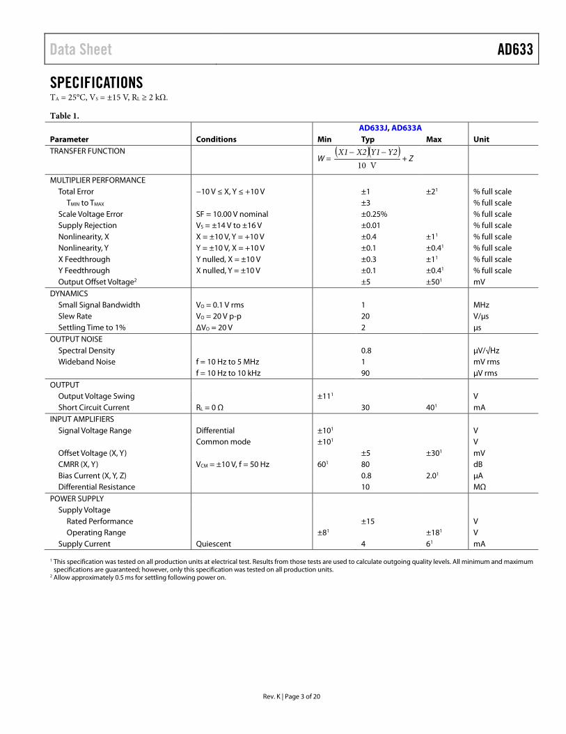
SPECIFICATIONS TA = 25°C, VS = ±15 V, RL ≥ 2 kΩ.
Table 1. AD633J, AD633A Parameter Conditions Min Typ Max Unit TRANSFER FUNCTION
W = ( )( )
V10Y2Y1X2X1 −−
+ Z
MULTIPLIER PERFORMANCE Total Error −10 V ≤ X, Y ≤ +10 V ±1 ±21 % full scale
TMIN to TMAX ±3 % full scale Scale Voltage Error SF = 10.00 V nominal ±0.25% % full scale Supply Rejection VS = ±14 V to ±16 V ±0.01 % full scale Nonlinearity, X X = ±10 V, Y = +10 V ±0.4 ±11 % full scale Nonlinearity, Y Y = ±10 V, X = +10 V ±0.1 ±0.41 % full scale X Feedthrough Y nulled, X = ±10 V ±0.3 ±11 % full scale Y Feedthrough X nulled, Y = ±10 V ±0.1 ±0.41 % full scale Output Offset Voltage2 ±5 ±501 mV
DYNAMICS Small Signal Bandwidth VO = 0.1 V rms 1 MHz Slew Rate VO = 20 V p-p 20 V/µs Settling Time to 1% ΔVO = 20 V 2 µs
OUTPUT NOISE Spectral Density 0.8 µV/√Hz Wideband Noise f = 10 Hz to 5 MHz 1 mV rms
f = 10 Hz to 10 kHz 90 µV rms OUTPUT
Output Voltage Swing ±111 V Short Circuit Current RL = 0 Ω 30 401 mA
INPUT AMPLIFIERS Signal Voltage Range Differential ±101 V Common mode ±101 V Offset Voltage (X, Y) ±5 ±301 mV CMRR (X, Y) VCM = ±10 V, f = 50 Hz 601 80 dB Bias Current (X, Y, Z) 0.8 2.01 µA Differential Resistance 10 MΩ
POWER SUPPLY Supply Voltage
Rated Performance ±15 V Operating Range ±81 ±181 V
Supply Current Quiescent 4 61 mA
1 This specification was tested on all production units at electrical test. Results from those tests are used to calculate outgoing quality levels. All minimum and maximum specifications are guaranteed; however, only this specification was tested on all production units.
2 Allow approximately 0.5 ms for settling following power on.
Rev. K | Page 3 of 20

AD633 Data Sheet
ABSOLUTE MAXIMUM RATINGS Table 2. Parameter Rating Supply Voltage ±18 V Internal Power Dissipation 500 mW Input Voltages1 ±18 V Output Short-Circuit Duration Indefinite Storage Temperature Range −65°C to +150°C Operating Temperature Range
AD633J 0°C to 70°C AD633A −40°C to +85°C
Lead Temperature (Soldering, 60 sec) 300°C ESD Rating 1000 V
1 For supply voltages less than ±18 V, the absolute maximum input voltage is equal to the supply voltage.
Stresses at or above those listed under Absolute Maximum Ratings may cause permanent damage to the product. This is a stress rating only; functional operation of the product at these or any other conditions above those indicated in the operational section of this specification is not implied. Operation beyond the maximum operating conditions for extended periods may affect product reliability.
THERMAL RESISTANCE θJA is specified for the worst-case conditions, that is, a device soldered in a circuit board for surface-mount packages.
Table 3. Package Type θJA Unit 8-Lead PDIP 90 °C/W 8-Lead SOIC 155 °C/W
ESD CAUTION
Rev. K | Page 4 of 20

Data Sheet AD633
Rev. K | Page 5 of 20
PIN CONFIGURATIONS AND FUNCTION DESCRIPTIONS
AD633JN/AD633AN
1
1
A
110V
1X1
2X2
3Y1
4Y2
8 +VS
7 W
Z6
5 –VS
0078
6-00
1
W = + Z(X1 – X2)(Y1 – Y2)
10V
Figure 2. 8-Lead PDIP
AD633JR/AD633AR
11
110V
1Y1
2Y2
3–VS
4Z
8 X2
7 X1
+VS6
5 W
0078
6-00
2
A
W = + Z(X1 – X2)(Y1 – Y2)
10V
Figure 3. 8-Lead SOIC
Table 4. 8-Lead PDIP Pin Function Descriptions Pin No. Mnemonic Description 1 X1 X Multiplicand Noninverting Input 2 X2 X Multiplicand Inverting Input 3 Y1 Y Multiplicand Noninverting Input 4 Y2 Y Multiplicand Inverting Input 5 −VS Negative Supply Rail 6 Z Summing Input 7 W Product Output 8 +VS Positive Supply Rail
Table 5. 8-Lead SOIC Pin Function Descriptions Pin No. Mnemonic Description 1 Y1 Y Multiplicand Noninverting Input 2 Y2 Y Multiplicand Inverting Input 3 −VS Negative Supply Rail 4 Z Summing Input 5 W Product Output 6 +VS Positive Supply Rail 7 X1 X Multiplicand Noninverting Input 8 X2 X Multiplicand Inverting Input
AD633 Data Sheet
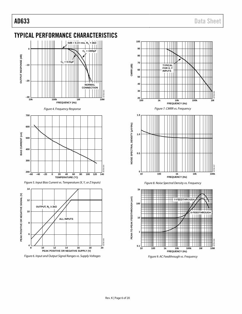
TYPICAL PERFORMANCE CHARACTERISTICS
FREQUENCY (Hz)
OU
TPU
T R
ESPO
NSE
(dB
)
0
–10
–20
–3010k 100k 1M 10M
0078
6-00
3
NORMALCONNECTION
0dB = 0.1V rms, RL = 2kΩ
CL = 1000pF
CL = 0.01µF
Figure 4. Frequency Response
TEMPERATURE (°C)
BIA
S C
UR
REN
T (n
A)
700
500
600
400
300
200–60 –40 –20 0 14012010080604020
0078
6-00
4
Figure 5. Input Bias Current vs. Temperature (X, Y, or Z Inputs)
PEAK POSITIVE OR NEGATIVE SUPPLY (V)
PEA
K P
OSI
TIVE
OR
NEG
ATIV
E SI
GN
AL (V
)
14
10
12
8
6
48 10 12 14 201816
0078
6-00
5
OUTPUT, RL ≥ 2kΩ
ALL INPUTS
Figure 6. Input and Output Signal Ranges vs. Supply Voltages
FREQUENCY (Hz)
CM
RR
(dB
)
100
60
50
90
80
70
40
30
20100 1k 1M100k10k
0078
6-00
6
TYPICALFOR X, YINPUTS
Figure 7. CMRR vs. Frequency
FREQUENCY (Hz)
NO
ISE
SPEC
TRA
L D
ENSI
T Y (µ
V/H
z)
1.5
1.0
0.5
010 100 1k 100k10k
0078
6-00
7
Figure 8. Noise Spectral Density vs. Frequency
FREQUENCY (Hz)
PEA
K-T
O-P
EAK
FEE
DTH
RO
UG
H (m
V)
1k
10
100
1
0.110 100 1k 10M10k 100k 1M
0078
6-00
8
Y-FEEDTHROUGH
X-FEEDTHROUGH
Figure 9. AC Feedthrough vs. Frequency
Rev. K | Page 6 of 20

Data Sheet AD633
TIME (Minutes)1.0 1.5
OU
TPU
T (±
mV)
2.52.0
−1
2
1
3.53.00.5
0
4.0 4.50
3
5.0
−2
−3
0078
6-00
9
Figure 10. Typical VOS vs. Time, For Five Minutes Following Power Up
Rev. K | Page 7 of 20

AD633 Data Sheet
FUNCTIONAL DESCRIPTION The AD633 is a low cost multiplier comprising a translinear core, a buried Zener reference, and a unity-gain connected output amplifier with an accessible summing node. Figure 1 shows the functional block diagram. The differential X and Y inputs are converted to differential currents by voltage-to-current converters. The product of these currents is generated by the multiplying core. A buried Zener reference provides an overall scale factor of 10 V. The sum of (X × Y)/10 + Z is then applied to the output amplifier. The amplifier summing Node Z allows the user to add two or more multiplier outputs, convert the output voltage to a current, and configure various analog computational functions.
Inspection of the block diagram shows the overall transfer function is
( )( )Z
Y2Y1X2X1W +
−−=
V10 (1)
ERROR SOURCES Multiplier errors consist primarily of input and output offsets, scale factor error, and nonlinearity in the multiplying core. The input and output offsets can be eliminated by using the optional trim of Figure 11. This scheme reduces the net error to scale factor errors (gain error) and an irreducible nonlinearity component in the multiplying core. The X and Y nonlinearities are typically 0.4% and 0.1% of full scale, respectively. Scale factor error is typically 0.25% of full scale. The high impedance Z input should always reference the ground point of the driven system, particularly if it is remote. Likewise, the differential X and Y inputs should reference their respective grounds to realize the full accuracy of the AD633.
±50mVTO APPROPRIATEINPUT TERMINAL(FOR EXAMPLE, X2, Y2, Z)
50kΩ1kΩ
300kΩ
+VS
–VS 0078
6-01
0
Figure 11. Optional Offset Trim Configuration
Rev. K | Page 8 of 20

Data Sheet AD633
APPLICATIONS INFORMATION The AD633 is well suited for such applications as modulation and demodulation, automatic gain control, power measurement, voltage-controlled amplifiers, and frequency doublers. These applications show the pin connections for the AD633JN (8-lead PDIP), which differs from the AD633JR (8-lead SOIC).
MULTIPLIER CONNECTIONS Figure 12 shows the basic connections for multiplication. The X and Y inputs normally have their negative nodes grounded, but they are fully differential, and in many applications, the grounded inputs may be reversed (to facilitate interfacing with signals of a particular polarity while achieving some desired output polarity), or both may be driven.
AD633JN
X11
X22
Y13
Y24
+VS 8
W 7
Z 6
–VS 5
XINPUT
YINPUT
+
–
+
–
0.1µF
0.1µF
+15V
–15V
OPTIONAL SUMMINGINPUT, Z
W = + Z(X1 – X2)(Y1 – Y2)10V
0078
6-01
1
Figure 12. Basic Multiplier Connections (See the Model Results Section)
SQUARING AND FREQUENCY DOUBLING As is shown in Figure 13, squaring of an input signal, E, is achieved simply by connecting the X and Y inputs in parallel to produce an output of E2/10 V. The input can have either polarity, but the output is positive. However, the output polarity can be reversed by interchanging the X or Y inputs. The Z input can be used to add a further signal to the output.
AD633JN
X11E
X22
Y13
Y24
+VS 8
W 7
Z 6
–VS 5
0.1µF
0.1µF
+15V
–15V
W = E2
10V
0078
6-01
2
Figure 13. Connections for Squaring
When the input is a sine wave E sin ωt, this squarer behaves as a frequency doubler, because
( ) ( )tEtEω−=
ω2cos1
V20V10sin 22
(2)
Equation 2 shows a dc term at the output that varies strongly with the amplitude of the input, E. This can be avoided using the connections shown in Figure 14, where an RC network is used to generate two signals whose product has no dc term. It uses the identity
( )θθθ 2sin21sincos = (3)
AD633JN
X11
X22
Y13
Y24
+VS 8
W 7
Z 6
–VS 5
0.1µF
0.1µF
+15V
–15V
W = E2
10V
0078
6-01
3
E
R
C R23kΩ
R11kΩ
Figure 14. Bounceless Frequency Doubler (See the Model Results Section)
At ωo = 1/CR, the X input leads the input signal by 45° (and is attenuated by √2), and the Y input lags the X input by 45° (and is also attenuated by √2). Because the X and Y inputs are 90° out of phase, the response of the circuit is (satisfying Equation 3)
( ) ( ) ( )°+ω°+ω= 45sin2
45sin2V10
100 tEtEW
( ) ( )tE0
2
2sinV40
ω= (4)
which has no dc component. Resistor R1 and Resistor R2 are included to restore the output amplitude to 10 V for an input amplitude of 10 V.
The amplitude of the output is only a weak function of frequency; the output amplitude is 0.5% too low at ω = 0.9 ω0 and ω0 = 1.1 ω0.
GENERATING INVERSE FUNCTIONS Inverse functions of multiplication, such as division and square rooting, can be implemented by placing a multiplier in the feedback loop of an op amp. Figure 15 shows how to implement square rooting with the transfer function for the condition E < 0.
The 1N4148 diode is required to prevent latchup, which can occur in such applications if the input were to change polarity, even momentarily.
( )V10EW −= (5)
AD633JN
X11
X22
Y13
Y24
+VS 8
W 7
Z 6
–VS 5
0.1µF
E < 0V
–15V
+15V
AD711
0.1µF
10kΩ
10kΩ
0007
86-0
14
0.1µF
W = √ –(10V)E
0.01µF
+15V
–15V
7
43
6
2
0.1µF
1N4148
Figure 15. Connections for Square Rooting
Rev. K | Page 9 of 20
AD633 Data Sheet
Rev. K | Page 10 of 20
Likewise, Figure 16 shows how to implement a divider using a multiplier in a feedback loop. The transfer function for the divider is
XE
EW V10 (6)
AD633JN
X11
X22
Y13
Y24
+VS 8
W 7
Z 6
–VS 5
0.1µF
0.1µF
+15V
0.1µF
+15V
0.1µF
–15V
–15V00
786-
015
7
43
6
2
AD711
E
R10kΩ
R10kΩ
EX
W' = –10VE
EX Figure 16. Connections for Division
VARIABLE SCALE FACTOR In some instances, it may be desirable to use a scaling voltage other than 10 V. The connections shown in Figure 17 increase the gain of the system by the ratio (R1 + R2)/R1. This ratio is limited to 100 in practical applications. The summing input, S, can be used to add an additional signal to the output, or it can be grounded.
AD633JN
X11
X22
Y13
Y24
+VS 8
W 7
Z 6
–VS 5
0.1µF
0.1µF
+15V
–15V
W =
0078
6-01
6
S
R1
R2
1kΩ ≤ R1, R2 ≤ 100kΩ
+ S(X1 – X2)(Y1 – Y2)
10V
R1 + R2
R1
XINPUT
YINPUT
+
–
+
–
Figure 17. Connections for Variable Scale Factor
CURRENT OUTPUT The voltage output of the AD633 can be converted to a current output by the addition of a resistor, R, between the W and Z pins of the AD633 as shown in Figure 18.
AD633JN
X11
X22
Y13
Y24
+VS 8
W 7
Z 6
–VS 5
0.1µF
0.1µF
+15V
–15V
IO =1
R
0078
6-01
7
(X1 – X2)(Y1 – Y2)
10V
1kΩ ≤ R ≤ 100kΩ
RX
INPUT
YINPUT
+
–
+
–
Figure 18. Current Output Connections
This arrangement forms the basis of voltage-controlled integrators and oscillators as is shown later in this section. The transfer function of this circuit has the form
V10
1 Y2Y1X2X1R
IO
(7)
LINEAR AMPLITUDE MODULATOR The AD633 can be used as a linear amplitude modulator with no external components. Figure 19 shows the circuit. The carrier and modulation inputs to the AD633 are multiplied to produce a double sideband signal. The carrier signal is fed forward to the Z input of the AD633 where it is summed with the double sideband signal to produce a double sideband with the carrier output.
AD633JN
X1MODULATIONINPUT
±EM
CARRIERINPUT
EC sin ωt
1
X22
Y13
Y24
+VS 8
W 7
Z 6
–VS 5
+
–
0.1µF
0.1µF
+15V
–15V
W = EC sin ωt
0078
6-01
8
EM
10V1+
Figure 19. Linear Amplitude Modulator
VOLTAGE-CONTROLLED, LOW-PASS AND HIGH-PASS FILTERS Figure 20 shows a single multiplier used to build a voltage-controlled, low-pass filter. The voltage at Output A is a result of filtering ES. The break frequency is modulated by EC, the control input. The break frequency, f2, equals
)2(10 RC
Ef C
2
(8)
and the roll-off is 6 dB per octave. This output, which is at a high impedance point, may need to be buffered.
AD633JN
X11
X22
Y13
Y24
+VS 8
W 7
Z 6
–VS 5
CONTROLINPUT EC
SIGNALINPUT ES
0.1µF
0.1µF
+15V
–15V
0078
6-01
9
R
C
1 + T1P
1 + T2POUTPUT B =
1
1 + T2POUTPUT A =
1
ω1T1 = = RC
1
ω2
10RC
ECT2 = =
dB
f2 f1f
–6dB/OCTAVEOUTPUT A
OUTPUT B
0
Figure 20. Voltage-Controlled, Low-Pass Filter
The voltage at Output B, the direct output of the AD633, has the same response up to frequency f1, the natural breakpoint of RC filter, and then levels off to a constant attenuation of f1/f2 = 10/EC
RCf
21
1 (9)
Data Sheet AD633
Rev. K | Page 11 of 20
For example, if R = 8 kΩ and C = 0.002 μF, then Output A has a pole at frequencies from 100 Hz to 10 kHz for EC ranging from 100 mV to 10 V. Output B has an additional 0 at 10 kHz (and can be loaded because it is the low impedance output of the multiplier). The circuit can be changed to a high-pass filter Z interchanging the resistor and capacitor as shown in Figure 21.
AD633JN
X11
X22
Y13
Y24
+VS 8
W 7
Z 6
–VS 5
CONTROLINPUT EC
SIGNALINPUT ES
0.1µF
0.1µF
+15V
–15V00
786-
020
R
C
OUTPUT B
OUTPUT A
dB
f1 f2f
+6dB/OCTAVEOUTPUT A
OUTPUT B
0
Figure 21. Voltage-Controlled, High-Pass Filter
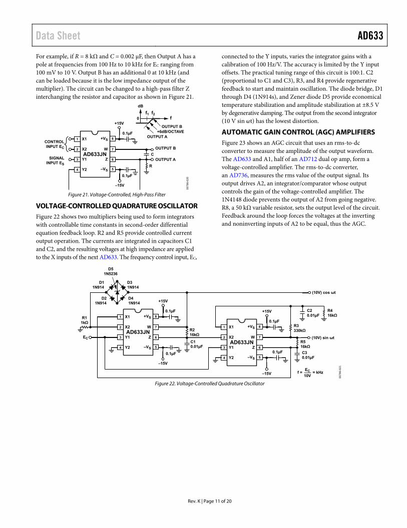
VOLTAGE-CONTROLLED QUADRATURE OSCILLATOR Figure 22 shows two multipliers being used to form integrators with controllable time constants in second-order differential equation feedback loop. R2 and R5 provide controlled current output operation. The currents are integrated in capacitors C1 and C2, and the resulting voltages at high impedance are applied to the X inputs of the next AD633. The frequency control input, EC,
connected to the Y inputs, varies the integrator gains with a calibration of 100 Hz/V. The accuracy is limited by the Y input offsets. The practical tuning range of this circuit is 100:1. C2 (proportional to C1 and C3), R3, and R4 provide regenerative feedback to start and maintain oscillation. The diode bridge, D1 through D4 (1N914s), and Zener diode D5 provide economical temperature stabilization and amplitude stabilization at ±8.5 V by degenerative damping. The output from the second integrator (10 V sin ωt) has the lowest distortion.
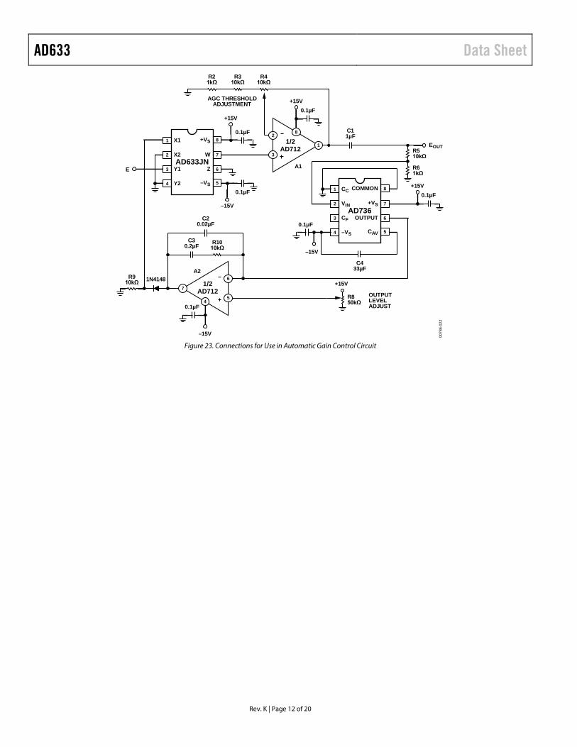
AUTOMATIC GAIN CONTROL (AGC) AMPLIFIERS Figure 23 shows an AGC circuit that uses an rms-to-dc converter to measure the amplitude of the output waveform. The AD633 and A1, half of an AD712 dual op amp, form a voltage-controlled amplifier. The rms-to-dc converter, an AD736, measures the rms value of the output signal. Its output drives A2, an integrator/comparator whose output controls the gain of the voltage-controlled amplifier. The 1N4148 diode prevents the output of A2 from going negative. R8, a 50 kΩ variable resistor, sets the output level of the circuit. Feedback around the loop forces the voltages at the inverting and noninverting inputs of A2 to be equal, thus the AGC.
AD633JN
X11
X22
Y13
Y24
+VS 8
W 7
Z 6
–VS 5
0.1µF
0.1µF
C10.01µF
+15V
–15V
AD633JN
X11
X22
Y13
Y24
+VS 8
W 7
Z 6
–VS 5
0.1µF
+15V
–15V
R516kΩ
R3330kΩ
R416kΩ
C30.01µF
C20.01µF
(10V) sin ωt
0.1µF
R216kΩ
R11kΩ
D51N5236
D11N914
D21N914
D31N914
D41N914
f =EC
10V= kHz
(10V) cos ωt
EC00
786-
021
Figure 22. Voltage-Controlled Quadrature Oscillator
AD633 Data Sheet
AD633JN
X11
X22
Y13
Y24
+VS 8
W 7
Z 6
–VS 5
0.1µF
0.1µF
+15V
–15V
A1
0.1µF
0.1µF
0.1µF
+15V
+15V
+15V
–15V
8
3
1
21/2
AD712
AGC THRESHOLDADJUSTMENT
R21kΩ
R310kΩ
R410kΩ
C30.2µF R10
10kΩ
R910kΩ
R850kΩ
1/2AD712
A2
0.1µF
–15V
45
7
6
C20.02µF
C433µF
C11µF
1N4148
AD736
CC1
VIN2
CF3
–VS4
+VS
8COMMON
OUTPUT
7
6
CAV 5
OUTPUTLEVELADJUST
R510kΩ
R61kΩ
EOUT
E
0078
6-02
2
Figure 23. Connections for Use in Automatic Gain Control Circuit
Rev. K | Page 12 of 20
Data Sheet AD633
Rev. K | Page 13 of 20
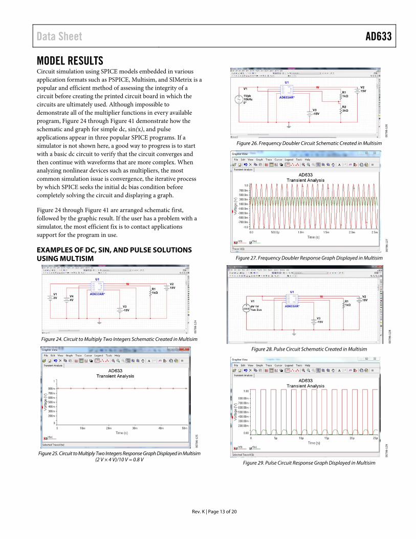
MODEL RESULTS Circuit simulation using SPICE models embedded in various application formats such as PSPICE, Multisim, and SIMetrix is a popular and efficient method of assessing the integrity of a circuit before creating the printed circuit board in which the circuits are ultimately used. Although impossible to demonstrate all of the multiplier functions in every available program, Figure 24 through Figure 41 demonstrate how the schematic and graph for simple dc, sin(x), and pulse applications appear in three popular SPICE programs. If a simulator is not shown here, a good way to progress is to start with a basic dc circuit to verify that the circuit converges and then continue with waveforms that are more complex. When analyzing nonlinear devices such as multipliers, the most common simulation issue is convergence, the iterative process by which SPICE seeks the initial dc bias condition before completely solving the circuit and displaying a graph.
Figure 24 through Figure 41 are arranged schematic first, followed by the graphic result. If the user has a problem with a simulator, the most efficient fix is to contact applications support for the program in use.
EXAMPLES OF DC, SIN, AND PULSE SOLUTIONS USING MULTISIM
0078
6-12
4
Figure 24. Circuit to Multiply Two Integers Schematic Created in Multisim
0078
6-12
5
Figure 25. Circuit to Multiply Two Integers Response Graph Displayed in Multisim
(2 V × 4 V)/10 V = 0.8 V
0078
6-12
6
Figure 26. Frequency Doubler Circuit Schematic Created in Multisim
0078
6-12
7
Figure 27. Frequency Doubler Response Graph Displayed in Multisim
0078
6-12
8
Figure 28. Pulse Circuit Schematic Created in Multisim
0078
6-12
9
Figure 29. Pulse Circuit Response Graph Displayed in Multisim
AD633 Data Sheet
Rev. K | Page 14 of 20
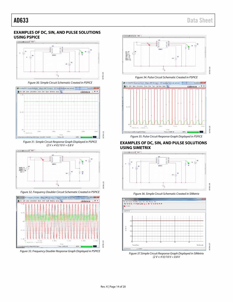
EXAMPLES OF DC, SIN, AND PULSE SOLUTIONS USING PSPICE
0078
6-13
0
Figure 30. Simple Circuit Schematic Created in PSPICE
0078
6-13
1
Figure 31. Simple Circuit Response Graph Displayed in PSPICE
(2 V × 4 V)/10 V = 0.8 V
0078
6-13
2
Figure 32. Frequency Doubler Circuit Schematic Created in PSPICE
0078
6-13
3
Figure 33. Frequency Doubler Response Graph Displayed in PSPICE
0078
6-13
4
Figure 34. Pulse Circuit Schematic Created in PSPICE
0078
6-13
5
Figure 35. Pulse Circuit Response Graph Displayed in PSPICE
EXAMPLES OF DC, SIN, AND PULSE SOLUTIONS USING SIMETRIX
0078
6-13
6
Figure 36. Simple Circuit Schematic Created in SIMetrix
0078
6-13
7
Figure 37.Simple Circuit Response Graph Displayed in SIMetrix
(2 V × 4 V)/10 V = 0.8 V
Data Sheet AD633
Rev. K | Page 15 of 20
0078
6-13
8
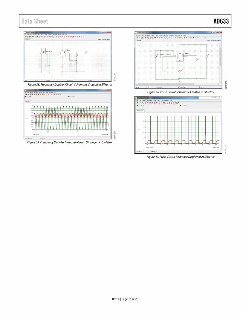
Figure 38. Frequency Doubler Circuit Schematic Created in SIMetrix
0078
6-13
9
Figure 39. Frequency Doubler Response Graph Displayed in SIMetrix
0078
6-14
0
Figure 40. Pulse Circuit Schematic Created in SIMetrix
0078
6-14
1
Figure 41. Pulse Circuit Response Displayed in SIMetrix
AD633 Data Sheet
Rev. K | Page 16 of 20
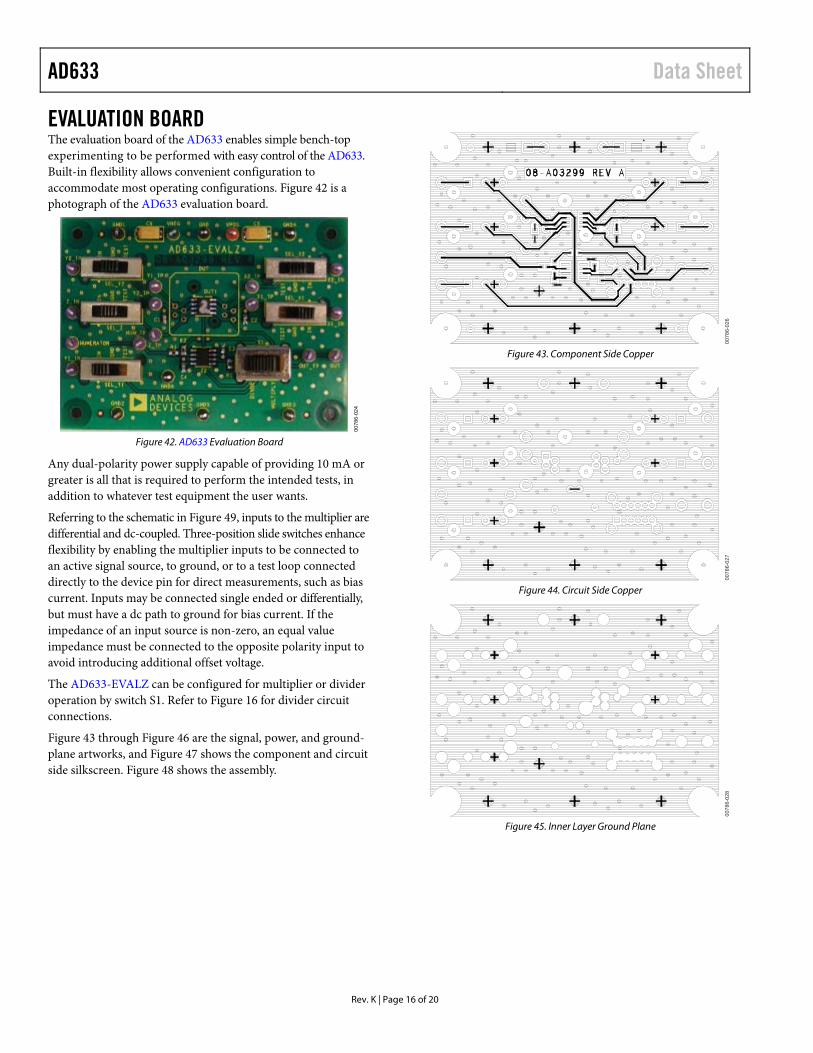
EVALUATION BOARD The evaluation board of the AD633 enables simple bench-top experimenting to be performed with easy control of the AD633. Built-in flexibility allows convenient configuration to accommodate most operating configurations. Figure 42 is a photograph of the AD633 evaluation board.
0078
6-02
4
Figure 42. AD633 Evaluation Board
Any dual-polarity power supply capable of providing 10 mA or greater is all that is required to perform the intended tests, in addition to whatever test equipment the user wants.
Referring to the schematic in Figure 49, inputs to the multiplier are differential and dc-coupled. Three-position slide switches enhance flexibility by enabling the multiplier inputs to be connected to an active signal source, to ground, or to a test loop connected directly to the device pin for direct measurements, such as bias current. Inputs may be connected single ended or differentially, but must have a dc path to ground for bias current. If the impedance of an input source is non-zero, an equal value impedance must be connected to the opposite polarity input to avoid introducing additional offset voltage.
The AD633-EVALZ can be configured for multiplier or divider operation by switch S1. Refer to Figure 16 for divider circuit connections.
Figure 43 through Figure 46 are the signal, power, and ground-plane artworks, and Figure 47 shows the component and circuit side silkscreen. Figure 48 shows the assembly.
0078
6-02
6
Figure 43. Component Side Copper
0078
6-02
7
Figure 44. Circuit Side Copper
0078
6-02
8
Figure 45. Inner Layer Ground Plane

Data Sheet AD633
Rev. K | Page 17 of 20
0078
6-02
9
Figure 46. Inner Layer Power Plane
0078
6-03
0
Figure 47. Component Side Silk Screen
0078
6-03
1
Figure 48. AD633-EVALZ Assembly
1 8
7
6
54
3
2
Y1
Y2
–VS
X2
+VS
X1
WZC10.1µF
C20.1µF
C30.1µF
DUT1AD633ARZ
FUNCT(1)
R210kΩ 2
73
4
6Z2AD711
+V
OUT
+
–
M
D
NUMERATOR
X2_IN
FUNCT(2) M
D
S1
M
D
SELX1
SEL_X2SEL_Y1
SEL_Y2
++
GND G6G5G4G3G2G1+V −V
+V
+V
−V
−V
MULTIPLY:[(X1-X2)(Y1-Y2)/10V] + Z
DIVIDE:−10V (NUM/DENOM)
IN
TEST
GND
Y1_TP
X1_TPY2_TP
X2_TP
NOM_TP
OUT_TP
FUNCTION SWITCH – S1
C510µF25V
C610µF25V
Y1_IN
Y2_IN
–VS
IN
TEST
GND
IN
TEST
GND
X2_IN
IN
TEST
GND
SEL_Y2
Y2_TPZ_IN
IN
TEST
GND
C40.1µF
X1_IN(DENOM)
R1100Ω
R310kΩ
0078
6-03
2
Figure 49. Schematic of the AD633 Evaluation Board

AD633 Data Sheet
Rev. K | Page 18 of 20
POWER SUPPLY
OUT – DMM
X INPUT DCVOLTAGE
Y INPUT DCVOLTAGE
0078
6-03
3
Figure 50. AD633-EVALZ Configured for Bench Experiments
Data Sheet AD633
Rev. K | Page 19 of 20
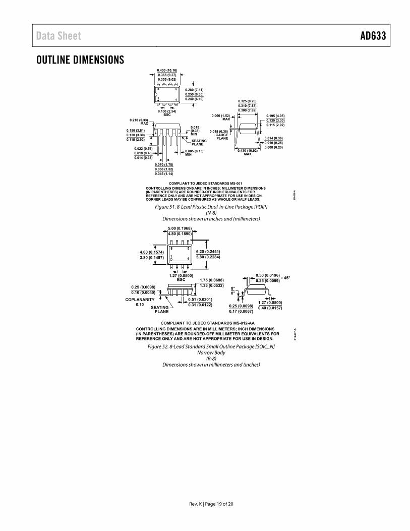
OUTLINE DIMENSIONS
COMPLIANT TO JEDEC STANDARDS MS-001
CONTROLLING DIMENSIONS ARE IN INCHES; MILLIMETER DIMENSIONS(IN PARENTHESES) ARE ROUNDED-OFF INCH EQUIVALENTS FORREFERENCE ONLY AND ARE NOT APPROPRIATE FOR USE IN DESIGN.CORNER LEADS MAY BE CONFIGURED AS WHOLE OR HALF LEADS. 0
706
06
-A
0.022 (0.56)0.018 (0.46)0.014 (0.36)
SEATINGPLANE
0.015(0.38)MIN
0.210 (5.33)MAX
0.150 (3.81)0.130 (3.30)0.115 (2.92)
0.070 (1.78)0.060 (1.52)0.045 (1.14)
8
1 4
5 0.280 (7.11)0.250 (6.35)0.240 (6.10)
0.100 (2.54)BSC
0.400 (10.16)0.365 (9.27)0.355 (9.02)
0.060 (1.52)MAX
0.430 (10.92)MAX
0.014 (0.36)0.010 (0.25)0.008 (0.20)
0.325 (8.26)0.310 (7.87)0.300 (7.62)
0.195 (4.95)0.130 (3.30)0.115 (2.92)
0.015 (0.38)GAUGEPLANE
0.005 (0.13)MIN
Figure 51. 8-Lead Plastic Dual-in-Line Package [PDIP]
(N-8) Dimensions shown in inches and (millimeters)
CONTROLLING DIMENSIONS ARE IN MILLIMETERS; INCH DIMENSIONS(IN PARENTHESES) ARE ROUNDED-OFF MILLIMETER EQUIVALENTS FORREFERENCE ONLY AND ARE NOT APPROPRIATE FOR USE IN DESIGN.
COMPLIANT TO JEDEC STANDARDS MS-012-AA
0124
07-A
0.25 (0.0098)0.17 (0.0067)
1.27 (0.0500)0.40 (0.0157)
0.50 (0.0196)0.25 (0.0099)
45°
8°0°
1.75 (0.0688)1.35 (0.0532)
SEATINGPLANE
0.25 (0.0098)0.10 (0.0040)
41
8 5
5.00 (0.1968)4.80 (0.1890)
4.00 (0.1574)3.80 (0.1497)
1.27 (0.0500)BSC
6.20 (0.2441)5.80 (0.2284)
0.51 (0.0201)0.31 (0.0122)
COPLANARITY0.10
Figure 52. 8-Lead Standard Small Outline Package [SOIC_N]
Narrow Body (R-8)
Dimensions shown in millimeters and (inches)
AD633 Data Sheet
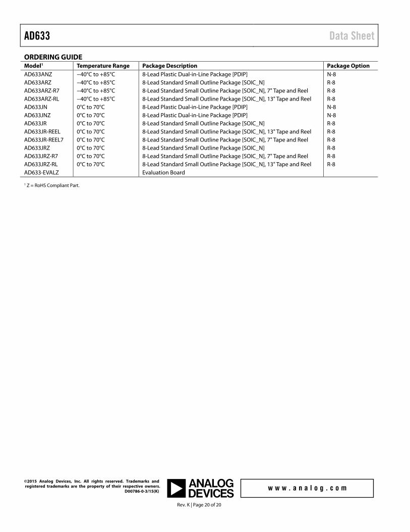
ORDERING GUIDE Model1 Temperature Range Package Description Package Option AD633ANZ −40°C to +85°C 8-Lead Plastic Dual-in-Line Package [PDIP] N-8 AD633ARZ −40°C to +85°C 8-Lead Standard Small Outline Package [SOIC_N] R-8 AD633ARZ-R7 −40°C to +85°C 8-Lead Standard Small Outline Package [SOIC_N], 7" Tape and Reel R-8 AD633ARZ-RL −40°C to +85°C 8-Lead Standard Small Outline Package [SOIC_N], 13" Tape and Reel R-8 AD633JN 0°C to 70°C 8-Lead Plastic Dual-in-Line Package [PDIP] N-8 AD633JNZ 0°C to 70°C 8-Lead Plastic Dual-in-Line Package [PDIP] N-8 AD633JR 0°C to 70°C 8-Lead Standard Small Outline Package [SOIC_N] R-8 AD633JR-REEL 0°C to 70°C 8-Lead Standard Small Outline Package [SOIC_N], 13" Tape and Reel R-8 AD633JR-REEL7 0°C to 70°C 8-Lead Standard Small Outline Package [SOIC_N], 7" Tape and Reel R-8 AD633JRZ 0°C to 70°C 8-Lead Standard Small Outline Package [SOIC_N] R-8 AD633JRZ-R7 0°C to 70°C 8-Lead Standard Small Outline Package [SOIC_N], 7" Tape and Reel R-8 AD633JRZ-RL 0°C to 70°C 8-Lead Standard Small Outline Package [SOIC_N], 13" Tape and Reel R-8 AD633-EVALZ Evaluation Board
1 Z = RoHS Compliant Part.
©2015 Analog Devices, Inc. All rights reserved. Trademarks and registered trademarks are the property of their respective owners. D00786-0-3/15(K)
Rev. K | Page 20 of 20