analysis of a three-phase flying converter cell rectifier
TRANSCRIPT
Analysis of a Three-Phase Flying Converter CellRectifier Operating in Light/No-Load Condition
M. Makoschitz∗, M. Hartmann† and H. Ertl∗∗ Institute of Energy Systems and Electrical Drives, Power Electronics Section
University of Technology Vienna, Austria; Email: [email protected]
† Schneider Electric Power Drives, Section Drives, Power ConversionVienna, Austria; Email: [email protected]
Abstract—The ”Flying” Converter Cell (FCC) rectifier allowsthe extension of an existing passive diode bridge rectifier to a low-harmonic unity power factor input stage by adding a combinationof additional converter topologies to the DC-side of the passivecircuit. In general, light-load condition of such an active rectifier,however, may lead to undesired effects as, e.g., impaired totalharmonic distortion of input currents (THDi). In this paper theoperation of the active rectifier circuit under no-load or light-loadconditions and corresponding effects are therefore analyzed in de-tail also considering the control of the two FCC DC voltages. Threedifferent operating modes are proposed and different parametersand characteristics of these modes are discussed accompanied bysimulation results. It is shown that the inductance value of thecoupled three-phase current injection choke directly influences theoperating behavior and design guidelines for this coupled inductorare therefore derived. This work further comprises a closer look atcurrent control and voltage balancing of FCC DC voltages duringlight- and no-load condition and resulting optimization issuesevoked due to appropriate control of dedicate control structures.Discussed side effects are finally verified by experimental resultstaken from a laboratory prototype of 10 kW output power and10 kHz switching frequency.
Index Terms—Three-Phase AC-DC Conversion, Third-Harmonic Injection, No-Load Operation
I. INTRODUCTIONActive three-phase PFC rectifier systems are widely used in
industry if high (unity) power factor and low harmonic inputcurrents are required. Topologies as, e.g., the six-switch boost-type PFC rectifier (bidirectional power flow) [1], [2], ViennaRectifier (unidirectional power flow) [3], six-switch buck-typePFC rectifier (unidirectional power flow, for positive dc outputvoltage), SWISS Rectifier (unidirectional power flow) [4] or the”hybrid third harmonic current injection active-filter rectifier”(unidirectional power flow) [1], [5] are perfectly suitable to full-fill the IEEE519/IEC61000-3-2 standards [6], [7] for mitigationof input current harmonics. Major drawbacks of these rectifierciruits are that (at least) two active semiconductor componentshave to process the full amount of output power and none ofthese structures can be used to extend an existing passive three-phase rectifier to a low harmonic input stage.
A hybrid system ([8]) based on the third harmonic injectionprinciple has therefore been introduced ([9]) which allowsthe extension of an existing passive three-phase diode bridgerectifier to a low-harmonic current input stage by adding anadditional converter stage - known as ”Flying” Converter Cell(FCC) active rectifier (see Fig. 1) - to the DC-side of the passivecircuit. The active system only needs to process some small
Fig. 1: Simplified schematic of an active rectifier circuit employing a ”Flying”converter cell as proposed in [9].
amount of the rated output power and therefore shows improvedefficiency, unity power factor (λ > 0.99) and low harmonicinput currents (THDi < 5%) (cf., [10]). The FCC basicallyconsists of three different converter topologies (two half-bridgesand one unidirectional three-level bridge leg). Both half-bridgeshave to inject such amount of current icp and icn into thepositive and negative busbar (primarily formed by the outputof the passive diode bridge rectifier) to guarantee sinusoidalwaveshapes ipos and ineg. The unidirectional three-level bridgeleg is cyclically connected to the AC-side mains and injects athird harmonic current ih3. The system only allows uncontrolledDC output voltage Vo which is defined by the mains voltagesVo = 3
√3VN
π during continuous conduction mode operation andno common-mode voltage components vCM with switchingfrequency fs appear.
Passive three-phase diode bridge rectifier circuits on the otherhand are a favourable solution for low-cost applications whichrequire high efficiency (ηB6 ≈ 99%) and increased input currentdistortion and reduced power factor are admissible. Due to thelow circuit complexity of the system side effects during lightand no-load mode (as for example increased output voltage) canbe easily adressed and investigated. The described modes arevery well known in literature, namely ”continuous conductionmode” (CCM) and ”discontinuous conduction mode” (DCM).DCM, however, has to be seperated into two different modes -DCMI and DCMII ([11]). The term CCM is typically referringto the state of the rectifiers inductor current iL. Consideringthe passive three-phase rectifier, CCM is applicable if the DC-
978-1-4799-6735-3/15/$31.00 ©2015 IEEE 92
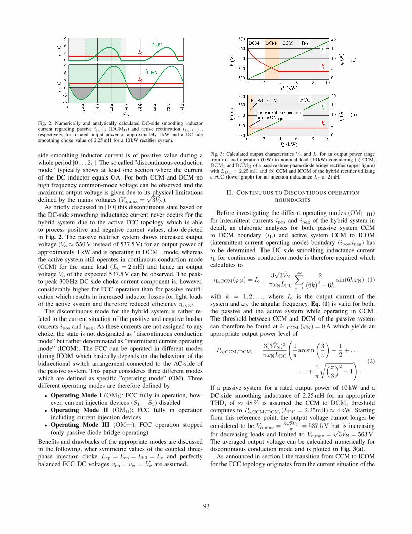
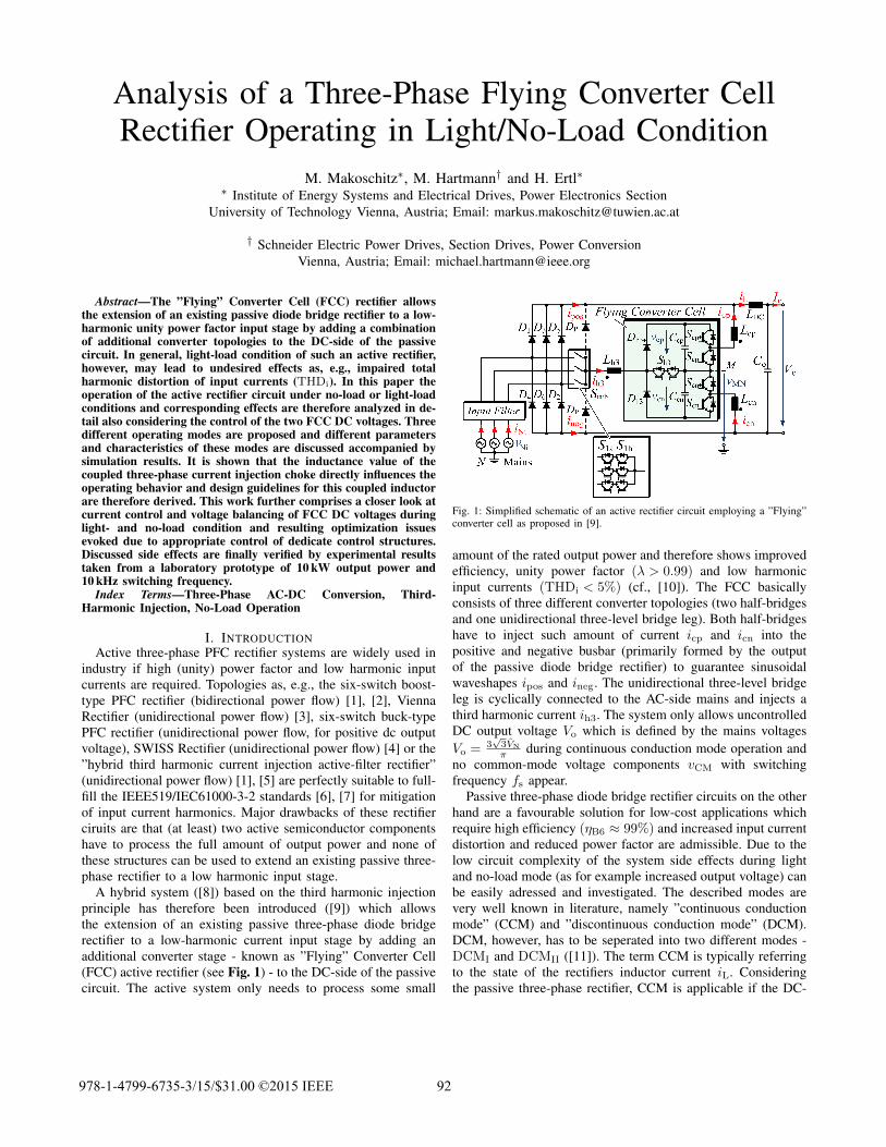
Fig. 2: Numerically and analytically calculated DC-side smoothing inductorcurrent regarding passive iL,B6 (DCMII) and active rectification iL,FCC ,respectively, for a rated output power of approximately 1 kW and a DC-sidesmoothing choke value of 2.25 mH for a 10 kW rectifier system.
side smoothing inductor current is of positive value during awhole period [0 . . . 2π]. The so called ”discontinuous conductionmode” typically shows at least one section where the currentof the DC inductor equals 0 A. For both CCM and DCM nohigh frequency common-mode voltage can be observed and themaximum output voltage is given due to its physical limitationsdefined by the mains voltages (Vo,max =
√3VN).
As briefly discussed in [10] this discontinuous state based onthe DC-side smoothing inductance current never occurs for thehybrid system due to the active FCC topology which is ableto process positive and negative current values, also depictedin Fig. 2. The passive rectifier system shows increased outputvoltage (Vo ≈ 550 V instead of 537.5 V) for an output power ofapproximately 1 kW and is operating in DCMII mode, whereasthe active system still operates in continuous conduction mode(CCM) for the same load (Lc = 2 mH) and hence an outputvoltage Vo of the expected 537.5 V can be observed. The peak-to-peak 300 Hz DC-side choke current component is, however,considerably higher for FCC operation than for passive rectifi-cation which results in increased inductor losses for light loadsof the active system and therefore reduced efficiency ηFCC.
The discontinuous mode for the hybrid system is rather re-lated to the current situation of the positive and negative busbarcurrents ipos and ineg. As these currents are not assigned to anychoke, the state is not designated as ”discontinuous conductionmode” but rather denominated as ”intermittent current operatingmode” (ICOM). The FCC can be operated in different modesduring ICOM which basically depends on the behaviour of thebidirectional switch arrangement connected to the AC-side ofthe passive system. This paper consideres three different modeswhich are defined as specific ”operating mode” (OM). Threedifferent operating modes are therefore defined by• Operating Mode I (OMI): FCC fully in operation, how-
ever, current injection devices (S1 − S3) disabled• Operating Mode II (OMII): FCC fully in operation
including current injection devices• Operating Mode III (OMIII): FCC operation stopped
(only passive diode bridge operating)Benefits and drawbacks of the appropriate modes are discussedin the following, wher symmetric values of the coupled three-phase injection choke Lcp = Lcn = Lh3 = Lc and perfectlybalanced FCC DC voltages vcp = vcn = Vc are assumed.
Fig. 3: Calculated output characteristics Vo and Io for an output power rangefrom no-load operation (0 W) to nominal load (10 kW) considering (a) CCM,DCMI and DCMII of a passive three-phase diode bridge rectifier (upper figure)with LDC = 2.25mH and (b) CCM and ICOM of the hybrid rectifier utilizinga FCC (lower graph) for an injection inductance Lc of 2 mH.
II. CONTINUOUS TO DISCONTIUOUS OPERATIONBOUNDARIES
Before investigating the differnt operating modes (OMI−III)for intermittent currents ipos and ineg of the hybrid system indetail, an elaborate analyzes for both, passive system CCMto DCM boundary (iL) and active system CCM to ICOM(intermittent current operating mode) boundary (ipos,ineg) hasto be determined. The DC-side smoothing inductance currentiL for continuous conduction mode is therefore required whichcalculates to
iL,CCM(ϕN) = Io −3√
3VN
πωNLDC
∞∑k=1
2
(6k)3 − 6k
sin(6kϕN) (1)
with k = 1, 2, . . ., where Io is the output current of thesystem and ωN the angular frequency. Eq. (1) is valid for both,the passive and the active system while operating in CCM.The threshold between CCM and DCM of the passive systemcan therefore be found at iL,CCM (ϕN) = 0 A which yields anappropriate output power level of
Po,CCM/DCMI=
3(3VN)2
πωNLDC
(1
πarcsin
(3
π
)− 1
2+ . . .
. . .+1
π
√(π3
)2
− 1
).
(2)
If a passive system for a rated output power of 10 kW and aDC-side smoothing inductance of 2.25 mH for an appropriateTHDi of ≈ 48 % is assumed the CCM to DCMI thresholdcomputes to Po,CCM/DCMI
(LDC = 2.25mH) ≈ 4 kW. Startingfrom this reference point, the output voltage cannot longer beconsidered to be Vo,max = 3
√3VN
π = 537.5 V but is increasingfor decreasing loads and limited to Vo,max =
√3VN = 563 V.
The averaged output voltage can be calculated numerically fordiscontinuous conduction mode and is plotted in Fig. 3(a).
As announced in section I the transition from CCM to ICOMfor the FCC topology originates from the current situation of the
93
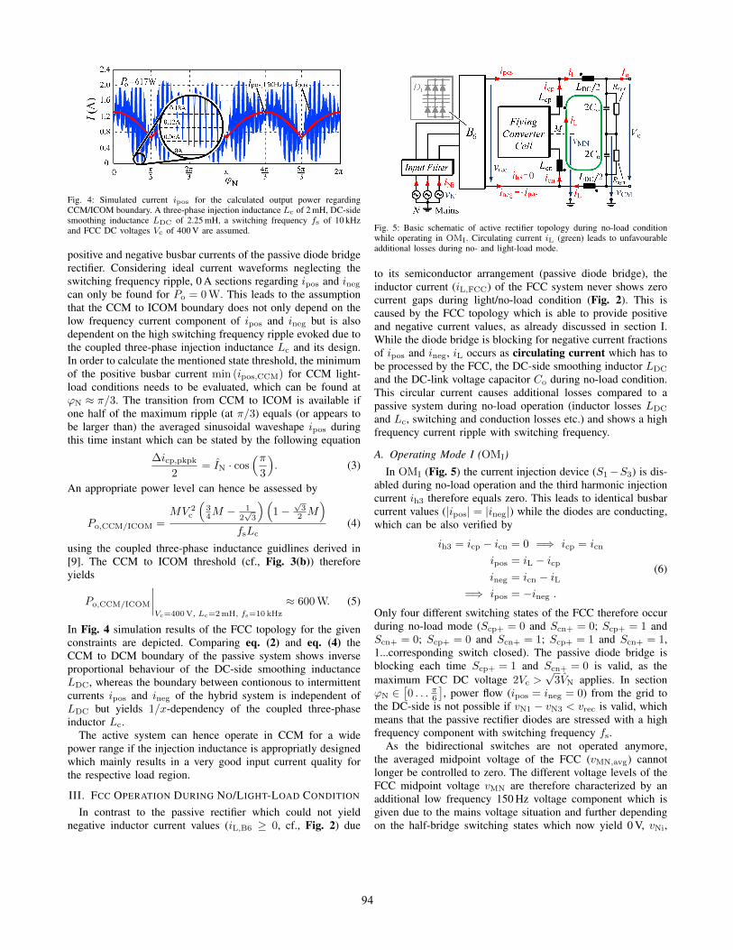
Fig. 4: Simulated current ipos for the calculated output power regardingCCM/ICOM boundary. A three-phase injection inductance Lc of 2 mH, DC-sidesmoothing inductance LDC of 2.25 mH, a switching frequency fs of 10 kHzand FCC DC voltages Vc of 400 V are assumed.
positive and negative busbar currents of the passive diode bridgerectifier. Considering ideal current waveforms neglecting theswitching frequency ripple, 0 A sections regarding ipos and ineg
can only be found for Po = 0 W. This leads to the assumptionthat the CCM to ICOM boundary does not only depend on thelow frequency current component of ipos and ineg but is alsodependent on the high switching frequency ripple evoked due tothe coupled three-phase injection inductance Lc and its design.In order to calculate the mentioned state threshold, the minimumof the positive busbar current min (ipos,CCM) for CCM light-load conditions needs to be evaluated, which can be found atϕN ≈ π/3. The transition from CCM to ICOM is available ifone half of the maximum ripple (at π/3) equals (or appears tobe larger than) the averaged sinusoidal waveshape ipos duringthis time instant which can be stated by the following equation
∆icp,pkpk
2= IN · cos
(π3
). (3)
An appropriate power level can hence be assessed by
Po,CCM/ICOM =MV 2
c
(34M −
12√
3
)(1−
√3
2 M)
fsLc(4)
using the coupled three-phase inductance guidlines derived in[9]. The CCM to ICOM threshold (cf., Fig. 3(b)) thereforeyields
Po,CCM/ICOM
∣∣∣∣Vc=400 V, Lc=2 mH, fs=10 kHz
≈ 600 W. (5)
In Fig. 4 simulation results of the FCC topology for the givenconstraints are depicted. Comparing eq. (2) and eq. (4) theCCM to DCM boundary of the passive system shows inverseproportional behaviour of the DC-side smoothing inductanceLDC, whereas the boundary between contionous to intermittentcurrents ipos and ineg of the hybrid system is independent ofLDC but yields 1/x-dependency of the coupled three-phaseinductor Lc.
The active system can hence operate in CCM for a widepower range if the injection inductance is appropriatly designedwhich mainly results in a very good input current quality forthe respective load region.
III. FCC OPERATION DURING NO/LIGHT-LOAD CONDITION
In contrast to the passive rectifier which could not yieldnegative inductor current values (iL,B6 ≥ 0, cf., Fig. 2) due
Fig. 5: Basic schematic of active rectifier topology during no-load conditionwhile operating in OMI. Circulating current iL (green) leads to unfavourableadditional losses during no- and light-load mode.
to its semiconductor arrangement (passive diode bridge), theinductor current (iL,FCC) of the FCC system never shows zerocurrent gaps during light/no-load condition (Fig. 2). This iscaused by the FCC topology which is able to provide positiveand negative current values, as already discussed in section I.While the diode bridge is blocking for negative current fractionsof ipos and ineg, iL occurs as circulating current which has tobe processed by the FCC, the DC-side smoothing inductor LDC
and the DC-link voltage capacitor Co during no-load condition.This circular current causes additional losses compared to apassive system during no-load operation (inductor losses LDC
and Lc, switching and conduction losses etc.) and shows a highfrequency current ripple with switching frequency.
A. Operating Mode I (OMI)
In OMI (Fig. 5) the current injection device (S1−S3) is dis-abled during no-load operation and the third harmonic injectioncurrent ih3 therefore equals zero. This leads to identical busbarcurrent values (|ipos| = |ineg|) while the diodes are conducting,which can be also verified by
ih3 = icp − icn = 0 =⇒ icp = icn
ipos = iL − icp
ineg = icn − iL=⇒ ipos = −ineg .
(6)
Only four different switching states of the FCC therefore occurduring no-load mode (Scp+ = 0 and Scn+ = 0; Scp+ = 1 andScn+ = 0; Scp+ = 0 and Scn+ = 1; Scp+ = 1 and Scn+ = 1,1...corresponding switch closed). The passive diode bridge isblocking each time Scp+ = 1 and Scn+ = 0 is valid, as themaximum FCC DC voltage 2Vc >
√3VN applies. In section
ϕN ∈[0 . . . π6
], power flow (ipos = ineg = 0) from the grid to
the DC-side is not possible if vN1 − vN3 < vrec is valid, whichmeans that the passive rectifier diodes are stressed with a highfrequency component with switching frequency fs.
As the bidirectional switches are not operated anymore,the averaged midpoint voltage of the FCC (vMN,avg) cannotlonger be controlled to zero. The different voltage levels of theFCC midpoint voltage vMN are therefore characterized by anadditional low frequency 150 Hz voltage component which isgiven due to the mains voltage situation and further dependingon the half-bridge switching states which now yield 0 V, vNi,
94
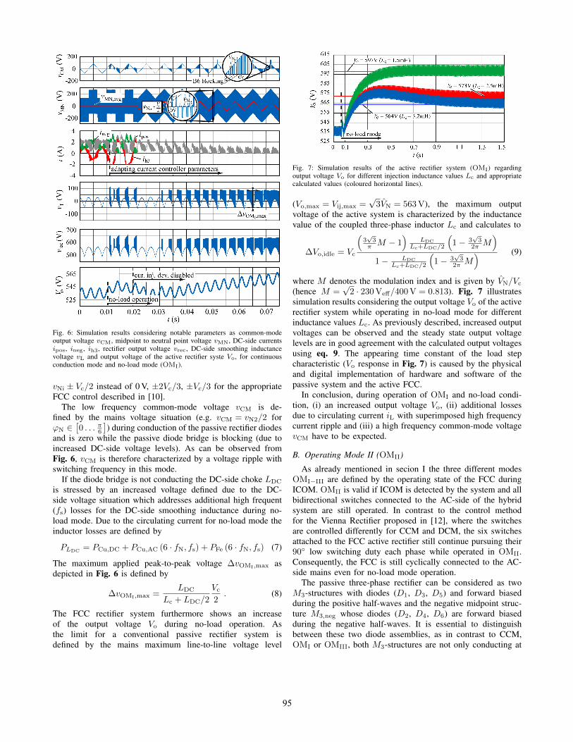
Fig. 6: Simulation results considering notable parameters as common-modeoutput voltage vCM, midpoint to neutral point voltage vMN, DC-side currentsipos, ineg, ih3, rectifier output voltage vrec, DC-side smoothing inductancevoltage vL and output voltage of the active rectifier syste Vo, for continuousconduction mode and no-load mode (OMI).
vNi ± Vc/2 instead of 0 V, ±2Vc/3, ±Vc/3 for the appropriateFCC control described in [10].
The low frequency common-mode voltage vCM is de-fined by the mains voltage situation (e.g. vCM = vN2/2 forϕN ∈
[0 . . . π6
]) during conduction of the passive rectifier diodes
and is zero while the passive diode bridge is blocking (due toincreased DC-side voltage levels). As can be observed fromFig. 6, vCM is therefore characterized by a voltage ripple withswitching frequency in this mode.
If the diode bridge is not conducting the DC-side choke LDC
is stressed by an increased voltage defined due to the DC-side voltage situation which addresses additional high frequent(fs) losses for the DC-side smoothing inductance during no-load mode. Due to the circulating current for no-load mode theinductor losses are defined by
PLDC= PCu,DC + PCu,AC (6 · fN, fs) + PFe (6 · fN, fs) (7)
The maximum applied peak-to-peak voltage ∆vOMI,max asdepicted in Fig. 6 is defined by
∆vOMI,max =LDC
Lc + LDC/2
Vc
2. (8)
The FCC rectifier system furthermore shows an increaseof the output voltage Vo during no-load operation. Asthe limit for a conventional passive rectifier system isdefined by the mains maximum line-to-line voltage level
Fig. 7: Simulation results of the active rectifier system (OMI) regardingoutput voltage Vo for different injection inductance values Lc and appropriatecalculated values (coloured horizontal lines).
(Vo,max = Vij,max =√
3VN = 563 V), the maximum outputvoltage of the active system is characterized by the inductancevalue of the coupled three-phase inductor Lc and calculates to
∆Vo,idle = Vc
(3√
3π M − 1
)LDC
Lc+LDC/2
(1− 3
√3
2π M)
1− LDC
Lc+LDC/2
(1− 3
√3
2π M) (9)
where M denotes the modulation index and is given by VN/Vc
(hence M =√
2 · 230 Veff/400 V = 0.813). Fig. 7 illustratessimulation results considering the output voltage Vo of the activerectifier system while operating in no-load mode for differentinductance values Lc. As previously described, increased outputvoltages can be observed and the steady state output voltagelevels are in good agreement with the calculated output voltagesusing eq. 9. The appearing time constant of the load stepcharacteristic (Vo response in Fig. 7) is caused by the physicaland digital implementation of hardware and software of thepassive system and the active FCC.
In conclusion, during operation of OMI and no-load condi-tion, (i) an increased output voltage Vo, (ii) additional lossesdue to circulating current iL with superimposed high frequencycurrent ripple and (iii) a high frequency common-mode voltagevCM have to be expected.
B. Operating Mode II (OMII)
As already mentioned in secion I the three different modesOMI−III are defined by the operating state of the FCC duringICOM. OMII is valid if ICOM is detected by the system and allbidirectional switches connected to the AC-side of the hybridsystem are still operated. In contrast to the control methodfor the Vienna Rectifier proposed in [12], where the switchesare controlled differently for CCM and DCM, the six switchesattached to the FCC active rectifier still continue pursuing their90◦ low switching duty each phase while operated in OMII.Consequently, the FCC is still cyclically connected to the AC-side mains even for no-load mode operation.
The passive three-phase rectifier can be considered as twoM3-structures with diodes (D1, D3, D5) and forward biasedduring the positive half-waves and the negative midpoint struc-ture M3,neg whose diodes (D2, D4, D6) are forward biasedduring the negative half-waves. It is essential to distinguishbetween these two diode assemblies, as in contrast to CCM,OMI or OMIII, both M3-structures are not only conducting at
95
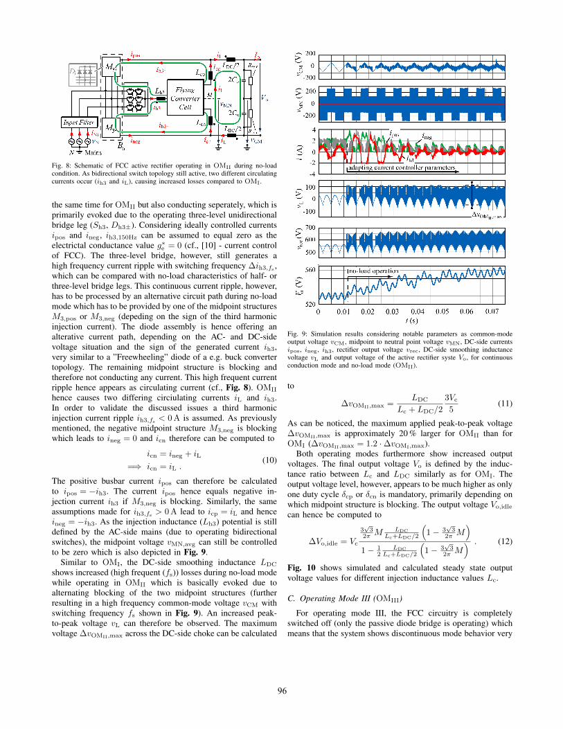
Fig. 8: Schematic of FCC active rectifier operating in OMII during no-loadcondition. As bidirectional switch topology still active, two different circulatingcurrents occur (ih3 and iL), causing increased losses compared to OMI.
the same time for OMII but also conducting seperately, which isprimarily evoked due to the operating three-level unidirectionalbridge leg (Sh3, Dh3±). Considering ideally controlled currentsipos and ineg, ih3,150Hz can be assumed to equal zero as theelectrictal conductance value g∗e = 0 (cf., [10] - current controlof FCC). The three-level bridge, however, still generates ahigh frequency current ripple with switching frequency ∆ih3,fs ,which can be compared with no-load characteristics of half- orthree-level bridge legs. This continuous current ripple, however,has to be processed by an alternative circuit path during no-loadmode which has to be provided by one of the midpoint structuresM3,pos or M3,neg (depeding on the sign of the third harmonicinjection current). The diode assembly is hence offering analterative current path, depending on the AC- and DC-sidevoltage situation and the sign of the generated current ih3,very similar to a ”Freewheeling” diode of a e.g. buck convertertopology. The remaining midpoint structure is blocking andtherefore not conducting any current. This high frequent currentripple hence appears as circulating current (cf., Fig. 8). OMII
hence causes two differing circiulating currents iL and ih3.In order to validate the discussed issues a third harmonicinjection current ripple ih3,fs < 0 A is assumed. As previouslymentioned, the negative midpoint structure M3,neg is blockingwhich leads to ineg = 0 and icn therefore can be computed to
icn = ineg + iL
=⇒ icn = iL .(10)
The positive busbar current ipos can therefore be calculatedto ipos = −ih3. The current ipos hence equals negative in-jection current ih3 if M3,neg is blocking. Similarly, the sameassumptions made for ih3,fs > 0 A lead to icp = iL and henceineg = −ih3. As the injection inductance (Lh3) potential is stilldefined by the AC-side mains (due to operating bidirectionalswitches), the midpoint voltage vMN,avg can still be controlledto be zero which is also depicted in Fig. 9.
Similar to OMI, the DC-side smoothing inductance LDC
shows increased (high frequent (fs)) losses during no-load modewhile operating in OMII which is basically evoked due toalternating blocking of the two midpoint structures (furtherresulting in a high frequency common-mode voltage vCM withswitching frequency fs shown in Fig. 9). An increased peak-to-peak voltage vL can therefore be observed. The maximumvoltage ∆vOMII,max across the DC-side choke can be calculated
Fig. 9: Simulation results considering notable parameters as common-modeoutput voltage vCM, midpoint to neutral point voltage vMN, DC-side currentsipos, ineg, ih3, rectifier output voltage vrec, DC-side smoothing inductancevoltage vL and output voltage of the active rectifier syste Vo, for continuousconduction mode and no-load mode (OMII).
to
∆vOMII,max =LDC
Lc + LDC/2
3Vc
5(11)
As can be noticed, the maximum applied peak-to-peak voltage∆vOMII,max is approximately 20 % larger for OMII than forOMI (∆vOMII,max = 1.2 ·∆vOMI,max).
Both operating modes furthermore show increased outputvoltages. The final output voltage Vo is defined by the induc-tance ratio between Lc and LDC similarly as for OMI. Theoutput voltage level, however, appears to be much higher as onlyone duty cycle δcp or δcn is mandatory, primarily depending onwhich midpoint structure is blocking. The output voltage Vo,idle
can hence be computed to
∆Vo,idle = Vc
3√
32π M
LDC
Lc+LDC/2
(1− 3
√3
2π M)
1− 12
LDC
Lc+LDC/2
(1− 3
√3
2π M) . (12)
Fig. 10 shows simulated and calculated steady state outputvoltage values for different injection inductance values Lc.
C. Operating Mode III (OMIII)
For operating mode III, the FCC circuitry is completelyswitched off (only the passive diode bridge is operating) whichmeans that the system shows discontinuous mode behavior very
96
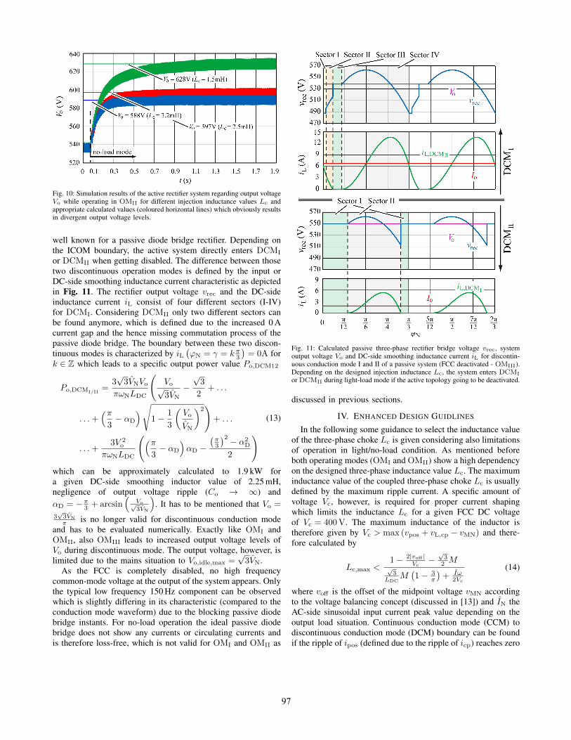
Fig. 10: Simulation results of the active rectifier system regarding output voltageVo while operating in OMII for different injection inductance values Lc andappropriate calculated values (coloured horizontal lines) which obviously resultsin divergent output voltage levels.
well known for a passive diode bridge rectifier. Depending onthe ICOM boundary, the active system directly enters DCMI
or DCMII when getting disabled. The difference between thosetwo discontinuous operation modes is defined by the input orDC-side smoothing inductance current characteristic as depictedin Fig. 11. The rectifier output voltage vrec and the DC-sideinductance current iL consist of four different sectors (I-IV)for DCMI. Considering DCMII only two different sectors canbe found anymore, which is defined due to the increased 0 Acurrent gap and the hence missing commutation process of thepassive diode bridge. The boundary between these two discon-tinuous modes is characterized by iL
(ϕN = γ = k π3
)= 0A for
k ∈ Z which leads to a specific output power value Po,DCM12
Po,DCMI/II=
3√
3VNVo
πωNLDC
(Vo√3VN
−√
3
2+ . . .
. . .+(π
3− αD
)√1− 1
3
(Vo
VN
)2)
+ . . .
. . .+3V 2
o
πωNLDC
((π3− αD
)αD −
(π3
)2 − α2D
2
) (13)
which can be approximately calculated to 1.9 kW fora given DC-side smoothing inductor value of 2.25 mH,negligence of output voltage ripple (Co → ∞) andαD = −π3 + arcsin
(Vo√3VN
). It has to be mentioned that Vo =
3√
3VN
π is no longer valid for discontinuous conduction modeand has to be evaluated numerically. Exactly like OMI andOMII, also OMIII leads to increased output voltage levels ofVo during discontinuous mode. The output voltage, however, islimited due to the mains situation to Vo,idle,max =
√3VN.
As the FCC is completely disabled, no high frequencycommon-mode voltage at the output of the system appears. Onlythe typical low frequency 150 Hz component can be observedwhich is slightly differing in its characteristic (compared to theconduction mode waveform) due to the blocking passive diodebridge instants. For no-load operation the ideal passive diodebridge does not show any currents or circulating currents andis therefore loss-free, which is not valid for OMI and OMII as
Fig. 11: Calculated passive three-phase rectifier bridge voltage vrec, systemoutput voltage Vo and DC-side smoothing inductance current iL for discontin-uous conduction mode I and II of a passive system (FCC deactivated - OMIII).Depending on the designed injection inductance Lc, the system enters DCMI
or DCMII during light-load mode if the active topology going to be deactivated.
discussed in previous sections.
IV. ENHANCED DESIGN GUIDLINES
In the following some guidance to select the inductance valueof the three-phase choke Lc is given considering also limitationsof operation in light/no-load condition. As mentioned beforeboth operating modes (OMI and OMII) show a high dependencyon the designed three-phase inductance value Lc. The maximuminductance value of the coupled three-phase choke Lc is usuallydefined by the maximum ripple current. A specific amount ofvoltage Vc, however, is required for proper current shapingwhich limits the inductance Lc for a given FCC DC voltageof Vc = 400 V. The maximum inductance of the inductor istherefore given by Vc > max (vpos + vL,cp − vMN) and there-fore calculated by
Lc,max <1− 2|voff |
Vc−√
32 M√
3LDC
M(1− 3
π
)+ Iω
2Vc
(14)
where voff is the offset of the midpoint voltage vMN accordingto the voltage balancing concept (discussed in [13]) and IN theAC-side sinusoidal input current peak value depending on theoutput load situation. Continuous conduction mode (CCM) todiscontinuous conduction mode (DCM) boundary can be foundif the ripple of ipos (defined due to the ripple of icp) reaches zero
97
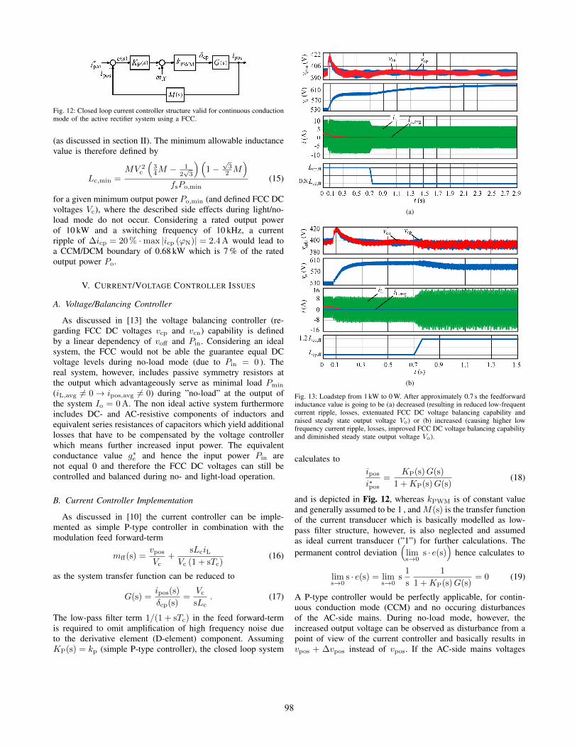
Fig. 12: Closed loop current controller structure valid for continuous conductionmode of the active rectifier system using a FCC.
(as discussed in section II). The minimum allowable inductancevalue is therefore defined by
Lc,min =MV 2
c
(34M −
12√
3
)(1−
√3
2 M)
fsPo,min(15)
for a given minimum output power Po,min (and defined FCC DCvoltages Vc), where the described side effects during light/no-load mode do not occur. Considering a rated output powerof 10 kW and a switching frequency of 10 kHz, a currentripple of ∆icp = 20 % ·max |icp (ϕN)| = 2.4 A would lead toa CCM/DCM boundary of 0.68 kW which is 7 % of the ratedoutput power Po.
V. CURRENT/VOLTAGE CONTROLLER ISSUES
A. Voltage/Balancing Controller
As discussed in [13] the voltage balancing controller (re-garding FCC DC voltages vcp and vcn) capability is definedby a linear dependency of voff and Pin. Considering an idealsystem, the FCC would not be able the guarantee equal DCvoltage levels during no-load mode (due to Pin = 0 ). Thereal system, however, includes passive symmetry resistors atthe output which advantageously serve as minimal load Pmin
(iL,avg 6= 0→ ipos,avg 6= 0) during ”no-load” at the output ofthe system Io = 0 A. The non ideal active system furthermoreincludes DC- and AC-resistive components of inductors andequivalent series resistances of capacitors which yield additionallosses that have to be compensated by the voltage controllerwhich means further increased input power. The equivalentconductance value g∗e and hence the input power Pin arenot equal 0 and therefore the FCC DC voltages can still becontrolled and balanced during no- and light-load operation.
B. Current Controller Implementation
As discussed in [10] the current controller can be imple-mented as simple P-type controller in combination with themodulation feed forward-term
mff(s) =vpos
Vc+
sLciLVc (1 + sTc)
(16)
as the system transfer function can be reduced to
G(s) =ipos(s)
δcp(s)=
Vc
sLc. (17)
The low-pass filter term 1/(1 + sTc) in the feed forward-termis required to omit amplification of high frequency noise dueto the derivative element (D-element) component. AssumingKP(s) = kp (simple P-type controller), the closed loop system
(a)
(b)
Fig. 13: Loadstep from 1 kW to 0 W. After approximately 0.7 s the feedforwardinductance value is going to be (a) decreased (resulting in reduced low-frequentcurrent ripple, losses, extenuated FCC DC voltage balancing capability andraised steady state output voltage Vo) or (b) increased (causing higher lowfrequency current ripple, losses, improved FCC DC voltage balancing capabilityand diminished steady state output voltage Vo).
calculates toipos
i∗pos
=KP(s)G(s)
1 +KP(s)G(s)(18)
and is depicted in Fig. 12, whereas kPWM is of constant valueand generally assumed to be 1 , and M(s) is the transfer functionof the current transducer which is basically modelled as low-pass filter structure, however, is also neglected and assumedas ideal current transducer (”1”) for further calculations. Thepermanent control deviation
(lims→0
s · e(s))
hence calculates to
lims→0
s · e(s) = lims→0
s1
s
1
1 +KP(s)G(s)= 0 (19)
A P-type controller would be perfectly applicable, for contin-uous conduction mode (CCM) and no occuring disturbancesof the AC-side mains. During no-load mode, however, theincreased output voltage can be observed as disturbance from apoint of view of the current controller and basically results invpos + ∆vpos instead of vpos. If the AC-side mains voltages
98
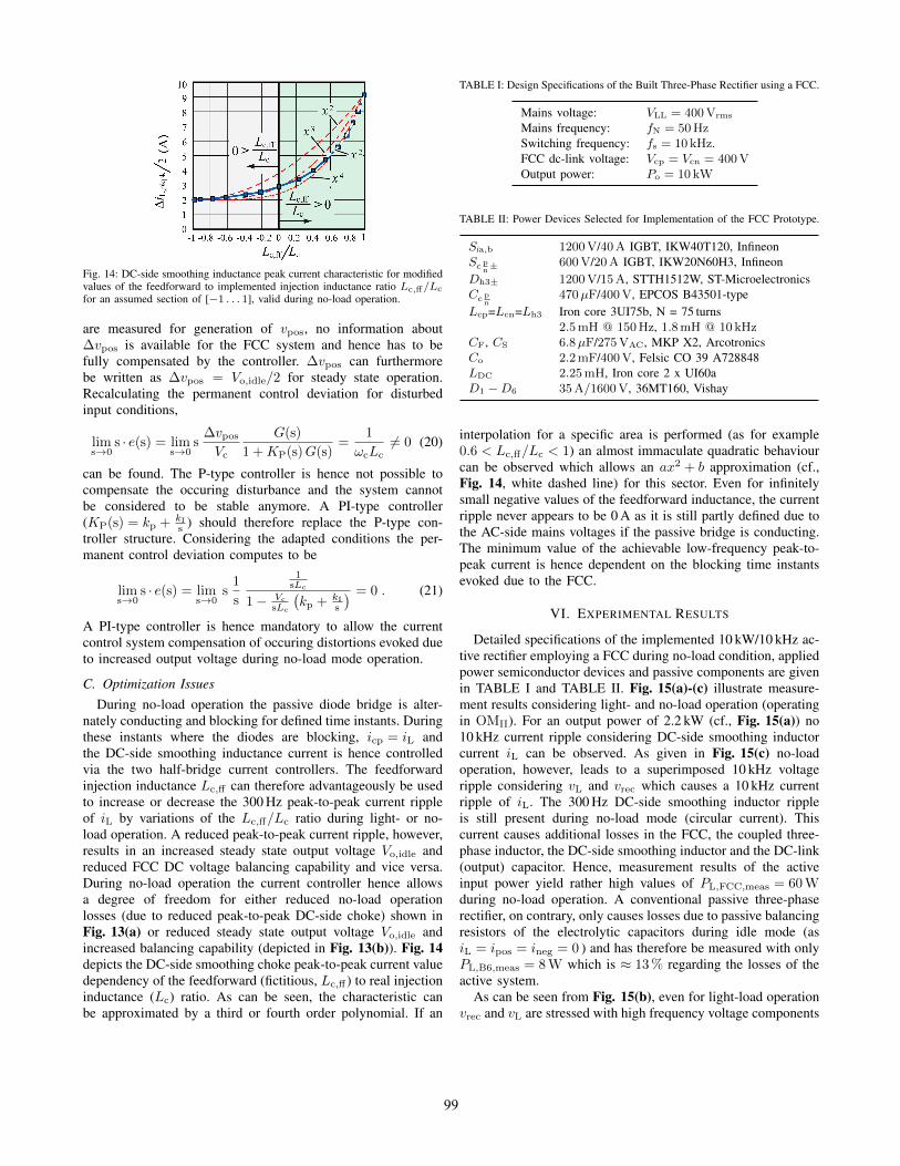
Fig. 14: DC-side smoothing inductance peak current characteristic for modifiedvalues of the feedforward to implemented injection inductance ratio Lc,ff/Lc
for an assumed section of [−1 . . . 1], valid during no-load operation.
are measured for generation of vpos, no information about∆vpos is available for the FCC system and hence has to befully compensated by the controller. ∆vpos can furthermorebe written as ∆vpos = Vo,idle/2 for steady state operation.Recalculating the permanent control deviation for disturbedinput conditions,
lims→0
s · e(s) = lims→0
s∆vpos
Vc
G(s)
1 +KP(s)G(s)=
1
ωcLc6= 0 (20)
can be found. The P-type controller is hence not possible tocompensate the occuring disturbance and the system cannotbe considered to be stable anymore. A PI-type controller(KP(s) = kp + kI
s ) should therefore replace the P-type con-troller structure. Considering the adapted conditions the per-manent control deviation computes to be
lims→0
s · e(s) = lims→0
s1
s
1sLc
1− Vc
sLc
(kp + kI
s
) = 0 . (21)
A PI-type controller is hence mandatory to allow the currentcontrol system compensation of occuring distortions evoked dueto increased output voltage during no-load mode operation.
C. Optimization IssuesDuring no-load operation the passive diode bridge is alter-
nately conducting and blocking for defined time instants. Duringthese instants where the diodes are blocking, icp = iL andthe DC-side smoothing inductance current is hence controlledvia the two half-bridge current controllers. The feedforwardinjection inductance Lc,ff can therefore advantageously be usedto increase or decrease the 300 Hz peak-to-peak current rippleof iL by variations of the Lc,ff/Lc ratio during light- or no-load operation. A reduced peak-to-peak current ripple, however,results in an increased steady state output voltage Vo,idle andreduced FCC DC voltage balancing capability and vice versa.During no-load operation the current controller hence allowsa degree of freedom for either reduced no-load operationlosses (due to reduced peak-to-peak DC-side choke) shown inFig. 13(a) or reduced steady state output voltage Vo,idle andincreased balancing capability (depicted in Fig. 13(b)). Fig. 14depicts the DC-side smoothing choke peak-to-peak current valuedependency of the feedforward (fictitious, Lc,ff ) to real injectioninductance (Lc) ratio. As can be seen, the characteristic canbe approximated by a third or fourth order polynomial. If an
TABLE I: Design Specifications of the Built Three-Phase Rectifier using a FCC.
Mains voltage: VLL = 400Vrms
Mains frequency: fN = 50HzSwitching frequency: fs = 10 kHz.FCC dc-link voltage: Vcp = Vcn = 400VOutput power: Po = 10 kW
TABLE II: Power Devices Selected for Implementation of the FCC Prototype.
Sia,b 1200V/40A IGBT, IKW40T120, InfineonSc p
n± 600V/20A IGBT, IKW20N60H3, Infineon
Dh3± 1200V/15A, STTH1512W, ST-MicroelectronicsCc p
n470µF/400V, EPCOS B43501-type
Lcp=Lcn=Lh3 Iron core 3UI75b, N = 75 turns2.5mH @ 150Hz, 1.8mH @ 10 kHz
CF, CS 6.8µF/275VAC, MKP X2, ArcotronicsCo 2.2mF/400V, Felsic CO 39 A728848LDC 2.25mH, Iron core 2 x UI60aD1 −D6 35A/1600V, 36MT160, Vishay
interpolation for a specific area is performed (as for example0.6 < Lc,ff/Lc < 1) an almost immaculate quadratic behaviourcan be observed which allows an ax2 + b approximation (cf.,Fig. 14, white dashed line) for this sector. Even for infinitelysmall negative values of the feedforward inductance, the currentripple never appears to be 0 A as it is still partly defined due tothe AC-side mains voltages if the passive bridge is conducting.The minimum value of the achievable low-frequency peak-to-peak current is hence dependent on the blocking time instantsevoked due to the FCC.
VI. EXPERIMENTAL RESULTS
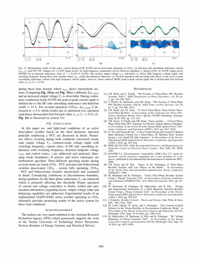
Detailed specifications of the implemented 10 kW/10 kHz ac-tive rectifier employing a FCC during no-load condition, appliedpower semiconductor devices and passive components are givenin TABLE I and TABLE II. Fig. 15(a)-(c) illustrate measure-ment results considering light- and no-load operation (operatingin OMII). For an output power of 2.2 kW (cf., Fig. 15(a)) no10 kHz current ripple considering DC-side smoothing inductorcurrent iL can be observed. As given in Fig. 15(c) no-loadoperation, however, leads to a superimposed 10 kHz voltageripple considering vL and vrec which causes a 10 kHz currentripple of iL. The 300 Hz DC-side smoothing inductor rippleis still present during no-load mode (circular current). Thiscurrent causes additional losses in the FCC, the coupled three-phase inductor, the DC-side smoothing inductor and the DC-link(output) capacitor. Hence, measurement results of the activeinput power yield rather high values of PL,FCC,meas = 60 Wduring no-load operation. A conventional passive three-phaserectifier, on contrary, only causes losses due to passive balancingresistors of the electrolytic capacitors during idle mode (asiL = ipos = ineg = 0 ) and has therefore be measured with onlyPL,B6,meas = 8 W which is ≈ 13 % regarding the losses of theactive system.
As can be seen from Fig. 15(b), even for light-load operationvrec and vL are stressed with high frequency voltage components
99
(a) (b) (c)
Fig. 15: Measurement results of the active system during CCM, ICOM and no-load mode operating in OMII. (a) Injection and smoothing inductance current(icp, iL) and FCC DC voltages for 1.33 kW output power. No high-frequency components can be observed regarding iL during CCM. (b) 0.8 kW output power(ICOM) for an injection inductance value of < 1.8mH @ 10 kHz. The rectifier output voltage vrec and hence vL shows high frequency voltage ripple withswitching frequency during those time instants where ipos yields discontinuous behaviour. (c) No-load operation and according side effects of the active system(circulating inductance current with high frequency current ripple), however, shows reduced 300 Hz peak-to-peak current ripple due to downscaled feed forwardvalue (Lc,ff/Lc ≈ 0.64).
during those time instants where ipos shows intermittent sec-tions. Comparing Fig. 15(a) and Fig. 15(c) a different ∆iL,pkpk
and an increased output voltage Vo is observable. During contin-uous conduction mode (CCM) the peak-to-peak current ripple isdefined due to the DC-side smoothing inductance and thereforeyields ≈ 18 A. For no-load operation (OMII) ∆iL,pkpk/2 de-creased to ≈ 6 A which results due to optimized loss operation(and hence downscaled feed forward value Lc,ff/Lc ≈ 0.64, cf.,Fig. 14) as discussed in section V.C.
VII. CONCLUSION
In this paper no- and light-load conditions of an activethree-phase rectifier based on the third harmonic injectionprinciple employing a FCC are discussed in detail. Numer-ous effects occuring during both conditions (increased steadystate output voltage Vo, common-mode voltage ripple withswitching frequency, current stress of DC-side smoothing in-ductance with switching frequency, distorted midpoint voltagevMN and control issues, ) are addressed and analyzed. Oper-ating mode boundaries of passive and active topologies arefurthermore specified. Three-different operating modes duringno-load mode are listed (OMI - FCC activated and bidirectionalswitches deactivated, OMII - system fully operating, OMIII
- FCC and bidirectional switches deactivated) and examinedin detail. Considering continuous to discontinuous boundary,design guidlines for the three-phase inductance Lc are enhancedwhich is primarily affecting this threshold. Proper operationof current and voltage controllers is finally verfied and opti-mization alternatives (regarding losses, output voltage value andbalancing capability) are addressed. Experimental results of animplemented 10 kW/10 kHz active rectifier operating in OMII
ultimately provides promising results of the active system forthese load conditions.
ACKNOWLEDGMENT
The authors are very much indebted to the Austrian ResearchPromotion Agency (FFG) which generously supports the workof the Vienna University of Technology Power ElectronicsSection (Institute of Energy Systems and Electrical Drives).
REFERENCES
[1] J.W. Kolar and T. Friedli, “The Essence of Three-Phase PFC RectifierSystems—Part I,” IEEE Transactions on Power Electronics, vol. 28, no.1, pp. 176–198, 2013.
[2] T. Friedli, M. Hartmann, and J.W. Kolar, “The Essence of Three-PhasePFC Rectifier Systems—Part II,” IEEE Trans. on Pow. Electron., vol. 29,no. 2, pp. 543–560, 2014.
[3] J.W. Kolar and F.C Zach, “A Novel Three-Phase Three-Switch Three-Level Pwm Rectifier,” in Proceedings of the Conference for Power Elec-tronics, Intelligent Motion, Power Quality (PCIM), Nuernberg, Germany,June 28-30 1994, pp. 125–138.
[4] T.B. Soeiro, T. Friedli, and J.W. Kolar, “Swiss rectifier — A Novel Three-Phase Buck-Type PFC Topology for Electric Vehicle Battery Charging,”in Proceedings of the Twenty-Seventh Annual IEEE Applied Power Elec-tronics Conference and Exposition (APEC), 2012, pp. 2617–2624.
[5] H. Yoo and Seung-Ki Sul, “A New Circuit Design and Control to ReduceInput Harmonic Current for a Three-Phase AC Machine Drive Systemhaving a very Small DC-link Capacitor,” in Proceedings of the Twenty-Fifth Annual IEEE Applied Power Electronics Conference and Exposition(APEC), 2010, pp. 611–618.
[6] IEEE Std 519-1992, IEEE Recommended Practices and Requirements forHarmonic Control in Electrical Power Systems, New York, NY: IEEE,1992.
[7] EC61000-3-2, Electromagnetic compatibility (EMC) Part 3-2: Limits forharmonic current emissions (equipment up to and including 16 A perphase), published by the International Electrotechnical Commission (IEC),2000.
[8] J.W. Kolar and H. Ertl, “Status of the Techniques of Three-PhaseRectifier Systems with Low Effects on the Mains,” in Proceedingsof the Twenty-First InternationalTelecommunication Energy Conference(INTELEC), 1999.
[9] M. Hartmann and R. Fehringer, “Active Three-Phase Rectifier SystemUsing a “Flying” Converter Cell,” in Proceedings of Energy Conferenceand Exhibition (ENERGYCON), 2012 IEEE International, 2012, pp. 82–89.
[10] M. Hartmann, R. Fehringer, M. Makoschitz, and H. Ertl, “Designand Experimental Verification of a Third Harmonic Injection RectifierCircuit Using a Flying Converter Cell,” in Proceedings of the Twenty-Ninth Annual IEEE Applied Power Electronics Conference and Exposition(APEC), 2014, pp. 920–927.
[11] J. Schaefer, Rectifier Circuits - Theory and Design, John Wiley & Sons,INC., New York, 1965.
[12] M. Leibl, Johann. W. Kolar, and J. Deuringer, “New Current ControlScheme for the Vienna Rectifier in Discontinuous Conduction Mode,” inProceedings of the Energy Conversion Congress and Exposition (ECCE),Pittsburgh, USA, Sept. 14-18 2014, pp. 1240–1247.
[13] M. Makoschitz, M. Hartmann, H. Ertl, and R. Fehringer, “DC VoltageBalancing of Flying Converter Cell,” in Proceedings of the EnergyConversion Congress and Exposition (ECCE), Pittsburgh, USA, Sept. 14-18 2014, pp. 4071–4078.
100