annealing effects on the mass diffusion of the cds/ito ... pdf... · difusividad m´asica de ... of...
TRANSCRIPT

INVESTIGACION REVISTA MEXICANA DE FISICA 52 (1) 15–19 FEBRERO 2006
Annealing effects on the mass diffusion of the CdS/ITO interface depositedby chemical bath deposition
A. Ordaz-Flores∗, P. Bartolo-Perez∗∗, R. Castro-Rodrıguez, and A.I. Oliva*Departamento de Fısica Aplicada, Centro de Investigacion y de Estudios Avanzados del IPN,
Apartado Postal 73 Cordemex, 97310 Merida, Yucatan, Mexico,e-mail: [email protected]
Recibido el 24 de enero de 2005; aceptado el 4 de noviembre de 2005
Cadmium sulphide thin films prepared by chemical bath deposition (CBD) were deposited on indium tin oxide (ITO) substrates with differentdeposition times (i.e. thickness) and characterised by their morphology and band gap energy. Samples were analysed as deposited and afterannealing at 90 and150◦C, in order to study the interface diffusion and its effects on the properties mentioned. Auger depth profiles wereused to determine the mass diffusivity coefficient in the CdS/ITO interface. The initial surface rms-roughness measured with AFM, as well asthe initial band gap energy, are reduced after the annealing process. We obtained very small diffusion coefficient values, around10−21 m2/s,for the different elements analysed in the interface.
Keywords: CdS/ITO interface; CBD; CdS films; ITO substrate; mass diffusion.
Capas delgadas de sulfuro de cadmio, preparadas por bano quımico, fueron depositadas sobre sustratos de ITO (oxido de estano impurificadocon indio) con diferentes tiempos de deposito (i.e. espesor) y caracterizadas en su morfologıa y en su brecha de energıa. Las muestras fueronanalizadas tanto recien depositadas como despues de ser recocidas a las temperaturas de 90 y150◦C, con el objetivo de estudiar la difusionen la interfaz CdS/ITO y sus efectos sobre las propiedades mencionadas. Con ayuda de los perfiles Auger, se determinaron los valores de ladifusividad masica de dicha interfaz. El valor inicial rms de la rugosidad superficial medida usando imagenes de fuerza atomica, ası como labrecha de energıa, se ven reducidos despues de los procesos de recocido. Se obtuvieron valores muy pequenos en los coeficientes de difusion,del orden de10−21 m2/s, para los diferentes elementos analizados en la interfaz.
Descriptores: Interfaz CdS/ITO; bano quımico; pelıculas delgadas de CdS; substrato ITO; difusion de masa.
PACS: 68.55.Nq; 79.60.Jv; 81.15.Lm; 82.80.Pv
1. Introduction
The technology for the promising high efficient CdS/CdTesolar cells requires a conductor substrate for improving. Forthis junction about16% solar conversion efficiency has beendemonstrated in the laboratory [1]. Indium tin oxide (ITO)films are usually deposited on glass substrate in order to con-trol their thickness and consequently their electrical conduc-tivity. Normally, ITO is used both as a conductor and as anelectrode to support the CdS thin film into the heterostructureCdTe/CdS/ITO/glass solar cell [2]. An interesting interfaceis formed when CdS is deposited by CBD technique on ITOsubstrate [3], which quality is related to the efficiency of theprepared solar cells. The interfaces qualities play an impor-tant role in facilitating the free electron flow through the com-plete solar cell to obtain high efficiency. Controlled changesin the properties of this interface can produce variations in theconductive properties of the semiconductor. Several effortstoward to study CdS/ITO [4, 5] and the CdS/CdTe [6] inter-faces have been reported in the literature. Some publishedworks predict the importance of the interface quality and theinterdiffusion mechanisms related to it. Annealing processesare normally made as attempts to reduce the intrinsic stressimproving the lattice mismatch and to produce longer trajec-tories for the free electrons for better electrical conductivity.The knowledge of the most appropriate temperature for de-positing the CdS onto the ITO substrates and the optimal an-
nealing process would make it possible to control the formedinterface, in order to improve the lattice mismatch and to in-crease the efficiency of the solar cell. The CBD technique hasproven to be an ideal technique to produce uniform and verythin films with low cost and simplicity. Films produced withthis technique are convenient to allow a good electric conduc-tivity and enough thickness such that the CdS material doesnot disappear when mixed with substrate in the interface (inour case, ITO).
2. Theory
In order to calculate the diffusion coefficientD, we choosethe linear semi-infinite diffusion model, by the geometry ofthe formed interface, and we take the results obtained from adepth profile concentration determined by the Auger electronspectroscopy (AES) technique. This is valid for the thin-filmconfiguration if we assumed that we can obtain accurate con-centration data at very short times [7]. For that, we need tosolve the temporal and one-dimensional Fick’s second law ofdiffusion given by:
∂C(x, t)∂t
= D∂2C(x, t)
∂2x2(1)
for the initial conditionsc(x,0)=0 andc(0,t)=c0 , and whichsolution is given by

16 A. ORDAZ-FLORES, P. BARTOLO-PEREZ, R. CASTRO-RODRIGUEZ, AND A.I. OLIVA
c
c0= erfc
(x
2√
Dt
)(2)
whereerfc(z)is the complimentary error function,x the depthof an element from the interface,t the deposition time,D thediffusion coefficient andz = x/(2
√Dt) . Values ofz are
tabulated forx, so by defining
m =1
2√
Dt(3)
and rewriting the solution (1) asc/c0 = erfc(mx), wecan find the corresponding linear regression to calculate theslopem, by means of which we can calculate the diffusioncoefficientD. The concentration profilec/c0 as a thickness(or time) function for a certain element is obtained from theAuger profile.
3. Experimental details
CdS thin films were deposited on 1×1 cm2 ITO substratescleaned with soap, acetone and isopropyl alcohol and rinsedwith distilled water between each step. CdS films were pre-pared by CBD technique with magnetic agitation. Detailsof the technique are widely described in the literature [8, 9].Briefly, the total volume (110 ml) of the chemical bath isformed by an aqueous solution containing the following mo-lar concentrations of each reactant: 0.02 M cadmium chloride(CdCl2), 0.5 M potassium hydroxide (KOH), 1.5 M ammo-nium nitrate (NH4NO3), and 0.2 M thiourea (CS[NH2]2) asa catalytic reagent. This is a widely used recipe for obtaininggood quality films [10]. The bath temperature was controlledat75± 1◦C by means of a Teflon covered type K thermocou-ple and connected to a home-made temperature controller,based on a CN4421TR-D1 Omega device with a solid staterelay. This temperature is widely used to obtain the CdS com-pound from the chemical components in order to achieve areasonable deposition rate. A lower bath temperature retardsthe CdS deposition rate, and a higher temperature produces ahigher evaporation of the chemical bath and an uncontrollabledeposition rate. The ITO substrates were supported by Teflonholders when they were immersed in the chemical bath. Filmdeposition starts when thiourea is added. Each sample holderand deposited film is retired one by one from the bath after10, 20, 30, 40, and 50 minutes of deposition time. The result-ing transparent and pale yellow films present bright surfacesand high adherence to the substrates, so that to eliminate theCdS film from one face of the substrate (for optical measure-ments) we need to use an HCl solution. The chemical bathsolution was agitated with a magnetic stirrer during deposi-tion. This method, used to produce high-quality CdS films, isvery useful for avoiding concentration gradients of the bathor colloids [8].
Annealing processes were carried out under clean con-ditions in a Fischer Scientific Vacuum Oven model 280, at
635 Torr. Annealing temperatures were measured with a mer-cury thermometer. All films were annealed for three hoursat two temperatures: 90◦ and 150◦C. These conditions werechosen as representative to produce clear diffusion in theCdS/ITO interface and higher than the chemical bath temper-ature during deposition. Optical and surface measurementswere made after films deposition and after each annealingprocess.
AFM images of films surfaces were obtained in the con-stant force mode with a high-resolution scanner (5×5 µm2).The mean rms-roughness values for three images of differ-ent sites of each film were obtained at atmospheric pressureand room temperature and an average value is reported forstatistics.
Film thickness was estimated from compositional depthprofiles performed by the Auger technique, with anESCA/SAM Perkin Elmer PHI 560 equipment yielding asputtering rate of about10 nm/min with Ar+ ions. The CdSfilm thickness was determined as the point where the Cdand S signals from the film mix with the Sn and In signalscoming from the ITO substrate. Thus, by knowing the sput-tering time of the depth profiles, the CdS film thickness canbe deduced. This technique was also used to measure at thesame time, the concentration of elements in the CdS/ITO in-terface while it is bombarding with Argon ions. Optical ab-sorption measurements were taken with a Jobin-Yvon/SpexH20-VIS spectrophotometer using a 250 W tungsten halogenlamp, with normal flux to the film surface. The wavelengthwas ranged from 300 to 800 nm. The resulting signal was re-ceived and processed with a Data Scan-2 controller coupledto a computer. Optical analysis were made after eliminat-ing the effect of the ITO/glass substrate from the depositedCdS/ITO/glass film. From here, we determined the CdS di-rect band gap energy (Eg) of CdS films by using the relation
α2 =1d2
ln2
[I0
I
]= A(E − Eg), (4)
with α being the absorption coefficient,d the film thickness,I andIo the transmitted and emitted light intensities, respec-tively, C a constant, andE the light energy.
4. Results and discussion
4.1. As-deposited films
The rms-roughness and the estimated thickness values of theas-deposited CdS films are shown in Table I. Film thicknessuncertainties are due to the standard deviations obtained fromfour profiles made on different sites of the sample. Values ofthe rms-roughness do not show an ordered behaviour withtime deposition maybe by the initial high ITO rms-roughness(15 nm); however, the lower values obtained in the reportedvalues indicates flatness films surfaces. The band gap ener-gies measured for the CdS/ITO samples are also included inTable I. The reported Eg values are measured with a 0.01 eVof uncertainty as estimated from the light intensity detector
Rev. Mex. Fıs. 52 (1) (2006) 15–19
ANNEALING EFFECTS ON THE MASS DIFFUSION OF THE CdS/ITO INTERFACE DEPOSITED BY CHEMICAL BATH DEPOSITION 17
and the monochromator device resolution. The highest valueof the band gap energy obtained for the thinnest film (∼ 8 nmfor 10 min as deposition time) is in good agreement with thequantum confinement effect of the electrons expected for thisthickness range [11]. Similar behaviour has been reportedfor our group during the formation of the band gap of theCdS films [12] during the first stage of growth. Values ofthe band gap reported for the thickest films correspond to thedirect band gap values of polycrystalline films measured atroom temperature (2.42− 2.45 eV). X-ray diffraction analy-sis show that CdS films present a cubic structure with a strongorientation in the (111) reflection peak and minor orientationsin the (220) and (311) peaks.
During the Auger depth profile analysis, we measured theconcentration of the Cd and S elements from the CdS film,and Sn and In from the ITO substrate. Oxygen from ITO wasnot recorded during the analysis because we considered thatit was not important in this study.
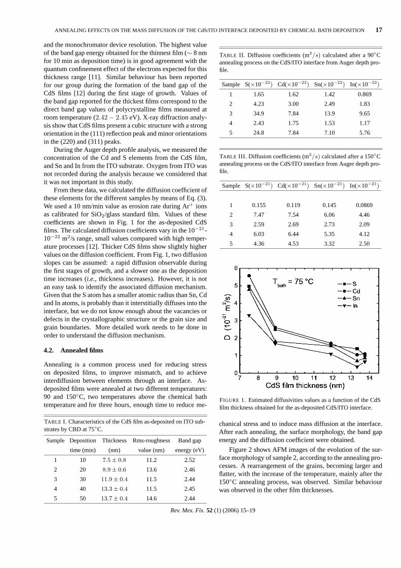
From these data, we calculated the diffusion coefficient ofthese elements for the different samples by means of Eq. (3).We used a 10 nm/min value as erosion rate during Ar+ ionsas calibrated for SiO2/glass standard film. Values of thesecoefficients are shown in Fig. 1 for the as-deposited CdSfilms. The calculated diffusion coefficients vary in the 10−21-10−22 m2/s range, small values compared with high temper-ature processes [12]. Thicker CdS films show slightly highervalues on the diffusion coefficient. From Fig. 1, two diffusionslopes can be assumed: a rapid diffusion observable duringthe first stages of growth, and a slower one as the depositiontime increases (i.e., thickness increases). However, it is notan easy task to identify the associated diffusion mechanism.Given that the S atom has a smaller atomic radius than Sn, Cdand In atoms, is probably than it interstitially diffuses into theinterface, but we do not know enough about the vacancies ordefects in the crystallographic structure or the grain size andgrain boundaries. More detailed work needs to be done inorder to understand the diffusion mechanism.
4.2. Annealed films
Annealing is a common process used for reducing stresson deposited films, to improve mismatch, and to achieveinterdiffusion between elements through an interface. As-deposited films were annealed at two different temperatures:90 and 150◦C, two temperatures above the chemical bathtemperature and for three hours, enough time to reduce me-
TABLE I. Characteristics of the CdS film as-deposited on ITO sub-strates by CBD at 75◦C.
Sample Deposition Thickness Rms-roughness Band gap
time (min) (nm) value (nm) energy (eV)
1 10 7.5± 0.8 11.2 2.52
2 20 8.9± 0.6 13.6 2.46
3 30 11.9± 0.4 11.5 2.44
4 40 13.3± 0.4 11.5 2.45
5 50 13.7± 0.4 14.6 2.44
TABLE II. Diffusion coefficients (m2/s) calculated after a 90◦Cannealing process on the CdS/ITO interface from Auger depth pro-file.
Sample S(×10−22) Cd(×10−22) Sn(×10−22) In(×10−22)
1 1.65 1.62 1.42 0.869
2 4.23 3.00 2.49 1.83
3 34.9 7.84 13.9 9.65
4 2.43 1.75 1.53 1.17
5 24.8 7.84 7.10 5.76
TABLE III. Diffusion coefficients (m2/s) calculated after a 150◦Cannealing process on the CdS/ITO interface from Auger depth pro-file.
Sample S(×10−21) Cd(×10−21) Sn(×10−21) In(×10−21)
1 0.155 0.119 0.145 0.0869
2 7.47 7.54 6.06 4.46
3 2.59 2.69 2.73 2.09
4 6.03 6.44 5.35 4.12
5 4.36 4.53 3.32 2.50
FIGURE 1. Estimated diffusivities values as a function of the CdSfilm thickness obtained for the as-deposited CdS/ITO interface.
chanical stress and to induce mass diffusion at the interface.After each annealing, the surface morphology, the band gapenergy and the diffusion coefficient were obtained.
Figure 2 shows AFM images of the evolution of the sur-face morphology of sample 2, according to the annealing pro-cesses. A rearrangement of the grains, becoming larger andflatter, with the increase of the temperature, mainly after the150◦C annealing process, was observed. Similar behaviourwas observed in the other film thicknesses.
Rev. Mex. Fıs. 52 (1) (2006) 15–19

18 A. ORDAZ-FLORES, P. BARTOLO-PEREZ, R. CASTRO-RODRIGUEZ, AND A.I. OLIVA
FIGURE 2. AFM images (1×1 µm2) of CdS thin films grown on ITO/glass deposited by CBD at 75◦C during 20 min; (a) as deposited, (b)after annealing at 90◦C, and (c) after annealing at 150◦C.
FIGURE 3. Behaviour of the band gap energy values with tem-perature. Corresponding temperatures are: deposition, 75◦C; firstannealing process (90◦C) and second annealing process (150◦C).Film thickness increases with the ample number according withTable I.
FIGURE 4. Concentration depth profile of the CdS/ITO interface ofsample 2 after annealing at 150◦C. The interface is marked betweenvertical lines.
The optical band gap energy of each film thickness weremeasured as-deposited and after each annealing process. Fig-ure 3 shows the results. Higher annealing temperatures causea decrement in the band gap energy value in all films. Pre-sumably, during the annealing process, atoms rearrange tomore energetic and suitable positions on the valence band.In this way, the photo-current can be increased by the longermean free path of electrons, so that less energy is needed foran electron to jump to the conduction band.
FIGURE 5. Changes of the diffusivity values after from annealingprocess at 90 and 150◦C on the CdS/ITO interface. Film depositiontime. (a) sample 2 (20 min); (b) sample 5 (50 min).
Rms-roughness values show an almost constant be-haviour on film surface before and after the annealing pro-cesses, with no tendencies to increase or diminish in anycase. As can be deduced from the AFM images, the annealingprocess is not a parameter that could affect the surface rms-roughness value behaviour in this thickness range. However,grain size on the film surface is observed clearly to increasewith the annealing treatment. According to the literature, mi-nor grain size produces a larger diffusion velocity because ofthe larger space between grains if the diffusion is producedby grain boundaries.
Auger depth profiles are normally used for chemical anal-ysis. We used this technique for film thickness determination,
Rev. Mex. Fıs. 52 (1) (2006) 15–19

ANNEALING EFFECTS ON THE MASS DIFFUSION OF THE CdS/ITO INTERFACE DEPOSITED BY CHEMICAL BATH DEPOSITION 19
given the small thickness produced by the small depositiontime. Film thickness proved difficult to calculate with thistechnique after annealing, because of the larger grain size; forthat reason, the thickness value considered in this work as ref-erence for further calculations is the value measured for theas-deposited films. Figure 4 shows a typical Auger depth pro-file obtained for the CdS/ITO interface. Profiles of the mainelements mixed in the interface are monitored. Concentrationprofiles obtained for the Auger technique correspond also forsample 2, but similar behaviour was obtained for the otherfilm thickness. From these profiles, and using the equationsdiscussed in Sec. 2, we calculated the diffusion coefficient Dfor each element after each annealing process.
Diffusion coefficient values calculated for the differentelements involved on the CdS/ITO interface were found torange between 10−21 and 10−22 m2/s after the first anneal-ing process at 90◦C was completed. A slower diffusion pro-cess is observed as compared with the as-deposited films, sothat we believe that a different diffusion mechanism couldbe involved. The annealing process causes the movement ofatoms because of the originated rearrangements so that grainboundary diffusion and interstitial diffusion could the mostprobable processes involved. In all cases, the S stands outto be more easily diffusible than the other elements by thehigher values calculated in all cases (see Table II).
An important point to regard is that the deposited filmduring 10 min, presents the lowest diffusion coefficients inall cases. Given that is the thinnest thickness (8 nm), it hasless material to diffuse, as compared with the thickest films,the crystalline structure is forming yet and quantum effectscan be given.
After the second annealing process at 150◦C (Table III),the diffusion rates are, in general, faster than the first anneal-ing. This can be better seen from the plots shown in Fig. 5.Grain boundary and interstitially diffusion can be the mostappropriate diffusion mechanism after this process. However,the effect of second annealing process was higher diffusioncoefficients and a wider interface. Contrarily to the first an-nealing, the wideness of the interface changed considerablyafter the 150◦C annealing process. The annealing at 90◦Cdoes not seem to make interesting changes in the morphol-ogy nor the diffusion coefficients, but it is enough to appreci-ate changes in the band gap. Then, high annealing tempera-tures stand out to be performed in further studies focused ondiffusivity and morphology.
Dispersion on the diffusivity values described on Ta-bles II and III, are due to the surface roughness condition ofthe analysed samples. By the local characteristic of the Augertechnique, the depth profile analysis will depend on the sitewhen the beam hits. Given that film roughness changes withannealing temperature, then, depth profile can change fromsite to site on sample, and consequently, the detected ele-ments (S, Cd, In, and Sn) can vary on concentration. How-ever, the implemented method to calculate the coefficient ofdiffusivity can be useful to study and quantify diffusion onthe interfaces of bimaterial layers.
Acknowledgments
Authors thank to Emilio Corona, Wilian Cauich, O. Ceh andVıctor Rejon for their technical support. This work was sup-ported by CONACYT (Mexico) under projects 38667-E and38480-E.
∗. Tesista de Ingenierıa Fısica de la Facultad de Ingenierıa de laUADY.
∗∗. On leave on the Programa de Corrosion del Golfo de Mexicode la UAC.
1. J. Britt and C. Ferekides,Appl. Phys. Lett.62 (2001) 2851.
2. Dieter Bonnet,Cadmium telluride solar cells. In Clean electric-ity from photovoltaics, Mary D. Archer y Robert Hill, (Editors).(Imperial College Press, London, 2001).
3. A.I. Oliva et al., Appl. Surf. Sci. 148(1999) 42.
4. A. Martel et al., Phys. Stat. Sol. b220(2000) 261.
5. K.D. Dobson, I. Visoly-Fisher, G. Hodes, and D. Cahen,Sol.Energy Mat.& Sol. Cells62 (2000) 295.
6. B.E. McCandeless, M.G. Engelmann, and R.W. Brikmire,J.Appl. Phys.89 (2001) 988.
7. M.E. Glicksman,Diffusion in Solids(John Wiley & Sons. 2000)Chapter 3, p. 472.
8. J.M. Dona and J. Herrero,J. Electrochem. Soc. 144 (1997)4081.
9. D. Lincot and R. Ortega-Borges,J. Electrochem. Soc. 140(1993) 3464.
10. J.M. Dona and J. Herrero,J. Electrochem. Soc. 144 (1997)4091.
11. K.K. Nanda, S.N. Sarangui, S. Mohantay, and S.N. Sahu.ThinSolid Films322(1998) 21.
12. A.I. Oliva, O. Solıs, R. Castro-Rodrıguez, and P. Quintana,ThinSolid Films391(2001) 28.
Rev. Mex. Fıs. 52 (1) (2006) 15–19