anp-32 practical layout guidelines for power designs · anp-32 practical layout guidelines for...
TRANSCRIPT

PPoowweerrXXRR
AANNPP--3322 PPrraaccttiiccaall LLaayyoouutt GGuuiiddeelliinneess ffoorr PPoowweerrXXRR DDeessiiggnnss October 2012 Rev. 1.1.0
Exar Corporation www.exar.com 48720 Kato Road, Fremont CA 94538, USA Tel. +1 510 668-7000 – Fax. +1 510 668-7001
GENERAL DESCRIPTION Proper layout of the PowerXR controller and nearby components follows all traditional best practices of power electronics converter designs.
In short this means that the guiding principles discussed next will deal heavily with:
• Minimizing the surface area of the switch node to avoid capacitive coupling of noise
• Minimizing the loop areas of the gate drives
• Minimizing the loop areas of the boot strap charging circuits
• Minimizing the ON and OFF current loops of the synchronous buck circuit.
• Proper design of ground planes around the PowerXR controller.
Finally there will be a discussion on the proper hookup of the remaining digital and analog pins on the PowerXR controller.
LAYOUT GUIDELINES CHECKLIST o DO NOT USE AUTOROUTING
o Minimize the switch node area
o Minimize the area enclosed by the ON and OFF power path loops
o Minimize the area enclosed by the gate drive current path loops
o Keep the feedback routing clear of noise sources like the switch node
o Keep the power ground planes isolated except for connections to system ground at output capacitor
o MOSFETs and inductors need to be coupled to enough copper to dissipate the heat generated
o PowerXR controller needs to be coupled to enough exposed ground copper to dissipate the heat generated
o Tight bypassing of VDD and GPIO pins
3-CHANNEL POWERXR LAYOUT EXAMPLE
Top Layer of a Final XRP7713 Based Layout

PPoowweerrXXRR
AANNPP--3322 PPrraaccttiiccaall LLaayyoouutt GGuuiiddeelliinneess ffoorr PPoowweerrXXRR DDeessiiggnnss
© 2012 Exar Corporation 2/15 Rev. 1.1.0
SYNCHRONOUS BUCK FUNCTION
Figure #1 – Synchronous Buck Topology
The synchronous buck regulator is comprised of two circuits formed by the closing of one or the other of a high and low side MOSFET. The high side MOSFET is the main switch and when being driven will create the circuit hereafter referred to as the ON state.
The low side MOSFET is the circuit element that provides a path for the inductor current when the high side MOSFET turns off. Being a synchronous converter this element is a MOSFET. Non-synchronous converters merely use a diode. From here on the circuit created by this MOSFET being driven will be referred to as the OFF state.
LAYOUT GUIDELINES IN DEPTH
LAYOUT GUIDELINE #1 – MINIMIZE THE SWITCH NODE The switch node is the net connecting Q_HIGH, Q_LOW, and L together. This net has a high dV/dt. The concern around a high dV/dt net is that it can capacitive couple its square wave signal onto conductors that pass above, below, or laterally (if close enough).
Capacitive coupling is directly related to surface area so the bigger the node the more pronounced the effect. The trade off to just making the node as small as possible is that Q_LOW is going to be generating heat and the drain of Q_LOW is the path conducting the heat away from Q_LOW. Therefore there is a balance between making the net large enough to dissipate heat and small enough to not radiate too much noise.
Calculations can be made to determine the amount of heat to be dissipated by Q_LOW to help with this determination. To get assistance in this regard please refer to [the PowerXR Power Optimizer and/or Power Architect] the PowerXR datasheet section on MOSFET component selection or seek the help of your regional PowerXR FAE.
Obviously the best design is going to be a tradeoff between surface area and noise requirements. Figures 2 and 3 are a couple of examples of layouts that successfully satisfy the necessary balance.

PPoowweerrXXRR
AANNPP--3322 PPrraaccttiiccaall LLaayyoouutt GGuuiiddeelliinneess ffoorr PPoowweerrXXRR DDeessiiggnnss
© 2012 Exar Corporation 3/15 Rev. 1.1.0
Figure #2 – Top Layer Design for Dual FET Figure #3 – Top Layer Design for Single FET
The last point to consider is the need for multilayer boards to avoid routing anything directly below the switch node or the associated inductor. The only acceptable components to place underneath the inductor and/or switch node are the MOSFETs themselves. Ground planes covering the whole board that are interleaved with the switch node actually can have a beneficial effect in that they turn the switch node from a monopole noise source to a bi-pole noise source. Most often the switch node is mirrored on every layer and tied via stitching vias. This is done to help with adding thermal mass and spreading heat to the surface on the back of the board for better thermal dissipation. The need for this and the degree of application are tied to the amount of heat to be removed. Below are some images demonstrating these techniques.
Figure #4 – Multiple layers showing the mirrored Switch Node and via stitching to spread heat
Note that these switch nodes are not immediately next to other switch nodes, any critical DC signal, or the controller. When doing component floor planning keep in mind that even the best designs can cause noise if a critical signal is placed next to the switch node. If possible get these along the edge of the board away from everything else. Otherwise don’t put any critical signals right next to them.

PPoowweerrXXRR
AANNPP--3322 PPrraaccttiiccaall LLaayyoouutt GGuuiiddeelliinneess ffoorr PPoowweerrXXRR DDeessiiggnnss
© 2012 Exar Corporation 4/15 Rev. 1.1.0
LAYOUT GUIDELINE #2 – MINIMIZE THE POWER PATH CURRENT LOOPS The second way to generate electromagnetic noise in a switch mode power supply besides capacitive coupling is driving a magnetic field with a large current loop. Current traveling through components will complete the circuit through a return path. This complete circuit will radiate a magnetic field in proportion to the area enclosed by the loop and the strength of the current travelling the loop at a right angle to the plane of the loop. Obviously in a switch mode power supply these loops are of most concern with the power components. There are however also loops formed by the gate drives, bootstrap circuits, and controller. There will be more on these later.
Figure #5 – ON State Current Loop Figure #6 – Gerber of a Dual MOSFET layout with arrows indicating ON State current loop
On State Power Path Current Loop
First, we’ll focus on the ON state. As depicted in Figure #5, the current travels from C_IN through the MOSFET Q_HIGH into the inductor L and ends its trip with the capacitor C_OUT. Then the current returns through a ground connection between the capacitors.
It’s important that the components that form this loop create the loop so that the current travels a continuous clockwise or counterclockwise path. The direction is not as important as the fact that the loop does form a “figure eight”. The reason for this is to create a predictable magnetic field in only one direction. Figure #6 uses yellow arrows to indicate the current loop created by the ON State. Take notice that the return path from C_OUT to C_IN is made through a plane connection in light blue on another layer.
Most often it is not possible to get C_IN and C_OUT anodes physically close together. The reason for this being that the MOSFETs often need to be placed in such a way around the inductors so as to prevent ideal capacitor placement. The next best alternative is to tie the two capacitors together via a dedicated ground plane. This is perfectly acceptable and even desirable. In a higher current design, say >8Amps, Figure #6 would have been modified allow the ground to connect directly without vias by using vias on the gate drive traces.
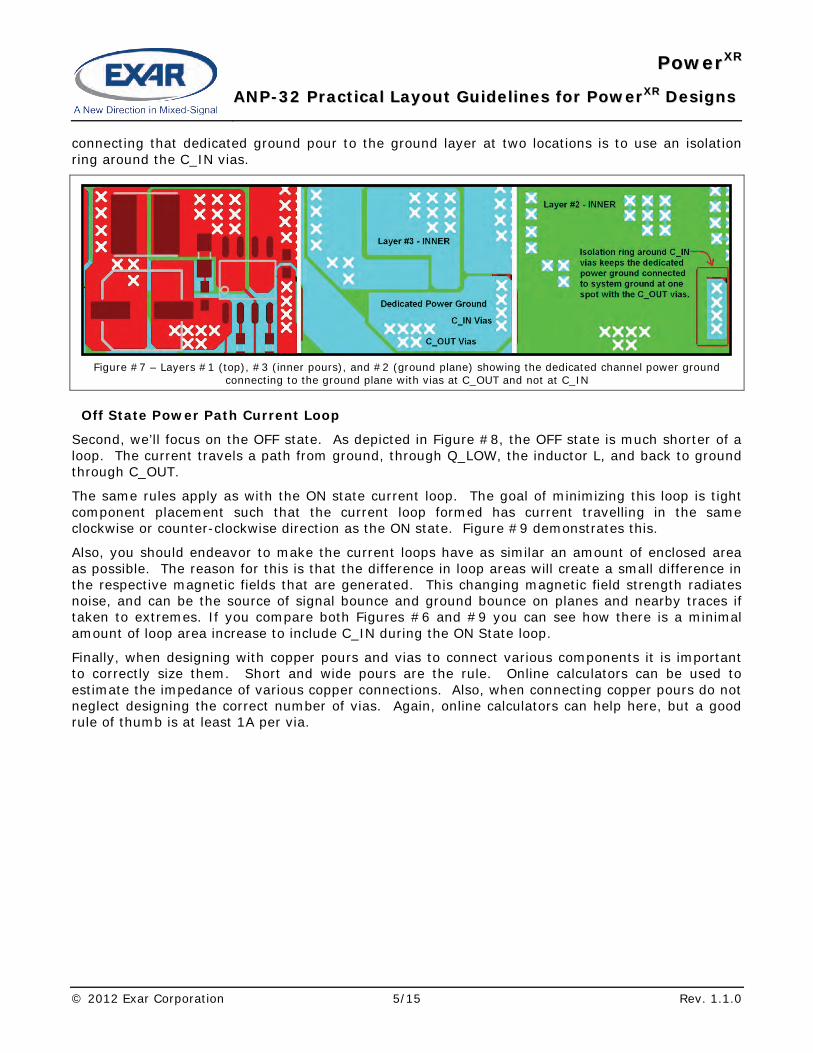
However, there is one common mistake that should be avoided. This ground plane needs to be its own dedicated pour with only a single physical connection to the board level ground plane at the output capacitor C_OUT. The best location for this ground plane is on the bottom layer or the internal power distribution layer as routing allows.
Figure #7 below shows how an inner layer (Layer #3 in Light Blue here) can be used with the appropriate number of stitching vias to tie C_IN and C_OUT together. As in Figure #6 there most likely won’t be a way to make the connection on the component level. So the best way to avoid
PPoowweerrXXRR
AANNPP--3322 PPrraaccttiiccaall LLaayyoouutt GGuuiiddeelliinneess ffoorr PPoowweerrXXRR DDeessiiggnnss
© 2012 Exar Corporation 5/15 Rev. 1.1.0
connecting that dedicated ground pour to the ground layer at two locations is to use an isolation ring around the C_IN vias.
Figure #7 – Layers #1 (top), #3 (inner pours), and #2 (ground plane) showing the dedicated channel power ground connecting to the ground plane with vias at C_OUT and not at C_IN
Off State Power Path Current Loop
Second, we’ll focus on the OFF state. As depicted in Figure #8, the OFF state is much shorter of a loop. The current travels a path from ground, through Q_LOW, the inductor L, and back to ground through C_OUT.
The same rules apply as with the ON state current loop. The goal of minimizing this loop is tight component placement such that the current loop formed has current travelling in the same clockwise or counter-clockwise direction as the ON state. Figure #9 demonstrates this.
Also, you should endeavor to make the current loops have as similar an amount of enclosed area as possible. The reason for this is that the difference in loop areas will create a small difference in the respective magnetic fields that are generated. This changing magnetic field strength radiates noise, and can be the source of signal bounce and ground bounce on planes and nearby traces if taken to extremes. If you compare both Figures #6 and #9 you can see how there is a minimal amount of loop area increase to include C_IN during the ON State loop.
Finally, when designing with copper pours and vias to connect various components it is important to correctly size them. Short and wide pours are the rule. Online calculators can be used to estimate the impedance of various copper connections. Also, when connecting copper pours do not neglect designing the correct number of vias. Again, online calculators can help here, but a good rule of thumb is at least 1A per via.

PPoowweerrXXRR
AANNPP--3322 PPrraaccttiiccaall LLaayyoouutt GGuuiiddeelliinneess ffoorr PPoowweerrXXRR DDeessiiggnnss
© 2012 Exar Corporation 6/15 Rev. 1.1.0
Figure #8 – OFF State Current Loop Figure #9 – Gerbers of a Dual MOSFET layout with arrows
indicating OFF State current loop
LAYOUT GUIDELINE #3 – MINIMIZING CURRENT LOOPS FOR THE GATE DRIVERS Now that you are familiar with current loops and their associated best layout practices let’s talk about the less powerful, but no less important gate drive current loops. The PowerXR controllers have on-board gate drivers and power sources which is helpful with layout. A switch-mode power supply relies on gate drivers to quickly charge and discharge MOSFET gate oxide. As a result there are brief but powerful current pulses traveling the path to the gate and back as you can see below in Figures #10-14.
Figure #10 – Current Loop for Turning ON Q_HIGH Figure #11 – Current Loop for Turning OFF Q_HIGH
Figure #12 – Current Loop for Turning ON Q_LOW Figure #13 – Current Loop for Turning OFF Q_LOW

PPoowweerrXXRR
AANNPP--3322 PPrraaccttiiccaall LLaayyoouutt GGuuiiddeelliinneess ffoorr PPoowweerrXXRR DDeessiiggnnss
© 2012 Exar Corporation 7/15 Rev. 1.1.0
Figure #14 – Current Loop for Charging the Boost Capacitor for the High Side Gate Driver

PPoowweerrXXRR
AANNPP--3322 PPrraaccttiiccaall LLaayyoouutt GGuuiiddeelliinneess ffoorr PPoowweerrXXRR DDeessiiggnnss
© 2012 Exar Corporation 8/15 Rev. 1.1.0
Q_LOW Gate Drive Loops
PowerXR controllers have a very fortuitous pin out for direct fan-out to MOSFETs. We’ll start with discussing the easiest current loops – those for Q_LOW. GL and PGND are adjacent pins as are LX, GH, and BST. Note that the importance of properly routing PGND has prompted Exar to change the name of this pin on the XRP7724 to GL_RTN.
As you can see in Figures #12 and #13 Q_LOW has a very simple circuit path. The simpler of the two is Figure #13 which shows the Q_LOW turn OFF loop travelling two single etches.
The more complex path is the Q_LOW turn ON loop. Gate drive current during turn ON travels from GL to Q_LOW and returns through the source pin to PGND and the ground plane. Do not tie the PGND pin on the controller to the ground plane directly for the return path. If PGND is being routed with vias then isolate them with guard rings to prevent accidental connection to the ground plane. That is, the PGND pins should only connect to the ground plane for the system at the Q_LOW source pin.
Now at this point you might be saying, “A-ha! Where is the capacitor completing the loop from the gate driver’s power supply to PGND?” Well good for you. There is indeed a power connection at VCCD for powering the onboard gate drivers for all four channels. There is also a ceramic capacitor there to ground labeled C_DRV which can be seen in Figures #12 & #14.
Thus in designs done with the PowerXR controllers the low side gate drive turn ON return current (Figure #12) will travel into the Q_LOW source pin and then into the ground plane connecting the VCCD capacitor. This is the only return path that travels into the system ground plane.
What little noise is generated on the gate drive power rail from all the channels is filtered before returning to VCCA by the use of a PI filter formed by connecting a C-R-C network between VCCA (the source of the 5V gate drive) and VCCD (the input for the gate drive power). This is recommended and can be seen below in Figure #15. Suggested values are 4.7uF X5R capacitors and 4.99Ω resistor.
Figure #15 – Capacitor – Resistor – Capacitor filter between VCCA (pin29) and VCCD (pin18) on the XRP7713 three channel controller

PPoowweerrXXRR
AANNPP--3322 PPrraaccttiiccaall LLaayyoouutt GGuuiiddeelliinneess ffoorr PPoowweerrXXRR DDeessiiggnnss
© 2012 Exar Corporation 9/15 Rev. 1.1.0
Q_HIGH Gate Drive Current Loops
Next of interest is the gate drive loop for Q_HIGH. As you can see in Figures #10 & #11 this loop is a little more interesting. For the moment we’ll disregard the bootstrap charging loop and talk just about the gate drive path.
The GH drive signal returns to the driver circuitry from the Q_HIGH source through the LX pin. This is an easy loop and is easy to route because LX and GH are adjacent to PGND and GL on the controller for each channel. These nets therefore can and should be routed as a nice bus out to the power circuitry.
Now, again you might say, “Where’s the gate driver capacitor?” It’s there. It’s the capacitor C_BST connecting BST to LX. The interesting thing about N-Channel MOSFETs is that they need a gate drive with a higher potential than the source which means that a synchronous buck needs a charge pump to generate a voltage higher than Vin. That’s the point of the diode D_BST and capacitor C_BST shown in Figures #10 and #14. The XRP7724 has integrated the diode D_BST.
The components D_BST and C_BST are best located closely to the controller and not the power components for the tightest possible loop (Figure #14).
There are actually three loops for this circuitry. The first loop is during the ON state turn ON (Figure #10) when energy is pulled out of C_BST into the BST pin, then fed to the MOSFET through GH and returning via LX.
The second loop is during the ON state turn OFF (Figure #11) where GH discharges the gate oxide of Q_HIGH and the return path is from LX to the Q_HIGH source.
The third loop is during the OFF state (Figure #14) when the LX net is shorted to PGND through Q_LOW being turned ON. During this state power from VCCD travels through the forward biased D_BST to charge C_BST. This is another hard loop to draw with four controllers on one chip and is a little reminiscent of the low side gate drive return path to the VCCD capacitor. Never fear, if you followed good layout practice for routing GL and PGND this will take care of itself. Also note that the XRP7724 has two VCCD pins for improved performance.
Summary of Gate Drive Current Loop Recommendations
Figure #16 – Highlighted nets showing a bus routing on the power stage gate drivers for one of the three channels

PPoowweerrXXRR
AANNPP--3322 PPrraaccttiiccaall LLaayyoouutt GGuuiiddeelliinneess ffoorr PPoowweerrXXRR DDeessiiggnnss
© 2012 Exar Corporation 10/15 Rev. 1.1.0
So in summary, when it’s all said and done you should have a layout such as shown in Figure #16 where all the connections involved in gate drive (PGND, GL, LX, GH, BST) are tightly routed as a bus. Always route these traces as a bus. Channels 3 (and 4 for the four channel PowerXR devices) are mirrored on the controller, and you may find it necessary to use vias to route tightly to the MOSFETs. This is perfectly normal and usually required.
The VCCD connection to C_BST, D_BST, and the BST pins should be routed with 20mil+ traces.
Also of serious note is the dual functionality of a tightly coupled LX and PGND pin. The PowerXR controllers look at the signal across LX and PGND during the OFF state to get an accurate measure of voltage drop across the Q_LOW Rds_on resistance. This is essential for good peak current measurement, and the routing can be thought of in the same way as a good Kelvin sense connection across a current sense resistor.
Advanced gate drive layout techniques
Gate drive routing is a critical component of making all manner of design compromises in layout work out for the best. If done improperly it can result in horrible EMI problems, poor regulation, nuisance over current faulting, and even damage.
One element of good routing is shielding the rest of the circuit board nets (like VOUT feedback) from the power supply. The best practice is to make use of DC voltage nets forming pours and etch to wrap around the gate drive bus routing. Acceptable nets are various GNDs, Vin, and Vout.
Figure #17 – Example of a good use of a ground plane below the gate drive bus routing to shield internal traces from the gate drive
Figure #18 – Example of a great combination of two DC planes being used to shield other traces from the gate drive
GH# LX# GL# PGND
GND
GND or Power Plane GREAT BUS VOUT#
LX# GL# PGND# VOUT#
GND
GH# GOOD BUS

PPoowweerrXXRR
AANNPP--3322 PPrraaccttiiccaall LLaayyoouutt GGuuiiddeelliinneess ffoorr PPoowweerrXXRR DDeessiiggnnss
© 2012 Exar Corporation 11/15 Rev. 1.1.0
LAYOUT GUIDELINE #4 – FEEDBACK ROUTING The PowerXR controllers have a common mode feedback range up to 5.1V (XRP7724 extends this to 5.5V). Therefore the feedback connection pins VOUT1-4 typically connect directly to the output nets.
The ideal routing is a path that takes the signal far from any switch nodes or inductors that could capacitively or magnetically couple noise to the controller.
If the output voltage is greater than 5.1V and a resistor divider is being used, then the ideal location of the divider is at the VOUT pin. Placing it close to the output capacitor instead introduces high impedance at the wrong end of the trace that could allow noise to show up with a strong signal at the feedback pin just as the sample and hold operation of the A2D begins.
For this reason it’s common practice to put a ceramic decoupling capacitor to AGND on the VOUT pins. The only exception is if a voltage divider is used. In this case there won’t be a decoupling capacitor on the pin at all because it’d corrupt the signal due to the RC filter formed between the capacitor and the top of the divider. A decoupling capacitor located across the entire resistor divider however is recommended. It is the next best thing since the resistor divider and capacitor should already be located very close to the VOUT pin.
Figure #19 shows a highlighted trace of VOUT3 travelling directly from the output capacitor to the VOUT3 pin. It touches a decoupling capacitor before the controller to guarantee the entire net is low impedance and unlikely to pick up any noise. And notice that it avoids passing near the switch node, and only travels alongside the gate drive routing bus (specifically PGND) for a very short and acceptable distance.
Figure #19 – Example of how to route feedback to the VOUT pins from the output capacitors

PPoowweerrXXRR
AANNPP--3322 PPrraaccttiiccaall LLaayyoouutt GGuuiiddeelliinneess ffoorr PPoowweerrXXRR DDeessiiggnnss
© 2012 Exar Corporation 12/15 Rev. 1.1.0
LAYOUT GUIDELINE #5 – PLANE LAYER DESIGN The best designs for the PowerXR controller are going to be four or more layers. With great care and ample board space proper designs can be done with only two layers. However, modern designs that can best make use of the PowerXR controller are mostly achieved with 4+ layers. So that being said the traditional stackup for a PowerXR design is the following:
Layer #1 –Top side components, high current pour connections, and most gate drive bus routing.
Layer #2 – Plane connections to power distribution for each output and input and dedicated channel grounds (as discussed in the power component current loop section).
Layer #3 – Usually the board ground
Layer #4 – Routing between layers, gate drive bus routing, and bottom side component placement
If it is expected that the controller will be running hot due to a high switching frequency and big MOSFETs or heavy use of the standby regulator, then there is a thermal reason for adding as much ground copper as possible around the controller. The easiest way is to drop several vias on the thermal pad of the controller and stitch it to every layer filling any space under the controller with ground copper. Ultimately heat is dissipated by exposed surface area. So if an exceptionally hot design is intended, then do your best to keep components out from directly underneath the controller on the back side of the board. The result will give you plenty of room to create a very large copper ground pour to stitch the controller to on the bottom layer.
Good use of vias may reduce RθJA by 15∼25%. Use 0.33 mm diameter vias if possible - especially for packages with a small exposed pad. Place the thermal vias near the periphery of the exposed thermal pad if the maximum number of vias is not applicable. Figure #20 shows the point of diminishing returns for a 2.1 x 2.1mm die tends to begin with about 5 or 6 stitching vias.
Figure #20 – Chart showing improvement in junction to ambient temperature resistance versus the number of vias for two different die sizes.
Figure #20 demonstrates a simulated thermal junction to ambient resistance for two die sizes using different numbers and patterns of stitching vias to couple the package decal with a ground plane on the back side of the board.

PPoowweerrXXRR
AANNPP--3322 PPrraaccttiiccaall LLaayyoouutt GGuuiiddeelliinneess ffoorr PPoowweerrXXRR DDeessiiggnnss
© 2012 Exar Corporation 13/15 Rev. 1.1.0
Power and Grounding Connections
The PowerXR controller has three general ground categories: DGND, AGND, and PGND(s) (GL_RTN in the case of the XRP7724). The PGNDs have been discussed in detail already. However the other grounds deserve some instruction.
AGND is connected to the thermal pad as well as a pin. AGND is the return for the entire analog to digital converter circuitry inside the controller as well as the linear regulators.
DGND is brought out to a single pin and is the return for the digital circuitry.
AGND and DGND are brought out to adjacent pins and should be connected together along with the thermal pad with as short a trace as possible. Ideally the thermal pad has stitching vias to deal with heat build up. These vias will serve as the single point connection to the ground plane or to a dedicated controller ground (which was the case for the design from which the images of this document were gathered). For the XRP7724, the DGND should connect to the exposed pad AGND.
The AVDD and DVDD pins should also have decoupling capacitors that are connected with as short a trace as possible to these pins and their corresponding AGND and DGND pins.
The standby linear regulator LDOOUT (XRP7724 LDO3_3) – if used – must have a compensation capacitor that needs to be placed near the controller and decoupled to AGND.
The analog linear regulator VCCA (XRP7724 LDO5) also requires a compensation capacitor that needs to be placed near the controller and decoupled to AGND. The capacitor also forms part of the filter between VCCA and VCCD (Figure #15).

PPoowweerrXXRR
AANNPP--3322 PPrraaccttiiccaall LLaayyoouutt GGuuiiddeelliinneess ffoorr PPoowweerrXXRR DDeessiiggnnss
© 2012 Exar Corporation 14/15 Rev. 1.1.0
LAYOUT GUIDELINES #6 – MISCELLANEOUS ATTENTIONS 1) Keep all decoupling capacitors close to the controller especially those connected to VCCA,
AVDD, DVDD, and Enable. For the XRP7724 this would include LDO3_3, LDO5, CPLL, DVDD, and Enable.
2) It is common practice to put resistors (usually 0 ohm at first) in series with the Gate Drives and BST pins. This is for slowing the edges of the switching transitions of MOSFETs. Increasing the values of the resistors can solve many EMI problems that may arise at the expense of some efficiency. Its good practice to add them to a first spin until the EMI pre-compliance testing can be completed and their need (or lack of) is confirmed. There placement is not as critical as long as they do not interrupt the tight bus routing talked about above in the gate drive current loop section.
3) It is also common practice to add an RC snubber from LX to GND to snub the switching spike that results from the charging and oscillation of any leakage inductance present in the inductor and routing. These pads should be placed directly across the Q_LOW Drain and Source. An example can be seen in Figure #21. Our recommendation is to not populate these unless required by EMI concerns.
4) When floor planning a design that will force at least some channels to be several inches from the controller, then place the highest current channels closest to the controller. This will prevent the heavier gate drive currents from being driven further than necessary and potentially forcing compromises with EMI and efficiency.
5) Place the controller and its highest current power circuitry closest to the heaviest load in need of the most accurate output voltages. Then use wide and thick plane routing to distribute the rest of the rails throughout the PCB as needed.
Figure #21 – Recommended snubber location is directly across LX to PGND

PPoowweerrXXRR
AANNPP--3322 PPrraaccttiiccaall LLaayyoouutt GGuuiiddeelliinneess ffoorr PPoowweerrXXRR DDeessiiggnnss
© 2012 Exar Corporation 15/15 Rev. 1.1.0
REVISION HISTORY
Revision Date Description
1.0.0 08/28/10 Initial release of document 1.1.0 10/01/2012 Added information for XRP7724
FOR FURTHER ASSISTANCE Email: [email protected]
Exar Technical Documentation: http://www.exar.com/digitalpower/
EXAR CORPORATION
HEADQUARTERS AND SALES OFFICES 48720 Kato Road
Fremont, CA 94538 – USA
Tel.: +1 (510) 668-7000
Fax: +1 (510) 668-7030
www.exar.com
NOTICE EXAR Corporation reserves the right to make changes to the products contained in this publication in order to improve design, performance or reliability. EXAR Corporation assumes no responsibility for the use of any circuits described herein, conveys no license under any patent or other right, and makes no representation that the circuits are free of patent infringement. Charts and schedules contained here in are only for illustration purposes and may vary depending upon a user’s specific application. While the information in this publication has been carefully checked; no responsibility, however, is assumed for inaccuracies.
EXAR Corporation does not recommend the use of any of its products in life support applications where the failure or malfunction of the product can reasonably be expected to cause failure of the life support system or to significantly affect its safety or effectiveness. Products are not authorized for use in such applications unless EXAR Corporation receives, in writing, assurances to its satisfaction that: (a) the risk of injury or damage has been minimized; (b) the user assumes all such risks; (c) potential liability of EXAR Corporation is adequately protected under the circumstances.
Reproduction, in part or whole, without the prior written consent of EXAR Corporation is prohibited.