antenna-in-package (aip) technology - e-fermat.org · the antenna-in-package (aip) technology...
TRANSCRIPT

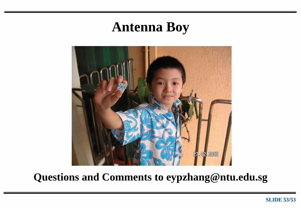
SLIDE 1/53
Antenna-in-Package (AiP) Technology
Y. P. Zhang, FIEEE
Micro Radio Group
Integrated System Research Lab
School of Electrical and Electronic Engineering
Nanyang Technological University (NTU)
Singapore
Forum for Electromagnetic Research Methods and Application Technologies (FERMAT)
by

SLIDE 2/53
Abstract
The antenna-in-package (AiP ) technology combines an antenna (or antennas) with a single-chip radio die into a standard surface mounted
device symbolizing an innovative and important development in the
miniaturization of wireless communications systems in recent years.
The AiP technology is now the mainstream antenna technology and
has been widely adopted by chip makers for 60 GHz radios. The slides
focus on the development of the AiP technology in low-temperature
cofired ceramic (LTCC) process for 60 GHz radios by Y. P. Zhang and
his students and collaborators.
*This use of this work is restricted solely for academic purposes. The author of this work owns the copyright and no reproduction in any form is permitted without written permission by the author.*

SLIDE 3/53
Key Words
Antenna: Discrete antenna, integrat ed antenna, and AiP; Package: Wire-bond package, flip-chip package; Circuit: Discrete circuit,
integrated circuit; Chip: Packaged die, bare die; Process: LTCC,
PCB, and CMOS.

SLIDE 4/53
What is AiP Technology? AiP technology is an antenna solution technology that implements an
antenna or antennas on (or in) an IC package that can carry a highly-
integrated radio or radar transceiver die (or dies).
RF Transceiver Die
Antenna

SLIDE 5/53
Why AiP Technology? As compared with current chip antenna solution, AiP has better system
performance, smaller system PCB area, lower system and assembly
cost, and shorter time to market. Obviously, AiP offers an elegant
antenna solution to single-chip radio or radar transceivers.
Chip Antenna
AiP

SLIDE 6/53
How AiP Technology Evolved? Inspired from the similarity between ceramic patch antenna1 and
hermetic ceramic package2, AiP5-7 evolved from used ceramic package3
through PCB mockup4.

SLIDE 7/53
Who Have Created Knowledge about AiP?

SLIDE 8/53
Who Have Created Knowledge about AiP?
SLIDE 9/53
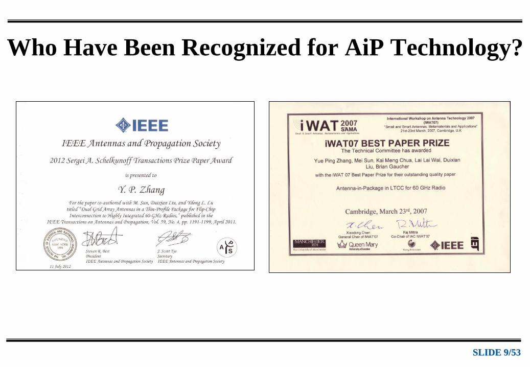
Who Have Been Recognized for AiP Technology?

SLIDE 10/53
Who Else Contributed to AiP Technology?
Incomplete list of early AiP contributors
IMEC CUHK YONSEI PRC
ITRI AMKOR
FRACTUS
Insight SiP
IMST
FRACTUS

SLIDE 11/53
Who Else Contributed to AiP Technology?
NEC IBM
Panasonic
Incomplete list of early AiP contributors

SLIDE 12/53
Infineon
SAMSUNG
STM
IBM
Who Developing AiP Technology Right Now?
Incomplete list of current AiP developers
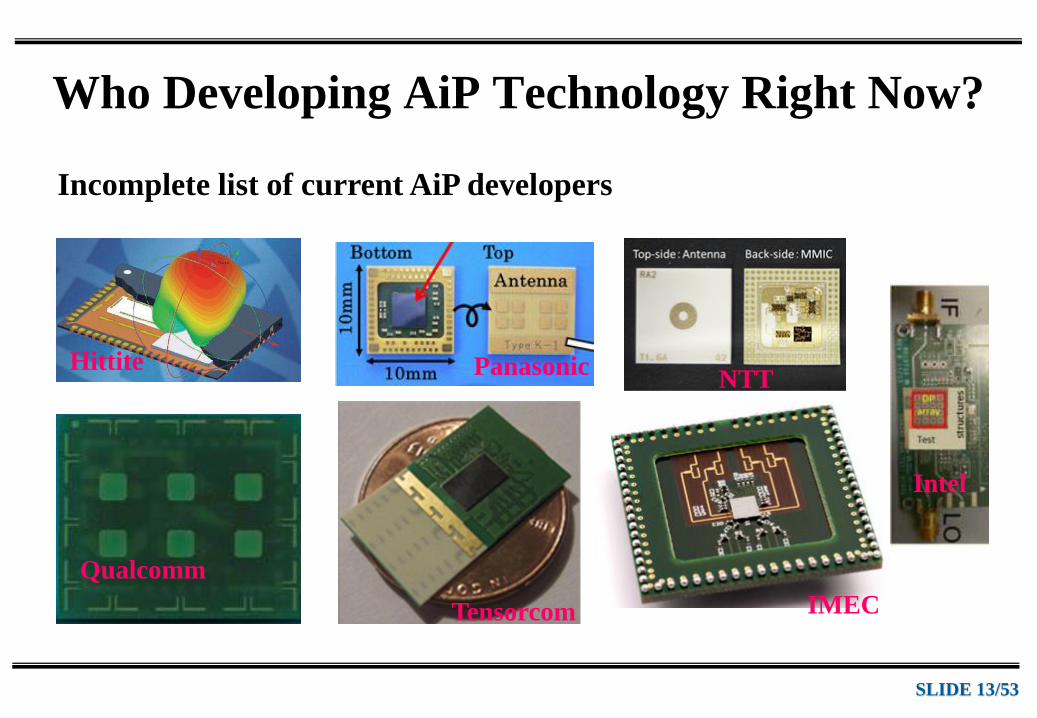
SLIDE 13/53
IMEC
Hittite
Tensorcom
Qualcomm
Who Developing AiP Technology Right Now?
Incomplete list of current AiP developers
Panasonic NTT
Intel

SLIDE 14/53
AiP Technology
AiP for Rx AiP for Tx
10 mm
It is now the mainstream antenna technology for 60 GHz.

SLIDE 15/53
AiP Design
Fig. 4. Design methodology.
Codesign of antenna and package will maximize the AiP performance. Of course,
it would be much better if chip could be also included in the design flow.
Package
Antenna
3D EM
Simulation
HFSS
2D EM
Simulation
IE3D
Design
Released
Provisional
Specification
Can not meet
specification
Meet
specification Meet
specification

SLIDE 16/53
AiP Fabrication
Fig. 5. LTCC Fabrication Facilities (SIMTech).
Low temperature cofired ceramic (LTCC) material and process are suitable for AiP
mass production.

SLIDE 17/53
AiP Measurement
2
212
11
21221
211
1
212
SS
SSSZZ od
Fig. 6. Measurement setup (IBM).
Probe-based measurement setup is needed to measure an AiP and a balun for a
differential signal operation.
(1)
cd
cd
ZZ
ZZRL
10log20 (2)
where Zo = 50 W and Zc = 100 W.
Antenna arm
Wave guide twist
Antenna under test & probe
Motor

SLIDE 18/53
Regulations for 60-GHz Radio
Realized in 1995 that
unlicensed use could be an
appropriate regime for
using such spectrum since
most of the justifications
for radio licensing were
not applicable in these
frequencies. Japan first
issued 60-GHz regulation
for unlicensed utilization
in the 60-GHz band in the
year of 2000.

SLIDE 19/53
WirelessHD
ECMA
IEEE 802.15.3c
WiGig
IEEE 802.11ad
CWPAN
To encompass available but inconsistent unlicensed frequencies, the IEEE 802.15.3c
standard divides nearly 9 GHz of spectrum from 57.24-65.88 GHz into four 2.16-GHz
channels.
Supports data
transmission rates up
to 7 Gbps.
Standards for 60-GHz Radio

SLIDE 20/53
Technology
Interco
nn
ect
Den
sity
Mech
an
ical
Sta
bility
Th
ermal
Co
nd
uctiv
ity
RF
Loss
An
tenn
a
Co
st
Ma
turity
Si-interposer
/Through-Si-Via
LTCC
Laminate
Laminate requires compromise / material development to provide better capability.
Si-interposers/ TSV
– Current efforts
for 3D-integration
don’t address the
needs of 60GHz.
Low temperature
co-fired ceramic
(LTCC) technology
is established for
mm-wave
applications.
Wire bonding possible and flip-chip bonding suitable for 60-GHz die attach.
Package Technology Choices for 60-GHz Radio
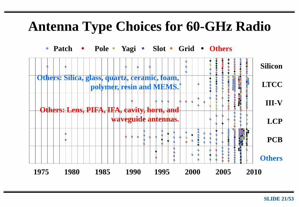
SLIDE 21/53
1975 1980 1985 1990 1995 2000 2005 2010
Silicon
LTCC
III-V
LCP
PCB
Others
Patch Pole Yagi Slot Grid Others
Others: Silica, glass, quartz, ceramic, foam,
polymer, resin and MEMS.
Others: Lens, PIFA, IFA, cavity, horn, and
waveguide antennas.
Antenna Type Choices for 60-GHz Radio

SLIDE 22/53
LTCC Electrical Mechanical Thermal Conductor
εr tanδ MPa GPa ppm/K W/mK
A6 M 5.7 0.0023 170 92 7 2 Au
ACX 7.5 0.01 NA NA 4.7 NA Cu
943 7.4 0.002 230 150 6 4.4 Ag
GL 940 18.7 0.00025 220 188 10.7 3.5 Ag
GL 950 9.4 0.0014 400 173 8.5 4.1 Ag
GL 330 7.5 0.0015 400 178 8.2 4.3 Cu
GL 570 5.6 0.0019 200 128 3.4 2.8 Cu
GL 771 5.2 0.0036 170 74 12.3 3.0 Cu
LTCC Material Properties

SLIDE 23/53
E
L1
L2
J
M
Q J
B
A C
D H G
N
F
K
Inner pattern
via
W/B pads
O
Su
bstra
te edg
e
P
Items Symbol Specification
(Min in mm)
W/B pad width A 0.125
W/B pad width B 0.200
Gap between W/B pads C 0.100
Line width D 0.100
Line to part pad spacing E 0.150
Cavity to part pad spacing F 0.200
Cavity to W/B pad spacing G 0.200
Cavity to cavity spacing H 1.000
Cavity to substrate edge J 1.000
Line to line spacing K 0.100
Cavity to line (surface) L1 0.200
Cavity to line (inner) L2 0.200
Via (d) pitch or to part edge M 2d
W/B pad to line N 0.100
Conner of cavity O 0.150
W/B pad to via edge P 0.200
Via edge to cavity edge Q 0.250
LTCC Design Rules

SLIDE 24/53
≥ 0.2 mm ≥ 0.15 mm
≥ 0.4 mm
= 0.25 mm = 0.55 mm
= 0.35 mm
= 0.38 mm
Au W/B pad = 0.25 mm × 0.25 mm
Au extension = 0.15 mm × 0.35 mm
Au catch pad diameter 0.25 mm
W/B pad offset = 0.25 mm
LTCC Design Rules

SLIDE 25/53
Finished part dimensional tolerance is generally ± 0.7 % of part size but not less than
± 100μm for green cut parts.
The shrinkage tolerance of circuit features in x and y direction is typically less than
± 0.1 % (production ± 0.2% typically).
The minimum recommended substrate thickness is 500 μm. Layer thickness
tolerance is ± 7 % (typically < ± 2% within manufacturing lot).
The via hole punching to the tape sheet can be made typically to 10 μm accuracy
in production.
The layer-to-layer alignment accuracy for via and conductor is typically 10~20 μm.
The screen printed conductor alignment error is typically 5~10 μm.
The line width tolerance is typically 5%.
Dielectric constant of 5.9 ± 0.2, loss tangent of 0.002 ± 0.02% , and conductivity of
2.5 ×10⁷ S/m for A6M at 60 GHz.
LTCC Tolerances
www.ltcc.de

SLIDE 26/53
Conductor roughness
• Increase in conductor loss more than 2 times (experimentally demonstrated).
• Affects effective permittivity.
• Affects phase constant especially in thinner substrates
Ceramic roughness
• Affects thickness (so impedance).
• Affects effective permittivity.
LTCC Roughness
www.ltcc.de

SLIDE 27/53
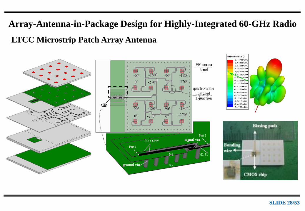
Array-Antenna-in-Package Design for Highly-Integrated 60-GHz Radio
Microstrip Patch Array Antenna
Major advantages: Low profile, conformable to planar and non-planar surfaces, easy
to design, simple to manufacture, compatible with both single-ended and differential
silicon radio.
Major disadvantages: Low efficiency, high Q, poor polarization purity, spurious feed
radiation and very narrow impedance bandwidth.
SLIDE 28/53
Array-Antenna-in-Package Design for Highly-Integrated 60-GHz Radio
LTCC Microstrip Patch Array Antenna

SLIDE 29/53
Array-Antenna-in-Package Design for Highly-Integrated 60-GHz Radio
LTCC Microstrip Patch Array Antenna
SLIDE 30/53
Array-Antenna-in-Package Design for Highly-Integrated 60-GHz Radio
Microstrip Grid Array Antenna
It was invented by Kraus in 1964, revived by Conti, et al in 1981, and studied by
Nakano, et al at lower microwave frequencies.
Major structural advantages: Low profile, conformable to planar and non-planar
surfaces, easy to design, simple to manufacture, simple feeding network, compatible
with both single-ended and differential silicon radio.
Major operational advantages: High efficiency, high gain, good polarization purity,
wide impedance and gain bandwidth, can be travelling-wave and able to beam steering
by frequency shift, can be resonant with boresight beam radiation.
SLIDE 31/53
Array-Antenna-in-Package Design for Highly-Integrated 60-GHz Radio
Microstrip Grid Array Antenna Design Guidelines and Examples
Choice of substrate: A thick substrate means using a low dielectric
constant to limit the generation of surface waves.
Number of loops: Given the specified gain G, the number of loops can
be estimated by 2×10(G-Gd)/10 where Gd is the gain of microstrip half-
wave dipole.
Loop short side design: A short side is a radiating element. The
length is required to be λg/2 for resonance. The width sets the
radiation resistance, which is governed by the desired amplitude taper
on the array.
Loop long side design: A long sideis a transmission line. The length is
required to be λg for resonance. The width sets the characteristic
impedance, which should match the short side impedance.

SLIDE 32/53
Array-Antenna-in-Package Design for Highly-Integrated 60-GHz Radio
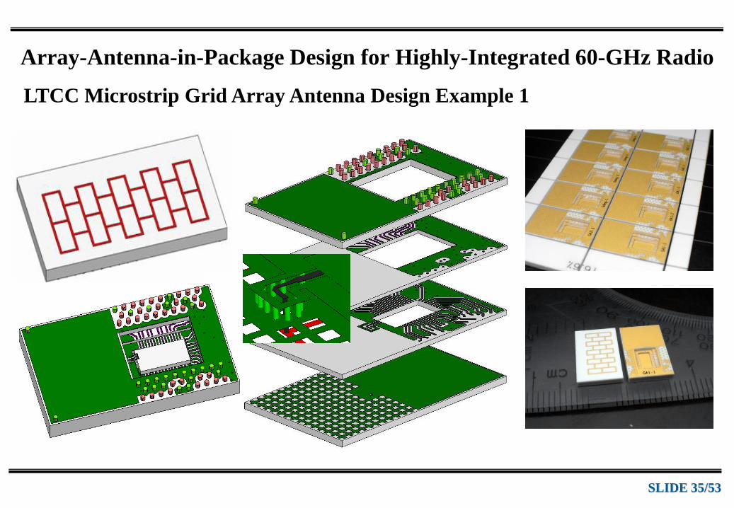
LTCC Microstrip Grid Array Antenna Design Example 1
xv
yv
l
w
dv
da
Single Feed Design
Number of meshes 14
Mesh dimensions l = 2.5 mm ≈ λg, w = 1.365 mm ≈ λg/2
Substrate dimensions 13.5mm×8mm×0.375 mm
Line width and thickness 0.15mm and 0.01 mm
Excitation location xv = 7.3 mm, yv = 3.98 mm
Feeding dimensions dv= 0.1 mm, da = 0.3mm
Specifications @ 60 GHz in Ferro LTCC A6M
Bandwidth = 7 GHz, efficiency > 80%, and maximum
gain = 15 dBi

SLIDE 33/53
Array-Antenna-in-Package Design for Highly-Integrated 60-GHz Radio
LTCC Microstrip Grid Array Antenna Design Example 1
Frequency (GHz)
51 53 55 57 59 61 63 65 67 69
mag
(S11
) (d
B)
-25
-20
-15
-10
-5
0
Frequency (GHz)
50 52 54 56 58 60 62 64 66 68 70
Peak
Rea
lized
Gai
n (d
Bi)
0
5
10
15
20
Simulations show that large impedance bandwidth of 13 GHz (21.4% @ 61.5 GHz),
maximum gain of 15 dBi, and 3-dB gain bandwidth of 10 GHz are achieved.

SLIDE 34/53
Array-Antenna-in-Package Design for Highly-Integrated 60-GHz Radio
LTCC Microstrip Grid Array Antenna Design Example 1
-40dB
-30dB
-20dB
-10dB
0dB0
30
60
90
120
150
180
210
240
270
300
330
Co
Cross
= 0
z
x-40dB
-30dB
-20dB
-10dB
0dB0
30
60
90
120
150
180
210
240
270
300
330
Co
Cross
= 0
z
y
y
z
x
Simulations show that desirable patterns with low side lobe and week cross-polarization
radiation are achieved.
SLIDE 35/53
Array-Antenna-in-Package Design for Highly-Integrated 60-GHz Radio
LTCC Microstrip Grid Array Antenna Design Example 1

SLIDE 36/53
Array-Antenna-in-Package Design for Highly-Integrated 60-GHz Radio
LTCC Microstrip Grid Array Antenna Design Example 1
An excellent matching to a 50-Ω source achieved from 56.3-65 GHz. The measured
and calculated peak gain values are both 14.5 dBi with estimated efficiency better
than 95% at 60-GHz. No de-embedding was made between the post-layout
simulation and measurement.
Frequency (GHz)55 56 57 58 59 60 61 62 63 64 65
mag
(S1
1)
(dB
)
-35
-30
-25
-20
-15
-10
-5
0Measured
Simulated
Frequency (GHz)55 56 57 58 59 60 61 62 63 64 65
Pea
k g
ain
(d
Bi)
-5
0
5
10
15
20
25
Eff
icie
ncy
.6
.7
.8
.9
1.0
Measured gain
Simulated gain
Simulated efficiency

SLIDE 37/53
Array-Antenna-in-Package Design for Highly-Integrated 60-GHz Radio
-40dB
-30dB
-20dB
-10dB
0dB0
30
60
90
120
150
180
210
240
270
300
330
Measured, Co
Measured, Cross
Simulated, Co
Simulated, Cross
= 0
z
x-40dB
-30dB
-20dB
-10dB
0dB0
30
60
90
120
150
180
210
240
270
300
330
Measured, Co
Measured, Cross
Simulated, Co
Simulated, Cross
= 0
z
y
60 GHz
LTCC Microstrip Grid Array Antenna Design Example 1

SLIDE 38/53
Array-Antenna-in-Package Design for Highly-Integrated 60-GHz Radio
LTCC Microstrip Grid Array Antenna Design Example 2
xv1
yv
l
w
dv
da
Dual Feed Design
Number of meshes 14
Mesh dimensions l = 2.5 mm ≈ λg, w = 1.365 mm ≈ λg/2
Substrate dimensions 13.5mm×8mm×0.375 mm
Line width and thickness 0.15mm and 0.01 mm
Excitation location xv1 = 4.57 mm, xv2 = 3.5 mm,
yv = 3.98 mm
Feeding dimensions dv= 0.1 mm, da = 0.3mm
Specifications @ 60 GHz in Ferro LTCC A6M
Bandwidth = 7 GHz, efficiency > 80%, and maximum
gain = 15 dBi
xv2
yv

SLIDE 39/53
Array-Antenna-in-Package Design for Highly-Integrated 60-GHz Radio
LTCC Microstrip Grid Array Antenna Design Example 2
Simulations show that large impedance bandwidth of 10 GHz (16.3% @ 61.5 GHz)
and maximum gain of 14 dBi for single-ended excitation and of 8 GHz (13% @ 61.5
GHz) maximum gain of 16 dBi for differential excitation are achieved, respectively.
Frequency (GHz)50 52 54 56 58 60 62 64 66 68 70
Ret
urn
lo
ss (
dB
)
0
5
10
15
20
25
30
35
diff
single
Frequency (GHz)50 52 54 56 58 60 62 64 66 68 70
Pea
k r
eali
zed
gai
n
(dB
i)
0
5
10
15
20
diff
single

SLIDE 40/53
Array-Antenna-in-Package Design for Highly-Integrated 60-GHz Radio
LTCC Microstrip Grid Array Antenna Design Example 2
Simulations show that differential excitation has narrower beamwidth in the E plane
and similar beamwidth in the H plane than those of single-ended excitation.
-40dB
-30dB
-20dB
-10dB
0dB
0
30
60
90
120
150
180
210
240
270
300
330
co, diff
cross, diff
co, single
cross, single
= 0
z
x-40dB
-30dB
-20dB
-10dB
0dB
0
30
60
90
120
150
180
210
240
270
300
330
co, diff
cross, diff
co, single
cross, single
= 0
z
x
y
z
x

SLIDE 41/53
Array-Antenna-in-Package Design for Highly-Integrated 60-GHz Radio
LTCC Microstrip Grid Array Antenna Design Example 2
Solder balls
PCB cavity
M1 M2 M3 M4
60-GHz radio diePCB board
Vd- Vd+ Vs

SLIDE 42/53
Array-Antenna-in-Package Design for Highly-Integrated 60-GHz Radio
LTCC Microstrip Grid Array Antenna Design Example 2
Frequency (GHz)55 56 57 58 59 60 61 62 63 64 65
Ret
urn
lo
ss
(dB
)
0
5
10
15
20
25
30
35
Measured
Simulated
Frequency (GHz)55 56 57 58 59 60 61 62 63 64 65
Pea
k r
eali
zed
gai
n
(dB
i)
-5
0
5
10
15
20
25
Eff
icie
ncy
.6
.7
.8
.9
1.0
Measured peak realized gain
Simulated peak realized gain
Simulated efficiency
An excellent matching to a 50-Ω source achieved from 56.3-63.2 GHz. The
measured and calculated peak realized gain values agree well with estimated
efficiency better than 95% at 60-GHz. No de-embedding was made between the
post-layout simulation and measurement.

SLIDE 43/53
Array-Antenna-in-Package Design for Highly-Integrated 60-GHz Radio
LTCC Microstrip Grid Array Antenna Design Example 2
-40dB
-30dB
-20dB
-10dB
0dB0
30
60
90
120
150
180
210
240
270
300
330= 0
z
x-40dB
-30dB
-20dB
-10dB
0dB0
30
60
90
120
150
180
210
240
270
300
330= 0
z
x
60 GHz
SLIDE 44/53
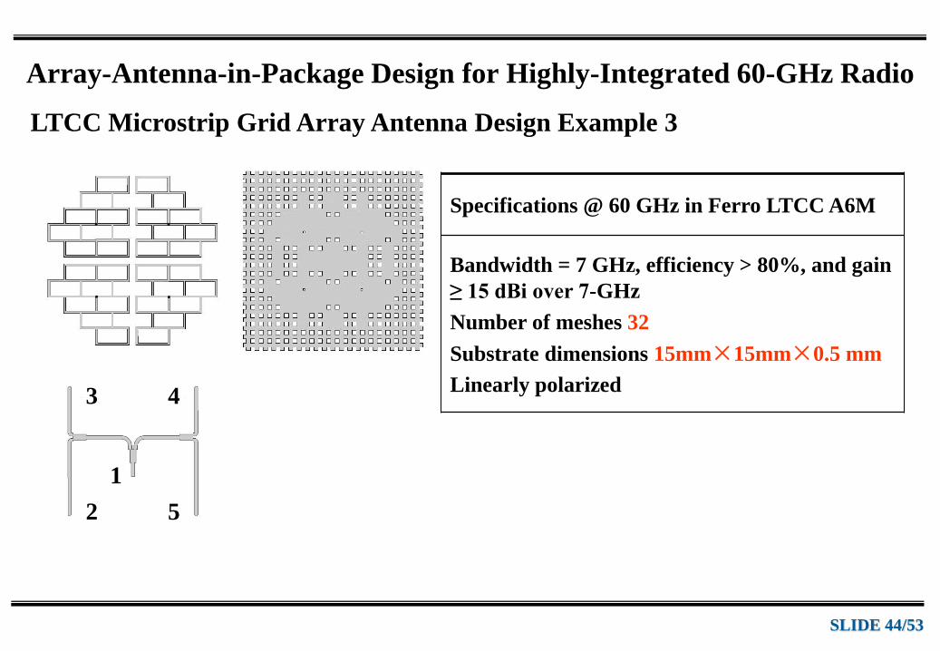
Array-Antenna-in-Package Design for Highly-Integrated 60-GHz Radio
LTCC Microstrip Grid Array Antenna Design Example 3
1
3 4
5 2
Specifications @ 60 GHz in Ferro LTCC A6M
Bandwidth = 7 GHz, efficiency > 80%, and gain
≥ 15 dBi over 7-GHz
Number of meshes 32
Substrate dimensions 15mm×15mm×0.5 mm
Linearly polarized

SLIDE 45/53
Array-Antenna-in-Package Design for Highly-Integrated 60-GHz Radio
LTCC Microstrip Grid Array Antenna Design Example 3

SLIDE 46/53
Array-Antenna-in-Package Design for Highly-Integrated 60-GHz Radio
LTCC Microstrip Grid Array Antenna Design Example 3
50 52 54 56 58 60 62 64 66 68 70-55
-50
-45
-40
-35
-30
-25
-20
-15
-10
-5
0
|S1
1| (d
B)
Frequency (GHz)
Pre simulation without signal traces
Measured without signal traces
Measured with signal traces
Post simulation without signal traces
50 52 54 56 58 60 62 64 66 68 70-10
-8
-6
-4
-2
0
2
4
6
8
10
12
14
16
18
Pea
k r
eali
zed
ga
in (
dB
i)
Frequency (GHz)
Pre simulation without signal traces
Measured without signal traces
Measured with signal traces
Post simulation wihout signal traces

SLIDE 47/53
Array-Antenna-in-Package Design for Highly-Integrated 60-GHz Radio
LTCC Microstrip Grid Array Antenna Design Example 3 60 GHz
(a) (b)60 GHz

SLIDE 48/53
Concluding Remarks
The AiP technology originated from Zhang’s work has emerged as the most
elegant antenna solution to modern radio systems.
The AiP technology has been demonstrated for WLAN, UWB, and millimeter-
wave (60 GHz) radios, respectively.
The AiP technology combines an antenna (or antennas) with a single-chip radio
die into a standard surface mounted device symbolizing an innovative and
important development in the miniaturization of wireless communications
systems in recent years.

SLIDE 49/53
Acknowledgement
Zhang would like to acknowledge the contribution from his former students:
Mr. Xue Yang, Mr. Lin Wei, Dr. Wang Junjun, Dr. Sun Mei, Dr. Zhang Bing and
from his collaborators: Mr. Chua Kai Meng, Ms. Wai Lai Lai, and Dr. Albert Lu
Chee Wai from Singapore Institute of Manufacturing Technology, Dr. Liu Duixian
and Mr. Brain P. Gaucher from IBM T. J. Watson Research Center, USA , and
Prof. C. Luxey, Dr D. Titz, and Dr. F. Ferrero from Université Nice Sophia-
Antipolis , France in the development of AiP technology.
SLIDE 50/53
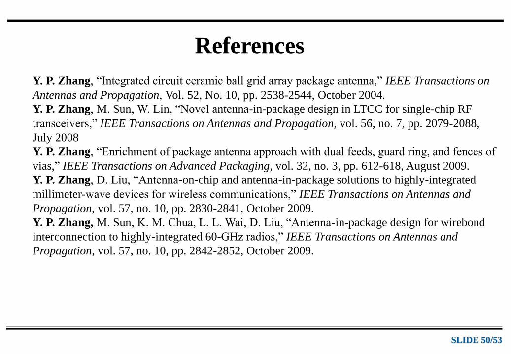
References
Y. P. Zhang, “Integrated circuit ceramic ball grid array package antenna,” IEEE Transactions on
Antennas and Propagation, Vol. 52, No. 10, pp. 2538-2544, October 2004.
Y. P. Zhang, M. Sun, W. Lin, “Novel antenna-in-package design in LTCC for single-chip RF
transceivers,” IEEE Transactions on Antennas and Propagation, vol. 56, no. 7, pp. 2079-2088,
July 2008
Y. P. Zhang, “Enrichment of package antenna approach with dual feeds, guard ring, and fences of
vias,” IEEE Transactions on Advanced Packaging, vol. 32, no. 3, pp. 612-618, August 2009.
Y. P. Zhang, D. Liu, “Antenna-on-chip and antenna-in-package solutions to highly-integrated
millimeter-wave devices for wireless communications,” IEEE Transactions on Antennas and
Propagation, vol. 57, no. 10, pp. 2830-2841, October 2009.
Y. P. Zhang, M. Sun, K. M. Chua, L. L. Wai, D. Liu, “Antenna-in-package design for wirebond
interconnection to highly-integrated 60-GHz radios,” IEEE Transactions on Antennas and
Propagation, vol. 57, no. 10, pp. 2842-2852, October 2009.
SLIDE 51/53
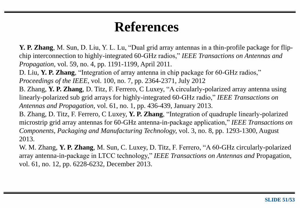
References
Y. P. Zhang, M. Sun, D. Liu, Y. L. Lu, “Dual grid array antennas in a thin-profile package for flip-
chip interconnection to highly-integrated 60-GHz radios,” IEEE Transactions on Antennas and
Propagation, vol. 59, no. 4, pp. 1191-1199, April 2011.
D. Liu, Y. P. Zhang, “Integration of array antenna in chip package for 60-GHz radios,”
Proceedings of the IEEE, vol. 100, no. 7, pp. 2364-2371, July 2012
B. Zhang, Y. P. Zhang, D. Titz, F. Ferrero, C Luxey, “A circularly-polarized array antenna using
linearly-polarized sub grid arrays for highly-integrated 60-GHz radio,” IEEE Transactions on
Antennas and Propagation, vol. 61, no. 1, pp. 436-439, January 2013.
B. Zhang, D. Titz, F. Ferrero, C Luxey, Y. P. Zhang, “Integration of quadruple linearly-polarized
microstrip grid array antennas for 60-GHz antenna-in-package application,” IEEE Transactions on
Components, Packaging and Manufacturing Technology, vol. 3, no. 8, pp. 1293-1300, August
2013.
W. M. Zhang, Y. P. Zhang, M. Sun, C. Luxey, D. Titz, F. Ferrero, “A 60-GHz circularly-polarized
array antenna-in-package in LTCC technology,” IEEE Transactions on Antennas and Propagation,
vol. 61, no. 12, pp. 6228-6232, December 2013.

SLIDE 52/53
Biography
Y. P. ZHANG is a Professor of Electronic Engineering with the
School of Electrical and Electronic Engineering at Nanyang
Technological University, Singapore. He serves as an Associate
Editor of the IEEE Transactions on Antennas and Propagation. He
received the S. A. Schelkunoff Transactions Prize Paper Award of
the IEEE Antennas and Propagation Society (2012). He was the
Chair, leading the Singapore Chapter to win the Best Chapter Award
of the IEEE Antennas and Propagation Society (2013). He was the
Advisor, guiding the Singapore Chapter to win the Outstanding
Chapter Award of the IEEE Microwave Theory and Technique
Society
(2014). He was elevated as a Fellow of IEEE in 2009 for his
contributions in subsurface radio and integrated antenna.