appendix a: hardware description language (hdl)1 · appendix a: hardware description language ... a...
TRANSCRIPT
Appendix A: HDL 1
Appendix A: Hardware Description Language (HDL)1
Intelligence is the faculty of making artificial objects, especially tools to make tools.
Henry Bergson, (1859-1941)
A Hardware Description Language (HDL) is a formalism used to define and test chips: objects whose interfaces consist of input and output pins that carry Boolean signals, and whose bodies are composed of inter-connected collections of other, lower level, chips. This appendix describes a typical HDL, as understood by the hardware simulator supplied with the book. Chapter 1 provides essential background to this appendix, and thus it is recommended to read it first. How to use this appendix: This is a technical document, and thus there is no need to read it from beginning to end. Instead, it is recommended to focus on selected sections, as needed. Also, HDL is an intuitive and self-explanatory language, and the best way to learn it is to play with some HDL programs in the hardware simulator. Therefore, we recommend to start experimenting with HDL programs as soon as you can, beginning with the following example. 1. Example The following HDL program specifies a chip that accepts two 4-bit numbers and outputs whether they are equal or not. The chip logic uses Xor gates to compare the 4 bit-pairs, and then outputs true if all the comparisons are “equal”.
/** Returns 1 if the two inputs are equal and 0 otherwise. */ CHIP EQ4 { IN a[4],b[4]; // 4-bit busses OUT out; // true iff a=b PARTS: Xor(a=a[0],b=b[0],out=c0); Xor(a=a[1],b=b[1],out=c1); Xor(a=a[2],b=b[2],out=c2); Xor(a=a[3],b=b[3],out=c3); Or(a=c0,b=c1,out=c01); Or(a=c01,b=c2,out=c012); Or(a=c012,b=c3,out=neq); Not(in=neq,out=out); }
Each internal part Xxx invoked by an HDL program is in itself a stand-alone chip defined in a separate Xxx.hdl program like the one listed above. Thus the chip designer who wrote the above program assumed the existence of three other chips: Xor.hdl, Or.hdl, and Not.hdl.
1 From The Elements of Computing Systems, Nisan & Schocken, MIT Press, forthcoming in 2003, www.idc.ac.il/csd
Appendix A: HDL 2 Importantly, though, the chip designer need not worry about how these chips are implemented. The internal parts are always viewed as black boxes, allowing the designer to focus only on their proper arrangement in the current chip architecture. Thanks to this modularity, all HDL programs, including those that describe high-level chips, can be kept short and readable. For example, a complex chip like RAM32K can be implemented using a few internal parts, each described in a single HDL line. When fully evaluated by the hardware simulator all the way down the recursive chip hierarchy, these internal parts are expanded into many thousands of inter-connected elementary logic gates. Yet the chip designer need not be concerned by this complexity, and can focus instead only on the chip’s topmost architecture. Comment: the EQ4.hdl program is not supplied with the book. If you want to experiment with it, you have to create the EQ4.hdl text file and load it into the hardware simulator. 2. Conventions File Extension: Each chip is defined in a separate text file. A chip whose name is Xxx is defined in file Xxx.hdl. Chip structure: A chip definition consists of a header and a body. The header provides a full specification of the chip interface, while the body describes the chip implementation. The header acts as the chip’s API, or public documentation. The body should not interest people who use the chip as internal part in other chip definitions. Syntax conventions: HDL is case-sensitive. By convention, HDL keywords are written in upper-case letters. Identifiers naming: Names of chips and pins may be any sequence of letters and digits not starting with a digit. By convention, chip and pin names start with a capital letter and a lower-case letter, respectively. For readability, upper-case letters can be used in the middle of identifier names. White space: Space characters, newline characters, and comments are ignored. Comments: The following three comment formats are supported:
// comment to end of line /* comment until closing */ /** API documentation comment */
3. Loading Chips into the Simulator HDL programs (chip descriptions) are loaded into the simulator environment in three different ways. First, the user can open an HDL file interactively, via a "load file" menu or GUI icon. Second, a test script (discussed below) can include a "load Xxx.hdl" command, which has the same effect. Finally, whenever an HDL program is loaded and parsed (e.g. EQ4.hdl), every chip name Yyy listed in it as internal part (e.g. Xor) causes the simulator to load the respective
Appendix A: HDL 3 Yyy.hdl file (e.g. Xor.hdl), all the way down the recursive chip hierarchy. In every one of these cases, the simulator goes through the following logic:
if <chip name>.hdl exists in the current directory then load it (and all its descendents) into the simulator else if <chip name>.hdl exists in the simulator’s BuiltIn chips directory then load it (and all its descendents) into the simulator else issue an error message.
The simulator’s BuiltIn directory contains executable versions of all the chips specified in the book, except for the highest-level chips (CPU, Memory, and Computer). Hence, one may construct and test a chip before all, or even any, of its lower-level chip parts have been implemented: the simulator will automatically invoke their built-in versions instead. Alternatively, if a lower-level chip Xxx has been implemented by the user in HDL, the user can still force the simulator to use its built-in version instead, by simply moving the Xxx.hdl file out from the current directory. Finally, in some cases the user (rather than the simulator) may want to load a built-in chip directly, e.g. for experimentation. To do so, navigate to the BuiltIn directory – a standard part of the hardware simulator environment -- and select the desired chip from there. 4. Chip Header (Interface) The header of an HDL program has the following format:
CHIP <chip name> { IN <input pin name>, <input pin name>, ... ; OUT <output pin name>, <output pin name>, ... ; // Here Comes the Body }
CHIP declaration: The CHIP keyword is followed by the chip name. The rest of the HDL code appears between curly brackets.
Input pins: The IN keyword is followed by a comma-separated list of the names of the chip input pins. The list is terminated with a semi-colon.
Output pins: The OUT keyword is followed by a comma-separated list of the names of the chip output pins. The list is terminated with a semi-colon.
Input and output pins are assumed by default to be single-bit wide. A multi-bit bus can be declared using the notation <pin name>[w]. (e.g. “a[4]” in EQ4.hdl). This specifies that the pin is a bus of width w. The individual bits in a bus are indexed 0 ... w-1, from right to left (i.e. index 0 refers to the least significant bit).
Appendix A: HDL 4 5. Chip Body (Implementation)
Parts A chip typically consists of several lower-level chips, connected to each other and to the chip input/output pins in a certain topology that forms the chip logic. This logic, designed by the HDL programmer to deliver the chip’s desired functionality, is described in the chip body using the following format:
PARTS: <internal chip part>; <internal chip part>; . . . <internal chip part>;
Each one of these statements describes one internal chip with all its connections, using the following syntax:
<chip name>(<connection>, ... , <connection>); Throughout this document, the presently defined chip is called chip, and the lower level chips listed in the PARTS section are called parts.
Pins and Connections The syntax of a connection specification is:
<part's pin name> = <chip's pin name>
Connections describe how a part is connected to the overall chip architecture: each connection describes how one pin of the part is connected to another pin in the chip definition. In the simplest case, one may connect the part’s pin to an input or output pin of the chip. In other cases, we have to connect the part’s pin to another pin of another part. This is done by defining an internal pin (a chip level object), and connecting the pins of the two parts to it. Thus, the definition of an internal pin is essentially the same as creating and naming a wire that connects an output pin of one chip to the input pin of another. Internal pins: In order to connect an output pin of Part1 to the input pins of other parts, the HDL programmer can create and use an internal pin, say v, as follows:
Part1(...,out=v); // out of Part1 is piped into v Part2(in=v,...); // v is piped into in of Part2 Part3(a=v, b=v,...); // v is piped into a and b of Part 3
An internal pin (like v above) acts like a pipe that receives a value from one part and feeds it into one or more other parts. Internal pins are created as needed when they are specified the first time in the HDL program, and require no other definition. Each internal pin has fan-in 1 and unlimited fan-out. In other words, an internal pin can be fed from a single source only, yet it can feed (through multiple connections) many other parts. In the above example, the internal pin v simultaneously feeds both Part2 (through in) and Part3 (though a and b).
Appendix A: HDL 5 Input pins: Each input pin of a part may be fed by one of the following sources:
• An input pin of the chip;
• An internal pin;
• One of the constants true and false, representing 1 and 0, respectively. Each input pin has fan-in 1, meaning that it can be fed by one source only. Thus Part(a=v,b=v,...) is a valid statement (assuming that both a and b are input pins of the part), whereas Part(a=v,a=u,...) is not. Output pins: Each output pin of a part may feed one of the following destinations:
• An output pin of the chip;
• An internal pin.
Buses Each pin used in a connection -- whether input, output, or internal -- may be a multi-bit bus. The widths (number of bits) of input and output pins are defined in the chip header. The widths of internal pins are deduced implicitly by the simulator, as explained below. In order to connect individual elements of a multi-bit bus input or output pin, the pin name (say x) may be sub-scripted using the syntax x[n..m]=v, where v is an internal pin. This means that only the bits indexed n to m (inclusive) of pin x are connected to the specified internal pin. An internal pin (like v above) may not be subscripted, and its width is deduced implicitly from the width of the bus pin to which it is connected the first time it is mentioned in the HDL program. The constants true and false may also be used as buses, in which case the required width is deduced implicitly from the context of the connection. Example: Consider the following chip:
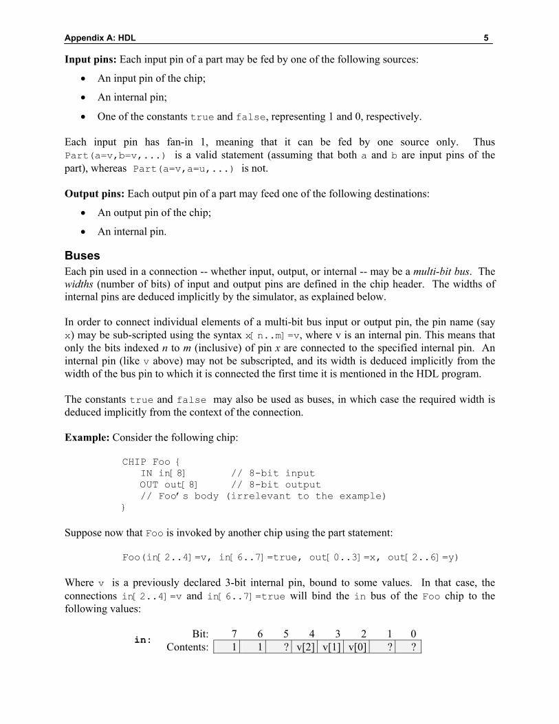
CHIP Foo { IN in[8] // 8-bit input OUT out[8] // 8-bit output // Foo’s body (irrelevant to the example) }
Suppose now that Foo is invoked by another chip using the part statement:
Foo(in[2..4]=v, in[6..7]=true, out[0..3]=x, out[2..6]=y) Where v is a previously declared 3-bit internal pin, bound to some values. In that case, the connections in[2..4]=v and in[6..7]=true will bind the in bus of the Foo chip to the following values:
Bit: 7 6 5 4 3 2 1 0 in: Contents: 1 1 ? v[2] v[1] v[0] ? ?
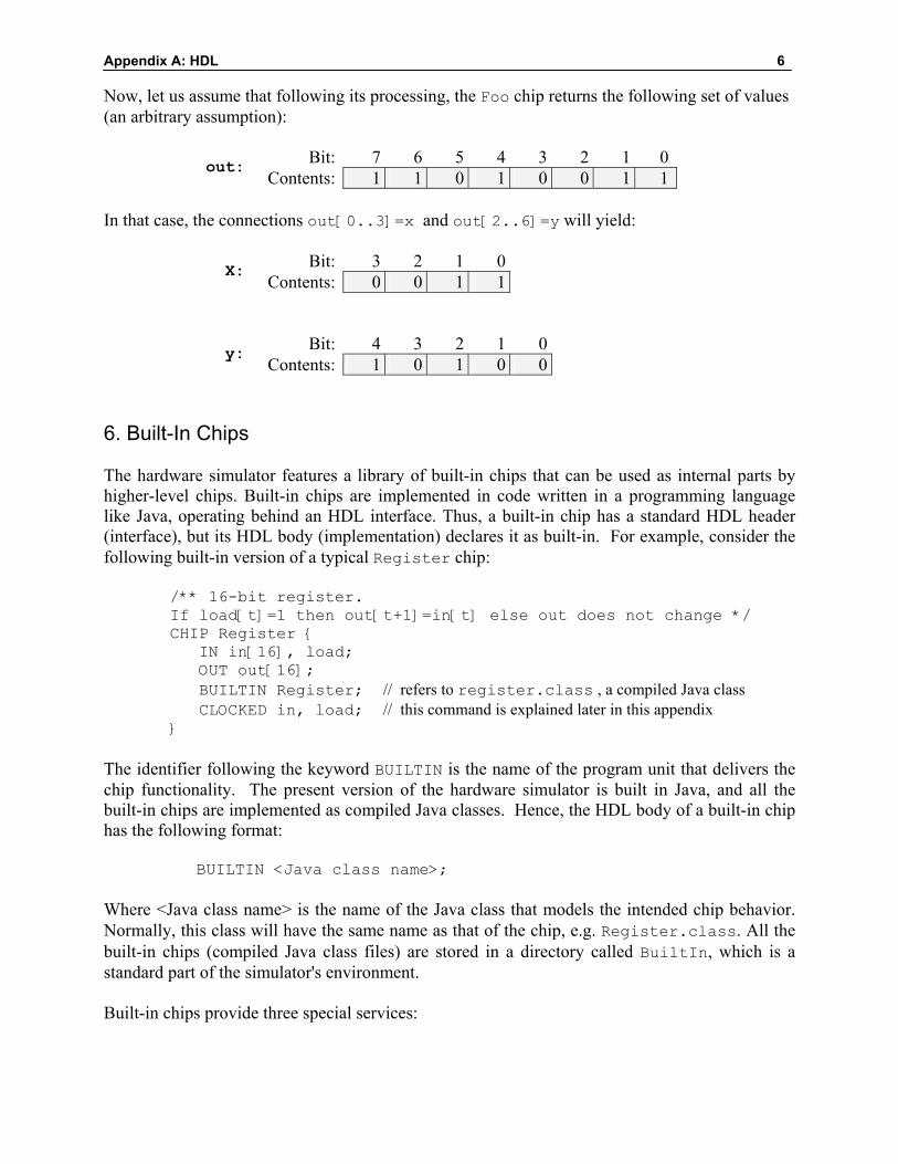
Appendix A: HDL 6 Now, let us assume that following its processing, the Foo chip returns the following set of values (an arbitrary assumption):
Bit: 7 6 5 4 3 2 1 0 out: Contents: 1 1 0 1 0 0 1 1
In that case, the connections out[0..3]=x and out[2..6]=y will yield:
Bit: 3 2 1 0X: Contents: 0 0 1 1
Bit: 4 3 2 1 0y: Contents: 1 0 1 0 0
6. Built-In Chips The hardware simulator features a library of built-in chips that can be used as internal parts by higher-level chips. Built-in chips are implemented in code written in a programming language like Java, operating behind an HDL interface. Thus, a built-in chip has a standard HDL header (interface), but its HDL body (implementation) declares it as built-in. For example, consider the following built-in version of a typical Register chip:
/** 16-bit register. If load[t]=1 then out[t+1]=in[t] else out does not change */ CHIP Register { IN in[16], load; OUT out[16]; BUILTIN Register; // refers to register.class , a compiled Java class CLOCKED in, load; // this command is explained later in this appendix }
The identifier following the keyword BUILTIN is the name of the program unit that delivers the chip functionality. The present version of the hardware simulator is built in Java, and all the built-in chips are implemented as compiled Java classes. Hence, the HDL body of a built-in chip has the following format:
BUILTIN <Java class name>; Where <Java class name> is the name of the Java class that models the intended chip behavior. Normally, this class will have the same name as that of the chip, e.g. Register.class. All the built-in chips (compiled Java class files) are stored in a directory called BuiltIn, which is a standard part of the simulator's environment. Built-in chips provide three special services:
Appendix A: HDL 7 Foundation: Some chips are the atoms from which all other chips are built. In particular,
we use the Nand gate and the D-Flip-Flop gate as the building blocks of all combinational and sequential chips, respectively. Thus the hardware simulator features built-in versions of Nand.hdl and DFF.hdl.
Certification & Efficiency: In order to modularize the development and testing of hardware construction projects, the chips that participate in the project can be made available in built-in versions. Thus one may construct a chip before constructing its lower-level parts – the simulator will automatically invoke their built-in versions. Additionally, it makes sense to use built-in versions even for chips that were already constructed, since the former are typically much faster and more space-efficient than the latter (simulation-wise). For example, consider a RAM4K chip. When you write and debug the file RAM4K.hdl, the simulator creates a memory-resident data structure consisting of thousands of lower-level chips, all the way down to the D-Flip-Flop gates at the bottom of the recursive chip hierarchy. Although this top-down drilling must be done when you develop and test the RAM4K chip, there is no need to repeat it each time the chip is used as part in higher-level chips, e.g. RAM16K. Best practice tip: To boost performance and minimize errors, always use the supplied built-in versions of chips whenever they are available.
Visualization: Some high-level chips, e.g. memory units, are easier to understand and debug if their operation can be inspected visually. To facilitate this service, selected built-in chips can be endowed with GUI side effects. This GUI is displayed whenever the chip is loaded into the simulator or invoked as a lower-level part by the loaded chip. Except for these visual side effects, GUI-empowered chips behave, and can be used, just like any other chip. Section 8 contains more details about GUI-empowered chips.
7. Sequential Chips Computer chips are either combinational or sequential (also called clocked). The operation of combinational chips is instantaneous. Thus, when a user or a test script changes the values of one or more of the input pins of a combinational chip and presses the “eval” button, the simulator responds by immediately setting the chip output pins to a new set of values, as computed by the chip logic. In contrast, the operation of sequential chips is clock-regulated. In particular, when the inputs of a sequential chip change, the outputs of the chip may change to new values only at the beginning of the next time unit, as effected by the simulated clock. In fact, sequential chips may change their output values when the time changes even if none of their inputs changed. In contrast, combinational chips never change their values just because of the progression of time.
The Clock The simulator models the progression of time by a built-in device, called clock, which is controlled by “Tick” and “Tock” operations. These operations generate a series of time units, each consisting of two phases: a “Tick” ends the first phase of a time unit and starts its second phase, and a “Tock” moves to the first phase of the next time unit. The real time that elapsed during this period is irrelevant for simulation purposes, since we have full control over the clock. In other words, either the simulator’s user or a test script can issue Ticks and Tocks at will, causing the clock to generates a series of simulated time units.
Appendix A: HDL 8 The two-phased time units regulate the operations of all the sequential chip parts in the simulated chip architecture, as follows. During the first phase of the time unit (Tick), the inputs of each sequential chip in the architecture are read and affect the chip’s internal state, according to the chip logic. During the second phase of the time unit (Tock), the outputs of the chip are set to the new values. Hence, if we look at a sequential chip “from the outside,” we see that its output pins stabilize to new values only at “Tocks” – between consecutive time units. There are two ways to control the simulated clock: manual and script-based. First, the simulator's GUI features a clock-shaped button called “TickTock”. A “Tick” (one click on this button) ends the first phase of the clock cycle, and a “Tock” (subsequent click) ends the second phase of the cycle, bringing on the first phase of the next cycle, and so on. Alternatively, one can run the clock from a test script, e.g. using the command repeat n {tick,tock,output;}. This script command instructs the simulator to advance the clock n time units, and to print some values in the process. Test scripts and commands like repeat and output are described in detail in appendix B.
Clocked Chips and Pins A built-in chip can declare its dependence on the clock explicitly, using the statement:
CLOCKED <pin>, <pin>, ..., <pin>;
Where each pin is either an input pin or an output pin, as declared in the chip header. The inclusion of an input pin x in the CLOCKED list instructs the simulator that changes to x should not effect any of the chip’s output pins until the beginning of the next time unit. The inclusion of an output pin x in the CLOCKED list instructs the simulator that changes in any of the chip’s input pins should not effect x until the beginning of the next time unit. Note that it is quite possible that only some of the input or output pins of a chip are declared as clocked. In that case, changes in the non-clocked input pins may affect the non-clocked output pins in a combinational manner, i.e. independent of the clock. In fact, it is also possible to have the CLOCKED keyword with an empty list of pins, signifying that even though the chip may change its internal state depending on the clock, changes to any of its input pins may cause immediate changes to any of its output pins.
The “clocked” property of chips: A primitive (built-in) chip is said to be explicitly clocked when it includes a CLOCKED statement. A composite (not built-in) chip is said to be implicitly clocked when one or more of its lower-level chip parts are clocked. This property is checked recursively, all the way down the chip hierarchy, where a built-in chip may be explicitly clocked. If such a chip is found, it renders every chip that depends on it (up the hierarchy) implicitly clocked. It follows that nothing in the HDL code of a composite chips suggest that they may be clocked – the user can know that only from the chip documentation.
Example: The built-in D-Flip-Flop chip is defined as follows:
/** Clocked D-Flip-Flop. out[t+1]=in[t] */ CHIP DFF { IN in; OUT out; BUILTIN DFF; // implemented by a DFF.class Java program. CLOCKED in,out; }
Appendix A: HDL 9 Every sequential chip in our computer architecture depends in one way or another on (typically numerous) DFF chips. For example, the RAM64 chip is made up from eight RAM8 chips. Each one of these chips is made from eight lower-level Register chips. Each one of these registers is made from many Bit chips. And each one of these chips contains a DFF part. It follows that Bit, Register, RAM8, RAM64 (and all the memory units above them) are also clocked, or sequential, chips. It’s important to remember though that a sequential chip may well contain combinational logic which is not effected by the clock. For example, the structure of every sequential RAM chip includes combinational circuits that manage its addressing logic (described in Chapter 3).
Feedback Loops We say that the use of a chip entails a feedback loop when the output of one of its parts affects the input of the same part, either directly or through some (possibly long) path of dependencies. For example, consider the following two examples of direct feedback dependencies:
Not(in=loop1, out=loop1) // invalid
DFF(in=loop2, out=loop2) // valid In both examples, an internal pin (loop1 and loop2) attempts to feed the chip’s input from its output, creating a cycle. The difference between the two examples is that Not is a combinational chip whereas DFF is sequential, or clocked. Thus, loop1 creates an instantaneous and uncontrolled dependency, whereas the dependency that loop2 creates is delayed by the clock dependency of the underlying pins (as defined in the DFF logic). In general, we have the following: Valid/invalid Feedback loops: When the simulator loads a chip, it checks recursively if its various connections entail feedback loops. For each loop, the simulator checks if the loop goes through a clocked pin, somewhere along the loop. If so, the loop is allowed. Otherwise, the simulator stops processing and issues an error message. This is done in order to avoid the uncontrolled “data races” that occur in combinational feedback loops from outputs to inputs. The only way to fix a chip with a combinational feedback loop is to redesign its logic. 8. Visualizing Chip Operations Built-in “GUI-empowered” chips feature visual side effects, designed to illustrate internal chip operations using graphics and animation. Like any other chip, a GUI-empowered chip can come to play in two possible ways. First, the user can load it directly into the simulator. Second, and more typically, the built-in chip is invoked by the simulator automatically, whenever it is used as part in more complex chips. In both cases, the simulator displays the chip’s graphical image on the screen. Using this image, which is actually an executable GUI component, the user may inspect the current contents of the chip as well as change its internal state, when this operation is supported by the chip implementation.
Appendix A: HDL 10 The present version of the simulator features the following set of GUI-empowered chips:
ALU: Displays the ALU’s inputs and output as well as the presently computed function.
Registers (ARegister -- address register, DRegister -- data register, and PC -- program counter): Displays the contents of the registers and allows to modify them.
Memory chips (RAM and ROM): Displays a scrollable array-like image that shows the contents of all the memory locations, and allows the user to manipulate them. If the contents of a memory location change during the simulation, the respective entry in the GUI changes as well. In the case of the ROM chip (which serves as the instruction memory of our computer platform), the GUI also features a button that enables the user to load into it a machine language program from an external text file.
I/O chips (Screen and Keyboard): If the HDL code of a loaded chip invokes the built-in Screen chip, the hardware simulator displays a 256 rows by 512 columns window that simulates the physical screen. When the RAM-resident memory-map of the screen changes during the simulation, the respective pixels in the screen GUI change as well, via a “refresh logic” embedded in the simulator implementation.
If the HDL code of a loaded chip invokes the built-in Keyboard chip, the simulator displays a clickable keyboard icon. Clicking this button connects the real keyboard of your computer to the simulated chip. From this point on, every key pressed on the real keyboard is intercepted by the simulated chip. If the user moves the mouse focus to another area in the simulator GUI, the control of the keyboard is restored to the real computer.
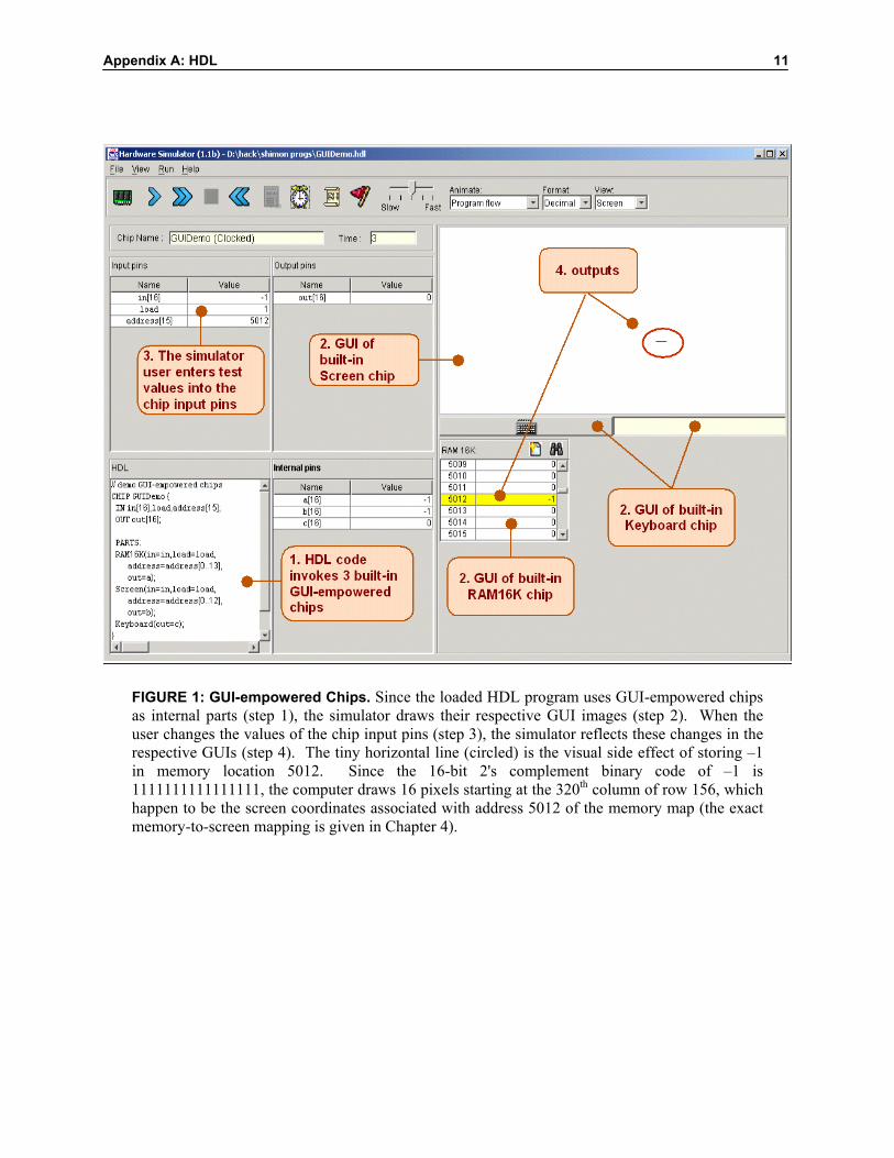
Example: To illustrate how the simulator deals with GUI-empowered chips, consider the following HDL program, which uses the built-in chips RAM16K, Screen, and Keyboard:
// Demo of GUI-empowered chips. // The logic of this chip is meaningless, and is used merely to // force the simulator to display some GUI-empowered chips. CHIP GUIDemo { IN in[16],load, address[15]; OUT out[16]; PARTS: RAM16K(in=in,load=load,address=address[0..13],out=a); Screen(in=in,load=load,address=address[0..12],out=b); Keyboard(out=c); }
The chip logic feeds the 16-bit in value into two destinations: register number address in the RAM16K chip and register number address in the Screen chip (presumably, the HDL programmer who wrote this code has figured out the widths of these address pins from the API's of these chips). In addition, the chip logic routes the value of the currently pressed keyboard key to the internal pin c. These meaningless operations are designed for one purpose only: illustrating how the simulator deals with built-in GUI-empowered chips. The actual impact is shown in Figure 1.
Appendix A: HDL 11
FIGURE 1: GUI-empowered Chips. Since the loaded HDL program uses GUI-empowered chips as internal parts (step 1), the simulator draws their respective GUI images (step 2). When the user changes the values of the chip input pins (step 3), the simulator reflects these changes in the respective GUIs (step 4). The tiny horizontal line (circled) is the visual side effect of storing –1 in memory location 5012. Since the 16-bit 2's complement binary code of –1 is 1111111111111111, the computer draws 16 pixels starting at the 320th column of row 156, which happen to be the screen coordinates associated with address 5012 of the memory map (the exact memory-to-screen mapping is given in Chapter 4).
Appendix A: HDL 12
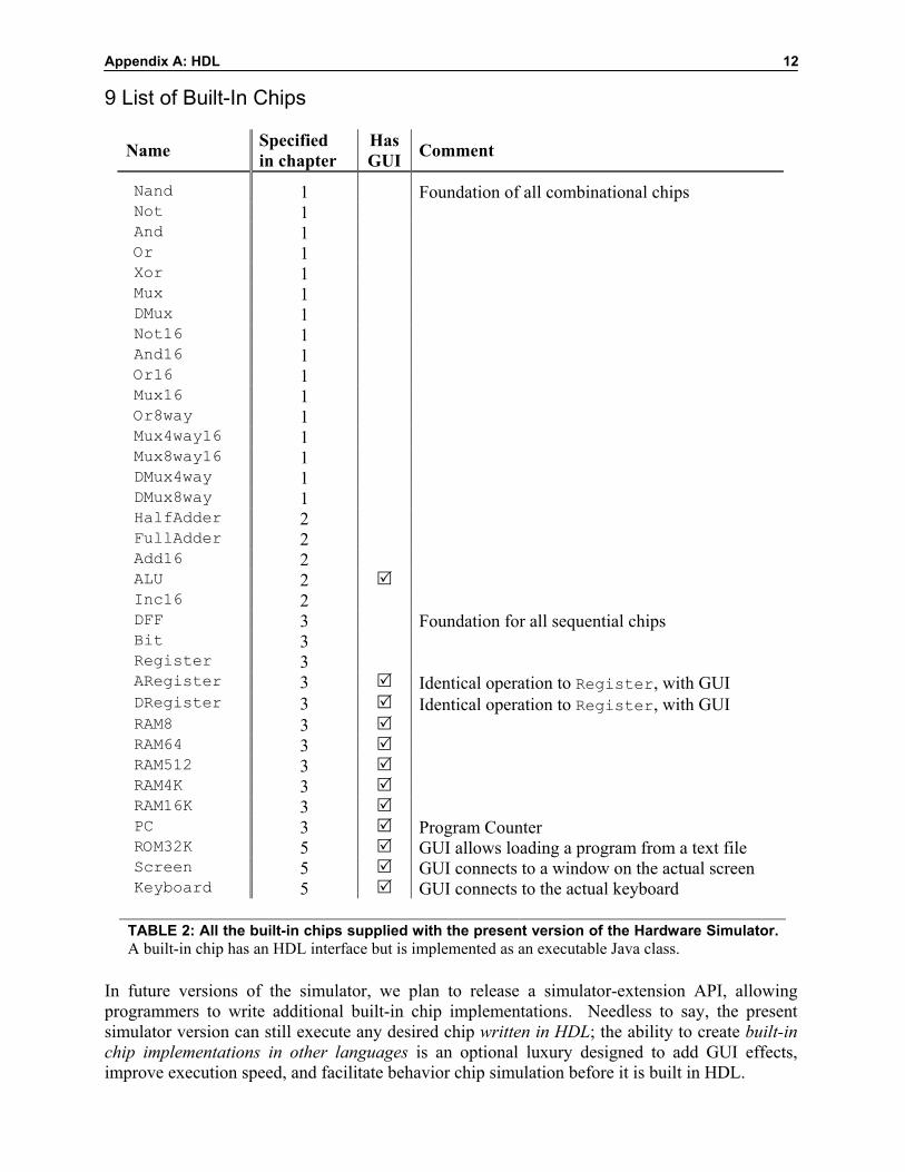
9 List of Built-In Chips
Name Specified in chapter
Has GUI Comment
Nand 1 Foundation of all combinational chips Not 1 And 1 Or 1 Xor 1 Mux 1 DMux 1 Not16 1 And16 1 Or16 1 Mux16 1 Or8way 1 Mux4way16 1 Mux8way16 1 DMux4way 1 DMux8way 1 HalfAdder 2 FullAdder 2 Add16 2 ALU 2 Inc16 2 DFF 3 Foundation for all sequential chips Bit 3 Register 3 ARegister 3 Identical operation to Register, with GUI DRegister 3 Identical operation to Register, with GUI RAM8 3 RAM64 3 RAM512 3 RAM4K 3 RAM16K 3 PC 3 Program Counter ROM32K 5 GUI allows loading a program from a text file Screen 5 GUI connects to a window on the actual screen Keyboard 5 GUI connects to the actual keyboard
TABLE 2: All the built-in chips supplied with the present version of the Hardware Simulator. A built-in chip has an HDL interface but is implemented as an executable Java class.
In future versions of the simulator, we plan to release a simulator-extension API, allowing programmers to write additional built-in chip implementations. Needless to say, the present simulator version can still execute any desired chip written in HDL; the ability to create built-in chip implementations in other languages is an optional luxury designed to add GUI effects, improve execution speed, and facilitate behavior chip simulation before it is built in HDL.