appendix a the first prototype of the phase alignment concept978-1-4020-8062-3/1.pdf · the first...
TRANSCRIPT
Appendix AThe First Prototype of the Phase Alignment Concept
The first realization of the phase alignment concept is a discrete-component prototype [42],designed to work at a carrier frequency of 250MHz. Only the parts of a Cartesian feedback systemneeded to test phase alignment, namely the upconverter, downconverter, and power amplifier,are assembled.
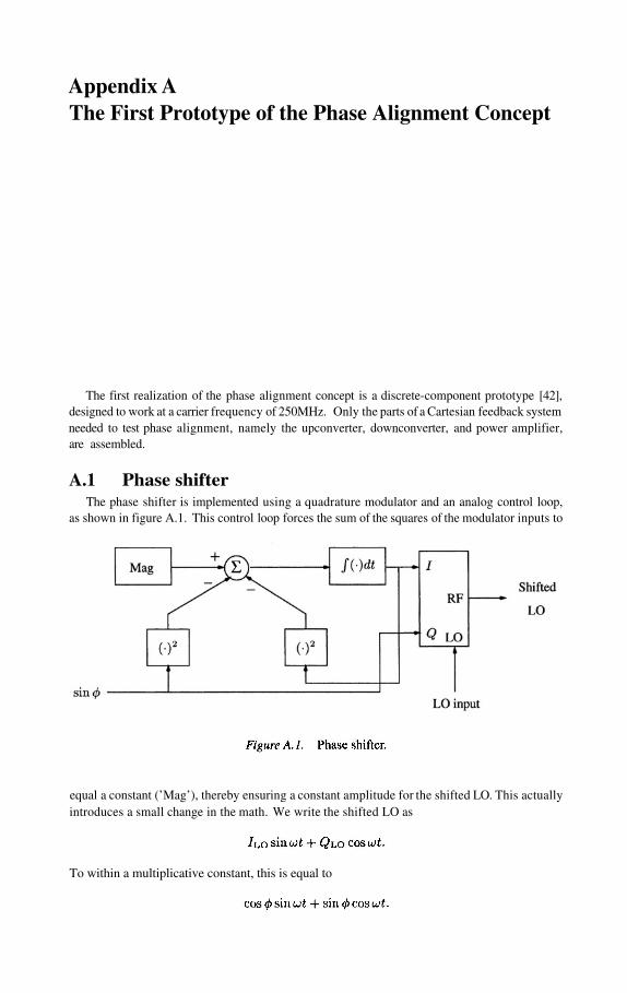
A.1 Phase shifterThe phase shifter is implemented using a quadrature modulator and an analog control loop,
as shown in figure A.1. This control loop forces the sum of the squares of the modulator inputs to
equal a constant (’Mag’), thereby ensuring a constant amplitude for the shifted LO. This actuallyintroduces a small change in the math. We write the shifted LO as
To within a multiplicative constant, this is equal to

118 FEEDBACK LINEARIZATION OF RF POWER AMPLIFIERS
For this prototype, then, the analog input is proportional to the sine of the phase shift. A functionalblock labeled ’arcsin(·)’ effectively exists between the integrator output and phase shifter input.
The implemented phase shifter is shown in figure A.2. Because of the squaring functional
blocks, there are in general two values of that would satisfy the control loop. The sign ofthe incremental gain around the loop is positive for one solution and negative for the other. Thecomparator in figure A.2 ensures stability by switching the sign of the loop gain based on thecurrent value of
The switches on all of the integrators are purely for testing purposes and are manually operated.These familiar “3-mode integrators” allow the outputs of the integrators to be held at their lastvalue, to be manually adjusted with potentiometers, or to operate normally as integrators.
A.2 Phase error and integratorThe phase alignment system core, shown in figure A.3, represents a straightforward mapping
from the concept of chapter 4 to op-amp building blocks. For reasons discussed in that chapter,it is necessary to trim the output offsets of the AD835 multipliers (from Analog Devices). Thistrimming is crudely accomplished via a potentiometer connected to the summing input of oneof the multipliers.
A.3 Test resultsThe prototype shown in figures A.2 and A.3 is built and tested in a 250 MHz RF system.
Figure A.4 shows the test setup. Off-the-shelf discrete components are used for the mixers,and the amplifier is the HP8347 bench-top, leveled-power amplifier. Not shown is a resistivevoltage divider at the input of the downconversion mixer. An additional phase shifter is insertedin the control path and is manually controlled. By varying this phase shift, we simulate driftnormally due to temperature and aging. Figure A.5 shows the outcome of this experiment. TheI channel is driven with a 50mV sinusoid, and the Q channel is grounded. It can be seen that

Appendix A: The First Prototype of the Phase Alignment Concept 119
our prototype automatically and continuously compensates for misalignments as large as ±88degrees. Alignment to within 3.8 degrees is maintained over this entire range of disturbances.
Figure A.6 shows system performance as the frequency of the input sinusoid is varied. It isseen that performance deteriorates rapidly above 2 MHz. This is due to the op-amp used to buildthe subtractor (National Semiconductor’s LMC6484), which has a gain-bandwidth product of1.5MHz.

120 FEEDBACK LINEARIZATION OF RF POWER AMPLIFIERS
The following table 1 compares the prototype with other examples from the literature.
1Accuracy value for Ohishi et al. is inferred.

Appendix A: The First Prototype of the Phase Alignment Concept 121

Appendix BThe Experimental Setup for CFB IC
This appendix describes the test board for the fully integrated prototype. The final board isfairly large, measuring approximately 8x9 inches. It has three layers of interconnect. The upperand lower layers are used for ordinary traces, while the middle layer is a ground plane.
B.1 Single-ended-to-differential conversionAll of the critical analog signals on the IC are fully differential. This complicates the testing
somewhat, as test instruments in the laboratory normally provide (and accept) single-endedsignals. It is therefore necessary to convert between single-ended and differential signals at theboard level.
Further complicating the design is that it is desirable to use DC and low-frequency inputsignals, making it impossible to use an ordinary transformer. Figure B. 1 shows the design solutionfor single-ended-to-differential conversion used on the test board (labeled “S/D” in figure B.3).Nominally, the common-mode level for baseband differential signals is 1.25V. Trimming toachieve this level is done by varying the resistor indicated in figure B.1. The predistortion inputson the chip actually require an S/D converter with two special characteristics: the common-modelevel needed is 1.75 V, and the output resistance of the converter needs to match that of the on-chipdriver used for closed-loop operation. The resistor values for this S/D converter are chosen tosatisfy these two constraints.
Differential-to-single-ended conversion is a simpler problem, involving two op-amps as volt-age buffers and one op-amp to perform a subtraction. These D/S converters nominally drive thecapacitive inputs of an oscilloscope. Here the choice of the LM6134 op-amp proves challeng-ing, as it is designed with unusually low stability margins. Efforts at compensation aside, it isultimately necessary to configure the oscilloscope such that it presents a resistive, load tothe D/S output.
B.2 Clock referenceFigure B.2 shows the crystal oscillator circuit used to provide a stable clock reference.
Complicating this normally straightforward design is that the only crystal oscillators availablecurrently are for 5V or 3.3V supplies, while the IC operates off a 2.5V supply. Not wishing toadd yet another supply line to the board, we make do with the ±2.5V supply already available.

124 FEEDBACK LINEARIZATION OF RF POWER AMPLIFIERS
The transformer in figure B.2 exploits the fact that if the oscillator output has a peak-to-peakamplitude of 5V, each of the balanced outputs on the secondary side will have peak-to-peakamplitudes of 2.5V. The center tap of the secondary winding is biased by the potentiometer suchthat the actual clock output of this circuit swings between ground and 2.5V.
B.3 Overview of test boardA simplified diagram of the test board is shown in figure B.3. The “monitor” signals, Imonitor
and Qmonitor, are used to monitor the baseband inputs to the upconverter mixers. These are the“predistortion inputs” of figures 5.39 and 5.40, for example. The nominal values for the voltage

Appendix B: The Experimental Setup for CFB IC 125
supplies to the board are as follows: Vdd is 2.5, Ddrain and cascode bias are 2.1V, driver bias is1.1V, the (upconversion) mixer supply is 3.5V, and the PA drains are biased at 2.0V. As noted insection B.2, a -2.5V supply is also available for various board-level components.

References
[1] H. S. Black, “Stabilized feedback amplifiers,” Bell System Technical Journal, vol. 13, pp.1–18, 1934.
[2] H. W. Bode, Network Analysis and Feedback Amplifier Design, Van Nostrand, New York,1945.
[3] J. K. Roberge, Operational Amplifiers: Theory and Practice, John Wiley and Sons, Inc.,New York, New York, 1975.
[4] J.L. Dawson, S. Boyd, M. Hershenson, and T.H. Lee, “Optimal allocation of local feedbackin multistage amplfiers via geometric programming,” IEEE Transactions on Circuits andSystems–I: Fundamental Theory and Applications, vol. 48, pp. 1–11, January 2001.
[5] S. Boyd and L. Vandenberghe, “Introduction to convex optimization with engineeringapplications,” Course Notes, 1997, http://www.stanford.edu/class/ee364/.
[6] J. Ecker, “Geometric programming: methods, computations and applications,” SIAMRev., vol. 22, no. 3, pp. 338–362, 1980.
[7] Y. Nesterov and A. Nemirovsky, Interior-point polynomial methods in convex program-ming, vol. 13 of Studies in Applied Mathematics, SIAM, Philadelphia, PA, 1994.
[8] P. R. Gray and R. G. Meyer, Analysis and Design of Analog Integrated Circuits, JohnWiley and Sons, New York, NY, 1993.
[9] W. M. Siebert, Circuits, Signals, and Systems, The MIT Press, Cambridge, MA, 1993.
[10] T. H. Lee, The Design of CMOS Radio-Frequency Integrated Circuits, Cambridge Uni-versity Press, New York, NY, 1998.
[11] R. J. Duffin, E. L. Peterson, and C. Zener, Geometric Programming — Theory andApplications, Wiley, 1967.
[12] M. Hershenson, S. Boyd, and T. H. Lee, “GPCAD: A tool for CMOS op-amp synthesis,”in IEEE/ACM International Conference on Computer Aided Design, San Jose, CA, 1998,pp. 296–303.

128 REFERENCES
[13] M. Hershenson, S. P. Boyd, and T. H. Lee, “Automated design of folded-cascode op-amps with sensitivity analysis,” in International Conference on Electronics, Circuits andSystems, September 1998, vol. 1, pp. 1–1.
[14] M. Hershenson, S. Mohan, S. Boyd, and T. H. Lee, “Optimization of inductor circuits viageometric programming,” in Design Automation Conference, 1999, pp. 994–998.
[15] K. O. Kortanek, X. Xu, and Y. Ye, “An infeasible interior-point algorithm for solvingprimal and dual geometric progams,” Mathematical Programming, vol. 76, no. 1, pp.155–181, 1997.
[16] M. Hershenson, S. Boyd, and T. H. Lee, “Optimal design of a CMOS op-amp via geometricprogramming,” in Applied and Computational Control, Signals, and Circuits, B. Datta,Ed., vol. 2. Birkhauser, 2000.
[17] W. J. Rugh, Nonlinear System Theory: The Volterra/Wiener Approach, The Johns HopkinsUniversity Press, Baltimore, Maryland, 1981.
[18] M.Johansson, “Linearization of RF power amplifiers using Cartesian feedback,” Tech.Rep., Lund University, 1991, Thesis for the degree of Teknisk Licentiat.
[19] R. C. Tupynamba and E. Camargo, “MESFET nonlinearities applied to predistortionlinearizer design,” in IEEE MTT-S Digest, 1992, pp. 955–958.
[20] N. Imai, T. Nojima, and T. Murase, “Novel linearizer using balanced circulators and itsapplication to multilevel digital radio systems,” IEEE Transactions Microwave Theoryand Techniques, vol. 37, pp. 1237–1243, 1989.
[21] G. Karam and H. Sari, “Implementation and performance of data predistortion with mem-ory in digital microwave radio,” in Proceeding of the IEEE Global TelecommunicationsConference (GLOBECOM), 1989, vol. 1, pp. 400–405.
[22] H.W. Kang, Y.S. Cho, and D.H. Youn, “On compensating nonlinear distortions of anOFDM system using an efficient adaptive predistorter,” IEEE Transactions on Commu-nications, vol. 47, pp. 522–526, 1999.
[23] B. Razavi, RF Microelectronics, Prentice-Hall, Inc., Upper Saddle River, NJ, 1998.
[24] A.A.M. Saleh and D. Cox, “Improving the power-added efficiency of FET amplifiersoperating with varying-envelope signals,” IEEE Transactions on Microwave Theory andTechniques, vol. 83, pp. 51–56, 1983.
[25] D. Su and W. McFarland, “An IC for linearizing RF power amplifiers using envelopeelimination and restoration,” in ISSCC Digest of Technical Papers, 1998, pp. 54–55.
[26] P. Nagle, P. Burton, E. Heaney, and F. McGrath, “A wide-band linear amplitude modulatorfor polar transmitters based on the concept of interleaving delta modulation,” IEEE Journalof Solid-State Circuits, vol. 37, pp. 1748–1756, 2002.
[27] D.C. Cox, “Linear amplification with nonlinear devices,” U.S. Patent # 3,777,275, De-cember 4, 1973.
[28] D.C. Cox, “Linear amplification with nonlinear components,” IEEE Transactions onCommunications, vol. COM-22, pp. 1942–1945, 1974.

REFERENCES 129
[29] D.C. Cox and R.P. Leck, “A VHF implementation of a LINC amplifier,” IEEE Transactionson Communications, vol. COM-24, pp. 1018–1022, 1976.
[30] Majid Boloorian and Joseph McGeehan, “The frequency-hopped Cartesian feedbacklinear transmitter,” IEEE Trans. on Vehicular Technology, vol. 45, pp. 688–706, 1996.
[31] M. Johansson and L. Sundström, “Linearisation of RF multicarrier amplifiers usingCartesian feedback,” Electronics Letters, vol. 30, pp. 1110–1111, 1994.
[32] A. Bateman, D. Haines, and R. Wilkinson, “Linear transceiver architectures,” in IEEEConference on Vehicular Technology, 1988, pp. 478–484.
[33] M. Johansson and L. Sundström, “Linearised high-efficiency power amplifier for PCN,”Electronics Letters, vol. 27, pp. 762–764, 1991.
[34] M. Briffa and M. Faulkner, “Gain and phase margins of Cartesian feedback RF amplifierlinearisation,” Journal of Electrical and Electronics Engineering, Australia, vol. 14, pp.283–289, 1994.
[35] M. Briffa and M. Faulkner, “Dynamically biased Cartesian feedback linearization,” inProceedings of the 1993 IEEE Vehicular Technology Conference, 1993, pp. 672–675.
[36] Y. Ohishi, M. Minowa, E. Fukuda, and T. Takano, “Cartesian feedback amplifier withsoft landing,” in 3rd IEEE International Symposium on Personal, Indoor, and WirlessCommunications, 1992, pp. 402–406.
[37] M. Faulkner, D. Contos, and M. Briffa, “Performance of automatic phase adjustment usingsupply current minimization in a RF feedback lineariser,” in The 8th IEEE InternationalSymposium on Personal, Indoor, and Mobil Radio Communications, 1997, pp. 858–862.
[38] D. Cox, “Linear amplification by sampling techniques: A new application for deltacoders,” IEEE Transactions on Communications, vol. COM-23, pp. 793–798, 1975.
[39] G. Han and E. Sánchez-Sinencio, “CMOS transconductance multipliers: A tutorial,” IEEETransactions on Circuits and Systems-II, vol. 45, pp. 1550–1563, 1998.
[40] A. Bakker, K. Thiele, and J. Huijsing, “A CMOS nested chopper instrumentation amplifierwith 100nV offset,” in ISSCC Digest of Technical Papers, 2000, pp. 156–157.
[41] Q. Huang and C. Menolfi, “A 200nV offset noise PSD 5.6kHz chopperinstrumentation amplifier in 1µm digital CMOS,” in ISSCC Digest of Technical Papers,2001, pp. 362–363.
[42] J.L. Dawson and T.H. Lee, “Automatic phase alignment for high bandwidth Cartesianfeedback power amplifiers,” in IEEE Radio and Wireless Conference, 2000, pp. 71–74.
[43] J.L. Dawson and T.H. Lee, “Automatic phase alignment for a fully integrated CMOSCartesian feedback power amplifier system,” in ISSCC Digest of Technical Papers, 2003,pp. 262–263.
[44] S.M. McBeath, D.T. Pinckley, and J.R. Cruz, “W-CDMA power amplifier modeling,” inProceedings of the IEEE Vehicular Technology Conference, 2001, vol. 4, pp. 2243–2247.
130 REFERENCES
[45] C.P. Silva, C.J. Clark, A. A. Moulthrop, and M.S. Muha, “Optimal-filter approach fornonlinear power amplifier modeling and characterization,” in IEEE MTT-S Symposium,2000, pp. 437–440.
[46] S. Watanabe, “Power amplifier modeling issues and advancement in Japan,” in Proceed-ings of the IEEE GaAs IC Symposium, 1999, pp. 69–72.
[47] D. K. Choi and S. I. Long, “A physically based analytic model of FET class-E poweramplifiers–designing for maximum PAE,” IEEE Transactions on Microwave Theory andTechniques, vol. 47, no. 9, pp. 1712–1720, September 1999.
[48] C. Clark, G. Chrisikos, M. Muha, A. Moulthrop, and C. Silva, “Time-domain envelopemeasurement technique with application to wideband power amplifier modeling,” IEEETransactions on Microwave Theory and Techniques, vol. 46, no. 12, pp. 2531–2540,December 1998.
[49] M.Honkanen, O.Pöllänen, J. Tanskanen, E. Järvinen, and S. Häggman, “Comparisonof measured and simulated adjacent channel power using a functional highpower amplifier model,” in Proceedings of the IEEE Vehicular Technology Conference,May 1998, vol. 3, pp. 2459–2463.
[50] M. Honkanen and S. Häggman, “New aspects on nonlinear power amplifier modeling inradio communication system simulations,” in Proceedings of the 8th IEEE InternationalWireless Symposium on Personal, Indoor, and Wireless Communications, 1998, vol. 3, pp.844–848.
[51] R. Achatz, R. Dalke, and Y. Lo, “Power amplifier model for optimizing battery current,interference, and link margin,” in Proceedings of the IEEE International Symposium onElectromagnetic Compatibility, 1998, pp. 434–438.
[52] A. Bernardini and S. De Fina, “Application of neural waveform predistortion to experi-mental TWT data,” in Proceedings of the 6th Mediterranean Electrotechnical Conference,1991, pp. 468–471.
[53] K. Nagaraj, J. Vlach, T. R. Viswanathan, and K. Singhal, “Switched-capacitor integratorwith reduced sensitivity to amplifier gain,” Electronics Letters, vol. 22, pp. 1103–1105,October 1986.
[54] P. Gray and R. Meyer, “MOS operational amplifier design–a tutorial overview,” IEEEJournal of Solid-State Circuits, vol. SC-17, no. 6, pp. 969–982, December 1982.
[55] T.C. Choi, R. T. Kaneshiro, R. W. Brodersen, P. R. Gray, W. B. Jett, and M. Wilcox, “High-frequency CMOS switched-capacitor filters for communications application,” IEEE Jour-nal of Solid-State Circuits, vol. SC-18, pp. 652–664, December 1983.
[56] K. Bult and G. Geelen, “A fast-settling CMOS op-amp for SC circuits with 90-dB DCgain,” IEEE Journal of Solid-State Circuits, vol. SC-25, pp. 1379–1384, December 1990.
[57] R. Gregorian and G. Temes, Analog MOS Integrated Circuits for Signal Processing, WileySeries on Filters: Design, Manufacturing, and Applications. John Wiley and Sons, Inc.,NY, NY, 1986.
[58] T.B. Cho and P.R. Gray, “A 10 b, 20 Msample/s, 35 mW pipeline A/D converter,” IEEEJournal of Solid-State Circuits, vol. 30, pp. 166–172, March 1995.

REFERENCES 131
[59] M. Pelgrom, A. Duinmaijer, and A. Welbers, “Matching properties of MOS transistors,”IEEE Journal of Solid-State Circuits, vol. 24, pp. 1433–1440, 1989.
[60] J. Crols and M. Steyaert, “A 1.5 GHz highly linear CMOS downconversion mixer,” IEEEJournal of Solid-State Circuits, vol. 30, pp. 736–742, July 1995.
[61] S. Galal, M. Tawfik, and H. Ragaie, “On the design and sensitivity of RC sequenceasymmetric polyphase networks in RF integrated transceivers,” in Proceedings of the1999 IEEE International Symposium on Circuits and Systems (ISCAS), July 1999, vol. 2,pp. 593–597.
[62] S. Galal, H. Ragaie, and M. Tawfik, “RC sequence asymmetric polyphase networks forRF integrated transceivers,” IEEE Transactions on Circuits and Systems–II: Analog andDigital Signal Processing, vol. 47, pp. 18–27, January 2000.

Index
aliasingof chopping artifacts, 76
analog multiplicationchopper stabilization for, 52limits on performance, 55offset-free, 52
battery lifetime, 2bottom plate sampling, 76
capacitive dividerto sense PA output, 95
Cartesian feedback, 41and root locus analysis, 47as a predistorter, 58, 59, 102bandwidth limitation, 58fundamental strength, 57historical limitations, 57stability analysis, 45
CFB IC project, 57motivation for, 60system diagram, 62test board, 123
chopper stabilization, 52choppers, 70chopping frequency, 76CMOS, 1compensation
for large phase misalignments, 46constant-gm bias current, 100convex optimization, 14
die photo, 102downconverter problems, 103dynamic biasing, 39
EER, 39efficiency
tradeoff with linearity, 33envelope elimination and restoration, 39
feedforward linearization, 38folding amplifier, 81
geometric programming, 14geometric programs, 6, 14
convex form of, 15form, 14immunity to local extrema, 16solving, 15
high-performance, 2
integrator, 713-mode, 74, 118autozeroing, 71, 75clock signal for, 77for continuous-time control, 76switched-capacitor, 71, 75
LINC, 40linear modulation, 2linearity
in transmitters, 2tradeoff with efficiency, 33
linearization circuitry, 88current draw, 102performance, 102
linearization techniques, 35local feedback allocation
problem of, 6relevance to power amplifiers, 32
local feedback andbandwidth, 11, 17delay, 12, 18dynamic range, 12, 18gain, 9, 16IIP3, 13noise, 12, 18

134 REFERENCES
nonlinearity, 10rise-time, 12, 18sensitivity, 17SFDR, 13, 18source degeneration, 27swing, 9, 16
loop driver amplifiers, 89in predistort mode, 92
loop dynamicsuncompensated, 105under dominant-pole compensation, 104under slow-rolloff compensation, 105user-controllable, 91, 104
loop filter, 89
matrix multiplication, 63, 82, 92mixer
downconversion, 95upconversion, 93
mixersquadrature error in, 51
monomialform of, 14
multiplier cell, 66analysis of, 67
multiplier offsets, 51
nonlinear system theory, 35relevance to power amplifiers, 35
offset trim, 97, 103op-amp
externally compensated, 91folded cascode, 72for downconversion mixer, 97fully differential, 72gain-boosted, 72single-ended, 73
phase alignment regulator, 48key relation, 49stability, 50
phase alignment systemcurrent draw, 84
discrete-component prototype, 117overview diagram, 84performance, 85
phase misalignment, 45by 90 degrees, 46impact on stability, 45, 88
phase shifting, 63the local oscillator, 63, 117
polar feedback, 35polyphase filters, 99portability, 1postdistortion, 36posynomial
form of, 14power amplifier, 1
circuit, 93importance of, 2
power amplifier modeling, 57power backoff, 35power dissipation
of CFB IC, 102predistortion, 36
adaptive, 37
return differences, 8
sample-and-hold, 76slow-rolloff compensation, 47
root locus techniques, 47subtraction, 89summing junction, 89symbol rotation, 49, 63
approximating sin and cos, 63using the 1-norm, 64, 78
testability, 73testing, 80, 85, 86, 102, 103transceivers
expectations of, 1transconductance cell, 80
analysis of, 80
Volterra series, 35