application of iddt test in sram arrays towards detection ... · dizerta cn a pr aca bola...
TRANSCRIPT

SLOVENSKA TECHNICKA UNIVERZITA V BRATISLAVEFakulta elektrotechniky a informatiky
Ustav elektroniky a fotoniky
Application of IDDT Test in SRAM ArraysTowards Detection of Weak Opens
Aplikacia IDDT testu na pokrytie prerusenı v SRAM poliach
Autoreferat dizertacnej pracena zıskanie vedecko-akademickej hodnosti Philosophiae Doctor (PhD.)
v odbore doktorandskeho studia: 26-13-9 Elektronikav specializacii: Mikroelektronika
Evidencne cıslo: FEI-10843-10437
autor: Ing. Gabor Gyepesskolitel’ka: prof. Ing. Viera Stopjakova, PhD.
Bratislava, maj 2014

Dizertacna praca bola vypracovana na Ustave elektroniky a fotoniky Fakultyelektrotechniky a informatiky Slovenskej technickej univerzity v Bratislave.
doktorand: Ing. Gabor GyepesUstav elektroniky a fotonikyFakulta elektrotechniky a informatikySlovenska technicka univerzita v BratislaveIlkovicova 3, 812 19 Bratislava
skolitel’ka: prof. Ing. Viera Stopjakova, PhD.Ustav elektroniky a fotonikyFakulta elektrotechniky a informatikySlovenska technicka univerzita v BratislaveIlkovicova 3, 812 19 Bratislava
oponenti: doc. RNDr. Elena Gramatova, PhD.Fakulta informatiky a informacnych technologiıSlovenska technicka univerzita v BratislaveUstav pocıtacovych systemov a sietıIlkovicova 2, 842 16 Bratislava
doc. Ing. Jirı Jakovenko, PhD.Fakulta elektrotechnickaCeske vysoke ucenı technicke v PrazeKatedra mikroelektronikyTechnicka 2, 166 27 Praha 6
Autoreferat bol rozoslany dna: . . . . . . . . . . . . . . . . . .Obhajoba dizertacnej prace sa kona dna . . . . . . . . . . . . . . . . . . . . . o . . . . . . . . . hod. naFakulte elektrotechniky a informatiky Slovenskej technickej univerzity, Ilkovicova3, 812 19 Bratislava, pred komisiou pre obhajoby dizertacnych prac v odboredoktorandskeho studia 26-13-9 Elektronika.
Predseda odborovej komisieprof. Ing. Daniel Donoval, DrSc.FEI STU, Ilkovicova 3812 19 Bratislava

Contents
Introduction 2
1 Background 3
2 Research objectives 6
3 IDDT test implementation 7
3.1 Test patterns for IDDT test . . . . . . . . . . . . . . . . . . . . . . . . . . . . . . . 7
3.2 Design for IDDT testability . . . . . . . . . . . . . . . . . . . . . . . . . . . . . . . 8
3.2.1 CUT partitioning for IDDT test . . . . . . . . . . . . . . . . . . . . . . . . 8
3.2.2 Partitioning of the SRAM array . . . . . . . . . . . . . . . . . . . . . . . . 10
3.3 Open defects in an SRAM cell . . . . . . . . . . . . . . . . . . . . . . . . . . . . . 12
3.4 Conceptual approach to IDDT . . . . . . . . . . . . . . . . . . . . . . . . . . . . . 13
3.4.1 An obvious approach . . . . . . . . . . . . . . . . . . . . . . . . . . . . . . 13
3.4.2 The proposed delta approach . . . . . . . . . . . . . . . . . . . . . . . . . 14
4 Experimental results 16
4.1 The most efficient IDDT parameter . . . . . . . . . . . . . . . . . . . . . . . . . . . 16
4.2 Efficiency analysis in two different technologies . . . . . . . . . . . . . . . . . . . . 18
4.3 The effect of sensor hardware on IDDT . . . . . . . . . . . . . . . . . . . . . . . . . 19
4.4 The effect of parasitics and leakage current on IDDT . . . . . . . . . . . . . . . . . 23
5 Achieved results and their asset 28
6 Conclusion 30
Author’s publications 32
References 35
1
Introduction
The high scale integration of integrated circuits (IC) would not be possi-
ble without the evolution of technologies, where the dimensions of components
are pushed often to minimum, even reaching material physical limitations. Un-
fortunately, advanced technologies are introducing significant drawbacks. One
important drawback is the presence of new defects and failure mechanisms, which
have a negative impact on both the process yield and IC reliability. Therefore,
the importance of IC testing is rapidly rising.
The increasing complexity of ICs requires new, sophisticated test methods. For
logic circuits, a functional test was sufficient. However, the conventional functional
test may fail in covering some catastrophic faults, which do not necessarily cause
faulty outputs of digital circuits [1]. Catastrophic defects such as resistive opens,
bridging defects and gate-oxide shorts mostly cause reliability issues, where open
defects with open resistance lower than 10 MΩ (considered as hard-detectable
defects) cannot be effectively unveiled by any functional test. Therefore, other
effective test alternatives like parametric test methods are developed.
Parametric test does not represent the main test approach; it is rather an
augmenting test method, which is meant to help to increase the reliability of a
tested IC. One of these parametric test approaches is the Transient supply current
measurement – IDDT test represents an interesting and challenging test method
that can be very efficient in detecting open defects. However, due the difficulties
associated with the practical realization of this method, it still seeks for its wider
acceptance.
Generally, IDDT test is well suited for repeating, regular structures because of
the homogeneity of the current consumption of identical parts in a tested system.
A good example of such a system are static random access memory (SRAM) ar-
rays, as it was also proved in [2]. Since SRAMs are the most often used embedded
memories, and in many cases, they may occupy more than 90% of the total silicon
area in a system-on-chip (SoC) [1, 3], they also represent the greatest reliability
fail factor in such systems.
2

1 Background
Current-based tests are already well known since the late 1980’s. In gen-
eral, these tests are divided in two major groups, IDDQ – the static or quiescent
current test [4] and IDDT – the dynamic or transient supply current test [5]. By
their nature, current-based test methods are referred to as parametric tests, and
are mostly used in CMOS technology, predominantly for logic circuits, although
application in analog circuits was also reported in [6, 7]. Current-based testing
has a great potential in detecting a device with catastrophic defects like opens,
floating gates, gate-oxide shorts and bridging defects. The supply current testing
is often used at the very beginning of a test process to rule out quickly defective
devices [8].
IDDQ testing has already found a practical usage, while IDDT test is still under
investigation, since it represents a rather great challenge to designers and test
engineers, mainly from the implementation point of view. In general, current-
based test approaches are well suited for ICs with uniform and repeating structures
[9].
Dynamic supply current testing is the subject of many researches and studies,
even though much less was published about IDDT testing then about IDDQ test.
The main idea of this approach is that during the process of switching, a CMOS
digital circuit draws a significant amount of supply current compared to the static
state of the same circuit. This part of the supply current is called the dynamic
(transient) or also switching current. In IDDT test approach, a circuit under test is
tested in its active state. Thus, by dynamic supply current test, the measurement
of the switching current of a tested digital circuit is meant [10]. The principle
of IDDT is presented in Fig. 1.1, where an open defect is present in a switching
CMOS inverter between the NMOS transistor and the ground (Fig. 1.1a) and the
dynamic current deviation (red waveform) is depicted in Fig. 1.1b. In this case,
the open defect causes reduction of the transient current pikes if compared to the
fault-free circuit, which is depicted with the dashed waveform.
The test decision criterion is based on one or more parameters of the observed
3

OpenDefect
ID
PMOS
NMOS
in out
(a) The placement of a
defect
DefectiveCurrent
time
IDIDDT current
(b) Increased dynamic current due to the
defect
Figure 1.1: The principle of IDDT test
dynamic current waveform. A typical IDDT waveform is depicted in Fig. 1.2a.
This current waveform can be characterized using several parameters, which may
change depending on the particular defect. These parameters include: current
waveform width (at a current value denoted Ilim, which is chosen carefully to
enable the reliable evaluation of the monitored parameter taking into account the
process variation), the charge provided by the waveform (integral of the waveform
with limits at Ilim), the peak value of the waveform, the peak time (time when
waveform reaches its peak value) and the average value of the waveform (for the
period of time, when the waveform crosses the current value Ilim).
T i m eP e a k t i m e
Powe
r sup
ply cu
rrent
A v e r a g e v a l u e
W i d t h
P e a k v a l u e
C h a r ge
I l i m
(a) Typical IDDT waveform
1 E 1 0 1 E 1 1 1 E 1 2
1 E - 8
1 E - 7
1 E - 6
1 E - 5
Amplit
ude [
A]
F r e q u e n c y [ H z ]
F r e q u e n c y s p e c t r u m o f I D D T
(b) Spectrum of the IDDT waveform
Figure 1.2: IDDT waveform characteristics
As already mentioned, there is no doubt that the dynamic supply current event
4

(Fig. 1.2a) is a very fast action. For example, the dynamic current of an SRAM
cell in a 90 nm technology might take less than 200 ps. In this case, the majority
of waveforms’ main harmonics are in the region of several GHz, as shown in
Fig. 1.2b. Thus, processing of such a signal is extremely difficult.
In general, current-based test approaches are well suited for ICs with uniform
and repeating structures [9], like SRAM arrays. The biggest advantage of IDDT
test is its ability to detect open defects, which are generally considered as hard-
detectable (if at all) types of physical defects. Additionally, the generation of test
vectors is relatively simple [11]. Though, for more complex logic circuits, inducing
IDDT current might get more complicated.
5
2 Research objectives
With the consideration of the actual needs and problems of SRAM testing,
the research objectives for this PhD thesis were stated as follows:
• Investigation of IDDT test as an augmenting method to extensive voltage-
based tests in SRAMs, based on the efficiency analysis of IDDT waveform
parameters in covering open defects. Definition of the most efficient param-
eter of IDDT waveform to be sensed.
• Definition and analysis of open faults in an SRAM cell, and their precise
fault models.
• Evaluation of feasibility of standard March tests for IDDT test of SRAMs, and
the definition of the minimum test sequence length of IDDT test.
• Proposal of IDDT test approach suited for SRAM arrays and its implementa-
tion in a deep-submicron technology.
• Investigation of on-chip versus off-chip measurement and processing, and
deriving of general “Design-for-IDDT-Testability” rules based upon test hard-
ware realization.
6
3 IDDT test implementation
3.1 Test patterns for IDDT test
The issue of generating test vectors for IDDT testing is investigated in [12].
Generating proper test vectors for a 6 transistor (6T) SRAM cell is not a difficult
task. The dynamic supply current appears when the SRAM changes its state.
There are two kinds of operations distinguished, the write process and the read
process. For us, important operations are transition write operations (the stored
value is overwritten) [13], which induce the IDDT current.
Since the SRAM cell is symmetric, two transition write operations of opposite
directions would activate the same defects in both inverters. This in practice
would mean that if the number of cells in an SRAM array is n, then the length of
the test would be 2n, since two transition write operations are required. Though,
before these write operations are performed it would be useful to know what
value is stored in the particular cell being written to. Hence, it would require an
additional read or write operation that increases the length of the test to 3n. Let
us assume that the first write operation which sets the first known value is the
write of a logic one (Log1 ).
In bit-oriented SRAMs, only one cell is investigated each time. Hence, theoret-
ically, where there is no need to check whether a given value was really stored in
the cell, the test length would be 3n. Obviously, with value check (read operation
after each write) the test length would grow to 6n. In a word-oriented SRAM
array, where the length of the word is m and no read operation is performed to
check for stored values, the address does not change for 2m + 1 operations. In
this case, the first write of Log1 can be carried out for the whole word and than,
only two operations are required to be performed on each bit in the word. In the
case of a read check, the length of the test of one word would become 4m + 2
long. This feature actually makes the IDDT test of word-oriented SRAMs shorter
in terms of March test length if both arrays have the same bit capacity.
7

Table 3.1: Example of March tests for a bit-oriented and a word-oriented SRAM
SRAM type March test solution Test length
Bit-oriented
(n bits)
m(w0, w1) 2n
m(w1, w0, w1) 3n
m(w1, r1, w0, r0, w1, r1) 6n
Word-oriented
(l words &
m bits/word)
m(w(01...1)m, w(11...1)m, w(10...1)m,
w(11...1)m, w(11...0)m, w(11...1)m)l(2m)
m(w(11...1)m, w(01...1)m, w(11...1)m,
w(10...1)m, w(11...1)m, w(11...0)m, w(11...1)m)l(2m+ 1)
m(w(11...1)m, r(11...1)m, w(01...1)m,
r(01...1)m, ..., w(11...1)m, r(11...1)m)l(4m+ 2)
3.2 Design for IDDT testability
The topology of IDDT test hardware mostly depends on monitored parameters
of the IDDT current, which are explained in section 1. The realization of current-
based test hardware can be divided into three major groups:
• On-chip test hardware
• Hybrid test hardware
• Off-chip test hardware
In the case of IDDT test, a special kind of design for testability is used, which
is called Design for IDDT testability (DfIT). Some aspects of design for current
testability are dealt in [14]. The general approach to DfIT is depicted in Fig. 3.1a,
where there always should be a sensing element between the power terminal and
the circuit under test, and also some processing and evaluating units. The output
of the evaluating unit is a current signature (a logic value for instance).
3.2.1 CUT partitioning for IDDT test
On-chip implementation of IDDT test is a huge challenge because digital circuits
mostly have one or more common power supply rails, which distribute the power
to all the subsystems. Since IDDT test is based on the monitoring of the current
through power supply rails, it presents a problem to detect changes in the dynamic
current waveform for complex and large circuits, which result in a quite complex
design for IDDT testability.
8

CurrentSensor
CUT
CurrentSignature
(a) General approach to DfIT
Current sensor
Sensingelement
Processingunit
Evaluatingunit
Currentsignature
(b) Current sensor structure
Figure 3.1: Concept of DfIT
Input/OutputEcircuitry
VDD1 VDD2
Sen
sin
gEel
eme
nt
Add
ress
Edec
oder
s
Timingblock
MemoryEarray
Processingunit
Evaluatingunit
Output
Figure 3.2: DfIT for a SRAM based on power distribution
In Fig. 3.2, the layout of an SRAM circuit is depicted, which is organized based
upon the power distribution, where it is vital to separate the power rails of the
memory array and supporting circuits (address decoders, timing block, I/O). It
can be observed that the best solution is to divide the power rails (red lines)
outside the chip. From Fig. 3.2, one can also observe that VDD1 is the power
supply of supporting circuits, while VDD2 is the power supply pin of the SRAM
array. For test purposes, the two power supplies connected to the chip should be
completely separated, while for normal function the two inputs could be shorted.
Such partitioning of the tested circuit brings benefits for all three possibilities
of test hardware realizations. Nevertheless, in the case of completely off-chip
9
realization, the sensing element from Fig. 3.2 is placed between pin VDD2 and the
power supply, and the rest of the sensor is also placed outside the chip, which shall
be powered by VDD1 or a power supply different from VDD2. All three approaches
would need also extra output pins.
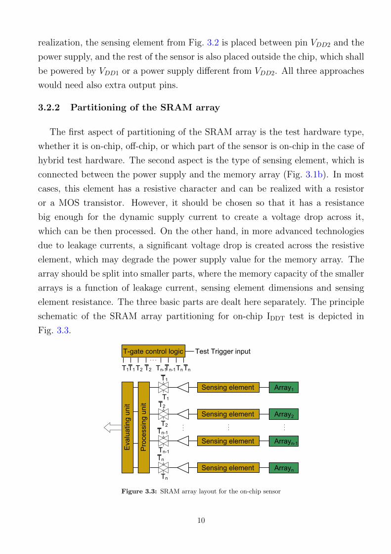
3.2.2 Partitioning of the SRAM array
The first aspect of partitioning of the SRAM array is the test hardware type,
whether it is on-chip, off-chip, or which part of the sensor is on-chip in the case of
hybrid test hardware. The second aspect is the type of sensing element, which is
connected between the power supply and the memory array (Fig. 3.1b). In most
cases, this element has a resistive character and can be realized with a resistor
or a MOS transistor. However, it should be chosen so that it has a resistance
big enough for the dynamic supply current to create a voltage drop across it,
which can be then processed. On the other hand, in more advanced technologies
due to leakage currents, a significant voltage drop is created across the resistive
element, which may degrade the power supply value for the memory array. The
array should be split into smaller parts, where the memory capacity of the smaller
arrays is a function of leakage current, sensing element dimensions and sensing
element resistance. The three basic parts are dealt here separately. The principle
schematic of the SRAM array partitioning for on-chip IDDT test is depicted in
Fig. 3.3.
Array1Sensing element
Array2Sensing element
Arrayn-1Sensing element
ArraynSensing element
Pro
cess
ing
unit
Eva
lua
ting
unit
T1
T2
Tn-1
Tn
T1
T2
Tn
Tn-1
T-gate control logic Test Trigger input
T1T1 T2T2 Tn-1Tn-1 TnTn
Figure 3.3: SRAM array layout for the on-chip sensor
10
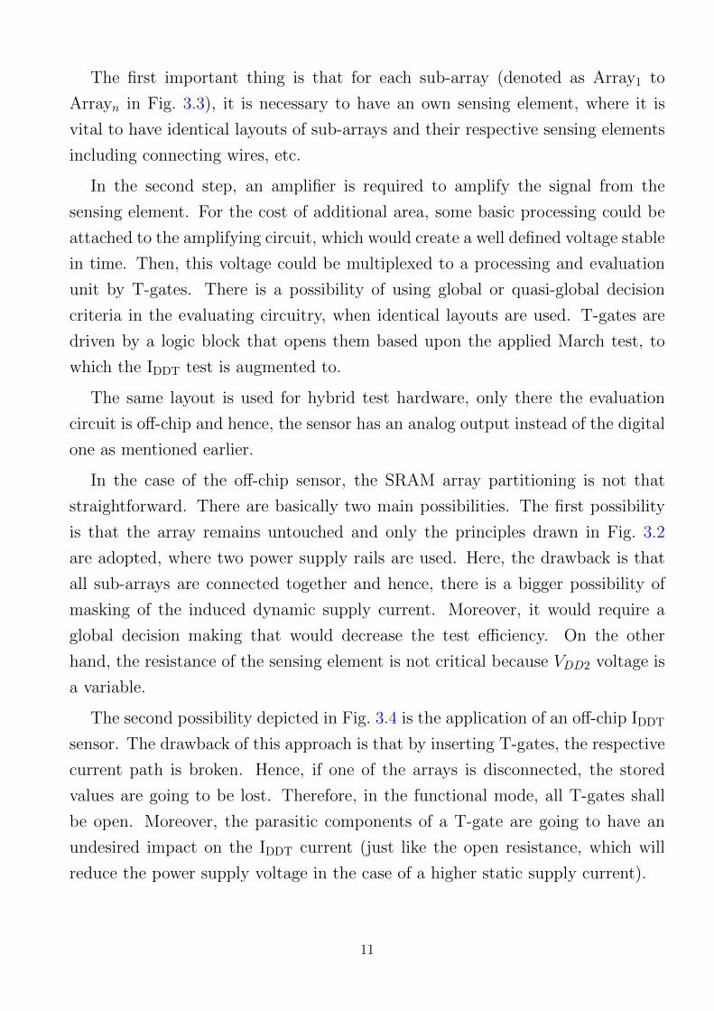
The first important thing is that for each sub-array (denoted as Array1 to
Arrayn in Fig. 3.3), it is necessary to have an own sensing element, where it is
vital to have identical layouts of sub-arrays and their respective sensing elements
including connecting wires, etc.
In the second step, an amplifier is required to amplify the signal from the
sensing element. For the cost of additional area, some basic processing could be
attached to the amplifying circuit, which would create a well defined voltage stable
in time. Then, this voltage could be multiplexed to a processing and evaluation
unit by T-gates. There is a possibility of using global or quasi-global decision
criteria in the evaluating circuitry, when identical layouts are used. T-gates are
driven by a logic block that opens them based upon the applied March test, to
which the IDDT test is augmented to.
The same layout is used for hybrid test hardware, only there the evaluation
circuit is off-chip and hence, the sensor has an analog output instead of the digital
one as mentioned earlier.
In the case of the off-chip sensor, the SRAM array partitioning is not that
straightforward. There are basically two main possibilities. The first possibility
is that the array remains untouched and only the principles drawn in Fig. 3.2
are adopted, where two power supply rails are used. Here, the drawback is that
all sub-arrays are connected together and hence, there is a bigger possibility of
masking of the induced dynamic supply current. Moreover, it would require a
global decision making that would decrease the test efficiency. On the other
hand, the resistance of the sensing element is not critical because VDD2 voltage is
a variable.
The second possibility depicted in Fig. 3.4 is the application of an off-chip IDDT
sensor. The drawback of this approach is that by inserting T-gates, the respective
current path is broken. Hence, if one of the arrays is disconnected, the stored
values are going to be lost. Therefore, in the functional mode, all T-gates shall
be open. Moreover, the parasitic components of a T-gate are going to have an
undesired impact on the IDDT current (just like the open resistance, which will
reduce the power supply voltage in the case of a higher static supply current).
11

Array1
Array2
Arrayn-1
Arrayn
T1
T2
Tn-1
Tn
T1
T2
Tn
Tn-1T
-gat
e co
ntr
ol lo
gic
Test Trigger input
T1
T1
T2
T2
Tn-1
Tn-1
Tn
Tn
Figure 3.4: Layout of the SRAM array for an off-chip IDDT test hardware
3.3 Open defects in an SRAM cell
According to [15], it is important to distinguish between possible locations
of resistive open defects in a 6T SRAM cell. In our work, the possible locations
of the resistive opens are derived from the ”wide” SRAM cell layout [3], where
opens were only considered in the metalization, vias, contacts and the polysilicon
layer.
In Fig. 3.5a, the transistor level schematic of a 6T SRAM cell is shown, where
possible locations of open defects are depicted. Since the 6T SRAM cell (Fig. 3.5a)
has a symmetrical topology and layout, there are altogether 21 (two times 9 plus
3 other) possible locations for opens. These opens were sorted into three groups,
based on their location.
Group I represents resistive opens, where both sides of the defect are con-
nected either to ground or the positive supply rail, and either directly or indirectly
through an open transistor. From Fig. 3.5a, O0, O1, O5, O8, and O11 belong to
this group. This type of resistive opens is illustrated by the open location denoted
as O0 in Fig. 3.5b, where the SRAM cell with the used open fault model in the
respective location is shown.
Group II represents open defects that have only one side connected to a well
defined potential. This happens when there is a gate of a transistor connected
12

WL
BL
nBL
M1M2
M3M4
M5M6
O1
O2
O3
O4
O5 O6'
O0
O8
O9O10
O11
O1'
O11'
O2' O3'
O4'
O5'
O6
O7O7'
O9'
(a) Possible opens in a ”wide” 6T SRAM cell
WL
BL
nBL
M1M2
M3M4
M5
M6
O4
Ropen0
CVDD
CGND
Ropen4
Ropen3O3
O0
(b) Open fault models used in 6T SRAM cell
Figure 3.5: The 6T SRAM cell
to the other side of an open defect. In this case, the potential on the transistor
gate is not well defined, and it is mainly given by the charge accumulated on the
parasitic capacitances between the gate side of the broken line and the surrounding
structures. The other electrodes of the parasitic capacitors are connected to a well
defined potential, which is either the positive or the negative supply rail. Hence,
all the parasitic capacitances are summed up, and are modeled by two capacitors.
From Fig. 3.5a, O2, O4, O9, and O10 belong to this group. In Fig. 3.5b, open
location denoted as O4 is an example of Group II defect.
Group III represents those open defects that have always well defined potential
on one side of the defect, while the potential of the other side is case dependent.
Opens denoted as O3, O6 and O7 belong to this group. The undefined side of open
defectO3 is connected to the drain of a pull-up transistor. Therefore, after start-up
condition, if the pull-up transistor is closed the potential of that side is unknown.
However, these open defects are investigated under no start-up condition and
hence, the same fault model defined for opens from Group I is used.
3.4 Conceptual approach to IDDT
3.4.1 An obvious approach
In a real case, decision is based on a fault-free tolerance band (TB), which is
based on two threshold values, which are gained from Monte Carlo (MC) analysis
13
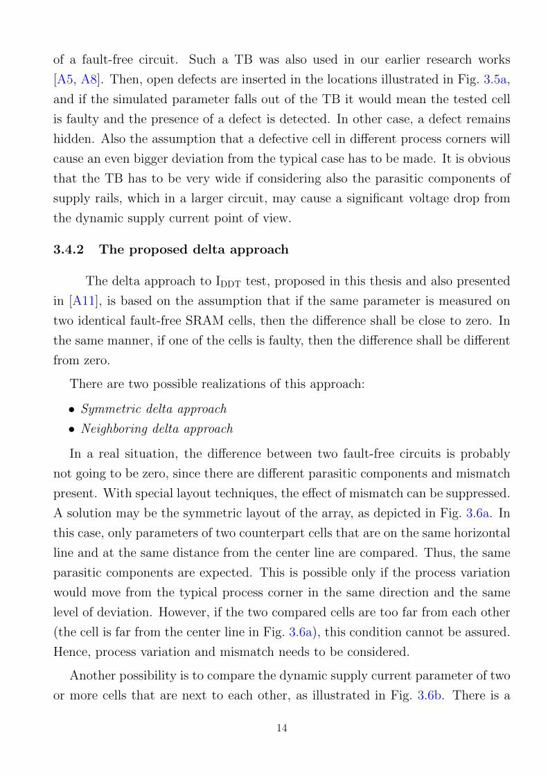
of a fault-free circuit. Such a TB was also used in our earlier research works
[A5, A8]. Then, open defects are inserted in the locations illustrated in Fig. 3.5a,
and if the simulated parameter falls out of the TB it would mean the tested cell
is faulty and the presence of a defect is detected. In other case, a defect remains
hidden. Also the assumption that a defective cell in different process corners will
cause an even bigger deviation from the typical case has to be made. It is obvious
that the TB has to be very wide if considering also the parasitic components of
supply rails, which in a larger circuit, may cause a significant voltage drop from
the dynamic supply current point of view.
3.4.2 The proposed delta approach
The delta approach to IDDT test, proposed in this thesis and also presented
in [A11], is based on the assumption that if the same parameter is measured on
two identical fault-free SRAM cells, then the difference shall be close to zero. In
the same manner, if one of the cells is faulty, then the difference shall be different
from zero.
There are two possible realizations of this approach:
• Symmetric delta approach
• Neighboring delta approach
In a real situation, the difference between two fault-free circuits is probably
not going to be zero, since there are different parasitic components and mismatch
present. With special layout techniques, the effect of mismatch can be suppressed.
A solution may be the symmetric layout of the array, as depicted in Fig. 3.6a. In
this case, only parameters of two counterpart cells that are on the same horizontal
line and at the same distance from the center line are compared. Thus, the same
parasitic components are expected. This is possible only if the process variation
would move from the typical process corner in the same direction and the same
level of deviation. However, if the two compared cells are too far from each other
(the cell is far from the center line in Fig. 3.6a), this condition cannot be assured.
Hence, process variation and mismatch needs to be considered.
Another possibility is to compare the dynamic supply current parameter of two
or more cells that are next to each other, as illustrated in Fig. 3.6b. There is a
14
Powersupply
(a) Symmetric delta approach
Powersupply
(b) Neighboring delta approach
Figure 3.6: Two possibilities of the delta approach
high probability that neighboring cells will have the same or very close process
variation.
One can never assure that at least one of the investigated cells will be fault-free.
Thus, this approach relies on probability calculation [16], which is based on the
fact that open defects are spot defects with random appearance. If only the delta
of two cells was considered in case of 2000 cells per array, it would mean that 23
dies out of a million samples will have at least one pair of counterparts with two
identical defects. This is true for the neighboring and symmetric delta as well. In
case of the neighboring delta approach if three cells were used, only in 90 cases
out of a billion would have identical defects.
15

4 Experimental results
4.1 The most efficient IDDT parameter
The most common SRAM cell is the 6T CMOS implementation, which
consists of two cross-coupled inverters formed by complementary transistor pairs
M1-M3 and M2-M4, and by two access transistors M5 and M6 that are usually
NMOS transistors, which ensure read and write access to the cell (Fig. 3.5b).
To ensure non-destructive read operation and reasonable noise margin, the Cell
Ratio (CR) (4.1) should be within the range from 1 to 2.5, where W denotes the
transistor channel width and L represents the transistor channel length. Larger
CR provides improved stability while on the other hand, smaller CR ensures
higher speed [3]. To ensure the reliable write operation, the dimensions (W/L)
of the pull-up transistor M4 should be less than 3-4 times the dimensions of the
access transistor M6. This ratio is characterized by the so-called Pull-up Ratio (
PR) (4.2) [3].
CR =W1/L1
W5/L5
(4.1) PR =W4/L4
W6/L6
(4.2)
An open fault can be characterized by a value of its resistance and in special
cases, together with additional parasitic capacitance, which is modeled by a resis-
tor and a capacitor (Fig. 3.5a) connected in parallel between the nodes where the
open defect is considered. The locations of the investigated open faults are de-
picted in Fig. 3.5a. There are altogether 21 open faults located in the mentioned
schematic, where opens O1, O2, O3, O4, O5, O6, O7, O9, O11 are symmetrical, and
open defects O0, O8 and O10 are asymmetrical.
The efficiency of any test is measured by the fact whether a defect/fault present
in the investigated circuit is detected and how much of these defects are covered
altogether. In order to evaluate the efficiency of IDDT parameters in covering
open defects and find the most efficient one, an experimental fault analysis has
been performed. In this experiment, for each simulation set, only one defect
was inserted in the SRAM cell according to Fig. 3.5a. In each simulation set,
16

where the resistance value of open faults was swept from 10 kΩ to 1 MΩ, two
IDDT current waveforms were generated with two transition write processes, one
in each direction. Several parameters of the IDDT waveform (presented in 1 and
depicted in Fig. 1.2a) were calculated and evaluated, where the evaluation was
based on a tolerance band (TB) generated by Monte Carlo (MC) analysis of 200
runs, where device mismatch and process variation were considered. The MC
analysis was performed on a defect-free circuit. The efficiency was calculated
using the expression (4.3).
Efficiency =Number of detected opens
Total number of possible opens100 [%] (4.3)
For this analysis, a CMOS technology of 90 nm was used. The dimensions of
the cell were kept on minimum, where the PR was equal to 1 and the CR was
varied as follows: 1, 1.5, 2 and 2.5. The efficiency results achieved for different
open resistance values and CRs is showed in Tab. 4.1 and Tab. 4.2.
Table 4.1: Efficiency analysis of IDDT test for cell ratios 1 and 1.5
Efficiency of IDDT test for CR=1 /1.5 [%]
IDDT ParameterOpen resistance value [Ω]
10 k 50 k 100 k 500 k 1 M
Charge 4.8/4.8 42.9/52.4 71.4/71.4 95.2/95.2 95.2/95.2
Peak value 4.8/4.8 33.3/33.3 33.3/42.9 52.4/52.4 52.4/52.4
Width 0.0/9.5 52.4/52.4 57.1/57.1 66.7/66.7 85.7/85.7
Average value 4.8/4.8 42.9/42.9 61.9/61.9 81.0/81.0 71.4/71.4
Table 4.2: Efficiency analysis of IDDT test parameters for cell ratios 2 and 2.5
Efficiency of IDDT test for CR=2 /2.5 [%]
IDDT ParameterOpen resistance value [Ω]
10 k 50 k 100 k 500 k 1 M
Charge 4.8/4.8 52.4/61.9 76.2/76.2 95.2/95.2 95.2/95.2
Peak value 4.8/4.8 33.3/33.3 42.9/42.9 52.4/52.4 52.4/52.4
Width 9.5/9.5 52.4/52.4 57.1/66.7 66.7/66.7 85.7/85.7
Average value 4.8/4.8 42.9/42.9 61.9/61.9 81.0/81.0 71.4/71.4
Based on achieved partial results, the overall efficiency can be calculated, where
the efficiency obtained for respective parameters can be used to gain the overall
17
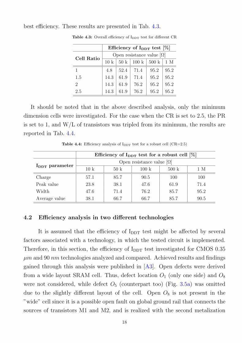
best efficiency. These results are presented in Tab. 4.3.
Table 4.3: Overall efficiency of IDDT test for different CR
Efficiency of IDDT test [%]
Cell RatioOpen resistance value [Ω]
10 k 50 k 100 k 500 k 1 M
1 4.8 52.4 71.4 95.2 95.2
1.5 14.3 61.9 71.4 95.2 95.2
2 14.3 61.9 76.2 95.2 95.2
2.5 14.3 61.9 76.2 95.2 95.2
It should be noted that in the above described analysis, only the minimum
dimension cells were investigated. For the case when the CR is set to 2.5, the PR
is set to 1, and W/L of transistors was tripled from its minimum, the results are
reported in Tab. 4.4.
Table 4.4: Efficiency analysis of IDDT test for a robust cell (CR=2.5)
Efficiency of IDDT test for a robust cell [%]
IDDT parameterOpen resistance value [Ω]
10 k 50 k 100 k 500 k 1 M
Charge 57.1 85.7 90.5 100 100
Peak value 23.8 38.1 47.6 61.9 71.4
Width 47.6 71.4 76.2 85.7 95.2
Average value 38.1 66.7 66.7 85.7 90.5
4.2 Efficiency analysis in two different technologies
It is assumed that the efficiency of IDDT test might be affected by several
factors associated with a technology, in which the tested circuit is implemented.
Therefore, in this section, the efficiency of IDDT test investigated for CMOS 0.35
µm and 90 nm technologies analyzed and compared. Achieved results and findings
gained through this analysis were published in [A3]. Open defects were derived
from a wide layout SRAM cell. Thus, defect location O1 (only one side) and O8
were not considered, while defect O5 (counterpart too) (Fig. 3.5a) was omitted
due to the slightly different layout of the cell. Open O8 is not present in the
”wide” cell since it is a possible open fault on global ground rail that connects the
sources of transistors M1 and M2, and is realized with the second metalization
18

layer. Another power rail related open fault is O1. In this way, 17 open faults
altogether were considered in this analysis. The designed circuit under test was a
synchronous 64-bit SRAM with parallel 8-bit input/output. The cell dimensions
were not kept on minimum, where the width of all transistors was nearly three
times greater than in 4.1 and the length was set to minimum.
In this analysis, five parameters of the IDDT waveform were evaluated. Except
for the peak time (the time moment when the IDDT waveform reaches its maxi-
mum), four other parameters are the same as in 4.1. The peak width was stated
in two ways. In the first case, it was stated in a relative way, where the width
value depends on the highest value of the waveform. Thus, the relative width was
measured on the current waveform at 10% of the peak value (Ilim in Fig. 1.2a).
In the second case, the width was measured at a constant value of Ilim.
As opposed to the analysis presented in section 4.1, here open faults were
modeled only using a resistor, and thus, for open faults from Group II (section
3.3) the parasitic capacitances were omitted. Then, MC analysis consisting of 100
runs on the fault-free circuit was performed and TBs for monitored parameters
were specified.
In Tab. 4.5, the overall efficiency of all IDDT parameters (in covering all 17
possible locations of open defects) is presented for 0.35 µm and 90 nm CMOS
technology, respectively. Check marks denote detected open faults, while X marks
denote undetected opens for each write direction and three different values of
open resistance. Open faults marked with apostrophe denote the counterparts of
symmetrical open faults.
4.3 The effect of sensor hardware on IDDT
In experiments presented in [A5] and [A6] a MOS transistor was used as a
sensing element in the test hardware. A PMOS transistor was connected between
the CUT and the power supply, while its gate was grounded. In this experiment,
the efficiency dependence of IDDT test and the CR and PR (where CR was set
as in section 4.1 and PR was in all cases set to 1) on the dimensions of the
sensing element was investigated. In the simulation setup, the CUT had the
same structure as the one designed in a 90 nm CMOS technology (presented in
19

Table 4.5: Overall IDDT test efficiency in 0.35 µm and 90 nm process
Open
resistance
Efficiency for 0.35 µm process Efficiency for 90 nm process
10 kΩ 100 kΩ 1 MΩ 10 kΩ 100 kΩ 1 MΩ
Writing Log0 Log1 Log0 Log1 Log0 Log1 Log0 Log1 Log0 Log1 Log0 Log1
O11 X X X X X X X X X X X X
O9 X X X X X X X X X X X X
O0 X X X X X X X X X X X X
O10 X X X X X X X X X X X X
O′1 X X X X X X X X X X X X
O3 X X X X X X X X X X X X
O2 X X X X X X X X X X X X
O′2 X X X X X X X X X X X X
O′3 X X X X X X X X X X X X
O4 X X X X X X X X X X X X
O′4 X X X X X X X X X X X X
O7 X X X X X X X X X X X X
O′7 X X X X X X X X X X X X
O′11 X X X X X X X X X X X X
O′9 X X X X X X X X X X X X
O6 X X X X X X X X X X X X
O′6 X X X X X X X X X X X X
Efficiency 41.2% 64.7% 88.2% 41.2% 70.6% 100%
section 4.2), where dimensions of the cells were kept as small as possible. For
a faulty cell, there were 23 locations considered (compared to section 4.1, opens
were considered in every possible node and were modeled with resistors). The
value of open resistance was set to 10 kΩ, 100 kΩ and 1 MΩ. The channel length
of the PMOS sensing transistor was set to minimum, while the width was set to 4
µm and 8 µm. The TB was gained by MC analysis of 100 runs. The test efficiency
was calculated from the dynamic current drawn by the sensing transistor. Test
efficiency is shown in Tab. 4.6 and Tab. 4.7.
Choosing a sensing element, however, is by far the smaller problem. On the
other hand, designing proper test hardware is a real challenge. In section 1, it
was already discussed that the processing of signals such as the IDDT current is
very difficult. Considering the analog characteristics of MOS transistors in deep
sub-micron technologies (e.g. 90 nm), the task seems very difficult. Though, the
presented results show that it is not always necessary to amplify the signal as it
is, since the peak value does not have the highest efficiency. The most efficient
parameter appears to be the charge carried by the IDDT waveform. However, this
20

Table 4.6: Efficiency of IDDT test for cell ratios 1 and 1.5 (a PMOS sensing element)
Efficiency of IDDT test for CR=1/1.5 [%]
IDDT parameterOpen resistance value [Ω]
PMOS width10 k 100 k 1 M
Charge 8.7/21.7 87/87 100/100
4 µmPeak value 8.7/13 56.5/52.2 69.6/73.9
Width 8.7/8.7 56.5/69.6 82.6/100
Average value 4.3/4.3 47.8/78.3 95.7/100
Charge 8.7/21.7 87/87 100/100
8 µmPeak value 4.3/13 39.1/52.2 65.2/73.9
Width 8.7/8.7 47.8/60.9 82.6/91.3
Average value 4.3/4.3 43.5/52.2 87/100
Table 4.7: Efficiency of IDDT test for cell ratios 2 and 2.5 (a PMOS sensing element)
Efficiency of IDDT test for CR=2/2.5 [%]
IDDT parameterOpen resistance value [Ω]
PMOS width10 k 100 k 1 M
Charge 39.1/39.1 73.9/87 100/100
4 µmPeak value 13/13 52.2/56.5 87/82.6
Width 34.8/26.1 65.2/73.9 100/100
Average value 8.7/8.7 69.6/82.6 100/100
Charge 30.4/39.1 87/87 100/100
8 µmPeak value 13/13 43.5/52.2 69.6/65.2
Width 8.7/17.4 69.6/78.3 95.7/100
Average value 8.7/8.7 60.9/73.9 91.3/95.7
charge is really low compared to technologies, where higher power supply voltages
and greater dimensions of transistors are used. Hence, a simple integration of
the current waveform could not be successful. Experimental design of sensor for
dynamic supply current monitoring was presented in [A5, A6, A8].
The proposed sensor circuit is depicted in Fig. 4.1. Firstly, the sensing element
(denoted as M1) is chosen, where several factors have to be taken into account.
One important factor is the increased leakage current in deep sub-micron tech-
nologies, which in the form of static current might create a significant voltage
drop across the sensing element. The consequence of the voltage drop is the re-
duced supply voltage level for the CUT (SRAM array presented at the beginning
of section 4.3. Therefore, the dimensions of the sensing element (representing a
21

resistance) should be chosen so that it does not exceed a certain voltage drop,
which for instance, in the case of a 1.2 V power supply with 10% tolerance is 120
mV.
CUT
Vout
M1 M2
M3
M13
Vsense C1
M12
M19
M18
M16
M17C2
+
-
Integration and
amplification
Vhalf1Vhalf2
Input
circ
uit
Outp
ut
circ
uit
V amp
Zout
Zin
Figure 4.1: Current monitor block schematic
Two experiments were made on the test setup with the current monitor from
Fig. 4.1. In the first experiment, the leakage current consumption of the SRAM
array was neglected, thus, creating no voltage drop on the sensing element. In the
second experiment, the leakage current was set to 200 µA. The leakage current was
modeled using an ideal current source, which was connected between the drain
of the sensing transistor and ground creating a voltage drop of approximately
100 mV. In both cases, the sensing element with the channel width of 4 µm and
the minimum length was used and the CR was set 2.5 and PR to 1. In each
case different threshold values were used. This was done due to the fact that the
additional voltage drop across the sensing element decreases the supply voltage of
SRAM cells, which causes lower IDDT current levels and hence, a lower dynamic
voltage drop. The achieved efficiency and its comparison to the efficiency of the
most efficient parameter of I textsubscriptDDT current (the charge carried by the
waveform or the integral of the waveform) are shown in Tab. 4.8.
The presented current monitor is just an experimental circuit, which demon-
strates that even in a deep sub-micron technology it is possible to deal with the
IDDT current.
22

Table 4.8: Efficiency of the IDDT current monitor
Efficiency in [%]
ParameterOpen resistance value [Ω]
10 k 100 k 1 M
IDDT charge 39 87 100
Vout peak (no leakage) 8 60 100
Vhalf2 peak (no leakage) 17 78 100
Vout peak (with leakage) 0 60 100
Vhalf2 peak (with leakage) 21 87 100
4.4 The effect of parasitics and leakage current on IDDT
In the above discussed experiments, parasitic components of the power dis-
tributing and control circuitry metalization were neglected. In reality, each wire
represents a resistance and a parasitic capacitance, where they can be modeled
using an RC component. The IDDT current flows through these wires and due to
the parasitics it changes its shape. The cell that is the closest to the power supply
will have a different shape as the one that is the farthest. Also the current drawn
by the last cell will be different when measured at a given cell and the power sup-
ply source. The change of the IDDT current of the last cell is measured in several
nodes along the current path, as depicted in Fig. 4.2a. A different charge drawn
from the first cell and from the last cell is expected due to the degraded supply
voltage level caused by the parasitic resistance of the supply rail especially, if an
increased value of quiescent current is considered due to leakage currents.
A SRAM block of 4096 bits (512 one byte words) designed in a 90 nm CMOS
technology was used as the CUT in this experiment. CR and PR were set to 2.5
and 1, respectively. The faulty cells were modeled as discussed in section 3.3 and
hence, the number of opens was also identical. All parameters were calculated
at Ilim = 2 µA (+ leakage current value). The schematic used is depicted in
Fig. 4.2b. It consists of 4096 SRAM cells and ”AND” logic gates, which were
used on the input of BLs(nBLs) and WLs in order to clock the input signals.
Simulations were carried out with taking into account the effect of leakage
current mechanisms on IDDT. The value of leakage current in active state (read or
write) was set to 0.3 µA, and in idle state the value was set to 0.32 µA [17]. The
23

125.0 125.1 125.2 125.3 125.4 125.5
-5
0
5
10
15
20
Current at the cell...
Current at the supply
I DDT[µA]
Time [ns]
Fromsupplytocell
(a) IDDT current of the last cell measured at different
positions
BL BLWL
BL BLWL
BL BLWL
CLK1
CLK1
WL0
WL1
CLK2CLK2 CLK2 CLK2D0
nD0
D1
nD1
VDD
(b) SRAM array used as the CUT
Figure 4.2: Current and CUT
leakage current is modeled with a DC current source connected between the source
of pull-up transistors and ground. In Tab. 4.9, Tab. 4.10 and Tab. 4.11, parameters
without the leakage current considered and parameters of IDDT current affected
by the leakage current are presented before and after the slash, respectively.
The “obvious” IDDT test approach
In the efficiency analysis of IDDT test, two cells of the SRAM array from Fig. 4.2b
were investigated: Cell1 (the first bit in the first byte) that is the closest to the
supply rail and Cell4096 (the last bit in the last byte) that is the farthest from
the supply rail, since these two cells have the greatest difference in their parasitic
components. On these cells five operations were performed altogether: a common
write of Log1 to both investigated cells, then the sequential write of Log0 and
Log1 to Cell1, and finally, the sequential write of Log0 and Log1 to Cell4096.
TBs are set based upon MC analysis, where both the process variation and
mismatch are considered. However, the TB for the first cell is different from that
of the last cell. For this purpose, the smallest of the lower limit and the greatest
of the higher limit of these two TBs were used, creating a union of the above
mentioned two TBs. In practice, this is the fastest way to distinguish between
a faulty circuit and the fault-free one by this approach. The overall efficiency of
the obvious IDDT approach (performed by two transition write processes in every
24
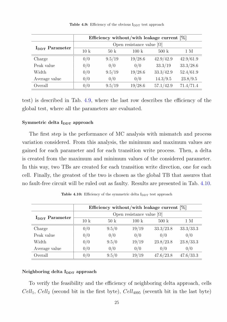
Table 4.9: Efficiency of the obvious IDDT test approach
Efficiency without/with leakage current [%]
IDDT ParameterOpen resistance value [Ω]
10 k 50 k 100 k 500 k 1 M
Charge 0/0 9.5/19 19/28.6 42.9/42.9 42.9/61.9
Peak value 0/0 0/0 0/0 33.3/19 33.3/28.6
Width 0/0 9.5/19 19/28.6 33.3/42.9 52.4/61.9
Average value 0/0 0/0 0/0 14.3/9.5 23.8/9.5
Overall 0/0 9.5/19 19/28.6 57.1/42.9 71.4/71.4
test) is described in Tab. 4.9, where the last row describes the efficiency of the
global test, where all the parameters are evaluated.
Symmetric delta IDDT approach
The first step is the performance of MC analysis with mismatch and process
variation considered. From this analysis, the minimum and maximum values are
gained for each parameter and for each transition write process. Then, a delta
is created from the maximum and minimum values of the considered parameter.
In this way, two TBs are created for each transition write direction, one for each
cell. Finally, the greatest of the two is chosen as the global TB that assures that
no fault-free circuit will be ruled out as faulty. Results are presented in Tab. 4.10.
Table 4.10: Efficiency of the symmetric delta IDDT test approach
Efficiency without/with leakage current [%]
IDDT ParameterOpen resistance value [Ω]
10 k 50 k 100 k 500 k 1 M
Charge 0/0 9.5/0 19/19 33.3/23.8 33.3/33.3
Peak value 0/0 0/0 0/0 0/0 0/0
Width 0/0 9.5/0 19/19 23.8/23.8 23.8/33.3
Average value 0/0 0/0 0/0 0/0 0/0
Overall 0/0 9.5/0 19/19 47.6/23.8 47.6/33.3
Neighboring delta IDDT approach
To verify the feasibility and the efficiency of neighboring delta approach, cells
Cell1, Cell2 (second bit in the first byte), Cell4095 (seventh bit in the last byte)
25

and Cell4096 were investigated. The following operations were performed on these
cells: a common write of Log1 to all four cells, then the sequential write of Log0
and Log1 to Cell1, and then the same sequence to all the remaining cells.
Firstly, MC analysis with mismatch but with no process variation considered
is performed. This is possible due to the fact that neighboring cells will have
the same process variation with high probability. In this way, the maximum
and the minimum values are obtained for each IDDT parameter for cells Cell1,
Cell2, Cell4095 and Cell4096. This approach relies on the subtraction of given IDDT
parameter values of two neighboring cells. The TB used in testing Cell1 is set
by subtracting the smallest value of the monitored parameter from the greatest
value of the same parameter of Cell1 and Cell2, gained by MC analysis. Then, a
TB for the last two cells (Cell4095 and Cell4096) is gained in the same way. Thus,
there are two TBs for each write direction and the greatest one is chosen for each
write direction. In Tab. 4.11, the efficiency of the neighboring delta approach is
presented, with the last row representing the overall efficiency (all parameters of
IDDT are evaluated).
Table 4.11: Neighboring delta approach efficiency (for one global TB used)
Efficiency without/with leakage current [%]
IDDT ParameterOpen resistance value [Ω]
10 k 50 k 100 k 500 k 1 M
Charge 4.8/0 61.9/28.6 66.7/38.1 85.7/52.4 85.7/57.1
Peak value 0/0 9.5/9.5 33.3/19 52.4/47.6 52.4/47.6
Width 0/0 38.1/28.6 47.6/38.1 57.1/52.4 57.1/57.1
Average value 0/0 14.3/19 42.9/38.1 52.4/38.1 52.4/38.1
Overall 4.8/0 61.9/28.6 66.7/38.1 85.7/57.1 85.7/38.1
The progressive TB is a tolerance band, where on a theoretical level each cell
has its own TB. Of course, to create such TBs for high capacity memory with MC
analysis is very time consuming. Instead, some assumptions have to be made.
In a fault-free circuit, dynamic current parameter values can be assigned to each
cell, and based on their distance from the power supply they can be put in order,
where some parameters are going to rise with distance (the peak width) and some
are going to decrease (for instance the peak value). Either way, the distance of
26
a cell from the power supply (the cell number) is the parameter of the function.
In the same MC analysis, it is then expected that the TBs are going to follow a
similar manner as the given parameter. For example, the charge value is going
to decrease with the distance from the power supply, while the TB for the same
parameter is going to rise with distance. In Tab. 4.12, results achieved for such a
theoretical case are presented. It can be seen that the efficiency of the charge of
the IDDT waveform has increased, which would mean that the delta approach is
the most efficient approach.
Table 4.12: Neighboring delta approach efficiency vs. obvious approach (progressive TB)
Efficiency without/with leakage current [%]
IDDT ParameterOpen resistance value [Ω]
10 k 50 k 100 k 500 k 1 M
Charge 4.8/0 28.6/33.3 38.1/42.9 61.9/61.9 76.2/81
Obvio
us
Peak value 4.8/4.8 23.8/14.3 42.9/42.9 52.4/52.4 42.9/52.4
Width 0/0 33.3/33.3 42.9/42.9 42.9/61.9 71.4/81
Average value 0/4.8 0/23.8 19/42.9 52.4/81 52.4/81
Charge 4.8/4.8 61.9/61.9 66.7/66.7 85.7/76.2 95.2/95.2
Neig
hb
ori
ng
Peak value 4.8/4.8 9.5/61.9 61.9/52.4 71.4/71.4 71.4/71.4
Width 4.8/4.8 61.9/61.9 66.7/66.7 76.2/76.2 95.2/95.2
Average value 4.8/14.3 61.9/61.9 61.9/61.9 85.7/85.7 85.7/85.7
Some opens might remain hidden also for the resistance value of 1 MΩ. For
instance, O7 and O8 remained hidden for all tests in our experiment. For the
obvious approach, typically O7, O8 and O9 remained hidden in the leakage-free
and leakage-affected circuits. In the case of the symmetric delta approach, the
hidden defects were O1, O3, O6, O7, O8 and O9, and for the neighboring delta
approach, opens O7 and O8 remained uncovered. These results in comparison to
results presented earlier in sections 4.1 and 4.2, where no parasitic components and
the same/similar open defects were considered, show that leakage and parasitics
have a huge impact on the efficiency of IDDT test.
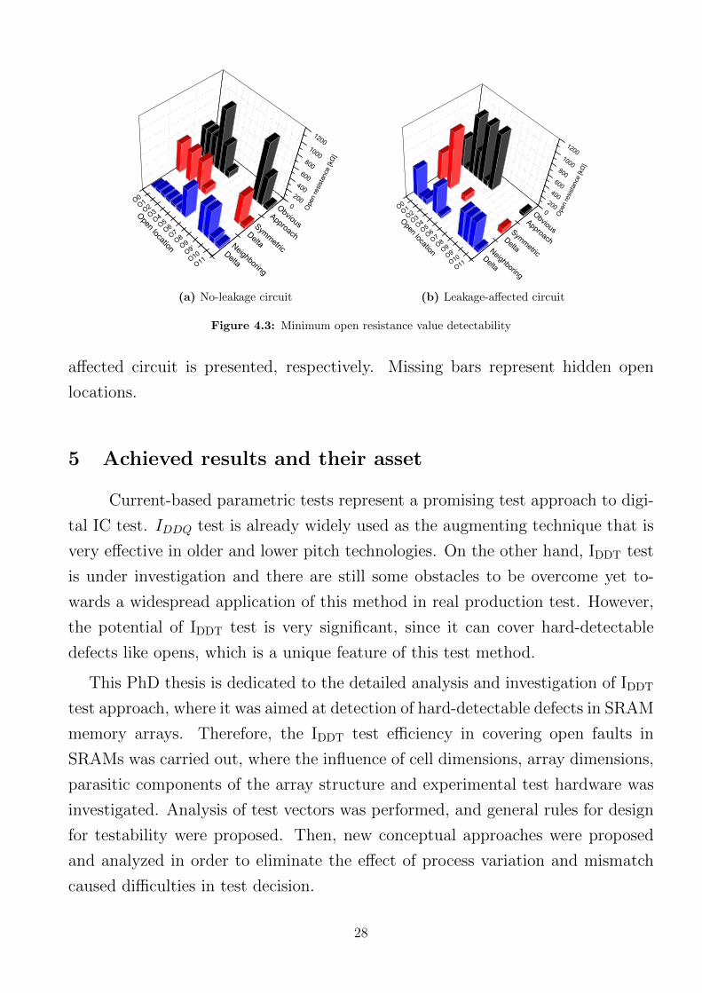
Fig. 4.3 shows the minimum value of the open resistance, from which an open
defect was detected for each IDDT test approach, when all parameters of the IDDT
current were considered. In Fig. 4.3a and Fig. 4.3b, the minimum open resistance
value detectability achieved in the leakage-free SRAM array and the leakage-
27
O0O1
O2O3
O4O5
O6O7
O8O9
O9’
O10
O11
0
200
400
600
800
1000
1200
Neighboring
Delta
Open
location
Ope
nre
sist
ance
[kΩ
]
ObviousApproach
Symmetric
Delta
(a) No-leakage circuit
O0O1
O2O3
O4O5
O6O7
O8O9
O9’
O10
O11
0
200
400
600
800
1000
1200
Neighboring
Delta
Open
location
Ope
nre
sist
ance
[kΩ
]
ObviousApproach
Symmetric
Delta
(b) Leakage-affected circuit
Figure 4.3: Minimum open resistance value detectability
affected circuit is presented, respectively. Missing bars represent hidden open
locations.
5 Achieved results and their asset
Current-based parametric tests represent a promising test approach to digi-
tal IC test. IDDQ test is already widely used as the augmenting technique that is
very effective in older and lower pitch technologies. On the other hand, IDDT test
is under investigation and there are still some obstacles to be overcome yet to-
wards a widespread application of this method in real production test. However,
the potential of IDDT test is very significant, since it can cover hard-detectable
defects like opens, which is a unique feature of this test method.
This PhD thesis is dedicated to the detailed analysis and investigation of IDDT
test approach, where it was aimed at detection of hard-detectable defects in SRAM
memory arrays. Therefore, the IDDT test efficiency in covering open faults in
SRAMs was carried out, where the influence of cell dimensions, array dimensions,
parasitic components of the array structure and experimental test hardware was
investigated. Analysis of test vectors was performed, and general rules for design
for testability were proposed. Then, new conceptual approaches were proposed
and analyzed in order to eliminate the effect of process variation and mismatch
caused difficulties in test decision.
28
The main contributions of this thesis to the related field of science are the
following:
• The important contribution of this work is the extensive analysis of IDDT test
efficiency in covering weak open faults in SRAM arrays, where its depen-
dence on the cell ratio, cell dimensions, test hardware, leakage current and
finally, the parasitic components of a realistic SRAM array was investigated.
The test efficiency was based on the monitoring of four main parameters of
the dynamic supply current waveform, which were the integral of the wave-
form (charge), the highest value of the waveform (peak value), the width
of the waveform (a time interval), and the average value of the waveform.
As an essential outcome of this analysis, the most efficient parameters were
identified.
• From the fault modeling point of view, the performed extraction of open
defects from the SRAM cell layout is another very relevant asset. The open
defects were classified in three groups, based on their location in the cell.
The proposed open fault classification brings more realistic fault model of
opens.
• In order to reduce the test length, an investigation of tests towards the min-
imum test length setting was performed. Moreover, the possibility of attach-
ing an extra IDDT test to well known march memory tests was investigated,
where the march test patterns important for IDDT test were highlighted. Such
an attachment would greatly benefit the test time and test complexity, since
no change to applied tests is required.
• A set of general rules to design for IDDT testability was proposed that is
beneficial for future research and application of IDDT test based on monitoring
of the most efficient IDDT parameters.
• The major contribution that is important mainly from the future research
point of view, is a new conceptual delta IDDT test approach (especially, the
neighboring delta approach), which was developed in order to eliminate the
undesired effect of process variation and parasitic components of routing
wires, representing a great problem in deep sub-micron technologies. This
29
conceptual approach to IDDT test might significantly increase the IDDT test
efficiency.
• An important practical contribution of this thesis is design of an experi-
mental IDDT measurement hardware in a deep sub-micron technology, which
proves that despite the described difficulties, it is still possible to derive an
analog output proportional to the IDDT current and achieve satisfactory high
efficiency in covering open faults.
6 Conclusion
The high scale of integration, increasing complexity and incessant technol-
ogy scaling introduce new challenges for IC test engineers in terms of new failure
mechanisms and IC reliability. A very actual problem of such advanced technolo-
gies is the high density of open defects, which are considered to be hard-detectable
defects. Since functional test and other digital tests are not very efficient in cov-
ering open defects, new augmenting test methods are required. Theoretically, the
only known method being very effective here is IDDT test, however, the physical
implementation of this approach in real IC testing represents a great challenge.
That was also the major motivation for our research and the main reason why
the investigation of IDDT test approach was chosen as the subject of this PhD
thesis. In this work, a comprehensive investigation of the IDDT test efficiency in
covering weak open defects was done. The efficiency was investigated on simple
structures as one SRAM cell, a more complex 64-bit SRAM array and a 512-byte
SRAM array with parasitic components of interconnecting wires considered. The
achieved efficiency is based on several parameters of the IDDT waveform, where
the charge carried by the waveform appeared to be the most efficient parame-
ter. Moreover, in this work, possible march test solutions were investigated, and
considerations about the design for testability were made. A new conceptual
approach to IDDT test implementation – the delta IDDT approach was proposed,
which by choosing the right decision criteria could further enhance the the overall
efficiency of this current-based test.
30
From the experiments performed on SRAM arrays, it could be derived that
the IDDT test efficiency depends on several factors such as the cell dimensions and
SRAM array complexity. Another important outcome is that the real efficiency
(compared to the ideal, theoretical results) is reduced when parasitic components
like leakage current and RC components of wires are considered. Despite the
reduced efficiency, the results show that IDDT test is a potential solution for de-
tecting weak open defects with the value of the open resistance around 1 MΩ.
Though, the realization of test hardware is still a challenge, especially in deep
sub-micron technologies.
Our future research will be focused on the development of scalable hybrid mea-
surement hardware for IDDT test based on the monitoring of the charge carried by
the IDDT current. Also another conceptual approach is targeted, where the deci-
sion criteria is based on the particular CUT, in which only the effect of mismatch
is considered to be critical. The whole concept shall be tested on an experimental
integrated circuit.
31
Author’s publications
Current Contents journals:
[A11] G. Gyepes, V. Stopjakova, D. Arbet, L. Majer, and J. Brenkus. A new IDDT test approach and
its efficiency in covering resistive opens in SRAM arrays. Microprocessors and Microsystems (2014),
DOI: http://dx.doi.org/10.1016/j.micpro.2014.04.006.
[A20] D. Arbet, V. Stopjakova, L. Majer, G. Gyepes, and G. Nagy. New obist using on-chip compensation
of process variations toward increasing fault detectability in analog ICs. Nanotechnology, IEEE
Transactions on, 12(4):486–497, 2013.
[A23] D. Arbet, V. Stopjakova, J. Brenkus, G. Gyepes, M. Kovac, and L. Majer. BIST architecture for
oscillation test of analog ICs and investigation of test hardware influence. Microelectronics Reliability,
DOI: http://dx.doi.org/10.1016/j.microrel.2013.12.027, 2014.
International scientific journals:
[A16] D. Arbet and V. Stopjakova and J. Brenkus and G. Gyepes. On-chip Parametric Test of R-2R
Ladder Digital-to-Analog Converter and Its Efficiency. International Journal of Microelectronics and
Computer Science, Vol. 3, nr 2:73–80, 2012.
International conferences (Scopus and Web of Science):
[A3] G. Gyepes, J. Brenkus, D. Arbet, and V. Stopjakova. Comparison of iddt test efficiency in covering
opens in srams realised in two different technologies. In Design and Diagnostics of Electronic Circuits
Systems (DDECS), 2011 IEEE 14th International Symposium on, pages 395–396, 2011.
[A5] G. Gyepes, D. Arbet, J. Brenkus, and V. Stopjakova. Application of iddt test towards increasing
sram reliability in nanometer technologies. In Design and Diagnostics of Electronic Circuits Systems
(DDECS), 2012 IEEE 15th International Symposium on, pages 167–170, 2012.
[A6] G. Gyepes, D. Arbet, L. Majer, and V. Stopjakova. An on-chip iddt current sensor based on current-
to-voltage conversion. In Applied Electronics (AE), 2012 International Conference on, pages 87–90,
2012.
[A8] G. Gyepes, D. Arbet, J. Brenkus, V. Stopjakova, and J. Mihalov. An on-chip dynamic supply
current monitor for testing of digital circuits. In Radioelektronika (RADIOELEKTRONIKA), 2013
23rd International Conference, pages 156–161, 2013.
[A10] G. Gyepes, V. Stopjakova, D. Arbet, G. Nagy and L. Majer. A robust multipurpose PLL with lock
detector designed in a 0.35 um CMOS technology. In Applied Electronics (AE), 2013 International
Conference on, pages 85–88, 2013.
32

[A13] D. Arbet, J. Brenkus, G. Gyepes, and V. Stopjakova. Increasing the efficiency of analog obist
using on-chip compensation of technology variations. In Design and Diagnostics of Electronic Circuits
Systems (DDECS), 2011 IEEE 14th International Symposium on, pages 71–74, 2011.
[A14] D. Arbet, G. Gyepes, J. Brenkus, and V. Stopjakova. Obist strategy versus parametric test
- efficiency in covering catastrophic faults in active analog filters. In Design and Diagnostics of
Electronic Circuits Systems (DDECS), 2012 IEEE 15th International Symposium on, pages 193–194,
2012.
[A15] D. Arbet, G. Gyepes, J. Brenkus, V. Stopjakova, and J. Mihalov. On-chip parametric test of
binary-weighted r-2r ladder d/a converter and its efficiency. In Mixed Design of Integrated Circuits
and Systems (MIXDES), 2012 Proceedings of the 19th International Conference, pages 441–446, 2012.
[A17] D. Arbet, G. Nagy, G. Gyepes, and V. Stopjakova. Design of rail-to-rail operational amplifier with
offset cancelation in 90nm technology. In Applied Electronics (AE), 2012 International Conference
on, pages 17–20, 2012.
[A18] D. Arbet, G. Nagy, V. Stopjakova, and G. Gyepes. Efficiency of oscillation-based bist in 90nm
cmos active analog filters. In Design and Diagnostics of Electronic Circuits Systems (DDECS), 2013
IEEE 16th International Symposium on, pages 263–266, 2013.
[A19] J. Brenkus, V. Stopjakova, and G. Gyepes. Numerical method for dc fault analysis simplification
and simulation time reduction. In Design and Diagnostics of Electronic Circuits Systems (DDECS),
2013 IEEE 16th International Symposium on, pages 170–174, 2013.
[A21] V. Stopjakova, G. Nagy, D. Arbet, L. Majer and G. Gyepes. Low-power readout IC with high
dynamic range for MCM-based noise dosimeter. In Applied Electronics (AE), 2013 International
Conference on, pages 275–278, 2013.
[A22] L. Majer, J. Mihalov, V. Stopjakova, J. Brenkus, G. Gyepes and M. Uram. Multi-communication
wireless system for smart households. In Telecommunications Forum (TELFOR), 2013 21st, pages
272–275, 2013.
[A25] Brenkus, J. and Stopjakova, V. and Arbet, D. and Gyepes, G. and Majer, L. A novel impedance
calculation method and its time efficiency evaluation. In Design and Diagnostics of Electronic Circuits
Systems (DDECS), 2014 IEEE 17th International Symposium on, pages 99–103, 2014.
[A26] Arbet, D. and Nagy, G. and Stopjakova, V. and Gyepes, G. A Self-Calibrated Binary Weighted
DAC in 90nm CMOS Technology. In International Conference on Microelectronics (MIEL 2014),
accepted for publication, 2014.
33

Other conferences:
[A2] G. Gyepes and V. Stopjakova. Efficiency of dynamic supply current testing in detecting open
defects and gate oxide shorts in static ram cells. In Pocıtacove architektury a diagnostika 2010,
Cesko-slovensky seminar pro studenty doktorskeho studia., page 27–32, 2010.
[A7] G. Gyepes and V. Stopjakova. Application of iDDT test in sram arrays towards efficient detection
of weak opens. In Pocıtacove architektury a diagnostika 2010, Cesko-slovensky seminar pro studenty
doktorskeho studia., page 139–144, 2012.
[A12] J. Mihalov, V. Stopjakova, L. Nagy, G. Gyepes and D. Arbet. Investigation of 4th Order Loop
Filter Bahavior with the First Discrete Time Integrator. In AIM 2009. International Symposium on
Advances in Mechatronics, pages 30–37, 2009.
[A1] G. Gyepes and V. Stopjakova. Efficiency of dynamic supply current testing in detecting open defects
in static ram cells. In Elitech ’10, 2010 12th Conference of Doctoral Students, 2010.
[A4] G. Gyepes and V. Stopjakova. Application of iDDT test towards increasing sram reliability in
nanometer technologies. In Pocıtacove architektury a diagnostika 2010, Cesko-slovensky seminar pro
studenty doktorskeho studia., page 91–96, 2011.
[A9] G. Gyepes, V. Stopjakova, D. Arbet, J. Mihalov, and L. Majer. Built-in test for srams using dynamic
supply current monitoring. In Proceedings of ADEPT, 1st International Conference on Advances in
Electronic and Photonic Technologies, pages 177–180, 2013.
[A24] Brenkus, J. and Stopjakova, V. and Arbet, D. and Gyepes, G. and Majer, L. Impedance Calcu-
lation Methodology for Fault Simulation of Analog and Mixed-signal Circuits. In Radioelektronika
(RADIOELEKTRONIKA), 2014 24rd International Conference, 4 pages, 2014.
34

References
(Number of references in PhD Thesis: 108)
[1] Sachdev, Manoj and Gyvez, Jose Pineda de, Defect-Oriented Testing for Nano-Metric CMOS VLSI
Circuits (Frontiers in Electronic Testing). Secaucus, NJ, USA: Springer-Verlag New York, Inc.,
2007.
[2] Alorda, B. and Rosales, M. and Soden, J. and Hawkins, C. and Segura, J., “Charge based tran-
sient current testing (CBT) for submicron CMOS SRAMs,” in Test Conference, 2002. Proceedings.
International, pp. 947–953, 2002.
[3] Pavlov, Andrei and Sachdev, Manoj, CMOS SRAM Circuit Design and Parametric Test in Nano-
Scaled Technologies: Process-Aware SRAM Design and Test. Springer Publishing Company, Incor-
porated, 1st ed., 2008.
[4] Soden, Jerry M. and Hawkins, Charles F. and Gulati, Ravi K. and Mao, Weiwei, “IDDQ testing: A
review.,” J. Electronic Testing, vol. 3, pp. 291–303, 1992.
[5] Frenzel, J. F. and Marinos, P. N., “Power Supply Current Signature (PSCS) Analysis: A New
Approach to System Testing,” in Test Conference, 1987. Proceedings., International, pp. 125–135,
1987.
[6] Guibane, B. and Hamdi, B., “DFT for analog and mixed signal IC based on IDDQ scanning,” in
Mixed Design of Integrated Circuits and Systems (MIXDES), 2012 Proceedings of the 19th Interna-
tional Conference, pp. 431–435, 2012.
[7] Caravella, J.S. and Mietus, D.F. and Quigley, J.H., “Circuit techniques for standby mode/Iddq test
compatible voltage comparators,” in ASIC Conference and Exhibit, 1995., Proceedings of the Eighth
Annual IEEE International, pp. 216–217, 1995.
[8] Burns, M. and Roberts, G., W., An introduction to mixed-signal IC test and measurement. Oxford
University Press, USA, 2000.
[9] Gizopoulos, Dimitris, Advances in Electronic Testing: Challenges and Methodologies). Springer-
Verlag New York, Inc., 2006.
[10] Plusquellic, J.F. and Chiarulli, D.M. and Levitan, S.P., “Digital integrated circuit testing using
transient signal analysis,” in Test Conference, 1996. Proceedings., International, pp. 481–490, 1996.
[11] Jian Liu and Makki, R.Z. and Kayssi, A., “Dynamic power supply current testing of CMOS SRAMs,”
in Test Symposium, 1998. ATS ’98. Proceedings. Seventh Asian, pp. 348–353, 1998.
[12] Jiang Shuyan and Chen Guangju and Xuan, Xie, “A Research on IDDT Test Pattern Generation
Algorithm Based on Digragh Model,” in Communications, Circuits and Systems, 2007. ICCCAS
2007. International Conference on, pp. 1189–1192, 2007.
35

[13] Yoon, D-H and Kim, H-S and Kang, S., “Dynamic power supply current testing for open defects in
CMOS SRAMs,” ETRI Journal, vol. 23, pp. 77–84, 2001.
[14] Makki, R.Z. and Shyang-Tai Su and Nagle, T., “Transient power supply current testing of digital
CMOS circuits,” in Test Conference, 1995. Proceedings., International, pp. 892–901, 1995.
[15] Arumi, D. and Rodriguez-Montaes, R. and Figueras, J., “Experimental Characterization of CMOS
Interconnect Open Defects,” Computer-Aided Design of Integrated Circuits and Systems, IEEE
Transactions on, vol. 27, no. 1, pp. 123–136, 2008.
[16] Montanes, R.R. and de Gyvez, J.P. and Volf, P., “Resistance characterization for weak open defects,”
Design Test of Computers, IEEE, vol. 19, no. 5, pp. 18–26, 2002.
[17] Feng Zhang and Ge Zhang and Yi Yang and Jun Wang, “An Effective Approach For Subtreshold And
Gate Leakage Power Estimation Of SRAM,” in Integrated Circuits, 2007. ISIC ’07. International
Symposium on, pp. 325–328, 2007.
36