application of seven level multi inverter to photo voltaic ... · application of seven level multi...
TRANSCRIPT
Page 465
Application of Seven Level Multi Inverter to Photo Voltaic System
Ganesh Ashok Ubale
M.Tech (Digital Systems) ETC,
Government College of Engineering,
Jalgaon (Maharastra).
Prof.S.O.Dahad, M.Tech
HOD, ETC,
Government College of Engineering,
Jalgaon (Maharastra).
ABSTRACT:
A new solar power generation system, which is
composed of a dc/dc power converter and a new
seven-level inverter. The dc/dc power converter
integrates a dc–dc boost converter and a transformer to
convert the output voltage of the solar cell array into
two independent voltage sources with multiple
relationships. This new seven-level inverter is
configured using a capacitor selection circuit and a
full-bridge power converter, connected in cascade. The
capacitor selection circuit converts the two output
voltage sources of dc–dc power converter into a three-
level dc voltage, and the full-bridge power converter
further converts this three-level dc voltage into a
seven-level ac voltage. In this way, the proposed solar
power generation system generates a sinusoidal output
current that is in phase with the utility voltage and is
fed into the utility. The salient features of the proposed
seven-level inverter are that only six power electronic
switches are used, and only one power electronic
switch is switched at high frequency at any time. A
prototype is developed and tested to verify the
performance of this proposed solar power generation
system.
Exciting concept:
Conventional multilevel inverter topologies include the
diodeclamped, the flying-capacitor, and the cascade H-
bridge types. Diode-clamped and flyingcapacitor
multilevel inverters use capacitors to develop several
voltage levels. But it is difficult to regulate the voltage
of these capacitors. Since it is difficult to create an
asymmetric voltage technology in both the diode-
clamped and the flyingcapacitor topologies, the power
circuit is complicated by the increase in the voltage
levels that is necessary for a multilevel inverter.
For a single-phase seven-level inverter, 12 power
electronic switches are required in both the diode-
clamped and the flying-capacitor topologies.
Asymmetric voltage technology is used in the cascade
H-bridge multilevel inverter to allow more levels of
output voltage [17], so the cascade H-bridge multilevel
inverter is suitable for applications with increased
voltage levels. Two H-bridge inverters with a dc bus
voltage of multiple relationships can be connected in
cascade to produce a singlephase seven-level inverter
and eight power electronic switches are used. More
recently, various novel topologies for sevenlevel
inverters have been proposed. For example, a single-
phase seven-level grid-connected inverter has been
developed for a photovoltaic system [18]. This seven-
level grid-connected inverter contains six power
electronic switches. However, three dc capacitors are
used to construct the three voltage levels, which results
in that balancing the voltages of the capacitors is more
complex.
Proposed concept:
Multi-level inverter converter, configured by a level
generation part and a polarity generation part, is
proposed. There, only power electronic switches of the
level generation part switch in high frequency.
Amodular multilevel inverter with a new modulation
method is applied to the photovoltaic grid-connected
generator. The modular multilevel inverter is similar to
the cascade H-bridge type. For this, a new modulation
method is proposed to achieve dynamic capacitor
voltage balance. Overcome the problem of partial
shading of individual photovoltaic sources that are
connected in series. The dc bus of a full-bridge
inverter is configured by several individual dc blocks,
where each dc block is composed of a solar cell, a

Page 466
power electronic switch, and a diode. Controlling the
power electronics of the dc blocks will result in a
multilevel dc-link voltage to supply a full-bridge
inverter and to simultaneously overcome the problems
of partial shading of individual photovoltaic sources
Introduction:
The use of fuels has resulted in the global problem of
greenhouse effect. As the supplies of fuels are depleted
in the future, they will become increasingly expensive.
Since solar energy is becoming more important since it
produces less pollution and the cost of fossil fuel
energy is rising, while the cost of solar arrays is
decreasing. In particular, small-capacity distributed
power generation systems using solar energy may be
widely used in residential applications in the near
future. The power conversion interface is important to
grid connected solar power generation systems
because it converts the dc power generated by a solar
cell array into ac power and feeds this ac power into
the utility grid. An inverter is necessary in the power
conversion interface to convert the dc power to ac
power. Since the output voltage of a solar cell array is
low, a dc–dc power converter is used in a small-
capacity solar power generation system to boost the
output voltage, so it can match the dc bus voltage of
the inverter.
The power conversion efficiency of the power
conversion interface is important to insure that there is
no waste of the energy generated by the solar cell
array. The active devices and passive devices in the
inverter produce a power loss. The power losses due to
active devices include both conduction losses and
switching losses. Conduction loss results from the use
of active devices, while the switching loss is
proportional to the voltage and the current changes for
each switching and switching frequency. A filter
inductor is used to process the switching harmonics of
an inverter, so the power loss is proportional to the
amount of switching harmonics. The voltage change in
each switching operation for a multilevel inverter is
reduced in order to improve its power conversion
efficiency and the switching stress of the active
devices. The amount of switching harmonics is also
attenuated, so the power loss caused by the filter
inductor is also reduced.
PROPOSED CONCEPT CONFIGURATION:
Fig. 1.Configuration of the proposed solar power
generation system.
Above figure shows the configuration of the proposed
solar power generation system. The proposed solar
power generation system is composed of a solar cell
array, a dc–dc power converter, and a new seven-level
inverter. The solar cell array is connected to the dc–dc
power converter. The dc–dc power converter converts
the output power of the solar cell array into two
independent voltage sources with multiple
relationships, which are supplied to the seven-level
inverter.
The full-bridge power converter further converts this
three-level dc voltage to a seven-level ac voltage that
is synchronized with the utility voltage. In this way,
the proposed solar power generation system generates
a sinusoidal output current that is in phase with the
utility voltage and is fed into the utility, which
produces a unity power factor. As can be seen, this
new seven-level inverter contains only six power
electronic switches, so the power circuit is simplified.
POWER CONVERTER:
DC-DC type power converter:
The DC–DC power converter incorporates a boost
converter and a current-fed forward converter. The
boost converter is composed of an inductor LD, a
power electronic switch SD1, and a diode, DD3. The
boost converter charges capacitor C2 of the seven-

Page 467
level inverter. The current-fed forward converter is
composed of an inductor LD, power electronic
switches SD1 and SD2, a transformer, and diodes DD1
and DD2 . The current-fed forward converter charges
capacitor C1 of the seven-level inverter. The inductor
LD and the power electronic switch SD1 of the
current-fed forward converter are also used in the
boost converter. Fig. 2(a) shows the operating circuit
of the dc–dc power converter when SD1 is turned ON.
The solar cell array supplies energy to the inductor LD
. When SD1 is turned OFF and SD2 is turned ON, its
operating circuit is shown in Fig. 2(b). Accordingly,
capacitor C1 is connected to capacitor C2 in parallel
through the transformer, so the energy of inductor LD
and the solar cell array charge capacitor C2 through
DD3 and charge capacitor C1 through the transformer
and DD1 during the offstate of SD1. The boost
converter is operated in the continuous conduction
mode (CCM). The voltage of C2 can be represented as
Fig.2. Operation of dc–dc power converter: (a) SD
1 is on and (b) SD 1 is off.
WORKING PRINCIPLE:
SEVEN-LEVEL INVERTER:
As seen in Fig. 1, the seven-level inverter is composed
of a capacitor selection circuit and a full-bridge power
converter, which are connected in cascade. The
operation of the seven level inverter can be divided
into the positive half cycle and the negative half cycle
of the utility. For ease of analysis, the power electronic
switches and diodes are assumed to be ideal, while the
voltages of both capacitors C1 and C2 in the capacitor
selection circuit are constant and equal to Vdc /3 and
2Vdc /3, respectively Since the output current of the
solar power generation system will be controlled to be
sinusoidal and in phase with the utility voltage, the
output current of the seven-level inverter is also
positive in the positive half cycle of the utility. The
operation of the seven-level inverter in the positive
half cycle of the utility can be further divided into four
modes, as shown in Fig. 3.
Fig. 3. Operation of the seven-level inverter in the
positive half cycle, (a) mode 1, (b) mode 2, (c) mode
3, and (d) mode 4.
Modes of operation:
Mode 1: The operation of mode 1 is shown in Fig.
3(a). Both SS1 and SS2 of the capacitor selection
circuit are OFF, so C1 is discharged through D1 and
the output voltage of the capacitor selection circuit is
Vdc /3. S1 and S4 of the full-bridge power converter
are ON. At this point, the output voltage of the seven-
level inverter is directly equal to the output voltage of
the capacitor selection circuit, which means the output
voltage of the seven-level inverter is Vdc /3.
Mode 2: The operation of mode 2 is shown in Fig.
3(b). In the capacitor selection circuit, SS1 is OFF and
SS2 is ON, so C2 is discharged through SS2 and D2
and the output voltage of the capacitor selection circuit
is 2Vdc /3. S1 and S4 of the full-bridge power
Page 468
converter are ON. At this point, the output voltage of
the seven-level inverter is 2Vdc /3.
Mode 3: The operation of mode 3 is shown in Fig.
3(c). In the capacitor selection circuit, SS1 is ON.
Since D2 has a reverse bias when SS1 is ON, the state
of SS2 cannot affect the current flow. Therefore, SS2
may be ON or OFF, to avoiding switching of SS2 .
Both C1 and C2 are discharged in series and the output
voltage of the capacitor selection circuit is Vdc . S1
and S4 of the full-bridge power converter are ON. At
this point, the output voltage of the seven-level
inverter is Vdc .
Mode 4: The operation of mode 4 is shown in Fig.
3(d). Both SS1 and SS2 of the capacitor selection
circuit are OFF. The output voltage of the capacitor
selection circuit is Vdc /3. Only S4 of the full-bridge
power converter is ON. Since the output current of the
seven-level inverter is positive and passes through the
filter inductor, it forces the antiparallel diode of S2 to
be switched ON for continuous conduction of the filter
inductor current. At this point, the output voltage of
the sevenlevel inverter is zero.
Control Technology:
The seven-level inverter is controlled by the current-
mode control, and pulse-width modulation (PWM) is
use to generate the control signals for the power
electronic switches. The output voltage of the seven-
level inverter must be switched in two levels,
according to the utility voltage. One level of the output
voltage is higher than the utility voltage in order to
increase the filter inductor current, and the other level
of the output voltage is lower than the utility voltage,
in order to decrease the filter inductor current. In this
way, the output current of the seven-level inverter can
be controlled to trace a reference current. Accordingly,
the output voltage of the seven-level inverter must be
changed in accordance with the utility voltage. In the
positive half cycle, when the utility voltage is smaller
than Vdc /3, the seven-level inverter must be switched
between modes 1 and 4 to output a voltage of Vdc /3
or 0. Within this voltage range, S1 is switched in
PWM. The duty ratio d of S1 can be represented as
wherevm and Vtri are the modulation signal and the
amplitude of carrier signal in the PWM circuit,
respectively. The output voltage of the seven-level
inverter can be written as
wherekpwm is the gain of inverter, which can be
written as
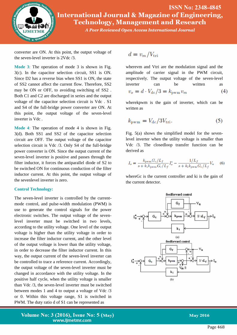
Fig. 5(a) shows the simplified model for the seven-
level inverter when the utility voltage is smaller than
Vdc /3. The closedloop transfer function can be
derived as
whereGc is the current controller and ki is the gain of
the current detector.

Page 469
Fig. 5.Model of the seven-level inverter under
different range of utility voltage, (a) in the range of
smaller than Vdc /3, (b) in the range of (Vdc /3,
2Vdc /3), (c) in the range of higher than 2Vdc /3.
CONTROL BLOCK:
The proposed solar power generation system consists
of a dc– dc power converter and a seven-level inverter.
The seven-level inverter converts the dc power into
high quality ac power and feeds it into the utility and
regulates the voltages of capacitors C1 and C2 . The
dc–dc power converter supplies two independent
voltage sources with multiple relationships and
performs maximum power point tracking (MPPT) in
order to extract the maximum output power from the
solar cell array.
Fig. 8. Control block: (a) seven-level inverter and
(b) dc–dc power converter.
A. Seven-Level Inverter:
Fig. 8(a) shows the control block diagram for the
seven-level inverter. The control object of the seven-
level inverter is its output current, which should be
sinusoidal and in phase with the utility voltage. The
utility voltage is detected by a voltage detector, and
then sent to a phase-lock loop (PLL) circuit in order to
generate a sinusoidal signal with unity amplitude. The
voltage of capacitor C2 is detected and then compared
with a setting voltage. The compared result is sent to a
PI controller. Then, the outputs of the PLL circuit and
the PI controller are sent to a multiplier to produce the
reference signal, while the output current of the seven-
level inverter is detected by a current detector.
B. DC–DC Power Converter:
Below figure shows the control block diagram for the
dc–dc power converter. The input for the DC-DC
power converter is the output of the solar cell array. A
ripple voltage with a frequency that is double that of
the utility appears in the voltages of C1 and C2 , when
the seven-level inverter feeds real power into the
utility. The MPPT function is degraded if the output
voltage of solar cell array contains a ripple voltage.
Therefore, the ripple voltages in C1 and C2 must be
blocked by the dc–dc power converter to provide
improved MPPT. Accordingly, dual control loops, an
outer voltage control loop and an inner current control
loop, are used to control the dc–dc power converter.
Since the output voltages of the DC-DC power
converter comprises the voltages of C1 and C2 , which
are controlled by the seven-level inverter, the outer
voltage control loop is used to regulate the output
voltage of the solar cell array. The inner current
control loop controls the inductor current so that it
approaches a constant current and blocks the ripple
voltages in C1 and C2 . The perturbation and
observation method is used to provide MPPT [24]. The
output voltage of the solar cell array and the inductor
current are detected and sent to a MPPT controller to
determine the desired output voltage for the solar cell
array.
EXPERIMENTAL RESULTS:

Page 470
To verify the performance of the proposed solar power
generation system, a prototype was developed with a
controller based on the DSP chip TMS320F28035. The
power rating of the prototype is 500 W, and the
prototype was used for a single-phase utility with 110
V and 60 Hz
MATLAB MODEL:
P&O MODEL:
OUTPUT WAVEFORMS:
CONCLUSION:
The solar power generation system to convert the dc
energy generated by a solar cell array into AC energy
that is fed into the utility. Solar power generation
system is composed of a dc–dc power converter and a
seven level inverter. The seven-level inverter contains
only six power electronic switches, which simplifies
the circuit configuration. Furthermore, only one power
electronic switch is switched at high frequency at any
time to generate the seven-level output voltage. This
reduces the switching power loss and improves the
power efficiency.

Page 471
The voltages of the two dc capacitors in the proposed
seven-level inverter are balanced automatically, so the
control circuit is simplified. In addition, the proposed
solar power generation system can effectively trace the
maximum power of solar cell array.
REFERENCES:
[1] R. A. Mastromauro, M. Liserre, and A.
Dell’Aquila, “Control issues in single-stage
photovoltaic systems: MPPT, current and voltage
control,” IEEE Trans. Ind. Informat., vol. 8, no. 2, pp.
241–254, May. 2012.
[2] Z. Zhao, M. Xu,Q. Chen, J. S. Jason Lai, andY. H.
Cho, “Derivation, analysis, and implementation of a
boost–buck converter-based high-efficiency pv
inverter,” IEEE Trans. Power Electron., vol. 27, no. 3,
pp. 1304–1313,
Mar. 2012.
[3] M. Hanif, M. Basu, and K. Gaughan,
“Understanding the operation of a Z-source inverter
for photovoltaic application with a design example,”
IET Power Electron., vol. 4, no. 3, pp. 278–287, 2011.
[4] J.-M. Shen, H. L. Jou, and J. C. Wu, “Novel
transformer-less grid connected power converter with
negative grounding for photovoltaic generation
system,” IEEE Trans. Power Electron., vol. 27, no. 4,
pp. 1818–1829, Apr. 2012.
[5] N. Mohan, T. M. Undeland, and W. P. Robbins,
Power Electronics Converters, Applications and
Design, Media Enhanced 3rd ed. New York, NY,
USA: Wiley, 2003.
[6] K. Hasegawa and H. Akagi, “Low-modulation-
index operation of a five level diode-clamped
Pwminverter with a dc-voltage-balancing circuit for a
motor drive,” IEEE Trans. Power Electron., vol. 27,
no. 8, pp. 3495–3505,
Aug. 2012.
[7] E. Pouresmaeil, D. Montesinos-Miracle, and O.
Gomis-Bellmunt, “Control scheme of three-level NPC
inverter for integration of renewable energy resources
into AC grid,” IEEE Syst. J., vol. 6, no. 2, pp. 242–
253, Jun. 2012.
[8] S. Srikanthan and M. K. Mishra, “DC capacitor
voltage equalization in neutral clamped inverters for
DSTATCOM application,” IEEE Trans. Ind. Electron.,
vol. 57, no. 8, pp. 2768–2775, Aug. 2010.
[9] M. Chaves, E. Margato, J. F. Silva, and S. F. Pinto,
“New approach in back-to-back m-level diode
clamped multilevel converter modeling and direct
current bus voltages balancing,” IET power Electron.
vol. 3, no.4, pp.578–589,2010.