approaches for reducing the cost of high pin · approaches for reducing the cost of high pin ......
TRANSCRIPT

Approaches for reducing the cost of high pin
count probe card testRudolph Technologies tells us how
Features, News Review, Industry Analysis, Research News and much more.
Free Weekly E News round up , go to www.siliconsemiconductor.net
Volume 35 Issue 3 2013 @siliconsemi www.siliconsemiconductor.net
Diamond coating expand options
Raising battery life with silicon
Optimising integrated system
Nikon get order for 450mm scanner
New products at SEMICON West
Front Cover SiS v1.indd 1 02/08/2013 09:38

Contact Watlow® today for the latest thermal solutions for semiconductor applications.Contact Watlow® today for the latest thermal Contact Watlow® today for the latest thermal Contact Watlow® today for the latest thermal Contact Watlow® today for the latest thermal Contact Watlow® today for the latest thermal Contact Watlow® today for the latest thermal Contact Watlow® today for the latest thermal Contact Watlow® today for the latest thermal Contact Watlow® today for the latest thermal Contact Watlow® today for the latest thermal Contact Watlow® today for the latest thermal Contact Watlow® today for the latest thermal Contact Watlow® today for the latest thermal Contact Watlow® today for the latest thermal Contact Watlow® today for the latest thermal Contact Watlow® today for the latest thermal Contact Watlow® today for the latest thermal Contact Watlow® today for the latest thermal Contact Watlow® today for the latest thermal Contact Watlow® today for the latest thermal Contact Watlow® today for the latest thermal Contact Watlow® today for the latest thermal Contact Watlow® today for the latest thermal Contact Watlow® today for the latest thermal Contact Watlow® today for the latest thermal Contact Watlow® today for the latest thermal Contact Watlow® today for the latest thermal Contact Watlow® today for the latest thermal Contact Watlow® today for the latest thermal Contact Watlow® today for the latest thermal Contact Watlow® today for the latest thermal Contact Watlow® today for the latest thermal Contact Watlow® today for the latest thermal Contact Watlow® today for the latest thermal solutions for semiconductor applications.solutions for semiconductor applications.solutions for semiconductor applications.solutions for semiconductor applications.solutions for semiconductor applications.solutions for semiconductor applications.solutions for semiconductor applications.solutions for semiconductor applications.solutions for semiconductor applications.solutions for semiconductor applications.solutions for semiconductor applications.solutions for semiconductor applications.solutions for semiconductor applications.solutions for semiconductor applications.solutions for semiconductor applications.solutions for semiconductor applications.solutions for semiconductor applications.solutions for semiconductor applications.solutions for semiconductor applications.solutions for semiconductor applications.solutions for semiconductor applications.solutions for semiconductor applications.solutions for semiconductor applications.solutions for semiconductor applications.solutions for semiconductor applications.solutions for semiconductor applications.solutions for semiconductor applications.solutions for semiconductor applications.solutions for semiconductor applications.solutions for semiconductor applications.solutions for semiconductor applications.solutions for semiconductor applications.solutions for semiconductor applications.solutions for semiconductor applications.Contact Watlow® today for the latest thermal Contact Watlow® today for the latest thermal Contact Watlow® today for the latest thermal Contact Watlow® today for the latest thermal Contact Watlow® today for the latest thermal Contact Watlow® today for the latest thermal Contact Watlow® today for the latest thermal Contact Watlow® today for the latest thermal Contact Watlow® today for the latest thermal Contact Watlow® today for the latest thermal Contact Watlow® today for the latest thermal Contact Watlow® today for the latest thermal Contact Watlow® today for the latest thermal Contact Watlow® today for the latest thermal Contact Watlow® today for the latest thermal Contact Watlow® today for the latest thermal solutions for semiconductor applications.solutions for semiconductor applications.solutions for semiconductor applications.solutions for semiconductor applications.solutions for semiconductor applications.solutions for semiconductor applications.solutions for semiconductor applications.solutions for semiconductor applications.solutions for semiconductor applications.solutions for semiconductor applications.solutions for semiconductor applications.solutions for semiconductor applications.solutions for semiconductor applications.
Optimize the Thermal Performance of your
Process Equipment.
Watlow provides innovative
solutions to help process tool
manufacturers meet the needs of the
semiconductor technology roadmap.
Our approach is to work collaboratively
to help solve complex thermal
challenges associated with state-of-the-
art manufacturing processes; helping
to improve yield, throughput and cost
of ownership. This includes innovative
heaters, controllers and sensors for use
in front-end and back-end applications
such as CVD, PECVD, Etch, Diffusion,
Bonding, IC test and more.
Extensive computational tools enable product designs to be highly refined for ultimate performance.
Multi-zone circuit layouts in a polyimide construction are highly customized to deliver exacting performance up to 250°C.
EZ-ZONE® RM Multi-loop controllers are fully scalable with up to 152 PID Loops and 256 monitor points per system.
ASSURANT™ gas and pump line heaters feature high temperature capabilities with low outgassing.
Optimize the Thermal Optimize the Thermal Optimize the Thermal Optimize the Thermal Optimize the Thermal Optimize the Thermal Optimize the Thermal Optimize the Thermal Optimize the Thermal Optimize the Thermal Optimize the Thermal Optimize the Thermal Optimize the Thermal Optimize the Thermal Optimize the Thermal Optimize the Thermal Optimize the Thermal Optimize the Thermal Optimize the Thermal Optimize the Thermal Optimize the Thermal Optimize the Thermal Optimize the Thermal Optimize the Thermal Optimize the Thermal Optimize the Thermal Optimize the Thermal Optimize the Thermal Optimize the Thermal Optimize the Thermal Optimize the Thermal Optimize the Thermal Performance of your Performance of your Performance of your Performance of your Performance of your Performance of your Performance of your Performance of your Performance of your Performance of your Performance of your Performance of your Performance of your Performance of your Performance of your Performance of your Performance of your Performance of your Performance of your Performance of your Performance of your Performance of your Performance of your Performance of your Performance of your Performance of your Performance of your Performance of your Performance of your Performance of your Performance of your Performance of your Performance of your Performance of your Performance of your Performance of your Performance of your Performance of your Performance of your
Process Equipment.Process Equipment.Process Equipment.Process Equipment.Process Equipment.Process Equipment.Process Equipment.Process Equipment.Process Equipment.Process Equipment.Process Equipment.Process Equipment.Process Equipment.Process Equipment.Process Equipment.Process Equipment.Process Equipment.Process Equipment.Process Equipment.Process Equipment.Process Equipment.Process Equipment.Process Equipment.Process Equipment.Process Equipment.Process Equipment.Process Equipment.Process Equipment.Process Equipment.Process Equipment.Process Equipment.Process Equipment.Process Equipment.Process Equipment.Process Equipment.Process Equipment.Process Equipment.Process Equipment.Process Equipment.Process Equipment.Process Equipment.Process Equipment.Process Equipment.Process Equipment.Process Equipment.
Extensive computational tools enable product designs to be highly refined for ultimate performance.
European Technical Sales Offices
Germany +49 (0) 7253-9400-0 [email protected]
France +33 1 41 32 79 70 [email protected]
Italy +39 02 4588841 [email protected]
Spain +34 91 675 1292 [email protected]
UK +44 (0) 115-964-0777 [email protected]

executiveviewby Su Westwater, News Editor Silicon Semiconductor and Compound Semiconductor
Silicon Semiconductor is published four times a year on a controlled circulation basis. Non-qualifying individuals can subscribe at: £105.00/e158 pa (UK & Europe), £138.00 pa (air mail), $198 pa (USA). Cover price £4.50. All information herein is believed to be correct at time of going to press. The publisher does not accept responsibility for any errors and omissions. The views expressed in this publication are not necessarily those of the publisher. Every effort has been made to obtain copyright permission for the material contained in this publication. Angel Business Communications Ltd will be happy to acknowledge any copyright oversights in a subsequent issue of the publication. Angel Business Communications Ltd © Copyright 2013. All rights reserved. Contents may not be reproduced in whole or part without the written consent of the publishers. The paper used within this magazine is produced by chain of custody certified manufacturers, guaranteeing sustainable sourcing. US mailing information: Silicon Semiconductor (ISSN 1096-598X) is published four times a year for a subscription of $198 by Angel Business Communications Ltd, Hannay House, 39 Clarendon Road, Watford, Herts WD17 1JA, UK. Periodicals postage paid at Rahway, NJ. POSTMASTER: send address changes to: Silicon Semiconductor, c/o Mercury International Ltd, 365 Blair Road, Avenel, NJ 07001. Printed by: Pensord Press. © Copyright 2013. ISSN 2050-7798 (Print) ISSN 2050-7801 (Online).
News Editor Dr. Su Westwater [email protected] of SEMI Publishing Jackie Cannon [email protected] +44 (0)1923 690205Senior Sales Executive Robin Halder [email protected]
+44 (0)2476 718109Sales Manager Shehzad Munshi [email protected] +44 (0)1923 690215USA Representatives Tom Brun Brun Media E: [email protected] Tel: 724 539-2404 Janice Jenkins E: [email protected] Tel: 724-929-3550Director of Logistics Sharon Cowley [email protected] +44 (0)1923 690200Design & Production Manager Mitchell Gaynor [email protected] +44 (0)1923 690214Circulation Director Jan Smoothy [email protected] +44 (0)1923 690200
Circulation & Subscriptions Assistant Annette Weatherilt [email protected] +44 (0)1923 690220Chief Operating Officer Stephen Whitehurst [email protected] +44 (0)2476 718970Directors Bill Dunlop Uprichard – CEO, Stephen Whitehurst – COO, Jan Smoothy – CFO, Jackie Cannon, Scott Adams, Sharon Cowley, Sukhi Bhadal
Published by Angel Business Communications Ltd, Hannay House, 39 Clarendon Road, Watford, Herts WD17 1JA, UK. T: +44 (0)1923 690200 F: +44 (0)1923 690201 E: [email protected]
Angel Business Communications Ltd, Unit 6, Bow Court, Fletchworth Gate, Burnsall Road, Coventry CV5 6SP, UK. T: +44 (0)2476 718 970 F: +44 (0)2476 718 971 E: [email protected]
Issue III 2013 www.siliconsemiconductor.net 3
How many people do you need to change a light bulb? None - it’s an LED bulb
GALLIUM NITRIDE-ON-SILICON is a hot topic for LEDs and power devices. But LEDs could be the game changer - in the immediate future at least - as LED bulbs can last a lifetime. With new government regulations to make our world more environmentally friendly, and the demise of incandescent bulbs, LEDs are on the rise. It was in the late 1800s when Thomas Edison invented the first commercially practical incandescent light that some of us are still using. But it’s time for us to move on. In the last ten years, there have been a cluster of companies targeting the massive lighting market. The question is who will be the quickest to come up with the goods? We want the brightest, eco-friendliest most versatile LED bulb at the lowest cost which is also easy on the eye. It’s a tall order. Most white to blue semiconductor LEDs incorporate the wide bandgap compound semiconductor gallium nitride (GaN). And you may be spoilt for choice with the different substrates that can be used in making the device - these include sapphire, silicon carbide, silicon and GaN itself. Many of these substrates are costly though. The exception is silicon, which comes in large substrate sizes such as 6” and 8”. So what are the challenges of growing GaN on silicon?Firstly the difference in lattice parameter between the most prevalent silicon <111> and GaN is large (around 17%). One
of the key aspects to counter this is growing a layer (often AlN) - this layer prevents chemical reactions between Ga and silicon and makes the wafer behave like a substrate having lattice parameters closer to that of GaN. Then the buffer layer (mainly AlGaN) is grown to further reduce the mismatch. There is also a 52% thermal mismatch between GaN and silicon. This means that once the wafer is cooled down after growth, the GaN will contract at a different rate to the silicon substrate. And knowledge of III-Vs on silicon is not as established as other technologies such as GaN-on-sapphire. Having said that, the plus side would work two-fold. Silicon
substrates are cheap and also, growing on silicon would enable fabs to use their existing tools without having to invest in costly alternative
equipment. Current players in the GaN-on-Si market include Toshiba and Plessey. Both companies have recently launched LEDs for the lighting market. But efficiencies are still relatively low. Using technology initiated
by Colin Humphrey’s group at Cambridge, Plessey and Aixtron are working together to optimise
a process using a close coupled showerhead (CCS) reactor capable of growing 6 inch GaN-on-Si. Apart from Toshiba, competitors include Lattice Power, Transphorm, Azzurro, Infineon, Philips Lumileds, Samsung and imec (and partners). Soitec, Azzurro, Kyma, Translucent and EpiGaN provide GaN-on-Si templates. So only time and investment will tell who comes out on top.
Executive View v1.indd 3 02/08/2013 09:52

MEETING LITHOGRAPHY CHALLENGES HEAD-ON
Large fi eld of view (52mm x 66mm)
30 reticle library with four-reticle wheel
On-the-fl y auto focus for each exposure
Warped wafer handling
Superior depth of focus for thick resists
Substrate and size fl exibility (450mm, reconstituted wafers, square interposers, etc.)
Stepper redefi ned
JetStep™ Advanced PackagingLithography SystemAdvancing Tomorrow’s Technology
-ON
rs, etc.)
JetStep™ Advanced Packaging
Untitled-1 1 02/08/2013 09:33
Issue III 2013 www.siliconsemiconductor.net 5
contentsVolume 35 Issue 3 2013 ConneCtIng the SILICon SemIConduCtor CommunIty
22 Raising battery life with silicon all the rage A novel tetrahedral structure consisting of boron and silicon, serving as an electrode material in lithium borosilicide (LiBSi2), forms open channels. This offers, in principle, the possibility to store and release lithium atoms.
24 Flat lens makes it better to see you with A novel new lens could lead to improved photolithography, nanoscale manipulation and manufacturing and high-resolution 3D imaging.
26 3D defect detection fills the 450mm gap Scientists develop technique to create a 3D image quickly and non-destructively that enable fast and non-destructive detection of d efects at the nanometre level.
28 The crystalline silicon solar-to-fuel roadmap New analysis by MIT researchers points the way forward to optimising efficiency of an integrated system for harvesting sunlight to make storable fuel.
30 Approaches for reducing the cost of high pin count probe card test The cost of high pin count probe card testing can be reduced significantly. In most cases, no-load measurements can provide all the information needed.
News
06 Crocus gets €34m funding
07 AMAT to capitalise on mobile era
08 CEA-Leti and Alchimer bring high aspect ratio TSVs
10 Dow Corning & imec to advance 3D IC packaging
11 Nujira gears up for mass production
12 Nikon to receive order for 450mm scanner for G450
13 MEMS expertise to aid IR detector market
14 Comms IC market to exceed computer IC market
15 Processing capacity: 450mm not as promising as 300mm
Products
34 Robot automated transport for cleanrooms revealed
35 Solder mask issues solved
36 SSEC unveils single wafer wet processing tools
37 EV Group tool pushes the limits on 3D ICs
38 KLA-Tencor defect analysis on another level
39 AMAT tool analyses defects in 3D Transistors and nodes
Magazine and Front Cover designed by Mitch Gaynor
Approaches for reducing the cost of high pin
count probe card testRudolph Technologies tells us how
Features, News Review, Industry Analysis, Research News and much more.
Free Weekly E News round up , go to www.siliconsemiconductor.net
Volume 35 Issue 3 2013 @siliconsemi www.siliconsemiconductor.net
Diamond coating expand options
Raising battery life with silicon
Optimising integrated system
Nikon get order for 450mm scanner
New products at SEMICON West
Front Cover SiS v1.indd 1 02/08/2013 09:38
22
24
28
36
features
Contents v1.indd 5 02/08/2013 10:33

6 www.siliconsemiconductor.net Issue III 2013
NEWS REVIEW
Crocus gets €34m fundingCROCUS TECHNOLOGY, a developer of magnetically enhanced semiconductor technologies for mobile security, embedded microcontrollers, harsh environment electronics and magnetic sensors, has raised EUR €34 million (US$ 45 million) in additional capital.
A new private investor, Industrial Investors, joined the round led by Idinvest Partners. Major investors Sofi nnova Ventures, Innovation Capital, Nanodimension and Ventech also participated, underscoring seven years’ support.
Shareholder Rusnano has also contributed to the funding.The new funding will enable Crocus to signifi cantly ramp up manufacturing at TowerJazz Semiconductors. It will also enable Crocus to qualify its jointly owned fab, Crocus Nano Electronics, and release the fi rst engineering wafers during the summer
Together with its partner IBM, Crocus hopes to accelerate the development of Generation 3 technology for Crocus’ secure microcontrollers. These secure microcontrollers will target primarily high-end smart cards, a market that reached 7.9 billion units in 2012. This is according to ABI Research, in a report from May 2013. Crocus aims to capture 30 percent of this market by bringing smart card makers new enhanced-performance features at lower cost. Crocus also aims to launch a magnetic sensor product line, which leverages the same proprietary Magnetic Logic Unit (MLU)
manufacturing platform technology, in a market expected to reach the $2 billion per year mark in the near term.
“Crocus is now fully funded to deliver on the last key milestone in the industrial processing of its now mature Magnetic Logic Unit technology,” says Bertrand Cambou, CEO and executive chairman of Crocus Technology.
“The commitment from our impressive group of investors along with the validation of our technology by strategic customers put us in a good position to prepare for product revenue around the end of this year. Combined with our steadily growing licensing and services business, we anticipate reaching cash fl ow break-even point by the end of next year,” concludes Cambou.
Crocus has pioneered the development of Magnetic Logic Unit (MLU), a CMOS-based rugged technology. MLUs bring important new advantages in speed, performance and security at lower cost to a range of next-generation electronics. It brings high sensitivity, low-noise, high temperature performance to magnetic sensors.
New subsidiary expands wet processing division at ClassOne CLASSONE EQUIPMENT has made signifi cant investments in the growth and expansion of its Wet Processing Division in response to increased market demand.
A Design and Development Centre has been opened in Kalispell, Montana, staffed with several industry veterans who represent over 200 years of cumulative industry experience, who will focus on new product design and development. Corporate and refurbishment activities will remain at ClassOne’s headquarters in Atlanta, Georgia.
“We are thrilled with the strong customer response to ClassOne’s industry-leading products and support. We have expanded the division to enhance our sales and support of legacy Semitool equipment worldwide as well as to design and manufacture new state-of-the-art upgrades and platforms that address emerging markets such as MEMS, Nanotech, LED and RF Power Devices,” says Byron Exarcos, ClassOne’s President.
Hi adds, “Semitool’s acquisition left a void in the market for mature fabs and emerging technologies that use 75 to 200mm substrates. ClassOne is meeting the growing demand for cost effective, reliable, and long-term support for popular tools such as the Spray Solvent, Spray Acid and Equinox tools. The wide-spread adoption of our lift-and-rotate and robot refurbishment programs gives testimony to that fact.”
The new facility in Kalispell will be operated under the name of ClassOne. The executive team includes: Win Carpenter VP Wet Process Division; Tim McGlenn VP of Operations; and Kevin Witt VP Technology; all of whom previously held senior positions at Semitool.
Cohu to supply multiple toolsCOHU has a multi-unit order for T-Core thermal subsystems that optimise testing of application processors used in mobile computing. The company has not specifi ed how many were ordered.
Cohu’s T-Core thermal technology enables higher test yield for ICs that power a wide range of smartphones, tablets, and other consumer devices. T-Core can be integrated in Cohu’s production test handlers or in batch test systems for cost-effective, parallel testing of hundreds of ICs.
“We are pleased to see our thermal
technology that is today the benchmark for testing mid and high power processors, being used in new applications for the mobile market,” says Luis Müller, President of Cohu’s Semiconductor Equipment Group.Cohu’s thermal technology optimises test yield of high-end devices, including microprocessors used in laptops, PCs and cloud-servers, as well as graphic processors, mobile application processors and a variety of other complex ICs. Current T-Core confi gurations range from single to over 500 devices tested in parallel at 8W to 350W power dissipation.
News SiS v1.indd 6 18/07/2013 12:37

Issue III 2013 www.siliconsemiconductor.net 7
NEWS REVIEW
SPECIALTY FOUNDRY TowerJaz has extended its business relationship with International Rectifi er (IR) which specialises in power management technology. The fi rms have entered into a seven-year agreement where TowerJazz will manufacture multiple product families for IR.
IR chose to extend its relationship with TowerJazz due to a history of success in working with TowerJazz’s TOPS (Transfer Optimisation and Process Services) business unit.
This is a group with engineering profi ciency and models that enable Integrated Device Manufacturers (IDMs) the shortest qualifi cation time and fastest time-to-market for
moving their manufacturing into high volume foundries. As part of this latest collaboration, IR will use multiple fabs from TowerJazz.
“IR has enjoyed a strong relationship with TowerJazz, recognising the company as an International Rectifi er Supplier of the Year 2012 based upon criteria including alignment of business goals, manufacturing fl exibility and responsiveness.
With its goal to be the specialty foundry leader, TowerJazz continues to meet our business needs and we are pleased to enter into this agreement,” says Oleg Khaykin, President and Chief Executive Offi cer, International Rectifi er.
AMAT to capitalise on mobile eraAT A MEETING of the company’s top investors and equity analysts, Applied Materials (AMAT) demonstrated plans to drive profi table growth by using its expertise in Precision Materials Engineering.
The fi rm wants to help customers overcome the engineering challenges of delivering more powerful, battery-effi cient and visually compelling digital devices to a growing global market.
The evolution of transistor and display technologies propelled by consumer demand for increased mobility presents Applied Materials with new opportunities for profi table growth.
Ever-growing consumer demand for faster processors, longer battery life, and bigger and better displays is creating major device performance and yield challenges for semiconductor and display manufacturers - challenges that Applied Materials is positioned to solve.“Semiconductor and display makers are racing to deliver the new mobile products consumers demand,” said Mike Splinter, chairman and chief executive offi cer. “The war for mobility leadership will be won by materials innovation that is enabled by Applied Materials.”
The industry is re-engineering transistor designs, driving the need for new materials and new ways of handling those materials, as manufacturers look beyond shrinking lithography geometries to achieve performance gains. Applied Materials’ know-how in Precision Materials Engineering is critical to solving customers’ toughest device challenges, and enabling further innovations in 3D transistors and display manufacturing.“Our leadership in Precision Materials Engineering is what makes Applied unique and provides us with great opportunities for profi table growth,” said Gary Dickerson, president of Applied Materials. “We are enabling major mobility infl ections that bring more advanced features and improved battery life in next-generation mobile devices.”
Robert Halliday, senior vice president and chief fi nancial offi cer, presented the company’s new fi nancial model, which outlines increased profi tability goals for non-GAAP adjusted earnings per share of $1.50 - $2.15 by fi scal 2016.
This model accounts for a number of factors including varying levels of industry investment and market share assumptions.“Industry infl ections and the need for new materials to address technology challenges play in our favour and position us as an increasingly strategic and valuable partner to our customers, which we believe will lead to further opportunities to expand our total available market,” said Halliday. “Our new fi nancial targets are supported by our investment in cutting-edge innovation, focus on execution and discipline to lower costs as we pursue future profi table growth.”
Randhir Thakur, executive vice president and general manager of the Silicon Systems Group, highlighted several new products and discussed specifi c growth opportunities in transistor, interconnect, patterning and yield. “As we enter the second half of 2013, our product pipeline has us strongly positioned with a range of innovations that benefi t our customers as they navigate coming technology infl ections,” he said.“Our new transistor technologies will help customers meet the insatiable demand for more effi cient
computing power, while our interconnect developments ensure device reliability at the backend.
The momentum we are building with these innovations will help customers accelerate their transitions to 1Xnm technology nodes and usher in a new era of mobile products,” added Thakur.Delivering updates on Applied Materials’ display equipment business was Ali Salehpour, group vice president, general manager, Energy and Environmental Solutions and Display business groups.
“The display industry is experiencing the most signifi cant technology transition in two decades, implementing new metal oxide and low temperature polysilicon (LTPS) materials to manufacture higher resolution LCD and organic light-emitting diode (OLED) displays,” said Salehpour.
IR and TowerJazz extend relationship
News SiS v1.indd 7 18/07/2013 12:38

8 www.siliconsemiconductor.net Issue III 2013
NEWS REVIEW
CEA-LETI AND EV GROUP (EVG) have launched a three-year common lab to optimise temporary and permanent-bonding technologies related to 3D TSV integration and all direct bonding heterostructures. The lab, continues more than 10 years of collaboration between the two organisations, is focusing on hardware, software and process development.
“Temporary and permanent bonding equipment and process solutions
are key product offerings for EVG,” says Markus Wimplinger, EVG’s corporate technology development and IP director. “This project leverages CEA-Leti’s global leadership in wafer-bonding research and EVG’s unparalleled expertise in developing wafer bonding equipment and process technology. Like all common labs that Leti creates with its partners, this project is designed to produce specifi c, practical solutions that address current and future market requirements,”
comments Laurent Malier, CEA-Leti CEO. “This collaboration is targeting results that will make 3D TSV integration more effi cient and cost effective and open new areas of wafer bonding using covalent bonding at room temperature.
Bringing these approaches to high-volume manufacturing with reliable wafer bonding requires innovative fabrication processes,” adds Fabrice Geiger, head of Leti’s Silicon Technology division.
CEA-Leti and Alchimer bring high aspect ratio TSVsTHE SEMICONDUCTOR INDUSTRY continues to actively explore 3D integration ;achieving high aspect ratio TSVs remains a major challenge; current techniques are limited to about 10:1. Now CEA-Leti has validated Alchimer’s wet nanometric fi lm deposition processes for 300mm high volume manufacturing.
Together, the fi rms will evaluate Alchimer’s Electrografting (eG) and Chemicalgrafting (cG) processes for isolation, barrier and seed layers. When combined, Alchimer’s wet deposition processes have been demonstrated to achieve 20:1 aspect ratio through silicon vias (TSVs) due to their ability to coat conformally regardless of via topography, diameter or depth.
3D integration is moving towards a “via middle” approach where TSVs are formed after front-end processes, but prior to stacking. Several applications are in the development phase, leading to constraints and different specifi cations for TSVs. Alchimer believes its technology shows the potential to break through existing barriers to achieve high aspect ratio TSVs. The collaboration with Leti will evaluate the potential of its technology and its suitability for high-volume manufacturing.
“Current techniques, such as PECVD isolation and iPVD metallisation, have performance limitations that are limiting achievable TSVs to 10:1 aspect ratios,” says Bruno Morel, CEO of Alchimer. “Our 3D TSV products have unequivocally demonstrated their ability to deliver 20:1 aspect ratios at a signifi cantly reduced cost as compared to current approaches. Now it is critical to validate the products’ full potential for 300mm high-volume manufacturing as well as to study their compatibility with the overall 3D integration process. Leti’s leading 3D expertise and world-class infrastructure will allow us to do that.”
“Collaborating with Alchimer fi ts perfectly our strategy of delivering innovative solutions to industry,” adds Fabrice Geiger, head of Leti’s Silicon Technology Division. “Alchimer’s eG technology is a promising, cost-effective and breakthrough solution to address the challenges of future 3D TSV integration. Through this collaboration, Alchimer will have access to Leti’s expertise in the domain of 3D TSV integration and its world-class 300mm 3D platform capabilities.”
Ultratech wins repeat order for lithography tool from major OSATULTRATECH, INC. has received a repeat order from a leading outsourced semiconductor assembly and test (OSAT) company in Asia. The AP300W lithography system built on Ultratech’s customisable Unity Platform will be utilised for wafer-level packaging (WLP) applications to support growth driven by communication devices. As the advanced packaging technology requirements evolve, OSATs will play an important role in establishing the supply chain.
“Demand for thinner mobile communication devices such as smartphones and tablets are driving much of the growth in WLP,” according to Jan Vardaman , president and founder of TechSearch International. “Many of the suppliers of the integrated circuits used in these products depend on OSATs to meet their production needs. It is expected that the OSAT expansion will continue over the next several years to address this growth opportunity.”
Ultratech Vice President, Advanced Packaging Technology/Nanotechnology Market Manish Ranjan adds, “Ultratech has maintained a leading market position over the last decade by delivering outstanding production performance with superior cost-of-ownership solutions. We look forward to working closely with our customers in the OSAT segment to support their high-volume production ramps.”
Leti and EV Group unite on wafer bonding
News SiS v1.indd 8 18/07/2013 12:38

Transfer valve for 450 mm wafer technology L-MOTION valve for corrosive high-end semiconductor applications
Real L-MOTION valve technology assures uniform seal compression
Excellent gate seal lifetime
Highest yield through low particle count and high speed
Lowest vibration
Fast and easy gate exchange via top service cover
www.vatvalve.com
PLASMAPLASMAPLASMAInstrumental in changeLeading plasma process innovation
Plasma Etch & Deposition
Atomic Layer Deposition
Ion Beam Etch & Deposition
Deep Silicon Etch
Oxford Instruments Plasma Technology is turning smart science into world class products with its flexible systems for precise and repeatable etching, deposition and growth of micro and nano structures
For more information, please contact Oxford Instruments Plasma Technology: Tel: +44 (0)1934 837 000 Email: [email protected]
www.oxford-instruments.com/plasma
Untitled-3 1 31/05/2013 14:15

10 www.siliconsemiconductor.net Issue III 2013
NEWS REVIEW
Dow Corning & imec to advance 3D IC packagingDow Corning is one of the newest member organisations to join imec, a leading research centre for the advancement of nano-electronics.
The announcement signals expanded opportunities for both organisations to combine their expertise toward the development and broader adoption of 3D integrated circuit (iC) packaging technologies, wherein iC chips are stacked in vertical 3D architectures.
“This move is a natural and strategic step for Dow Corning and imec, as we both believe collaborative innovation is as critical to industry leadership as native expertise,” says Andrew Ho, global industry director, Advanced Semiconductor Materials at Dow Corning.
“our access to imec’s world-class resources and expertise will not only help us further refine our unique temporary bonding solution, it will allow imec to leverage that solution to advance integration of the 3D iC packaging process that they’ve been developing for years,” adds Ho.
By integrating multiple chips into a single package, 3D iC technology promises to reduce form factor and power consumption, and increase bandwidth to enable more efficient inter-chip communication for next-generation microelectronics devices. Yet, before 3D iC fabrication can see broader adoption, it will require innovative advances in materials and processing technologies.
The photo above shows a thin silicon wafer on dicing frame after successful debonding from a silicon carrier wafer at imec, using Dow Corning’s silicone-based temporary bonding solution.one of the key challenges imec is tackling is the bonding of the device wafer to a carrier wafer, prior to wafer thinning, and the safe debonding of the thin wafer after completion of backside processing.
This was Dow Corning’s goal when designing its Temporary Bonding Solution, aims at simple processing using a bi-layer concept comprising an adhesive and release layer. The technology also enables room-temperature bonding and debonding
processes based on standard manufacturing methods. Together with imec, Dow Corning will explore its temporary bonding CMoS-compatible solution for 3D Through-Silicon-Via (TSV) semiconductor packaging. The collaboration will aim to further expand the technology’s ability to achieve simple, cost-effective bonding-debonding techniques compatible with standard manufacturing processes.
“imec’s precompetitive programs are an essential platform for industry leaders to share the risk and cost of advanced research. As one of the semiconductor industry’s most proven pioneers in advanced silicone-based solutions, Dow Corning brings valuable materials and processing expertise to imec’s global network of innovators – as well as a key enabling technology for TSV fabrication,” says Eric Beyne, program director 3D System integration at imec.
“we look forward to collaborating closely with our newest member ” adds Beyne.
Picosun reveals 450mm ALD systemPiCoSun oY, has introduced the PiCoSun P-1000 ultra-large scale batch ALD tool. This is the latest addition to the fully automated, high throughput PiCoSun P-series of Atomic Layer Deposition (ALD) tools. The P-1000 system shares the same core construction as the smaller PiCoSun systems. Picosun says that already the first process results with the P-1000 ALD system have been excellent.
when using an aluminium oxide process on 400mm x 600mm glass sheets in a batch of 30 pieces, a film thickness non-uniformity of only 1.55 percent (1σ) was achieved, while maintaining a temperature distribution non-uniformity of only ± 2oC inside the reaction chamber.The PiCoSun P-1000 batch ALD reactor’s deposition chamber can be made according to the customer’s specified substrate size. As square, the
maximum cross section of the chamber is 470mm x 470mm, and as circular, the maximum diameter is 600mm. The maximum height of the chamber is 700mm.
The square chamber is optimal for coating batches of 450mm diameter silicon wafers - the next step in the evolution of the modern semiconductor manufacturing technology - or batches of large glass or metal sheets. Also smaller silicon wafers or 156mm x 156mm square solar wafers can be processed with their own, specifically designed sample holders. Alternatively, when equipped with the cylindrical reaction chamber the configuration is ideal for processing large batches of 3D objects. The P-1000 system comes with a separate electronics and precursor source cabinet designed for fast and easy maintenance, while keeping the tool frame and footprint
plain and compact to save expensive facility space.
Eight separate precursor manifolds and software capable of controlling 12 individual precursor sources ensure the highest level of flexibility in process development and ALD material selection.Timo Malinen, Chief operating officer of Picosun, summarises by saying, “Launching the P-1000 ultra-large batch ALD tool marks an important milestone in establishing Picosun as the leading industrial supplier of large-scale ALD solutions.”
“while the ALD technology makes breakthroughs in more and more new industries, the demands for processing equipment capacity and flexibility regarding sample size, shape, and process throughput expand accordingly,” he adds.
News SiS v1.indd 10 18/07/2013 12:38

Issue III 2013 www.siliconsemiconductor.net 11
NEWS REVIEW
Nujira has extended its partnership agreement with Towerjazz, as its new NCT-L1300 ET chip is geared up for volume production.
With Envelope Tracking (ET) technology heading towards a 100 percent attach rate in 4G smartphones by 2014, Nujira is building a network of supply chain partners to ensure its chip enters the market seamlessly and is able to meet volume and quality demands.
ET is the leading technology being developed to reduce power consumption of 4G smartphones in order to extend battery life. ET dynamically adapts the Power amplifier (Pa) supply voltage to the signal amplitude, and thus dramatically reducing the power consumption of the Pa that transmits the signal to the antenna.
annual revenue for analogue application specific iCs for 4G mobile handsets forecast to grow to $2.9 billion by 2017, an estimated CaGr of 29 percent.anyone who uses 4G phones experiences an empty battery much earlier than with 3G, sometimes in the middle of the day.
There are several technologies being developed in order to reduce power consumption of such phones. But recently, ET interfaces have become standardised on LTE basebands, paving the way to a very high adoption rate of
Nujira gears up for mass productionthis technology.Nujira believes it is well positioned to take a large portion of the ET market. according to global information provider, iHS, the annual revenue for analogue application specific iCs for 4G mobile handsets is forecast to grow from $827 million in 2012 to $2.9 billion by 2017, a compound annual growth rate (CaGr) of 29 percent for the next five years.
Nujira selected Towerjazz, a specialty foundry and fifth largest foundry worldwide, as its manufacturing partner in early 2012.
The NCT-L1300 is fabricated in Towerjazz’s 0.18 µm rF CMOS technology, used in hundreds of millions of rF front end devices, with additional uniquely fitted HV modules. Nujira’s NCT-L1300 delivers power conversion efficiencies in excess of 80 percent, effectively doubling the efficiency of existing solutions. Tim Haynes, CEO, Nujira says, “Over the last year we’ve built an excellent relationship with Towerjazz; its processes offer us the ideal combination of high performance analogue and power management capabilities. Nujira’s ET iCs have the highest bandwidth, widest voltage range, fastest slew rates, and lowest output impedance in the market,
placing significant demands on the underlying process technology. Towerjazz meets all of these stringent requirements and works closely with us to ensure a high success rate and competitive time to market.”
“as the world’s largest specialty analogue foundry, Towerjazz offers us the experience and capacity to address the high volume smartphone market, and enables us to meet the price points demanded by the
world’s largest smartphone vendors.
Moving our new iC into volume production is a critical step for our business, and with its process expertise, wafer capacity and security of supply across multiple fabs, Towerjazz is the right foundry partner for Nujira,” adds Haynes.
“Nujira’s technology has huge potential, with ET technology heading towards a 100 percent attach rate in LTE smartphones in 2014. We are excited to be their partner and to be supporting them in volume production of their NCT-L1300. Nujira’s chips combine wireless communications and smart energy, which are two high growth focus areas for Towerjazz,” notes russell Ellwanger,Towerjazz CEO.
SV PrOBE PTE. LTd. (SV), a supplier of high-performance probe cards, has entered into a business transfer agreement to purchase certain probe card business, technologies, intellectual property rights and assets of Tokyo Cathode Laboratory (TCL).
Probe cards are essential tools in the electrical testing of semiconductor wafers before they are diced, packaged and assembled in electronic products such as tablets, smart phones, computers and digital media players. This acquisition will create a stronger product portfolio for SV, place the company in a more competitive position within the iC testing market and give SV Probe an advantage with access
SV Probe acquires Tokyo Cathode Laboratory assetsto the large japanese probe card market. SV Probe will acquire TCL’s shares in its subsidiaries in Singapore, Taiwan, Hong Kong and Guangzhou, China, along with the assets and business of TCL and its japan subsidiaries, held or used in the marketing, manufacturing and distribution of certain probe card products. TCL is a probe card manufacturer based in japan with a substantial production and distribution network across asia. The company possesses strong probe card capabilities, specifically CMOS image Sensor (CiS) and Liquid Crystal display (LCd), which are used mainly in smart phones, tablets, digital cameras and other imaging devices.
TCL has developed proprietary cantilever probe materials along with build and assembly processes that extend the capability of its products utilized in different device testing applications. as a result, TCL has gained a number of key CiS, LCd, and logic/SOC customers in japan and throughout asian market.“TCL’s extensive knowledge in probe card technologies and strong customer relationships will create new revenue opportunities for SV Probe,” says Kevin Kurtz, President & CEO of SV Probe. “This acquisition will enable SV Probe to increase its participation in the valuable and significant japanese probe card market.”
News SiS v1.indd 11 18/07/2013 16:22

12 www.siliconsemiconductor.net Issue III 2013
NEWS REVIEW
FujiTSu SEMiCONduCTOr LiMiTEd (Fujitsu) has released the MB51T008a, a silicon substrate-based GaN power device that has a breakdown voltage of 150 V. The new device, which enables normally-off operations, is capable of achieving roughly one half the fi gure of merit (FOM) of silicon-based power devices with an equivalent breakdown voltage. With the addition of the new product to its line up, Fujitsu will be able to offer GaN devices that contribute to smaller, more effi cient power supplies for a wide range of fi elds, from home appliances and iCT equipment to automotive applications.
Fujitsu says the MB51T008a has a number of advantages.Firstly, the on-state resistance of 13 mΩ and total gate charge of 16 nC enables roughly half the FOM of silicon-based power devices with an equivalent breakdown voltage. also, minimal parasitic inductance and high-frequency operations are enabled through the use of WLCSP packaging.
in addition, a proprietary gate design enables normally-off
operations and the device is ideal for high-side switches and low-side switches in dC-dC converters employed in power supplies for data communications equipment, industrial products, and automobiles. Finally, because it supports a higher switching frequency in power supply circuits, power supplies can achieve improvements in overall size and effi ciency.
Fujitsu is also developing models with breakdown voltages of 600 V and 30 V to help enable enhanced power effi ciency in a wide range of product areas. These GaN
power devices are based on HEMT (High Electron Mobility Transistor) technology, which Fujitsu Laboratories has been developing since the 1980s.Building on its iP portfolio of the technology, Fujitsu hopes to rapidly bring its GaN power devices to market. The company also plans to build partnerships with customers across a wide range of industries, in order to expand its business further.
Fujitsu will begin sample shipments in july 2013, with volume production scheduled to begin in 2014.
Fujitsu powers through with GaN-on-silicon chips
Nikon to receive order for 450mm scanner for G450NiKON COrPOraTiON has entered into a contract with the research Foundation for the State university of New York (research Foundation for SuNY).
The fi rm will provide a 450mm wafer arF immersion scanner for process development and is to be entrusted with wafer patterning straight after receiving an order for the system. The tool is scheduled to be shipped in april 2015. This 450mm wafer arF immersion scanner will be used by the member companies of the Global 450 Consortium (G450C) headquartered in the College of Nanoscale Science and Engineering (CNSE) for process development, characterization and demonstrations.
Nikon will provide lithography solutions by sending its engineers to G450C. Nikon aims for the standardisation of 450mm wafer arF immersion scanners
by offering early opportunities to develop the 450mm process.
announced by New York Governor andrew M. Cuomo in September 2011 and located in the albany NanoTech Complex at CNSE, G450C is a joint effort by fi ve of the biggest computer chip technology companies, intel,
iBM, GLOBaLFOuNdriES, TSMC and Samsung. The goal of G450C is to support the industry transition from 300mm to the 450mm wafer platform, a crucial tipping point for the semiconductor manufacturing process, as smooth as possible.
G450C plans to build state-of-the-art infrastructure in the albany NanoTech Complex to demonstrate the capabilities of 450mm wafer platform and process.
The closure of this contract followed the recent orders Nikon has received from a major
device manufacturer for the 450mm arF immersion scanners. Nikon believes this is a result of its development program having won the approval and confi dence of the industry. The company expects to see increased orders for its systems from other device manufacturers in time for shipments of high volume manufacturing systems scheduled in 2017.
News SiS v1.indd 12 18/07/2013 16:22

Issue III 2013 www.siliconsemiconductor.net 13
MARKET ANALYSIS
MEMS expertise to aid IR detector market
According to Yole Développement’s report, “infrared Detectors Technology & Market Trends,” the total infrared detector market generated revenue of more than $153 million in 2012.This was mostly due to the mature motion detection market which relies on high-volume sales of automatic lighting and intrusion detection systems. However in a scenario that includes spot thermometer function in mobile devices, it is expected that these revenues will top at as much as $381 million in 2018, growing at a 16 percent CAgr. This will be fuelled by small detector applications and medium to large array detectors.
The main small detector applications will be dominated by consumer mobile applications. The growth in mobile applications is expected to be driven, in the short term, by adoption of monopixel sensors for internal temperature measurement and spot thermometry in smartphones and tablets.
Technological innovation will be the key to compete successfully with other processes in that market. wafer-level-packaging will be necessary to successfully address these markets driven by price and looking for ever smaller form factor sensors. A specific scenario for adoption of ir sensors in mobile devices is anticipated to raise market revenues in 2018 by $30 million.Medium size array detectors range from (4 x 4) to (16 x 16) pixels, while the large size is represented by (32 x 32) pixels and above. Yole expects these to grow at a CAgr of around 30 percent in the 2013 to 2018 period.
Medium size arrays have started to be successfully sold in HVAC for buildings and automotive, people counting for retail, home appliances and will continue to expand due to affordable pricing.Large size arrays are expected to target the key market for smart building automation that will use a wide variety of detector functions and could support higher pricing. However, overall, these positive market dynamics will be fuelled by detector price erosion.
Historically, technological evolution has
pushed ir detectors toward higher-end markets with array detectors.Low cost and easy to manufacture, ir detectors have been used in a wide diversity of markets such as construction, security, appliances, and industrial, and for a wide variety of functions, for example, in motion detection, temperature measurement, counting and fire & gas detection.
initially limited to single pixel pyroelectric detectors with a basic motion detection function, ir detectors have progressively been used in more complex systems which diversified the market into higher-end applications such as temperature sensing, or gas & fire detection and spectroscopy. At the end of 2000, that diversification was pushed further into the high end of the market by the introduction of array detectors.
Multiple companies, led by Heimann Sensors, adopted a “technology push” strategy to introduce ir detector arrays either based on pyroelectric technology or thermopile technology.Coming from the MEMS industry, several companies like omron and Panasonic have ensured the domination of thermopile technology on the array detector market by capitalising on their know-how in complex MEMS structure manufacturing. However, in 2013 the domination of thermopiles has been challenged by a new entrant based on a technology coming from the infrared imaging market: uLiS (ultimate integration of Silicon). The very large ir detector is the first microbolometer having a true resolution (without windowing) below 100 x 100 pixels, which aims to gain market share in the developing large ir detector market.
A bolometer measures the power of incident electromagnetic radiation via the heating of a material with a temperature-dependent electrical resistance. A microbolometer is a specific type of bolometer used as a detector in a thermal camera. infrared radiation with wavelengths between 7.5-14 µm strikes the detector material, heating it, and thus changing its electrical resistance. The change in resistance is converted into temperatures which can be
used to create an image. unlike other types of infrared detecting equipment, microbolometers do not require cooling.“in 2014, competition in the small microbolometer array segment is expected to increase with FLir, the market leader of uncooled infrared imaging. in the future, it is expected that the next technological step for ir detectors will be at the packaging level with either vacuum package or wafer-Level Package, and at pixel level with manufacturing process optimisation to decrease pixel pitch,” says Paul Danini, Technology and Market Analyst, imaging Technologies & MEMS Devices, at Yole Développement.
Major technological barriers prevent current players from moving from low-end to high-end applications. The infrared detector competitive landscape is complex due to the diversity of players in that market. Having a clear understanding of each player’s technological background and positioning clarifies what is the total available market and the challenges that will have to be faced.
while the small ir detector market is a commodity market driven by price, medium and large array detectors are cost/performance driven and still offer room for differentiation for new entrants. However strong barriers lie between each of the three ir detector technologies,(pyroelectric, thermopiles and microbolometers).
This is because these technologies are based on different manufacturing processes, and making the move from one technology to another is very difficult without a merger or acquisition.
News SiS v1.indd 13 18/07/2013 12:38
14 www.siliconsemiconductor.net Issue III 2013
MARKET ANALYSIS
THE TOTAL COMMUNICATIONS IC market is expected to reach nearly $100 billion this year. Surging smartphone shipments coupled with sluggish notebook computer sales are forecast to propel the total communications IC market past the total computer IC market for the fi rst time in history this year.
This is according to the recently released “Update to IC Insights’ IC Market Drivers 2013 - A Study of Emerging and Major End-Use Applications Fuelling Demand for Integrated Circuits.”T
he communications IC market is forecast to register a strong 2009-2013 CAGR of 16 percent as compared to only a 3 percent CAGR for the computer IC market over this same timeframe.The total communications IC market is composed of ICs sold to manufacturers of both “wireless” and “wired” electronic systems. In 2012, the total wireless communications IC market increased 3 percent, much better than the 4 percent decline for the total IC market.
Although the wired communications IC market reached $18.2 billion in 2012 and outgrew the wireless communications IC market by three percentage points, this segment was only about one-fourth the size of the $70.1 billion 2012 wireless communications IC market.
Although the total DRAM market declined by 11 percent in 2012, the wireless communications DRAM market increased by 14 percent last year. Driven by strong sales of smartphones, cellphone DRAM bit usage signifi cantly jumped in 2012. Moreover, with DRAM ASPs fi rming, the wireless DRAM market is forecast to surge 25 percent this year.
While the wireless DRAM market is showing strong growth, fl ash is still the most prevalent memory type used in communications systems.
What’s more, 90 percent of the wireless communications fl ash memory usage is
SIA: Global semiconductor sales increaseTHE SEMICONDUCTOR INDUSTRY ASSOCIATION (SIA) has announced that worldwide sales of semiconductors reached $24.70 billion for the month of May 2013. This is an increase of 4.6 percent from the previous month when sales were $23.62 billion.
This is the largest sequential monthly increase in sales for the industry since March 2010.Global sales in May 2013 were 1.3 percent higher than the May 2012 totalling $24.40 billion, and year-to-date sales in 2013 are 1.5 percent higher than they were at the same point in 2012. All monthly sales numbers are compiled by the World Semiconductor Trade Statistics (WSTS) organisation and represent a three-month moving average.
“May was an unambiguously strong month for the global semiconductor industry, with growth across all regions and particularly encouraging increases in the Americas and Asia Pacifi c,” says Brian Toohey, president and CEO, Semiconductor Industry Association. “Sales have remained ahead of last year’s pace throughout 2013, indicating the increasing resiliency of the market.”
Regionally, sales in May increased compared to April in Asia Pacifi c by 5.9 percent, in the Americas by 5.6 percent. Growth in other regions was modest to say the least; in Japan sales grew by 0.8 percent, and in Europe by 0.3 percent. But this is all good news; it is the fi rst time since September 2012 that all four regions have seen sequential monthly growth.
Compared to the same month in 2012, sales in May 2013 increased in the Asia Pacifi c by 5.8 percent, in the Americas by 3.0 percent, and in Europe by a miniscule 0.1 percent. In Japan, sales fell sharply by a whopping 18.4 percent, largely because of the devaluation of the Japanese yen.
Communications IC market to exceed computer IC market
estimated to be for cellphones (primarily smartphones). In 2013, the wireless communications fl ash market (mostly NAND fl ash) is expected to rebound with a 20 percent increase after registering only 1 percent growth in 2012.
Besides the small wireless SRAM market, the fastest growing wireless communications IC market in 2012 was the MPU segment, which includes cellphone application processors. With strong growth in the smartphone portion of the cellphone market, booming sales of stand-alone application processors from companies such as Qualcomm and Broadcom are expected to drive the wireless MPU communications IC market to $16.8 billion in 2013, more than triple its size in 2009.
It is interesting to note that although the automotive IC market is forecast to show the same strong 16 percent 2009-2013 CAGR expected for the communications IC segment, it was only about one-fi fth the size of the communications IC market last year.
In contrast to the fast-growing communications and automotive IC end-use markets, the consumer IC market is forecast to be 5 percent less in 2013 ($33.3 billion) than it was in 2009 ($35.2 billion).
News SiS v1.indd 14 18/07/2013 16:23
Issue III 2013 www.siliconsemiconductor.net 15
MARKET ANALYSIS
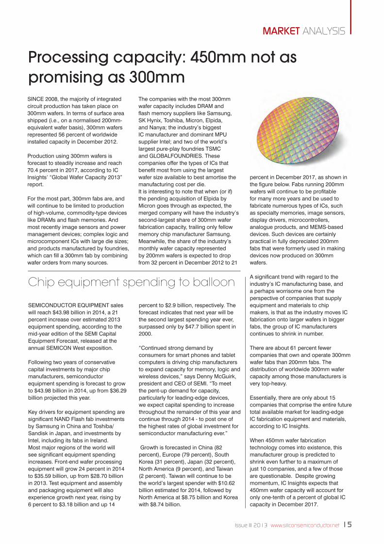
Processing capacity: 450mm not as promising as 300mmSinCE 2008, the majority of integrated circuit production has taken place on 300mm wafers. in terms of surface area shipped (i.e., on a normalised 200mm-equivalent wafer basis), 300mm wafers represented 56 percent of worldwide installed capacity in December 2012.
Production using 300mm wafers is forecast to steadily increase and reach 70.4 percent in 2017, according to iC insights’ “global wafer Capacity 2013” report.
For the most part, 300mm fabs are, and will continue to be limited to production of high-volume, commodity-type devices like DrAMs and flash memories. And most recently image sensors and power management devices; complex logic and microcomponent iCs with large die sizes; and products manufactured by foundries, which can fill a 300mm fab by combining wafer orders from many sources.
The companies with the most 300mm wafer capacity includes DrAM and flash memory suppliers like Samsung, SK Hynix, Toshiba, Micron, Elpida, and nanya; the industry’s biggest iC manufacturer and dominant MPu supplier intel; and two of the world’s largest pure-play foundries TSMC and gLoBALFounDriES. These companies offer the types of iCs that benefit most from using the largest wafer size available to best amortise the manufacturing cost per die.it is interesting to note that when (or if) the pending acquisition of Elpida by Micron goes through as expected, the merged company will have the industry’s second-largest share of 300mm wafer fabrication capacity, trailing only fellow memory chip manufacturer Samsung.Meanwhile, the share of the industry’s monthly wafer capacity represented by 200mm wafers is expected to drop from 32 percent in December 2012 to 21
percent in December 2017, as shown in the figure below. Fabs running 200mm wafers will continue to be profitable for many more years and be used to fabricate numerous types of iCs, such as specialty memories, image sensors, display drivers, microcontrollers, analogue products, and MEMS-based devices. Such devices are certainly practical in fully depreciated 200mm fabs that were formerly used in making devices now produced on 300mm wafers.
A significant trend with regard to the industry’s iC manufacturing base, and a perhaps worrisome one from the perspective of companies that supply equipment and materials to chip makers, is that as the industry moves iC fabrication onto larger wafers in bigger fabs, the group of iC manufacturers continues to shrink in number.
There are about 61 percent fewer companies that own and operate 300mm wafer fabs than 200mm fabs. The distribution of worldwide 300mm wafer capacity among those manufacturers is very top-heavy.
Essentially, there are only about 15 companies that comprise the entire future total available market for leading-edge iC fabrication equipment and materials, according to iC insights.
when 450mm wafer fabrication technology comes into existence, this manufacturer group is predicted to shrink even further to a maximum of just 10 companies, and a few of those are questionable. Despite growing momentum, iC insights expects that 450mm wafer capacity will account for only one-tenth of a percent of global iC capacity in December 2017.
Chip equipment spending to balloon
SEMiConDuCTor EquiPMEnT sales will reach $43.98 billion in 2014, a 21 percent increase over estimated 2013 equipment spending, according to the mid-year edition of the SEMi Capital Equipment Forecast, released at the annual SEMiCon west exposition.
Following two years of conservative capital investments by major chip manufacturers, semiconductor equipment spending is forecast to grow to $43.98 billion in 2014, up from $36.29 billion projected this year.
Key drivers for equipment spending are significant nAnD Flash fab investments by Samsung in China and Toshiba/Sandisk in japan, and investments by intel, including its fabs in ireland. Most major regions of the world will see significant equipment spending increases. Front-end wafer processing equipment will grow 24 percent in 2014 to $35.59 billion, up from $28.70 billion in 2013. Test equipment and assembly and packaging equipment will also experience growth next year, rising by 6 percent to $3.18 billion and up 14
percent to $2.9 billion, respectively. The forecast indicates that next year will be the second largest spending year ever, surpassed only by $47.7 billion spent in 2000.
“Continued strong demand by consumers for smart phones and tablet computers is driving chip manufacturers to expand capacity for memory, logic and wireless devices,” says Denny Mcguirk, president and CEo of SEMi. “To meet the pent-up demand for capacity, particularly for leading-edge devices, we expect capital spending to increase throughout the remainder of this year and continue through 2014 - to post one of the highest rates of global investment for semiconductor manufacturing ever.”
growth is forecasted in China (82 percent), Europe (79 percent), South Korea (31 percent), japan (32 percent), north America (9 percent), and Taiwan (2 percent). Taiwan will continue to be the world’s largest spender with $10.62 billion estimated for 2014, followed by north America at $8.75 billion and Korea with $8.74 billion.
News SiS v1.indd 15 18/07/2013 12:38

16 www.siliconsemiconductor.net Issue III 2013
NEWS ANALYSIS
16 www.siliconsemiconductor.net Issue III 2013
A new method for creating thin films of diamonds could enhance future electronics. In industrial and high-tech settings, diamonds are particularly valued for their hardness, optical clarity, smoothness, and resistance to chemicals, radiation and electrical fields.
For electronics applications, researchers dope diamonds in order to make them conductive, by introducing boron into the diamond manufacturing process.
In the past, it has been a challenge to instil electronic devices with diamond-like qualities by applying a doped diamond coating, or thin film. this is because the high temperatures required to apply a doped diamond thin film would destroy sensitive electronics, including biosensors, semiconductors, and photonic and optical devices.
now, a team of researchers at Advanced diamond technologies, Inc., in Romeoville, Illinois say they have created thin films of boron-doped diamond at temperatures low enough (between 460-600°C) to coat many of these devices. this is described in detail in an Applied Physics Letters paper.
while low-temperature deposition of boron-doped diamond thin films is not conceptually new, the research team found no evidence in the literature of such diamond films that had both sufficient quality and manufacturing rates fast enough to be commercially useful.
tweaking their own normal-temperature boron doping recipe by both lowering the temperature and adjusting the typical ratio of methane to hydrogen gas yielded
a high quality film without appreciable change in conductivity or smoothness compared to diamond films made at higher temperatures. the researchers say more data and study is needed to better understand low-temperature opportunities.
even so, by further optimising the recipe, the researchers expect to be able to deposit boron-doped diamond thin films at temperatures even lower than 400° C.
“the lower the deposition temperature, the larger number of electronic device applications we can enable,” points out hongjun Zeng of Advanced diamond technologies, Inc. “that will further expand the product categories for thin, smooth, conductive diamond coatings,” Zeng he adds.
this work is described in detail in the article, “Low temperature Boron doped diamond,” by hongjun Zeng et al in Journal of Applied Physics Letters, 102, 223108 (2013). http://dx.doi.org/10.1063/1.4809671
Diamonds could make future electronics sparkleApplying thin film diamond coatings at lower temperatures expands the options for electronic devices.
News Analysis v1.indd 16 18/07/2013 12:39
Issue III 2013 www.siliconsemiconductor.net 17
NEWS ANALYSIS
Issue III 2013 www.siliconsemiconductor.net 17
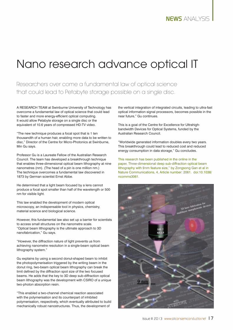
A ReseARCh teAm at swinburne University of technology has overcome a fundamental law of optical science that could lead to faster and more energy-efficient optical computing.It would allow Petabyte storage on a single disc or the equivalent of 10.6 years of compressed hd-tV video.
“the new technique produces a focal spot that is 1 ten thousandth of a human hair, enabling more data to be written to disc,” director of the Centre for micro-Photonics at swinburne, min Gu says.
Professor Gu is a Laureate Fellow of the Australian Research Council. the team has developed a breakthrough technique that enables three-dimensional optical beam lithography at nine nanometres (nm). (the head of a pin is one million nm.)the technique overcomes a fundamental law discovered in 1873 by German scientist ernst Abbe.
he determined that a light beam focused by a lens cannot produce a focal spot smaller than half of the wavelength or 500 nm for visible light.
this law enabled the development of modern optical microscopy, an indispensable tool in physics, chemistry, material science and biological science.
however, this fundamental law also set up a barrier for scientists to access small structures on the nanometre scale.“optical beam lithography is the ultimate approach to 3d nanofabrication,” Gu says.
“however, the diffraction nature of light prevents us from achieving nanometre resolution in a single-beam optical beam lithography system.”
Gu explains by using a second donut-shaped beam to inhibit the photopolymerisation triggered by the writing beam in the donut ring, two-beam optical beam lithography can break the limit defined by the diffraction spot size of the two focused beams. he adds that the key to 3d deep sub-diffraction optical beam lithography was the development with CsIRo of a unique two-photon absorption resin.
“this enabled a two-channel chemical reaction associated with the polymerisation and its counterpart of inhibited polymerisation, respectively, which eventually attributed to build mechanically robust nanostructures. thus, the development of
the vertical integration of integrated circuits, leading to ultra-fast optical information signal processors, becomes possible in the near future,” Gu continues.
this is a goal of the Centre for excellence for Ultrahigh-bandwidth devices for optical systems, funded by the Australian Research Council.
“worldwide generated information doubles every two years. this breakthrough could lead to reduced cost and reduced energy consumption in data storage,” Gu concludes.
this research has been published in the online in the paper, three-dimensional deep sub-diffraction optical beam lithography with 9 nm feature size,” by Zongsong Gan et al in nature Communications, 4, Article number: 2061. doi:10.1038/ncomms3061.
Nano research advance optical IT
Researchers over come a fundamental law of optical science that could lead to Petabyte storage possible on a single disc.
News Analysis v1.indd 17 18/07/2013 12:39
18 www.siliconsemiconductor.net Issue III 2013
NEWS ANALYSIS
18 www.siliconsemiconductor.net Issue III 2013
FoR deCAdes, electronic devices have been getting smaller. It’s now possible - even routine - to place millions of transistors on a single silicon chip. But transistors based on semiconductors can only get so small. “At the rate the current technology is progressing, in 10 or 20 years, they won’t be able to get any smaller,” notes physicist Yoke Khin Yap of michigan technological University. “Also, semiconductors have another disadvantage: they waste a lot of energy in the form of heat.”
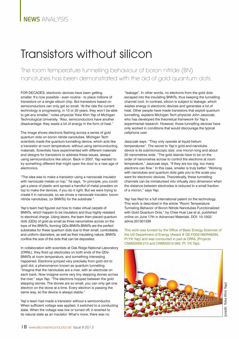
the image shows electrons flashing across a series of gold quantum dots on boron nitride nanotubes. michigan tech scientists made the quantum-tunnelling device, which acts like a transistor at room temperature, without using semiconducting materials. scientists have experimented with different materials and designs for transistors to address these issues, always using semiconductors like silicon. Back in 2007, Yap wanted to try something different that might open the door to a new age of electronics.
“the idea was to make a transistor using a nanoscale insulator with nanoscale metals on top,” he says. “In principle, you could get a piece of plastic and spread a handful of metal powders on top to make the devices, if you do it right. But we were trying to create it in nanoscale, so we chose a nanoscale insulator, boron nitride nanotubes, (or Bnnts) for the substrate.”
Yap’s team had figured out how to make virtual carpets of Bnnts, which happen to be insulators and thus highly resistant to electrical charge. Using lasers, the team then placed quantum dots (Qds) of gold as small as three nanometres across on the tops of the Bnnts, forming Qds-Bnnts.Bnnts are the perfect substrates for these quantum dots due to their small, controllable, and uniform diameters, as well as their insulating nature. Bnnts confine the size of the dots that can be deposited.
In collaboration with scientists at oak Ridge national Laboratory (oRnL), they fired up electrodes on both ends of the Qds-Bnnts at room temperature, and something interesting happened. electrons jumped very precisely from gold dot to gold dot, a phenomenon known as quantum tunnelling.“Imagine that the nanotubes are a river, with an electrode on each bank. now imagine some very tiny stepping stones across the river,” says Yap. “the electrons hopped between the gold stepping stones. the stones are so small, you can only get one electron on the stone at a time. every electron is passing the same way, so the device is always stable.”
Yap’s team had made a transistor without a semiconductor. when sufficient voltage was applied, it switched to a conducting state. when the voltage was low or turned off, it reverted to its natural state as an insulator. what’s more, there was no
“leakage”. In other words, no electrons from the gold dots escaped into the insulating Bnnts, thus keeping the tunnelling channel cool. In contrast, silicon is subject to leakage, which wastes energy in electronic devices and generates a lot of heat. other people have made transistors that exploit quantum tunnelling, explains michigan tech physicist John Jaszczak, who has developed the theoretical framework for Yap’s experimental research. however, those tunnelling devices have only worked in conditions that would discourage the typical cellphone user.
Jaszczak says, “they only operate at liquid-helium temperatures”. the secret to Yap’s gold-and-nanotube device is its submicroscopic size: one micron long and about 20 nanometres wide. ”the gold islands have to be on the order of nanometres across to control the electrons at room temperature,” Jaszczak says. “If they are too big, too many electrons can flow.” In this case, smaller is truly better: “working with nanotubes and quantum dots gets you to the scale you want for electronic devices. theoretically, these tunnelling channels can be miniaturised into virtually zero dimension when the distance between electrodes is reduced to a small fraction of a micron,” says Yap.
Yap has filed for a full international patent on the technology. this work is described in the article “Room temperature tunneling Behavior of Boron nitride nanotubes Functionalized with Gold Quantum dots,” by Chee huei Lee et al, published online on June 17th in Advanced materials. doI: 10.1002/adma.201301339
this work was funded by the office of Basic energy sciences of the Us department of energy (Award # de-FG02-06eR46294, PI:Y.K.Yap) and was conducted in part at oRnL (Projects Cnms2009-213 and Cnms2012-083, PI: Y.K.Yap).
Transistors without siliconThe room temperature tunnelling behaviour of boron nitride (BN) nanotubes has been demonstrated with the aid of gold quantum dots.
(cre
dit:
Yoke
Khi
n Ya
p)
News Analysis v1.indd 18 18/07/2013 12:39

Issue III 2013 www.siliconsemiconductor.net 19
NEWS ANALYSIS
Issue III 2013 www.siliconsemiconductor.net 19
new teChnoLoGY under development at the ohio state University is paving the way for low-cost electronic devices that work in direct contact with living tissue inside the body.
the first planned use of the technology is a sensor that will detect the very early stages of organ transplant rejection.Paul Berger, professor of electrical and computer engineering and physics at ohio state, explains that one barrier to the development of implantable sensors is that most existing electronics are based on silicon, and electrolytes in the body interfere with the electrical signals in silicon circuits. other, more exotic semiconductors might work in the body, but they are more expensive and harder to manufacture.
“silicon is relatively cheap… it’s non-toxic,” Berger says. “the challenge is to bridge the gap between the affordable, silicon-based electronics we already know how to build, and the electrochemical systems of the human body.”
In a paper in the journal electronics Letters, Berger and his colleagues describe a new, patent-pending coating that that they believe will bridge that gap.
In tests, silicon circuits that had been coated with the technology continued to function, even after 24 hours of immersion in a solution that mimicked typical body chemistry.
the photo at the top of this story shows a silicon circuit, coated with a protective layer and immersed in fluid that mimics human body chemistry. this photo is courtesy of ohio state University.
the project began when Berger talked to researchers in ohio state’s department of Biomedical engineering, who wanted to build an insertable sensor to detect the presence of proteins that mark the first signs of organ rejection in the body.
beginning to reject a transplanted organ. doctors would insert a needle into the patient’s body near the site of the implanted organ.
silicon sensors on the needle would detect the protein, and doctors would know how to tailor the patient’s dosage of anti-rejection drugs based on the sensor readings.
Berger believes this work is the first step towards fabricating devices that could be implanted in the body long-term.though the current study describes a silicon sensor coated with aluminium oxide, he envisions that other devices could utilise coatings made from other materials such as titanium. such coatings could even be tailored to boost the performance of sensors or other biomedical devices.
In particular, Berger sees a potential use for coated polymer semiconductors that goes beyond sensing chemicals in the body. he suspects that such semiconductors could replace nerves in the body that have been damaged by disease or injury.
“we could replace a damaged nerve with an artificial neuron and restore functionality immediately, and that’s a really exciting possibility,” Berger says.
Berger’s team is working with ohio state researchers tom Rosol, professor of veterinary biosciences, and Phillip Popovich, professor of neuroscience, to explore that possibility.
Coauthors on the electronics Letters paper included former doctoral students Anisha Ramesh, Fang Ren, Patricia Casal and samit Gupta; current doctoral student in biomedical engineering Andrew theiss, and stephen Lee, associate professor of biomedical engineering. the university intends to license this technology for further development
Sensor can signal organ transplant rejection
they were struggling to make a working protein sensor from gallium nitride.
“we already have sensors that would do a great job at detecting these proteins, but they’re made out of silicon. so I wondered if we could come up with a coating that would protect silicon and allow it to function while it directly touched blood, bodily fluids or living tissue,” explains Berger.
In the body, electrolytes such as sodium and potassium control nerves and muscles and maintain hydration. they do this by carrying a positive or negative electric charge that spurs important chemical reactions. But those same charges make the electrolytes attractive to silicon, which will readily absorb them. once inside, the charges alter the electronic behavior of the silicon so that the readings of a sensor can’t be trusted.In the study, Berger’s team tested whether electrolytes could be blocked from entering silicon with a layer of aluminium oxide.
the researchers submerged the coated test sensors in fluid for up to 24 hours, removed them from the solution, and then ran a voltage across them to see if they were working properly. the tests showed that the oxide coating effectively blocked electrolytes from the solution so the sensors remained fully functional.
once developed, a device using this technology could detect certain proteins that the body produces when it’s just
News Analysis v1.indd 19 18/07/2013 12:39

20 www.siliconsemiconductor.net Issue III 2013
NEWS ANALYSIS
20 www.siliconsemiconductor.net Issue III 2013
A teChnIQUe developed several years ago at the national Institute of standards and technology (nIst) for improving optical microscopes has now been applied to monitoring the next generation of computer chip circuit components.It could provide the semiconductor industry with a crucial tool for improving chips for the next decade or more.the technique, called through-Focus scanning optical microscopy (tsom), has now been shown to detect tiny differences in the three-dimensional shapes of circuit components, which until very recently have been essentially two-dimensional objects.
these three-dimensional tri-gate (FinFet) transistors, pictured above, are among the 3-d microchip structures that could be measured using tsom. (this image was courtesy of Intel Corporation).tsom is sensitive to features that are as small as 10 nm across, perhaps smaller, addressing some important industry measurement challenges for the near future for manufacturing process control and helping maintain the viability of optical microscopy in electronics manufacturing.
For decades, computer chips have resembled city maps in which components are essentially flat. But as designers strive to pack more components onto chips, they have reached the same conclusion as city planners: the only direction left to build is upwards.
new generations of chips feature 3-d structures that stack components atop one another, but ensuring these components are all made to the right shapes and sizes requires a whole new dimension, literally, of measurement capability.
“Previously, all we needed to do was show we could accurately measure the width of a line a certain number of nanometres across,” explains nIst’s
Ravikiran Attota. “now, we will need to measure all sides of a three-dimensional structure that has more nooks and crannies than many modern buildings. And the nature of light makes that difficult.”
Part of the trouble is that components now are growing so small that a light beam can’t quite get at them. optical microscopes are normally limited to features larger than about half the wavelength of the light used, about 250 nm for green light.
so microscopists have worked around the issue by lining up a bunch of identical components at regular distances apart and observing how light scatters off the group and fitting the data with optical models to determine the dimensions. But these optical measurements, as currently used in manufacturing, have great difficulty measuring newer 3-d structures.other non-optical methods of imaging such as scanning probe microscopy are expensive and slow, so the nIst team decided to test the abilities of tsom, a technique that Attota played a major role in developing. the method uses a conventional optical microscope, but rather than taking a single image,
it collects 2-d images at different focal positions forming a 3-d data space.
A computer then extracts brightness profiles from these multiple out-of-focus images and uses the differences between them to construct the tsom image.the tsom images it provides are somewhat abstract, but the differences between them are still clear enough to infer minute shape differences in the measured structures - bypassing the use of optical models, which introduce complexities that industry must face.
“our simulation studies show that tsom might measure features as small as 10 nm or smaller, which would be enough for the semiconductor industry for another decade,” Attota says. “And we can look at anything with tsom, not just circuits. It could become useful to any field where 3-d shape analysis of tiny objects is needed.”
more details of this work have been published in the paper, “Critical dimension metrology by through-focus scanning optical microscopy beyond the 22 nm node,” by R. Attota et al in Applied Physics Letters. doI: 10.1063/1.4809512.
NIST 3-D chip imaging could propel computing
News Analysis v1.indd 20 18/07/2013 12:39

13-093
www.lesker.com
In Strength Through Partnership
All Things Vacuum.Divisions: Process Equipment | Materials | Manufacturing | Vacuum MartTM
KJLC® has been an industry leader in the design, manufacturing and distribution of vacuum technology products and services since 1954. Vacuum science is our business.
Dedicated exclusively to silicon semiconductor, compound
semiconductor and solar recruitment
To find the right professionals with the training and experience tailored to your
industry can be difficult
To be the market leader you need the best people working for you
By using semisolarjobs.net you can reach 100,000 industry professionals globally
Find your new recruit today from the lab to the fab to the boardroom through
www.semisolarjobs.net
e: [email protected]: +44 (0) 1923 690200
Supported by
Untitled-2 1 02/08/2013 11:47

22 www.siliconsemiconductor.net Issue III 2013
MATERIALS INNOVATION
22 www.siliconsemiconductor.net Issue III 2013
Laptops could work longer and electric cars could drive farther if it were possible to further increase the capacity of their lithium-ion batteries.
the electrode material has a decisive influence on a battery’s capacity. so far, the negative electrode (or anode), typically consists of graphite, whose layers can store lithium atoms.scientists at the technische Universitaet Muenchen (tUM) have developed a material made of boron and silicon that could smooth the way to systems with higher capacities.
Loading a lithium-ion battery produces lithium atoms that are taken up by the graphite layers of the negative electrode. However, the capacity of graphite is limited to one lithium atom per six carbon atoms. silicon could take up to ten times more lithium. But unfortunately, it strongly expands during this process - which leads to unsolved problems in battery applications.
Looking for an alternative to pure silicon, scientists at the technische Universitaet Muenchen have now synthesised a
novel framework structure consisting of boron and silicon, which could serve as electrode material. similar to the carbon atoms in diamond, the boron and silicon atoms in the novel lithium borosilicide (LiBsi2) are interconnected tetrahedrally. But unlike diamond they also form channels.
“open structures with channels offer in principle the possibility to store and release lithium atoms,” says thomas Fässler, professor at the Institute of Inorganic Chemistry, technische Universitaet Muenchen. “this is an important requirement for the application as anode material for lithium-ion batteries.”
High-pressure synthesisIn the high-pressure laboratory of the Department of Chemistry and Biochemistry at arizona state University, the scientists
Raising battery life with silicon all the rage
A novel tetrahedral structure consisting of boron and silicon, serving as an electrode material in lithium borosilicide (LiBSi2), forms open channels. This offers, in principle, the possibility to store and release lithium atoms, an important requirement for the anode material used for lithium-ion batteries.
News Analysis v1.indd 22 18/07/2013 12:40

Issue III 2013 www.siliconsemiconductor.net 23
MATERIALS INNOVATION
Issue III 2013 www.siliconsemiconductor.net 23
brought the starting materials lithium boride and silicon to reaction. at a pressure of 100,000 atmospheres and temperatures around 900oC, the desired lithium borosilicide formed. “Intuition and extended experimental experience is necessary to find out the proper ratio of starting materials as well as the correct parameters,” says thomas Fässler.
Lithium borosilicide is stable to air and moisture and withstands temperatures up to 800 ° C. since the framework structure of the lithium borosilicide is unique, Fässler and Zeilinger could give a name to their new framework. In honour of their university, they chose the name “tum.”
Next, thomas Fässler and his graduate student Michael Zeilinger want to examine more closely how many lithium
atoms the material can take up and whether it expands during charging. Because of its crystal structure the material is also expected to be very hard, which would make it attractive as a diamond substitute as well.
More details of this research has been published in the paper, “ LiBsi2: a tetrahedral semiconductor Framework from Boron and silicon atoms Bearing Lithium atoms in the Channels,” by M. Zeilinger et al in angewandte Chemie International Edition, 52 (23), p5978-5982. DoI:10.1002/anie.201301540.
the work was funded by the tUM Graduate school, the German Chemical Industry Fund, the German Research Foundation, the swedish Research Council and the National science Foundation, Usa.
News Analysis v1.indd 23 18/07/2013 12:40

24 www.siliconsemiconductor.net Issue III 2013
3D IMAGING
24 www.siliconsemiconductor.net Issue III 2013
FoR tHE FIRst tIME, scientists working at the National Institute of standards and technology (NIst) say they have demonstrated a new type of lens. It bends and focuses ultraviolet (UV) light in such an unusual way that it can create ghostly, 3D images of objects that float in free space. the easy-to-build lens could lead to improved photolithography, nanoscale manipulation and manufacturing, and even high-resolution three-dimensional imaging, as well as a number of as-yet-unimagined applications in a diverse range of fields.
“Conventional lenses only capture two dimensions of a three-dimensional object,” says one of the paper’s co-authors, NIst’s ting Xu. “our flat lens is able to project three-dimensional images of three-dimensional objects that correspond one-to-one with the imaged object.”
an article published in the journal Nature explains that the new lens is formed from a flat slab of metamaterial with special characteristics that cause light to flow backward - a counterintuitive situation in which waves and energy travel in opposite directions, creating a negative refractive index.
Naturally occurring materials such as air or water have a positive refractive index. You can see this when you put a straw into a glass of water and look at it from the side. the straw appears bent and broken as a result of the change in index of refraction between air, which has an index of 1, and water, which has an index of about 1.33. Because the refractive indices are both positive, the portion of the straw immersed in the water appears bent forward with respect to the portion in air.
the negative refractive index of metamaterials causes light entering or exiting the material to bend in a direction opposite to what would occur in almost all other materials. For instance, if we looked at our straw placed in a glass filled with a negative-index material, the immersed portion would appear to bend backwards, completely unlike the way we’re used to light behaving.
In 1967, Russian physicist Victor Veselago described how a material with both negative electric permittivity and negative magnetic permeability would have a negative index of refraction.permittivity is a measure of a material’s response to an applied
Flat lens makes it all the better to see you with
A novel new lens could lead to improved photolithography, nanoscale manipulation and manufacturing and high-resolution 3D imaging
News Analysis v1.indd 24 18/07/2013 12:40

Issue III 2013 www.siliconsemiconductor.net 25
3D IMAGING
Issue III 2013 www.siliconsemiconductor.net 25
electric field, while permeability is a measure of the material’s response to an applied magnetic field.
Veselago reasoned that a material with a refractive index of -1 could be used to make a lens that is flat, as opposed to traditional refractive lenses, which are curved. a flat lens with a refractive index of -1 could be used to directly image three-dimensional objects, projecting a three-dimensional replica into free space. a negative-index flat lens like this has also been predicted to enable the transfer of image details substantially smaller than the wavelength of light and create higher-resolution images than are possible with lenses made of positive-index materials such as glass.
It took over 30 years from Veselago’s prediction for scientists to create a negative-index material in the form of metamaterials, which are engineered on a subwave-length scale. For the past decade, scientists have made metamaterials that work at microwave, infrared and visible wavelengths by fabricating repeating metallic patterns on flat substrates.
However, the smaller the wavelength of light scientists want to manipulate, the smaller these features need to be, which makes fabricating the structures an increasingly difficult task. Until now, making metamaterials that work in the UV has been impossible because it required making structures with features as small as 10 nanometers, or 10 billionths of a metre.
What’s more, because of limitations inherent in their design, metamaterials of this type designed for infrared and visible wavelengths have, so far, been shown to impart a negative index of refraction to light that is traveling only in a certain direction. this makes them hard to use for imaging and other applications that rely on refracted light.
to overcome these problems, researchers working at NIst took inspiration from a theoretical metamaterial design recently
proposed by a group at the FoM Institute for atomic and Molecular physics in Holland. they adapted the design to work in the UV- a frequency range of particular technological interest.according to co-authors Xu, amit agrawal and Henri Lezec, aside from achieving record-short wavelengths, their metamaterial lens is inherently easy to fabricate. It doesn’t rely on nanoscale patterns, but instead is a simple sandwich of alternating nanometre-thick layers of silver and titanium dioxide, the construction of which is routine. and because its unique design consists of a stack of strongly coupled waveguides sustaining backward waves, the metamaterial exhibits a negative index of refraction to incoming light regardless of its angle of travel.
the researchers say this realisation of a Veselago flat lens operating in the UV is the first such demonstration of a flat lens at any frequency beyond the microwave. By using other combinations of materials, it may be possible to make similarly layered metamaterials for use in other parts of the spectrum, including the visible and the infrared.
the metamaterial flat lens achieves its refractive action over a distance of about two wavelengths of UV light, about half a millionth of a metre - a focal length challenging to achieve with conventional refractive optics such as glass lenses. What’s more, transmission through the metamaterial can be turned on and off using higher frequency light as a switch, allowing the flat lens to also act as a shutter with no moving parts.
“our lens will offer other researchers greater flexibility for manipulating UV light at small length scales,” says Lezec. “With its high photon energies, UV light has a myriad of applications, including photochemistry, fluorescence microscopy and semiconductor manufacturing. that, and the fact that our lens is so easy to make, should encourage other researchers to explore its possibilities.”
the new work was performed in collaboration with researchers from the Maryland NanoCentre at the University of Maryland, College park; syracuse University; and the University of British Columbia, Kelowna, Canada.
More details of this work has been published in the paper, “all-angle negative refraction and active flat lensing of ultraviolet light,” by t. Xu et al in Nature, 497, 470–474, published online on May 23rd, 2013. DoI:10.1038/nature12158.
Left: SEM micrograph of a ring-shaped opening in a chromium sheet located on the surface of a flat slab of metamaterial. Right: Optical micrograph of the image projected beyond the slab under UV illumination, demonstrating that the metamaterial slab acts as a flat lens. (Credit: Lezec/NIST)
The ultraviolet (UV) metamaterial formed of alternating nanolayers of silver (green) and titanium dioxide (blue). The metamaterial has an angle-independent negative refractive index, enabling it to act as a flat lens. When illuminated with UV light (purple) a sample object of any shape placed on the flat slab of metamaterial is projected as a three-dimensional image in free space on the other side of the slab. Here a ring-shaped opening in an opaque sheet on the left of the slab is replicated in light on the right
News Analysis v1.indd 25 18/07/2013 12:40
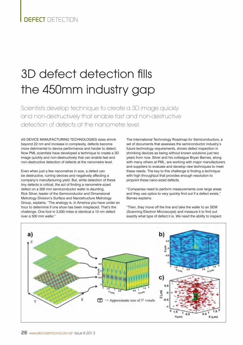
26 www.siliconsemiconductor.net Issue III 2013
DEFECT DETECTION
26 www.siliconsemiconductor.net Issue III 2013
as DEVICE MaNUFaCtURING tECHNoLoGIEs sizes shrink beyond 22 nm and increase in complexity, defects become more detrimental to device performance and harder to detect.Now pML scientists have developed a technique to create a 3D image quickly and non-destructively that can enable fast and non-destructive detection of defects at the nanometre level.
Even when just a few nanometres in size, a defect can be destructive, ruining devices and negatively affecting a company’s manufacturing yield. But, while detection of these tiny defects is critical, the act of finding a nanometre-sized defect on a 300 mm semiconductor wafer is daunting.Rick silver, leader of the semiconductor and Dimensional Metrology Division’s surface and Nanostructure Metrology Group, explains, “the analogy is, in america you have under an hour to determine if one shoe has been misplaced. that’s the challenge. one foot in 3,000 miles is identical a 10 nm defect over a 300 mm wafer.”
the International technology Roadmap for semiconductors, a set of documents that assesses the semiconductor industry’s future technology requirements, shows defect inspection in shrinking devices as being without known solutions just two years from now. silver and his colleague Bryan Barnes, along with many others at pML, are working with major manufacturers and suppliers to evaluate and develop new techniques to meet these needs. the key to this challenge is finding a technique with high throughput that provides enough resolution to pinpoint these nano-sized defects.
“Companies need to perform measurements over large areas and they use optics to very quickly find out if a defect exists,” Barnes explains.
“then, they move off the line and take the wafer to an sEM (scanning Electron Microscope) and measure it to find out exactly what type of defect it is. We need the ability to inspect
3D defect detection fills the 450mm industry gapScientists develop technique to create a 3D image quickly and non-destructively that enable fast and non-destructive detection of defects at the nanometre level.
News Analysis v1.indd 26 18/07/2013 12:40
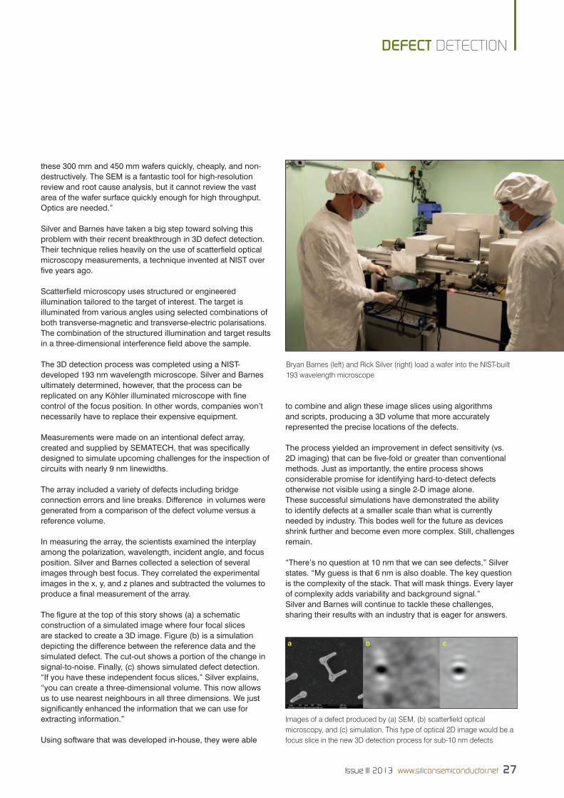
Issue III 2013 www.siliconsemiconductor.net 27
DEFECT DETECTION
Issue III 2013 www.siliconsemiconductor.net 27
these 300 mm and 450 mm wafers quickly, cheaply, and non-destructively. the sEM is a fantastic tool for high-resolution review and root cause analysis, but it cannot review the vast area of the wafer surface quickly enough for high throughput. optics are needed.”
silver and Barnes have taken a big step toward solving this problem with their recent breakthrough in 3D defect detection. their technique relies heavily on the use of scatterfield optical microscopy measurements, a technique invented at NIst over five years ago.
scatterfield microscopy uses structured or engineered illumination tailored to the target of interest. the target is illuminated from various angles using selected combinations of both transverse-magnetic and transverse-electric polarisations. the combination of the structured illumination and target results in a three-dimensional interference field above the sample.
the 3D detection process was completed using a NIst-developed 193 nm wavelength microscope. silver and Barnes ultimately determined, however, that the process can be replicated on any Köhler illuminated microscope with fine control of the focus position. In other words, companies won’t necessarily have to replace their expensive equipment.
Measurements were made on an intentional defect array, created and supplied by sEMatECH, that was specifically designed to simulate upcoming challenges for the inspection of circuits with nearly 9 nm linewidths.
the array included a variety of defects including bridge connection errors and line breaks. Difference in volumes were generated from a comparison of the defect volume versus a reference volume.
In measuring the array, the scientists examined the interplay among the polarization, wavelength, incident angle, and focus position. silver and Barnes collected a selection of several images through best focus. they correlated the experimental images in the x, y, and z planes and subtracted the volumes to produce a final measurement of the array.
the figure at the top of this story shows (a) a schematic construction of a simulated image where four focal slices are stacked to create a 3D image. Figure (b) is a simulation depicting the difference between the reference data and the simulated defect. the cut-out shows a portion of the change in signal-to-noise. Finally, (c) shows simulated defect detection.“If you have these independent focus slices,” silver explains, “you can create a three-dimensional volume. this now allows us to use nearest neighbours in all three dimensions. We just significantly enhanced the information that we can use for extracting information.”
Using software that was developed in-house, they were able
to combine and align these image slices using algorithms and scripts, producing a 3D volume that more accurately represented the precise locations of the defects.
the process yielded an improvement in defect sensitivity (vs. 2D imaging) that can be five-fold or greater than conventional methods. Just as importantly, the entire process shows considerable promise for identifying hard-to-detect defects otherwise not visible using a single 2-D image alone.these successful simulations have demonstrated the ability to identify defects at a smaller scale than what is currently needed by industry. this bodes well for the future as devices shrink further and become even more complex. still, challenges remain.
“there’s no question at 10 nm that we can see defects,” silver states. “My guess is that 6 nm is also doable. the key question is the complexity of the stack. that will mask things. Every layer of complexity adds variability and background signal.”silver and Barnes will continue to tackle these challenges, sharing their results with an industry that is eager for answers.
Images of a defect produced by (a) SEM, (b) scatterfield optical microscopy, and (c) simulation. This type of optical 2D image would be a focus slice in the new 3D detection process for sub-10 nm defects
Bryan Barnes (left) and Rick Silver (right) load a wafer into the NIST-built 193 wavelength microscope
News Analysis v1.indd 27 18/07/2013 12:40

28 www.siliconsemiconductor.net Issue III 2013
EFFICIENCY INTEGRATION
28 www.siliconsemiconductor.net Issue III 2013
BRINGING tHE CoNCEpt of an “artificial leaf” closer to reality, a team of researchers at MIt has published a detailed analysis of all the factors that could limit the efficiency of such a system.the new analysis lays out a roadmap for a research program to improve the efficiency of these systems, and could quickly lead to the production of a practical, inexpensive and commercially viable prototype.
such a system would use sunlight to produce a storable fuel, such as hydrogen, instead of electricity for immediate use. this fuel could then be used on demand to generate electricity through a fuel cell or other device. this process would liberate solar energy for use when the sun isn’t shining, and open up a host of potential new applications.
the new work is described in a recent paper in the proceedings of the National academy of sciences by associate professor of mechanical engineering tonio Buonassisi, former MIt professor Daniel Nocera (now at Harvard University), MIt postdoc Mark Winkler (now at IBM) and former MIt graduate student Casandra Cox (now at Harvard).
It follows up on 2011 research that produced a “proof of concept” of an artificial leaf - a small device that, when placed in a container of water and exposed to sunlight, would produce bubbles of hydrogen and oxygen, as shown below. the device combines two technologies: a standard silicon solar cell, which converts sunlight into electricity, and chemical catalysts applied to each side of the cell. together, these would create an electrochemical device that uses an electric current to
split atoms of hydrogen and oxygen from the water molecules surrounding them.
the goal is to produce an inexpensive, self-contained system that could be built from abundant materials. Nocera has long
Following the crystalline silicon solar-to-fuel roadmap
New analysis by MIT researchers points the way forward to optimising efficiency of an integrated system for harvesting sunlight to make storable fuel.
News Analysis v1.indd 28 18/07/2013 12:40

Issue III 2013 www.siliconsemiconductor.net 29
EFFICIENCY INTEGRATION
Issue III 2013 www.siliconsemiconductor.net 29
advocated such devices as a means of bringing electricity to billions of people, mostly in the developing world, who now have little or no access to it.
“What’s significant is that this paper really describes all this technology that is known, and what to expect if we put it all together,” Cox says. “It points out all the challenges, and then you can experimentally address each challenge separately.”Winkler adds that this is a “pretty robust analysis that looked at what’s the best you could do with market-ready technology.”
the original demonstration leaf, in 2011, had low efficiencies, converting less than 4.7 percent of sunlight into fuel, Buonassis explains. But the team’s new analysis shows that efficiencies of 16 percent or more should now be possible using single-bandgap semiconductors, such as crystalline silicon.
“We were surprised, actually,” Winkler says: Conventional wisdom held that the characteristics of silicon solar cells would severely limit their effectiveness in splitting water, but that turned out not to be the case. “You’ve just got to question the conventional wisdom sometimes,” he says.
the key to obtaining high solar-to-fuel efficiencies is to combine the right solar
cells and catalyst - a matchmaking activity best guided by
a roadmap. the approach presented
by the team allows for each
component of the artificial leaf to be tested individually, then combined.
the voltage produced by a
standard silicon solar cell, about
0.7 volts, is insufficient to power the water-splitting
reaction, which needs more than 1.2 volts. one solution is to
pair multiple solar cells in series. While this leads to some losses at the interface
between the cells, it is a promising direction for the research, Buonassisi says.
an additional source of inefficiency is the water itself - the pathway that the electrons must traverse to complete the electrical circuit - which has resistance to the electrons, says.
Buonassisi. so another way to improve efficiency would be to lower that resistance, perhaps by reducing the distance that ions must travel through the liquid.
“the solution resistance is challenging,” Cox points out. But, she adds, there are “some tricks” that might help to reduce that resistance, such as reducing the distance between the two sides of the reaction by using interleaved plates.
“In our simulations, we have a framework to determine the limits of efficiency” that are possible with such a system, Buonassisi comments. For a system based on conventional silicon solar cells, he says, that limit is about 16 percent; for gallium arsenide cells, a widely touted alternative, the limit rises to 18 percent.Models to determine the theoretical limits of a given system often lead researchers to pursue the development of new systems that approach those limits, Buonassisi says. “It’s usually from these kinds of models that someone gets the courage to go ahead and make the improvements,” he adds.“some of the most impactful papers are ones that identify a performance limit,” notes Buonassisi. But, he adds that there’s a “dose of humility” in looking back at some earlier projections for the limits of solar-cell efficiency: some of those predicted “limits” have already been exceeded.
“We don’t always get it right,” acknowledges Buonassisi, but such an analysis “lays a roadmap for development and identifies a few ‘levers’ that can be worked on.”
this work was supported by the National science Foundation, the air Force office of scientific Research, the singapore National Research Foundation through the singapore-MIt alliance for Research and technology, and the Chesonis Family Foundation.
News Analysis v1.indd 29 18/07/2013 12:40

30 www.siliconsemiconductor.net Issue III 2013
TEST PERFORMANCE
Semiconductor manufacturers use electronic testing to detect devices that do not work and to grade the performance of devices that do work. the testing is performed by testers that use flexible, needle like probes, precisely positioned on a probe card, to contact test pads on each circuit, usually after wafer fabrication is complete but before the wafer is cut into separate die. in recent years the number of contacts per circuit and the number of circuits tested simultaneously have both grown dramatically as circuits have become more complex and manufacturers have sought to increase the speed of the testing process.
the net result is a dramatic increase in the number of probes per card and a concomitant increase in the aggregate force that must be applied to the probe card in order to ensure good electrical contact between each probe and test pad. Some current generation probers can test thousands of devices using tens of thousands of probes with total probe forces adding up to hundreds of kilograms. Forces of this magnitude can easily cause systematic deflections large enough to significantly affect the position of the probes relative to the test pads (Fig 1), particularly in
Approaches for reducing the cost of high pin count probe card test
The cost of high pin count probe card testing can be reduced significantly by eliminating the requirement that cards be tested under conditions that emulate the high mechanical loads they are subjected to in use. In most cases, no-load measurements can provide all the information needed. John Strom, Principal Engineer, Rudolph Technologies, Inc. tells us how.
the Z direction which determines the contact force and the scrubbing motion required to ensure good electrical contact. test engineers use probe card analyzers (PcA) to monitor the position and condition of the probe tips and maintain the performance of the testing process. test equipment manufacturers have responded to the increasing probe forces by increasing the mechanical stiffness of their systems to reduce deflection, further escalating the cost of testing.
PcA manufacturers have followed suit in the belief that accurate probe card analysis requires testing under full load conditions that emulate the test cell, adding to the cost of probe card analysis as well. For full wafer probe cards with large X, Y dimensions, where some bowing of the card may occur under load, the use of a PcA designed to emulate loads on full wafers (ProbeWorx PcA, rudolph technologies, uSA) gives the most accurate measurements. But for the majority of probe cards, card bowing is negligible, and most deflection is linear and occurs in the PcA and probe card interface (Pci). in these cases, no-load testing is a much less expensive approach to probe card analysis and it still provides all the information needed to monitor and maintain probe
Figure 1. As pin counts increase, so do loads exerted on the measurement system, causing deflections that impact probe planarity and alignment measurements
Rudolph v2.indd 30 01/08/2013 12:15

Issue III 2013 www.siliconsemiconductor.net 31
TEST PERFORMANCE
card performance. the discussion below pertains primarily to these applications (where probe card deformation is negligible) using an analyzer such as the PrecisionWorx VX4 System (rudolph technologies, uSA).
Probes are arranged on the probe card to coincide with the positions of probe pads on the device under test. typically, the card is held stationary over a wafer composed of many devices while the wafer is aligned with the probes and moved up to make contact between the probes on the card and probe pads on the device. each probe is flexible and configured so that, as the wafer continues to travel up after initial contact (over-travel), the force exerted by the probe on the pad increases and the probe tip “scrubs” across the pad surface, breaking through any surface contamination to provide good electrical contact.
Planarity measurementsProbe cards must be inspected and serviced regularly to ensure the probe tips are positioned accurately in the Z dimension, to ensure an adequate scrubbing motion, and in X and Y directions, to ensure contact within the probe pad. Z position is usually measured as planarity, the Z deviation of the probe tips from some reference plane, such as the best fit plane of all probes on the card. X and Y positions are measured as alignment. to measure planarity under load, the probe card is held stationary over a flat conductive plate and the plate is moved upward to establish contact (Fig 2). As the plate moves up probes are monitored to determine the Z position of the plate when each probe first makes electrical contact.
the distance traveled by the plate between first and last contacts establishes the range of deviations from perfect planarity. Because the system holding the probe card, consisting of the probe card interface (Pci) and the PcA, is not perfectly stiff, the probe card will move upward as more probes contact the test plate and the forces accumulate. this deflection introduces error in the planarity, stretching the measured range (Fig 3). the conventional approach to eliminating this error has been to increase the stiffness of the Pci/PcA, dramatically increasing the cost of the measurement.
no load measurements use optical or physical methods to measure the position of each probe individually without exerting significant force on the probe card. Although this type of measurement is not new, engineers have assumed that it does not accurately reflect the behavior of the probe card when subjected to high loads in use. careful analysis of the measurement process
now suggests otherwise. When a probe tip scrubs the surface of a pad it leaves a visible scrub mark. the mark is the only physical evidence left by the probe/pad contact, and it is widely used to evaluate many aspects of the probing process, including alignment and over-travel. the scrub ratio relates the length of the scrub mark to the over-travel distance. For instance, a 50% scrub ratio means that 10 µm of over-travel will leave a scrub mark 5 µm long.
consider the scrub marks left by two neighboring probes with a 10 µm difference in Z position during a fully loaded planarity measurement (Fig 4). in a perfectly stiff system (zero deflection), and assuming a 50% scrub ratio, the probe mark left by the lower probe should be 5 µm longer than the mark left by the higher probe. the mark from the lower probe begins when it makes first contact with the pad. After an additional 10 µm of over-travel, when the higher probe makes first contact, the mark from the lower probe is already 5 µm
Figure 2. No-load planarity measurements are made optically, one probe at a time - no force is exerted on the card and there is no deflection of the system. To make loaded planarity measurements a conductive plate is raised toward the probes and the position of the plate is recorded at the time it contacts each probe. As the plate travels up, the number of probes contacting it, and the force opposing its continued travel, increases, eventually causing deflection in the system. The magnitude of the deflection, which is unknown, must be subtracted from the programmed over-travel to determine the actual over-travel applied to the probes
Figure 3. System deflection increases the range of the loaded planarity measurement compared to the unloaded planarity measurement. The X-axis reflects the number of probes contacting the measurement plate, from first contact to last contact. The Y axis is the position of the plate (programmed over-travel) at the time of contact
Rudolph v2.indd 31 01/08/2013 12:15
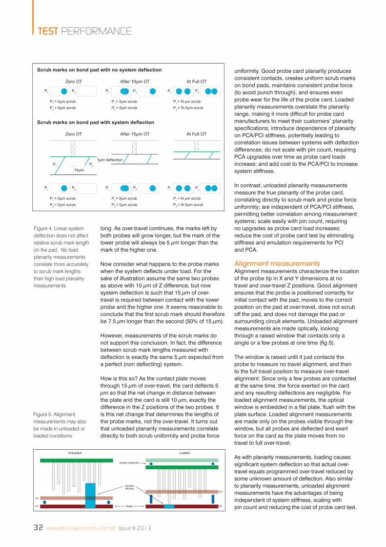
32 www.siliconsemiconductor.net Issue III 2013
TEST PERFORMANCE
long. As over-travel continues, the marks left by both probes will grow longer, but the mark of the lower probe will always be 5 µm longer than the mark of the higher one.
now consider what happens to the probe marks when the system deflects under load. For the sake of illustration assume the same two probes as above with 10 µm of Z difference, but now system deflection is such that 15 µm of over-travel is required between contact with the lower probe and the higher one. it seems reasonable to conclude that the first scrub mark should therefore be 7.5 µm longer than the second (50% of 15 µm).
However, measurements of the scrub marks do not support this conclusion. in fact, the difference between scrub mark lengths measured with deflection is exactly the same 5 µm expected from a perfect (non deflecting) system.
How is this so? As the contact plate moves through 15 µm of over-travel, the card deflects 5 µm so that the net change in distance between the plate and the card is still 10 µm, exactly the difference in the Z positions of the two probes. it is this net change that determines the lengths of the probe marks, not the over-travel. it turns out that unloaded planarity measurements correlate directly to both scrub uniformity and probe force
uniformity. Good probe card planarity produces consistent contacts, creates uniform scrub marks on bond pads, maintains consistent probe force (to avoid punch through), and ensures even probe wear for the life of the probe card. Loaded planarity measurements overstate the planarity range, making it more difficult for probe card manufacturers to meet their customers’ planarity specifications; introduce dependence of planarity on PcA/Pci stiffness, potentially leading to correlation issues between systems with deflection differences; do not scale with pin count, requiring PcA upgrades over time as probe card loads increase; and add cost to the PcA/Pci to increase system stiffness.
in contrast, unloaded planarity measurements measure the true planarity of the probe card, correlating directly to scrub mark and probe force uniformity; are independent of PcA/Pci stiffness, permitting better correlation among measurement systems; scale easily with pin count, requiring no upgrades as probe card load increases; reduce the cost of probe card test by eliminating stiffness and emulation requirements for Pci and PcA.
Alignment measurementsAlignment measurements characterize the location of the probe tip in X and Y dimensions at no travel and over-travel Z positions. Good alignment ensures that the probe is positioned correctly for initial contact with the pad, moves to the correct position on the pad at over-travel, does not scrub off the pad, and does not damage the pad or surrounding circuit elements. unloaded alignment measurements are made optically, looking through a raised window that contacts only a single or a few probes at one time (fig 5).
the window is raised until it just contacts the probe to measure no travel alignment, and then to the full travel position to measure over-travel alignment. Since only a few probes are contacted at the same time, the force exerted on the card and any resulting deflections are negligible. For loaded alignment measurements, the optical window is embedded in a flat plate, flush with the plate surface. Loaded alignment measurements are made only on the probes visible through the window, but all probes are deflected and exert force on the card as the plate moves from no travel to full over-travel. As with planarity measurements, loading causes significant system deflection so that actual over-travel equals programmed over-travel reduced by some unknown amount of deflection. Also similar to planarity measurements, unloaded alignment measurements have the advantages of being independent of system stiffness, scaling with pin count and reducing the cost of probe card test.
Figure 4. Linear system deflection does not affect relative scrub mark length on the pad. No load planarity measurements correlate more accurately to scrub mark lengths than high load planarity measurements
Figure 5. Alignment measurements may also be made in unloaded or loaded conditions
Rudolph v2.indd 32 01/08/2013 12:15

Issue III 2013 www.siliconsemiconductor.net 33
TEST PERFORMANCE
Test strategies and PCI designCurrently the industry standard is high load measurements using an emulating PCI, even though the accuracy of the emulation is often unknown. A simplified PCI designed for unloaded planarity and alignment measurements is much simpler to design and produce (Fig 6).
In addition to eliminating the cost of increased stiffness, unloaded measurements with the simplified PCI relax the requirements for parallelism between the probe card and the PCA, and permit further cost reductions through electrical simplifications, such as the use of a PCA with fewer channels and a heavily bussed PCI. ConclusionThe cost of probe card testing is being driven upward by the need to design stiffer systems to resist deflections caused by the increasing number of probes on each card. Customers are responding with demands that PCA manufacturers reduce the cost of probe card testing. These costs can be significantly reduced by using no-load testing.
The work summarized here demonstrates that no load testing using appropriately simplified PCI designs provides all the information needed to evaluate probe planarity and alignment. In fact, unloaded measurements can provide
Figure 6 An emulating (loaded) PCI (bottom left) is compared to a simplified (no load) PCI (bottom right). The top plot compares loaded planarity measurements made with an emulating and a simplified PCI - the stretching effects of deflection are apparent. The middle plot compares no-load planarity measurements made with an emulating and a simplified PCI - the stretching effect is absent. The lower plot compares unloaded alignment measurements made with an emulating and a simplified PCI - again the measurements correlate well
more meaningful information about probe card performance in a test cell than loaded measurements. The trend toward more probes per card is likely to continue. Unloaded measurements eliminate the need to modify the PCA system changes as probe card loads increase.
© 2013 Angel Business Communications.Permission required.
Rudolph v3.indd 33 02/08/2013 11:49

34 www.siliconsemiconductor.net Issue III 2013
NEW PRODUCTS SHOW REVEALS
New products and technologies revealed for 2013
With SEMICON West behind us for another year, many of the majorplayers used this opportunity to show case the latest in product and
technology offerings. Here are a few of them.
Robot automated transportation for cleanrooms revealedRotH & Rau - oRtneR, a factory automation specialist, and its partner metralabs automation, a provider of freely navigating autonomous mobile robots, have introduced their jointly-developed mobile robot, SCout at SemiCon West. SCout has been specially developed for the fl exible and automated transportation of materials in semiconductor fabs and other clean production environments.
SCout navigates autonomously, without any kind of guidance system and communicates via WiFi and operator Gui to issue new transport jobs and show important status information like its current position. the robot is cleanroom suitable up to iSo class 3 / uS Fed class 1 and has more than 5,000 km of autonomous navigation in clean rooms, which proves its reliability.
“thanks to its compact size and reliable sensor technology, SCout can be used safely in areas where people and machines work closely together,”
explains matthias merten, Ceo of metralabs automation, inc. “this makes SCout an ideal alternative in cases where a permanently installed transport system such as a rail or a conveyor system cannot be implemented or would be too expensive. SCout is capable of transporting various materials and products between any point in the fab, taking measurements, providing tools and auxiliaries. Various attachments like mechanical manipulators (e.g. robot arms or linear axis) and transportation trays (e.g. for the transportation of four
SmiF pods or Ha200 storage boxes) enable SCout to be adjusted to different conditions according to the desired use.
“SCout is an integral part of our “missing link” concept, which covers custom-tailored automation solutions for existing semiconductor fabs. these solutions are primarily directed at semi-automated production lines with high requirements for personnel because they can cut costs dramatically by minimising downtime and freeing up manpower,” adds Karli Hantzschmann, division manager automation of Roth & Rau - ortner.
older wafer fabrication businesses often called for cassettes to be handled manually between the production processes. this tied up valuable assets, such as staff; required high investments in time and cost and was prone to error. ortner’s solution replaces formerly manual links between two work steps, improving the process for transportation, tool loading, storage and identifi cation.
SenSiRion’S new Slq-qt500 features a fl ow range up to 120 ml/min for water-based liquids as well as hydrocarbon based liquids. it is suited for the integration into demanding coating systems in the semiconductor industry.applications include high-end semiconductor process control, industrial automation and fast dosing operations.
Based on Sensirion’s thermal microsensor technology, the wetted parts are the pFa fi ttings and the quartz
glass tube. the whole fl uidic path is straight and there are no obstacles or moving parts in the sensor.
Sensiron says its Slq-qt500 is ideally suited for liquids with virtually any viscosity as well as liquids which contain small particles as long as they are not abrasive in the quartz glass
tube. a smart digital interface and RS485 communication is offered for long distance and bus capabilities. the fi rm believes the sensitivity and measuring speed offer new possibilities for the monitoring or control of fast dosing operations.
the instantaneous fl ow rate of the fl uid is available as well the output of a total dosed volume with automatic dosing detection. the sensor is available with calibration for H2o and isopropanol (ipa).
Sensirion unveils fl exible fl ow sensor
New Products v1.indd 34 18/07/2013 12:41
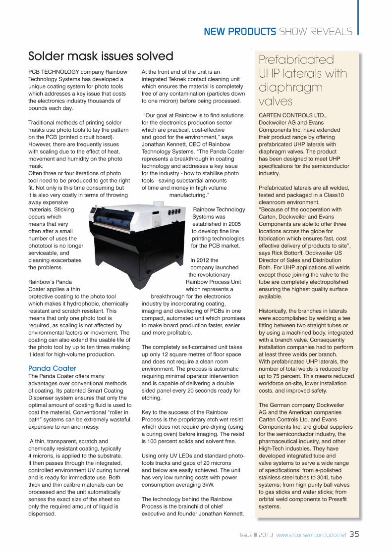
Issue III 2013 www.siliconsemiconductor.net 35
NEW PRODUCTS SHOW REVEALS
Solder mask issues solvedpCB teCHnoloGY company Rainbow technology Systems has developed a unique coating system for photo tools which addresses a key issue that costs the electronics industry thousands of pounds each day.
traditional methods of printing solder masks use photo tools to lay the pattern on the pCB (printed circuit board). However, there are frequently issues with scaling due to the effect of heat, movement and humidity on the photo mask. often three or four iterations of photo tool need to be produced to get the right fi t. not only is this time consuming but it is also very costly in terms of throwing away expensive materials. Sticking occurs which means that very often after a small number of uses the phototool is no longer serviceable, and cleaning exacerbates the problems.
Rainbow’s panda Coater applies a thin protective coating to the photo tool which makes it hydrophobic, chemically resistant and scratch resistant. this means that only one photo tool is required, as scaling is not affected by environmental factors or movement. the coating can also extend the usable life of the photo tool by up to ten times making it ideal for high-volume production.
Panda Coaterthe panda Coater offers many advantages over conventional methods of coating. its patented Smart Coating dispenser system ensures that only the optimal amount of coating fl uid is used to coat the material. Conventional “roller in bath” systems can be extremely wasteful, expensive to run and messy.
a thin, transparent, scratch and chemically resistant coating, typically 4 microns, is applied to the substrate. it then passes through the integrated, controlled environment uV curing tunnel and is ready for immediate use. Both thick and thin calibre materials can be processed and the unit automatically senses the exact size of the sheet so only the required amount of liquid is dispensed.
at the front end of the unit is an integrated teknek contact cleaning unit which ensures the material is completely free of any contamination (particles down to one micron) before being processed.
“our goal at Rainbow is to fi nd solutions for the electronics production sector which are practical, cost-effective and good for the environment,” says Jonathan Kennett, Ceo of Rainbow technology Systems. “the panda Coater represents a breakthrough in coating technology and addresses a key issue for the industry - how to stabilise photo tools - saving substantial amounts of time and money in high volume
manufacturing.”
Rainbow technology Systems was established in 2005 to develop fi ne line printing technologies for the pCB market.
in 2012 the company launched
the revolutionary Rainbow process unit which represents a
breakthrough for the electronics industry by incorporating coating, imaging and developing of pCBs in one compact, automated unit which promises to make board production faster, easier and more profi table.
the completely self-contained unit takes up only 12 square metres of fl oor space and does not require a clean room environment. the process is automatic requiring minimal operator intervention and is capable of delivering a double sided panel every 20 seconds ready for etching.
Key to the success of the Rainbow process is the proprietary etch wet resist which does not require pre-drying (using a curing oven) before imaging. the resist is 100 percent solids and solvent free.
using only uV leds and standard photo-tools tracks and gaps of 20 microns and below are easily achieved. the unit has very low running costs with power consumption averaging 3kW.
the technology behind the Rainbow process is the brainchild of chief executive and founder Jonathan Kennett.
Prefabricated UHP laterals with diaphragm valvesCaRten ContRolS ltd., dockweiler aG and evans Components inc. have extended their product range by offering prefabricated uHp laterals with diaphragm valves. the product has been designed to meet uHp specifi cations for the semiconductor industry.
prefabricated laterals are all welded, tested and packaged in a Class10 cleanroom environment. “Because of the cooperation with Carten, dockweiler and evans Components are able to offer three locations across the globe for fabrication which ensures fast, cost effective delivery of products to site”, says Rick Bottorff, dockweiler uS director of Sales and distribution Both. For uHp applications all welds except those joining the valve to the tube are completely electropolished ensuring the highest quality surface available.
Historically, the branches in laterals were accomplished by welding a tee fi tting between two straight tubes or by using a machined body, integrated with a branch valve. Consequently installation companies had to perform at least three welds per branch. With prefabricated uHp laterals, the number of total welds is reduced by up to 75 percent. this means reduced workforce on-site, lower installation costs, and improved safety.
the German company dockweiler aG and the american companies Carten Controls ltd. and evans Components inc. are global suppliers for the semiconductor industry, the pharmaceutical industry, and other High-tech industries. they have developed integrated tube and valve systems to serve a wide range of specifi cations: from e-polished stainless steel tubes to 304l tube systems; from high purity ball valves to gas sticks and water sticks; from orbital weld components to pressfi t systems.
New Products v1.indd 35 18/07/2013 12:41

36 www.siliconsemiconductor.net Issue III 2013
NEW PRODUCTS SHOW REVEALS
Solid State equipment llC (SSeC), has introduced its Waferetch and WaferStorm product lines. these platforms are specifically configured to meet the process needs of applications in advanced packaging, memS, and compound semiconductor manufacturing. the firm’s latest tools aim to improve process control and reduce chemistry consumption, translating to higher throughput and lower cost of ownership (Coo).
one key Coo reduction driver was enabled by an engineering break-through that makes the chambers more compact and stackable. this results in 50 percent more process chambers within the same small footprint of the firm’s legacy products. the Waferetch platform (below) is configured for aqueous-based etch processes such as through-silicon via (tSV) reveal. the WaferStorm platform is configured for solvent-based processes such as resist strip, metal lift-off and tSV cleaning.
“Superior performance, improved yields, and increased throughput at a lower Coo are the cornerstones of SSeC’s single wafer wet processing approach,” says laura Rothman mauer, Chief technical officer of Solid State equipment llC.She adds,
WaferEtchthe Waferetch platform is an aqueous-based, customisable platform, uniquely configured to meet the needs of specific etch applications for 3d iCs, memS and compound semiconductor processes. these systems use a wet etch process chemistry that demonstrates optimal etch rate and in situ cleaning.
SSEC unveils single wafer wet processing tools
the flagship of the Waferetch platform, the tSV ReVealeR, is specifically configured to address the requirements of tSV reveal, which is the process where the backside of the wafer is thinned to reveal the copper interconnects. it has become a target area in the manufacture of 2.5d and 3d iC packaging for process control and cost reduction. WaferEtch TSV REVEALERthe tSV ReVealeR replaces three tools required for the dry etch approach: plasma etch, silicon thickness measurement, and clean. an optical end point detection system with advanced algorithms determines when vias are revealed. integration of a wafer thickness measurement sensor in the etch system provides closed-loop control of the etching process.
WaferStormthe WaferStorm platform (above right) is a solvent-based platform, initially available in three unique configurations: tSV CleaneR, metal liFteR, and dRY Film RemoVeR. all WaferStorm systems are based on SSeC’s unique soak and spray technology, which provides improved performance at lower Coo than conventional wet bench-only or spray-only approaches. the process combines equal soak time in the wet buffer tank for each wafer, followed by spray, and then a final step depending on the process being performed. this unique combination minimizes both spray time and chemistry use, and adds a significant level of process control. the reduction in spray time results in increased throughput.
WaferStorm TSV CLEANERtSV clean is a critical process step that is essential to reliability. the deep reactive ion etch (dRie) process leaves behind a polymer residue which can lead to defects and voids in the barrier, seed, and fill steps that follow. SSeC’s WaferStorm tSV CleaneR is proven to remove residues in high-aspect-ratio holes that wet bench-only or spray-only tools leave behind. the tool features equal-time soak software for process control.
WaferStorm metal liFteRmetal lift-off consists of the sequential steps of photolithography, metal deposition, and solvent lift-off of both
metal and non-metal substances in memS and compound semiconductor applications. the SSeC WaferStorm metal liFteR is configured specifically to perform the sequential soak and spray combinations unique to the process. WaferStorm METAL LIFTERthe immersion station operates in a low-oxygen atmosphere, which maintains the bath longer. Following a soak in the immersion tank, lift-off takes place in a spray station using a high-pressure chemical spray, which translates to increased throughput.
the tool features a lift-off material filtration station and strainers for separating metal films, which results in the complete removal of the metal.
WaferStorm DRY FILM REMOVERRemoval of dry film resists used in advanced microbumping processes for 3d iCs and wafer level packaging (Wlp) applications is a challenge due to the film thickness and composition. the SSeC WaferStorm dRY Film RemoVeR combines heated chemistries and proprietary soak and spray at high pressure for rapid and complete removal of stubborn dry film residue. WaferStorm DRY FILM REMOVERthe soak step uses heated solvents throughout the buffer cycle time. after being softened by the soak, the wafers are transferred to the single-wafer spray station where they are exposed to high-pressure fan sprays with heated solvents for rapid removal of dry film residue. this combination ensures thorough removal and increased throughput.
New Products v1.indd 36 18/07/2013 12:41

Issue III 2013 www.siliconsemiconductor.net 37
NEW PRODUCTS SHOW REVEALS
eV GRoup (eVG), a supplier of wafer bonding and lithography equipment for the memS, nanotechnology and semiconductor markets, has introduced the latest version of its eVG 40nt automated measurement system. the tool, pictured above, is designed to work in concert with the company’s Gemini FB fusion wafer bonding system to support the manufacture of next-generation 3d-integrated CmoS image sensors.
the enhanced eVG40nt measures wafer-to-wafer alignment accuracy to within 40 nm (3 sigma), while its seamless software integration with the Gemini FB provides a closed-loop fusion bonding control system that enables the manufacture of ultra-fi ne-pitch (less than two micron) through-silicon vias (tSVs).these tighter specifi cations are necessary for enabling the production of 3d-integrated image sensors, and pave the way for accelerating 3d-integration with other device types, such as stacked memory.
“eV Group’s Gemini FB fusion wafer bonding platform is the de facto industry standard for CmoS image sensor production, and already leads the industry in wafer-to-wafer alignment accuracy due to our proprietary SmartView alignment technology,” says thorsten matthias, business development director at eV Group.
“the integration of Gemini FB with the enhanced eVG40nt brings statistical process control and alignment accuracy
EV Group tool pushes the limits on 3D ICs
to a whole new level, and pushes 3d-iC manufacturing to new limits.
High-precision manufacturing requires accurate metrology that is seamlessly integrated into the process to enable real-time monitoring and fast corrective action.
in the case of wafer bonding, measuring and mapping each die gives valuable insight into local stress variations created during upstream processes, which can cause distortions and local misalignments further downstream,” he continues.
Fusion wafer bonding is ideally suited for 3d-integrated image sensors and other stacked devices because it is a room-temperature bonding process, which eliminates misalignment due to thermal expansion mismatch between the wafers. Having the ability to inspect the quality of the wafer bond and measure alignment accuracy prior to the fi nal annealing step provides an easy rework path, thereby enabling 100-percent yield for wafer stacking.
the Gemini FB platform combines eVG’s
lowtemp plasma activation technology, wafer cleaning, SmartView wafer-to-wafer alignment and
fusion wafer bonding in
a single fully automated high-volume-manufacturing system.
the eVG40nt performs
highly accurate, non-destructive, top-to-bottom side
alignment accuracy measurements on double-sided structured wafers or bond interfaces, as well as critical dimension and box-in-box measurements of single and double-sided structured wafers.“next-generation image sensors are the technological frontrunners for 3d-iC manufacturing technology,” according to Hermann Waltl, executive sales and customer support director at eV Group. “High-density tSV arrays, sub-micron-diameter tSVs and ultra-thin wafers have all been successfully transferred into high-volume image sensor manufacturing. now that adoption of wafer-to-wafer 3d stacking for image sensors is well underway, we expect to see 3d-integration follow very soon for other devices such as stacked memory.”
eSSemteC, a Swiss manufacturer of production systems for electronic assembly and packaging, has introduced the Scorpion high-speed jetter at SemiCon West.the Scorpion fully automatic jetting system sets new standards in dispensing technology and improves overall equipment effi ciency. absolute throughput is maximized with piezo jetting valves which enable the jetting of fl uids over a wide range of viscosity with speeds of up to 800 Hz.
Wastage of expensive material is minimized with a fl uid box of less than 150 nano liters. there is no tubing to connect the fl uid to the jet valve and hence messy cleaning and maintenance operations are minimized. Setting up new recipes is quick and easy with essemtec’s brand new ediS
software which also offers context sensitive help. point and touch features are intuitive to learn and programming of dots, lines or various shapes is a breeze, while Cad import is also supported. processes are developed in no time thanks to a library of “best known parameters” for a wide range of common fl uids.
the Scorpion is a highly versatile system and can be equipped with up to four valves or pumps, including jet valves, archimedian screw valves, time pressure valves and slider valves to accommodate virtually all applications. these include encapsulation, dam-and-fi ll, underfi l, led cavity, conductive adhesive, solder paste, phosphor silicon cavity fi ll and many more.
Essemtec introduces high speed jetter
New Products v1.indd 37 18/07/2013 12:41

38 www.siliconsemiconductor.net Issue III 2013
NEW PRODUCTS SHOW REVEALS
KLA-Tencor defect analysis on another levelKla-tenCoR CoRpoRation has revealed the new 2910 Series optical wafer defect inspection platform with nanopoint technology and the new edR-7100 electron-beam wafer defect review system.
meeting iC manufacturers’ need for accelerated defect sourcing on advanced devices, these two tools combine increased speed with seamless connectivity to quickly fi nd and identify defects that inhibit yield and reliability.the 2910 Series’ improved defect capture and the edR-7100’s enhanced review resolution have been demonstrated by detecting and imaging unique defects located at the bottom of three-dimensional or vertical pattern structures such as FinFets.
“our customers’ need to quickly ramp processes that use complex patterning strategies creates defect challenges that drive our on going innovation in both optical and electron-beam technologies,” says Bobby Bell, executive vice president of Kla-tencor’s Wafer inspection Group.“We continue to extend optical inspection through novel methods such as our nanopoint technologies. these advances take our 2910 Series tools to a new level of optical defect detection while preserving optical inspection speed. additional developments in e-beam technology allow our edR-7100 to accurately identify extremely tiny defects that are not always visible on other e-beam review tools. pairing these tools provides our customers with an effi cient inspection and review solution for qualifying their leading-edge processes.”
Building on the defect discovery capabilities produced by Kla-tencor’s patented nanopoint technologies, the 2910 Series features new optical apertures and inspection modes that have been shown to provide a substantial
improvement in the capture of several yield-critical defect types, such as voids, bridges and bottom bridges.What’s more, the tools feature a signifi cant increase in throughput over the previous-generation 2900 Series, enabling engineers to sample more wafers or inspect additional process levels for faster identifi cation of yield excursions.
the edR-7100 includes fourth-generation e-beam immersion optics, producing improved resolution and additional review modes for imaging a wide range of defect types, with a particular benefi t being the tool’s ability to locate and identify defects at the bottom of complex pattern features or high-aspect ratio structures.
these technical advances also enable enhanced throughput compared to the edR-7000, allowing engineers to sample additional defects to gain a more accurate understanding of the defect population on the wafer.
Since iC fabs increasingly require e-beam review of un-patterned wafer defects detected by inspectors such as the Surfscan Sp3, the edR-7100 features a new optical microscope and energy-dispersive x-ray (edX) compositional analysis subsystem to aid in the classifi cation and characterization of bare wafer defects.
multiple 2910 Series optical inspection tools, confi gured as either the 2910 or 2915, and edR-7100 e-beam review tools have been installed at leading iC manufacturers where they are being used for new technology development and ramp. in order to help protect a fab’s capital investment, the 2910 Series and the edR-7100 tools are both upgradeable from their predecessors, the 2900 Series and the edR-7000, respectively.
“Smart” pressure transient insensitive MFC can perform self diagnosticsBrooks automation provider of advanced fl ow, pressure, vacuum, level and vapour delivery solutions, has expanded with the introduction of four products and a new technology development centre in irvine, Calif. the new products include the GF135 advanced diagnostic mass fl ow controller (mFC) and three mFCs for high-fl ow applications. these mFCs, which expand Brooks’ GF100 Series product line for semiconductor processing applications, are all built on a common platform and interface, enabling an entire system to use one product platform.
“Brooks continues to provide innovative solutions for the semiconductor industry by expanding its portfolio of advanced technology products,” said Bill Valentine, chief technology offi cer for Brooks instrument. “our strategic focus for the technology centre will be to strengthen our relationships with semiconductor end users and equipment manufacturers so we can translate customer needs into product requirements.” the GF135 delivers game-changing technology because it is the fi rst “smart” pressure transient insensitive (pti) mFC that can perform self diagnostics – including integral rate-of-decay fl ow measurement – without stopping the fl ow of process gas. Semiconductor manufacturers can now verify accuracy, check valve leak-by, and monitor sensor drift in real time without removing the fl ow controller from the gas line. this new diagnostic technology allows for uninterrupted production of wafers and thousands of dollars in potential daily cost savings.
the GF101, GF121 and GF126 are high-fl ow thermal mFCs that are suitable for process engineers in led and semiconductor process and purge applications that require high purity and fl ow rates up to 300 slpm.
New Products v1.indd 38 18/07/2013 12:41

Issue III 2013 www.siliconsemiconductor.net 39
CORPORATE PARTNERS DIRECTORY
Fan Filter Units
Furnaces
Furnaces
Material Processing
Wafers
Vacuum Equipment
Solder Rework Wet Benches
Materials, Processes and Equipment
MFCsLiquid Nitrogen Piping
Automation/Wafer Handling
To promote your Products and Services contact: Shehzad Munshi T: +44 (0)1923 690 215E: [email protected]
39 Corporate Partners v1.indd 39 29/07/2013 16:42

PHOTOLITHOGRAPHYFOR TSV AND 3D-IC
Conformal Coating in Vertical Vias
Exposure with Proximity Lithography
In-Via Resist Development
GET IN TOUCH To Discuss Your Manufacturing Needs: www.EVGroup.com
EVG®150 Resist Processing System Via
pro
cess
ed o
n E
VG
® s
yste
ms
Untitled-1 1 28/03/2013 15:58