apr l bentley, haken, r unclassified l inimmunn
TRANSCRIPT

V .996~ 377 CARNEGIE-MELLON LA4IV PITTSBURGH PA DEPT OF COMPUTER -ETC F/G 9/1STATISTICS ON VLSI DESIGNS. (U)APR 80 J L BENTLEY, 0 HAKEN, R W HON NOOOI-76-C-0370
UNCLASSIFIED CNU-CS-BO-111 L'umminnnmI inimmunn-i'll"-- o
ininuuuuuummflfllfl ED

'y LEVELsStatistics on VLSI Designs-
N Jon Louis- BentleyN Dorothea Haken
Robert W. Hon
Department of Computer Sc ienceCarnegie-Mellon University
Pittsburgh, Pennsylvania 15213
DEPARTMENT E* of
COMPUTER SCIENCE
Carnegie-Mellon UniversityCUM =HM ON STAT~b!w XApprowed for pubfc .asauq
asU.I~j~ 81 ~098

cM-CS-80- Ill
Statistics on VLSI Designs,
Jon Louis Bentley 2
Dorothea Haken
Robert W. Hon
Department of Computer ScienceCarnegie-Mellon University
Pittsburgh, Pennsylvania 15213
17 April 1980
Abstract -- This paper presents a statistical study of the components on VLSI chips. We examine
the size and shape of components, and their placement over the chip area. The data is useful for
building efficient VLSI design tools: the form of the distribution shows that some simple strategies can
lead to efficient algorithms, and the parameters of the distribution aid in choosing program
parameters. To illustrate the application of the statistics to VLSI design tasks, we present an
algorithm for solving the "rectangle intersection" problem that arises in design rule checkers.
This reseorih was Sui!potled in port by the Defense Advancea Research Projects Agency undef ContractF33615-7 ( - 1551 (nioiloied by the Air Force Oftice of Sc ienitfic Re.search) and in pat by Ihe Office of Naval Resnr ach underContract N00014.76-C 0370
2Also with the Depatineiit of Mathematics.

17 April1980 VLSI Statistics I
Table of Contents1. Introduction1
2. Statistics on Designs 2
2.1 Description of the Designs 22.2 Statistics on Shape 3
2.2.1 A Trichotomy of Rectangles 42.2.2 Data on Components 62.2.3 Data on Wires 62.2.4 Data on Other Rectangles7
2.3 Data on Placement 82.4 A Probabilistic Model 9
3. Applications of the Statistics 12
3.1 An Algorithm for Finding Rectangle Intersections 123.2 A Pascal Program 153.3 Applications in VLSI Task~s 17
4. Conclusions 19
References 20
1. Description of the Chips 21
IL. Component Histograms 22
Ill. Wire Histograms 29
IV. Histograms of Other Rectangles 36
V. Placement Histograms 43
V.1 Two-dimensional Histograms 43V.2 One-dimensional Histograms 50
VI. Data on Rectangle Area 57
',n' For

17 April 1980 VLSI Statistics 1
1. IntroductionThe "VLSI explosion" seems to be making the world of computers better and better: with every
technological advance we can build machines that are smaller, faster, and cheaper than their
predecessors. There are, however, several concomitant difficulties associated with these advances,
one of the more noticeable being the problems inherent in designing a chip that contains hundreds of
thousands of transistors. For this reason a great deal of recent research has focussed on building a
VLSI design system that can automate certain design tasks. These tasks include such problems aslaying out components. routing wires between components. and design rule checking to ensure that
the design satisfies a set of constraints.
The primary purpose of this paper is to present a set of statistics on VLSI chips that can be used
when constructing a VLSI design system. The statistics describe the geometry of chips: that is, theJ
shape of their components and how those components are placed on the chip. To illustrate theapplication of the statistics, we will describe an algorithm useful in design rule checking that was
developed by using the statistics. (A design rule checker that uses this algorithm is currently underdevelopment at Carnegie-Mellon.) The primary audience for this paper, therefore, is the community
interested in constructing VLSI design systems.
A secondary purpose of this paper is to provide a study in "applied algorithm design". A great deal
of work has been done recently on the probabilistic analysis of algorithms, and the design of
algorithms with fast expected running time. One weak part of that work, however, is that it has merely
assumed that the input data is drawn from a particular underlying distribution, and has not questioned
how practitioners might justify that assumption. This paper provides an example of the justification of
probabilistic assumptions, and the development of both an abstract algorithm and a concrete
program based on the assumptions.
Chapter 2 contains the statistical study of a set of VLSI designs. An algorithm for computing4rectangle intersections that exploits those statistics to achieve fast expected running time is
presented in Chapter 3. and conclusions are offered in Chapter 4.

17 April 1980 VLSI Statistics -2-
2. Statistics on DesignsIn this chapter we will study the distribution of components on VLSI chips. There are two primary
knowledge sources that we will bring to bear in. this study. The first is an a priori knowledge of the
design style of (at least one school of) chip designers. The second source is an empirical study of a
set of actual chip designs.
This chapter is organized as follows. In Section 2.1 we briefly describe both the basic design
philosophy underlying the chips we studied and the chips themselves. Section 2.2 contains statistics
on the shape of the components placed on chips, and Section 2.3 contains statistics on the
placement of the components on the chips. A probabilistic model summarizing these studies is
presented in Section 2.4. (All the measurements in this chapter are used in the construction of the
rectangle intersection algorithm described in Chapter 3. Since issues of area are not important for
the algorithmn of Chapter 3, we defer discussion of the data on the area occupied by components and
wires to Appendix VI.)
2.1 Description of the DesignsBefore we describe the statistics in detail, it is important to give a few words of background on the
chip designs studied. Ail were the result of VLSI design courses taught at research institutions,including Caltech. Carnegie-Mellon, MIT, Stanford, and Xerox PARC. The designers were
researchers schooled in the Mead and Conway [1980] style of hierarchical IC design; the target
process was silicon-gate nMOS, using Mead and Conway's design rules and a value of A~ from 2.0 to
3.0 microns. (The constant X. is the size of the smallest features resolvable by the implementation
process; typical minimum-sized transistors have gate widths of 2A.) All of the designs were expressed
in a geometric specification language called Caltech Intermediate Format (or COF -- see Hon and
Sequin [ 1980]), regardless of the design system used to lay out the chip.
In this section we will present statistics on sixteen VLSI designs. All designs are taken from recent
multiproject chips managed by the LSl group at Xercx PARC. Communication and file transfer were
facilitated by the ARPANET. The sixteen chips we study are all those available to us that contain over
ten thousand geometric primitives. The designs were for a variety of tasks, ranging from a digital
clock to a machine that interprets Lisp code: a short description of the sixteen chips is available in
Appendix 1. In addition to the tables in this chapter summarizing the sixteen chips. the six largest
chips are examined in more detail in Appendices 11 through V.
The results that we will present in this chapter are drawn from a relatively small number of designs.
yet we feel that they are applicable in a much broader context. We will now enumerate several issues
regarding the chips chosen for our study, and discuss how those issues affect the scope of our

17 April 1980 VLSI Statistics -3-
conclusions.
The designs are fairly small. Although all designs consisted of at least 10,000 rectangles,the largest had only 109,862 rectangles.3 Our results are quite consistent across thisorder-of-magnitude difference, and we see no reason to believe that they will changesignificantly for larger chips.
*All designs were in the Mead-Conway style. This implies that the designers placedemphasis on regular, modular designs with clean communication schemes, rather thanoptimizing the circuit for the densest (in terms of active devices per A2 area) layout. Thisis a tundamental departure from common industrial practice.
* Are the results biased towards a particular design system? The CIF descriptions weprocessed were produced by a variety o= 4esign systems, ranging from an interactivedrawing system to a simple version of a "silicon compiler." For this reason, we expectthe set of designs to be free of heavy bias from one particular design system. It should benoted that many cells used in the designs came from F. common library (for example,input/output pads and PLA cells).
" Our studies ignored the hierarchy inherent in CIF. Our study of the chips dealt only withthe instantiated symbols on the chip, ignoring the hierarchical structure of their CIFdescriptions.
" Logos on the chips were not excluded from our study. Several of the chips we studiedcontain pictures, ranging in complexity from the designer's initials to a map of the Bostonsubway system. The components in these logos were included in our studies as thoughthey were active components in the design. Because there were relatively few logos, andall contain relatively few rectangles, the logos had little impact on our statistics. #
2.2 Statistics on ShapeThe first set of statistics we gathered has to do with the shape of the components on chips. All of
the chips we examined were designed using primarily rectangles with edges parallel to the coordinate
axes. The few components that were not rectangles were surrounded by their "bounding rectangles"
before being passed to our analysis programs. We may therefore refer to the chip components as
rectangles. and the task of this section is to describe the shapes of the rectangles on the chips. In
Section 2.2.1 we introduce a trichotomy that places each rectangle in one of three distinct classes,
and the rectangles within these classes are then studied in Sections 2.2.2, 2.2.3 and 2.2.4,
respectively.
3 To relate the reciangle count to the more typical moasure of active device count, we note that chip 15 had aippoximately6000 tectangles and 13,50 active devices, while chip 16 had appioximately 1 10.00 rectangles and 11,000 active devices.
M2

- I
17 April 1980 VLSI Statistics -4.
2.2.1 A Trichotomy of Rectangles
Any attempt to describe homogeneously all rectangles on a VLSI chip is doomed to failure. No
matter what measurements are chosen (such as average edge length, aspect ratio, or area), there will
be a tremendous variance in the results. The reason for this variance is that designers use several
fundamentally different classes of rectangles, and although the rectangles within these classes are
quite similar, rectangles across the classes are remarkably different. As a first approximation, it is
safe to say that most designers have the following classes of rectangles in mind as they design a VLSI
circuit: components -- the small rectangles used to synthesize logic or storage devices; wires -- the
skinny rectangles used to connect distant components; and other rectangles (for example, large
pads).
To formalize our intuitive notions, we gave these fuzzy concepts the following precise definitions.
" A component is any rectangle with neither side greater than 10A.
" A wire is a rectangle with one side greater than 1OX and the other side not greater than6X.
" An other rectangle is any rectangle that is neither a component nor a wire.
It is important to emphasize that a rectangle classified as a wire, for instance, in the above trichotomy
is not necessarily viewed as such by the designer4 ; nonetheless, this trichotomy will serve well in
explaining the various shapes on chips. The robustness of this trichotomy is substantiated both by
the consistency of the data soon to be presented, and by the histograms of Appendices II and IV.
(Discussions of the robustness can be found in those appendices.)
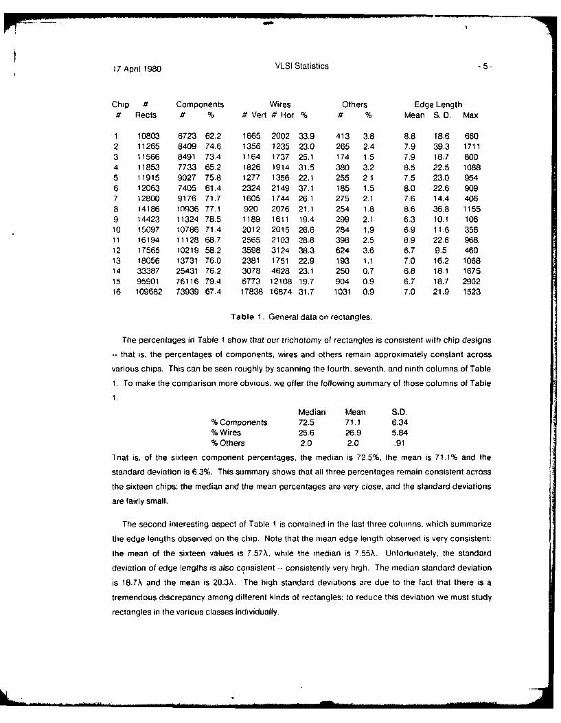
Table 1 contains the first set of data we gathered; we will explain the various columns of the table
by describing in detail its first row. That row describes chip number 1, which contains 10803
rectangles. Of those rectangles, 6723 (or 62.2%) are classified as components. Additionally, 1665
rectangles are vertical wires and 2002 are horizontal wires: therefore a total of 33.9% of all rectangles
are wires (either vertical or horizontal). The remaining 413 rectangles were classified as "others", for
a total of 3.8% of all rectangles. The last three columns of the table report data on all 21606 edges of
the rectanyies (note the number of edges on a chip is twice the number of rectangles). The mean
edge length is 8.8X. with a standard deviation of 18.6. and the longest edge on the chip is 660X.
4Likewise. what is viewed as a wife by the designer may he classilied by thi. lichotomy as many components. This is
because loniq data pilis may be buil tip ot l r lny pieces in hierarchical designs ( or exan ll)l. if a mer rily array is
Constitoil b)y 1 S4quinCetof 'tiStaolnitationrs it 1 ofa synbi defining a singlel( menory cell. then oaclr cl would contain a piece of
the daflta: lie rilirlunoig Ihilitlih the ,ntire niy The mea]suremrents infel diScussion ire based no the rct3nlgles that result
from lirt fully iistanhaleid symbol stirmcrure No Ploil was mare to coalesce separate pieces of the saime wire Although an
analysis of tie 'coalesced" nlictrte is also iirle-,esilg. we present our resilts because inany piogia s that work with chip
designs ale given input in this lotm.
17 April 1980 VLSI Statistics -5-
Chip Ar Components Wires Others Edge Length# Rects # % #Vert #Hor % # % Mean S. D. Max
1 10803 6723 62.2 1665 2002 33.9 413 3.8 8.8 18.6 6602 11265 8409 74.6 1356 1235 23.0 265 2.4 7.9 39.3 17113 11566 8491 73.4 1164 1737 25.1 174 1.5 7.9 18.7 8004 11853 7733 65.2 1826 1914 31.5 380 3.2 8.5 22.5 10885 11915 9027 75.8 1277 1356 22.1 255 21 7.5 23.0 9546 12063 7405 61.4 2324 2149 37.1 185 1.5 8.0 22.6 9097 12800 9176 71.7 1605 1744 26.1 275 2.1 7.6 14.4 4068 14186 109c36 77.1 920 2076 21.1 254 1.8 8.6 36.8 11559 14423 11324 78.5 1189 1611 19.4 299 2.1 6.3 10.1 10610 15097 10786 71.4 2012 2015 26.6 284 1.9 6.9 11.6 35611 16194 11128 68.7 2565 2103 28.8 398 2.5 8.9 22.6 968.12 17565 10219 582 3598 3124 38.3 624 3.6 6.7 9.5 46013 18056 13731 76.0 2381 1751 22.9 193 1.1 7.0 16.2 106814 33387 25431 76.2 3078 4628 23.1 250 0.7 6.8 18.1 167515 95901 76116 79.4 6773 12108 19.7 904 0.9 6.7 18.7 290216 109682 73939 67.4 17838 16874 31.7 1031 0.9 7.0 21.9 1523
Table 1. General data on rectangles.
The percentages in Table 1 show that our trichotomy of rectangles is consistent with chip designs
-- that is, the percentages of components, wires and others remain approximately constant across
various chips. This can be seen roughly by scanning the fourth, seventh, and ninth columns of Table
1. To make the comparison more obvious, we offer the following summary of those columns of Table
1.
Median Mean S.D." Components 72.5 71.1 6.34" Wires 25.6 26.9 5.84" Others 2.0 2.0 .91
1 at is, of the sixteen component percentages, the median is 72.5%. the mean is 71.1% and the
standard deviation is 6.3%. This summary shows that all three percentages remain consistent across
the sixteen chips: the median and the mean percentages are very close, and the standard deviations
are fairly small.
The second interesting aspect of Table 1 is contained in the last three columns, which summarize
the edge lengths observed on the chip. Note that the mnean edge length observed is very consistent:
the mean of the sixteen values is 7.57X, while the median is 7.55A. Unfortunately, thle standard
deviation of edge lengths is also consistent -- consistently very high. The median standard deviation
is 18.7X and the mean is 20.3X. The high standard deviations are due to the fact that there is a
tremendous discrepancy among different kinds of rectangles: to reduce this deviation we must study
rectangles in the various classes individually.

17 April 1980 VLSI Statistics
2.2.2 Data on Components
The data in Table 2 describes the rectangles that were classified as components (that is, those
rectangles with neither edge greater than 10A). The first four columns repeat information fromn Table
1; the fifth column reports the mean edge length of all components on the chip (in X), and the sixthreports the standard deviation of the edge lengths. The edge lengths are remarkably consistent: the
median of the sixteen averages is 3.9A, and their mean is also 3.9X (with a standard deviation of only
.16X). Note that the standard deviations are all very close to 2X.
Chip # Components Edge Length# Rects # %Mean S. D.
1 10803 6723 62.2 3.9 2.02 11265 8409 74.6 3.8 1.93 11566 8491 73.4 4.2 2.34 11853 7733 65.2 4.0 2.15 11915 9027 75.8 3.6 1.96 12063 7405 61.4 3.9 2.07 12800 9176 71.7 3.9 2.08 14186 10936 77.1 3.9 1.99 14423 11324 78.5 3.8 1.610 15097 10786 71.4 3.9 2.011 16194 11128 68.7 4.0 2.012 17565 10219 58.2 3.5 1.613 18056 13731 76.0 3.9 1.814 33387 25431 76.2 3.7 2.015 95901 76116 79.4 4.0 2.116 109682 73939 67.4 3.8 1.7
Table 2. Data on components.
The above data is only a brief sketch of the distribution of components. More detailed studies are
contained in Appendix II: we give two-dimensional histograms of component sizes for the six largest
chips we studied. Those histograms show that the overwhelming majority of components on a chip
are 2A-by-2k~ 2A-by-4, 4A-by-4. or 4?\-by-6X in size, which correspond to minimum-size contact
cuts. polysilicon. diffusion. or metal flashes, and the contact cuts used in "butting contacts" (see
Mead and Conway [ 19801).
2.2.3 Data on Wires
Data on the rectangles that were classified as wires is contained in Table 3. The first five columns
of that table are duplicated from Table 1. The next two columns describe the lengths of the short
edges of the wires (which are, by definition, not greater than 6X). The final three columns describe
the lengths of the long edge of the wires (which are greater than 10OX).

17 April 1980 VLSI Statistics .7-
Chip #Wires Short Edge Long Edge# Rects #Vert # Hor % Mean S. D. Mean S. D. Max
1 10803 1665 2002 33.9 3.1 1.3 25.6 28.3 4612 11265 1356 1235 23.0 2.9 1.3 33.8 106.8 17113 11566 1164 1737 25.1 3.3 1.6 28.3 28.8 3404 11853 1826 1914 31.5 3.1 1.1 24.8 34.6 4885 11915 1277 1356 22.1 2.9 1.2 30.9 41.1 6126 12063 2324 2149 37.1 3.2 1.0 23.4 39.7 6307 12800 1605 1744 26.1 2.9 1.1 27.9 25.8 4068 14186 920 2076 21.1 3.1 1.5 39.4 92.0 8319 14423 1189 1611 19.4 3.2 1.5 23.5 17.0 96
10 15097 2012 2015 26.6 3.2 1.3 22.6 21.2 35611 16194 2565 2103 28.8 3.0 1.2 32.1 40.5 79112 17565 3598 3124 38.3 3.2 1.1 17.0 10.4 32213 18056 2381 1751 22.9 3.2 1.4 26.8 23.5 30314 33387 3078 4628 23.1 3.2 1.5 28.9 40.5 128415 95901 6773 12108 19.7 3.1 1.3 28.3 40.2 177116 109682 17838 16874 31.7 2.9 1.1 22.2 45.6 1523
Table 3. Data on wires.
A number of facts are apparent from Table 3. The first is that most designs have a number of
horizontal wires approximately equal to the number of vertical wires, as one would expect. There are
several designs. however, that are obviously not "balanced" in this sense: chips 3, 8, 14 and 15 all
have at least 50% more horizontal wires than vertical.
The data concerning the short (not greater than 6X) side of the wires is quite consistent. The mean
of the sixteen mean values is 3.1, (with standard deviation .13X) and the median is 3.1X. The
standard deviation of the short edge length is consistently very close to 1 .3A.
The lengths of the longer edge of the wires are more difficult to describe. The median value of the
sixteen mean edge lengths is 27.4k~ and their mean is 27.2X (with standard deviation of 5.1X\). The
typical standard deviation is approximately 40X. Histograms of the distribution of the long edges can
be found in Appendix Ill.
2.2.4 Data on Other Rectangles
Table 4 presents data on the "other" rectangles that were classified as neither components nor
wires. The first four columns are duplicated from Table 1, and the last three columns diescribe the
edge lengths of the components in X.
The median of the sixteen average lengths is 45k their mean and standard deviation are 43. 1A and
8.5A. respectively. The standard deviations are centered around 80X, but vary widely. Two-

17 April 1980 VLSI Statistics -8-
Chip #Others Edge Length# Rects # % Mean S. D. Max
1 10803 413 3.8 39.0 52.3 6602 11265 265 2.4 35.7 71.8 11183 11566 174 1.5 53.7 98.6 8004 11853 380 3.2 45.9 80.9 10885 11915 255 2.1 48.5 103.1 9546 12063 185 1.5 45.7 95.0 9097 12800 275 2.1 36.5 38.1 3538 14186 254 1.8 57.6 128.2 11559 14423 299 2.1 37.2 29.2 10610 15097 284 1.9 33.9 28.6 10611 16194 398 2.5 44.3 75.8 96812 17565 624 3.6 24.4 28.0 46013 18056 193 1.1 56.1 104.9 106814 33387 250 0.7 46.1 88.5 167515 95901 904 0.9 38.2 114.5 290216 109682 1031 0.9 46.6 95.1 1416
Table 4. Data on "other" rectangles.
dimensional histograms showing the distributions of other components are available in Appendix IV.
2.3 Data on PlacementThe data we have mentioned so far has discussed only the shape of the components; in this
section we will describe how those shapes are distributed. There are two questions that we must
answer in this study: in what sort of region are the rectangles placed, and how are they distributed
over that region?
The first issue to be addressed is the region over which the rectangles are distributed. All the chips
that we studied were designed to be enclosed within a bounding rectangle, referred to as its
"bounding box". Table 5 contains data on the bounding boxes of the chips we studied. The first two
columns are duplicated from Table 1. The next two columns give the width and the height of the
chips' bounding boxes in A. The fifth column of the table contains the aspect ratios of each chip.
which is the ratio of the chip's longer dimension to its shorter dimension. The mean aspect ratio is
1.65, while the median is 1.31: the mean is larger than the median primarily because of the one
1.outlying" design with the aspect ratio of 4.57. This data allows us to conclude that most designs are
approximately square.
Having investigated the aspect ratio of the bounding box, we must now study its size (as a function
of the number of rectangles on the chip). To do this, the last column of Table 5 shows the ratio of the
area of the bounding box (measured in ?~)to the number of the rectangles on the chip. Note that this

17 April 1980 VLSI Statistics -9-
Chip #Chip Bounding Box Area (in \ 2)1# Rects D X D Y Ratio # Rects
1 10803 848 1073 1.27 64.232 11265 2072 453 4.57 83.323 11566 840 800 1.05 58.104 11853 896 1088 1.21 82.245 11915 954 856 1.11 68.546 12063 856 910 1.06 64.547 12800 1155 630 1.83 56.858 14186 900 1258 1.43 79.809 14423 1272 657 1.94 57.94
10 15097 850 1110 1.31 62.5011 16194 1190 1106 1.08 81.2012 17565 605 1272 2.10 43.8113 18056 1268 800 1.58 56.1814 33387 1920 963 1.99 55.3815 95901 2944 1676 1.76 51.4516 109682 3019 2370 1.27 65.23
Table 5. Data on chip bounding box.
is the average amount of silicon "real estate" devoted to each rectangle, and not the area of each
rectangle; the inverse of this figure gives the density of rectangles (in average number of rectangles
per A2 area). This ratio remains remarkably consistent across all chips-. the median ratio is 63.5, while
the mean is 65.7 (with standard deviation 12.4).
The above discussion shows that the "typical" bounding box containing N rectangles is a square
of approximately BN1/ 2 \ on each side. The next subject to investigate is the placement of rectangles
over the bounding box: are they spread uniformly over the area, or are they all clustered in a few
dense parts of the chip? Histograms in Appendix V show that the rectangles are indeed spread
uniformly over (most of) the bounding box.
2.4 A Probabilistic ModelThe previous sections in this chapter have focussed on a statistical study of existing VLSI chips.
For use in analyzing potential algorithms for VLSI tasks. we must condense that data into the more
useful form of a probabilistic model. In this section we will study two such models (o1 many possible):
one rather simple arid the other somewhat complicated. Before discussing the particular models,
though. we must address three topics in a more general context: the shape of the bounding box
containing the chips. the placement of the rectangles within the bounding box, and the shape of the
individual rectangles.
The first issue that a modet of rectangles on chips must face is the I)ounding box in which the

17 April 1980 VLSI Statistics -10-
rectangles are distributed. The aspect ratios of Section 2.3 show that the bounding boxes are
approximately square.5 The ratio of chic) area to the number of rectangles shows that the bounding
box should have approximately 64A 2 area for each rectangle in the set.
The second issue a model must face is the distribution of rectangles over the bounding box. The
data of Appendix V shows that the rectangles are indeed uiformly distributed over (most of) the
chip's bounding box. This assumption can also be justified by a priori arguments based on VLSI
design philosophy. One of the aims of a good VLSI design is to make effective use o the silicon area.
This implies that the design will fill its bounding box rather uniformly. Although there are typically
sparse regions near the edges of the design (containing long wires, bonding pads and pad drivers),
the central part of the chip has a much higher (and almost uniform) density of small rectangles that
perform most of the computation and data manipulation. The fixed number of layers available for a
design (in nMOS there are typically six) and the design practice of not overlapping many rectangles
on one layer combine to limit the number of rectangles that cover any given point on the chip; this
together with the lower bound on rectangle size implies a constant upper bound on the density of
rectangles. Economic arguments provide a lower bound: there is no reason to leave large blank
spaces in a design.
The third issue to be faced is the shape of the individual rectangles. Fortunately, we have a great
deal of data on rectangle shapes in Section 2.2 and Appendices II through IV.
We can now combine these facts regarding the size and shape of the bounding box, the placement
of rectangles, and the shape of rectangles into a probabilistic model. The simplest possible model of
an N-rectangle design is that the N rectangles are squares with edge length 7.6, uniformly
distributed on [0, 8N' 1 2,] 2 . (The value 7.6A is from Table 1, and the 8X is from Table 5.)
On the other hand, we could postulate a much more complex model for generating a set of N
rectangles. We first choose an aspect ratio R uniformly from [1,21, and a sparsity S uniformly from
[44,84]. (S is the total amount of silicon real estate per rectangle in the bounding box.) We then set
the short side of the bounding box to be (NS/R)1 2 \, and the long side to be (RNS) t1 2X. We then
distribute the following rectangles uniformly over the bounding box:
* (.72)N components, each with side lengths chosen uniformly on [2A.10X ] 2 (A moresophisticated method could sample a stored 10-by-10 table giving the probability ofrealizing each pair of lengths: such a table could be generated from the data in Appendix
A number of engineemiig and Pconomic ren-sons dictate that the chip's bounding box should be close to squnie. This oftenmakes wire.bonding easier. maid usually makes mo, e eificient use of the package cavity The authors reqtel to have to point outthat in the designs we siudied. there was motivation for "long and skinny" chips. rumor s t tie design community iepoi ted thatsuch desiqns were note likely to ie placed on inulliliolect chipsl Most of their chills with extremely high aspect Iatios werevery small and ithreitore filtered by ou, criterion of examining only chips with at least 10,0W(X rectangles.
II,
17April980 VLSI Statistics -11-
II
II.)
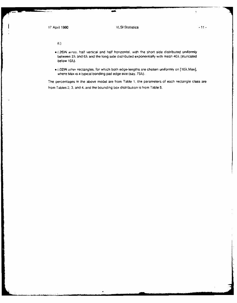
( 26)N wires, half vertical and half horizontal, with the short side distributed uniformlybetween 2A and 6X and the long side distributed exponentially with mean 40'k (truncatedbelow 10A).
* (.02)N other rectangles. for which both edge-lengths are chosen uniformly on [lOA.MaxJ,where Max is a typical bonding pad edge size (say, 75A).
The percentages in the above model are from Table 1, the parameters of each rectangle class are
from Tables 2. 3, and 4, and the bounding box distribution is from Table 5.
17 April 1980 VLSI Statistics -12-
3. Applications of the StatisticsIn this chapter we will consider a set of geometric subproblems that arise in layout, routing and
design rule checking called the geometric intersection problems. In the abstract problem we are
given a set of objects in the plane and must report all pairwise intersections among the objects. In
concrete applications the geometric objects are usually components on a chip, and the intersections
are potential "trouble areas", such as design rule violations or a place for a crossover.
Much previous work has been done on geometric intersection problems. Baird [1978], Lauther
[1978, McCaw [1979], and Wilcox. Rombeek and Caughey [1978] all describe programs for
computing geometric intersections that have actually been used in the design of masks. Although all
of their programs are much faster than naive geometric intersection programs, they are still slower
than desired and lack a solid theoretical basis. Theoretically sound algorithms have been given by
Shamos [1978], Bentley and Ottmann [1979] and Bentley and Wood [1980], but they are very complex
to code and fail to exploit many of the situations that arise in practice.
In this chapter we will study a particular geometric intersection problem that calls for intersecting
rectangles. In Section 3.1 we develop a theoretical algorithm that performs very well for input
rectangles drawn from the distributions studied in Chapter 2. Section 3.2 then shows how the
theoretical algorithm can be efficiently implemented on the secondary storage media necessitated by
the large size of current VLSI designs. We discuss the algorithm's potential for VLSI applications in
Section 3.3.
3.1 An Algorithm for Finding Rectangle IntersectionsIn this section we will examine an algorithm for solving the following problem.
The Rectangle Intersection Problem -- Given a set of N rectangles in the plane, each ofwhich has sides parallel to the coordinate axes, report each intersecting pair of rectangles(by calling some procedure).
The operation of intersecting rectangles is fundamental in many VLSI tasks: we will return to these in
Section 3.3. A straightforward way of solving the Rectangle Intersection Problem is to compare all (N)
pairs of rectangles. This method is very easy to code and efficient for small values of N, but the O(N2)
running time is prohibitive for large designs. Bentley and Wood [1980] describe an algorithm for
solving the problem in O(N Ig N + k) worst-case time, where k is the number of intersecting pairs
found. Their algorithm. however, is primarily a theoretical device, being difficult to code and having a
large constant factor "hidden" in the 0-notation. In this section we will investigate an algorithm that
exploits the probabilistic models of Section 2.4 to yield an algorithm with expected running time
proportional to N.

17 April 1980 VLSI Statistics -13-
The algorithm we will study in this section exploits the probabilistic models of the last chapter to
solve the rectangle intersection problem in fast expected time. Before studying that algorithm, it is
important for us to summarize the salient points of the probabilistic models from an algorithmic
viewpoint. The first important fact is the uniformity of the distribution of the rectangles: this
uniformity facilitates the use of bins to store data. (Bins work very poorly for highly-clustered data, but
have excellent performance for uniform distributions). Equally important is the small average edge
length of a rectangle (7.6X) compared to the average chip width (8N1 /2X). We will find these
measurements very helpful as we calculate the optimal size of a bin.
The algorithm for reporting all intersections among a set of rectangles is based on a bottom-to-top
scan of the set of rectangles. At each time during the scan, all rectangles currently intersecting the
horizontal scan line are represented as a set of one-dimensional line segments. When the bottom of a
new rectangle is encountered, the rectangles it intersects are found by checking which line segments
its segment intersects; its segment is then added to the set. When the top of a rectangle is found, its
segment is deleted. In this way, only the rectangles currently intersecting the scan line need be kept
"active" at one time, yet all intersecting pairs are correctly reported.
We can now describe the algorithm more precisely. The input is a set of rectangles, each of which
is described by a unique name, four real numbers (giving the extreme left, right, bottom and top
coordinates), and any other information needed for the VLSI application. The "output" is a call to
procedure REPORT for every intersecting pair of rectangles. We will make use of two primary data
structures. The EL (for "Event List") sequence contains two entries for each rectangle one for its
bottom edge and one for its top. This list is sorted by y-coordinate, in increasing order. The other
data structure is the set of line segments, called SS for "Segment Set", that intersect the hypothetical
scan line (we will discuss the implementation of SS later). With this background, the algorithm is
described as follows.
Algorithm A
1. [Build the event list.]a. For each rectangle in the input set, create two records in the event list EL: one
corresponding to the bottom, one to the top.b. Sort EL by increasing y-value. If various rectangles have equal y-values. then place
the bottom edges before the top edges.
2. [Scan through the event list.]a. Initialize SS to represent the empty set.b. Scan through EL in increasing order by y-value. As each record R in EL is visited,
take one of the following actions.i. If R represents the bottom of a rectangle, then first check the line segment
corresponding to R (that is. the proiection of the rectangle onto the x-axis) forintersection with any other segments in SS (reporting a., intersecting pairs),and then insert that segment into SS.

17 April 1980 VLSI Statistics - 14-
ii. If R represents the top of a rectangle, then delete its segment from SS.
The correctness of Algorithm A is based on the fact that if any two rectangles intersect, then they
must be "act~ve" (that is, present in SS) at the same time and will therefore be reported in Step 2.b.i.
We will now briefly analyze the time required by Algorithm A. Step 1.a requires O(N) time, and
straightforward implementations of the sort in Step 1.b require O(N Ig N) time. We note that the time
requirad to sort can be reduced to O(N) expected time by using the bin method described by Weide
[1978]; we will return to the running time of this step in the next section. The initialization cost of Step
2.a is dependent on the implementation of SS, as are the costs of the N insertions and deletions both
into and from SS in Steps 2.b.i and 2.b.ii. Our task now is to find an implementation of SS to facilitate
rapid insertion and deletion of line segments.
We will implement the SS structure by dividing the portion of the x-axis on which the rectangles fall
into a set of bins. For instance, if all x-values of rectangles lie between OA and 800A, then we could
have one hundred bins, each of width 8X. The set of bins is implemented in a program as an array of
pointers; each pointer points to a linked list of segment names that currently overlap that bin. This
situation is illustrated in Figure 1. To insert a new segment into this structure, we merely insert its
name into all bins overlapping the segment; to delete it, we traverse the same set of bins and delete
the segment name from the linked list of each. To check what segments in SS a new segment X
overlaps, we visit each bin in which X fails and compare X against all elements in the bin; careful
bookkeeping allows us to be sure that no pair of segments is reported twice.
bbbc cIa Ia Ia Ia Ib I b Ic I I I I Id Id Ia- 5---
C
Figure 1. Segments represented in bins.
The final task we face in the implementation of SS is the specification of exactly how many bins
there should be. or alternatively, the width of each bin (for given one, we can determine the other). It
is at this point that we make crucial use of the data in Section 2.4: we choose the bin width to be
(approximately) the average width of a rectangle, so that each segment is placed in two bins, on the
average. By the models in Section 2.4. this imolies that each bin has width of approximately 8X, and
the total number of bins is the square root of the number of rectangles. In this implementation, the
initialization of the bins requires O(N 11 2 ) time: we will shortly show that insertion and deletion have
only constant cost on the average. The expected total running lime of Stage 2 is therefore O(N).
There is one fact that has yet to be established to prove the above claim of linear running time for
Stage 2 of algorithm A. We require that the expected number of rectangles in a bin be a constant

17 April 1980 VLSI Statistics15
(independent of N), which implies that insertion and deletion have constant cost on the average. The
empirical observations of the program's running time to be presented in the next section supports this
claim. We can also show that the claim holds under the models of rectangle distribution and size
discussed in Section 2.4. Consider first the simple model of an N-rectangle design: the N rectangles
are squares with edge length 7.6k, uniformly distributed on [0, 8N112X\] 2: we must determine the
expected number of rectangles in SS at any time. The probability that a given square intersects a
given scan line is (7.6X)/(8N"/ 2X). (Because the square intersects the scan fine defined by y = S if the
y value of the lower edge of the square falls within the range [S-7.6X. 5]). The expected number of
squares intersecting the scan line at any given time is simply the total number of squares multiplied by
the proo~ability that an individual one intersects the scan line, which is (7.6XN"-)/(8X). or .95N 1 .I
Each of the N1 12 bins representing the SS has a width of 8X; hence each square is entered into two
(or possibly just one) bins. Since the squares are uniformly distributed, the bins are evenly filled and
each bin contains approximately two squares; this establishes the claim. Now consider the more
complicated model for generating the N rectangles which is based on the trichotomy of components,
wires and others. The constant expected number of entries in each bin can be proved in a manner
similar to the proof for the simple model above. Of critical importance is that (1) other rectangles have
an upper bound on their edge length, and that (2) wires have a constant average length (although the
observed distribution does not impose an a priori upper bound on the length of a wire.)
In preparation for the next section we present a quick summary of algorithm A, with a view toward
implementation. The first stage consists primarily of a sort, and the second stage is a linear scan
through the sorted output of Stage 1. This scan has the pleasant property that it can i.erform all
necessary processing to report intersections using only 0(N112) storage. Note that the only
communication necessary between the two stages of the algorithm is a sequential file giving the
sorted event list.
3.2 A Pascal ProgramIn this section we will describe a set of three computer programs that together implement Algorithm
A of the last section. Before going into the details of the individual programs. we will first give a brief
overview of the system as a whole. The input to the system is a disk file containing the rectangles to
be checked for pairwise intersection, and the "output" is a set of calls to a REPORT procedure (which
performs some desired operation) reporting each intersecting pair of rectangles exactly once.
Algorithm A is divided into two primary stages: Stage 1 creates a sorted "Event List" named EL, and
Stage 2 scans through EL. The EL structure is implemented in this system as a (sorted) disk file. With
this overview in mind, we can now describe the computer implementations of the two stages of the
algorithm.
17 April 1980 VLSI Statistics -16-
The purpose of Stage 1 is to create the EL file and then sort it. In the first substep (Step 1-a), a
simple (40 line) Pascal program creates an unsorted version of the EL file by representing each
rectangle in the input file twice: once for the bottom edge and once for the top. The records of this
file are then sorted into increasing order by y-coordinate, with a secondary sort key chosen so that
events representing bottom edges precede top edges for equal y-values. The sorting program to
accomplish this in our system is a standard system sorting program. As mentioned in Section 3.1, we
could use a linear expected-time sort based on bins (see Weide [19781) but this would have been
much more difficult to code. On the other hand, it is possible to avoid an explicit sort altogether by
generating the rectangles in sorted order from the CIF hierarchical description: at any time, the
symbol with the lowest bounding box is expanded first.
The second stage of Algorithm A scans through the sorted event list, performing operations on the
segment structure SS. The Pascal program implementing this scan contains about 400 lines of code,
of which only 220 are for the algorithm itself, while the remaining 180 are for testing and timing. The
number of bins in SS was chosen to be equal to the square root of the number of rectangles, that is,
N112. By the data of Chapter 2, this implies an average bin width of approximately 8A.
Extensive measurements of the time and space usage of the program were performed. The
program corresponding to Step 1.a of the algorithm was I/O bound. Step 1 .b was a standard system
sort, which has been studied in great detail elsewhere (see, for example. Knuth [1973, Section 5.41).
We therefore concentrated our measurements on the time and space requirements of Stage 2 of the
program.
The performance of the program implementing Stage 2 is summarized in Table 6. The Pascal
programs were run on a DEC PDP-KL10 (ARPANET Host CMU-10A). The programs were executed on
VLSI designs from recent Xerox PARC multiproject chips that contain between 4.000 and 12,000
rectangles.6 The first row of the table describes the performance of the program on a chip containing
4689 rectangles. There were 219 elements in the segment set SS on the average, and SS was never
larger than 475. The ratio of the maximum size of SS to the root of the number of rectangles is 6.94.
The running time of the program was 8.9 seconds, and the amortized time per rectangle is 1.9
milliseconds. The number of rectangle intersections found was 14441, and the ratio of the chip's
width to its height was 3.1.
As predicted, the running time of the program implementing Stage 2 of our algorithm is
proportional to N: the time per rectangle is between 1.73 and 1.93 milliseconds. The rectangle sets
used for these measurements include features from all layers of a chip design. Hence an average
6For hisiorical reasons (the transfer of VLSI computing at CM13 from a PDP 10 to a VAX 11 780). we report the running time
of our progrms oin a set of estlher (and smatler) miltlipioiect chip designs.

17 April 1980 VLSI Statistics -17-
# Rects Segment Set Size Time Time/N # Ints Aspect Ratio= N) Mean Max Max/N /2 (sec) (msec) (Hor/Vert)
4689 219 475 6.94 8.9 1.9 14441 3.14960 86 172 2.44 8.6 1.73 11783 1.35272 11 246 3.39 9.3 1.76 14441 1.57176 150 359 4.24 12.9 1.89 18949 1.37416 123 254 2.95 14.3 1.93 22166 .7311316 55.8 124 1.17 20.7 1.83 30565 .22
Table 6. Measurements for Stage 2 of Algorithm A.
rectangle intersects a relatively large number of other rectangles: in our case this number lies
between 3.5 and 6. Many applications need intersections of rectangles only from a subset of the chip
layers. and the algorithm will perform even better in that case: the number of intersections per
rectangle will be lower, and the SS can be searched more rapidly.
The total number of memory words used in Stage 2 is proportional to the number of bins plus the
maximum number of rectangles ever in SS at one time. The fourth column of Table 6 shows that this
is bounded above by approximately 4RN1 / 2 in practice, where R is the aspect ratio of the chip. (The
simple probabilistic model of Section 2.4 predicts RN1/ 2 : the observed increase is due to the local
clustering in real designs not accounted for in our model.) This has a very pleasant implication for the
main memory utilization of the algorithm: note that if N is one million and the aspect ratio is unity, then
at most four thousand rectangles are ever present in main memory at the same time
Our program was designed to scan the chip from its bottom to its top, and this led to severe space
inefficiency for chips that were "short and fat". Because the rectangles are distributed uniformly over
the chip, the number of rectangles intersecting the scan line will be proportional to the line's length,
which is less if the chip is scanned in the "tall and skinny direction". (Note that the length of the scan
line is less by a factor of the square of the aspect ratio.) Recall that the space used by the algorithm is
directly proportional to the number of rectangles intersecting the scan line. This analysis, together
with the data of Table 6, suggests strongly that design rule checkers should be designed to "rotate"
their inputs, so the chips are always scanned in the beneficial direction.
3.3 Applications in VLSI TasksVLSI technology will soon allow several hundred thousand devices in a single IC design. The
lowest common denominator for these designs is the geometric specification of the shapes on the
mask layers. Design rule checking is the process of determining whether certain interrelationships
are maintained between those shapes: for example, whether all unrelated polysilicon and diffusion
lines are separated by at least 1 X. Design rule checking programs are the "syntax checkers" of the IC

17 April 1980 VLSI Statistics - 18-
world -- they guarantee that the form of the chip is correct (but not, of course, that it does what the
designer intended).
Algorithm A of Section 3.1 can be used in design rule checking. Most minimum width, minimum
clearance, and enclosure checks can be performed by the combination of programs to expand/shrink
rectangles, perform logical operations (for example, forming the logical OR of two layers to produce a
third), and an intersection reporter. Such systems are essentially batch oriented: an entire design file
is checked at once and all design rule violations reported. The fast rectangle intersector is the
workhorse here, processing a large number of rectangles in a single pass, Note that the time required
by the rectangle intersector is linear in the number of rectangles, and its space requirements are
proportional to the square root of the number of rectangles.7
While batch-oriented geometric design rule checkers are in wide use, interactive systems can
provide valuable feedback as designs are entered. In an operator-guided placement and routing
system, violations can be automatically flagged as each cell is placed. It may also be possible to hide
a considerable amount of computation in the operator's "think" time. Straightforward extensions of
the algorithm above make such incremental checks easy. The chip can be divided into two-
dimensional bins, where a rectangle is put into all the bins it overlaps. Once these bins have been
constructed. it is simple to find which existing rectangles intersect a given new rectangle. The data of
Chapter 2 and Appendix V ensures that this approach will be very fast: the shape data tells us that
rectangles are small (and will therefore fall into few bins), and the uniformity of the placement data
tells us that only relatively few rectangles will fall into any particular bin.
7As appealing as a last geomelric design rule checker may be. we believe that faster design rule checkers will lakeadvantage of the high level information in hieraichical IC designs Such lesigns consist of cells that implement a particularfuiction. connected together t y some amount of wiing Each cell in turn consists of an agglomeration of cells, components.and wioes, the lowest level cells ate meePly collections tf components and Wires Peilotnimitce m1piovemlents imay be achievedbv taking advtiage of the stiuctufi, in ilie desiqn. For instance. if is necessay to chck any pailiciila! cell only once --st bsequent placements of tie cell nted be checked only if they ovti lap, of et shapes 13v intrsecting thie boinditig box of acell befoi e "ex loding 'the cell into its coonstituelt par is. a quick yes/ no del, erriinatum cjrin be made! of whelhei anything wilhinthe cell might intersect previously placed cells. A single intersection check can thereltne eliminate many rectangles flomconsideration The fast intersection algorithmn might be useful for such geometric manipulations.
17 April 1980 VLSI Statistics . 19-
4. ConclusionsThere are two main contributions in the work of the previous chapters. The first contribution is the
program for finding geometric intersections: it is easily coded, very fast, and space-efficient.
Preliminary comparisons indicate that it is much faster than previous programs for similar tasks. The
second, and more fundamental. contribution of this work is the data on the distribution of chip
components and the methodology for using such data to design fast programs. We feel that the
techniques we have used here will prove to be of broad applicability in constructing design aids for
VLSI systems.
A great deal of further work remains to be done. The algorithm of Chapter 3 is being used in a
design rule checker currently under development at Carnegie-Mellon. An important open problem is
to gather more data on VLSI designs: two particularly interesting questions are whether the
conclusions we drew from this data will "scale up" to designs an order-of -magnitude larger, and how
our data will compare with industrial chips (as opposed to the Mead-Conway style designs). An
interesting problem in VLSI design is to employ more knowledge than the strictly geometric issues
that we have studied here-, it is therefore important to study the hierarchical structure inherent in the
CIF representation of a VLSI design.
Acknowledgements
We are grateful to the chip designers mentioned in Appendix I for allowing their designs to be used
in this study. and to Bill Eddy and Bob Sproull for their helpful comments.

17 April 1980 VLSI Statistics -20-
References
Baird, H. S. [1978]. "Fast algorithms for LSI artwork analysis," Journal of Design Automation andFault-Tolerant Computing 2, 2, pp. 179-209.
Bechtolsheim, A. and T, Gross [1980], "A Parallel Search Table for Logarithric Arithmetic," paperpresented at the M.I.T. Conference on Advanced Research in Integrated Circuits, January,1980.
Bentley, J.L. and T. Ottmann [1979]. "Algorithms for reporting and counting geometricintersections," IEEE Transactions on Computers C-28, 9, pp. 643-647, September 1979.
Bentley, J. L. and D. Wood [1980]. "An optimal worst-case algorithm for reporting intersections ofrectangles," to appear in IEEE Transactions on Computers.
Conway, L., A. Bell, M. Newell, R. Lyon, and R. Pasco [1980]. Implementation Documentation for theMPC79 Multi-University Multiproject Chip-Set, Xerox PARC Report, January 1980.
Clark, J.H. [1980], "A VLSI Geometry Engine for Computer Graphics," paper presented at the M.I.T.Conference on Advanced Research in Integrated Circuits, January, 1980.
Conway, L., A. Bell, M. Newell, R. Lyon, and R. Pasco [1980], "Implementation Documentation for theMPC79 Multi-University Multiproject Chip-Set," Xerox PARC Report, January, 1980.
Holloway, J., G. Steele, G.J. Sussman, and A. Bell [19801, "The SCHEME-79 Chip," paper presentedat the M.I.T. Conference on Advanced Research in Integrated Circuits, January, 1980.
Hon, R. W. and C. H. Sequin [1980]. A Guide to LSI Implementation, 2nd edition, Xerox PARC TR SSL79-7, Chapter 7, January 1980.
Lauther. U. [1978]. "4-dimensional binary search trees as a means to speed up associative searchesin design rule verification of integrated circuits," Journal of Design Automation and Fault.Tolerant Computing 2, 3, pp. 241-247.
McCaw. C. R. [1979]. "Unified shapes checker -- a checking tool for LSI," Proceedings of theSixteenth Design Automation Conference, pp. 81-87, June 1979, ACM.
Mead, C. A. and L. Conway [1980]. Introduction to VLSI Systems, Addison-Wesley, Reading, MA.,1980.
Shamos, M. I. [19781. "Problems in' computational geometry," unpublished Ph.D. Thesis, YaleUniversity, 1978.
Weide. B. W. 119781. "Statistical methods in algorithm design and analysis", Ph.D. Thesis. Carnegie-Mellon University, August 1978.
Wilcox. P.. H. Rombeek, and D. M. Caughey [19781. "Design rule verification based on onedimensional scans". Proceedings of the Fltteenth Design Automation Conference, June 1978.ACM.
17 April 1980 VLSI Statistics -21 -
I. Description of the ChipsMost of the following chips were designed as part of a VLSI course given at Stanford University by
Rob Mathews and John Newkirk. The designs were implemented on a multiproject chip (MPC79)
managed by Xerox PARC, with data communication provided by the ARPANET, masks by Micro Mask,
Inc.. and wafer fabrication by Hewlett-Packard. (For more details see Conway et. al. [1980].) In
several cases, papers are available that describe the design in detail. Four of the projects have not
yet been implemented, as they were not completed by the final MPC79 deadline. Those projects will
probably be implemented on future multiproject chips.
1. Bill Frolik and Roderick Young -- Digital Tinier.
2. Rob Mathews and John Newkirk -- Firecode Chip.
3 Huang -- Not implemented.
4. Forest Baskett -- Ethernet Synchronizer.
5. Marc Hannah and Peter Eichenberger -- Rectangle Generator.
6. Mike Tarsi and Nagatsugu Yamanouchi -- Multifunction Digital Clock.
7. David Noice and Neil Midkiff -- Multiplier/Divider.
8. Sytwu -- Not implemented.
9. Gluss -- Not implemented.
10. Redford -- Not implemented.
11. Jim Clark -- Graphics ALU (see Clark [1980]).
12. Andy Bechtolsheim and Thomas Gross -- Parallel Search Table for Log Arithmetic (seeBechtolsheim and Gross [ 1980]).
13. Matt Herndon and Jeff Thorson -- Typesetting Machine.
14. Synth -- Part of a digital speech synthesizer designed by Jim Cherry of MIT.
15. Filters -- Part of a speech recognition system designed by Dick Lyon at Xerox PARC.
16. SChip2 -- The second version of a Lisp microprocessor designed by Sussman, Steele,and Holloway from MIT and Bell from Xerox PARC (see Holloway. et. al. [1980]).

17 April 1980 VLSI Statistics -22-
1I. Component HistogramsIn this appendix we will present histograms that give more detail on the distribution of components.
The histograms are contained in Figures 1 through 6; they describe chips 11 through 16, respectively.
Figure 1 describes chip 11. The first three lines of that figure summarize data from Table 2 of Section
2.2.2. The next part of the figure gives a two-dimensional histogram of the component distribution.
For instance, there were 1059 2X-by-4X components (that is. 2X wide by 4X high). The five x's in that
box indicate that these 1059 components are approximately half the number of the maximum number
of components in any of the one hundred sizes (that is, the 2125 4X-by-4X components, which have
ten x's). The final thirteen lines in the figure "linearize" this two-dimensional data by summarizing the
longest edge of the components. For instance, 2139 components had a longest edge of exactly 6A\
(or 19.2% of all components), and 81.2% of the components had both edges less than or equal to 6X
in length.
A number of facts are readily apparent from these tables. The first is that there are few
components that have an edge length of lA. Since a 1 X edge violates Mead and Conway's design
rules, all such components were in fact part of logos. The second obvious fact is that most
components were 2X-by-2X, 2X-by-4X, 4X-by-4X, or 4X-by-6X (or rotations of those by 900). Finally,
we note that most component edge lengths were less than or equal to 6N. From the summaries at the
bottom of the figures. we see that on all chips. 78% or more of the components had longest edge less
than or equal to 6X. Of the remaining 22% with one edge greater than 6X, very few had both edges
greater than 6X (observe that the upper right 4A\-by-4i\ rectangle of each histogram is very sparsely
populated). This implies that even if we had changed our definition of component to all rectangles
with both edges less than or equal to 6X, our results would have changed little.

17 April 1980 VLSI Statistics -23-
16194 rectangles11128 components (68.7% of total)Component edge length : Mean 4.0, Standard deviation 2.0
Distribution of component sizes
10 x x x x x x132 1 31 12 1 1
9 x x x x
176 86 16 2
8 x x x x x48 3 116 314 3
S x X X X X133 7 14 4 23
X6 X X XX X X x X X X
299 .2 558 26 311 7 133 28 15
171 2 40 31 16xx x xxxxx x
4 xxx x xxxxx X xx x x x x1059 331 2125 38 625 36 38 77 12
3 x x x x x x x x x
22 40 295 3 1 6 1 2 1
2 xxxx x xx x x x x x x1707 47 790 164 301 146 96 307 64
32
1 5 6 7 8 9 1;
Component size breakdownLongest Count Cumulative
edge1 0 0.0% 0.0%
2 1739 15.6% 15.6%3 109 1.0% 16.6%4 4600 41.3% 57.9%.5 449 4.0% 62.0%6 2139 19.2% 81.2%7 376 3.4% 84.6%8 752 6.8% 91.3%9 694 6.2% 97.6%10 270 2.4% 100.0%
Figure 1. Components of chip 11.

17 April 1980 VLSI Statistics -24-
17565 rectangles10219 components (58.2% of total)Component edge length : Mean 3.5, Standard deviation 1.6
Distribution of component sizes
10 x x44 24
9 x x x1 10 20
8 x x x x5 11 36 20
7 x x x68 66 66
6 x x x x x x x23 1 292 22 2 26 11
5 x x x x86 2 1 4 20
I xx x4 xx x xxxxx x x x x
962 233 3138 12 222 90 10
3 x X X X X X X X6 17 177 11 11 3 4 2
2 xxxx X xx x x x x x x
2583 115 1193 60 134 97 88 44 143
X2
1 2 3 4 5 6 7 10
Component size breakdownLongest Count Cumulativeedge
1 0 0.0% 0.0%
2 286 25.3% 25.3%3 138 1.4% 26.7%4 5703 55.8% 82.5%.5 176 1.7% 84.2%6 727 7.1% 91.3%7 234 2.3% 93.6%8 276 2.7% 96.3%
9 90 .9% 97.2%10 289 2.8% 100.0%
Figure 2. Components of chip 12.

17 April 1980 VLSI Statistics -25-
18056 rectangles13731 components (76.0% of total)Component edge length : Mean 3.9, Standard deviation 1.8
Distribution of component sizes
10 x x x295 4 128
9 x x x44 2 90
x x x74 18 233
71 x x303 1
61 x x x x x x x96 509 2 39 33 46 8
5 x x x90 1 8
xxxxx41 x x x xxxxx x x x x x
28 705 538 4862 580 28 197 4 9
3 x x28 436
x x2 x xx x x x x x x x x
29 1700 96 1083 134 354 129 517 35 159
x56
2 3 4 5 6 7 8 9 10
Component size breakdownLongest Count Cumulativeedge
1 0 0.0% 0.0%2 1729 12.6% 12.6%3 124 9% 13.5%4 7708 56.1% 69.6%5 225 1.6% 71.3%6 1588 11.6% 82.8%7 461 3.4% 86.2%8 1072 7.8% 94.0%9 221 1.6% 95.6%10 603 4.4% 100.0%
Figure 3. Components of chip 13.

17 April 1980 VLSI Statistics -26-
33387 rectangles25431 components (76.2% of total)Component edge length : Mean 3.7, Standard deviation 2.0
Distribution of component sizes
10 x x x x58 47 590 2
9 x x x x x x177 31 51 25 8 1
8 x x x x156 70 43 77
7 x x x65 294 32
6 x x x x x x x50 393 1098 132 1062 1 1
5 x x x x x28 233 2 168 21Ix xx x
4 x x x xxx x x x x x39 884 1187 3825 1 1782 85 4 46
3 x x x x x12 670 17 870 1
xxxxx2 x xxxxx x X x x x x x x
8 7569 347 1097 579 93 146 265 770 204
1 x x x2 11 1
1 2 3 4 5 6 7 8 9 10
Component size breakdownLongest Count Cumulativeedge
1 2 .0% .0%2 7588 29.8% 29..8%3 1046 4.1% 34.0%4 7903 31.1% 65.0%5 1011 4.0% 69.0%6 3549 14.0% 83.0%7 537 2.1% 85.1%8 1779 7.0% 92.1%9 1068 4.2% 96.3%
10 .948 3.7% 100.0%
Figure 4. Components of chip 14.

17 April 1980 VLSI Statistics -27.
95901 rectangles76116 components (79.4% of total)Component edge length : Mean 4.0, Standard deviation 2.1
Distribution of component sizes
10 x x x x x x x1597 2 1506 4 1 29 2
9 x x x x x x433 37 195 56 36 1392
8 x x x x x x1108 31 59 255 29 4
7 x X x x x x x2408 8 78 59 1420 7 1
61 x x x x x x x x2013 29 2811 1 214 9 1449 289 1
x
6fX x x x x869 247 2864 2 36
X X xxxxx Xx x xxxxx x xx x x x x
3357 3365 16059 52 4092 1 260 208 98
3 X X X X X X293 127 2129 58 25 2
Ixxxx.21 AXXAA X A X X X X2 XXX xx x x x x x x x x
14 14947 576 3898 1230 491 493 999 1040 683
x x4 24
1 2 3 4 5 6 7 8 9 10
Compo:ient size breakdownLongest Count Cumulativeedge
1 0 0.0% 0.0%2 14965 19.7% 19.7%3 996 1.3% 21.0%4 28808 37.8% 58.8%.5 5262 6.9% 65.7%6 9711 12.8% 78.5%7 4476 5.9% 84.4%8 4286 5.6% 90.0%9 3686 4.8% 94.8%
10 3926 5.2% 100.0%
Figure 5. Components of chip 15.

17 April 1980 VLSI Statistics -28-
109682 rectangles73939 components (67.4% of total)Component edge Tength : Mean 3.8, Standard deviation 1.7
Distribution of component sizes
10 x x x x x1193 2 183 33 1
9 x x x x937 2 83 64
8 x x x x x9 550 49 189 395
7 x x x x x X369 34 489 49 34 49
6 x x x x x x x x x441 4 3136 135 425 1 365 342 312
SI x x550 414 1
I xxxxx41 x x xxxxx x x x x x
2448 999 31891 128 2004 64 735 174 249
3 x x x x x x x x x1363 8 881 18 48 1 51 78 28xx
2 I x xx x x x x x x x x74 13954 512 2860 333 1126 294 683 1557 522
Sx x14 2
1 2 3 4 5 6 7 8 9 10
Component size breakdownLongest Count Cumulativeedge
1 0 0.0% 0.0%2 14042 19.0% 19.0%3 1883 2.5% 21.5%4 39081 52.9% 74.4%5 1443 2.0% 76.3%6 7320 9.9% 86.2%7 1301 1.8% 88.0%8 3060 4.1% 92.1%9 3237 4.4% 96.5%10 2572 3.5; 100.0%
Figure 6. Coiivpoiieiiis at chip 16.

17 April 1980 VLSI Statistics -29-
Ill. Wire HistogramsThe histograms of this appendix give details on the distributions of the long edges of the rectangles
classified as wires. Figures 7 through 12 give the data for chips 11 through 16. The first five lines of
each figure repeat data from Table 3 of Section 2.2.3. The remaining part of the figure is a histogram
of the distribution of long edges, giving both the absolute number in each range, and the cumulative
percentages of all wires. For example. on the wires of chip 1 I (Figure 7) there were 111 long edges
between 30A and 34N, and 77.9% of all long edges were less than or equal to 34N.
The following table summarizes the distribution of wires on the six chips studied in this appendix.
Chip # <(25A < 50A < 1O0A <(150A < 195A
11 68.1 82.8 96.9 98.5 98.912 95.0 97.7 99.9 99.9 99.913 68.2 95.1 98.5 99.3 99.514 60.0 90.1 97.2 98.9 99.115 69.1 87.2 97.0 99.2 99,516 84.9 96.4 98.2 99.1 99.3
This says that 68.1 % of the wires on chip I1I had a long edge less tha-, 25A. and 98.9% had a long
edge of less than 195X. To summarize the above data, the "typical" chip has 70% of its edges less
than 25A in length, 90% less than 50A, 97% less than 1OGA, and 99% less than 150A.
The above summary shows that the number of wires with long edges decreases very rapidly. As a
first approximation. we might assume that the wire lengths are distributed exponentially; however.
there is too much "activity" in the tails of the distributions for this to be the case. Determination of the
exact character of this distribution remains an open problem.

17 April 1980 VISI Statistics - 30 -
16194 rectang. s4668 wires (28.8% of total)2565 vertical, 2103 horizontal.Wire width Mean 3.0, Standard deviation 1.2Wire length Mean 32.1, Standard deviation 40.5, Max 791
Distribution of wire lengthslength count % of
total
0 - 4 0 0.05 - 9 0 0.010 - 14 1198 25.7 xxxxxxxxxxxxxxxxxxxxxxxxxxxxxxxxxxxxxxxxxxxxxxxxx15 - 19 1149 50.3 xxxxxxxxxxxxxxxxxxxxxxxxxxxxxxxxxxxxxxxxxxxxxxx20 - 24 832 68.1 xxxxxxxxxxxxxxxxxxxxxxxxxxxxxxxxxx25 - 29 345 75.5 xxxxxxxxxxxxxx30 - 34 111 77.9 xxxx35 - 39 87 79.7 xxx40 - 44 106 82.0 xxxx45 - 49 35 82.8 x50 - 54 36 83.5 x55 - 59 64 84.9 xx60 - 64 22 85.4 x65 - 69 46 86.4 x70 - 74 287 92.5 xxxxxxxxxxx75 - 79 85 94.3 xxx80 - 84 16 94.7 x85 - 89 8 94.8 x90 - 94 36 95.6 x95 - 99 40 96.5 x
100 - 104 22 96.9 x10⁵ - 109 41 97.8 x110 - 114 4 97.9 x115 - 119 4 98.0 x120 - 124 2 98.0 x125 - 129 2 98.1 x130 - 134 3 98.1 x135 - 139 .1 98.2 x140 - 144 9 98.4 x145 - 149 5 98.5 x150 - 154 2 98.5 x155 - 159 2 98.5 x160 - 164 2 98.6 x165 - 169 6 98.7 x170 - 174 4 98.8 x175 - 179 2 98.8 x180 - 184 0 98.8185 - 189 2 98.9 x190 - 194 0 98.9195 - max 52 100.0 xx
Figure 7. Wires of chip 11.

17 April 1980 VLSI Statistics -31 -
17565 rectangles6722 wires (38.3% of total)3598 vertical, 3124 horizontalWire width : Mean 3.2, Standard deviation 1.1Wire length : Mean 17.0, Standard deviation 10.4, Max 322
Distribution of wire lengthslength count % of
total
0 - 4 0 0.05 - 9 0 0.0
10 - 14 3521 52.4 xxxxxxxxxxxxxxxxxxxxxxxxxxxxxxxxxxxxxxxxxxxxxxxx,15 - 19 2309 86.7 xxxxxxxxxxxxxxxxxxxxxxxxxxxxxxxx20 - 24 558 95.0 xxxxxxx25 - 29 120 96.8 x30 - 34 28 97.2 x35 - 39 11 97.4 x40 - 44 10 97.5 x45 - 49 10 97.7 x50 - 54 31 98.2 x55 - 59 0 98.260 - 64 0 98.265 - 69 22 98.5 x70 - 74 11 98.6 x75 - 79 45 99.3 x80 - 84 0 99.385 - 89 0 99.390 - 94 34 99.8 x95 - 99 11 100.0 x
100 - 104 0 100.0105 - 109 0 100.0110 - 114 0 100.0115 - 119 0 100.0120 - 124 0 100.0125 - 129 0 100.0130 - 134 0 100.0135 - 139 .0 100.0140 - 144 0 100.0145 - 149 0 100.0150 - 154 0 100.0155 - 159 0 100.0160 - 164 0 100.0165 - 169 0 100.0170 - 174 0 100.0175 - 179 0 100.0180 - 184 0 100.0185 - 189 0 100.0190 - 194 0 100.0195 - max 1 100.0 x
Figure 8. Wires of chip 12.
V -- ~-

17 April1980 VLSI Statistics -32-
18056 rectangles4132 wires (22.9% of total)2381 vertical, 1751 horizontalWire width Mean 3.2, Standard deviation 1.4Wire length Mean 26.8, Standard deviation 23.5, Max 303
Distribution of wire lengthslength count % of
total
0- 4 0 0.05 - 9 0 0.0
10 - 14 953 23.1 xxxxxxxxxxxxxxxxxxxxxxxxxxxxxxxxxxxxxx15 - 19 1234 52.9 xxxxxxxxxxxxxxxxxxxxxxxxxxxxxxxxxxxxxxxxxxxxxxxxx20 - 24 630 68.2 xxxxxxxxxxxxxxxxxxxxxxxxx25 - 29 215 73.4 xxxxxxxx30 - 34 289 80.4 xxxxxxxxxxx35 - 39 44 81.4 x40 - 44 12 81.7 x45 - 49 552 95.1 xxxxxxxxxxxxxxxxxxxxxx50 - 54 13 95.4 x55 - 59 16 95.8 x60 - 64 4 95.9 x65 - 69 22 96.4 x70 - 74 9 96.6 x75 - 79 38 97.6 x80 - 84 8 97.7 x85 - 89 4 97.8 x90 - 94 12 98.1 x95 - 99 14 98.5 x100 - 104 22 99.0 x10⁵ - 109 0 99.0110 - 114 1 99.0 x115 - 119 1 99.1 x120 - 124 1 99.1 x125 - 129 2 99.1 x130 - 134 2 99.2 x135 - 139 2 99.2 x140 - 144 0 99.2145 - 149 2 99.3 x150 - 154 2 99.3 x155 - 159 2 99.4 x160 - 164 1 99.4 x165 - 169 1 99.4 x170 - 174 1 99.4 x175 - 179 2 99.5 x180 - 184 0 99.5185 - 189 0 99.5190 - 194 0 99.5195 - max 21 100.0 x
Figure 9. Wires of chip 13.

17 April 1980 VLSI Statistics -33-
33387 rectangles7706 wires (23.1% of total)3078 vertical, 4628 horizontalWire width Mean 3.2, Standard deviation 1.5Wire length Mean 28.9, Standard deviation 40.5, Max 1284
Distribution of wire lengthslength count % of
total
0 - 4 0 0.05 - 9 0 0.0
10 - 14 3456 44.8 xxxxxxxxxxxxxxxxxxxxxxxxxxxxxxxxxxxxxxxxxxxxxxxxx;15 - 19 586 52.5 xxxxxxxx
20 - 24 582 60.0 xxxxxxxx25 - 29 779 70.1 xxxxxxxxxxx30 - 34 114 71.6 x35 - 39 601 79.4 x xxxxxxx40 - 44 537 86.4 xxxxxxx45 - 49 290 90.1 xxxx50 - 54 255 93.4 xxx55 - 59 91 94.6 x60 - 64 35 95.1 x65 - 69 20 95.3 x70 - 74 10 95.5 x75 - 79 77 96.5 x80 - 84 9 96.6 x85 - 89 12 96.7 x90 - 94 27 97.1 x95 - 99 8 97.2 x100 - 104 33 97.6 x10⁵ - 109 38 98.1 x110 - 114 25 98.4 x115 - 119 1 98.4 x120 - 124 1 98.5 x125 - 129 23 98.8 x130 - 134 0 98.8135 - 139 3 98.8 x140 - 144 5 98.9 x145 - 149 2 98.9 x150 - 154 1 98.9 x155 - 159 1 98.9 x160 - 164 2 98.9 x165 - 169 3 99.0 x170 - 174 0 99.0175 - 179 1 99.0 x180 - 184 0 99.0185 - 189 1 99.0 x190 - 194 7 99.1 X195 - max 70 100.0 x
Figure 10. Wiresof chip 14.
M I.L i- - . . . . 1 . . .

17 April 1980 VLSI Statistics -34-
95901 rectangles18881 wires (19.7% of total)6773 vertical, 12108 horizontalWire width Mean 3.1, Standard deviation 1.3Wire length Mean 28.3, Standard deviation 40.2, Max 1771
Distribution of wire lengthslength count % of
total
0 - 4 0 0.05 - 9 0 0.0
10 - 14 6584 34.9 xxxxxxxxxxxxxxxxxxxxxxxxxxxxxxxxxxxxxxxxxxxxxxxxx15 - 19 3909 55.6 xxxxxxxxxxxxxxxxxxxxxxxxxxxxx20 - 24 2562 69.1 xxxxxxxxxxxxxxxxxxx25 - 29 860 73.7 xxxxxx30 - 34 634 77.1 xxxx35 - 39 1356 84.2 xxxxxxxxxx40 - 44 478 86.8 xxx45 - 49 90 87.2 x50 - 54 1018 92.6 xxxxxxx55 - 59 145 93.4 x60 - 64 110 94.0 x65 - 69 50 9473 x70 - 74 8 94.3 x75 - 79 365 96.2 xx80 - 84 52 96.5 x85 - 89 6 96.5 x90 - 94 72 96.9 x95 - 99 17 97.0 x
1.00 - 104 91 97.5 x10⁵ - 109 145 98.3 x110 - 114 60 98.6 x115 - 119 6 98.6 x120 - 124 3 98.6 x125 - 129 100 99.2 x130 - 134 2 99.2 x135 - 139 .6 99.2 x140 - 144 0 99.2145 - 149 7 99.2 x150 - 154 0 99.2155 - 159 0 99.2160 - 164 1 99.2 x165 - 169 1 99.2 x170 - 174 0 99.2175 - 179 1 99.2 x180 - 184 4 99.3 x185 - 189 1 99.3 x190 - 194 35 99.5 x195 - max 102 100.0 x
Figure 11. Wires of chip 15.

17 April 1980 VLSI Statistics -35-
109682 rectangles34712 wires (31.6% of total)17838 vertical, 16874 horizontalWire width Mean 2.9, Standard deviation 1.1Wire length Mean 22.2, Standard deviation 45.6, Max 1523
Distribution of wire lengthslength count % of
total-
0- 4 0 0.05 - 9 0 0.0
10 - 14 26265 75.7 xxxxxxxxxxxxxxxxxxxxxxxxxxxxxxxxxxxxxxxxxxxxxxxxxx15 - 19 1261 79.3 xx20 - 24 1954 84.9 xxx25 - 29 1300 88.7 xx30 - 34 454 90.0 x35 - 39 63 90.2 x40 - 44 1765 95.2 xxx45 - 49 389 96.4 x
50 - 54 93 96.6 x55 - 59 128 97.0 x60 - 64 97 97.3 xI65 - 69 116 97.6 x70 - 74 20 97.7 x75 - 79 18 97.7 x80 - 84 22 97.8 x
85 - 89 13 97.8 x90 - 94 123 98.2 x95 - 99 12 98.2 x
100 - 104 15 98.3 x10⁵ - 109 5 98.3 x110 - 114 128 98.6 x115 - 119 5 98.7 x120 - 124 5 98.7 x125 - 129 105 99.0 x130 - 134 7 99.0 x135 - 139 10 99.0 x140 - 144 9 99.0 x145 - 149 11 99.1 x150 - 154 8 99.1 x155 - 159 10 99.1 x160 - 164 11 99.2 x165 - 169 10 99.2 x170 - 174 8 99.2 x175 - 179 11 99.2 x180 - 184 8 99.3 x185 - 189 5 99.3 x190 - 194 5 99.3 x195 - max 243 100.0 x
F.gure 12. Wires a: CInp 16.

17 April 1980 VLSI Statistics -36-
IV. Histograms of Other RectanglesThe histograms of this appendix describe the rectangles classified as "others". Figures 13 through
18 describe chips 11 through 16, respectively. The first three lines of each figure duplicate
information from Table 4 of Section 2.2.4. The remaining part of the figure is a histogram
summarizing the sizes of (most of) the other rectangles. For instance, Figure 13 shows that chip I11
had 15 rectangles with width from 70A~ to 79X and height between 10N and 19A;. the x's play the same
role as in Appendix 11. The number of rectangles that were truncated is noted on each figure (that is,
some of the rectangles really had edges from 100A to 109X, and longer edges were truncated to that
length).
Note that most of the other rectangles are clustered in the lower left corner of the histograms.
Relatively few rectangles were truncated; chips 14 and 16 both had one-sixth of their rectangles
truncated, all the rest had less than ten percent truncated. In each histogram one can observe two
clusters of large squares; in Figure 13 they have sides between 40X and 50A between 50X and 60X.
These clusters correspond to the bonding pads of each design: there is a large sq~uare for the large
metal pad itself, and a slightly smaller square for the overglassing cut. Chip 11 has 37 pads, chip 12
has 24, chip 13 has 20, chip 14 has 16. chip 15 has 38. and chip 16 has 49.
These figures underline the robustness of the trichotomy presented in Section 2.2. 1. We defined
wires as those rectangles with one edge greater than IlOX and the other edge less than or equal to 6X.
The figures of this section allow us to see what would change if we said that the short edge of a
rectangle could be up to 9X\ in length; the other rectangles that would become wires can be found in
the leftmost columns and bottommost rows of Figures 13 through 18. The chip most dramatically
affected is chip 11; the number of wires increases by approximately 4.3%. On all other chips, the
percentage change imposed by this redefinition is less than 4% (and only 0.7% on chip 16).

17 April 1980 VLSI Statistics - 37 -
16194 rectangles398 others (2.5% of total)Other edge length : Mean 44.3, Standard deviation 75.8, Max 968
Distribution of other rectangle's sizes19 truncated edges
xxxmax xxx x x x
24 3 5 1
99
89 xx16Ix x
79 x xx x10 11 8
69 x x4 1
I xxxx59 x x xxxxx
1 5 37xXXX.
49 xxxxx37
x39 x x x
6 4 9X x
29 x x x x x10 5 4 10 6
Ixxxxx xx x Xx19 xxxxx xxx x x x x xx X
42 21 8 3 1 1 15 1Ixxx xx xxx
9 xxx X x X xxx xxx26 6 5 5 20 27
0- 9 10-19 20-29 30-39 40-49 50-59 60-69 70-79 80-89 90-99 max
Figure 13. Other rectangles of chip 11.

17 Apii 1,j30 VLSI Statistics -38-
17565 rectangles624 others (3.6% of total)Other edge length : Mean 24.4, Standard deviation 28.0, Max 460
Distribution of other rectangle's sizes4 truncated edges
max x x x25 1 11*
99
89 x
23
11
69
59 x x x
1 1 11 24
49 x x11 24
39 x x x1 1 2
x29 x x x
55 22 1I x xxxxx
19 xx xxxxx x x76 247 1 2
Xg x x x x x
49 10 11 2 1
0- 9 10-19 20-29 30-39 40-49 50-59 60-69 70-79 80-89 90-99 max
Figure 14. Other rectangles of chip 12.
II
.... ... .... ........ ~ li l~ l l I I. .. ... . .. 1111111 I II .... ... .. ... ..... ' " .. ...
17 April 1980 VLSI Statistics -39-
18056 rectangles193 others (1.1% of total)Other edge length : Mean 56.1, Standard deviation 104.9, Max 1068
Distribution of other rectangle's sizes20 truncated edges
xmax X X X
2 2 5
99
89 xI 1
X
79 xx8
69 I x
S x xxx59 xx xxxx
7 20I xxx
49 xxxx20
X39 x
5X
29 x xx4 9
jxxxxx xx xx
19 jxxxxx xx X xxx
27 12 2 14"X xxx xxxxx
9 xx xxxx xxxxx8 19 27
0- 9 10-19 20-29 30-39 40-49 50-59 60-69 70-79 80-89 90-99 max
Figu re 15. Other rectangles of chip 13.
17 April 1980 VLSI Statistics -40-
33387 rectangles250 others (.7% of total)Other edge length : Mean 46.1, Standard deviation 88.5, Max 1675
Distribution of other rectangle's sizes42 truncated edges
xxmax x xxx
4 16
99
89
I xx79 xxx
15I xx
69 xxx15
59
49
X
39 xx x8 1
X X
29 x x xx xx4 1 8 8
IXXXX XXX XXXX XXX XX XXX19 XXXX XXX XXXX XXX XX X XXX
25 18 24 19 13 1 18xxx xxxxx
9 xxx x xxxxx19 2 31
0- 9 10-19 20-29 30-39 40-49 50-59 60-69 70-79 80-89 90-99 max
Figure 16. Other rectangles of chip 14.

17 April 198 VLSI Statistics -41 -
95901 rectangles904 others (.9% of total)Other edge length Mean 38.2, Standard deviation 114.5, Max 2902
Distribution of other rectangle's sizes95 truncated edges
Xmax x x xx x
1 4 36- 1
99 xI 1
89 x x*1 1
I x79 xx
38x
69 x xx1 38
59 x1
49 x10
Ixx39 xx x
45 2I x
29 x x x x x x27 5 6 2 18 18
xxx xxx xxxx x x19 xxx xxx xxxxx x x x x xx
71 78 112 21 1 1 1 39xxxxx xxxx xxx
9 xxxxx xxxx x x x x x x xxxx127 99 6 2 2 1 1 1 85
0- 9 10-19 20-29 30-39 40-49 50-59 60-69 70-79 80-89 90-99 max
Figure 17. Other rectangles of chip 15.
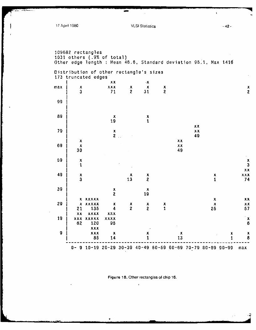
17 April 1980 VLSI Statistics -42-
109682 rectangles1031 others (.9% of total)Other edge length : Mean 46.6, Standard deviation 95.1, Max 1416
Distribution of other rectangle's sizes173 truncated edges
xx -Xmax x xxx x x x x
3 71 2 31 2 2
99
89 x x19 1
I xx79 x xx
2. 49x xx
69 x xx30 49
59 x x1 3
I xx49 x x x x xxx
3 13 2 1 74
39 x x2 19
X xxxxx X xx29 x xxxxx x x x x x xx
21 135 4 2 2 1 25 57xx xxxx xxx
19 xxx xxxxx xxxx x62 120 95 6
xxx9 xxx X X x X X
85 14 1 13 1 8
0- 9 10-19 20-29 30-39 40-49 50-59 60-69 70-79 80-89 90-99 max
Figure 18. Other rectangles of chip 16.

17 April 1980 VLSI Statistics -4.3-
V. Placement HistogramsIn this appendix we present histograms that describe the placement of rectangles over the chip
area. The primary histograms are contained in Section V.1; these histograms describe the two-
dimensional structure of the data. One-dimensional histograms in Section V.2 provide a view of the
data useful in the analysis of the algorithm in Section 3.1.
V.1 Two-dimensional HistogramsThe histograms of this section describe the two-dimensional placement of the rectangles on the
chip. Figure 19. for example describes chip 11. As stated on the figure. that chip contains 1614
rectangles. It was divided into 50X-by-50A squares (from the "50L" in the figure. and the number of
rectangles overlapping each square is denoted by the height of the horizontal lines in the square. The
maximum number of rectangles overlapping any square was 147 (so denoted on the figure); a square
half-full of horizontal lines therefore overlapped approximately 75 rectangles.
The histograms of Figures 19 through 24 show that the rectangles are definitely not distributed
uniformly over the chip: there are large sparse regions around the edges (where there were usually
pads or blank space), and very dense portions in the center of the chip. Indeed, the rectangles are.1more than uniform" over the large, dense portions of the chip -- that is, the variance is less than
expected for uniform random distributions. This observation is quite consistent across all chips: there
is a great deal of sparsity around the edges, and most of the rectangles are distributed uniformly over
portions of the internal part of the chip.

17 April 1980 VLSI Statistics -44-
4. Ii 4
+ +
+I
+ +i
111111 ' ''
+ +
.4.
.4 -4 4 4. 4. 4. 4. 4. 4- 4. 4. 4. 4. 4- 4- . 4. 4. 4- . 4. 4.4.
Bin size: 50A; 16194 rectangles; Max in bin: 147
Figure 19. Placement histogram of chip 1 1.
+
....+ ... . . . .. . . . ' i l l . . . . . . . .... .I I1 : ... . . . . . . -- . . ' -

17 Apjril 1980 VLSI Statistics .45.-
44*4. + . 4- 4 -11 +. + 4. 4. 4. .4. 4.
4..
4. 4
.. 4.
4. 4
4. 4.
4. 4.
+.
4 4.
4 -4-
4. 4b
Bi sie40.765rcage;Ma nbn 5
Fiur 20. _ __ _ Plcm n.hsormofci.2

17 April 1980 VLSI Statistics -46-
+ 4. + 4 . 4. 4. 4. + ++.
+ 'I4. I I
I lI I r -
4.1, Ii 4.
4-;4.
H- I 4.
+ +I
:14. I4.4. II4.
+ +
4. I 4
4.I 1 4.
4. I 4.
4- 4.
+ +I+
+ +
4. 4 . 4. 4 . 4. 4 . 4. 4 . 4 4. 4
Bin size: 50)L; 18056 rectangles: Max in bin: 224
Figu re 21 . Placement histogram of chip 13.
•+
+
+ + . .. . . . . . . . li. . . . . .I .. .I I H '. .

17 April 1980 VLSI Statistics 47-
4+ +
nit ' 1H j1 , 4.
4- I ! 4-
4-I 4
+ +
1 11 1 1111+ +
1 11 11 1 11
4+
+ 1 1 1 H +
II-Ii I! 11111+- +
+ +
1111i1111
111 1= II ..44
,111 4"
1W 1 I f !1I I 4.I
' - 4-
I 4 1 i n ,I,1 1 4-
Bin size: .5O ; 3.3387 rectangles: Max in bin: 173
Figure 22. Placement histogram of chip 14.

17 April 1980 VLSI Statistics - 48.
.. 4 4- 4 4. . . . . . . . . +. 4
+ +
+ +
1 +
4. 4-.
+- +
.
+
4. 4-
+ +
I+
+ +
4. 4.
+, +
S.4 . 4. . . . 4. . . . . . 4 ..
Bin size: lOOX; 95901 rectangles; Max in bin: 768
Figure 23. Placement histogram of chip 15.

17 April 1980 VLSI Statistics -49-
4++ 4" + + + + + + .- .- . . . . .-4 4
4 +
4- 4
+' +
+ 1+
+ +
4.4
+
4-
b 4.
4- +
+ +
+ +
+ +
+ 4-
4 +
4 +
+ +
Bin size: 100 . 109682 rectangles, Max in bin: 740
Figure 24. 0 lacemnent histogram of chip 16.
+ +'
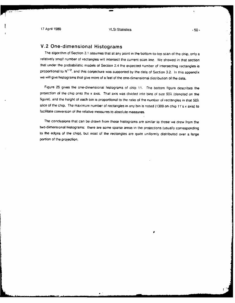
17 April 1980 VLSI Statistics .50 -
V.2 One-dimensional HistogramsThe algorithm of Section 3.1 assumes that at any point in the bottom-to-top scan of the chip, only a
relatively small number of rectangles will intersect the current scan line. We showed in that sectionthat under the probabilistic models of Section 2.4 the expected number of intersecting rectangles isproportional to N 1 2, and this conjecture was supported by the data of Section 3.2. In this appendixwe will give histograms that give more of a feel of the one-dimensional distribution of the data.
Figure 25 gives the one-dimensional histograms of chip 11. The bottom figure describes theprojection of the chip onto the x axis. That axis was divided into bins of size 50A (denoted on thefigure), and the height of each bin is proportional to the ratio of the number of rectangles in that 50Aslice of the chip. The maximum number of rectangles in any bin is noted (1309 on chip 1 il's x axis) tofacilitate conversion of the relative measures to absolute measures.
The conclusions that can be drawn from these histograms are similar to those we drew from thetwo-dimensional histograms: there are some sparse areas in the projections (usually correspondingto the edges of the chip), but most of the rectangles are quite uniformly distributed over a large
portion of the projection.

17 April 1980 VLSI Statistics -51 -
0 0
0 0
0 ~
0 0 lb4iltExHxn x
oIo I I 111111110)1
x x
4.
(0 C1I
Figure 2 5. Projected placement histograms of ch ip I.

17 April 1980 VLSI Statistics -52-0" -
0 0
o 0
0
0) 0)
i-
° I]
o H i
N N
(D (o 01
(n1 (I1
xo 0
x x
0 I
JJ
Figu re 26. Projected placement histograms of chip 12.
B-' '*

17 April 1980 VLSI Statistics .53.
CL Ci'l0 0~N*I~'
II C Ii~~i[
N N ~ 1,
CD C
x x
T T"
Figure 27. Projected piacement histograms of chip 13.

17 April 1980 VLSI Statistics -54-
0 0
o 1111111 S 11xX
x xI a'0 IllhllhlI-. [
0- 1111 o-
N N
*, 0 ~h,
F F
(A) (1Fiur 2tip1
.21,
- lllllAll
ll"lllh"hl"'hIillIhlllhlii[
Figu re 28. Projected placement histograms of chip 14.

17 April 1980 VLSI Statistics -55.
Ct Ct
0 0
Ct Ct0 0x
x x
N N
17-
(D C
x x
Ct CD0D N
Fiue2.Poetdpaeethsorm fci 5

17 April 1980 VLSI Statistics -56-
0 0
0 0
0 011...
0 I Ct
x0
x I.. 111
N N
0 0
N NT T
:3 :3
CIDi
Figure 30. Projected placement histograms of chip 16.
F r. .,

17 April 1980 VLSI Statistics -57-
V1. Data on Rectangle AreaThe measurements presented in Section 2.2 focussed on the number and the edge lengths of
rectangles of certain types. These statistics were used in designing the algorithm of Chapter 3.
Different applications will require additional statistics: in this appendix we present measurements of
more general interest. One of the most important aspects of a layout is area usage. How does the
space devoted to computation compare to the space devoted to communication? What percentage of
the area is used for pads to communicate with the outside world? It is the aim of a good layout to
minimize communication costs; how well can this be achieved?
Table 7 contains area-usage measurements for the 16 chips we studied. The first two columns are
repeated from Table 1 of Section 2.2. The next three columns describe the area used in the chip as a
whole. The column latLieled '88' gives the total area of the chip's bounding box, in units of kilo-X2.
The next column, labeled 'Rects', gives the total area occupied by the rectangles, also in kilo-A2 units.
This column is just the sum of the areas of all rectangles on the chip: thus, if a particular A-by-A
square of the chip is covered by five rectangles, it is counted five times in thiz. measure. The ratio of
these two total area measures is given in the fifth column. For example, columns three through five of
row one say that chip 1 has a bounding box area of 909.000X 2 and a total rectangle area of
841 ,000,\ 2, making the ratio of bounding box area to rectangle area 93. The remainder of the table is
devoted to an area breakdown according to the rectangle trichotomy introduced in Section 2.2. The
'Area' column under 'Components' lists the total area occupied by components (sum of the areas of
all individual components); the next column gives the percei~tage of the total rectangle area this
represents. The columns for wires and others are similar.
The following table summarizes the percentage columns (columns seven, nine and eleven) in Table
7.Median Mean S.D.
Component area % 19.0 19.6 5.0Wire area % 38.5 37.4 6.1Other area % 43.5 43.1 9.2
That is. of the sixteen component-area percentages. the median is 19.0%, the mean, is 19.6% and the
standard deviation is 5.0%. The summary shows that the area percentage breakdowns are quite
consistent across the sixteen designs. with low standard deviations and good agreement between
means and medians. This consistency is rather surprising, given that the chips all had different
designers and that they implemented designs for widely varying applications.
The above data demonstrates the high cost of communication on a chip. On the average, less than
20% of the total rectangle area was devoted to the active components: close to 40% was used for
on-chip communication; slightly over 40% was used for off-chip communication (pads). The designs

17 April 1980 VLSI Statistics -58-
Chip #Total Area Components Wires Others# Rects BB Rects 68/Rects Area % Area % Area %
1 10803 909 841 .93 102 12.1 269 32.0 471 55.92 11265 939 600 .64 118 19.8 235 39.3 244 40.83 11566 672 877 1.31 141 16.1 255 29.0 481 54.94 11853 975 967 .99 130 13.4 272 28.2 565 58.45 11915 817 658 .81 120 18.3 222 33.7 316 48.06 12063 777 689 .89 119 17.2 338 49.2 232 33.67 12800 728 685 .94 135 19.7 262 38.2 288 42.18 14186 1132 1006 .89 173 17.1 354 35.2 479 47.69 14423 836 735 .88 170 23.2 203 27.6 362 49.210 15097 944 740 .78 168 22.7 274 37.1 297 40.211 16194 1315 1092 .83 179 16.4 423 38.8 490 44.912 17565 770 866 1.13 127 14.7 350 40.4 389 44.913 18056 1014 884 .87 210 23.7 351 39.7 323 36.514 33387 1849 1400 .76 355 25.4 677 48.4 367 26.315 95901 4934 3900 .79 1286 33.0 1614 41.4 1000 25.716 109682 7155 5472 .76 1098 20.1 2158 39.4 2216 40.5
Table 7. Data on Rectangle Area.
we studied were relatively small; hence the large relative area devoted to the pads is not surprising.
Moving down the table from the smallest to the largest designs there is a trend toward lower
percentage of the area used for 'other' rectangles. Chip 16 is an exception to this rule; on the other
hand, it has an unusually large number of pads (49). Larger designs. which perform more
computation, can amortize the high cost of the pads more effectively.
The ratio of bounding box area to total rectangle area has mean and median both about .88, with a
standard deviation of .15. These chips were designed with little emphasis on optimal space utilization,
and et hereis ubstntil reulaity n tis rtio

UTJICLASSIFTrDSECURITY C;..ASSi
r 4 3 " T- S PA',E '-,.,ho ".. O.-rd)
REPORT DOCU:.,ENTATIN PACE READ N;S7R"CT:ONS,EORE Cz'AL_,-:'E:x3 FM'.:
-. GOVT ACCESSIO. NO. 3. CIINT'S CAT ALOO N..U8 .i km --C S -6 i l 7 74. TITLEr (andf Sublt!*) S. TYPE OF REPORT & PERIOD COVERED
STATISTICS ON_ I DESIGNS 'lj Interin irC
S. PERFORMING ORG. RA-EORT NUMBER
7. AuT.ORfe) . CONTRACT OR GRANT NUJMSER(')
;ON LOUIS BENTLEY
DOROTHEA HAKEN & ,OBERT W.'/_ON i' 4-76-C-0370.
9. PERFORMING OqGANIZATION NAME AND ADDRESS ;0. PRO RAM ELE.MENT.P;ROJFCT. TASK
Carnegie-Mellon University AREA ' 1K u.NI uBECRsComputer Science Department- __
Pittsburgh, PA 15213
$I. CONTROLLING OFFICE NAME AND ADDRESS -1-A-4 PIaAX, -ATE
Office of Naval Research 'iPR
Arlington, VA 22217 1. AUMER OF PAGES61
14. MONITORI . ENC. -RNE"A-Xr*"RESS(lt d f ont dora ControLling GI .1c) IS. SECURITY CLASS. (of thi .. Pot,)
* Lz- NCLASSIFIEDil[|SO. DECLASSFICATION. ZOiNGRACNG
SCHEDULE
1. DISTRIBUTION STATEAENT (of Itha Report)
Approved for. public release; distribution unlimited
17. DISTRIBUTION STATEMENT (o the abstract entered in Block 20. it dilerent from Report)
IS. SUPPLEMENTARY NOTES
It. KEY WORDS (Cj qtlnu* an reverse io ai ncee/ol. and identify by block numb.)
20. ABSTRACT (Conlinue aI 600re l* ode it necesee l, mid IentlIfy by block n bee)
DD , 1 1473 eoiTION OF I NOV 6S IS ODSOLETE ntiCISSIFIED
SECURITY CLAS.IFICATION OF THIS P&GE (When Does Bn'eorE
So 01