architecture - california institute of · web viewphysiologists use the word...
TRANSCRIPT

Architecture
The architecture of the has evolved to strike the best balance of FPGA resources and algorithm performance while still having design flexibility. The individual voxel processor mapped elegantly to a small cluster of FPGA logic, called the processing element (PE). Interconnections both on-chip and off-chip are orthogonal and therefore map well to island-style FPGA routing and chip array board layout.
3.1 The systolic array
The nature of the iterative solver in the tomography engine is easily parallelized. As soon as input data become available, calculations can be performed concurrently and in-place as data flows through the system. This concept was first defined by Kung at Carnegie-Mellon University:
A systolic system is a network of processors which rhythmically compute and pass data through the system. Physiologists use the word “systole” to refer to the rhythmically recurrent contraction of

the heart and arteries which pulses blood through the body. In a systolic computing system, the function of a processor is analogous to that of the heart. Every processor regularly pumps data in and out, each time performing some short computation, so that a regular flow of data is kept up in the network. [8]
At first, systolic arrays were solely in the realm of single-purpose VLSI circuits. This was followedbyprogrammableVLSI systolicarrays[3] and single-purpose FPGA systolic arrays [2]. As FPGA technology advanced and density grew, generalpurpose “reconfigurablesystolicarrays” [5] couldbeputinsingleor multipleFPGA chips. The capability of eachprocessing elementin earlyFPGA systolic array implementations was limited to small bit-level logic. Modern FPGA chips have large distributed memory and DSP blocks that, along with greater fabric density, allow for word-level 2’s complement arithmetic. The design goals for our systolic array are:
reconfigurable to exploit application-dependent parallelisms high-level-language programmable for task control and flexibility scalable for easy extension to many applications capable of supporting single-instruction stream, multiple-data stream(SIMD)
organizations for vector operations and multiple-data stream(MIMD) organizations to exploit non homogeneous parallelism requirements[6]
Because of system tasks, such as multiple 2-D DFTs per “system

cycle,” the number of compute operations drastically outnumber the I/O operations, and the system is therefore “compute-bound”[7]. The computational rate, however, is still restricted by the array’s I/O operations that occur at the array boundaries. The systolic array tomography engine is composed of many FPGA chips on multiple boards.
The advantages of systolic arrays include reuse of input data, simple and repeatable processing elements, and regular data and control flow. At the same time input data can be cycling into the array while output data is flowing out. At another point calculated data can be flowing. Each individual processing element can only grab and use the data that are presented to it from its nearest neighbors or in its local memory on every clock. This chapter will start at the lowest level of the architecture, the processing element (PE), and gradually zoom out to a system-level perspective.
3.2 The processing element (PE) The heart of our processor is the Xilinx DSP-48 multiplier / accumulator. This is a very powerful cell, which can perform 18-bit pipelined operations at 500MHz. Each processing element uses two of these for the complex arithmetic of the Fourier transform. A single FPGA chip can have over 500 of these cells and allows us to have over 250 PEs per chip.This is the power of the FPGA. While each chip might only be processing data at 100 MHz, each chip contains 250 processors for a
combined processing capability of 25 G Operations per second.
Figure3.1:TheDSP48E architecture[14]

Figure3.2:A single processing element(PE)
Two DSP48s are employed, one for the real and one for the imaginary part of the complex number. As shown in Figure 3.2, the PE also contains a dedicatedBlockRAM memory, an18-bit registerfor the realpart, and an18-bit register for the imaginary part. Multiplexors control whether these registers receive data from their respective MACC or if data are just snaked through them to the next PE. Note that there is only a single 18-bit input and single 18-bit output. This is because when data is flowing through the mesh, the real part is transferred on even clock edges and the imaginary part on odd edges. This is particularly important for instructions types such as the DFT where complex multiplication is performed on inputs split across two clock cycles.

3.3 PE interconnect
The switching lattice for a single 3x3 layer of the SATE is shown in Figure 3.3. For a large telescope this lattice could be 60x60 or larger. The individual PEs are labeled by their column and row position in the mesh. Each PE has a multiplexor onitsinputto routedata orthogonallyfrom a neighboringhorizontal PE, vertical PE, or next layer PE. External I/O only takes place at the mesh boundary on the right and left sides. Information shifts in a circular fashion along columns, rows, or layers. All data paths are 18-bits wide to match the fixed 18-bit inputs of the DSP48E block.
= Output to layer above = Input from layer below


Figure 3.4: Chip bandwidth chart
3.3.1 I/O bandwidth
In the multi-chip system, an important question is how many PEs can be partitioned for each chip. The system has I/O bandwidth requirements that outweigh all other resource requirements. In Figure 3.4, I/O requirements and resource availabilityfor the threeVirtex5SXFPGAs are compared. In order to meet thebandwidth requirementsfor a reasonable number ofPEs on a chip, on-chip multi-gigabit transceivers willhave tobe used. Itisimportant to notefrom the figure that not all of the DSP48E resources were used because total chip bandwidth runsout at acertainpoint.

InordertouseadditionalDSP48Es, additional techniques will be employed such as fabric serialization/deserialization for the LVDS DDRpairs.
3.4 SIMD system control
Most control signals are single bit control, but some, like the address inputs to the BlockRAM, function as index counters to the stored coefficient data. In addition to fine-grained control at the PE level, control signals also manipulate themultiplexorsattheswitchlatticelevel. These control signalsareglobal and can be issued by a single control unit or by distributed copies of the control unit. The control unit requires very few resources so even if multiple copies are distributed, the cost is minimal. The control communication overhead of larger arrays can also be avoided with a copied control scheme.
3.4.1 Cycle accurate control sequencer(CACS)
When the tomography algorithm was mapped to hardware, we found that the array couldbe controlledbylinear sequences of controlbits, specific clock counts of idle, and minimal branching. A Cycle Accurate Control Sequencer module (CACS), shown in Figure 3.5, was architected to be a best of both worlds solution that would (1)
borrow single cycle latency benefits from finite state machines and(2) useprogrammability aspects of a smallRISC engine. Because the CACS logic consists of only an embedded BlockRAM module and a few counters, it has both a small footprint and a fast operational speed.
The control sequence up counter acts as a program counter for the system. The following types of instructions can be issued from the control BlockRAM: 1 Real coefficient address load: Bit 22 signals the real coefficient up counter to be loaded with the lower order data bits. 2 Imag coefficient address load: Bit 21 signals the imaginary coefficient up counter to be loaded with the lower order data bits. 3 Control sequence address load: Bit 20 and status bits control whether or not a conditional branch is taken. If a branch is to be taken, then the control sequence up counter is loaded with the address contained in the lower order data bits. 4 Idle count: Bit23loads adown counter with a cycle count containedinthe lower order data bits. This saves program space during long instruction sequences where control bits do not have to change on every cycle. When thedowncounterreacheszero,theidleis finished andthecontrol sequence up counter is re-enabled. 5 Control bus change: When the high order bits are not being used for counter loads, the low order bits can be changed cycle by cycle for the control bus registers.
Three types of low level instructions are presented in Figure 3.6 to show how a sample control sequence in a text file is compiled by script into BlockRAM content. First the single bit outputs are defined, then an idle count command creates a pause of “cols*2-1” number

of times. Note that “cols” is a variable dependant on the number of east/west columnsin the systolic array. TheSATE instructions are flexible because they incorporate these variables. Single bit changesaredoneonthesubsequenttwocyclesandfinallythereal andimaginary coefficient counters are loaded.
loop_done
19A low-level sequence compile

3.4.2 Instruction set architecture
The instruction set was built to map the algorithms in the basic loop to the reconfigurable systolic array. First, logic was designed around the fixed Block-RAM and MACC resources with control microcode to support the sequences required by the algorithms. Out of the resulting sequences, groups of common microcode sequences were

identified to form the instruction set. Instructions are simply compound sets of control sequences so newinstructions are simple to add and test. As seen in Table 3.1, instructions aregrouped according to which typeof calculation they perform: multiple calculations, singlecalculations,data movement within the PE, or control counter manipulation.
The instructions are shown in Table 3.2 with their respective result. Most instructions require an address to act upon. The long sequence instructions,
Table 3.1: Instruction types
such as macc layer and dft ew, take a starting address and iterate through the proper number of subsequent addresses on their own.
3.4.2.1 macc layer, macc gstar, and dft ns/ew
The macc layer, macc gstar,and dft ns/ew instructions are all essentially complex multiply-accumulate functions. As data

systolically flow through the data registers of each PE, the complex multiply accumulateis carried outbyincreasing the address index for the coefficient RAM and toggling the subtract signal for the real MACC on every clock edge. This functionality is illustrated in Figure 3.7 where the active data lines are shown in red. The difference between macc layer, dft ns, and dft ew is only in the switch lattice, where a circular MACC is done north/south by dft ns, east/west by dft ew, and through the layers by macc layer.
The timing diagram for an in-place DFT accumulation is shown in Figure
3.8. As alternating real and complex values are shifted into the PE, labeled N and n, respectively, the corresponding coefficients, C and c from the dual-port BlockRAM are indexed. The example is for a 2x2 DFT, where the row DFT (dft ew)iscalculated firstand thecolumnDFT(dft ns)is performed on those results.

The macc gstar instruction is performed once the error has been calculated foreachguide star. A single
complexdatavalueiskeptincirculation sothatit can be continuously
Instruction Result macc layer (addr1) Accum: (addr1)*layer1 data+
(addr2)*layer2 data... macc gstar (addr) Accum: (addr1)*data+(addr2)*
data... Dft ns/ew (addr1) Accum: (dft coeff1)*data1+(dft
coeff2)* data2... macc loopback (addr) Accum: (addr)*data registers square rows Real Accum: (real1)2 +(imag1)2 ... add gstar reals (addr) Real Accum: (addr1)+(addr2)+ ... add reals ns Real Accum: data reg real1 + data
reg real2 + ... add (addr) Accum: Accum+(addr) sub (addr) Accum: Accum-(addr) rd ram (addr) Accum: (addr) Wr ram (addr) BRAM(addr): data registers Wr ram indirect BRAM(Accum[10:0]): data reg real rtshift store (addr) data registers: (Accum[47:0]>
>(addr))[17:0] noshift store data registers: Accum[17:0] advance regs data reg real: data reg imag refresh regs data registers: I/O branch if neg (addr) PC: (addr) if PE[0] Accum is negative ld ramcnt indirect coefficient counters: PE[0]
Accum[10:0] Table 3.2: Instructions

multiply-accumulated by a sequence of values in the RAM, as shown in Figure 3.9. This instruction is used for back propagation, where the Cn2 value is circulated.
3.4.2.2 square rows
The square rows instruction uses the same east/west circular shift thathasbeen previously used for dft ew. The multiplexor in front of the real MACC is used to square and accumulate theincomingdata stream until all columnsin the row have been summed, as shown in Figure 3.10.

Figure 3.9: The macc gstar instruction
24

multiplyingby thesystolicallyflowingdata,themultiplierinstead actsuponlocallyloopbackeddatafrom thePE’s own real andimaginary registers, as shown in Figure 3.12.
3.4.2.5 add and sub
The add and sub instructions either perform a complex addition or a

complex subtraction, respectively, of the accumulator to a value in the RAM. Because theMACC module alwayshas to multiplyby something, wefeed a one constant into each multiplier’s second input. The diagram is shown in Figure 3.13.
3.4.2.6 rd ram
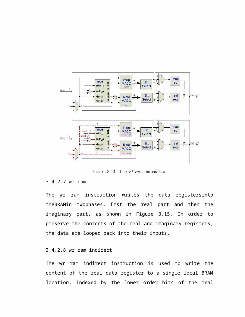
The rd ram instruction first resets the contents of both MACCs. It then loads the real and imaginary counters to a specified memory location where the MACCs multiply-accumulate the data at the given location with the constant one sothatthey nowcontainthedataatthat address, as showninFigure3.14.

27

3.4.2.7 wr ram
The wr ram instruction writes the data registersinto theBRAMin twophases, first the real part and then the imaginary part, as shown in Figure 3.15. In order to preserve the contents of the real and imaginary registers, the data are looped back into their inputs.
3.4.2.8 wr ram indirect
The wr ram indirect instruction is used to write the content of the real data register to a single local BRAM location, indexed by the lower order bits of the real MACC, instead of the usual global counter, as shown in Figure 3.16.

3.4.2.9 rtshift store and noshift store
The“BitSelect”block showninallPEdiagramsisused onlyby the rtshift store and noshift store instructions. By using the rtshift store instruction, the programmer can control how much the 48-bit data that are in the MACCs can be right-shifted before the data are stored in one of the 18-bit data registers. This is useful anywhere wherethesystem needstoscaledowndataby afactorof2x , such as normalization after a DFT. The noshift store instruction simply transfers the lowest 18 bits of the accumulator to the data registers, and therefore uses less cycles. The bit selection logic is shown in Figure 3.17.

3.4.2.10 refresh regs
The refresh regs instruction opens the I/O ports on the mesh boundary and shifts new data in while at the same time shifting results out, as shown in
Figure 3.18. This instruction is used when the SATE has reached convergence and it is ready to accept new measured data from the wavefront sensors.
3.4.2.11 advance regs
The advance regs instruction simply enables the real and imaginary registers for one clock cycle, as shown in Figure 3.19. Data are

looped back into the imaginary register in case they are needed again. For example, two sequential advance regs instruction would return the data registers to their original contents. This is the same concept that preserves the data registers in the wr ram instruction.
3.4.2.12 branch if neg
The branch if neg instruction uses a high order bit from the real MACC in the PE located at row zero, column zero, layer zero to conditionally load the CACSprogramcounter with a newindex value, as showninFigure3.20. If the high order bit is a one, which would

indicate that the accumulator contains a negative value, then the CACS counter is loaded. If the bit is a zero, then the accumulator value mustbepositive so noloadisperformed.
3.4.2.13 ld ramcnt indirect
Like branch if neg, the ld ramcnt indirect instruction uses information from only the first PE, which is at location row zero, column zero, layer zero. The low order bit data from both the real and imaginary MACCs are used to load
PE: row 0, col 0, layer 0
the global real and imaginary coefficient up counters, as shown in Figure 3.21.

3.5 Algorithm mapping
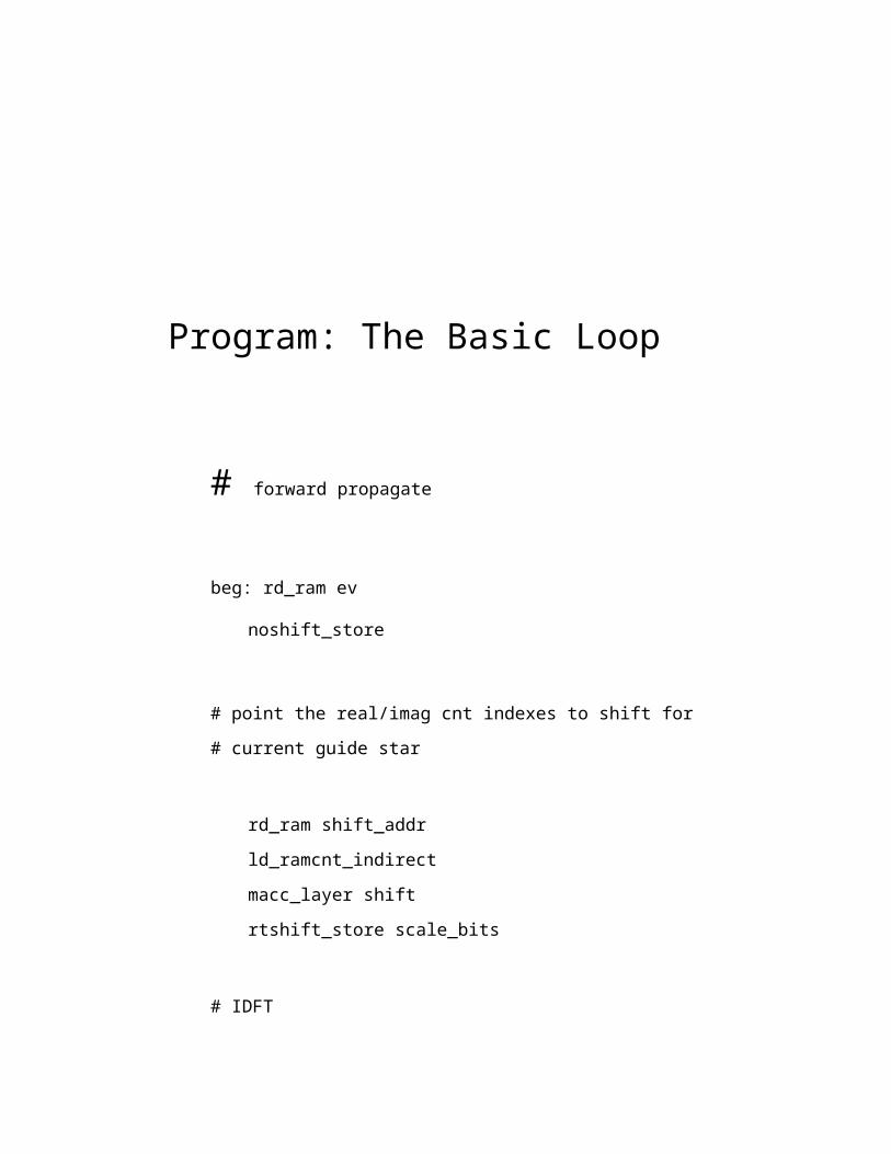
ThebasicloopprogramisshowninFigure3.22. Inthissection, we will explain howthemainpartsof theprogramaremappedintoinstructionsequences. The complete program can be viewed in Appendix A.
1. Forward propagation is performed by a macc layer instruction on shift values for the current guide star.
2. Adjustedforwardpropagationisdonebya dft instruction usingtheinverse dft coefficient set that is stored in RAM.
3. An aperture is taken on the register data by a macc loopback instruction that multiplies the data by 1 or 0, depending on if the PE is inside or outside of the aperture.
4. Error is calculated by first writing the adjusted forward-propagated value to a temporary RAM location. The measured value is subtracted from the adjusted forward value.
5. A dft instruction using the forward coefficients is taken to bring the data back into the Fourier domain.
6. The error is written to RAM to be used later for back propagation. The error address location is loaded and then offset by the current guide star index. Once the correct location is in the real accumulator, register data are written using wr ram indirect.

7. An errormagnitudeistakenby firstsquaring and accumulating along the east/westdirection with square rows. The add reals ns instructionis then used to add the real result of each row in the north/south direction. The final error magnitude for the guide star is written to a specific location using wr ram indirect.
8. The global error is calculated using add gstars reals. This instruction takes the address of guide star error magnitudes and sums them.
9. Back propagation is done by the macc gstar instruction, which takes the errors that were written by step 6 and multiply-accumulates them by the Cn 2 of the layer.

10. Adjusted coefficient error is simply a complex multiplication of the Kolmogorov filter value by the coefficient error.
11. A new estimated value is calculated by adding the adjusted coefficient error to the current estimated value and storing the result in RAM.


Scalability
The system is intended for use on a variety of AO systems. Certain characteristics of the system such as aperture of the telescope will determine the size and shape of the systolic array. The SATE architecture therefore needs to have the capability of being generated according to the traits of the target AO system.
4.1 Centralized definitions
The dimensions of the meshed box are specified in definitions.h. All the Ruby scriptsandVerilog[4] filesreferencethiscentral filefordynamically creating module definitions and memory contents. An example of a definitions file is shownbelowwherethe3-D arrayisspecified as64 columnswide,64 rowsdeep, and 8 layers high:
‘define COLUMNS 64 ‘define ROWS 64‘define LAYERS 8‘define CONN_WIDTH 18‘define RAM_ADDR_BITS 11‘define RAM_WIDTH 18

‘define SCALE_BITS 10
4.2 Verilog architecture generation
For simplicity and usability,Ruby[12] was selectedforVeriloggeneration. The Verilog generate statement was not used because it can not dynamically reference the external memory content files. Each module is explicitly defined with reference to the memory content file that it uses, as shown below for a PE at location column 0, row 3, layer 0:
pe_block #( .FILENAME("c0_r3_l0.data") ) pb_c0_r3_l0 ( .clk(clk), .rst(rst), .load_acc(load_acc), .ce_dsp_real(ce_dsp_real), . . .
); The switch-latticepattern showninFigure3.3 onpage15is alsogenerated according to dimensions defined in definitions.h. Any

system with Ruby installed canrunthescriptsthatgeneratethetoplevelVerilog files top.v and box.v. The hierarchy of architecture files is shown below with their brief descriptions.
1. top.v : top level Verilog interface file (a) box.v : routing and MUXs for switch lattice i. muxer4.v : 4 input MUX with 3 inputs for switch lattice ii. muxer3.v : 4 input MUX with 4 inputs for switch lattice iii. pe block.v : The basic Processing Element A. dsp e.v :AVerilog wrapper fileforXilinxDSP48Eprimitive B. bram infer.v : Infers the Xilinx BlockRAM primitive for a PE C. bit select.v : A loadable right shifter
(b) cacs.v : The SIMD controller and associated logic
i. brom infer.v : InferstheXilinxBlockRAMprimitiveforprogram memory
4.3 RAM data structure
The static data that each PE needs are calculated before run time and loaded into eachPE’sBlockRAM on configuration. ABlockRAMgeneration script referencesthedefinitions fileand writesamemory content fileforeachBlockRAM in the system. EachparticularBlockRAM containsDFT andIDFT coefficients, aperture values, filter values, constants, as well as some dynamic data, such

as estimated and intermediate error values. In addition to defining the memories, an address map file shows
where data have been placed in all of the memories. The program compiler references this filefor addresskeywords, such as kolm fortheKolmogorov filtervalueorcn2 for the C2 value, as seen below. The smaller data sets are located at low addresses
n
(0 to 99 in the example below) and the large DFT and IDFT coefficients are writtenlast(100 onwardbelow). Itisstraightforwardto add additionaldata sets by modifying the BlockRAM generation script.
shift 0 4cn2 812aperture 16 18kolm 20 22afp 24 25ev 26 27const1 28 30inv_dft 100 164fwd_dft 228 292

This functionality hides the memory mapping details from the programmer. For example, a rd ram cn2 instruction would be compiled to first load the real coefficient up counter (as shown in Figure 3.5) with an 8, and then load the imaginary coefficient up counter with a 12. The instruction then proceeds, as shown inFigure3.14, and the accumulators now contain the real andimaginary C2 values.
n

Verification
TheVerilogsimulationtool oftheSATE systemisModelSimSE[10]. Modelsim-SEis anindustry-provenRTL simulator thatis availabilein theUCSCMicroarchitecture Lab. Xilinx primitives are directly instantiated and simulated in a Modelsim cycle-accurate simulation. Ruby-VPI[9] scriptsdrivetheSATE testbench together with Modelsim.
5.1 Simulation size
The SATE system that will work on real data sets will require an array of PEs numbering in the thousands. Even the most capable desktop systems with behavioralRTL simulators would takehoursif notdaysjust togetthrough a single iteration of the algorithmicloop. But,because the scale of the arraydoes not affect operational validity, a relatively small array canbequickly simulated and the same results would apply to any larger version.

5.2 Performance
The current version of theSATE algorithmuses nopreconditioning intheloop so the estimated values “converge” slowly. It also begins from a cold start so the estimated values start at zero and ramp up. A small 8x8x3 SATE array is adequate enough for verification without consuming unreasonable amounts of memory and CPU time on the simulator desktop computer. Each iteration through the loop takes 1,900 SATE clock cycles.
Verification of the basic iterative algorithm is performed using a fake data set composed of constant measured values for three guide stars. The set of constant values arethe equivalent of therebeing

aperfect atmosphere, and the layer estimate root mean squares should converge to the ratios set by the Cn 2 values of thelayer. InFigure5.1, thethreelayerR.M.S. values roughlyconverge to the samelevel. InFigure5.2, the Cn 2 values are set to ratios of0.6forlayer0,
0.3 for layer 1, and 0.1 for layer 2 of the 65,536 scaling factor. Forty iterations through thebasicloop are shownforbothgraphs.

Implementation
TheXilinxISE9.2tools were usedto synthesize,place, androutetheSATE.The designisfullyfunctional and synthesizable forboth theVirtex4 andVirtex5SX families. To target theVirtex4, the pe block.v file can be changed toinstantiate dsp.v in order to use theDSP48primitivein theVirtex4, as opposed to dsp e.v, which uses the newer DSP48E primitive of the Virtex5.
6.1 Synthesis
Thebuildingblock ofthe systolic arrayisthe singleprocessing element(PE). As the PE was first defined and later redefined (as instructions were added), the concept of“design for synthesis” was always employed. Every piece of RTL codeislogically mappedbythedesigner tointendedFPGA resources. Therefore the synthesis tool does not have to fill in any blanks when it is inferring what resources to use. Table 6.1 shows utilization numbers in a Virtex5 device for a single PE:

6.2 Place and route
AVirtex5SX95TFPGA wastargeted with a4x4x3 array. Timing closurewas achieved at 150MHz. The Post-PAR utilization summary is shown below. The first resource to run out is I/O. Future work on the SATE will have to involve serialization strategies using device fabric and dedicated Serializer-Deserializer (SERDES)primitives.
Device Utilization Summary:Number of BUFGs 1 out of 32 3%Number of DSP48Es 96 out of 640 15%Number of External IOBs 436 out of 640 68%Number of LOCed IOBs 0 out of 436 0%Number of RAMB18X2s 49 out of 244 20%Number of Slice Registers 6981 out of 58880 11%Number used as Flip Flops 6981

Number used as Latches 0Number used as LatchThrus 0
Number of Slice LUTS 11663 out of 58880 19%

Other Issues
7.1.1 Designing for multi-FPGA, multi-board
A complete SATE system ready to be integrated into an adaptive optics system would contain 64 rows, 64 columns, and 5 layers. As shown in Figure 3.4 onpage onpage16,iftheSX95TFPGA(147PEs) is selected(64 x64 x5 = 20480 PEs), then at least 140 FPGAs are needed. Each FPGA needs to communicate with its neighbors to its immediate north, south, east, and west. The optimal number of PEs on-chip will be a balance of system-wide communication bandwidth, power, and I/O limitations for PCB and cable. On-chip high-speed SERDES components will be used to ensure that total bandwidth rates through the entire array are optimal. The elimination of long wires at row or column boundaries will be done by folding at board edges and/or torus optimal placement techniques.
7.1.2 Unused FPGA Fabric
Becausethe system employs many powerful FPGAs, the capabilityofthe system can always be improved, even after complete boards are assembled. Currently, mostofthelogicutilizationisinthe

fixed resourcesoftheVirtex5(DSP48Es and BlockRAM). Much FPGA fabric is left unused. Potential uses include:
1. The CACS control logic could be duplicated to improve timing toward a higher system clockfrequency. Multiple copies of the controllogic on-chip would reduceboth the criticalpathlength of controllines as well asfanout for those nets. If each chip has control logic, then the control nets do not have to be passed to other chips, which saves I/O pins.
2. Forthebest visibility, moderntelescopes areplacedinhigh altitudelocations. Theselocations are more vulnerableto a single event upset(SEU). An SEU is a change of state caused by a high-energy particle strike to a sensitive node in a micro-electronic device. The ability to detect a problem and rapidly fix it is critical because the operation of the whole telescope is expensive so repeating an observation that lasts many hours is extremely costly. CRC logic could be built to verify validity of static BRAM contents while the system is in operation. The static contents could be reprogrammed with partial reconfiguration techniques while the system is still operating.

Appendix A

Program: The Basic Loop
# forward propagate
beg: rd_ram ev
noshift_store
# point the real/imag cnt indexes to shift for# current guide star
rd_ram shift_addrld_ramcnt_indirectmacc_layer shiftrtshift_store scale_bits
# IDFT

dft_ew inv_dft_ewrtshift_store scale_bitsdft_ns inv_dft_ns
# in addition to scaling down, also normalize down here
rtshift_store normalize_bits
# take aperture in spatial
macc_loopback aperturenoshift_store
# take error in spatial
wr_ram temprd_ram meas_addrld_ramcnt_indirectrd_ram_directsub tempnoshift_store

# move spatial error to Fourier with DFT
dft_ew fwd_dft_ewrtshift_store scale_bitsdft_ns fwd_dft_nsrtshift_store scale_bitswr_ram error_temp
# write error for this guidestar to 4 memory locations# back propagation needs it in this format## procedure: write Real to locations 1 then 2
# write Imag to locations 3 then 4# 1.) error_addr : R# 4.) error_addr+1 : I#.#.# 3.) error_addr + 2x#gstars : I# 2.) error_addr + 2x#gstars + 1 : R
rd_ram error_addr
# writes to 1.
wr_ram_indirectadd gstar_numadd gstar_numadd unscaled_const1
# writes to 2.
wr_ram_indirectadvance_regssub unscaled_const1
# writes to 3.
wr_ram_indirectsub gstar_numsub gstar_numadd unscaled_const1

# writes to 4.
53 wr_ram_indirect
# put the error_addr at location for next gstar (in case we come back here)
add unscaled_const1noshift_storewr_ram error_addr
# get an error magnitude for this guide star
rd_ram error_tempnoshift_store
# square_rows accumulates all R^2 + I^2 values in each row in the real accum

square_rows
# scale down the sum of square rows, this incurs some roundoff errors*
rtshift_store scale_bits
# add_reals_ns accumulates the real values north/south# in a real path only, bypassing the imag paths
add_reals_ns unscaled_const1noshift_store
# writes to proper sum of squares location: (sos_addr + gstar_cnt)
rd_ram sos_addradd gstar_cntwr_ram_indirect
# increase meas address index

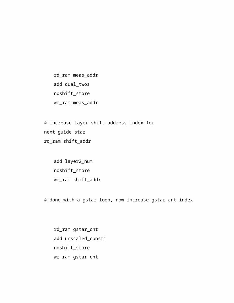
rd_ram meas_addradd dual_twosnoshift_storewr_ram meas_addr
# increase layer shift address index for next guide starrd_ram shift_addr
add layer2_numnoshift_storewr_ram shift_addr
# done with a gstar loop, now increase gstar_cnt index
rd_ram gstar_cntadd unscaled_const1noshift_storewr_ram gstar_cnt

sub gstar_num
# if we haven’t gotten an error for each guide star,# branch to the beginning
branch_if_neg beg
# determine if global error is small enough to exit program# sum the sum of squares values across all guide stars
add_gstar_reals sossub cutoff
# here is the bailout condition
branch_if_neg stop
# Back Propagation
rd_ram cn2noshift_storemacc_gstar error

rtshift_store scale_bitsmacc_loopback unscaled_const1
# Kolm filter
macc_loopback kolm
# new estimated value
add ev noshift_storewr_ram ev
# we are at end of loop so reset address indexes for:# gstar_cnt,
rd_ram const_zeronoshift_storewr_ram gstar_cnt
# meas_addr,
rd_ram meas_addr_startnoshift_storewr_ram meas_addr
# shift_addr,
rd_ram shift_addr_startnoshift_storewr_ram shift_addr
# error_addr,
rd_ram error_addr_startnoshift_storewr_ram error_addr
# now force a branch to the very beginning of loop
rd_ram neg_constbranch_if_neg beg

stop: done


Appendix B
Framework Requirements
B.1 GenerateVerilogfiles,BlockRAMcontents, and
program compilation
1 Ruby 2 NArray library for Ruby
B.2 Behavioral RTL simulation
1 Linux OS 2 Ruby 3 NArray library for Ruby 4 Ruby-VPI 16.0.0 or higher that works with ModelSim 5 Modelsim SE Simulator 6 Xilinx primitive libraries for Modelsim SE


Appendix C
Ruby scripts
C.1 Ruby scripts for Verilog Generation
1 gen top.rb : generates the top level Verilog file: “top.v” 2 gen box.rb : generates the 3-D systolic box Verilog file: “box.v”
3. gen all.rb:callsall architecturegenerationscripts,oneat atime(“gen top.rb”, “gen box.rb”, “gen all.rb”)
C.2 Ruby scripts for systolic array BlockRAM
content generation

1. gen mesh brams.rb : ← uses functions located in “gen bram functions.rb” ← generates the BlockRAM content files: ”c# r# l#.data” ← generates the address file: “addr.data”
C.3 Ruby scripts for CACS program compilation
1 compile.rb : compiles any sequence list text file into “whole sequence.seq” 2 gen cacs rom.rb : compiles whole sequence.seq into the final CACS rom file : “control rom.data”.


References
[1] D. Gavel. Tomography for multiconjugate adaptive optics systems using laserguide stars. SPIEAstronomicalTelescopes andInstrumentation,2004.
[2] M. Gokhale. Splash: A Reconfigurable Linear Logic Array. Parallel Processing, International Conference on, pages 1526–1531, 1990.
[3] R. Hughey and D.P. Lopresti. Architecture of a programmable systolic array. Systolic Arrays, Proceedings of the International Conference on, pages 41–49, 1988.
[4] IEEEComputerSociety.IEEEStandardforVerilogHardwareDescription Language. Std. 1364-2005, IEEE, 7 April 2006.
[5] K.T. Johnson, A.R. Hurson, and Shirazi. General-purpose systolic arrays. Computer, 26(11):20–31, 1993.
[6] A.KrikelisandR.M.Lea.Architecturalconstructsforcost-effectiveparallel computers. pages 287–300, 1989.

[7] H.T. Kung. Why Systolic Architectures? IEEE Computer, 15(1):37–46, 1982.
[8] H.T.Kung andC.E.Leiserson. SystolicArrays(forVLSI). Proceedings of Sparse Matrix Symposiums, pages 256–282, 1978.
[9] Kurapati. Specification-driven functional verification with Verilog PLI & VPI and SystemVerilog DPI. Master’s thesis, UCSC, 23 April 2007.
[10] Mentor Graphics Corporation. ModelSim SE User’s Manual, software version 6.3c edition, 2007.
[11] M. Reinig. The LAO Systolic Array Tomography Engine. 2007.
[12] D. Thomas, C. Fowler, and A. Hunt. Programming Ruby: The Pragmatic Programmer’sGuide. PragmaticBookshelf,Raleigh,NorthCarolina,2005.
[13] W.M. Keck Observatory. The Next Generation Adaptive Optics System: Design and Development Proposal. 2006.
[14] Xilinx, Inc. Virtex-5 XtremeDSP Design Considerations User Guide,7 January 2007.