ars.els-cdn.com · web viewtest results of reverse scan and forward scan for sno 2 based devices...
TRANSCRIPT
Supporting Information
Stacking n-type layers: effective route towards stable, efficient and
hysteresis-free planar perovskite solar cells
Xueping Liua1, Tongle Bua1, Jing Lia, Jiang Hea, Tianhui Lia, Jun Zhangb, Wangnan Lic, Zhiliang
Kua, Yong Penga, Fuzhi Huanga, Yi-Bing Chenga,d and Jie Zhonga*
a State Key Laboratory of Advanced Technology for Materials Synthesis and Processing, Wuhan
University of Technology, Wuhan 430070, PR China
b Wuhan National Laboratory for Optoelectronics, Huazhong University of Science and
Technology, Wuhan 430074, PR China
c Hubei Key Laboratory of Low Dimensional Optoelectronic Materials and Devices, Hubei
University of Arts and Science, Xiangyang 441053, PR China
d Department of Materials Science and Engineering, Monash University, VIC 3800, Australia
*Corresponding Email: [email protected]
1 These authors contributed equally to this work.
Table S1. Detailed J-V test results of reverse scan and forward scan for the SnO2
based devices.
Concentration Thickness Voc [V] Jsc [mA/cm2] FF PCE [%]
150 mg/mL 100 nm 1.109 20.43 0.550 12.47
75 mg/mL 50 nm 1.089 20.67 0.649 14.62
50 mg/mL 30 nm 1.067 20.55 0.735 16.12
37.5 mg/mL 18 nm 1.078 21.85 0.737 17.35
30 mg/mL 12 nm 1.098 21.11 0.716 16.60
25 mg/mL 8 nm 1.119 20.47 0.627 14.36
18.8 mg/mL 5 nm 1.055 19.90 0.627 13.16
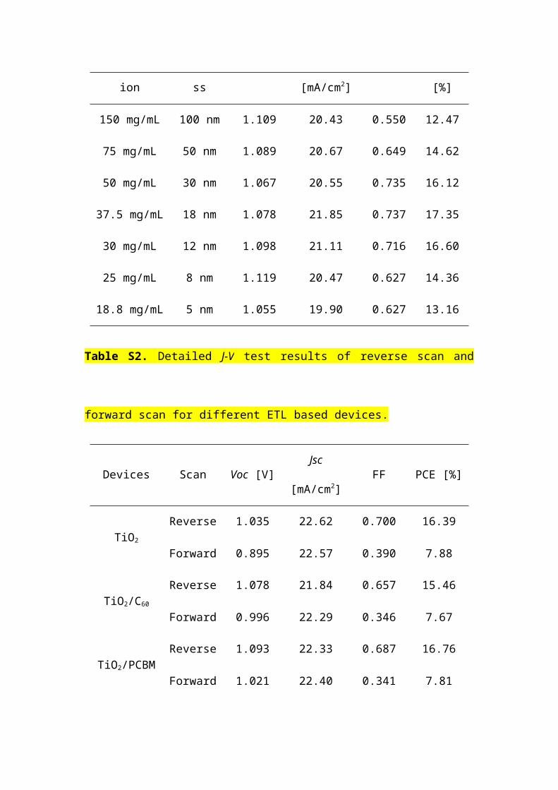
Table S2. Detailed J-V test results of reverse scan and forward scan for different ETL
based devices.
Devices Scan Voc [V]Jsc
[mA/cm2]FF PCE [%]
TiO2Reverse 1.035 22.62 0.700 16.39Forward 0.895 22.57 0.390 7.88
TiO2/C60Reverse 1.078 21.84 0.657 15.46Forward 0.996 22.29 0.346 7.67
TiO2/PCBMReverse 1.093 22.33 0.687 16.76Forward 1.021 22.40 0.341 7.81
SnO2Reverse 1.080 21.55 0.694 16.15Forward 1.058 21.55 0.716 16.34
SnO2/C60Reverse 1.064 19.55 0.632 13.15Forward 1.046 19.97 0.529 11.06
SnO2/PCBMReverse 1.082 20.76 0.641 14.39Forward 1.088 20.63 0.703 15.77
Table S3. Detailed J-V test results of reverse scan and forward scan for SnO2 based
devices with 30 , 150 and 300 annealing.℃ ℃ ℃
Devices Scan Voc [V]Jsc
[mA/cm2]FF PCE [%]
SnO2 30℃Reverse 1.059 20.87 0.620 13.70Forward 1.074 20.97 0.680 15.31
SnO2 150℃Reverse 1.123 20.63 0.739 17.12Forward 1.119 20.56 0.700 16.10
SnO2 300℃Reverse 1.060 20.52 0.614 13.36Forward 1.061 20.62 0.631 13.82
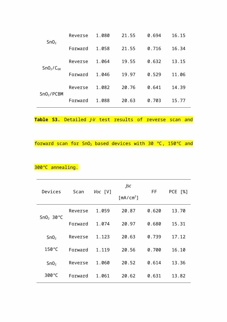
Figure S1. The J-V curves of the devices with SnO2 ETLs processed using different
solid concentration.
Figure S2. (a-c) SEM images of TiO2, SnO2, and stacked n-layer films, respectively.
Figure S3. (a-c) AFM images of TiO2, SnO2, and stacked n-layer films, respectively.
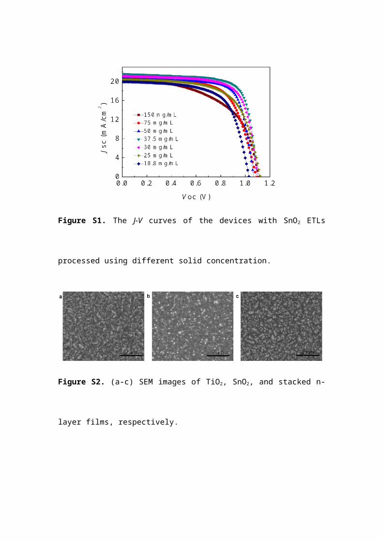
Figure S4. (a) J-V curves of the TiO2, TiO2/C60-SAM, TiO2/PCBM based devices
under reverse and forward voltage scan. (b) J-V curves of the SnO2, SnO2/C60, and
SnO2/PCBM based devices under reverse and forward voltage scan.
Figure S5. The absorbance of TiO2, SnO2, and stacked n-layer based perovskite films.
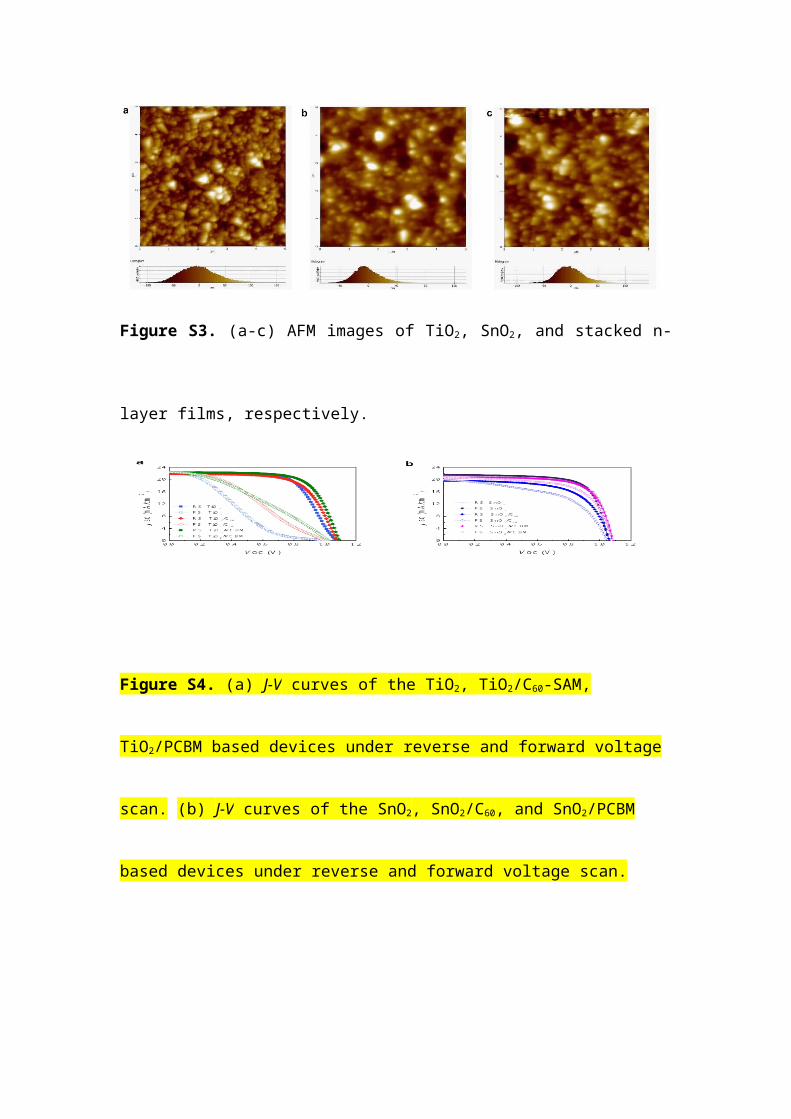
Figure S6. The detailed statistics of Voc, Jsc, and FF decays over time.
Figure S7. X-ray diffraction pattern of SnO2 nanoparticles. The diffraction peaks
from each crystal planes are labelled.
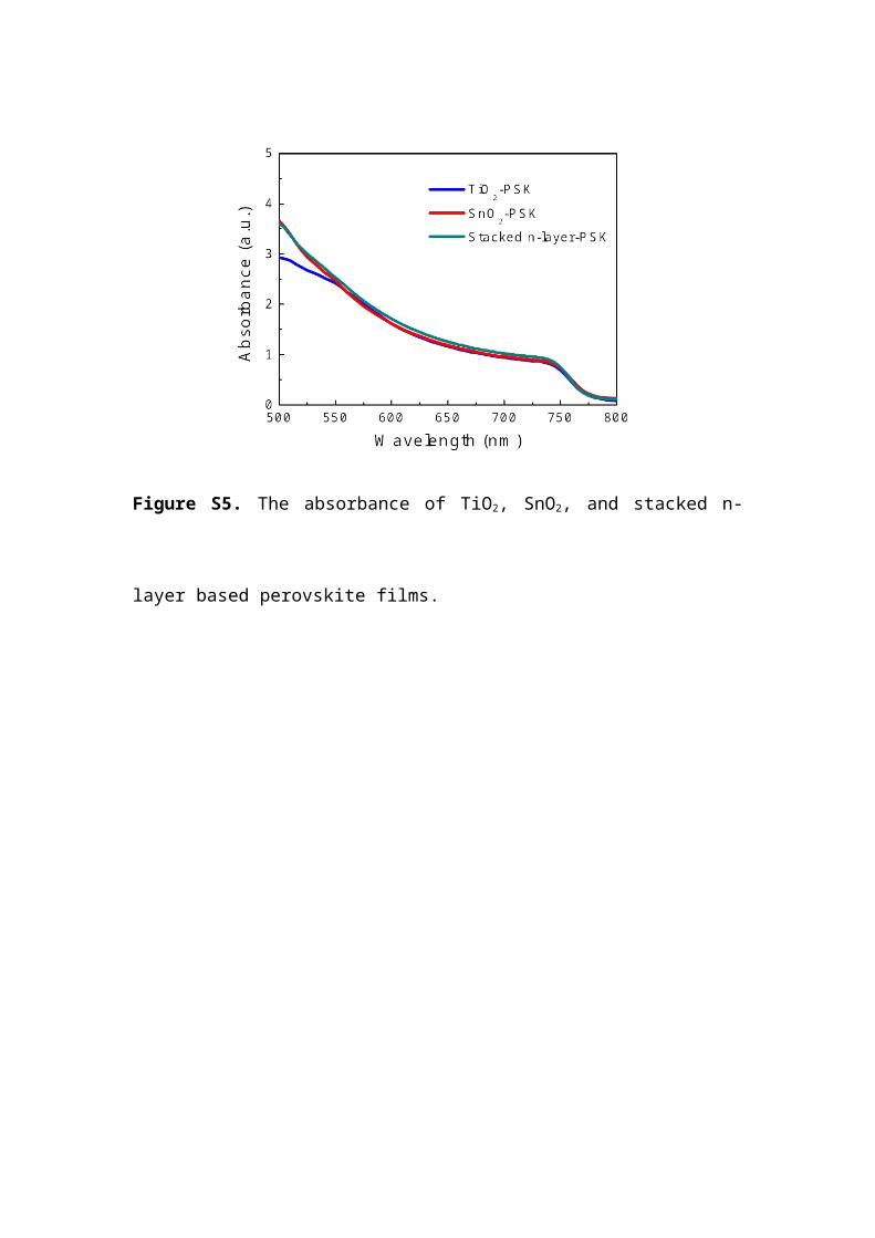
Figure S8. FT-IR of SnO2 at 30 ℃, 150 ℃, 300 ℃, respectively.
Figure S9. Commercial environmental chamber for accelerated stability tests.