asmi parallel ii intel® fpga ip core user guide · asmi parallel ii intel® fpga ip core user...
TRANSCRIPT

ASMI Parallel II Intel® FPGA IP CoreUser Guide
Updated for Intel® Quartus® Prime Design Suite: 18.0
SubscribeSend Feedback
UG-20068 | 2018.09.24Latest document on the web: PDF | HTML

Contents
ASMI Parallel II Intel® FPGA IP Core User Guide................................................................ 3Ports.......................................................................................................................... 4Parameters................................................................................................................. 5Register Map............................................................................................................... 6Operations.................................................................................................................. 8
Control Status Register Operations........................................................................8Memory Operations.............................................................................................9
ASMI Parallel II Intel FPGA IP Core Use Case Examples................................................... 10Example 1: Read the Silicon ID of the Configuration Devices...................................12Example 2: Read and Write One Word of Data at Address H'40000000..................... 12Example 3: Erase Sector 64................................................................................13Example 4: Perform Sector Protect at Sectors (0 to 127)........................................13Example 5: Read and Clear Flag Status Register....................................................13Example 6: Read and Write nvcr......................................................................... 13
ASMI Parallel II Intel FPGA IP Core User Guide Archives.................................................. 13Document Revision History for the ASMI Parallel II Intel FPGA IP Core User Guide...............14
Contents
ASMI Parallel II Intel® FPGA IP Core User Guide Send Feedback
2

ASMI Parallel II Intel® FPGA IP Core User GuideThe ASMI Parallel II Intel® FPGA IP core provides access to the Intel FPGAconfiguration devices which are the quad-serial configuration (EPCQ), low-voltagequad-serial configuration (EPCQ-L), and EPCQ-A serial configuration. You can use thisIP core to read and write data to the external flash devices for applications, such asremote system update and SEU Sensitivity Map Header File (.smh) storage.
Other than the features supported by the ASMI Parallel Intel FPGA IP core, the ASMIParallel II Intel FPGA IP core additionally supports:
• Direct flash access (write/read) through the Avalon®-Memory Map (Avalon-MM)interface.
• Control register for other operations through the control status register (CSR)interface in the Avalon-MM.
• Translate the generic commands from the Avalon-MM into device command codes.
The ASMI Parallel II Intel FPGA IP core is available for all Intel FPGA device familiesincluding the Intel MAX® 10 devices which are using the GPIO mode.
The ASMI Parallel II Intel FPGA IP core only supports the EPCQ, EPCQ-L, and EPCQ-Adevices. If you are using third-party flash devices, you must use the Generic SerialFlash Interface Intel FPGA IP core.
Note: The ASMI Parallel II Intel FPGA IP core is supported in the Intel Quartus® Primesoftware version 17.0 and onwards.
Related Information
• Introduction to Intel FPGA IP CoresProvides general information about all Intel FPGA IP cores, includingparameterizing, generating, upgrading, and simulating IP cores.
• Creating Version-Independent IP and Qsys Simulation ScriptsCreate simulation scripts that do not require manual updates for software or IPversion upgrades.
• Project Management Best PracticesGuidelines for efficient management and portability of your project and IP files.
• ASMI Parallel Intel FPGA IP Core User Guide
• Generic Serial Flash Interface Intel FPGA IP Core User GuideProvides support for third-party flash devices.
• AN 720: Simulating the ASMI Block in Your Design
UG-20068 | 2018.09.24
Send Feedback
Intel Corporation. All rights reserved. Intel, the Intel logo, Altera, Arria, Cyclone, Enpirion, MAX, Nios, Quartusand Stratix words and logos are trademarks of Intel Corporation or its subsidiaries in the U.S. and/or othercountries. Intel warrants performance of its FPGA and semiconductor products to current specifications inaccordance with Intel's standard warranty, but reserves the right to make changes to any products and servicesat any time without notice. Intel assumes no responsibility or liability arising out of the application or use of anyinformation, product, or service described herein except as expressly agreed to in writing by Intel. Intelcustomers are advised to obtain the latest version of device specifications before relying on any publishedinformation and before placing orders for products or services.*Other names and brands may be claimed as the property of others.
ISO9001:2015Registered

Ports
Figure 1. Ports Block Diagram
ASMI Parallel II Intel FPGA IP
reset_n
clk
avl_csr_read
qspi_scein
avl_csr_writedata
avl_mem_write
avl_mem_burstcount
avl_mem_waitrequest
avl_mem_readddata
avl_mem_rddata_validavl_mem_read
avl_mem_addr
avl_mem_writedata
avl_mem_byteenble qspi_dclk
qspi_dataout
avl_csr_write
avl_csr_addr avl_csr_rddata
avl_csr_rddata_valid
avl_csr_waitrequest
Table 1. Ports Description
Signal Width Direction Description
Avalon-MM slave interface for CSR (avl_csr)
avl_csr_addr 6 Input Avalon-MM address bus. The address bus is in word addressing.
avl_csr_read 1 Input Avalon-MM read control to the CSR.
avl_csr_rddata 32 Output Avalon-MM read data bus from the CSR.
avl_csr_write 1 Input Avalon-MM write control to the CSR.
avl_csr_writedata 32 Input Avalon-MM write data bus to CSR.
avl_csr_waitrequest 1 Output Avalon-MM waitrequest control from the CSR
avl_csr_rddata_valid 1 Output Avalon-MM read data valid that indicates the CSR read data isavailable.
Avalon-MM slave interface for memory access (avl_ mem)
avl_mem_write 1 Input Avalon-MM write control to the memory
avl_mem_burstcount 7 Input Avalon-MM burst count for the memory. The value range from 1 to64 (maximum page size).
avl_mem_waitrequest 1 Output Avalon-MM waitrequest control from the memory.
avl_mem_read 1 Input Avalon-MM read control to the memory
avl_mem_addr N Input Avalon-MM address bus. The address bus is in word addressing.
continued...
ASMI Parallel II Intel® FPGA IP Core User Guide
UG-20068 | 2018.09.24
ASMI Parallel II Intel® FPGA IP Core User Guide Send Feedback
4

Signal Width Direction Description
The width of the address depends on the flash memory densityused.
avl_mem_writedata 32 Input Avalon-MM write data bus to the memory
avl_mem_readddata 32 Output Avalon-MM read data bus from the memory.
avl_mem_rddata_valid 1 Output Avalon-MM read data valid that indicates the memory read data isavailable.
avl_mem_byteenble 4 Input Avalon-MM write data enable bus to memory. During burstingmode, byteenable bus will be logic high, 4’b1111.
Clock and Reset
clk 1 Input Input clock to clock the IP core. (1)
reset_n 1 Input Asynchronous reset to reset the IP core.(2)
Conduit Interface(3)
fqspi_dataout 4 Bidirectional Input or output port to feed data from the flash device.
qspi_dclk 1 Output Provides clock signal to the flash device.
qspi_scein 1 Output Provides the ncs signal to the flash device.Supports Stratix® V, Arria® V, Cyclone® V, and older devices.
3 Output Provides the ncs signal to the flash device.Supports Intel Arria 10 and Intel Cyclone 10 GX devices.
Related Information
• Quad-Serial Configuration (EPCQ) Devices Datasheet
• EPCQ-L Serial Configuration Devices Datasheet
• EPCQ-A Serial Configuration Device Datasheet
Parameters
Table 2. Parameter Settings
Parameter Legal Values Descriptions
Configuration device type EPCQ16,EPCQ32,EPCQ64,EPCQ128,EPCQ256,EPCQ512,
EPCQ-L256,EPCQ-L512,EPCQ-L1024,
EPCQ4A,
Specifies the EPCQ, EPCQ-L, or EPCQ-A device type you want touse.
continued...
(1) You can set the clock frequency to lower or equal to 50 MHz.
(2) Hold the signal for at least one clock cycle to reset the IP.
(3) Available when you enable the Disable dedicated Active Serial interface parameter.
ASMI Parallel II Intel® FPGA IP Core User Guide
UG-20068 | 2018.09.24
Send Feedback ASMI Parallel II Intel® FPGA IP Core User Guide
5

Parameter Legal Values Descriptions
EPCQ16A,EPCQ32A,EPCQ64A,EPCQ128A
Choose I/O mode NORMALSTANDARD
DUALQUAD
Selects extended data width when you enable the Fast Readoperation.
Disable dedicated ActiveSerial interface
— Routes the ASMIBLOCK signals to the top level of your design.
Enable SPI pins interface — Translates the ASMIBLOCK signals to the SPI pin interface.
Enable flash simulationmodel
— Uses the flash inside the device for simulation model.
Number of Chip Select used 12(4)
3(4)
Selects the number of chip select connected to the flash.
Related Information
• Quad-Serial Configuration (EPCQ) Devices Datasheet
• EPCQ-L Serial Configuration Devices Datasheet
• EPCQ-A Serial Configuration Device Datasheet
• AN 720: Simulating the ASMI Block in Your Design
Register Map
Table 3. Register Map• Each address offset in the following table represents 1 word of memory address space.
• All registers have a default value of 0x0.
Offset Register Name R/W Field Name Bit Width Description
0 WR_ENABLE W WR_ENABLE 0 1 Write 1 to perform writeenable.
1 WR_DISABLE W WR_DISABLE 0 1 Write 1 to perform writedisable.
2 WR_STATUS W WR_STATUS 7:0 8 Contains the informationto write to the statusregister.
3 RD_STATUS R RD_STATUS 7:0 8 Contains the informationfrom read status registeroperation.
4 SECTOR_ERASE W Sector Value 23:0or
31:0
24 or32
Contain the sectoraddress to be eraseddepending on devicedensity.(5)
continued...
(4) Only supported in Intel Arria 10 devices, Intel Cyclone 10 GX devices, and other devices withEnable SPI pins interface enabled.
ASMI Parallel II Intel® FPGA IP Core User Guide
UG-20068 | 2018.09.24
ASMI Parallel II Intel® FPGA IP Core User Guide Send Feedback
6

Offset Register Name R/W Field Name Bit Width Description
5 SUBSECTOR_ERASE W Subsector Value 23:0or
31:0
24 or32
Contains the subsectoraddress to be eraseddepending on devicedensity.(6)
6 - 7 Reserved
8 CONTROL W/R CHIP SELECT 7:4 4 Selects flash device. Thedefault value is 0, whichtargets first flash device.To select second device,set the value to 1, toselect the third device,set the value to 2.
Reserved
W/R DISABLE 0 1 Set this to 1 to disablethe SPI signals of the IPby putting all outputsignal to high-Z state.This can be used toshare bus with otherdevices.
9 - 12 Reserved
13 WR_NON_VOLATILE_CONF_REG W NVCR value 15:0 16 Writes value to non-volatile configurationregister.
14 RD_NON_VOLATILE_CONF_REG R NVCR value 15:0 16 Reads value from non-volatile configurationregister
15 RD_ FLAG_ STATUS_REG R RD_ FLAG_ STATUS_REG 8 8 Reads flag status register
16 CLR_FLAG_ STATUS REG W CLR_FLAG_ STATUS REG 8 8 Clears flag statusregister
17 BULK_ERASE W BULK_ERASE 0 1 Write 1 to erase entirechip (for single-diedevice).(7)
18 DIE_ERASE W DIE_ERASE 0 1 Write 1 to erase entiredie (for stack-diedevice).(7)
19 4BYTES_ADDR_EN W 4BYTES_ADDR_EN 0 1 Write 1 to enter 4 bytesaddress mode
20 4BYTES_ADDR_EX W 4BYTES_ADDR_EX 0 1 Write 1 to exit 4 bytesaddress mode
continued...
(5) You only need to specify any address within the sector and the IP core will erase thatparticular sector.
(6) You only need to specify any address within the subsector and the IP core will erase thatparticular subsector.
(7) You only need to specify any address within the die and the IP core will erase that particulardie.
ASMI Parallel II Intel® FPGA IP Core User Guide
UG-20068 | 2018.09.24
Send Feedback ASMI Parallel II Intel® FPGA IP Core User Guide
7

Offset Register Name R/W Field Name Bit Width Description
21 SECTOR_PROTECT W Sector protect value 7:0 8 Value to write to statusregister to protect asector. (8)
22 RD_MEMORY_CAPACITY_ID R Memory capacity value 7:0 8 Contains the informationof memory capacity ID.
23 -32
Reserved
Related Information
• Quad-Serial Configuration (EPCQ) Devices Datasheet
• EPCQ-L Serial Configuration Devices Datasheet
• EPCQ-A Serial Configuration Device Datasheet
• Avalon Interface Specifications
Operations
The ASMI Parallel II Intel FPGA IP core interfaces are Avalon-MM compliant. For moredetails, refer to the Avalon specifications.
Related Information
Avalon Interface Specifications
Control Status Register Operations
You can perform a read or write to a specific address offset using the Control StatusRegister (CSR).
To execute the read or write operation for the control status register, follow thesesteps:
1. Assert the avl_csr_write or avl_csr_read signal while theavl_csr_waitrequest signal is low (if the waitrequest signal is high, theavl_csr_write or avl_csr_read signal must to be kept high until thewaitrequest signal goes low).
2. At the same time, set the address value on the avl_csr_address bus. If it is awrite operation, set the value data on the avl_csr_writedata bus together withthe address.
3. If it is a read transaction, wait until the avl_csr_readdatavalid signal isasserted high to retrieve the read data.
(8) For EPCQ and EPCQ-L devices, the block protect bit are bit [2:4] and [6] and the top/bottom(TB) bit is bit 5 of the status register. For EPCQ-A devices. the block protect bit are bit [2:4]and the TB bit is bit 5 of the status register.
ASMI Parallel II Intel® FPGA IP Core User Guide
UG-20068 | 2018.09.24
ASMI Parallel II Intel® FPGA IP Core User Guide Send Feedback
8

• For operations that require write value to flash, you must perform the write enableoperation first.
• You must read the flag status register every time you issue a write or erasecommand.
• If multiple flash devices are used, you must write to the chip select register toselect the correct chip select before performing any operation to the specific flashdevice.
Figure 2. Read Memory Capacity Register Waveform Example
Figure 3. Write Enable Register Waveform Example
Memory Operations
The ASMI Parallel II Intel FPGA IP core memory interface supports bursting and directflash memory access. During the direct flash memory access, the IP core performs thefollowing steps to allow you to perform any direct read or write operation:
• Write enable for the write operation
• Check flag status register to make sure the operation has been completed at theflash
• Release the waitrequest signal when the operation is completed
Memory operations are similar to the Avalon-MM operations. You must set the correctvalue at the address bus, write data if it is a write transaction, drive the burst countvalue to 1 for single transaction or your desired burst count value, and trigger thewrite or read signal.
Figure 4. 8-Word Write Burst Waveform Example
Figure 5. 8-Word Reading Burst Waveform Example
ASMI Parallel II Intel® FPGA IP Core User Guide
UG-20068 | 2018.09.24
Send Feedback ASMI Parallel II Intel® FPGA IP Core User Guide
9

Figure 6. 1-Byte Write byteenable = 4’b0001 Waveform Example
ASMI Parallel II Intel FPGA IP Core Use Case Examples
The use case examples use the ASMI Parallel II IP core and JTAG-to-Avalon Master toperform flash access operations, such as read silicon ID, read memory, write memory,sector erase, sector protect, clear flag status register, and write nvcr.
To run the examples, you must configure the FPGA. Follow these steps:
1. Configure the FPGA based on Platform Designer system as shown in the followingfigure.
Figure 7. Platform Designer System Showing the ASMI Parallel II IP Core and JTAG-to-Avalon Master
2. Save the following TCL script in the same directory as your project. Name thescript as epcq128_access.tcl for example.
#invoked by Tcl code that wishes to use a particular version of a #particular packagepackage require Tcl 8.5
#set base address according to Platform Designer systemset base 0x01000000#set the variables to their respective offsetset wr_enable [expr {$base + 0x0}] set wr_disable [expr {$base + 0x4}]set wr_status [expr {$base + 0x8}]set rd_status [expr {$base + 0xc}]set sector_erase [expr {$base + 0x10}]set subsector_erase [expr {$base + 0x14}]set control [expr {$base + 0x20}]set wr_non_volatile_conf_reg [expr {$base + 0x34}] set rd_non_volatile_conf_reg [expr {$base + 0x38}]set rd_flag_status_reg [expr {$base + 0x3c}]set clr_flag_status_reg [expr {$base + 0x40}]set bulk_erase [expr {$base + 0x44}]set die_erase [expr {$base + 0x48}]
ASMI Parallel II Intel® FPGA IP Core User Guide
UG-20068 | 2018.09.24
ASMI Parallel II Intel® FPGA IP Core User Guide Send Feedback
10

set 4bytes_addr_en [expr {$base + 0x4c}]set 4bytes_addr_ex [expr {$base + 0x50}]set sector_protect [expr {$base + 0x54}]set rd_memory_capacity_id [expr {$base + 0x58}]
#assign variable mp to the string that is the 0th element in the list #returned by get_service_paths master set mp [lindex [get_service_paths master] 0]
#procedure to open the connection to the master module proc start_service_master { } { global mp open_service master $mp}
#procedure to close the connection to the master module proc stop_service_master {} { global mp close_service master $mp}
#read silicon id from RD_MEMORY_CAPACITY_ID register proc read_silicon_id {} { global mp rd_memory_capacity_id set id [master_read_32 $mp $rd_memory_capacity_id 1] puts $id}
#read status register from RD_STATUS registerproc read_status_register {} { global mp rd_status set status [master_read_32 $mp $rd_status 1] puts $status}
#write 1 to WR_ENABLE register to perform write enableproc write_enable {} { global mp wr_enable master_write_32 $mp $wr_enable 1}
#applicable for EPCQ256 or EPCQ512/A onlyproc enable_4byte_addressing {} { global mp 4bytes_addr_en master_write_32 $4bytes_addr_en 1}
#applicable for EPCQ256 or EPCQ512/A onlyproc exit_4byte_addressing {} { global mp 4bytes_addr_ex master_write_32 $4bytes_addr_ex 1}
#memory readproc read_memory {addr bytes_size} { global mp master_read_32 $mp $addr $bytes_size}
#wait until WIP bit in status register is ready after issue write_memoryproc write_memory {addr data} { global mp master_write_32 $mp $addr $data }
#wait until WIP in status register is ready after issue erase_sectorproc erase_sector {sector_addr} { global mp sector_erase master_write_32 $mp $sector_erase $sector_addr }
ASMI Parallel II Intel® FPGA IP Core User Guide
UG-20068 | 2018.09.24
Send Feedback ASMI Parallel II Intel® FPGA IP Core User Guide
11

proc erase_bulk {} { global mp bulk_erase master_write_32 $mp $bulk_erase 1}#modify Block Protect Bit and Top/Bottom Bit in Status Register to perform #block protect#wait until WIP bit in status register is ready after issue sector_protectproc sector_protect {block_protect} { global mp sector_protect write_enable master_write_32 $mp $sector_protect $block_protect}proc read_nvcr {} { global mp rd_non_volatile_conf_reg master_read_32 $mp $rd_non_volatile_conf_reg 1}
#not applicable for EPCQAproc read_flag_status_reg {} { global mp rd_flag_status_reg master_read_32 $mp $rd_flag_status_reg 1}
#not applicable for EPCQAproc clear_flag_status_reg {value} { global mp clr_flag_status_reg write_enable master_write_32 $mp $clr_flag_status_reg $value}
#write NVCR[15:0] #wait until WIP bit in status register is ready after issue write_nvcrproc write_nvcr {value} { global mp wr_non_volatile_conf_reg write_enable master_write_32 $mp $wr_non_volatile_conf_reg $value }
#calling the start_service_master procedure start_service_master
3. Launch system console. In the console, source the script by using “sourceepcq128_access.tcl”.
Example 1: Read the Silicon ID of the Configuration Devices
#system console prints silicon idread_silicon_id
Example 2: Read and Write One Word of Data at Address H'40000000
#ensure system console prints 0xffffffff to indicate the address is empty of #dataread_memory 0x40000000 1#write 0xabcd1234 into address H'40000000write_memory 0x40000000 0xabcd1234#read back data to ensure it is successful written into the addressread_memory 0x40000000 1
ASMI Parallel II Intel® FPGA IP Core User Guide
UG-20068 | 2018.09.24
ASMI Parallel II Intel® FPGA IP Core User Guide Send Feedback
12
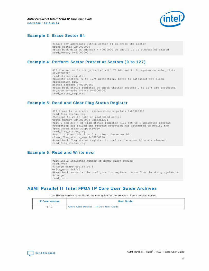
Example 3: Erase Sector 64
#Issue any addresses within sector 64 to erase the sectorerase_sector 0x40000000#read back data at address H'40000000 to ensure it is successful erasedread_memory 0x40000000 1
Example 4: Perform Sector Protect at Sectors (0 to 127)
#If the sector is not protected with TB bit set to 0, system console prints #0x00000000read_status_register#Execute sectors (0 to 127) protection. Refer to datasheet for block #protection bit.sector_protect 0x00000060#read back status register to check whether sectors(0 to 127) are protected, #system console prints 0x00000060read_status_register
Example 5: Read and Clear Flag Status Register
#If there is no errors, system console prints 0x00000080 read_flag_status_reg#Attempt to write data on protected sectorwrite_memory 0x40000000 0xabcd1234#Bit 0 and Bit 4 of flag status register will set to 1 indicates program #operation has failed and program operation has attempted to modify the #protected array respectivelyread_flag_status_reg#set bit 0 and bit 4 to 0 to clear the error bitclear_flag_status_reg 0x00000080#read back flag status register to confirm the error bits are clearedread_flag_status_reg
Example 6: Read and Write nvcr
#Bit 15:12 indicates number of dummy clock cyclesread_nvcr #Change dummy cycles to 8write_nvcr 0x8fff#Read back non-volatile configuration register to confirm the dummy cycles is #changedread_nvcr
ASMI Parallel II Intel FPGA IP Core User Guide ArchivesIf an IP core version is not listed, the user guide for the previous IP core version applies.
IP Core Version User Guide
17.0 Altera ASMI Parallel II IP Core User Guide
ASMI Parallel II Intel® FPGA IP Core User Guide
UG-20068 | 2018.09.24
Send Feedback ASMI Parallel II Intel® FPGA IP Core User Guide
13

Document Revision History for the ASMI Parallel II Intel FPGA IPCore User Guide
Document Version Intel QuartusPrime Version
Changes
2018.09.24 18.0 • Added information on the applications and support for the ASMI ParallelII Intel FPGA IP core.
• Added a note to refer to the Generic Serial Flash Interface Intel FPGAIP Core User Guide.
• Added the ASMI Parallel II Intel FPGA IP Core Use Case Examplessection.
2018.05.07 18.0 • Renamed Altera ASMI Parallel II IP core to ASMI Parallel II Intel FPGAIP core per Intel rebranding.
• Added support for EPCQ-A devices.• Added a note to the clk signal in the Ports Description table.• Updated the description for the qspi_scein signal in the Ports
Description table.• Added a note to the SECTOR_PROTECT register in the Register Map
table.• Updated the bit and width for SECTOR_ERASE and SUBSECTOR_ERASE
registers in the Register Map table.• Updated the bit and width for SECTOR_PROTECT register in the
Register Map table.• Updated the description for the CHIP SELECT option of the CONTROL
register in the Register Map table.• Updated the footnotes for the SECTOR_ERASE, SUBSECTOR_ERASE,
BULK_ERASE, and DIE_ERASE registers in the Register Map table.• Updated the description for the vl_mem_addr signal in the Ports
Description table.• Minor editorial edits.
Date Version Changes
May 2017 2017.05.08 Initial release.
ASMI Parallel II Intel® FPGA IP Core User Guide
UG-20068 | 2018.09.24
ASMI Parallel II Intel® FPGA IP Core User Guide Send Feedback
14