atxmega16a4u-an datasheetww1.microchip.com/downloads/en/devicedoc/atmel-8387-8... ·...
TRANSCRIPT

8/16-bit Atmel XMEGA Microcontroller
ATxmega128A4U / ATxmega64A4U /ATxmega32A4U / ATxmega16A4U
Features
High-performance, low-power Atmel® AVR® XMEGA® 8/16-bit MicrocontrollerNonvolatile program and data memories
16K - 128KB of in-system self-programmable flash4K - 8KB boot section1K - 2KB EEPROM2K - 8KB internal SRAM
Peripheral FeaturesFour-channel DMA controllerEight-channel event systemFive 16-bit timer/counters
Three timer/counters with 4 output compare or input capture channelsTwo timer/counters with 2 output compare or input capture channelsHigh-resolution extensions on all timer/countersAdvanced waveform extension (AWeX) on one timer/counter
One USB device interfaceUSB 2.0 full speed (12Mbps) and low speed (1.5Mbps) device compliant32 Endpoints with full configuration flexibility
Five USARTs with IrDA support for one USARTTwo Two-wire interfaces with dual address match (I2C and SMBus compatible)Two serial peripheral interfaces (SPIs)AES and DES crypto engineCRC-16 (CRC-CCITT) and CRC-32 (IEEE® 802.3) generator16-bit real time counter (RTC) with separate oscillatorOne twelve-channel, 12-bit, 2msps Analog to Digital ConverterOne two-channel, 12-bit, 1msps Digital to Analog ConverterTwo Analog Comparators with window compare function, and current sourcesExternal interrupts on all general purpose I/O pinsProgrammable watchdog timer with separate on-chip ultra low power oscillator QTouch® library support
Capacitive touch buttons, sliders and wheelsSpecial microcontroller features
Power-on reset and programmable brown-out detectionInternal and external clock options with PLL and prescalerProgrammable multilevel interrupt controllerFive sleep modesProgramming and debug interfaces
PDI (program and debug interface)I/O and packages
34 Programmable I/O pins44 - lead TQFP44 - pad VQFN/QFN49 - ball VFBGA
Operating voltage1.6 – 3.6V
Operating frequency0 – 12MHz from 1.6V0 – 32MHz from 2.7V
Atmel-8387H-AVR-ATxmega16A4U-34A4U-64A4U-128A4U-Datasheet_09/2014

1. Ordering InformationOrdering code Flash (bytes) EEPROM (bytes) SRAM (bytes) Speed (MHz) Power supply Package (1)(2)(3) Temp.
ATxmega128A4U-AU 128K + 8K 2K 8K
32 1.6 - 3.6V
44A
-40°C - 85°C
ATxmega128A4U-AUR(4) 128K + 8K 2K 8K
ATxmega64A4U-AU 64K + 4K 2K 4K
ATxmega64A4U-AUR(4) 64K + 4K 2K 4K
ATxmega32A4U-AU 32K + 4K 1K 4K
ATxmega32A4U-AUR(4) 32K + 4K 1K 4K
ATxmega16A4U-AU 16K + 4K 1K 2K
ATxmega16A4U-AUR(4) 16K + 4K 1K 2K
ATxmega128A4U-MH 128K + 8K 2K 8K
PWATxmega128A4U-MHR(4) 128K + 8K 2K 8K
ATxmega64A4U-MH 64K + 4K 2K 4K
ATxmega64A4U-MHR(4) 64K + 4K 2K 4K
ATxmega32A4U-MH 32K + 4K 1K 4K
44M1ATxmega32A4U-MHR(4) 32K + 4K 1K 4K
ATxmega16A4U-MH 16K + 4K 1K 2K
ATxmega16A4U-MHR(4) 16K + 4K 1K 2K
ATxmega128A4U-CU 128K + 8K 2K 8K
49C2
ATxmega128A4U-CUR(4) 128K + 8K 2K 8K
ATxmega64A4U-CU 64K + 4K 2K 4K
ATxmega64A4U-CUR(4) 64K + 4K 2K 4K
ATxmega32A4U-CU 32K + 4K 1K 4K
ATxmega32A4U-CUR(4) 32K + 4K 1K 4K
ATxmega16A4U-CU 16K + 4K 1K 2K
ATxmega16A4U-CUR(4) 16K + 4K 1K 2K
2XMEGA A4U [DATASHEET]Atmel-8387H-AVR-ATxmega16A4U-34A4U-64A4U-128A4U-Datasheet_09/2014

Notes: 1. This device can also be supplied in wafer form. Please contact your local Atmel sales office for detailed ordering information.2. Pb-free packaging, complies to the European Directive for Restriction of Hazardous Substances (RoHS directive). Also Halide free and fully Green.3. For packaging information, see “Instruction Set Summary” on page 63.4. Tape and Reel
Typical Applications
ATxmega128A4U-AN 128K + 8K 2K 8K
32 1.6 - 3.6V
44A
0°C - 105°C
ATxmega128A4U-ANR(4) 128K + 8K 2K 8K
ATxmega64A4U-AN 64K + 4K 2K 4K
ATxmega64A4U-ANR(4) 64K + 4K 2K 4K
ATxmega32A4U-AN 32K + 4K 1K 4K
ATxmega32A4U-ANR(4) 32K + 4K 1K 4K
ATxmega16A4U-AN 16K + 4K 1K 2K
ATxmega16A4U-ANR(4) 16K + 4K 1K 2K
ATxmega128A4U-M7 128K + 8K 2K 8K
PWATxmega128A4U-M7R(4) 128K + 8K 2K 8K
ATxmega64A4U-M7 64K + 4K 2K 4K
ATxmega64A4U-M7R(4) 64K + 4K 2K 4K
ATxmega32A4U-M7 32K + 4K 1K 4K
44M1ATxmega32A4U-M7R(4) 32K + 4K 1K 4K
ATxmega16A4U-M7 16K + 4K 1K 2K
ATxmega16A4U-M7R(4) 16K + 4K 1K 2K
Package Type
44A 44-Lead, 10 x 10mm body size, 1.0mm body thickness, 0.8mm lead pitch, thin profile plastic quad flat package (TQFP)
44M1 44-Pad, 7x7x1mm body, lead pitch 0.50mm, 5.20mm exposed pad, thermally enhanced plastic very thin quad no lead package (VQFN)
PW 44-Pad, 7x7x1mm body, lead pitch 0.50mm, 5.20mm exposed pad, thermally enhanced plastic very thin quad no lead package (VQFN)
49C2 49-Ball (7 x 7 Array), 0.65mm Pitch, 5.0 x 5.0 x 1.0mm, very thin, fine-pitch ball grid array package (VFBGA)
Industrial control Climate control Low power battery applications
Factory automation RF and ZigBee® Power tools
Building control USB connectivity HVAC
Board control Sensor control Utility metering
White goods Optical Medical applications
Ordering code Flash (bytes) EEPROM (bytes) SRAM (bytes) Speed (MHz) Power supply Package (1)(2)(3) Temp.
3XMEGA A4U [DATASHEET]Atmel-8387H-AVR-ATxmega16A4U-34A4U-64A4U-128A4U-Datasheet_09/2014

2. Pinout/Block Diagram
Figure 2-1. Block Diagram and QFN/TQFP pinout
Note: 1. For full details on pinout and pin functions refer to “Pinout and Pin Functions” on page 55.
1
2
3
4
44 43 42 41 40 39 38
5
6
7
8
9
10
11
33
32
31
30
29
28
27
26
25
24
23
37 36 35 34
12 13 14 15 16 17 18 19 20 21 22
PA0
PA1
PA2
PA3
PA4
PB0
PB1
PB3
PB2
PA7
PA6
PA5
GND
VCC
PC0
VCC
GN
D
PC1
PC2
PC3
PC4
PC5
PC6
PC7
PD0
PD1
PD2
PD3
PD4
PD5
PD6
VCC
GND
PD7
PE0
PE1
PE2
PE3
RESE
T/PD
I
PDI
PR0
PR1
AV
CC
GN
DPower
Supervision
Port
A
EVENT ROUTING NETWORK
DMAController
BUSmatrix
SRAMFLASH
ADC
AC0:1
OCD
Port EPort D
Prog/DebugInterface
EEPROM
Port C
TC0:
1
Event System Controller
WatchdogTimer
WatchdogOSC/CLKControl
Real TimeCounter
Interrupt Controller
DATA BUS
DATA BUS
Port RU
SAR
T0:1
TWI
SPI
TC0:
1
USA
RT0
:1
SPI
TC0
USA
RT0
TWI
Port
B
DAC
AREF
AREFSleep
ControllerReset
Controller
IRC
OM
Crypto / CRC
USB
CPUInternalreferences
Internaloscillators
XOSC TOSC
Digital functionAnalog function / Oscillators
Programming, debug, testExternal clock / Crystal pinsGeneral Purpose I /O
GroundPower
4XMEGA A4U [DATASHEET]Atmel-8387H-AVR-ATxmega16A4U-34A4U-64A4U-128A4U-Datasheet_09/2014

Figure 2-2. BGA pinout
Table 2-1. BGA pinout
A
B
C
D
E
F
G
1 2 3 4 5 6 7
A
B
C
D
E
F
G
7 6 5 4 3 2 1Top view Bottom view
1 2 3 4 5 6 7
A PA3 AVCC GND PR1 PR0 PDI_DATA PE3
B PA4 PA1 PA0 GNDRESET/
PDI_CLKPE2 VCC
C PA5 PA2 PA6 PA7 GND PE1 GND
D PB1 PB2 PB3 PB0 GND PD7 PE0
E GND GND PC3 GND PD4 PD5 PD6
F VCC PC0 PC4 PC6 PD0 PD1 PD3
G PC1 PC2 PC5 PC7 GND VCC PD2
5XMEGA A4U [DATASHEET]Atmel-8387H-AVR-ATxmega16A4U-34A4U-64A4U-128A4U-Datasheet_09/2014

3. OverviewThe Atmel AVR XMEGA is a family of low power, high performance, and peripheral rich 8/16-bit microcontrollers based on the AVR enhanced RISC architecture. By executing instructions in a single clock cycle, the AVR XMEGA devices achieve CPU throughput approaching one million instructions per second (MIPS) per megahertz, allowing the system designer to optimize power consumption versus processing speed.
The AVR CPU combines a rich instruction set with 32 general purpose working registers. All 32 registers are directly connected to the arithmetic logic unit (ALU), allowing two independent registers to be accessed in a single instruction, executed in one clock cycle. The resulting architecture is more code efficient while achieving throughputs many times faster than conventional single-accumulator or CISC based microcontrollers.
The AVR XMEGA A4U devices provide the following features: in-system programmable flash with read-while-write capabilities; internal EEPROM and SRAM; four-channel DMA controller, eight-channel event system and programmable multilevel interrupt controller, 34 general purpose I/O lines, 16-bit real-time counter (RTC); five flexible, 16-bit timer/counters with compare and PWM channels; five USARTs; two two-wire serial interfaces (TWIs); one full speed USB 2.0 interface; two serial peripheral interfaces (SPIs); AES and DES cryptographic engine; one twelve-channel, 12-bit ADC with programmable gain; one 2-channel 12-bit DAC; two analog comparators (ACs) with window mode; programmable watchdog timer with separate internal oscillator; accurate internal oscillators with PLL and prescaler; and programmable brown-out detection.
The program and debug interface (PDI), a fast, two-pin interface for programming and debugging, is available.
The ATx devices have five software selectable power saving modes. The idle mode stops the CPU while allowing the SRAM, DMA controller, event system, interrupt controller, and all peripherals to continue functioning. The power-down mode saves the SRAM and register contents, but stops the oscillators, disabling all other functions until the next TWI, USB resume, or pin-change interrupt, or reset. In power-save mode, the asynchronous real-time counter continues to run, allowing the application to maintain a timer base while the rest of the device is sleeping. In standby mode, the external crystal oscillator keeps running while the rest of the device is sleeping. This allows very fast startup from the external crystal, combined with low power consumption. In extended standby mode, both the main oscillator and the asynchronous timer continue to run. To further reduce power consumption, the peripheral clock to each individual peripheral can optionally be stopped in active mode and idle sleep mode.
Atmel offers a free QTouch library for embedding capacitive touch buttons, sliders and wheels functionality into AVR microcontrollers.
The devices are manufactured using Atmel high-density, nonvolatile memory technology. The program flash memory can be reprogrammed in-system through the PDI. A boot loader running in the device can use any interface to download the application program to the flash memory. The boot loader software in the boot flash section will continue to run while the application flash section is updated, providing true read-while-write operation. By combining an 8/16-bit RISC CPU with in-system, self-programmable flash, the AVR XMEGA is a powerful microcontroller family that provides a highly flexible and cost effective solution for many embedded applications.
All Atmel AVR XMEGA devices are supported with a full suite of program and system development tools, including C compilers, macro assemblers, program debugger/simulators, programmers, and evaluation kits.
6XMEGA A4U [DATASHEET]Atmel-8387H-AVR-ATxmega16A4U-34A4U-64A4U-128A4U-Datasheet_09/2014

3.1 Block Diagram
Figure 3-1. XMEGA A4U Block Diagram
Power SupervisionPOR/BOD &
RESET
PORT A (8)
PORT B (8)
DMAController
SRAM
ADCA
ACA
DACB
OCD
Int. Refs.
PDI
PA[0..7]
PB[0..7]
Watchdog Timer
WatchdogOscillator
Interrupt Controller
DATA BUS
Prog/DebugController
VCC
GND
Oscillator Circuits/
ClockGeneration
Oscillator Control
Real TimeCounter
Event System Controller
AREFA
AREFB
PDI_DATA
RESET/PDI_CLK
Sleep Controller
DES
CRC
PORT C (8)
PC[0..7]
TCC
0:1
USA
RTC
0:1
TWIC
SPIC
PD[0..7] PE[0..3]
PORT D (8)
TCD
0:1
USA
RTD
0:1
SPID
TCE0
USA
RTE
0
TWIE
PORT E (4)
TemprefAES
USB
PORT R (2)
DATA BUS
NVM Controller
MORPEEhsalF
IRCOM
BUS Matrix
CPU
EVENT ROUTING NETWORK
XTAL1/TOSC1
XTAL2/TOSC2
PR[0..1]
TOSC1 (optional)
TOSC2(optional)
Digital functionAnalog function
Programming, debug, testOscillator/Crystal/ClockGeneral Purpose I/O
7XMEGA A4U [DATASHEET]Atmel-8387H-AVR-ATxmega16A4U-34A4U-64A4U-128A4U-Datasheet_09/2014

4. ResourcesA comprehensive set of development tools, application notes and datasheets are available for download on http://www.atmel.com/avr.
4.1 Recommended readingAtmel AVR XMEGA AU manualXMEGA application notes
This device data sheet only contains part specific information with a short description of each peripheral and module. The XMEGA AU manual describes the modules and peripherals in depth. The XMEGA application notes contain example code and show applied use of the modules and peripherals.
All documentation are available from www.atmel.com/avr.
5. Capacitive touch sensingThe Atmel QTouch library provides a simple to use solution to realize touch sensitive interfaces on most Atmel AVR microcontrollers. The patented charge-transfer signal acquisition offers robust sensing and includes fully debounced reporting of touch keys and includes Adjacent Key Suppression® (AKS®) technology for unambiguous detection of key events. The QTouch library includes support for the QTouch and QMatrix acquisition methods.
Touch sensing can be added to any application by linking the appropriate Atmel QTouch library for the AVR microcontroller. This is done by using a simple set of APIs to define the touch channels and sensors, and then calling the touch sensing API’s to retrieve the channel information and determine the touch sensor states.
The QTouch library is FREE and downloadable from the Atmel website at the following location: www.atmel.com/qtouchlibrary. For implementation details and other information, refer to the QTouch library user guide - also available for download from the Atmel website.
8XMEGA A4U [DATASHEET]Atmel-8387H-AVR-ATxmega16A4U-34A4U-64A4U-128A4U-Datasheet_09/2014
6. AVR CPU
6.1 Features8/16-bit, high-performance Atmel AVR RISC CPU
142 instructionsHardware multiplier
32x8-bit registers directly connected to the ALUStack in RAMStack pointer accessible in I/O memory spaceDirect addressing of up to 16MB of program memory and 16MB of data memoryTrue 16/24-bit access to 16/24-bit I/O registersEfficient support for 8-, 16-, and 32-bit arithmeticConfiguration change protection of system-critical features
6.2 OverviewAll Atmel AVR XMEGA devices use the 8/16-bit AVR CPU. The main function of the CPU is to execute the code and perform all calculations. The CPU is able to access memories, perform calculations, control peripherals, and execute the program in the flash memory. Interrupt handling is described in a separate section, refer to “Interrupts and Programmable Multilevel Interrupt Controller” on page 29.
6.3 Architectural OverviewIn order to maximize performance and parallelism, the AVR CPU uses a Harvard architecture with separate memories and buses for program and data. Instructions in the program memory are executed with single-level pipelining. While one instruction is being executed, the next instruction is pre-fetched from the program memory. This enables instructions to be executed on every clock cycle. For details of all AVR instructions, refer to http://www.atmel.com/avr.
9XMEGA A4U [DATASHEET]Atmel-8387H-AVR-ATxmega16A4U-34A4U-64A4U-128A4U-Datasheet_09/2014

Figure 6-1. Block diagram of the AVR CPU architecture.
The arithmetic logic unit (ALU) supports arithmetic and logic operations between registers or between a constant and a register. Single-register operations can also be executed in the ALU. After an arithmetic operation, the status register is updated to reflect information about the result of the operation.
The ALU is directly connected to the fast-access register file. The 32 x 8-bit general purpose working registers all have single clock cycle access time allowing single-cycle arithmetic logic unit (ALU) operation between registers or between a register and an immediate. Six of the 32 registers can be used as three 16-bit address pointers for program and data space addressing, enabling efficient address calculations.
The memory spaces are linear. The data memory space and the program memory space are two different memory spaces.
The data memory space is divided into I/O registers, SRAM, and external RAM. In addition, the EEPROM can be memory mapped in the data memory.
All I/O status and control registers reside in the lowest 4KB addresses of the data memory. This is referred to as the I/O memory space. The lowest 64 addresses can be accessed directly, or as the data space locations from 0x00 to 0x3F. The rest is the extended I/O memory space, ranging from 0x0040 to 0x0FFF. I/O registers here must be accessed as data space locations using load (LD/LDS/LDD) and store (ST/STS/STD) instructions.
The SRAM holds data. Code execution from SRAM is not supported. It can easily be accessed through the five different addressing modes supported in the AVR architecture. The first SRAM address is 0x2000.
Data addresses 0x1000 to 0x1FFF are reserved for memory mapping of EEPROM.
The program memory is divided in two sections, the application program section and the boot program section. Both sections have dedicated lock bits for write and read/write protection. The SPM instruction that is used for self-programming of the application flash memory must reside in the boot program section. The application section contains an application table section with separate lock bits for write and read/write protection. The application table section can be used for safe storing of nonvolatile data in the program memory.
6.4 ALU - Arithmetic Logic UnitThe arithmetic logic unit (ALU) supports arithmetic and logic operations between registers or between a constant and a register. Single-register operations can also be executed. The ALU operates in direct connection with all 32 general
10XMEGA A4U [DATASHEET]Atmel-8387H-AVR-ATxmega16A4U-34A4U-64A4U-128A4U-Datasheet_09/2014

purpose registers. In a single clock cycle, arithmetic operations between general purpose registers or between a register and an immediate are executed and the result is stored in the register file. After an arithmetic or logic operation, the status register is updated to reflect information about the result of the operation.
ALU operations are divided into three main categories – arithmetic, logical, and bit functions. Both 8- and 16-bit arithmetic is supported, and the instruction set allows for efficient implementation of 32-bit aritmetic. The hardware multiplier supports signed and unsigned multiplication and fractional format.
6.4.1 Hardware Multiplier
The multiplier is capable of multiplying two 8-bit numbers into a 16-bit result. The hardware multiplier supports different variations of signed and unsigned integer and fractional numbers:
Multiplication of unsigned integersMultiplication of signed integersMultiplication of a signed integer with an unsigned integerMultiplication of unsigned fractional numbersMultiplication of signed fractional numbersMultiplication of a signed fractional number with an unsigned one
A multiplication takes two CPU clock cycles.
6.5 Program FlowAfter reset, the CPU starts to execute instructions from the lowest address in the flash programmemory ‘0.’ The program counter (PC) addresses the next instruction to be fetched.
Program flow is provided by conditional and unconditional jump and call instructions capable of addressing the whole address space directly. Most AVR instructions use a 16-bit word format, while a limited number use a 32-bit format.
During interrupts and subroutine calls, the return address PC is stored on the stack. The stack is allocated in the general data SRAM, and consequently the stack size is only limited by the total SRAM size and the usage of the SRAM. After reset, the stack pointer (SP) points to the highest address in the internal SRAM. The SP is read/write accessible in the I/O memory space, enabling easy implementation of multiple stacks or stack areas. The data SRAM can easily be accessed through the five different addressing modes supported in the AVR CPU.
6.6 Status RegisterThe status register (SREG) contains information about the result of the most recently executed arithmetic or logic instruction. This information can be used for altering program flow in order to perform conditional operations. Note that the status register is updated after all ALU operations, as specified in the instruction set reference. This will in many cases remove the need for using the dedicated compare instructions, resulting in faster and more compact code.
The status register is not automatically stored when entering an interrupt routine nor restored when returning from an interrupt. This must be handled by software.
The status register is accessible in the I/O memory space.
6.7 Stack and Stack PointerThe stack is used for storing return addresses after interrupts and subroutine calls. It can also be used for storing temporary data. The stack pointer (SP) register always points to the top of the stack. It is implemented as two 8-bit registers that are accessible in the I/O memory space. Data are pushed and popped from the stack using the PUSH and POP instructions. The stack grows from a higher memory location to a lower memory location. This implies that pushing data onto the stack decreases the SP, and popping data off the stack increases the SP. The SP is automatically loaded after reset, and the initial value is the highest address of the internal SRAM. If the SP is changed, it must be set to point above address 0x2000, and it must be defined before any subroutine calls are executed or before interrupts are enabled.
11XMEGA A4U [DATASHEET]Atmel-8387H-AVR-ATxmega16A4U-34A4U-64A4U-128A4U-Datasheet_09/2014

During interrupts or subroutine calls, the return address is automatically pushed on the stack. The return address can be two or three bytes, depending on program memory size of the device. For devices with 128KB or less of program memory, the return address is two bytes, and hence the stack pointer is decremented/incremented by two. For devices with more than 128KB of program memory, the return address is three bytes, and hence the SP is decremented/incremented by three. The return address is popped off the stack when returning from interrupts using the RETI instruction, and from subroutine calls using the RET instruction.
The SP is decremented by one when data are pushed on the stack with the PUSH instruction, and incremented by one when data is popped off the stack using the POP instruction.
To prevent corruption when updating the stack pointer from software, a write to SPL will automatically disable interrupts for up to four instructions or until the next I/O memory write.
After reset the stack pointer is initialized to the highest address of the SRAM. See Figure 7-1 on page 16.
6.8 Register FileThe register file consists of 32 x 8-bit general purpose working registers with single clock cycle access time. The register file supports the following input/output schemes:
One 8-bit output operand and one 8-bit result inputTwo 8-bit output operands and one 8-bit result inputTwo 8-bit output operands and one 16-bit result inputOne 16-bit output operand and one 16-bit result input
Six of the 32 registers can be used as three 16-bit address register pointers for data space addressing, enabling efficient address calculations. One of these address pointers can also be used as an address pointer for lookup tables in flash program memory.
12XMEGA A4U [DATASHEET]Atmel-8387H-AVR-ATxmega16A4U-34A4U-64A4U-128A4U-Datasheet_09/2014

7. Memories
7.1 FeaturesFlash program memory
One linear address spaceIn-system programmableSelf-programming and boot loader supportApplication section for application codeApplication table section for application code or data storageBoot section for application code or boot loader codeSeparate read/write protection lock bits for all sectionsBuilt in fast CRC check of a selectable flash program memory section
Data memoryOne linear address spaceSingle-cycle access from CPUSRAMEEPROM
Byte and page accessibleOptional memory mapping for direct load and store
I/O memoryConfiguration and status registers for all peripherals and modules16 bit-accessible general purpose registers for global variables or flags
Bus arbitrationDeterministic priority handling between CPU, DMA controller, and other bus masters
Separate buses for SRAM, EEPROM and I/O memorySimultaneous bus access for CPU and DMA controller
Production signature row memory for factory programmed dataID for each microcontroller device typeSerial number for each deviceCalibration bytes for factory calibrated peripherals
User signature rowOne flash page in sizeCan be read and written from softwareContent is kept after chip erase
7.2 OverviewThe Atmel AVR architecture has two main memory spaces, the program memory and the data memory. Executable code can reside only in the program memory, while data can be stored in the program memory and the data memory. The data memory includes the internal SRAM, and EEPROM for nonvolatile data storage. All memory spaces are linear and require no memory bank switching. Nonvolatile memory (NVM) spaces can be locked for further write and read/write operations. This prevents unrestricted access to the application software.
A separate memory section contains the fuse bytes. These are used for configuring important system functions, and can only be written by an external programmer.
The available memory size configurations are shown in “Ordering Information” on page 2. In addition, each device has a Flash memory signature row for calibration data, device identification, serial number etc.
13XMEGA A4U [DATASHEET]Atmel-8387H-AVR-ATxmega16A4U-34A4U-64A4U-128A4U-Datasheet_09/2014

7.3 Flash Program MemoryThe Atmel AVR XMEGA devices contain on-chip, in-system reprogrammable flash memory for program storage. The flash memory can be accessed for read and write from an external programmer through the PDI or from application software running in the device.
All AVR CPU instructions are 16 or 32 bits wide, and each flash location is 16 bits wide. The flash memory is organized in two main sections, the application section and the boot loader section. The sizes of the different sections are fixed, but device-dependent. These two sections have separate lock bits, and can have different levels of protection. The store program memory (SPM) instruction, which is used to write to the flash from the application software, will only operate when executed from the boot loader section.
The application section contains an application table section with separate lock settings. This enables safe storage of nonvolatile data in the program memory.
Table 7-1. Flash Program Memory (Hexadecimal address).
7.3.1 Application Section
The Application section is the section of the flash that is used for storing the executable application code. The protection level for the application section can be selected by the boot lock bits for this section. The application section can not store any boot loader code since the SPM instruction cannot be executed from the application section.
7.3.2 Application Table Section
The application table section is a part of the application section of the flash memory that can be used for storing data. The size is identical to the boot loader section. The protection level for the application table section can be selected by the boot lock bits for this section. The possibilities for different protection levels on the application section and the application table section enable safe parameter storage in the program memory. If this section is not used for data, application code can reside here.
7.3.3 Boot Loader Section
While the application section is used for storing the application code, the boot loader software must be located in the boot loader section because the SPM instruction can only initiate programming when executing from this section. The SPM instruction can access the entire flash, including the boot loader section itself. The protection level for the boot loader section can be selected by the boot loader lock bits. If this section is not used for boot loader software, application code can be stored here.
Word Address
ATxmega128A4U ATxmega64A4U ATxmega32A4U ATxmega16A4U
0 0 0 0 Application Section (128K/64K/32K/16K)
...
EFFF / 77FF / 37FF / 17FF
F000 / 7800 / 3800 / 1800 Application Table Section (8K/4K/4K/4K)FFFF / 7FFF / 3FFF / 1FFF
10000 / 8000 / 4000 / 2000 Boot Section (8K/4K/4K/4K)10FFF / 87FF / 47FF / 27FF
14XMEGA A4U [DATASHEET]Atmel-8387H-AVR-ATxmega16A4U-34A4U-64A4U-128A4U-Datasheet_09/2014

7.3.4 Production Signature Row
The production signature row is a separate memory section for factory programmed data. It contains calibration data for functions such as oscillators and analog modules. Some of the calibration values will be automatically loaded to the corresponding module or peripheral unit during reset. Other values must be loaded from the signature row and written to the corresponding peripheral registers from software. For details on calibration conditions, refer to “Electrical Characteristics” on page 72.
The production signature row also contains an ID that identifies each microcontroller device type and a serial number for each manufactured device. The serial number consists of the production lot number, wafer number, and wafer coordinates for the device. The device ID for the available devices is shown in Table 7-2.
The production signature row cannot be written or erased, but it can be read from application software and external programmers.
Table 7-2. Device ID bytes for Atmel AVR XMEGA A4U devices.
7.3.5 User Signature Row
The user signature row is a separate memory section that is fully accessible (read and write) from application software and external programmers. It is one flash page in size, and is meant for static user parameter storage, such as calibration data, custom serial number, identification numbers, random number seeds, etc. This section is not erased by chip erase commands that erase the flash, and requires a dedicated erase command. This ensures parameter storage during multiple program/erase operations and on-chip debug sessions.
7.4 Fuses and Lock bitsThe fuses are used to configure important system functions, and can only be written from an external programmer. The application software can read the fuses. The fuses are used to configure reset sources such as brownout detector and watchdog, and startup configuration.
The lock bits are used to set protection levels for the different flash sections (that is, if read and/or write access should be blocked). Lock bits can be written by external programmers and application software, but only to stricter protection levels. Chip erase is the only way to erase the lock bits. To ensure that flash contents are protected even during chip erase, the lock bits are erased after the rest of the flash memory has been erased.
An unprogrammed fuse or lock bit will have the value one, while a programmed fuse or lock bit will have the value zero.
Both fuses and lock bits are reprogrammable like the flash program memory.
7.5 Data MemoryThe data memory contains the I/O memory, internal SRAM, optionally memory mapped EEPROM, and external memory if available. The data memory is organized as one continuous memory section, see Figure 7-1. To simplify development, I/O Memory, EEPROM and SRAM will always have the same start addresses for all Atmel AVR XMEGA devices.
Device Device ID bytes
Byte 2 Byte 1 Byte 0
ATxmega16A4U 41 94 1E
ATxmega32A4U 41 95 1E
ATxmega64A4U 46 96 1E
ATxmega128A4U 46 97 1E
15XMEGA A4U [DATASHEET]Atmel-8387H-AVR-ATxmega16A4U-34A4U-64A4U-128A4U-Datasheet_09/2014

Figure 7-1. Data memory map (Hexadecimal address).
7.6 EEPROMAll devices have EEPROM for nonvolatile data storage. It is either addressable in a separate data space (default) or memory mapped and accessed in normal data space. The EEPROM supports both byte and page access. Memory mapped EEPROM allows highly efficient EEPROM reading and EEPROM buffer loading. When doing this, EEPROM is accessible using load and store instructions. Memory mapped EEPROM will always start at hexadecimal address 0x1000.
7.7 I/O MemoryThe status and configuration registers for peripherals and modules, including the CPU, are addressable through I/O memory locations. All I/O locations can be accessed by the load (LD/LDS/LDD) and store (ST/STS/STD) instructions, which are used to transfer data between the 32 registers in the register file and the I/O memory. The IN and OUT instructions can address I/O memory locations in the range of 0x00 to 0x3F directly. In the address range 0x00 - 0x1F, single-cycle instructions for manipulation and checking of individual bits are available.
The I/O memory address for all peripherals and modules in XMEGA A4U is shown in the “Peripheral Module Address Map” on page 61.
7.7.1 General Purpose I/O Registers
The lowest 16 I/O memory addresses are reserved as general purpose I/O registers. These registers can be used for storing global variables and flags, as they are directly bit-accessible using the SBI, CBI, SBIS, and SBIC instructions.
Byte Address ATxmega64A4U Byte Address ATxmega32A4U Byte Address ATxmega16A4U
0I/O Registers (4K)
0I/O Registers (4K)
0I/O Registers (4K)
FFF FFF FFF
1000EEPROM (2K)
1000EEPROM (1K)
1000EEPROM (1K)
17FF 13FF 13FF
RESERVED RESERVED RESERVED
2000Internal SRAM (4K)
2000Internal SRAM (4K)
2000Internal SRAM (2K)
2FFF 2FFF 27FF
Byte Address ATxmega128A4U
0I/O Registers (4K)
FFF
1000EEPROM (2K)
17FF
RESERVED
2000Internal SRAM (8K)
3FFF
16XMEGA A4U [DATASHEET]Atmel-8387H-AVR-ATxmega16A4U-34A4U-64A4U-128A4U-Datasheet_09/2014

7.8 Data Memory and Bus ArbitrationSince the data memory is organized as four separate sets of memories, the different bus masters (CPU, DMA controller read and DMA controller write, etc.) can access different memory sections at the same time.
7.9 Memory TimingRead and write access to the I/O memory takes one CPU clock cycle. A write to SRAM takes one cycle, and a read from SRAM takes two cycles. For burst read (DMA), new data are available every cycle. EEPROM page load (write) takes one cycle, and three cycles are required for read. For burst read, new data are available every second cycle. Refer to the instruction summary for more details on instructions and instruction timing.
7.10 Device ID and RevisionEach device has a three-byte device ID. This ID identifies Atmel as the manufacturer of the device and the device type. A separate register contains the revision number of the device.
7.11 I/O Memory ProtectionSome features in the device are regarded as critical for safety in some applications. Due to this, it is possible to lock the I/O register related to the clock system, the event system, and the advanced waveform extensions. As long as the lock is enabled, all related I/O registers are locked and they can not be written from the application software. The lock registers themselves are protected by the configuration change protection mechanism.
7.12 Flash and EEPROM Page SizeThe flash program memory and EEPROM data memory are organized in pages. The pages are word accessible for the flash and byte accessible for the EEPROM.
Table 7-3 on page 17 shows the Flash Program Memory organization and Program Counter (PC) size. Flash write and erase operations are performed on one page at a time, while reading the Flash is done one byte at a time. For Flash access the Z-pointer (Z[m:n]) is used for addressing. The most significant bits in the address (FPAGE) give the page number and the least significant address bits (FWORD) give the word in the page.
Table 7-3. Number of words and pages in the flash.
Table 7-4 shows EEPROM memory organization for the Atmel AVR XMEGA A4U devices. EEEPROM write and erase operations can be performed one page or one byte at a time, while reading the EEPROM is done one byte at a time. For EEPROM access the NVM address register (ADDR[m:n]) is used for addressing. The most significant bits in the address (E2PAGE) give the page number and the least significant address bits (E2BYTE) give the byte in the page.
Devices PC size Flash size Page Size FWORD FPAGE Application Boot
bits bytes words Size No of pages Size No of
pages
ATxmega16A4U 14 16K + 4K 128 Z[6:0] Z[13:7] 16K 64 4K 16
ATxmega32A4U 15 32K + 4K 128 Z[6:0] Z[14:7] 32K 128 4K 16
ATxmega64A4U 16 64K + 4K 128 Z[6:0] Z[15:7] 64K 256 4K 16
ATxmega128A4U 17 128K + 8K 128 Z[6:0] Z[16:7] 128K 512 8K 32
17XMEGA A4U [DATASHEET]Atmel-8387H-AVR-ATxmega16A4U-34A4U-64A4U-128A4U-Datasheet_09/2014

Table 7-4. Number of bytes and pages in the EEPROM.
Devices EEPROM Page Size E2BYTE E2PAGE No of Pages
Size bytes
ATxmega16A4U 1K 32 ADDR[4:0] ADDR[10:5] 32
ATxmega32A4U 1K 32 ADDR[4:0] ADDR[10:5] 32
ATxmega64A4U 2K 32 ADDR[4:0] ADDR[10:5] 64
ATxmega128A4U 2K 32 ADDR[4:0] ADDR[10:5] 64
18XMEGA A4U [DATASHEET]Atmel-8387H-AVR-ATxmega16A4U-34A4U-64A4U-128A4U-Datasheet_09/2014

8. DMAC – Direct Memory Access Controller
8.1 FeaturesAllows high speed data transfers with minimal CPU intervention
from data memory to data memoryfrom data memory to peripheralfrom peripheral to data memoryfrom peripheral to peripheral
Four DMA channels with separatetransfer triggersinterrupt vectorsaddressing modes
Programmable channel priorityFrom 1 byte to 16MB of data in a single transaction
Up to 64KB block transfers with repeat1, 2, 4, or 8 byte burst transfers
Multiple addressing modesStaticIncrementalDecremental
Optional reload of source and destination addresses at the end of eachBurstBlockTransaction
Optional interrupt on end of transactionOptional connection to CRC generator for CRC on DMA data
8.2 OverviewThe four-channel direct memory access (DMA) controller can transfer data between memories and peripherals, and thus offload these tasks from the CPU. It enables high data transfer rates with minimum CPU intervention, and frees up CPU time. The four DMA channels enable up to four independent and parallel transfers.
The DMA controller can move data between SRAM and peripherals, between SRAM locations and directly between peripheral registers. With access to all peripherals, the DMA controller can handle automatic transfer of data to/from communication modules. The DMA controller can also read from memory mapped EEPROM.
Data transfers are done in continuous bursts of 1, 2, 4, or 8 bytes. They build block transfers of configurable size from 1 byte to 64KB. A repeat counter can be used to repeat each block transfer for single transactions up to 16MB. Source and destination addressing can be static, incremental or decremental. Automatic reload of source and/or destination addresses can be done after each burst or block transfer, or when a transaction is complete. Application software, peripherals, and events can trigger DMA transfers.
The four DMA channels have individual configuration and control settings. This include source, destination, transfer triggers, and transaction sizes. They have individual interrupt settings. Interrupt requests can be generated when a transaction is complete or when the DMA controller detects an error on a DMA channel.
To allow for continuous transfers, two channels can be interlinked so that the second takes over the transfer when the first is finished, and vice versa.
19XMEGA A4U [DATASHEET]Atmel-8387H-AVR-ATxmega16A4U-34A4U-64A4U-128A4U-Datasheet_09/2014

9. Event System
9.1 FeaturesSystem for direct peripheral-to-peripheral communication and signalingPeripherals can directly send, receive, and react to peripheral events
CPU and DMA controller independent operation100% predictable signal timingShort and guaranteed response time
Eight event channels for up to eight different and parallel signal routing configurationsEvents can be sent and/or used by most peripherals, clock system, and softwareAdditional functions include
Quadrature decodersDigital filtering of I/O pin state
Works in active mode and idle sleep mode
9.2 OverviewThe event system enables direct peripheral-to-peripheral communication and signaling. It allows a change in one peripheral’s state to automatically trigger actions in other peripherals. It is designed to provide a predictable system for short and predictable response times between peripherals. It allows for autonomous peripheral control and interaction without the use of interrupts, CPU, or DMA controller resources, and is thus a powerful tool for reducing the complexity, size and execution time of application code. It also allows for synchronized timing of actions in several peripheral modules.
A change in a peripheral’s state is referred to as an event, and usually corresponds to the peripheral’s interrupt conditions. Events can be directly passed to other peripherals using a dedicated routing network called the event routing network. How events are routed and used by the peripherals is configured in software.
Figure 9-1 on page 20 shows a basic diagram of all connected peripherals. The event system can directly connect together analog and digital converters, analog comparators, I/O port pins, the real-time counter, timer/counters, IR communication module (IRCOM), and USB interface. It can also be used to trigger DMA transactions (DMA controller). Events can also be generated from software and the peripheral clock.
Figure 9-1. Event system overview and connected peripherals.
The event routing network consists of eight software-configurable multiplexers that control how events are routed and used. These are called event channels, and allow for up to eight parallel event routing configurations. The maximum routing latency is two peripheral clock cycles. The event system works in both active mode and idle sleep mode.
DAC
Timer / Counters
USB
ADCReal Time Counter
Port pins
CPU / Software
DMAController
IRCOM
Event Routing Network
EventSystem
Controller
clkPERPrescaler
AC
20XMEGA A4U [DATASHEET]Atmel-8387H-AVR-ATxmega16A4U-34A4U-64A4U-128A4U-Datasheet_09/2014

10. System Clock and Clock options
10.1 FeaturesFast start-up timeSafe run-time clock switchingInternal oscillators:
32MHz run-time calibrated and tuneable oscillator2MHz run-time calibrated oscillator32.768kHz calibrated oscillator32kHz ultra low power (ULP) oscillator with 1kHz output
External clock options0.4MHz - 16MHz crystal oscillator32.768kHz crystal oscillatorExternal clock
PLL with 20MHz - 128MHz output frequencyInternal and external clock options and 1x to 31x multiplicationLock detector
Clock prescalers with 1x to 2048x divisionFast peripheral clocks running at two and four times the CPU clockAutomatic run-time calibration of internal oscillatorsExternal oscillator and PLL lock failure detection with optional non-maskable interrupt
10.2 OverviewAtmel AVR XMEGA A4U devices have a flexible clock system supporting a large number of clock sources. It incorporates both accurate internal oscillators and external crystal oscillator and resonator support. A high-frequency phase locked loop (PLL) and clock prescalers can be used to generate a wide range of clock frequencies. A calibration feature (DFLL) is available, and can be used for automatic run-time calibration of the internal oscillators to remove frequency drift over voltage and temperature. An oscillator failure monitor can be enabled to issue a non-maskable interrupt and switch to the internal oscillator if the external oscillator or PLL fails.
When a reset occurs, all clock sources except the 32kHz ultra low power oscillator are disabled. After reset, the device will always start up running from the 2MHz internal oscillator. During normal operation, the system clock source and prescalers can be changed from software at any time.
Figure 10-1 on page 22 presents the principal clock system in the XMEGA A4U family of devices. Not all of the clocks need to be active at a given time. The clocks for the CPU and peripherals can be stopped using sleep modes and power reduction registers, as described in “Power Management and Sleep Modes” on page 24.
21XMEGA A4U [DATASHEET]Atmel-8387H-AVR-ATxmega16A4U-34A4U-64A4U-128A4U-Datasheet_09/2014

Figure 10-1. The clock system, clock sources and clock distribution.
10.3 Clock SourcesThe clock sources are divided in two main groups: internal oscillators and external clock sources. Most of the clock sources can be directly enabled and disabled from software, while others are automatically enabled or disabled, depending on peripheral settings. After reset, the device starts up running from the 2MHz internal oscillator. The other clock sources, DFLLs and PLL, are turned off by default.
The internal oscillators do not require any external components to run. For details on characteristics and accuracy of the internal oscillators, refer to the device datasheet.
10.3.1 32kHz Ultra Low Power Internal Oscillator
This oscillator provides an approximate 32kHz clock. The 32kHz ultra low power (ULP) internal oscillator is a very low power clock source, and it is not designed for high accuracy. The oscillator employs a built-in prescaler that provides
Real TimeCounter Peripherals RAM AVR CPU Non-Volatile
Memory
WatchdogTimer
Brown-outDetector
System Clock Prescalers
USB
Prescaler
System Clock Multiplexer(SCLKSEL)
PLLSRC
RTCSRC
DIV32
32 kHzInt. ULP
32.768 kHzInt. OSC
32.768 kHzTOSC
2 MHzInt. Osc
32 MHzInt. Osc
0.4 – 16 MHzXTAL
DIV32
DIV32
DIV4XOSCSEL
PLL
USBSRC
TOSC
1
TOSC
2
XTAL1
XTAL2
clkSYSclkRTC
clkPER2
clkPER
clkCPU
clkPER4
clkUSB
22XMEGA A4U [DATASHEET]Atmel-8387H-AVR-ATxmega16A4U-34A4U-64A4U-128A4U-Datasheet_09/2014

a 1kHz output. The oscillator is automatically enabled/disabled when it is used as clock source for any part of the device. This oscillator can be selected as the clock source for the RTC.
10.3.2 32.768kHz Calibrated Internal Oscillator
This oscillator provides an approximate 32.768kHz clock. It is calibrated during production to provide a default frequency close to its nominal frequency. The calibration register can also be written from software for run-time calibration of the oscillator frequency. The oscillator employs a built-in prescaler, which provides both a 32.768kHz output and a 1.024kHz output.
10.3.3 32.768kHz Crystal Oscillator
A 32.768kHz crystal oscillator can be connected between the TOSC1 and TOSC2 pins and enables a dedicated low frequency oscillator input circuit. A low power mode with reduced voltage swing on TOSC2 is available. This oscillator can be used as a clock source for the system clock and RTC, and as the DFLL reference clock.
10.3.4 0.4 - 16MHz Crystal Oscillator
This oscillator can operate in four different modes optimized for different frequency ranges, all within 0.4 - 16MHz.
10.3.5 2MHz Run-time Calibrated Internal Oscillator
The 2MHz run-time calibrated internal oscillator is the default system clock source after reset. It is calibrated during production to provide a default frequency close to its nominal frequency. A DFLL can be enabled for automatic run-time calibration of the oscillator to compensate for temperature and voltage drift and optimize the oscillator accuracy.
10.3.6 32MHz Run-time Calibrated Internal Oscillator
The 32MHz run-time calibrated internal oscillator is a high-frequency oscillator. It is calibrated during production to provide a default frequency close to its nominal frequency. A digital frequency looked loop (DFLL) can be enabled for automatic run-time calibration of the oscillator to compensate for temperature and voltage drift and optimize the oscillator accuracy. This oscillator can also be adjusted and calibrated to any frequency between 30MHz and 55MHz. The production signature row contains 48MHz calibration values intended used when the oscillator is used a full-speed USB clock source.
10.3.7 External Clock Sources
The XTAL1 and XTAL2 pins can be used to drive an external oscillator, either a quartz crystal or a ceramic resonator. XTAL1 can be used as input for an external clock signal. The TOSC1 and TOSC2 pins is dedicated to driving a 32.768kHz crystal oscillator.
10.3.8 PLL with 1x-31x Multiplication Factor
The built-in phase locked loop (PLL) can be used to generate a high-frequency system clock. The PLL has a user-selectable multiplication factor of from 1 to 31. In combination with the prescalers, this gives a wide range of output frequencies from all clock sources.
23XMEGA A4U [DATASHEET]Atmel-8387H-AVR-ATxmega16A4U-34A4U-64A4U-128A4U-Datasheet_09/2014

11. Power Management and Sleep Modes
11.1 FeaturesPower management for adjusting power consumption and functionsFive sleep modes
IdlePower downPower saveStandbyExtended standby
Power reduction register to disable clock and turn off unused peripherals in active and idle modes
11.2 OverviewVarious sleep modes and clock gating are provided in order to tailor power consumption to application requirements. This enables the Atmel AVR XMEGA microcontroller to stop unused modules to save power.
All sleep modes are available and can be entered from active mode. In active mode, the CPU is executing application code. When the device enters sleep mode, program execution is stopped and interrupts or a reset is used to wake the device again. The application code decides which sleep mode to enter and when. Interrupts from enabled peripherals and all enabled reset sources can restore the microcontroller from sleep to active mode.
In addition, power reduction registers provide a method to stop the clock to individual peripherals from software. When this is done, the current state of the peripheral is frozen, and there is no power consumption from that peripheral. This reduces the power consumption in active mode and idle sleep modes and enables much more fine-tuned power management than sleep modes alone.
11.3 Sleep ModesSleep modes are used to shut down modules and clock domains in the microcontroller in order to save power. XMEGA microcontrollers have five different sleep modes tuned to match the typical functional stages during application execution. A dedicated sleep instruction (SLEEP) is available to enter sleep mode. Interrupts are used to wake the device from sleep, and the available interrupt wake-up sources are dependent on the configured sleep mode. When an enabled interrupt occurs, the device will wake up and execute the interrupt service routine before continuing normal program execution from the first instruction after the SLEEP instruction. If other, higher priority interrupts are pending when the wake-up occurs, their interrupt service routines will be executed according to their priority before the interrupt service routine for the wake-up interrupt is executed. After wake-up, the CPU is halted for four cycles before execution starts.
The content of the register file, SRAM and registers are kept during sleep. If a reset occurs during sleep, the device will reset, start up, and execute from the reset vector.
11.3.1 Idle Mode
In idle mode the CPU and nonvolatile memory are stopped (note that any ongoing programming will be completed), but all peripherals, including the interrupt controller, event system and DMA controller are kept running. Any enabled interrupt will wake the device.
11.3.2 Power-down Mode
In power-down mode, all clocks, including the real-time counter clock source, are stopped. This allows operation only of asynchronous modules that do not require a running clock. The only interrupts that can wake up the MCU are the two-wire interface address match interrupt, asynchronous port interrupts, and the USB resume interrupt.
24XMEGA A4U [DATASHEET]Atmel-8387H-AVR-ATxmega16A4U-34A4U-64A4U-128A4U-Datasheet_09/2014

11.3.3 Power-save Mode
Power-save mode is identical to power down, with one exception. If the real-time counter (RTC) is enabled, it will keep running during sleep, and the device can also wake up from either an RTC overflow or compare match interrupt.
11.3.4 Standby Mode
Standby mode is identical to power down, with the exception that the enabled system clock sources are kept running while the CPU, peripheral, and RTC clocks are stopped. This reduces the wake-up time.
11.3.5 Extended Standby Mode
Extended standby mode is identical to power-save mode, with the exception that the enabled system clock sources are kept running while the CPU and peripheral clocks are stopped. This reduces the wake-up time.
25XMEGA A4U [DATASHEET]Atmel-8387H-AVR-ATxmega16A4U-34A4U-64A4U-128A4U-Datasheet_09/2014

12. System Control and Reset
12.1 FeaturesReset the microcontroller and set it to initial state when a reset source goes activeMultiple reset sources that cover different situations
Power-on resetExternal resetWatchdog resetBrownout resetPDI resetSoftware reset
Asynchronous operationNo running system clock in the device is required for reset
Reset status register for reading the reset source from the application code
12.2 OverviewThe reset system issues a microcontroller reset and sets the device to its initial state. This is for situations where operation should not start or continue, such as when the microcontroller operates below its power supply rating. If a reset source goes active, the device enters and is kept in reset until all reset sources have released their reset. The I/O pins are immediately tri-stated. The program counter is set to the reset vector location, and all I/O registers are set to their initial values. The SRAM content is kept. However, if the device accesses the SRAM when a reset occurs, the content of the accessed location can not be guaranteed.
After reset is released from all reset sources, the default oscillator is started and calibrated before the device starts running from the reset vector address. By default, this is the lowest program memory address, 0, but it is possible to move the reset vector to the lowest address in the boot section.
The reset functionality is asynchronous, and so no running system clock is required to reset the device. The software reset feature makes it possible to issue a controlled system reset from the user software.
The reset status register has individual status flags for each reset source. It is cleared at power-on reset, and shows which sources have issued a reset since the last power-on.
12.3 Reset SequenceA reset request from any reset source will immediately reset the device and keep it in reset as long as the request is active. When all reset requests are released, the device will go through three stages before the device starts running again:
Reset counter delayOscillator startupOscillator calibration
If another reset requests occurs during this process, the reset sequence will start over again.
12.4 Reset Sources
12.4.1 Power-on Reset
A power-on reset (POR) is generated by an on-chip detection circuit. The POR is activated when the VCC rises and reaches the POR threshold voltage (VPOT), and this will start the reset sequence.
The POR is also activated to power down the device properly when the VCC falls and drops below the VPOT level.
The VPOT level is higher for falling VCC than for rising VCC. Consult the datasheet for POR characteristics data.
26XMEGA A4U [DATASHEET]Atmel-8387H-AVR-ATxmega16A4U-34A4U-64A4U-128A4U-Datasheet_09/2014

12.4.2 Brownout Detection
The on-chip brownout detection (BOD) circuit monitors the VCC level during operation by comparing it to a fixed, programmable level that is selected by the BODLEVEL fuses. If disabled, BOD is forced on at the lowest level during chip erase and when the PDI is enabled.
12.4.3 External Reset
The external reset circuit is connected to the external RESET pin. The external reset will trigger when the RESET pin is driven below the RESET pin threshold voltage, VRST, for longer than the minimum pulse period, tEXT. The reset will be held as long as the pin is kept low. The RESET pin includes an internal pull-up resistor.
12.4.4 Watchdog Reset
The watchdog timer (WDT) is a system function for monitoring correct program operation. If the WDT is not reset from the software within a programmable timeout period, a watchdog reset will be given. The watchdog reset is active for one to two clock cycles of the 2MHz internal oscillator. For more details see “WDT – Watchdog Timer” on page 28.
12.4.5 Software Reset
The software reset makes it possible to issue a system reset from software by writing to the software reset bit in the reset control register.The reset will be issued within two CPU clock cycles after writing the bit. It is not possible to execute any instruction from when a software reset is requested until it is issued.
12.4.6 Program and Debug Interface Reset
The program and debug interface reset contains a separate reset source that is used to reset the device during external programming and debugging. This reset source is accessible only from external debuggers and programmers.
27XMEGA A4U [DATASHEET]Atmel-8387H-AVR-ATxmega16A4U-34A4U-64A4U-128A4U-Datasheet_09/2014

13. WDT – Watchdog Timer
13.1 FeaturesIssues a device reset if the timer is not reset before its timeout periodAsynchronous operation from dedicated oscillator 1kHz output of the 32kHz ultra low power oscillator11 selectable timeout periods, from 8ms to 8sTwo operation modes:
Normal modeWindow mode
Configuration lock to prevent unwanted changes
13.2 OverviewThe watchdog timer (WDT) is a system function for monitoring correct program operation. It makes it possible to recover from error situations such as runaway or deadlocked code. The WDT is a timer, configured to a predefined timeout period, and is constantly running when enabled. If the WDT is not reset within the timeout period, it will issue a microcontroller reset. The WDT is reset by executing the WDR (watchdog timer reset) instruction from the application code.
The window mode makes it possible to define a time slot or window inside the total timeout period during which WDT must be reset. If the WDT is reset outside this window, either too early or too late, a system reset will be issued. Compared to the normal mode, this can also catch situations where a code error causes constant WDR execution.
The WDT will run in active mode and all sleep modes, if enabled. It is asynchronous, runs from a CPU-independent clock source, and will continue to operate to issue a system reset even if the main clocks fail.
The configuration change protection mechanism ensures that the WDT settings cannot be changed by accident. For increased safety, a fuse for locking the WDT settings is also available.
28XMEGA A4U [DATASHEET]Atmel-8387H-AVR-ATxmega16A4U-34A4U-64A4U-128A4U-Datasheet_09/2014

14. Interrupts and Programmable Multilevel Interrupt Controller
14.1 FeaturesShort and predictable interrupt response timeSeparate interrupt configuration and vector address for each interruptProgrammable multilevel interrupt controller
Interrupt prioritizing according to level and vector addressThree selectable interrupt levels for all interrupts: low, medium and highSelectable, round-robin priority scheme within low-level interruptsNon-maskable interrupts for critical functions
Interrupt vectors optionally placed in the application section or the boot loader section
14.2 OverviewInterrupts signal a change of state in peripherals, and this can be used to alter program execution. Peripherals can have one or more interrupts, and all are individually enabled and configured. When an interrupt is enabled and configured, it will generate an interrupt request when the interrupt condition is present. The programmable multilevel interrupt controller (PMIC) controls the handling and prioritizing of interrupt requests. When an interrupt request is acknowledged by the PMIC, the program counter is set to point to the interrupt vector, and the interrupt handler can be executed.
All peripherals can select between three different priority levels for their interrupts: low, medium, and high. Interrupts are prioritized according to their level and their interrupt vector address. Medium-level interrupts will interrupt low-level interrupt handlers. High-level interrupts will interrupt both medium- and low-level interrupt handlers. Within each level, the interrupt priority is decided from the interrupt vector address, where the lowest interrupt vector address has the highest interrupt priority. Low-level interrupts have an optional round-robin scheduling scheme to ensure that all interrupts are serviced within a certain amount of time.
Non-maskable interrupts (NMI) are also supported, and can be used for system critical functions.
14.3 Interrupt vectorsThe interrupt vector is the sum of the peripheral’s base interrupt address and the offset address for specific interrupts in each peripheral. The base addresses for the Atmel AVR XMEGA A4U devices are shown in Table 14-1 on page 30. Offset addresses for each interrupt available in the peripheral are described for each peripheral in the XMEGA AU manual. For peripherals or modules that have only one interrupt, the interrupt vector is shown in Table 14-1 on page 30. The program address is the word address.
29XMEGA A4U [DATASHEET]Atmel-8387H-AVR-ATxmega16A4U-34A4U-64A4U-128A4U-Datasheet_09/2014

Table 14-1. Reset and interrupt vectors
Program address(base address) Source Interrupt description
0x000 RESET
0x002 OSCF_INT_vect Crystal oscillator failure interrupt vector (NMI)
0x004 PORTC_INT_base Port C interrupt base
0x008 PORTR_INT_base Port R interrupt base
0x00C DMA_INT_base DMA controller interrupt base
0x014 RTC_INT_base Real time counter interrupt base
0x018 TWIC_INT_base Two-Wire Interface on Port C interrupt base
0x01C TCC0_INT_base Timer/counter 0 on port C interrupt base
0x028 TCC1_INT_base Timer/counter 1 on port C interrupt base
0x030 SPIC_INT_vect SPI on port C interrupt vector
0x032 USARTC0_INT_base USART 0 on port C interrupt base
0x038 USARTC1_INT_base USART 1 on port C interrupt base
0x03E AES_INT_vect AES interrupt vector
0x040 NVM_INT_base Nonvolatile Memory interrupt base
0x044 PORTB_INT_base Port B interrupt base
0x056 PORTE_INT_base Port E interrupt base
0x05A TWIE_INT_base Two-wire Interface on Port E interrupt base
0x05E TCE0_INT_base Timer/counter 0 on port E interrupt base
0x06A TCE1_INT_base Timer/counter 1 on port E interrupt base
0x074 USARTE0_INT_base USART 0 on port E interrupt base
0x080 PORTD_INT_base Port D interrupt base
0x084 PORTA_INT_base Port A interrupt base
0x088 ACA_INT_base Analog Comparator on Port A interrupt base
0x08E ADCA_INT_base Analog to Digital Converter on Port A interrupt base
0x09A TCD0_INT_base Timer/counter 0 on port D interrupt base
0x0A6 TCD1_INT_base Timer/counter 1 on port D interrupt base
0x0AE SPID_INT_vector SPI on port D interrupt vector
0x0B0 USARTD0_INT_base USART 0 on port D interrupt base
0x0B6 USARTD1_INT_base USART 1 on port D interrupt base
0x0FA USB_INT_base USB on port D interrupt base
30XMEGA A4U [DATASHEET]Atmel-8387H-AVR-ATxmega16A4U-34A4U-64A4U-128A4U-Datasheet_09/2014

15. I/O Ports
15.1 Features34 general purpose input and output pins with individual configurationOutput driver with configurable driver and pull settings:
Totem-poleWired-ANDWired-ORBus-keeperInverted I/O
Input with synchronous and/or asynchronous sensing with interrupts and eventsSense both edgesSense rising edgesSense falling edgesSense low level
Optional pull-up and pull-down resistor on input and Wired-OR/AND configurationsOptional slew rate controlAsynchronous pin change sensing that can wake the device from all sleep modesTwo port interrupts with pin masking per I/O portEfficient and safe access to port pins
Hardware read-modify-write through dedicated toggle/clear/set registersConfiguration of multiple pins in a single operationMapping of port registers into bit-accessible I/O memory space
Peripheral clocks output on port pinReal-time counter clock output to port pinEvent channels can be output on port pinRemapping of digital peripheral pin functions
Selectable USART, SPI, and timer/counter input/output pin locations
15.2 OverviewOne port consists of up to eight port pins: pin 0 to 7. Each port pin can be configured as input or output with configurable driver and pull settings. They also implement synchronous and asynchronous input sensing with interrupts and events for selectable pin change conditions. Asynchronous pin-change sensing means that a pin change can wake the device from all sleep modes, included the modes where no clocks are running.
All functions are individual and configurable per pin, but several pins can be configured in a single operation. The pins have hardware read-modify-write (RMW) functionality for safe and correct change of drive value and/or pull resistor configuration. The direction of one port pin can be changed without unintentionally changing the direction of any other pin.
The port pin configuration also controls input and output selection of other device functions. It is possible to have both the peripheral clock and the real-time clock output to a port pin, and available for external use. The same applies to events from the event system that can be used to synchronize and control external functions. Other digital peripherals, such as USART, SPI, and timer/counters, can be remapped to selectable pin locations in order to optimize pin-out versus application needs.
The notation of the ports are PORTA, PORTB, PORTC, PORTD, PORTE, and PORTR.
15.3 Output DriverAll port pins (Pn) have programmable output configuration. The port pins also have configurable slew rate limitation to reduce electromagnetic emission.
31XMEGA A4U [DATASHEET]Atmel-8387H-AVR-ATxmega16A4U-34A4U-64A4U-128A4U-Datasheet_09/2014

15.3.1 Push-pull
Figure 15-1. I/O configuration - Totem-pole.
15.3.2 Pull-down
Figure 15-2. I/O configuration - Totem-pole with pull-down (on input).
15.3.3 Pull-up
Figure 15-3. I/O configuration - Totem-pole with pull-up (on input).
15.3.4 Bus-keeper
The bus-keeper’s weak output produces the same logical level as the last output level. It acts as a pull-up if the last level was ‘1’, and pull-down if the last level was ‘0’.
INn
OUTn
DIRn
Pn
INn
OUTn
DIRn
Pn
INn
OUTn
DIRn
Pn
32XMEGA A4U [DATASHEET]Atmel-8387H-AVR-ATxmega16A4U-34A4U-64A4U-128A4U-Datasheet_09/2014

Figure 15-4. I/O configuration - Totem-pole with bus-keeper.
15.3.5 Others
Figure 15-5. Output configuration - Wired-OR with optional pull-down.
Figure 15-6. I/O configuration - Wired-AND with optional pull-up.
INn
OUTn
DIRn
Pn
INn
OUTn
Pn
INn
OUTn
Pn
33XMEGA A4U [DATASHEET]Atmel-8387H-AVR-ATxmega16A4U-34A4U-64A4U-128A4U-Datasheet_09/2014

15.4 Input sensingInput sensing is synchronous or asynchronous depending on the enabled clock for the ports, and the configuration is shown in Figure 15-7.
Figure 15-7. Input sensing system overview.
When a pin is configured with inverted I/O, the pin value is inverted before the input sensing.
15.5 Alternate Port FunctionsMost port pins have alternate pin functions in addition to being a general purpose I/O pin. When an alternate function is enabled, it might override the normal port pin function or pin value. This happens when other peripherals that require pins are enabled or configured to use pins. If and how a peripheral will override and use pins is described in the section for that peripheral. “Pinout and Pin Functions” on page 55 shows which modules on peripherals that enable alternate functions on a pin, and which alternate functions that are available on a pin.
INVERTED I/O
Interrupt Control IREQ
Event
Pn
D Q
R
D Q
R
SynchronizerINn
EDGE DETECT
Asynchronous sensing
Synchronous sensing
EDGE DETECT
34XMEGA A4U [DATASHEET]Atmel-8387H-AVR-ATxmega16A4U-34A4U-64A4U-128A4U-Datasheet_09/2014

16. TC0/1 – 16-bit Timer/Counter Type 0 and 1
16.1 FeaturesFive 16-bit timer/counters
Three timer/counters of type 0Two timer/counters of type 1Split-mode enabling two 8-bit timer/counter from each timer/counter type 0
32-bit timer/counter support by cascading two timer/countersUp to four compare or capture (CC) channels
Four CC channels for timer/counters of type 0Two CC channels for timer/counters of type 1
Double buffered timer period settingDouble buffered capture or compare channelsWaveform generation:
Frequency generationSingle-slope pulse width modulationDual-slope pulse width modulation
Input capture:Input capture with noise cancellingFrequency capturePulse width capture32-bit input capture
Timer overflow and error interrupts/eventsOne compare match or input capture interrupt/event per CC channelCan be used with event system for:
Quadrature decodingCount and direction controlCapture
Can be used with DMA and to trigger DMA transactionsHigh-resolution extension
Increases frequency and waveform resolution by 4x (2-bit) or 8x (3-bit)Advanced waveform extension:
Low- and high-side output with programmable dead-time insertion (DTI)Event controlled fault protection for safe disabling of drivers
16.2 OverviewAtmel AVR XMEGA devices have a set of five flexible 16-bit Timer/Counters (TC). Their capabilities include accurate program execution timing, frequency and waveform generation, and input capture with time and frequency measurement of digital signals. Two timer/counters can be cascaded to create a 32-bit timer/counter with optional 32-bit capture.
A timer/counter consists of a base counter and a set of compare or capture (CC) channels. The base counter can be used to count clock cycles or events. It has direction control and period setting that can be used for timing. The CC channels can be used together with the base counter to do compare match control, frequency generation, and pulse width waveform modulation, as well as various input capture operations. A timer/counter can be configured for either capture or compare functions, but cannot perform both at the same time.
A timer/counter can be clocked and timed from the peripheral clock with optional prescaling or from the event system. The event system can also be used for direction control and capture trigger or to synchronize operations.
35XMEGA A4U [DATASHEET]Atmel-8387H-AVR-ATxmega16A4U-34A4U-64A4U-128A4U-Datasheet_09/2014

There are two differences between timer/counter type 0 and type 1. Timer/counter 0 has four CC channels, and timer/counter 1 has two CC channels. All information related to CC channels 3 and 4 is valid only for timer/counter 0. Only Timer/Counter 0 has the split mode feature that split it into two 8-bit Timer/Counters with four compare channels each.
Some timer/counters have extensions to enable more specialized waveform and frequency generation. The advanced waveform extension (AWeX) is intended for motor control and other power control applications. It enables low- and high-side output with dead-time insertion, as well as fault protection for disabling and shutting down external drivers. It can also generate a synchronized bit pattern across the port pins.
The advanced waveform extension can be enabled to provide extra and more advanced features for the Timer/Counter. This are only available for Timer/Counter 0. See “AWeX – Advanced Waveform Extension” on page 38 for more details.
The high-resolution (hi-res) extension can be used to increase the waveform output resolution by four or eight times by using an internal clock source running up to four times faster than the peripheral clock. See “Hi-Res – High Resolution Extension” on page 39 for more details.
Figure 16-1. Overview of a Timer/Counter and closely related peripherals.
PORTC and PORTD each has one Timer/Counter 0 and one Timer/Counter1. PORTE has one Timer/Conter0. Notation of these are TCC0 (Time/Counter C0), TCC1, TCD0, TCD1 and TCE0, respectively.
AWeX
Compare/Capture Channel DCompare/Capture Channel C
Compare/Capture Channel BCompare/Capture Channel A
Waveform GenerationBuffer
Comparator Hi-R
esFault
ProtectionCapture Control
Base Counter
CounterControl Logic
Timer PeriodPrescaler
Dead-Time Insertion
Pattern Generation
clkPER4
PORT
Event System
clkPER
Timer/Counter
36XMEGA A4U [DATASHEET]Atmel-8387H-AVR-ATxmega16A4U-34A4U-64A4U-128A4U-Datasheet_09/2014

17. TC2 - Timer/Counter Type 2
17.1 FeaturesSix eight-bit timer/counters
Three Low-byte timer/counterThree High-byte timer/counter
Up to eight compare channels in each Timer/Counter 2Four compare channels for the low-byte timer/counterFour compare channels for the high-byte timer/counter
Waveform generationSingle slope pulse width modulation
Timer underflow interrupts/eventsOne compare match interrupt/event per compare channel for the low-byte timer/counterCan be used with the event system for count controlCan be used to trigger DMA transactions
17.2 OverviewThere are four Timer/Counter 2. These are realized when a Timer/Counter 0 is set in split mode. It is then a system of two eight-bit timer/counters, each with four compare channels. This results in eight configurable pulse width modulation (PWM) channels with individually controlled duty cycles, and is intended for applications that require a high number of PWM channels.
The two eight-bit timer/counters in this system are referred to as the low-byte timer/counter and high-byte timer/counter, respectively. The difference between them is that only the low-byte timer/counter can be used to generate compare match interrupts, events and DMA triggers. The two eight-bit timer/counters have a shared clock source and separate period and compare settings. They can be clocked and timed from the peripheral clock, with optional prescaling, or from the event system. The counters are always counting down.
PORTC, and PORTD each has one Timer/Counter 2.
Notation of these are TCC2 (Time/Counter C2) and TCD2, respectively.
37XMEGA A4U [DATASHEET]Atmel-8387H-AVR-ATxmega16A4U-34A4U-64A4U-128A4U-Datasheet_09/2014

18. AWeX – Advanced Waveform Extension
18.1 FeaturesWaveform output with complementary output from each compare channelFour dead-time insertion (DTI) units
8-bit resolutionSeparate high and low side dead-time settingDouble buffered dead timeOptionally halts timer during dead-time insertion
Pattern generation unit creating synchronised bit pattern across the port pinsDouble buffered pattern generationOptional distribution of one compare channel output across the port pins
Event controlled fault protection for instant and predictable fault triggering
18.2 OverviewThe advanced waveform extension (AWeX) provides extra functions to the timer/counter in waveform generation (WG) modes. It is primarily intended for use with different types of motor control and other power control applications. It enables low- and high side output with dead-time insertion and fault protection for disabling and shutting down external drivers. It can also generate a synchronized bit pattern across the port pins.
Each of the waveform generator outputs from the timer/counter 0 are split into a complimentary pair of outputs when any AWeX features are enabled. These output pairs go through a dead-time insertion (DTI) unit that generates the non-inverted low side (LS) and inverted high side (HS) of the WG output with dead-time insertion between LS and HS switching. The DTI output will override the normal port value according to the port override setting.
The pattern generation unit can be used to generate a synchronized bit pattern on the port it is connected to. In addition, the WG output from compare channel A can be distributed to and override all the port pins. When the pattern generator unit is enabled, the DTI unit is bypassed.
The fault protection unit is connected to the event system, enabling any event to trigger a fault condition that will disable the AWeX output. The event system ensures predictable and instant fault reaction, and gives flexibility in the selection of fault triggers.
The AWeX is available for TCC0. The notation of this is AWEXC.
38XMEGA A4U [DATASHEET]Atmel-8387H-AVR-ATxmega16A4U-34A4U-64A4U-128A4U-Datasheet_09/2014

19. Hi-Res – High Resolution Extension
19.1 FeaturesIncreases waveform generator resolution up to 8x (three bits)Supports frequency, single-slope PWM, and dual-slope PWM generationSupports the AWeX when this is used for the same timer/counter
19.2 OverviewThe high-resolution (hi-res) extension can be used to increase the resolution of the waveform generation output from a timer/counter by four or eight. It can be used for a timer/counter doing frequency, single-slope PWM, or dual-slope PWM generation. It can also be used with the AWeX if this is used for the same timer/counter.
The hi-res extension uses the peripheral 4x clock (ClkPER4). The system clock prescalers must be configured so the peripheral 4x clock frequency is four times higher than the peripheral and CPU clock frequency when the hi-res extension is enabled.
There are three hi-res extensions that each can be enabled for each timer/counters pair on PORTC, PORTD and PORTE. The notation of these are HIRESC, HIRESD and HIRESE, respectively.
39XMEGA A4U [DATASHEET]Atmel-8387H-AVR-ATxmega16A4U-34A4U-64A4U-128A4U-Datasheet_09/2014

20. RTC – 16-bit Real-Time Counter
20.1 Features16-bit resolutionSelectable clock source
32.768kHz external crystalExternal clock32.768kHz internal oscillator32kHz internal ULP oscillator
Programmable 10-bit clock prescalingOne compare registerOne period registerClear counter on period overflowOptional interrupt/event on overflow and compare match
20.2 OverviewThe 16-bit real-time counter (RTC) is a counter that typically runs continuously, including in low-power sleep modes, to keep track of time. It can wake up the device from sleep modes and/or interrupt the device at regular intervals.
The reference clock is typically the 1.024kHz output from a high-accuracy crystal of 32.768kHz, and this is the configuration most optimized for low power consumption. The faster 32.768kHz output can be selected if the RTC needs a resolution higher than 1ms. The RTC can also be clocked from an external clock signal, the 32.768kHz internal oscillator or the 32kHz internal ULP oscillator.
The RTC includes a 10-bit programmable prescaler that can scale down the reference clock before it reaches the counter. A wide range of resolutions and time-out periods can be configured. With a 32.768kHz clock source, the maximum resolution is 30.5µs, and time-out periods can range up to 2000 seconds. With a resolution of 1s, the maximum timeout period is more than18 hours (65536 seconds). The RTC can give a compare interrupt and/or event when the counter equals the compare register value, and an overflow interrupt and/or event when it equals the period register value.
Figure 20-1. Real-time counter overview.
32.768kHz Crystal Osc
32.768kHz Int. Osc
TOSC1
TOSC2
External Clock
DIV
32
DIV
32
32kHz int ULP (DIV32)
RTCSRC
10-bitprescaler
clkRTC
CNT
PER
COMP
=
=
”match”/Compare
TOP/Overflow
40XMEGA A4U [DATASHEET]Atmel-8387H-AVR-ATxmega16A4U-34A4U-64A4U-128A4U-Datasheet_09/2014

21. USB – Universal Serial Bus Interface
21.1 FeaturesOne USB 2.0 full speed (12Mbps) and low speed (1.5Mbps) device compliant interfaceIntegrated on-chip USB transceiver, no external components needed16 endpoint addresses with full endpoint flexibility for up to 31 endpoints
One input endpoint per endpoint addressOne output endpoint per endpoint address
Endpoint address transfer type selectable toControl transfersInterrupt transfersBulk transfersIsochronous transfers
Configurable data payload size per endpoint, up to 1023 bytesEndpoint configuration and data buffers located in internal SRAM
Configurable location for endpoint configuration dataConfigurable location for each endpoint's data buffer
Built-in direct memory access (DMA) to internal SRAM for:Endpoint configurationsReading and writing endpoint data
Ping-pong operation for higher throughput and double buffered operationInput and output endpoint data buffers used in a single directionCPU/DMA controller can update data buffer during transfer
Multipacket transfer for reduced interrupt load and software interventionData payload exceeding maximum packet size is transferred in one continuous transferNo interrupts or software interaction on packet transaction level
Transaction complete FIFO for workflow management when using multiple endpointsTracks all completed transactions in a first-come, first-served work queue
Clock selection independent of system clock source and selectionMinimum 1.5MHz CPU clock required for low speed USB operationMinimum 12MHz CPU clock required for full speed operationConnection to event systemOn chip debug possibilities during USB transactions
21.2 OverviewThe USB module is a USB 2.0 full speed (12Mbps) and low speed (1.5Mbps) device compliant interface.
The USB supports 16 endpoint addresses. All endpoint addresses have one input and one output endpoint, for a total of 31 configurable endpoints and one control endpoint. Each endpoint address is fully configurable and can be configured for any of the four transfer types; control, interrupt, bulk, or isochronous. The data payload size is also selectable, and it supports data payloads up to 1023 bytes.
No dedicated memory is allocated for or included in the USB module. Internal SRAM is used to keep the configuration for each endpoint address and the data buffer for each endpoint. The memory locations used for endpoint configurations and data buffers are fully configurable. The amount of memory allocated is fully dynamic, according to the number of endpoints in use and the configuration of these. The USB module has built-in direct memory access (DMA), and will read/write data from/to the SRAM when a USB transaction takes place.
To maximize throughput, an endpoint address can be configured for ping-pong operation. When done, the input and output endpoints are both used in the same direction. The CPU or DMA controller can then read/write one data buffer while the USB module writes/reads the others, and vice versa. This gives double buffered communication.
41XMEGA A4U [DATASHEET]Atmel-8387H-AVR-ATxmega16A4U-34A4U-64A4U-128A4U-Datasheet_09/2014

Multipacket transfer enables a data payload exceeding the maximum packet size of an endpoint to be transferred as multiple packets without software intervention. This reduces the CPU intervention and the interrupts needed for USB transfers.
For low-power operation, the USB module can put the microcontroller into any sleep mode when the USB bus is idle and a suspend condition is given. Upon bus resumes, the USB module can wake up the microcontroller from any sleep mode.
PORTD has one USB. Notation of this is USB.
42XMEGA A4U [DATASHEET]Atmel-8387H-AVR-ATxmega16A4U-34A4U-64A4U-128A4U-Datasheet_09/2014

22. TWI – Two-Wire Interface
22.1 FeaturesTwo Identical two-wire interface peripheralsBidirectional, two-wire communication interface
Phillips I2C compatibleSystem Management Bus (SMBus) compatible
Bus master and slave operation supportedSlave operationSingle bus master operationBus master in multi-master bus environmentMulti-master arbitration
Flexible slave address match functions7-bit and general call address recognition in hardware10-bit addressing supportedAddress mask register for dual address match or address range maskingOptional software address recognition for unlimited number of addresses
Slave can operate in all sleep modes, including power-downSlave address match can wake device from all sleep modes100kHz and 400kHz bus frequency supportSlew-rate limited output driversInput filter for bus noise and spike suppressionSupport arbitration between start/repeated start and data bit (SMBus)Slave arbitration allows support for address resolve protocol (ARP) (SMBus)
22.2 OverviewThe two-wire interface (TWI) is a bidirectional, two-wire communication interface. It is I2C and System Management Bus (SMBus) compatible. The only external hardware needed to implement the bus is one pull-up resistor on each bus line.
A device connected to the bus must act as a master or a slave. The master initiates a data transaction by addressing a slave on the bus and telling whether it wants to transmit or receive data. One bus can have many slaves and one or several masters that can take control of the bus. An arbitration process handles priority if more than one master tries to transmit data at the same time. Mechanisms for resolving bus contention are inherent in the protocol.
The TWI module supports master and slave functionality. The master and slave functionality are separated from each other, and can be enabled and configured separately. The master module supports multi-master bus operation and arbitration. It contains the baud rate generator. Both 100kHz and 400kHz bus frequency is supported. Quick command and smart mode can be enabled to auto-trigger operations and reduce software complexity.
The slave module implements 7-bit address match and general address call recognition in hardware. 10-bit addressing is also supported. A dedicated address mask register can act as a second address match register or as a register for address range masking. The slave continues to operate in all sleep modes, including power-down mode. This enables the slave to wake up the device from all sleep modes on TWI address match. It is possible to disable the address matching to let this be handled in software instead.
The TWI module will detect START and STOP conditions, bus collisions, and bus errors. Arbitration lost, errors, collision, and clock hold on the bus are also detected and indicated in separate status flags available in both master and slave modes.
It is possible to disable the TWI drivers in the device, and enable a four-wire digital interface for connecting to an external TWI bus driver. This can be used for applications where the device operates from a different VCC voltage than used by the TWI bus.
43XMEGA A4U [DATASHEET]Atmel-8387H-AVR-ATxmega16A4U-34A4U-64A4U-128A4U-Datasheet_09/2014

PORTC and PORTE each has one TWI. Notation of these peripherals are TWIC and TWIE.
23. SPI – Serial Peripheral Interface
23.1 FeaturesTwo Identical SPI peripheralsFull-duplex, three-wire synchronous data transferMaster or slave operationLsb first or msb first data transferEight programmable bit ratesInterrupt flag at the end of transmissionWrite collision flag to indicate data collisionWake up from idle sleep modeDouble speed master mode
23.2 OverviewThe Serial Peripheral Interface (SPI) is a high-speed synchronous data transfer interface using three or four pins. It allows fast communication between an Atmel AVR XMEGA device and peripheral devices or between several microcontrollers. The SPI supports full-duplex communication.
A device connected to the bus must act as a master or slave. The master initiates and controls all data transactions.
PORTC and PORTD each has one SPI. Notation of these peripherals are SPIC and SPID.
44XMEGA A4U [DATASHEET]Atmel-8387H-AVR-ATxmega16A4U-34A4U-64A4U-128A4U-Datasheet_09/2014

24. USART
24.1 FeaturesFive identical USART peripheralsFull-duplex operationAsynchronous or synchronous operation
Synchronous clock rates up to 1/2 of the device clock frequencyAsynchronous clock rates up to 1/8 of the device clock frequency
Supports serial frames with 5, 6, 7, 8, or 9 data bits and 1 or 2 stop bitsFractional baud rate generator
Can generate desired baud rate from any system clock frequencyNo need for external oscillator with certain frequencies
Built-in error detection and correction schemesOdd or even parity generation and parity checkData overrun and framing error detectionNoise filtering includes false start bit detection and digital low-pass filter
Separate interrupts forTransmit completeTransmit data register emptyReceive complete
Multiprocessor communication modeAddressing scheme to address a specific devices on a multidevice busEnable unaddressed devices to automatically ignore all frames
Master SPI modeDouble buffered operationOperation up to 1/2 of the peripheral clock frequency
IRCOM module for IrDA compliant pulse modulation/demodulation
24.2 OverviewThe universal synchronous and asynchronous serial receiver and transmitter (USART) is a fast and flexible serial communication module. The USART supports full-duplex communication and asynchronous and synchronous operation. The USART can be configured to operate in SPI master mode and used for SPI communication.
Communication is frame based, and the frame format can be customized to support a wide range of standards. The USART is buffered in both directions, enabling continued data transmission without any delay between frames. Separate interrupts for receive and transmit complete enable fully interrupt driven communication. Frame error and buffer overflow are detected in hardware and indicated with separate status flags. Even or odd parity generation and parity check can also be enabled.
The clock generator includes a fractional baud rate generator that is able to generate a wide range of USART baud rates from any system clock frequencies. This removes the need to use an external crystal oscillator with a specific frequency to achieve a required baud rate. It also supports external clock input in synchronous slave operation.
When the USART is set in master SPI mode, all USART-specific logic is disabled, leaving the transmit and receive buffers, shift registers, and baud rate generator enabled. Pin control and interrupt generation are identical in both modes. The registers are used in both modes, but their functionality differs for some control settings.
An IRCOM module can be enabled for one USART to support IrDA 1.4 physical compliant pulse modulation and demodulation for baud rates up to 115.2Kbps.
PORTC and PORTD each has two USARTs. PORTE has one USART. Notation of these peripherals are USARTC0, USARTC1, USARTD0, USARTD1 and USARTE0, respectively.
45XMEGA A4U [DATASHEET]Atmel-8387H-AVR-ATxmega16A4U-34A4U-64A4U-128A4U-Datasheet_09/2014

25. IRCOM – IR Communication Module
25.1 FeaturesPulse modulation/demodulation for infrared communicationIrDA compatible for baud rates up to 115.2KbpsSelectable pulse modulation scheme
3/16 of the baud rate periodFixed pulse period, 8-bit programmablePulse modulation disabled
Built-in filteringCan be connected to and used by any USART
25.2 OverviewAtmel AVR XMEGA devices contain an infrared communication module (IRCOM) that is IrDA compatible for baud rates up to 115.2Kbps. It can be connected to any USART to enable infrared pulse encoding/decoding for that USART.
46XMEGA A4U [DATASHEET]Atmel-8387H-AVR-ATxmega16A4U-34A4U-64A4U-128A4U-Datasheet_09/2014

26. AES and DES Crypto Engine
26.1 FeaturesData Encryption Standard (DES) CPU instructionAdvanced Encryption Standard (AES) crypto moduleDES Instruction
Encryption and decryptionDES supportedEncryption/decryption in 16 CPU clock cycles per 8-byte block
AES crypto moduleEncryption and decryptionSupports 128-bit keysSupports XOR data load mode to the state memoryEncryption/decryption in 375 clock cycles per 16-byte block
26.2 OverviewThe Advanced Encryption Standard (AES) and Data Encryption Standard (DES) are two commonly used standards for cryptography. These are supported through an AES peripheral module and a DES CPU instruction, and the communication interfaces and the CPU can use these for fast, encrypted communication and secure data storage.
DES is supported by an instruction in the AVR CPU. The 8-byte key and 8-byte data blocks must be loaded into the register file, and then the DES instruction must be executed 16 times to encrypt/decrypt the data block.
The AES crypto module encrypts and decrypts 128-bit data blocks with the use of a 128-bit key. The key and data must be loaded into the key and state memory in the module before encryption/decryption is started. It takes 375 peripheral clock cycles before the encryption/decryption is done. The encrypted/encrypted data can then be read out, and an optional interrupt can be generated. The AES crypto module also has DMA support with transfer triggers when encryption/decryption is done and optional auto-start of encryption/decryption when the state memory is fully loaded.
47XMEGA A4U [DATASHEET]Atmel-8387H-AVR-ATxmega16A4U-34A4U-64A4U-128A4U-Datasheet_09/2014

27. CRC – Cyclic Redundancy Check Generator
27.1 FeaturesCyclic redundancy check (CRC) generation and checking for
Communication dataProgram or data in flash memoryData in SRAM and I/O memory space
Integrated with flash memory, DMA controller and CPUContinuous CRC on data going through a DMA channelAutomatic CRC of the complete or a selectable range of the flash memoryCPU can load data to the CRC generator through the I/O interface
CRC polynomial software selectable toCRC-16 (CRC-CCITT)CRC-32 (IEEE 802.3)
Zero remainder detection
27.2 OverviewA cyclic redundancy check (CRC) is an error detection technique test algorithm used to find accidental errors in data, and it is commonly used to determine the correctness of a data transmission, and data present in the data and program memories. A CRC takes a data stream or a block of data as input and generates a 16- or 32-bit output that can be appended to the data and used as a checksum. When the same data are later received or read, the device or application repeats the calculation. If the new CRC result does not match the one calculated earlier, the block contains a data error. The application will then detect this and may take a corrective action, such as requesting the data to be sent again or simply not using the incorrect data.
Typically, an n-bit CRC applied to a data block of arbitrary length will detect any single error burst not longer than n bits (any single alteration that spans no more than n bits of the data), and will detect the fraction 1-2-n of all longer error bursts. The CRC module in Atmel AVR XMEGA devices supports two commonly used CRC polynomials; CRC-16 (CRC-CCITT) and CRC-32 (IEEE 802.3).
CRC-16:
CRC-32:
Polynomial: x16+x12+x5+1
Hex value: 0x1021
Polynomial: x32+x26+x23+x22+x16+x12+x11+x10+x8+x7+x5+x4+x2+x+1
Hex value: 0x04C11DB7
48XMEGA A4U [DATASHEET]Atmel-8387H-AVR-ATxmega16A4U-34A4U-64A4U-128A4U-Datasheet_09/2014

28. ADC – 12-bit Analog to Digital Converter
28.1 FeaturesOne Analog to Digital Converter (ADC)12-bit resolutionUp to two million samples per second
Two inputs can be sampled simultaneously using ADC and 1x gain stageFour inputs can be sampled within 1.5µsDown to 2.5µs conversion time with 8-bit resolutionDown to 3.5µs conversion time with 12-bit resolution
Differential and single-ended inputUp to 12 single-ended inputs12x4 differential inputs without gain8x4 differential inputs with gain
Built-in differential gain stage1/2x, 1x, 2x, 4x, 8x, 16x, 32x, and 64x gain options
Single, continuous and scan conversion optionsFour internal inputs
Internal temperature sensorDAC outputAVCC voltage divided by 101.1V bandgap voltage
Four conversion channels with individual input control and result registersEnable four parallel configurations and results
Internal and external reference optionsCompare function for accurate monitoring of user defined thresholdsOptional event triggered conversion for accurate timingOptional DMA transfer of conversion resultsOptional interrupt/event on compare result
28.2 OverviewThe ADC converts analog signals to digital values. The ADC has 12-bit resolution and is capable of converting up to two million samples per second (msps). The input selection is flexible, and both single-ended and differential measurements can be done. For differential measurements, an optional gain stage is available to increase the dynamic range. In addition, several internal signal inputs are available. The ADC can provide both signed and unsigned results.
This is a pipelined ADC that consists of several consecutive stages. The pipelined design allows a high sample rate at a low system clock frequency. It also means that a new input can be sampled and a new ADC conversion started while other ADC conversions are still ongoing. This removes dependencies between sample rate and propagation delay.
The ADC has four conversion channels (0-3) with individual input selection, result registers, and conversion start control. The ADC can then keep and use four parallel configurations and results, and this will ease use for applications with high data throughput or for multiple modules using the ADC independently. It is possible to use DMA to move ADC results directly to memory or peripherals when conversions are done.
Both internal and external reference voltages can be used. An integrated temperature sensor is available for use with the ADC. The output from the DAC, AVCC/10 and the bandgap voltage can also be measured by the ADC.
The ADC has a compare function for accurate monitoring of user defined thresholds with minimum software intervention required.
49XMEGA A4U [DATASHEET]Atmel-8387H-AVR-ATxmega16A4U-34A4U-64A4U-128A4U-Datasheet_09/2014

Figure 28-1. ADC overview.
Two inputs can be sampled simultaneously as both the ADC and the gain stage include sample and hold circuits, and the gain stage has 1x gain setting. Four inputs can be sampled within 1.5µs without any intervention by the application.
The ADC may be configured for 8- or 12-bit result, reducing the minimum conversion time (propagation delay) from 3.5µs for 12-bit to 2.5µs for 8-bit result.
ADC conversion results are provided left- or right adjusted with optional ‘1’ or ‘0’ padding. This eases calculation when the result is represented as a signed integer (signed 16-bit number).
PORTA has one ADC. Notation of this peripheral is ADCA.
CH1 Result
CH0 Result
CH2 Result
Compare
<>
Threshold(Int Req)
Internal 1.00VInternal AVCC/1.6V
AREFAAREFB
VINP
VINN
Internalsignals
Internal AVCC/2
Internalsignals
CH3 Result
ADC0
ADC7
ADC4
ADC7
ADC0
ADC3
•••
Int. signals
Int. signals
Reference Voltage
½x - 64x•••
•••
ADC0
ADC11
•••
50XMEGA A4U [DATASHEET]Atmel-8387H-AVR-ATxmega16A4U-34A4U-64A4U-128A4U-Datasheet_09/2014

29. DAC – 12-bit Digital to Analog Converter
29.1 FeaturesOne Digital to Analog Converter (DAC)12-bit resolutionTwo independent, continuous-drive output channelsUp to one million samples per second conversion rate per DAC channelBuilt-in calibration that removes:
Offset errorGain error
Multiple conversion trigger sourcesOn new available dataEvents from the event system
High drive capabilities and support forResistive loadsCapacitive loadsCombined resistive and capacitive loads
Internal and external reference optionsDAC output available as input to analog comparator and ADCLow-power mode, with reduced drive strengthOptional DMA transfer of data
29.2 OverviewThe digital-to-analog converter (DAC) converts digital values to voltages. The DAC has two channels, each with 12-bit resolution, and is capable of converting up to one million samples per second (msps) on each channel. The built-in calibration system can remove offset and gain error when loaded with calibration values from software.
Figure 29-1. DAC overview.
DAC0
DAC1
CTRLA
CH1DATA
CH0DATA
Trigger
Trigger
Internal Output enable
Enable
Internal 1.00VAREFAAREFB
Referenceselection
AVCC
Output Driver
Output Driver
DATA
Int.driver
DATA
CTRLB
DMA req(Data Empty)
DMA req(Data Empty)
Select
12
12
Select
Enable
ToAC/ADC
51XMEGA A4U [DATASHEET]Atmel-8387H-AVR-ATxmega16A4U-34A4U-64A4U-128A4U-Datasheet_09/2014

A DAC conversion is automatically started when new data to be converted are available. Events from the event system can also be used to trigger a conversion, and this enables synchronized and timed conversions between the DAC and other peripherals, such as a timer/counter. The DMA controller can be used to transfer data to the DAC.
The DAC has high drive strength, and is capable of driving both resistive and capacitive loads, aswell as loads which combine both. A low-power mode is available, which will reduce the drive strength of the output. Internal and external voltage references can be used. The DAC output is also internally available for use as input to the analog comparator or ADC.
PORTB has one DAC. Notation of this peripheral is DACB.
52XMEGA A4U [DATASHEET]Atmel-8387H-AVR-ATxmega16A4U-34A4U-64A4U-128A4U-Datasheet_09/2014

30. AC – Analog Comparator
30.1 FeaturesTwo Analog Comparators (ACs)Selectable propagation delay versus current consumptionSelectable hysteresis
NoSmallLarge
Analog comparator output available on pinFlexible input selection
All pins on the portOutput from the DACBandgap reference voltageA 64-level programmable voltage scaler of the internal AVCC voltage
Interrupt and event generation on:Rising edgeFalling edgeToggle
Window function interrupt and event generation on:Signal above windowSignal inside windowSignal below window
Constant current source with configurable output pin selection
30.2 OverviewThe analog comparator (AC) compares the voltage levels on two inputs and gives a digital output based on this comparison. The analog comparator may be configured to generate interrupt requests and/or events upon several different combinations of input change.
Two important properties of the analog comparator’s dynamic behavior are: hysteresis and propagation delay. Both of these parameters may be adjusted in order to achieve the optimal operation for each application.
The input selection includes analog port pins, several internal signals, and a 64-level programmable voltage scaler. The analog comparator output state can also be output on a pin for use by external devices.
A constant current source can be enabled and output on a selectable pin. This can be used to replace, for example, external resistors used to charge capacitors in capacitive touch sensing applications.
The analog comparators are always grouped in pairs on each port. These are called analog comparator 0 (AC0) and analog comparator 1 (AC1). They have identical behavior, but separate control registers. Used as pair, they can be set in window mode to compare a signal to a voltage range instead of a voltage level.
PORTA has one AC pair. Notation is ACA.
53XMEGA A4U [DATASHEET]Atmel-8387H-AVR-ATxmega16A4U-34A4U-64A4U-128A4U-Datasheet_09/2014

Figure 30-1. Analog comparator overview.
The window function is realized by connecting the external inputs of the two analog comparators in a pair as shown in Figure 30-2.
Figure 30-2. Analog comparator window function.
ACnMUXCTRL ACnCTRLInterrupt
Mode
Enable
Enable
Hysteresis
Hysteresis
AC1OUT
WINCTRL
Interrupt Sensititivity
Control&
WindowFunction
Events
Interrupts
AC0OUT
Pin Input
Pin Input
Pin Input
Pin Input
Voltage Scaler
DAC
Bandgap
AC0
+
-
AC1
+
-
Input signal
Upper limit of window
Lower limit of window
Interrupt sensitivity
control
Interrupts
Events
54XMEGA A4U [DATASHEET]Atmel-8387H-AVR-ATxmega16A4U-34A4U-64A4U-128A4U-Datasheet_09/2014

31. Programming and Debugging
31.1 FeaturesProgramming
External programming through PDI interfaceMinimal protocol overhead for fast operationBuilt-in error detection and handling for reliable operation
Boot loader support for programming through any communication interfaceDebugging
Nonintrusive, real-time, on-chip debug systemNo software or hardware resources required from device except pin connectionProgram flow control
Go, Stop, Reset, Step Into, Step Over, Step Out, Run-to-CursorUnlimited number of user program breakpointsUnlimited number of user data breakpoints, break on:
Data location read, write, or both read and writeData location content equal or not equal to a valueData location content is greater or smaller than a valueData location content is within or outside a range
No limitation on device clock frequencyProgram and Debug Interface (PDI)
Two-pin interface for external programming and debuggingUses the Reset pin and a dedicated pinNo I/O pins required during programming or debugging
31.2 OverviewThe Program and Debug Interface (PDI) is an Atmel proprietary interface for external programming and on-chip debugging of a device.
The PDI supports fast programming of nonvolatile memory (NVM) spaces; flash, EEPOM, fuses, lock bits, and the user signature row.
Debug is supported through an on-chip debug system that offers nonintrusive, real-time debug. It does not require any software or hardware resources except for the device pin connection. Using the Atmel tool chain, it offers complete program flow control and support for an unlimited number of program and complex data breakpoints. Application debug can be done from a C or other high-level language source code level, as well as from an assembler and disassembler level.
Programming and debugging can be done through the PDI physical layer. This is a two-pin interface that uses the Reset pin for the clock input (PDI_CLK) and one other dedicated pin for data input and output (PDI_DATA). Any external programmer or on-chip debugger/emulator can be directly connected to this interface.
32. Pinout and Pin FunctionsThe device pinout is shown in “Pinout/Block Diagram” on page 4. In addition to general purpose I/O functionality, each pin can have several alternate functions. This will depend on which peripheral is enabled and connected to the actual pin. Only one of the pin functions can be used at time.
32.1 Alternate Pin Function DescriptionThe tables below show the notation for all pin functions available and describe its function.
55XMEGA A4U [DATASHEET]Atmel-8387H-AVR-ATxmega16A4U-34A4U-64A4U-128A4U-Datasheet_09/2014

32.1.1 Operation/Power Supply
32.1.2 Port Interrupt functions
32.1.3 Analog functions
32.1.4 Timer/Counter and AWEX functions
VCC Digital supply voltage
AVCC Analog supply voltage
GND Ground
SYNC Port pin with full synchronous and limited asynchronous interrupt function
ASYNC Port pin with full synchronous and full asynchronous interrupt function
ACn Analog Comparator input pin n
ACnOUT Analog Comparator n Output
ADCn Analog to Digital Converter input pin n
DACn Digital to Analog Converter output pin n
AREF Analog Reference input pin
OCnxLS Output Compare Channel x Low Side for Timer/Counter n
OCnxHS Output Compare Channel x High Side for Timer/Counter n
56XMEGA A4U [DATASHEET]Atmel-8387H-AVR-ATxmega16A4U-34A4U-64A4U-128A4U-Datasheet_09/2014

32.1.5 Communication functions
32.1.6 Oscillators, Clock and Event
32.1.7 Debug/System functions
SCL Serial Clock for TWI
SDA Serial Data for TWI
SCLIN Serial Clock In for TWI when external driver interface is enabled
SCLOUT Serial Clock Out for TWI when external driver interface is enabled
SDAIN Serial Data In for TWI when external driver interface is enabled
SDAOUT Serial Data Out for TWI when external driver interface is enabled
XCKn Transfer Clock for USART n
RXDn Receiver Data for USART n
TXDn Transmitter Data for USART n
SS Slave Select for SPI
MOSI Master Out Slave In for SPI
MISO Master In Slave Out for SPI
SCK Serial Clock for SPI
D- Data- for USB
D+ Data+ for USB
TOSCn Timer Oscillator pin n
XTALn Input/Output for Oscillator pin n
CLKOUT Peripheral Clock Output
EVOUT Event Channel Output
RTCOUT RTC Clock Source Output
RESET Reset pin
PDI_CLK Program and Debug Interface Clock pin
PDI_DATA Program and Debug Interface Data pin
57XMEGA A4U [DATASHEET]Atmel-8387H-AVR-ATxmega16A4U-34A4U-64A4U-128A4U-Datasheet_09/2014
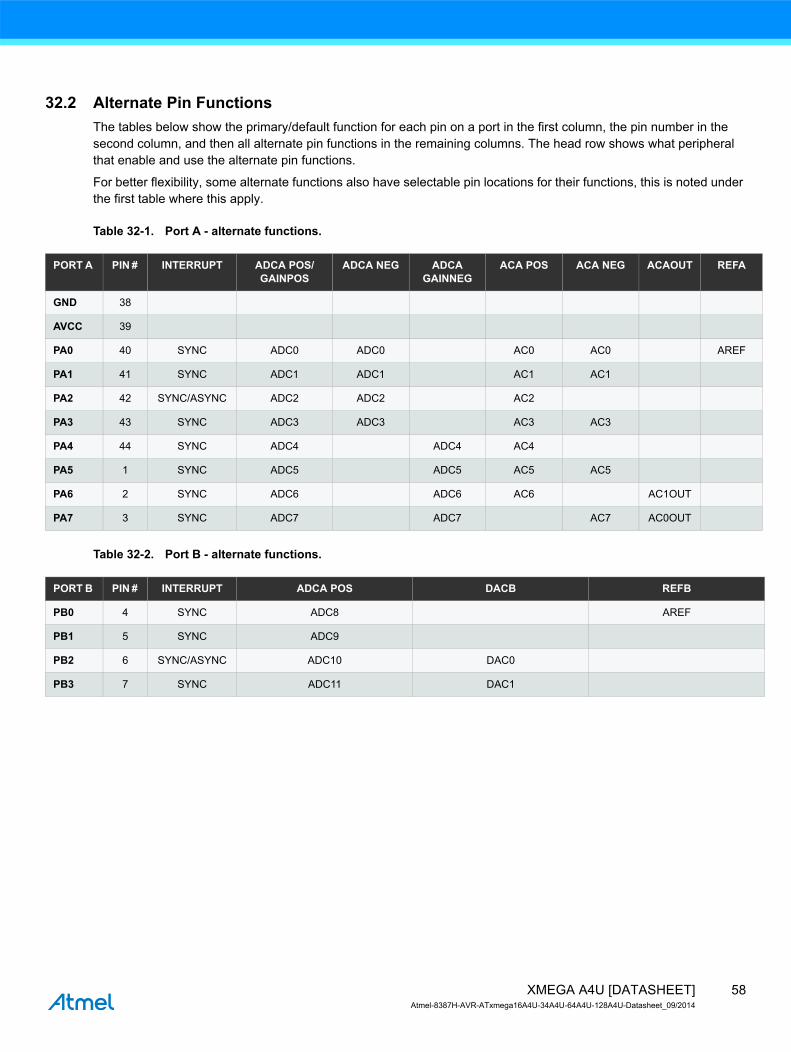
32.2 Alternate Pin FunctionsThe tables below show the primary/default function for each pin on a port in the first column, the pin number in the second column, and then all alternate pin functions in the remaining columns. The head row shows what peripheral that enable and use the alternate pin functions.
For better flexibility, some alternate functions also have selectable pin locations for their functions, this is noted under the first table where this apply.
Table 32-1. Port A - alternate functions.
Table 32-2. Port B - alternate functions.
PORT A PIN # INTERRUPT ADCA POS/ GAINPOS
ADCA NEG ADCA GAINNEG
ACA POS ACA NEG ACAOUT REFA
GND 38
AVCC 39
PA0 40 SYNC ADC0 ADC0 AC0 AC0 AREF
PA1 41 SYNC ADC1 ADC1 AC1 AC1
PA2 42 SYNC/ASYNC ADC2 ADC2 AC2
PA3 43 SYNC ADC3 ADC3 AC3 AC3
PA4 44 SYNC ADC4 ADC4 AC4
PA5 1 SYNC ADC5 ADC5 AC5 AC5
PA6 2 SYNC ADC6 ADC6 AC6 AC1OUT
PA7 3 SYNC ADC7 ADC7 AC7 AC0OUT
PORT B PIN # INTERRUPT ADCA POS DACB REFB
PB0 4 SYNC ADC8 AREF
PB1 5 SYNC ADC9
PB2 6 SYNC/ASYNC ADC10 DAC0
PB3 7 SYNC ADC11 DAC1
58XMEGA A4U [DATASHEET]Atmel-8387H-AVR-ATxmega16A4U-34A4U-64A4U-128A4U-Datasheet_09/2014

UT
T
T
Table 32-3. Port C - alternate functions.
Notes: 1. Pin mapping of all TC0 can optionally be moved to high nibble of port2. If TC0 is configured as TC2 all eight pins can be used for PWM output.3. Pin mapping of all USART0 can optionally be moved to high nibble of port.4. Pins MOSI and SCK for all SPI can optionally be swapped.5. CLKOUT can optionally be moved between port C, D and E and between pin 4 and 7.6. EVOUT can optionally be moved between port C, D and E and between pin 4 and 7.
Table 32-4. Port D - alternate functions.
PORT C PIN # INTERRUPT TCC0(1)(2)
AWEXC TCC1 USARTC0(3)
USARTC1
SPIC(4) TWIC TWIC w/ext driver
CLOCKOUT(5)
EVENTO(6)
GND 8
VCC 9
PC0 10 SYNC OC0A OC0ALS SDA SDAIN
PC1 11 SYNC OC0B OC0AHS XCK0 SCL SCLIN
PC2 12 SYNC/ASYNC OC0C OC0BLS RXD0 SDAOUT
PC3 13 SYNC OC0D OC0BHS TXD0 SCLOUT
PC4 14 SYNC OC0CLS OC1A SS
PC5 15 SYNC OC0CHS OC1B XCK1 MOSI
PC6 16 SYNC OC0DLS RXD1 MISO clkRTC
PC7 17 SYNC OC0DHS TXD1 SCK clkPER EVOU
PORT D PIN # INTERRUPT TCD0 TCD1 USB USARTD0 USARTD1 SPID CLOCKOUT EVENTOU
GND 18
VCC 19
PD0 20 SYNC OC0A
PD1 21 SYNC OC0B XCK0
PD2 22 SYNC/ASYNC OC0C RXD0
PD3 23 SYNC OC0D TXD0
PD4 24 SYNC OC1A SS
PD5 25 SYNC OC1B XCK1 MOSI
PD6 26 SYNC D- RXD1 MISO
PD7 27 SYNC D+ TXD1 SCK clkPER EVOUT
59XMEGA A4U [DATASHEET]Atmel-8387H-AVR-ATxmega16A4U-34A4U-64A4U-128A4U-Datasheet_09/2014

Table 32-5. Port E - alternate functions.
Table 32-6. Port R - alternate functions.
Note: 1. TOSC pins can optionally be moved to PE2/PE3.
PORT E PIN # INTERRUPT TCE0 USARTE0 TWIE
PE0 28 SYNC OC0A SDA
PE1 29 SYNC OC0B XCK0 SCL
GND 30
VCC 31
PE2 32 SYNC/ASYNC OC0C RXD0
PE3 33 SYNC OC0D TXD0
PORT R PIN # INTERRUPT PDI XTAL TOSC(1)
PDI 34 PDI_DATA
RESET 35 PDI_CLOCK
PR0 36 SYNC XTAL2 TOSC2
PR1 37 SYNC XTAL1 TOSC1
60XMEGA A4U [DATASHEET]Atmel-8387H-AVR-ATxmega16A4U-34A4U-64A4U-128A4U-Datasheet_09/2014

33. Peripheral Module Address MapThe address maps show the base address for each peripheral and module in Atmel AVR XMEGA A4U. For complete register description and summary for each peripheral module, refer to the XMEGA AU manual.
Table 33-1. Peripheral module address map.
Base address Name Description
0x0000 GPIO General Purpose IO Registers
0x0010 VPORT0 Virtual Port 0
0x0014 VPORT1 Virtual Port 1
0x0018 VPORT2 Virtual Port 2
0x001C VPORT3 Virtual Port 2
0x0030 CPU CPU
0x0040 CLK Clock Control
0x0048 SLEEP Sleep Controller
0x0050 OSC Oscillator Control
0x0060 DFLLRC32M DFLL for the 32MHz Internal RC Oscillator
0x0068 DFLLRC2M DFLL for the 2MHz RC Oscillator
0x0070 PR Power Reduction
0x0078 RST Reset Controller
0x0080 WDT Watch-Dog Timer
0x0090 MCU MCU Control
0x00A0 PMIC Programmable MUltilevel Interrupt Controller
0x00B0 PORTCFG Port Configuration
0x00C0 AES AES Module
0x00D0 CRC CRC Module
0x0100 DMA DMA Module
0x0180 EVSYS Event System
0x01C0 NVM Non Volatile Memory (NVM) Controller
0x0200 ADCA Analog to Digital Converter on port A
0x0380 ACA Analog Comparator pair on port A
0x0400 RTC Real Time Counter
0x0480 TWIC Two Wire Interface on port C
0x04A0 TWIE Two Wire Interface on port E
0x04C0 USB Universal Serial Bus Interface
0x0600 PORTA Port A
61XMEGA A4U [DATASHEET]Atmel-8387H-AVR-ATxmega16A4U-34A4U-64A4U-128A4U-Datasheet_09/2014

0x0620 PORTB Port B
0x0640 PORTC Port C
0x0660 PORTD Port D
0x0680 PORTE Port E
0x07E0 PORTR Port R
0x0800 TCC0 Timer/Counter 0 on port C
0x0840 TCC1 Timer/Counter 1 on port C
0x0880 AWEXC Advanced Waveform Extension on port C
0x0890 HIRESC High Resolution Extension on port C
0x08A0 USARTC0 USART 0 on port C
0x08B0 USARTC1 USART 1 on port C
0x08C0 SPIC Serial Peripheral Interface on port C
0x08F8 IRCOM Infrared Communication Module
0x0900 TCD0 Timer/Counter 0 on port D
0x0940 TCD1 Timer/Counter 1 on port D
0x0990 HIRESD High Resolution Extension on port D
0x09A0 USARTD0 USART 0 on port D
0x09B0 USARTD1 USART 1 on port D
0x09C0 SPID Serial Peripheral Interface on port D
0x0A00 TCE0 Timer/Counter 0 on port E
0x0A80 AWEXE Advanced Waveform Extensionon port E
0x0A90 HIRESE High Resolution Extension on port E
0x0AA0 USARTE0 USART 0 on port E
Base address Name Description
62XMEGA A4U [DATASHEET]Atmel-8387H-AVR-ATxmega16A4U-34A4U-64A4U-128A4U-Datasheet_09/2014

34. Instruction Set SummaryMnemonics
Operands Description Operation Flags
#Clocks
Arithmetic and Logic Instructions
ADD Rd, Rr Add without Carry Rd ← Rd + Rr Z,C,N,V,S,H 1
ADC Rd, Rr Add with Carry Rd ← Rd + Rr + C Z,C,N,V,S,H 1
ADIW Rd, K Add Immediate to Word Rd ← Rd + 1:Rd + K Z,C,N,V,S 2
SUB Rd, Rr Subtract without Carry Rd ← Rd - Rr Z,C,N,V,S,H 1
SUBI Rd, K Subtract Immediate Rd ← Rd - K Z,C,N,V,S,H 1
SBC Rd, Rr Subtract with Carry Rd ← Rd - Rr - C Z,C,N,V,S,H 1
SBCI Rd, K Subtract Immediate with Carry Rd ← Rd - K - C Z,C,N,V,S,H 1
SBIW Rd, K Subtract Immediate from Word Rd + 1:Rd ← Rd + 1:Rd - K Z,C,N,V,S 2
AND Rd, Rr Logical AND Rd ← Rd • Rr Z,N,V,S 1
ANDI Rd, K Logical AND with Immediate Rd ← Rd • K Z,N,V,S 1
OR Rd, Rr Logical OR Rd ← Rd v Rr Z,N,V,S 1
ORI Rd, K Logical OR with Immediate Rd ← Rd v K Z,N,V,S 1
EOR Rd, Rr Exclusive OR Rd ← Rd ⊕ Rr Z,N,V,S 1
COM Rd One’s Complement Rd ← $FF - Rd Z,C,N,V,S 1
NEG Rd Two’s Complement Rd ← $00 - Rd Z,C,N,V,S,H 1
SBR Rd,K Set Bit(s) in Register Rd ← Rd v K Z,N,V,S 1
CBR Rd,K Clear Bit(s) in Register Rd ← Rd • ($FFh - K) Z,N,V,S 1
INC Rd Increment Rd ← Rd + 1 Z,N,V,S 1
DEC Rd Decrement Rd ← Rd - 1 Z,N,V,S 1
TST Rd Test for Zero or Minus Rd ← Rd • Rd Z,N,V,S 1
CLR Rd Clear Register Rd ← Rd ⊕ Rd Z,N,V,S 1
SER Rd Set Register Rd ← $FF None 1
MUL Rd,Rr Multiply Unsigned R1:R0 ← Rd x Rr (UU) Z,C 2
MULS Rd,Rr Multiply Signed R1:R0 ← Rd x Rr (SS) Z,C 2
MULSU Rd,Rr Multiply Signed with Unsigned R1:R0 ← Rd x Rr (SU) Z,C 2
FMUL Rd,Rr Fractional Multiply Unsigned R1:R0 ← Rd x Rr<<1 (UU) Z,C 2
FMULS Rd,Rr Fractional Multiply Signed R1:R0 ← Rd x Rr<<1 (SS) Z,C 2
FMULSU Rd,Rr Fractional Multiply Signed with Unsigned R1:R0 ← Rd x Rr<<1 (SU) Z,C 2
DES K Data Encryption if (H = 0) then R15:R0else if (H = 1) then R15:R0
←←
Encrypt(R15:R0, K)Decrypt(R15:R0, K)
1/2
Branch instructions
RJMP k Relative Jump PC ← PC + k + 1 None 2
IJMP Indirect Jump to (Z) PC(15:0)PC(21:16)
←←
Z,0
None 2
EIJMP Extended Indirect Jump to (Z) PC(15:0)PC(21:16)
←←
Z,EIND
None 2
JMP k Jump PC ← k None 3
63XMEGA A4U [DATASHEET]Atmel-8387H-AVR-ATxmega16A4U-34A4U-64A4U-128A4U-Datasheet_09/2014

RCALL k Relative Call Subroutine PC ← PC + k + 1 None 2 / 3 (1)
ICALL Indirect Call to (Z) PC(15:0)PC(21:16)
←←
Z,0
None 2 / 3 (1)
EICALL Extended Indirect Call to (Z) PC(15:0)PC(21:16)
←←
Z,EIND
None 3 (1)
CALL k call Subroutine PC ← k None 3 / 4 (1)
RET Subroutine Return PC ← STACK None 4 / 5 (1)
RETI Interrupt Return PC ← STACK I 4 / 5 (1)
CPSE Rd,Rr Compare, Skip if Equal if (Rd = Rr) PC ← PC + 2 or 3 None 1 / 2 / 3
CP Rd,Rr Compare Rd - Rr Z,C,N,V,S,H 1
CPC Rd,Rr Compare with Carry Rd - Rr - C Z,C,N,V,S,H 1
CPI Rd,K Compare with Immediate Rd - K Z,C,N,V,S,H 1
SBRC Rr, b Skip if Bit in Register Cleared if (Rr(b) = 0) PC ← PC + 2 or 3 None 1 / 2 / 3
SBRS Rr, b Skip if Bit in Register Set if (Rr(b) = 1) PC ← PC + 2 or 3 None 1 / 2 / 3
SBIC A, b Skip if Bit in I/O Register Cleared if (I/O(A,b) = 0) PC ← PC + 2 or 3 None 2 / 3 / 4
SBIS A, b Skip if Bit in I/O Register Set If (I/O(A,b) =1) PC ← PC + 2 or 3 None 2 / 3 / 4
BRBS s, k Branch if Status Flag Set if (SREG(s) = 1) then PC ← PC + k + 1 None 1 / 2
BRBC s, k Branch if Status Flag Cleared if (SREG(s) = 0) then PC ← PC + k + 1 None 1 / 2
BREQ k Branch if Equal if (Z = 1) then PC ← PC + k + 1 None 1 / 2
BRNE k Branch if Not Equal if (Z = 0) then PC ← PC + k + 1 None 1 / 2
BRCS k Branch if Carry Set if (C = 1) then PC ← PC + k + 1 None 1 / 2
BRCC k Branch if Carry Cleared if (C = 0) then PC ← PC + k + 1 None 1 / 2
BRSH k Branch if Same or Higher if (C = 0) then PC ← PC + k + 1 None 1 / 2
BRLO k Branch if Lower if (C = 1) then PC ← PC + k + 1 None 1 / 2
BRMI k Branch if Minus if (N = 1) then PC ← PC + k + 1 None 1 / 2
BRPL k Branch if Plus if (N = 0) then PC ← PC + k + 1 None 1 / 2
BRGE k Branch if Greater or Equal, Signed if (N ⊕ V= 0) then PC ← PC + k + 1 None 1 / 2
BRLT k Branch if Less Than, Signed if (N ⊕ V= 1) then PC ← PC + k + 1 None 1 / 2
BRHS k Branch if Half Carry Flag Set if (H = 1) then PC ← PC + k + 1 None 1 / 2
BRHC k Branch if Half Carry Flag Cleared if (H = 0) then PC ← PC + k + 1 None 1 / 2
BRTS k Branch if T Flag Set if (T = 1) then PC ← PC + k + 1 None 1 / 2
BRTC k Branch if T Flag Cleared if (T = 0) then PC ← PC + k + 1 None 1 / 2
BRVS k Branch if Overflow Flag is Set if (V = 1) then PC ← PC + k + 1 None 1 / 2
BRVC k Branch if Overflow Flag is Cleared if (V = 0) then PC ← PC + k + 1 None 1 / 2
BRIE k Branch if Interrupt Enabled if (I = 1) then PC ← PC + k + 1 None 1 / 2
BRID k Branch if Interrupt Disabled if (I = 0) then PC ← PC + k + 1 None 1 / 2
Data transfer instructions
MOV Rd, Rr Copy Register Rd ← Rr None 1
Mnemonics
Operands Description Operation Flags
#Clocks
64XMEGA A4U [DATASHEET]Atmel-8387H-AVR-ATxmega16A4U-34A4U-64A4U-128A4U-Datasheet_09/2014
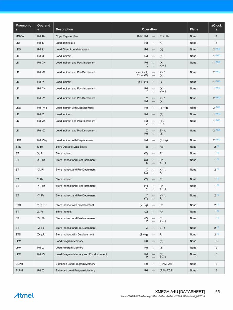
MOVW Rd, Rr Copy Register Pair Rd+1:Rd ← Rr+1:Rr None 1
LDI Rd, K Load Immediate Rd ← K None 1
LDS Rd, k Load Direct from data space Rd ← (k) None 2 (1)(2)
LD Rd, X Load Indirect Rd ← (X) None 1 (1)(2)
LD Rd, X+ Load Indirect and Post-Increment RdX
←←
(X)X + 1
None 1 (1)(2)
LD Rd, -X Load Indirect and Pre-Decrement X ← X - 1,Rd ← (X)
←←
X - 1(X)
None 2 (1)(2)
LD Rd, Y Load Indirect Rd ← (Y) ← (Y) None 1 (1)(2)
LD Rd, Y+ Load Indirect and Post-Increment RdY
←←
(Y)Y + 1
None 1 (1)(2)
LD Rd, -Y Load Indirect and Pre-Decrement YRd
←←
Y - 1(Y)
None 2 (1)(2)
LDD Rd, Y+q Load Indirect with Displacement Rd ← (Y + q) None 2 (1)(2)
LD Rd, Z Load Indirect Rd ← (Z) None 1 (1)(2)
LD Rd, Z+ Load Indirect and Post-Increment RdZ
←←
(Z),Z+1
None 1 (1)(2)
LD Rd, -Z Load Indirect and Pre-Decrement ZRd
←←
Z - 1,(Z)
None 2 (1)(2)
LDD Rd, Z+q Load Indirect with Displacement Rd ← (Z + q) None 2 (1)(2)
STS k, Rr Store Direct to Data Space (k) ← Rd None 2 (1)
ST X, Rr Store Indirect (X) ← Rr None 1 (1)
ST X+, Rr Store Indirect and Post-Increment (X)X
←←
Rr,X + 1
None 1 (1)
ST -X, Rr Store Indirect and Pre-Decrement X(X)
←←
X - 1,Rr
None 2 (1)
ST Y, Rr Store Indirect (Y) ← Rr None 1 (1)
ST Y+, Rr Store Indirect and Post-Increment (Y)Y
←←
Rr,Y + 1
None 1 (1)
ST -Y, Rr Store Indirect and Pre-Decrement Y(Y)
←←
Y - 1,Rr
None 2 (1)
STD Y+q, Rr Store Indirect with Displacement (Y + q) ← Rr None 2 (1)
ST Z, Rr Store Indirect (Z) ← Rr None 1 (1)
ST Z+, Rr Store Indirect and Post-Increment (Z)Z
←←
RrZ + 1
None 1 (1)
ST -Z, Rr Store Indirect and Pre-Decrement Z ← Z - 1 None 2 (1)
STD Z+q,Rr Store Indirect with Displacement (Z + q) ← Rr None 2 (1)
LPM Load Program Memory R0 ← (Z) None 3
LPM Rd, Z Load Program Memory Rd ← (Z) None 3
LPM Rd, Z+ Load Program Memory and Post-Increment RdZ
←←
(Z),Z + 1
None 3
ELPM Extended Load Program Memory R0 ← (RAMPZ:Z) None 3
ELPM Rd, Z Extended Load Program Memory Rd ← (RAMPZ:Z) None 3
Mnemonics
Operands Description Operation Flags
#Clocks
65XMEGA A4U [DATASHEET]Atmel-8387H-AVR-ATxmega16A4U-34A4U-64A4U-128A4U-Datasheet_09/2014

ELPM Rd, Z+ Extended Load Program Memory and Post-Increment
RdZ
←←
(RAMPZ:Z),Z + 1
None 3
SPM Store Program Memory (RAMPZ:Z) ← R1:R0 None -
SPM Z+ Store Program Memory and Post-Increment by 2
(RAMPZ:Z)Z
←←
R1:R0,Z + 2
None -
IN Rd, A In From I/O Location Rd ← I/O(A) None 1
OUT A, Rr Out To I/O Location I/O(A) ← Rr None 1
PUSH Rr Push Register on Stack STACK ← Rr None 1 (1)
POP Rd Pop Register from Stack Rd ← STACK None 2 (1)
XCH Z, Rd Exchange RAM location TempRd(Z)
←←←
Rd,(Z),Temp
None 2
LAS Z, Rd Load and Set RAM location TempRd(Z)
←←←
Rd,(Z),Temp v (Z)
None 2
LAC Z, Rd Load and Clear RAM location TempRd(Z)
←←←
Rd,(Z),($FFh – Rd) (Z)
None 2
LAT Z, Rd Load and Toggle RAM location TempRd(Z)
←←←
Rd,(Z),Temp ⊕ (Z)
None 2
Bit and bit-test instructions
LSL Rd Logical Shift Left Rd(n+1)Rd(0)
C
←←←
Rd(n),0,Rd(7)
Z,C,N,V,H 1
LSR Rd Logical Shift Right Rd(n)Rd(7)
C
←←←
Rd(n+1),0,Rd(0)
Z,C,N,V 1
ROL Rd Rotate Left Through Carry Rd(0)Rd(n+1)
C
←←←
C,Rd(n),Rd(7)
Z,C,N,V,H 1
ROR Rd Rotate Right Through Carry Rd(7)Rd(n)
C
←←←
C,Rd(n+1),Rd(0)
Z,C,N,V 1
ASR Rd Arithmetic Shift Right Rd(n) ← Rd(n+1), n=0..6 Z,C,N,V 1
SWAP Rd Swap Nibbles Rd(3..0) ↔ Rd(7..4) None 1
BSET s Flag Set SREG(s) ← 1 SREG(s) 1
BCLR s Flag Clear SREG(s) ← 0 SREG(s) 1
SBI A, b Set Bit in I/O Register I/O(A, b) ← 1 None 1
CBI A, b Clear Bit in I/O Register I/O(A, b) ← 0 None 1
BST Rr, b Bit Store from Register to T T ← Rr(b) T 1
BLD Rd, b Bit load from T to Register Rd(b) ← T None 1
SEC Set Carry C ← 1 C 1
CLC Clear Carry C ← 0 C 1
SEN Set Negative Flag N ← 1 N 1
CLN Clear Negative Flag N ← 0 N 1
SEZ Set Zero Flag Z ← 1 Z 1
Mnemonics
Operands Description Operation Flags
#Clocks
66XMEGA A4U [DATASHEET]Atmel-8387H-AVR-ATxmega16A4U-34A4U-64A4U-128A4U-Datasheet_09/2014

Notes: 1. Cycle times for Data memory accesses assume internal memory accesses, and are not valid for accesses via the external RAM interface.2. One extra cycle must be added when accessing Internal SRAM.
CLZ Clear Zero Flag Z ← 0 Z 1
SEI Global Interrupt Enable I ← 1 I 1
CLI Global Interrupt Disable I ← 0 I 1
SES Set Signed Test Flag S ← 1 S 1
CLS Clear Signed Test Flag S ← 0 S 1
SEV Set Two’s Complement Overflow V ← 1 V 1
CLV Clear Two’s Complement Overflow V ← 0 V 1
SET Set T in SREG T ← 1 T 1
CLT Clear T in SREG T ← 0 T 1
SEH Set Half Carry Flag in SREG H ← 1 H 1
CLH Clear Half Carry Flag in SREG H ← 0 H 1
MCU control instructions
BREAK Break (See specific descr. for BREAK) None 1
NOP No Operation None 1
SLEEP Sleep (see specific descr. for Sleep) None 1
WDR Watchdog Reset (see specific descr. for WDR) None 1
Mnemonics
Operands Description Operation Flags
#Clocks
67XMEGA A4U [DATASHEET]Atmel-8387H-AVR-ATxmega16A4U-34A4U-64A4U-128A4U-Datasheet_09/2014

35. Packaging information
35.1 44A
44A, 44-lead, 10 x 10mm body size, 1.0mm body thickness,0.8 mm lead pitch, thin profile plastic quad flat package (TQFP)
C44A
06/02/2014
PIN 1 IDENTIFIER
0°~7°
PIN 1
L
C
A1 A2 A
D1
D
e
E1 E
B
COMMON DIMENSIONS(Unit of Measure = mm)
SYMBOL MIN NOM MAX NOTE
Notes: 1. This package conforms to JEDEC reference MS-026, Variation ACB. 2. Dimensions D1 and E1 do not include mold protrusion. Allowable protrusion is 0.25mm per side. Dimensions D1 and E1 are maximum plastic body size dimensions including mold mismatch. 3. Lead coplanarity is 0.10mm maximum.
A – – 1.20
A1 0.05 – 0.15
A2 0.95 1.00 1.05
D 11.75 12.00 12.25
D1 9.90 10.00 10.10 Note 2
E 11.75 12.00 12.25
E1 9.90 10.00 10.10 Note 2
B 0.30 0.37 0.45
C 0.09 (0.17) 0.20
L 0.45 0.60 0.75
e 0.80 TYP
68XMEGA A4U [DATASHEET]Atmel-8387H-AVR-ATxmega16A4U-34A4U-64A4U-128A4U-Datasheet_09/2014

35.2 PW
69XMEGA A4U [DATASHEET]Atmel-8387H-AVR-ATxmega16A4U-34A4U-64A4U-128A4U-Datasheet_09/2014

35.3 44M1
TITLE DRAWING NO.GPC REV. Package Drawing Contact: [email protected] 44M1ZWS H
44M1, 44-pad, 7 x 7 x 1.0mm body, lead pitch 0.50mm, 5.20mm exposed pad, thermally enhanced plastic very thin quad flat no lead package (VQFN)
02/13/2014
COMMON DIMENSIONS(Unit of Measure = mm)
SYMBOL MIN NOM MAX NOT E
A 0.80 0.90 1.00
A1 – 0.02 0.05
A3 0.20 REF
b 0.18 0.23 0.30
D
D2 5.00 5.20 5.40
6.90 7.00 7.10
6.90 7.00 7.10
E
E2 5.00 5.20 5.40
e 0.50 BSC
L 0.59 0.64 0.69
K 0.20 0.26 0.41Note: JEDEC Standard MO-220, Fig . 1 (S AW Singulation) VKKD-3 .
TOP VIE W
SIDE VIEW
B OT TOM VIE W
D
E
Marked Pin# 1 I D
E2
D2
b e
Pin #1 Co rnerL
A1
A3
A
SE ATING PLAN E
Pin #1 Triangle
Pin #1 Cham fer(C 0.30)
Option A
Option B
Pin #1 Notch(0.20 R)
Option C
K
K
123
70XMEGA A4U [DATASHEET]Atmel-8387H-AVR-ATxmega16A4U-34A4U-64A4U-128A4U-Datasheet_09/2014

35.4 49C2
TITLE DRAWING NO.GPC REV. Package Drawing Contact: [email protected] 49C2CBD A
49C2, 49-ball (7 x 7 array), 0.65mm pitch, 5.0 x 5.0 x 1.0mm, very thin, fine-pitch ball grid array package (VFBGA)
3/14/08
COMMON DIMENSIONS(Unit of Measure = mm)
SYMBOL MIN NOM MAX NOTE
A – – 1.00
A1 0.20 – –
A2 0.65 – –
D 4.90 5.00 5.10
D1 3.90 BSC
E 4.90 5.00 5.10
E1 3.90 BSC
b 0.30 0.35 0.40
e 0.65 BSC
TOP VIEW
SIDE VIEW
A1 BALL ID
G
F
E
D
C
B
A
1 2 3 4 5 6 7
A
A1
A2
D
E0.10
E1
D1
49 - Ø0.35 ±0.05
e
A1 BALL CORNER
BOTTOM VIEW
b e
71XMEGA A4U [DATASHEET]Atmel-8387H-AVR-ATxmega16A4U-34A4U-64A4U-128A4U-Datasheet_09/2014

36. Electrical CharacteristicsAll typical values are measured at T = 25°C unless other temperature condition is given. All minimum and maximum values are valid across operating temperature and voltage unless other conditions are given.
36.1 ATxmega16A4U
36.1.1 Absolute Maximum Ratings
Stresses beyond those listed in Table 36-1 may cause permanent damage to the device. This is a stress rating only and functional operation of the device at these or other conditions beyond those indicated in the operational sections of this specification is not implied. Exposure to absolute maximum rating conditions for extended periods may affect device reliability.
Table 36-1. Absolute maximum ratings.
36.1.2 General Operating Ratings
The device must operate within the ratings listed in Table 36-2 in order for all other electrical characteristics and typical characteristics of the device to be valid.
Table 36-2. General operating conditions.
Symbol Parameter Condition Min. Typ. Max. Units
VCC Power supply voltage -0.3 4 V
IVCC Current into a VCC pin 200 mA
IGND Current out of a Gnd pin 200 mA
VPIN Pin voltage with respect to Gnd and VCC -0.5 VCC+0.5 V
IPIN I/O pin sink/source current -25 25 mA
TA Storage temperature -65 150 °C
Tj Junction temperature 150 °C
Symbol Parameter Condition Min. Typ. Max. Units
VCC Power supply voltage 1.60 3.6 V
AVCC Analog supply voltage 1.60 3.6 V
TA Temperature range -40 85 °C
Tj Junction temperature -40 105 °C
72XMEGA A4U [DATASHEET]Atmel-8387H-AVR-ATxmega16A4U-34A4U-64A4U-128A4U-Datasheet_09/2014

Table 36-3. Operating voltage and frequency.
The maximum CPU clock frequency depends on VCC. As shown in Figure 36-1 the Frequency vs. VCC curve is linear between 1.8V < VCC < 2.7V.
Figure 36-1. Maximum Frequency vs. VCC.
Symbol Parameter Condition Min. Typ. Max. Units
ClkCPU CPU clock frequency
VCC = 1.6V 0 12
MHzVCC = 1.8V 0 12
VCC = 2.7V 0 32
VCC = 3.6V 0 32
1.8
12
32
MHz
V2.7 3.61.6
Safe Operating Area
73XMEGA A4U [DATASHEET]Atmel-8387H-AVR-ATxmega16A4U-34A4U-64A4U-128A4U-Datasheet_09/2014

36.1.3 Current consumption
Table 36-4. Current consumption for Active mode and sleep modes.
Notes: 1. All Power Reduction Registers set.2. Maximum limits are based on characterization, and not tested in production.
Symbol Parameter Condition Min. Typ. Max. Units
ICC
Active powerconsumption (1)
32kHz, Ext. ClkVCC = 1.8V 40
µA
VCC = 3.0V 80
1MHz, Ext. ClkVCC = 1.8V 230
VCC = 3.0V 480
2MHz, Ext. ClkVCC = 1.8V 430 600
VCC = 3.0V0.9 1.4
mA32MHz, Ext. Clk 9.6 12
Idle powerconsumption (1)
32kHz, Ext. ClkVCC = 1.8V 2.4
µA
VCC = 3.0V 3.9
1MHz, Ext. ClkVCC = 1.8V 62
VCC = 3.0V 118
2MHz, Ext. ClkVCC = 1.8V 125 225
VCC = 3.0V240 350
32MHz, Ext. Clk 3.8 5.5 mA
Power-down powerconsumption
T = 25°C
VCC = 3.0V
0.1 1.0
µA
T = 85°C 1.2 4.5
T = 105°C 3.5 6.0
WDT and Sampled BOD enabled,T = 25°C
VCC = 3.0V
1.3 3.0
WDT and Sampled BOD enabled,T = 85°C 2.4 6.0
WDT and Sampled BOD enabled,T = 105°C 4.5 8.0
Power-save powerconsumption (2)
RTC from ULP clock, WDT and sampledBOD enabled, T = 25°C
VCC = 1.8V 1.2
µA
VCC = 3.0V 1.3
RTC from 1.024kHz low power32.768kHz TOSC, T = 25°C
VCC = 1.8V 0.6 2.0
VCC = 3.0V 0.7 2.0
RTC from low power 32.768kHz TOSC,T = 25°C
VCC = 1.8V 0.8 3.0
VCC = 3.0V 1.0 3.0
Reset power consumption Current through RESET pin substracted VCC = 3.0V 320 µA
74XMEGA A4U [DATASHEET]Atmel-8387H-AVR-ATxmega16A4U-34A4U-64A4U-128A4U-Datasheet_09/2014

Table 36-5. Current consumption for modules and peripherals.
Note: 1. All parameters measured as the difference in current consumption between module enabled and disabled. All data at VCC = 3.0V, ClkSYS = 1MHz external clock without prescaling, T = 25°C unless other conditions are given.
Symbol Parameter Condition (1) Min. Typ. Max. Units
ICC
ULP oscillator 1.0 µA
32.768kHz int. oscillator 27 µA
2MHz int. oscillator85
µADFLL enabled with 32.768kHz int. osc. as reference 115
32MHz int. oscillator270
µADFLL enabled with 32.768kHz int. osc. as reference 460
PLL20x multiplication factor,
32MHz int. osc. DIV4 as reference220 µA
Watchdog timer 1.0 µA
BODContinuous mode 138
µASampled mode, includes ULP oscillator 1.2
Internal 1.0V reference 100 µA
Temperature sensor 95 µA
ADC 250kspsVREF = Ext ref
3.0
mACURRLIMIT = LOW 2.6
CURRLIMIT = MEDIUM 2.1
CURRLIMIT = HIGH 1.6
DAC250kspsVREF = Ext refNo load
Normal mode 1.9mA
Low Power mode 1.1
ACHigh speed mode 330
µALow power mode 130
DMA 615kbps between I/O registers and SRAM 108 µA
Timer/counter 16 µA
USART Rx and Tx enabled, 9600 BAUD 2.5 µA
Flash memory and EEPROM programming 4.0 8.0 mA
75XMEGA A4U [DATASHEET]Atmel-8387H-AVR-ATxmega16A4U-34A4U-64A4U-128A4U-Datasheet_09/2014

36.1.4 Wake-up time from sleep modes
Table 36-6. Device wake-up time from sleep modes with various system clock sources.
Note: 1. The wake-up time is the time from the wake-up request is given until the peripheral clock is available on pin, see Figure 36-2. All peripherals and modules start execution from the first clock cycle, expect the CPU that is halted for four clock cycles before program execution starts.
Figure 36-2. Wake-up time definition.
Symbol Parameter Condition Min. Typ. (1) Max. Units
twakeup
Wake-up time from idle, standby, and extended standby mode
External 2MHz clock 2.0
µs
32.768kHz internal oscillator 120
2MHz internal oscillator 2.0
32MHz internal oscillator 0.2
Wake-up time from power-save and power-down mode
External 2MHz clock 4.5
32.768kHz internal oscillator 320
2MHz internal oscillator 9.0
32MHz internal oscillator 5.0
Wakeup request
Clock output
Wakeup time
76XMEGA A4U [DATASHEET]Atmel-8387H-AVR-ATxmega16A4U-34A4U-64A4U-128A4U-Datasheet_09/2014

36.1.5 I/O Pin Characteristics
The I/O pins comply with the JEDEC LVTTL and LVCMOS specification and the high- and low level input and output voltage limits reflect or exceed this specification.
Table 36-7. I/O pin characteristics.
Notes: 1. The sum of all IOH for PORTA and PORTB must not exceed 100mA.The sum of all IOH for PORTC must not exceed 200mA.The sum of all IOH for PORTD and pins PE[0-1] on PORTE must not exceed 200mA.The sum of all IOH for PE[2-3] on PORTE, PORTR and PDI must not exceed 100mA.
2. The sum of all IOL for PORTA and PORTB must not exceed 100mA.The sum of all IOL for PORTC must not exceed 200mA.The sum of all IOL for PORTD and pins PE[0-1] on PORTE must not exceed 200mA.The sum of all IOL for PE[2-3] on PORTE, PORTR and PDI must not exceed 100mA.
Symbol Parameter Condition Min. Typ. Max. Units
IOH (1)/
IOL (2) I/O pin source/sink current -20 20 mA
VIH High level input voltage
VCC = 2.7 - 3.6V 2.0 VCC+0.3
VVCC = 2.0 - 2.7V 0.7*VCC VCC+0.3
VCC = 1.6 - 2.0V 0.8*VCC VCC+0.3
VIL Low level input voltage
VCC = 2.7- 3.6V -0.3 0.8
VVCC = 2.0 - 2.7V -0.3 0.3*VCC
VCC = 1.6 - 2.0V -0.3 0.2*VCC
VOH High level output voltage
VCC = 3.0 - 3.6V IOH = -2mA 2.4 0.94*VCC
V
VCC = 2.3 - 2.7VIOH = -1mA 2.0 0.96*VCC
IOH = -2mA 1.7 0.92*VCC
VCC = 3.3V IOH = -8mA 2.6 2.9
VCC = 3.0V IOH = -6mA 2.1 2.6
VCC = 1.8V IOH = -2mA 1.4 1.6
VOL Low level output voltage
VCC = 3.0 - 3.6V IOL = 2mA 0.05*VCC 0.4
V
VCC = 2.3 - 2.7VIOL = 1mA 0.03*VCC 0.4
IOL = 2mA 0.06*VCC 0.7
VCC = 3.3V IOL = 15mA 0.4 0.76
VCC = 3.0V IOL = 10mA 0.3 0.64
VCC = 1.8V IOL = 5mA 0.2 0.46
IIN Input leakage current T = 25°C <0.01 0.1 µA
RP Pull/buss keeper resistor 24 kΩ
tr Rise time No load4.0
nsslew rate limitation 7.0
77XMEGA A4U [DATASHEET]Atmel-8387H-AVR-ATxmega16A4U-34A4U-64A4U-128A4U-Datasheet_09/2014

36.1.6 ADC characteristics
Table 36-8. Power supply, reference and input range.
Table 36-9. Clock and timing.
Symbol Parameter Condition Min. Typ. Max. Units
AVCC Analog supply voltage VCC- 0.3 VCC+ 0.3 V
VREF Reference voltage 1.0 AVCC- 0.6 V
Rin Input resistance Switched 4.0 kΩ
Csample Input capacitance Switched 4.4 pF
RAREF Reference input resistance (leakage only) >10 MΩ
CAREF Reference input capacitance Static load 7.0 pF
VIN Input range -0.1 AVCC+0.1 V
Conversion range Differential mode, Vinp - Vinn -VREF VREF V
Conversion range Single ended unsigned mode, Vinp -ΔV VREF-ΔV V
∆V Fixed offset voltage 190 LSB
Symbol Parameter Condition Min. Typ. Max. Units
ClkADC ADC Clock frequency
Maximum is 1/4 of peripheral clock frequency 100 2000
kHz
Measuring internal signals 100 125
fADC Sample rate
Current limitation (CURRLIMIT) off 100 2000
kspsCURRLIMIT = LOW 100 1500
CURRLIMIT = MEDIUM 100 1000
CURRLIMIT = HIGH 100 500
Sampling time 1/2 ClkADC cycle 0.25 5 µs
Conversion time (latency) (RES+2)/2+(GAIN !=0)RES (Resolution) = 8 or 12 5 8 ClkADC
cycles
Start-up time ADC clock cycles 12 24 ClkADCcycles
ADC settling timeAfter changing reference or input mode 7 7 ClkADC
cyclesAfter ADC flush 1 1
78XMEGA A4U [DATASHEET]Atmel-8387H-AVR-ATxmega16A4U-34A4U-64A4U-128A4U-Datasheet_09/2014
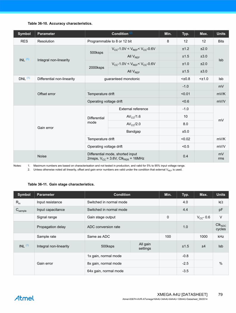
Table 36-10. Accuracy characteristics.
Notes: 1. Maximum numbers are based on characterisation and not tested in production, and valid for 5% to 95% input voltage range.2. Unless otherwise noted all linearity, offset and gain error numbers are valid under the condition that external VREF is used.
Table 36-11. Gain stage characteristics.
Symbol Parameter Condition (2) Min. Typ. Max. Units
RES Resolution Programmable to 8 or 12 bit 8 12 12 Bits
INL (1) Integral non-linearity
500kspsVCC-1.0V < VREF< VCC-0.6V ±1.2 ±2.0
lsbAll VREF ±1.5 ±3.0
2000kspsVCC-1.0V < VREF< VCC-0.6V ±1.0 ±2.0
All VREF ±1.5 ±3.0
DNL (1) Differential non-linearity guaranteed monotonic <±0.8 <±1.0 lsb
Offset error
-1.0 mV
Temperature drift <0.01 mV/K
Operating voltage drift <0.6 mV/V
Gain error
Differentialmode
External reference -1.0
mVAVCC/1.6 10
AVCC/2.0 8.0
Bandgap ±5.0
Temperature drift <0.02 mV/K
Operating voltage drift <0.5 mV/V
Noise Differential mode, shorted input2msps, VCC = 3.6V, ClkPER = 16MHz 0.4 mV
rms
Symbol Parameter Condition Min. Typ. Max. Units
Rin Input resistance Switched in normal mode 4.0 kΩ
Csample Input capacitance Switched in normal mode 4.4 pF
Signal range Gain stage output 0 VCC- 0.6 V
Propagation delay ADC conversion rate 1.0 ClkADCcycles
Sample rate Same as ADC 100 1000 kHz
INL (1) Integral non-linearity 500ksps All gainsettings ±1.5 ±4 lsb
Gain error
1x gain, normal mode -0.8
%8x gain, normal mode -2.5
64x gain, normal mode -3.5
79XMEGA A4U [DATASHEET]Atmel-8387H-AVR-ATxmega16A4U-34A4U-64A4U-128A4U-Datasheet_09/2014

Note: 1. Maximum numbers are based on characterisation and not tested in production, and valid for 5% to 95% input voltage range.
36.1.7 DAC Characteristics
Table 36-12. Power supply, reference and output range.
Offset error,input referred
1x gain, normal mode -2
mV8x gain, normal mode -5
64x gain, normal mode -4
Noise
1x gain, normal modeVCC = 3.6VExt. VREF
0.5mV rms8x gain, normal mode 1.5
64x gain, normal mode 11
Symbol Parameter Condition Min. Typ. Max. Units
Symbol Parameter Condition Min. Typ. Max. Units
AVCC Analog supply voltage VCC- 0.3 VCC+ 0.3 V
AVREF External reference voltage 1.0 VCC- 0.6 V
Rchannel DC output impedance 50 Ω
Linear output voltage range 0.15 AVCC-0.15 V
RAREF Reference input resistance >10 MΩ
CAREF Reference input capacitance Static load 7 pF
Minimum resistance load 1.0 kΩ
Maximum capacitance load100 pF
1000Ω serial resistance 1.0 nF
Output sink/sourceOperating within accuracy specification AVCC/1000
mASafe operation 10
80XMEGA A4U [DATASHEET]Atmel-8387H-AVR-ATxmega16A4U-34A4U-64A4U-128A4U-Datasheet_09/2014

Table 36-13. Clock and timing.
Table 36-14. Accuracy characteristics.
Note: 1. Maximum numbers are based on characterisation and not tested in production, and valid for 5% to 95% output voltage range.
Symbol Parameter Condition Min. Typ. Max. Units
fDAC Conversion rate Cload=100pF, maximum step size
Normal mode 0 1000ksps
Low power mode 500
Symbol Parameter Condition Min. Typ. Max. Units
RES Input resolution 12 Bits
INL (1) Integral non-linearity
VREF= Ext 1.0VVCC = 1.6V ±2.0 ±3
lsb
VCC = 3.6V ±1.5 ±2.5
VREF=AVCC
VCC = 1.6V ±2.0 ±4
VCC = 3.6V ±1.5 ±4
VREF=INT1VVCC = 1.6V ±5.0
VCC = 3.6V ±5.0
DNL (1) Differential non-linearity
VREF=Ext 1.0VVCC = 1.6V ±1.5 3.0
lsb
VCC = 3.6V ±0.6 1.5
VREF=AVCC
VCC = 1.6V ±1.0 3.5
VCC = 3.6V ±0.6 1.5
VREF=INT1VVCC = 1.6V ±4.5
VCC = 3.6V ±4.5
Gain error After calibration <4.0 lsb
Gain calibration step size 4.0 lsb
Gain calibration drift VREF= Ext 1.0V <0.2 mV/K
Offset error After calibration <1.0 lsb
Offset calibration step size 1.0
81XMEGA A4U [DATASHEET]Atmel-8387H-AVR-ATxmega16A4U-34A4U-64A4U-128A4U-Datasheet_09/2014

36.1.8 Analog Comparator Characteristics
Table 36-15. Analog Comparator characteristics.
36.1.9 Bandgap and Internal 1.0V Reference Characteristics
Table 36-16. Bandgap and Internal 1.0V reference characteristics.
Symbol Parameter Condition Min. Typ. Max. Units
Voff Input offset voltage <±10 mV
Ilk Input leakage current <1.0 nA
Input voltage range -0.1 AVCC V
AC startup time 100 µs
Vhys1 Hysteresis, none 0 mV
Vhys2 Hysteresis, smallmode = High Speed (HS) 13
mVmode = Low Power (LP) 30
Vhys3 Hysteresis, largemode = HS 30
mVmode = LP 60
tdelay Propagation delay
VCC = 3.0V, T= 85°C mode = HS 30 90
nsmode = HS 30
VCC = 3.0V, T= 85°C mode = LP 130 500
mode = LP 130
64-level voltage scaler Integral non-linearity (INL) 0.3 0.5 lsb
Symbol Parameter Condition Min. Typ. Max. Units
Startup timeAs reference for ADC or DAC 1 ClkPER + 2.5µs
µsAs input voltage to ADC and AC 1.5
Bandgap voltage 1.1 V
INT1V Internal 1.00V reference T= 85°C, after calibration 0.99 1.0 1.01 V
Variation over voltage and temperature Relative to T= 85°C, VCC = 3.0V ±1.5 %
82XMEGA A4U [DATASHEET]Atmel-8387H-AVR-ATxmega16A4U-34A4U-64A4U-128A4U-Datasheet_09/2014
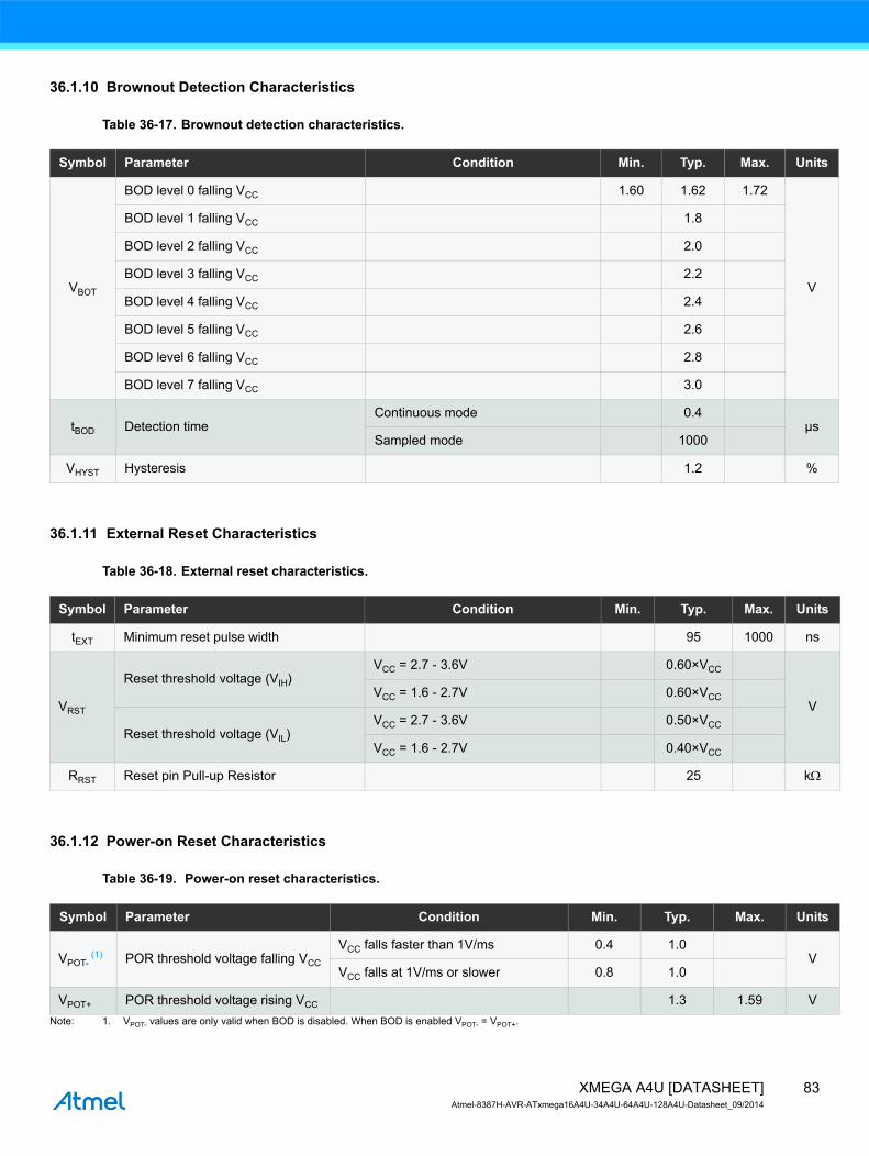
36.1.10 Brownout Detection Characteristics
Table 36-17. Brownout detection characteristics.
36.1.11 External Reset Characteristics
Table 36-18. External reset characteristics.
36.1.12 Power-on Reset Characteristics
Table 36-19. Power-on reset characteristics.
Note: 1. VPOT- values are only valid when BOD is disabled. When BOD is enabled VPOT- = VPOT+.
Symbol Parameter Condition Min. Typ. Max. Units
VBOT
BOD level 0 falling VCC 1.60 1.62 1.72
V
BOD level 1 falling VCC 1.8
BOD level 2 falling VCC 2.0
BOD level 3 falling VCC 2.2
BOD level 4 falling VCC 2.4
BOD level 5 falling VCC 2.6
BOD level 6 falling VCC 2.8
BOD level 7 falling VCC 3.0
tBOD Detection timeContinuous mode 0.4
µsSampled mode 1000
VHYST Hysteresis 1.2 %
Symbol Parameter Condition Min. Typ. Max. Units
tEXT Minimum reset pulse width 95 1000 ns
VRST
Reset threshold voltage (VIH)VCC = 2.7 - 3.6V 0.60×VCC
VVCC = 1.6 - 2.7V 0.60×VCC
Reset threshold voltage (VIL)VCC = 2.7 - 3.6V 0.50×VCC
VCC = 1.6 - 2.7V 0.40×VCC
RRST Reset pin Pull-up Resistor 25 kΩ
Symbol Parameter Condition Min. Typ. Max. Units
VPOT- (1) POR threshold voltage falling VCC
VCC falls faster than 1V/ms 0.4 1.0V
VCC falls at 1V/ms or slower 0.8 1.0
VPOT+ POR threshold voltage rising VCC 1.3 1.59 V
83XMEGA A4U [DATASHEET]Atmel-8387H-AVR-ATxmega16A4U-34A4U-64A4U-128A4U-Datasheet_09/2014

36.1.13 Flash and EEPROM Memory Characteristics
Table 36-20. Endurance and data retention.
Table 36-21. Programming time.
Notes: 1. Programming is timed from the 2MHz internal oscillator.2. EEPROM is not erased if the EESAVE fuse is programmed.
Symbol Parameter Condition Min. Typ. Max. Units
Flash
Write/Erase cycles
25°C 10K
Cycle85°C 10K
105°C 2K
Data retention
25°C 100
Year85°C 25
105°C 10
EEPROM
Write/Erase cycles
25°C 100K
Cycle85°C 100K
105°C 30K
Data retention
25°C 100
Year85°C 25
105°C 10
Symbol Parameter Condition Min. Typ.(1) Max. Units
Chip Erase 16KB Flash, EEPROM(2) and SRAM Erase 45 ms
Application Erase Section erase 6 ms
Flash
Page erase 4
msPage write 4
Atomic page erase and write 8
EEPROM
Page erase 4
msPage write 4
Atomic page erase and write 8
84XMEGA A4U [DATASHEET]Atmel-8387H-AVR-ATxmega16A4U-34A4U-64A4U-128A4U-Datasheet_09/2014

36.1.14 Clock and Oscillator Characteristics
36.1.14.1 Calibrated 32.768kHz Internal Oscillator characteristics
Table 36-22. 32.768kHz internal oscillator characteristics.
36.1.14.2 Calibrated 2MHz RC Internal Oscillator characteristics
Table 36-23. 2MHz internal oscillator characteristics.
36.1.14.3 Calibrated and tunable 32MHz internal oscillator characteristics
Table 36-24. 32MHz internal oscillator characteristics.
36.1.14.4 32kHz Internal ULP Oscillator characteristics
Table 36-25. 32kHz internal ULP oscillator characteristics.
Symbol Parameter Condition Min. Typ. Max. Units
Frequency 32.768 kHz
Factory calibration accuracy T = 85°C, VCC = 3.0V -0.5 0.5 %
User calibration accuracy -0.5 0.5 %
Symbol Parameter Condition Min. Typ. Max. Units
Frequency range DFLL can tune to this frequency over voltage and temperature 1.8 2.2 MHz
Factory calibrated frequency 2.0 MHz
Factory calibration accuracy T = 85°C, VCC= 3.0V -1.5 1.5 %
User calibration accuracy -0.2 0.2 %
DFLL calibration stepsize 0.21 %
Symbol Parameter Condition Min. Typ. Max. Units
Frequency range DFLL can tune to this frequency over voltage and temperature 30 55 MHz
Factory calibrated frequency 32 MHz
Factory calibration accuracy T = 85°C, VCC= 3.0V -1.5 1.5 %
User calibration accuracy -0.2 0.2 %
DFLL calibration step size 0.22 %
Symbol Parameter Condition Min. Typ. Max. Units
Output frequency 32 kHz
Accuracy -30 30 %
85XMEGA A4U [DATASHEET]Atmel-8387H-AVR-ATxmega16A4U-34A4U-64A4U-128A4U-Datasheet_09/2014

36.1.14.5 Internal Phase Locked Loop (PLL) characteristics
Table 36-26. Internal PLL characteristics.
Note: 1. The maximum output frequency vs. supply voltage is linear between 1.8V and 2.7V, and can never be higher than four times the maximum CPU frequency.
36.1.14.6 External clock characteristics
Figure 36-3. External clock drive waveform
Table 36-27. External clock used as system clock without prescaling.
Note: 1. The maximum frequency vs. supply voltage is linear between 1.6V and 2.7V, and the same applies for all other parameters with supply voltage conditions.
Symbol Parameter Condition Min. Typ. Max. Units
fIN Input frequency Output frequency must be within fOUT 0.4 64 MHz
fOUT Output frequency (1)VCC= 1.6 - 1.8V 20 48
MHzVCC= 2.7 - 3.6V 20 128
Start-up time 25 µs
Re-lock time 25 µs
tCH
tCL
tCK
tCH
VIL1
VIH1
tCR tCF
Symbol Parameter Condition Min. Typ. Max. Units
1/tCK Clock Frequency (1)VCC = 1.6 - 1.8V 0 12
MHzVCC = 2.7 - 3.6V 0 32
tCK Clock PeriodVCC = 1.6 - 1.8V 83.3
nsVCC = 2.7 - 3.6V 31.5
tCH Clock High TimeVCC = 1.6 - 1.8V 30.0
nsVCC = 2.7 - 3.6V 12.5
tCL Clock Low TimeVCC = 1.6 - 1.8V 30.0
nsVCC = 2.7 - 3.6V 12.5
tCR Rise Time (for maximum frequency)VCC = 1.6 - 1.8V 10
nsVCC = 2.7 - 3.6V 3
tCF Fall Time (for maximum frequency)VCC = 1.6 - 1.8V 10
nsVCC = 2.7 - 3.6V 3
ΔtCK Change in period from one clock cycle to the next 10 %
86XMEGA A4U [DATASHEET]Atmel-8387H-AVR-ATxmega16A4U-34A4U-64A4U-128A4U-Datasheet_09/2014

its
s
s
Table 36-28. External clock with prescaler (1)for system clock.
Notes: 1. System Clock Prescalers must be set so that maximum CPU clock frequency for device is not exceeded.2. The maximum frequency vs. supply voltage is linear between 1.6V and 2.7V, and the same applies for all other parameters with supply voltage conditions.
36.1.14.7 External 16MHz crystal oscillator and XOSC characteristic
Table 36-29. External 16MHz crystal oscillator and XOSC characteristics.
Symbol Parameter Condition Min. Typ. Max. Units
1/tCK Clock Frequency (2)VCC = 1.6 - 1.8V 0 90
MHzVCC = 2.7 - 3.6V 0 142
tCK Clock PeriodVCC = 1.6 - 1.8V 11
nsVCC = 2.7 - 3.6V 7
tCH Clock High TimeVCC = 1.6 - 1.8V 4.5
nsVCC = 2.7 - 3.6V 2.4
tCL Clock Low TimeVCC = 1.6 - 1.8V 4.5
nsVCC = 2.7 - 3.6V 2.4
tCR Rise Time (for maximum frequency)VCC = 1.6 - 1.8V 1.5
nsVCC = 2.7 - 3.6V 1.0
tCF Fall Time (for maximum frequency)VCC = 1.6 - 1.8V 1.5
nsVCC = 2.7 - 3.6V 1.0
ΔtCK Change in period from one clock cycle to the next 10 %
Symbol Parameter Condition Min. Typ. Max. Un
Cycle to cycle jitterXOSCPWR=0
FRQRANGE=0 <10
nFRQRANGE=1, 2, or 3 <1.0
XOSCPWR=1 <1.0
Long term jitterXOSCPWR=0
FRQRANGE=0 <6.0
nFRQRANGE=1, 2, or 3 <0.5
XOSCPWR=1 <0.5
Frequency errorXOSCPWR=0
FRQRANGE=0 <0.1
%FRQRANGE=1 <0.05
FRQRANGE=2 or 3 <0.005
XOSCPWR=1 <0.005
87XMEGA A4U [DATASHEET]Atmel-8387H-AVR-ATxmega16A4U-34A4U-64A4U-128A4U-Datasheet_09/2014

its
Note: 1. Numbers for negative impedance are not tested in production but guaranteed from design and characterization.
Duty cycleXOSCPWR=0
FRQRANGE=0 40
%FRQRANGE=1 42
FRQRANGE=2 or 3 45
XOSCPWR=1 48
RQ Negative impedance (1)
XOSCPWR=0,FRQRANGE=0
0.4MHz resonator, CL=100pF 2.4k
Ω
1MHz crystal, CL=20pF 8.7k
2MHz crystal, CL=20pF 2.1k
XOSCPWR=0,FRQRANGE=1,CL=20pF
2MHz crystal 4.2k
8MHz crystal 250
9MHz crystal 195
XOSCPWR=0,FRQRANGE=2,CL=20pF
8MHz crystal 360
9MHz crystal 285
12MHz crystal 155
XOSCPWR=0,FRQRANGE=3,CL=20pF
9MHz crystal 365
12MHz crystal 200
16MHz crystal 105
XOSCPWR=1,FRQRANGE=0,CL=20pF
9MHz crystal 435
12MHz crystal 235
16MHz crystal 125
XOSCPWR=1,FRQRANGE=1,CL=20pF
9MHz crystal 495
12MHz crystal 270
16MHz crystal 145
XOSCPWR=1,FRQRANGE=2,CL=20pF
12MHz crystal 305
16MHz crystal 160
XOSCPWR=1,FRQRANGE=3,CL=20pF
12MHz crystal 380
16MHz crystal 205
ESR SF = Safety factor min(RQ)/SF kΩ
CXTAL1Parasitic capacitance XTAL1 pin 5.4 pF
CXTAL2Parasitic capacitance XTAL2 pin 7.1 pF
CLOADParasitic capacitance load 3.07 pF
Symbol Parameter Condition Min. Typ. Max. Un
88XMEGA A4U [DATASHEET]Atmel-8387H-AVR-ATxmega16A4U-34A4U-64A4U-128A4U-Datasheet_09/2014

36.1.14.8 External 32.768kHz crystal oscillator and TOSC characteristics
Table 36-30. External 32.768kHz crystal oscillator and TOSC characteristics.
Note: 1. See Figure 36-4 for definition.
Figure 36-4. TOSC input capacitance.
The parasitic capacitance between the TOSC pins is CL1 + CL2 in series as seen from the crystal when oscillating without external capacitors.
Symbol Parameter Condition Min. Typ. Max. Units
ESR/R1 Recommended crystal equivalent series resistance (ESR)
Crystal load capacitance 6.5pF 60kΩ
Crystal load capacitance 9.0pF 35
CTOSC1 Parasitic capacitance TOSC1 pin5.4
pFAlternate TOSC location 4.0
CTOSC2 Parasitic capacitance TOSC2 pin7.1
pFAlternate TOSC location 4.0
Recommended safety factor capacitance load matched to crystal specification 3
CL1 CL2
2CSOT1CSOT Device internalExternal
32.768kHz crystal
89XMEGA A4U [DATASHEET]Atmel-8387H-AVR-ATxmega16A4U-34A4U-64A4U-128A4U-Datasheet_09/2014

36.1.15 SPI Characteristics
Figure 36-5. SPI timing requirements in master mode.
Figure 36-6. SPI timing requirements in slave mode.
MSB LSB
MSB LSB
tMOS
tMIS tMIH
tSCKW
tSCK
tMOH tMOH
tSCKFtSCKR
tSCKW
MOSI(Data output)
MISO(Data input)
SCK(CPOL = 1)
SCK(CPOL = 0)
SS
MSB LSB
MSB LSB
tSIS tSIH
tSSCKW
tSSCKW
tSSCK
tSSH
tSOSSH
tSCKR tSCKF
tSOS
tSSS
tSOSSS
MISO(Data output)
MOSI(Data input)
SCK(CPOL = 1)
SCK(CPOL = 0)
SS
90XMEGA A4U [DATASHEET]Atmel-8387H-AVR-ATxmega16A4U-34A4U-64A4U-128A4U-Datasheet_09/2014

Table 36-31. SPI timing characteristics and requirements.
36.1.16 Two-Wire Interface Characteristics
Table 36-32 on page 92 describes the requirements for devices connected to the Two-Wire Interface Bus. The Atmel AVR XMEGA Two-Wire Interface meets or exceeds these requirements under the noted conditions. Timing symbols refer to Figure 36-7 on page 91.
Figure 36-7. Two-wire interface bus timing.
Symbol Parameter Condition Min. Typ. Max. Units
tSCK SCK period Master (See Table 21-4 in XMEGA AU Manual)
ns
tSCKW SCK high/low width Master 0.5*SCK
tSCKR SCK rise time Master 2.7
tSCKF SCK fall time Master 2.7
tMIS MISO setup to SCK Master 10
tMIH MISO hold after SCK Master 10
tMOS MOSI setup SCK Master 0.5*SCK
tMOH MOSI hold after SCK Master 1
tSSCK Slave SCK Period Slave 4*t ClkPER
tSSCKW SCK high/low width Slave 2*t ClkPER
tSSCKR SCK rise time Slave 1600
tSSCKF SCK fall time Slave 1600
tSIS MOSI setup to SCK Slave 3
tSIH MOSI hold after SCK Slave t ClkPER
tSSS SS setup to SCK Slave 21
tSSH SS hold after SCK Slave 20
tSOS MISO setup SCK Slave 8
tSOH MISO hold after SCK Slave 13
tSOSS MISO setup after SS low Slave 11
tSOSH MISO hold after SS high Slave 8
tHD;STA
tof
SDA
SCL
tLOWtHIGH
tSU;STA
tBUF
tr
tHD;DAT tSU;DATtSU;STO
91XMEGA A4U [DATASHEET]Atmel-8387H-AVR-ATxmega16A4U-34A4U-64A4U-128A4U-Datasheet_09/2014

Table 36-32. Two-wire interface characteristics.
Notes: 1. Required only for fSCL > 100kHz.2. Cb = Capacitance of one bus line in pF.3. fPER = Peripheral clock frequency.
Symbol Parameter Condition Min. Typ. Max. Units
VIH Input high voltage 0.7*VCC VCC+0.5 V
VIL Input low voltage 0.5 0.3*VCC V
Vhys Hysteresis of Schmitt trigger inputs 0.05*VCC (1) V
VOL Output low voltage 3mA, sink current 0 0.4 V
tr Rise time for both SDA and SCL 20+0.1Cb (1)(2) 300 ns
tof Output fall time from VIHmin to VILmax 10pF < Cb < 400pF (2) 20+0.1Cb (1)(2) 250 ns
tSP Spikes suppressed by input filter 0 50 ns
II Input current for each I/O Pin 0.1VCC < VI < 0.9VCC -10 10 µA
CI Capacitance for each I/O Pin 10 pF
fSCL SCL clock frequency fPER (3)>max(10fSCL, 250kHz) 0 400 kHz
RP Value of pull-up resistor
fSCL ≤ 100kHz
ΩfSCL > 100kHz
tHD;STA Hold time (repeated) START conditionfSCL ≤ 100kHz 4.0
µsfSCL > 100kHz 0.6
tLOW Low period of SCL clockfSCL ≤ 100kHz 4.7
µsfSCL > 100kHz 1.3
tHIGH High period of SCL clockfSCL ≤ 100kHz 4.0
µsfSCL > 100kHz 0.6
tSU;STASet-up time for a repeated START condition
fSCL ≤ 100kHz 4.7µs
fSCL > 100kHz 0.6
tHD;DAT Data hold timefSCL ≤ 100kHz 0 3.45
µsfSCL > 100kHz 0 0.9
tSU;DAT Data setup timefSCL ≤ 100kHz 250
nsfSCL > 100kHz 100
tSU;STO Setup time for STOP conditionfSCL ≤ 100kHz 4.0
µsfSCL > 100kHz 0.6
tBUFBus free time between a STOP and START condition
fSCL ≤ 100kHz 4.7µs
fSCL > 100kHz 1.3
VCC 0.4V–3mA
----------------------------
100nsCb---------------
300nsCb---------------
92XMEGA A4U [DATASHEET]Atmel-8387H-AVR-ATxmega16A4U-34A4U-64A4U-128A4U-Datasheet_09/2014

36.2 ATxmega32A4U
36.2.1 Absolute Maximum Ratings
Stresses beyond those listed in Table 36-33 may cause permanent damage to the device. This is a stress rating only and functional operation of the device at these or other conditions beyond those indicated in the operational sections of this specification is not implied. Exposure to absolute maximum rating conditions for extended periods may affect device reliability.
Table 36-33. Absolute maximum ratings.
36.2.2 General Operating Ratings
The device must operate within the ratings listed in Table 36-34 in order for all other electrical characteristics and typical characteristics of the device to be valid.
Table 36-34. General operating conditions.
Table 36-35. Operating voltage and frequency.
The maximum CPU clock frequency depends on VCC. As shown in Figure 36-8 the Frequency vs. VCC curve is linear between 1.8V < VCC < 2.7V.
Symbol Parameter Condition Min. Typ. Max. Units
VCC Power supply voltage -0.3 4 V
IVCC Current into a VCC pin 200 mA
IGND Current out of a Gnd pin 200 mA
VPIN Pin voltage with respect to Gnd and VCC -0.5 VCC+0.5 V
IPIN I/O pin sink/source current -25 25 mA
TA Storage temperature -65 150 °C
Tj Junction temperature 150 °C
Symbol Parameter Condition Min. Typ. Max. Units
VCC Power supply voltage 1.60 3.6 V
AVCC Analog supply voltage 1.60 3.6 V
TA Temperature range -40 85 °C
Tj Junction temperature -40 105 °C
Symbol Parameter Condition Min. Typ. Max. Units
ClkCPU CPU clock frequency
VCC = 1.6V 0 12
MHzVCC = 1.8V 0 12
VCC = 2.7V 0 32
VCC = 3.6V 0 32
93XMEGA A4U [DATASHEET]Atmel-8387H-AVR-ATxmega16A4U-34A4U-64A4U-128A4U-Datasheet_09/2014

Figure 36-8. Maximum Frequency vs. VCC.
1.8
12
32
MHz
V2.7 3.61.6
Safe Operating Area
94XMEGA A4U [DATASHEET]Atmel-8387H-AVR-ATxmega16A4U-34A4U-64A4U-128A4U-Datasheet_09/2014

36.2.3 Current consumption
Table 36-36. Current consumption for Active mode and sleep modes.
Notes: 1. All Power Reduction Registers set.2. Maximum limits are based on characterization, and not tested in production.
Symbol Parameter Condition Min. Typ. Max. Units
ICC
Active power consumption(1)
32kHz, Ext. ClkVCC = 1.8V 40
µA
VCC = 3.0V 80
1MHz, Ext. ClkVCC = 1.8V 230
VCC = 3.0V 480
2MHz, Ext. ClkVCC = 1.8V 430 600
VCC = 3.0V0.9 1.4
mA32MHz, Ext. Clk 9.6 12
Idle powerconsumption(1)
32kHz, Ext. ClkVCC = 1.8V 2.4
µA
VCC = 3.0V 3.9
1MHz, Ext. ClkVCC = 1.8V 62
VCC = 3.0V 118
2MHz, Ext. ClkVCC = 1.8V 125 225
VCC = 3.0V240 350
32MHz, Ext. Clk 3.8 5.5 mA
Power-down power consumption
T = 25°C
VCC = 3.0V
0.1 1.0
µA
T = 85°C 1.2 4.5
T = 105°C 3.5 6.0
WDT and sampled BOD enabled, T = 25°C
VCC = 3.0V
1.3 3.0
WDT and sampled BOD enabled,T = 85°C 2.4 6.0
WDT and sampled BOD enabled,T = 105°C 4.5 8.0
Power-save power consumption(2)
RTC from ULP clock, WDT and sampled BOD enabled, T = 25°C
VCC = 1.8V 1.2
µA
VCC = 3.0V 1.3
RTC from 1.024kHz low power 32.768kHz TOSC, T = 25°C
VCC = 1.8V 0.6 2.0
VCC = 3.0V 0.7 2.0
RTC from low power 32.768kHz TOSC, T = 25°C
VCC = 1.8V 0.8 3.0
VCC = 3.0V 1.0 3.0
Reset power consumption Current through RESET pin substracted VCC = 3.0V 320
95XMEGA A4U [DATASHEET]Atmel-8387H-AVR-ATxmega16A4U-34A4U-64A4U-128A4U-Datasheet_09/2014

Table 36-37. Current consumption for modules and peripherals.
Note: 1. All parameters measured as the difference in current consumption between module enabled and disabled. All data at VCC = 3.0V, ClkSYS = 1MHz external clock without prescaling, T = 25°C unless other conditions are given.
Symbol Parameter Condition (1) Min. Typ. Max. Units
ICC
ULP oscillator 1.0 µA
32.768kHz int. oscillator 27 µA
2MHz int. oscillator85
µADFLL enabled with 32.768kHz int. osc. as reference 115
32MHz int. oscillator270
µADFLL enabled with 32.768kHz int. osc. as reference 460
PLL20x multiplication factor,
32MHz int. osc. DIV4 as reference220 µA
Watchdog timer 1.0 µA
BODContinuous mode 138
µASampled mode, includes ULP oscillator 1.2
Internal 1.0V reference 100 µA
Temperature sensor 95 µA
ADC 250kspsVREF = Ext ref
3.0
mACURRLIMIT = LOW 2.6
CURRLIMIT = MEDIUM 2.1
CURRLIMIT = HIGH 1.6
DAC250kspsVREF = Ext refNo load
Normal mode 1.9mA
Low power mode 1.1
ACHigh speed mode 330
µALow power mode 130
DMA 615kbps between I/O registers and SRAM 108 µA
Timer/counter 16 µA
USART Rx and Tx enabled, 9600 BAUD 2.5 µA
Flash memory and EEPROM programming 4.0 8.0 mA
96XMEGA A4U [DATASHEET]Atmel-8387H-AVR-ATxmega16A4U-34A4U-64A4U-128A4U-Datasheet_09/2014

36.2.4 Wake-up time from sleep modes
Table 36-38. Device wake-up time from sleep modes with various system clock sources.
Note: 1. The wake-up time is the time from the wake-up request is given until the peripheral clock is available on pin, see Figure 36-9. All peripherals and modules start execution from the first clock cycle, expect the CPU that is halted for four clock cycles before program execution starts.
Figure 36-9. Wake-up time definition.
Symbol Parameter Condition Min. Typ. (1) Max. Units
twakeup
Wake-up time from idle, standby, and extended standby mode
External 2MHz clock 2.0
µs32.768kHz internal oscillator 120
2MHz internal oscillator 2.0
32MHz internal oscillator 0.2
Wake-up time from power-save and power-down mode
External 2MHz clock 4.5
µs32.768kHz internal oscillator 320
2MHz internal oscillator 9.0
32MHz internal oscillator 5.0
Wakeup request
Clock output
Wakeup time
97XMEGA A4U [DATASHEET]Atmel-8387H-AVR-ATxmega16A4U-34A4U-64A4U-128A4U-Datasheet_09/2014

36.2.5 I/O Pin Characteristics
The I/O pins comply with the JEDEC LVTTL and LVCMOS specification and the high- and low level input and output voltage limits reflect or exceed this specification.
Table 36-39. I/O pin characteristics.
Notes: 1. The sum of all IOH for PORTA and PORTB must not exceed 100mA.The sum of all IOH for PORTC must not exceed 200mA.The sum of all IOH for PORTD and pins PE[0-1] on PORTE must not exceed 200mA.The sum of all IOH for PE[2-3] on PORTE, PORTR and PDI must not exceed 100mA.
2. The sum of all IOL for PORTA and PORTB must not exceed 100mA.The sum of all IOL for PORTC must not exceed 200mA.The sum of all IOL for PORTD and pins PE[0-1] on PORTE must not exceed 200mA.The sum of all IOL for PE[2-3] on PORTE, PORTR and PDI must not exceed 100mA.
Symbol Parameter Condition Min. Typ. Max. Units
IOH (1)/
IOL (2) I/O pin source/sink current -20 20 mA
VIH High level input voltage
VCC = 2.7 - 3.6V 2.0 VCC+0.3
VVCC = 2.0 - 2.7V 0.7*VCC VCC+0.3
VCC = 1.6 - 2.0V 0.8*VCC VCC+0.3
VIL Low level input voltage
VCC = 2.7- 3.6V -0.3 0.8
VVCC = 2.0 - 2.7V -0.3 0.3*VCC
VCC = 1.6 - 2.0V -0.3 0.2*VCC
VOH High level output voltage
VCC = 3.0 - 3.6V IOH = -2mA 2.4 0.94*VCC
V
VCC = 2.3 - 2.7VIOH = -1mA 2.0 0.96*VCC
IOH = -2mA 1.7 0.92*VCC
VCC = 3.3V IOH = -8mA 2.6 2.9
VCC = 3.0V IOH = -6mA 2.1 2.6
VCC = 1.8V IOH = -2mA 1.4 1.6
VOL Low level output voltage
VCC = 3.0 - 3.6V IOL = 2mA 0.05*VCC 0.4
V
VCC = 2.3 - 2.7VIOL = 1mA 0.03*VCC 0.4
IOL = 2mA 0.06*VCC 0.7
VCC = 3.3V IOL = 15mA 0.4 0.76
VCC = 3.0V IOL = 10mA 0.3 0.64
VCC = 1.8V IOL = 5mA 0.2 0.46
IIN Input leakage current T = 25°C <0.01 0.1 µA
RP Pull/buss keeper resistor 24 kΩ
tr Rise time No load4.0
nsslew rate limitation 7.0
98XMEGA A4U [DATASHEET]Atmel-8387H-AVR-ATxmega16A4U-34A4U-64A4U-128A4U-Datasheet_09/2014

36.2.6 ADC characteristics
Table 36-40. Power supply, reference and input range.
Table 36-41. Clock and timing.
Symbol Parameter Condition Min. Typ. Max. Units
AVCC Analog supply voltage VCC- 0.3 VCC+ 0.3 V
VREF Reference voltage 1 AVCC- 0.6 V
Rin Input resistance Switched 4.0 kΩ
Csample Input capacitance Switched 4.4 pF
RAREF Reference input resistance (leakage only) >10 MΩ
CAREF Reference input capacitance Static load 7 pF
VIN Input range -0.1 AVCC+0.1 V
Conversion range Differential mode, Vinp - Vinn -VREF VREF V
Conversion range Single ended unsigned mode, Vinp -ΔV VREF-ΔV V
∆V Fixed offset voltage 190 LSB
Symbol Parameter Condition Min. Typ. Max. Units
ClkADC ADC clock frequency
Maximum is 1/4 of peripheral clock frequency 100 2000
kHz
Measuring internal signals 100 125
fADC Sample rate
Current limitation (CURRLIMIT) off 100 2000
kspsCURRLIMIT = LOW 100 1500
CURRLIMIT = MEDIUM 100 1000
CURRLIMIT = HIGH 100 500
Sampling time 1/2 ClkADC cycle 0.25 5 µs
Conversion time (latency) (RES+2)/2+(GAIN !=0)RES (Resolution) = 8 or 12 5 8 ClkADC
cycles
Start-up time ADC clock cycles 12 24 ClkADCcycles
ADC settling timeAfter changing reference or input mode 7 7 ClkADC
cyclesAfter ADC flush 1 1
99XMEGA A4U [DATASHEET]Atmel-8387H-AVR-ATxmega16A4U-34A4U-64A4U-128A4U-Datasheet_09/2014

Table 36-42. Accuracy characteristics.
Notes: 1. Maximum numbers are based on characterisation and not tested in production, and valid for 5% to 95% input voltage range.2. Unless otherwise noted all linearity, offset and gain error numbers are valid under the condition that external VREF is used.
Table 36-43. Gain stage characteristics.
Symbol Parameter Condition (2) Min. Typ. Max. Units
RES Resolution Programmable to 8 or 12 bit 8 12 12 Bits
INL(1) Integral non-linearity
500kspsVCC-1.0V < VREF< VCC-0.6V ±1.2 ±2.0
lsbAll VREF ±1.5 ±3.0
2000kspsVCC-1.0V < VREF< VCC-0.6V ±1.0 ±2.0
All VREF ±1.5 ±3.0
DNL(1) Differential non-linearity guaranteed monotonic <±0.8 <±1.0 lsb
Offset error
-1.0 mV
Temperature drift <0.01 mV/K
Operating voltage drift <0.6 mV/V
Gain error
Differential mode
External reference -1.0
mVAVCC/1.6 10
AVCC/2.0 8.0
Bandgap ±5.0
Temperature drift <0.02 mV/K
Operating voltage drift <0.5 mV/V
Noise Differential mode, shorted input2msps, VCC = 3.6V, ClkPER = 16MHz 0.4 mV
rms
Symbol Parameter Condition Min. Typ. Max. Units
Rin Input resistance Switched in normal mode 4.0 kΩ
Csample Input capacitance Switched in normal mode 4.4 pF
Signal range Gain stage output 0 VCC- 0.6 V
Propagation delay ADC conversion rate 1.0 ClkADCcycles
Sample rate Same as ADC 100 1000 kHz
INL (1) Integral non-linearity 500ksps All gain settings ±1.5 ±4.0 lsb
Gain error
1x gain, normal mode -0.8
%8x gain, normal mode -2.5
64x gain, normal mode -3.5
100XMEGA A4U [DATASHEET]Atmel-8387H-AVR-ATxmega16A4U-34A4U-64A4U-128A4U-Datasheet_09/2014

Note: 1. Maximum numbers are based on characterisation and not tested in production, and valid for 5% to 95% input voltage range.
36.2.7 DAC Characteristics
Table 36-44. Power supply, reference and output range.
Table 36-45. Clock and timing.
Offset error,input referred
1x gain, normal mode -2.0
mV8x gain, normal mode -5.0
64x gain, normal mode -4.0
Noise
1x gain, normal modeVCC = 3.6V
Ext. VREF
0.5mV rms8x gain, normal mode 1.5
64x gain, normal mode 11
Symbol Parameter Condition Min. Typ. Max. Units
Symbol Parameter Condition Min. Typ. Max. Units
AVCC Analog supply voltage VCC- 0.3 VCC+ 0.3 V
AVREF External reference voltage 1.0 VCC- 0.6 V
Rchannel DC output impedance 50 Ω
Linear output voltage range 0.15 AVCC-0.15 V
RAREF Reference input resistance >10 MΩ
CAREF Reference input capacitance Static load 7.0 pF
Minimum Resistance load 1.0 kΩ
Maximum capacitance load100 pF
1000Ω serial resistance 1.0 nF
Output sink/sourceOperating within accuracy specification AVCC/1000
mASafe operation 10
Symbol Parameter Condition Min. Typ. Max. Units
fDAC Conversion rate Cload=100pF, maximum step size
Normal mode 0 1000ksps
Low power mode 500
101XMEGA A4U [DATASHEET]Atmel-8387H-AVR-ATxmega16A4U-34A4U-64A4U-128A4U-Datasheet_09/2014

Table 36-46. Accuracy characteristics.
Note: 1. Maximum numbers are based on characterisation and not tested in production, and valid for 5% to 95% output voltage range.
Symbol Parameter Condition Min. Typ. Max. Units
RES Input resolution 12 Bits
INL (1) Integral non-linearity
VREF= Ext 1.0VVCC = 1.6V ±2.0 ±3.0
lsb
VCC = 3.6V ±1.5 ±2.5
VREF=AVCC
VCC = 1.6V ±2.0 ±4.0
VCC = 3.6V ±1.5 ±4.0
VREF=INT1VVCC = 1.6V ±5.0
VCC = 3.6V ±5.0
DNL (1) Differential non-linearity
VREF=Ext 1.0VVCC = 1.6V ±1.5 3.0
lsb
VCC = 3.6V ±0.6 1.5
VREF=AVCC
VCC = 1.6V ±1.0 3.5
VCC = 3.6V ±0.6 1.5
VREF=INT1VVCC = 1.6V ±4.5
VCC = 3.6V ±4.5
Gain error After calibration <4.0 lsb
Gain calibration step size 4.0 lsb
Gain calibration drift VREF= Ext 1.0V <0.2 mV/K
Offset error After calibration <1.0 lsb
Offset calibration step size 1.0
102XMEGA A4U [DATASHEET]Atmel-8387H-AVR-ATxmega16A4U-34A4U-64A4U-128A4U-Datasheet_09/2014

36.2.8 Analog Comparator Characteristics
Table 36-47. Analog Comparator characteristics.
36.2.9 Bandgap and Internal 1.0V Reference Characteristics
Table 36-48. Bandgap and Internal 1.0V reference characteristics.
Symbol Parameter Condition Min. Typ. Max. Units
Voff Input offset voltage <±10 mV
Ilk Input leakage current <1 nA
Input voltage range -0.1 AVCC V
AC startup time 100 µs
Vhys1 Hysteresis, none 0 mV
Vhys2 Hysteresis, smallmode = High Speed (HS) 13
mVmode = Low Power (LP) 30
Vhys3 Hysteresis, largemode = HS 30
mVmode = LP 60
tdelay Propagation delay
VCC = 3.0V, T= 85°C mode = HS 30 90
nsmode = HS 30
VCC = 3.0V, T= 85°C mode = LP 130 500
mode = LP 130
64-level voltage scaler Integral non-linearity (INL) 0.3 0.5 lsb
Symbol Parameter Condition Min. Typ. Max. Units
Startup timeAs reference for ADC or DAC 1 ClkPER + 2.5µs
µsAs input voltage to ADC and AC 1.5
Bandgap voltage 1.1 V
INT1V Internal 1.00V reference T= 85°C, after calibration 0.99 1.0 1.01 V
Variation over voltage and temperature Relative to T= 85°C, VCC = 3.0V ±1.5 %
103XMEGA A4U [DATASHEET]Atmel-8387H-AVR-ATxmega16A4U-34A4U-64A4U-128A4U-Datasheet_09/2014

36.2.10 Brownout Detection Characteristics
Table 36-49. Brownout detection characteristics.
36.2.11 External Reset Characteristics
Table 36-50. External reset characteristics.
36.2.12 Power-on Reset Characteristics
Table 36-51. Power-on reset characteristics.
Note: 1. VPOT- values are only valid when BOD is disabled. When BOD is enabled VPOT- = VPOT+.
Symbol Parameter Condition Min. Typ. Max. Units
VBOT
BOD level 0 falling VCC 1.60 1.62 1.72
V
BOD level 1 falling VCC 1.8
BOD level 2 falling VCC 2.0
BOD level 3 falling VCC 2.2
BOD level 4 falling VCC 2.4
BOD level 5 falling VCC 2.6
BOD level 6 falling VCC 2.8
BOD level 7 falling VCC 3.0
tBOD Detection timeContinuous mode 0.4
µsSampled mode 1000
VHYST Hysteresis 1.2 %
Symbol Parameter Condition Min. Typ. Max. Units
tEXT Minimum reset pulse width 95 1000 ns
VRST
Reset threshold voltage (VIH)VCC = 2.7 - 3.6V 0.60*VCC
VVCC = 1.6 - 2.7V 0.60*VCC
Reset threshold voltage (VIL)VCC = 2.7 - 3.6V 0.50*VCC
VCC = 1.6 - 2.7V 0.40*VCC
RRST Reset pin Pull-up Resistor 25 kΩ
Symbol Parameter Condition Min. Typ. Max. Units
VPOT- (1) POR threshold voltage falling VCC
VCC falls faster than 1V/ms 0.4 1.0V
VCC falls at 1V/ms or slower 0.8 1.0
VPOT+ POR threshold voltage rising VCC 1.3 1.59 V
104XMEGA A4U [DATASHEET]Atmel-8387H-AVR-ATxmega16A4U-34A4U-64A4U-128A4U-Datasheet_09/2014

36.2.13 Flash and EEPROM Memory Characteristics
Table 36-52. Endurance and data retention.
Table 36-53. Programming time.
Notes: 1. Programming is timed from the 2MHz internal oscillator.2. EEPROM is not erased if the EESAVE fuse is programmed.
Symbol Parameter Condition Min. Typ. Max. Units
Flash
Write/Erase cycles
25°C 10K
Cycle85°C 10K
105°C 2K
Data retention
25°C 100
Year85°C 25
105°C 10
EEPROM
Write/Erase cycles
25°C 100K
Cycle85°C 100K
105°C 30K
Data retention
25°C 100
Year85°C 25
105°C 10
Symbol Parameter Condition Min. Typ.(1) Max. Units
Chip Erase 32KB Flash, EEPROM(2) and SRAM erase 50 ms
Application Erase Section erase 6 ms
Flash
Page erase 4
msPage write 4
Atomic page erase and write 8
EEPROM
Page erase 4
msPage write 4
Atomic page erase and write 8
105XMEGA A4U [DATASHEET]Atmel-8387H-AVR-ATxmega16A4U-34A4U-64A4U-128A4U-Datasheet_09/2014

36.2.14 Clock and Oscillator Characteristics
36.2.14.1 Calibrated 32.768kHz Internal Oscillator characteristics
Table 36-54. 32.768kHz internal oscillator characteristics.
36.2.14.2 Calibrated 2MHz RC Internal Oscillator characteristics
Table 36-55. 2MHz internal oscillator characteristics.
36.2.14.3 Calibrated and tunable 32MHz internal oscillator characteristics
Table 36-56. 32MHz internal oscillator characteristics.
36.2.14.4 32kHz Internal ULP Oscillator characteristics
Table 36-57. 32kHz internal ULP oscillator characteristics.
Symbol Parameter Condition Min. Typ. Max. Units
Frequency 32.768 kHz
Factory calibration accuracy T = 85°C, VCC = 3.0V -0.5 0.5 %
User calibration accuracy -0.5 0.5 %
Symbol Parameter Condition Min. Typ. Max. Units
Frequency range DFLL can tune to this frequency over voltage and temperature 1.8 2.2 MHz
Factory calibrated frequency 2.0 MHz
Factory calibration accuracy T = 85°C, VCC= 3.0V -1.5 1.5 %
User calibration accuracy -0.2 0.2 %
DFLL calibration stepsize 0.21 %
Symbol Parameter Condition Min. Typ. Max. Units
Frequency range DFLL can tune to this frequency over voltage and temperature 30 55 MHz
Factory calibrated frequency 32 MHz
Factory calibration accuracy T = 85°C, VCC= 3.0V -1.5 1.5 %
User calibration accuracy -0.2 0.2 %
DFLL calibration step size 0.22 %
Symbol Parameter Condition Min. Typ. Max. Units
Output frequency 32 kHz
Accuracy -30 30 %
106XMEGA A4U [DATASHEET]Atmel-8387H-AVR-ATxmega16A4U-34A4U-64A4U-128A4U-Datasheet_09/2014

36.2.14.5 Internal Phase Locked Loop (PLL) characteristics
Table 36-58. Internal PLL characteristics.
Note: 1. The maximum output frequency vs. supply voltage is linear between 1.8V and 2.7V, and can never be higher than four times the maximum CPU frequency.
36.2.14.6 External clock characteristics
Figure 36-10. External clock drive waveform
Table 36-59. External clock used as system clock without prescaling.
Note: 1. The maximum frequency vs. supply voltage is linear between 1.6V and 2.7V, and the same applies for all other parameters with supply voltage conditions.
Symbol Parameter Condition Min. Typ. Max. Units
fIN Input frequency Output frequency must be within fOUT 0.4 64 MHz
fOUT Output frequency (1)VCC= 1.6 - 1.8V 20 48
MHzVCC= 2.7 - 3.6V 20 128
Start-up time 25 µs
Re-lock time 25 µs
tCH
tCL
tCK
tCH
VIL1
VIH1
tCR tCF
Symbol Parameter Condition Min. Typ. Max. Units
1/tCK Clock Frequency (1)VCC = 1.6 - 1.8V 0 12
MHzVCC = 2.7 - 3.6V 0 32
tCK Clock PeriodVCC = 1.6 - 1.8V 83.3
nsVCC = 2.7 - 3.6V 31.5
tCH Clock High TimeVCC = 1.6 - 1.8V 30.0
nsVCC = 2.7 - 3.6V 12.5
tCL Clock Low TimeVCC = 1.6 - 1.8V 30.0
nsVCC = 2.7 - 3.6V 12.5
tCR Rise Time (for maximum frequency)VCC = 1.6 - 1.8V 10
nsVCC = 2.7 - 3.6V 3
tCF Fall Time (for maximum frequency)VCC = 1.6 - 1.8V 10
nsVCC = 2.7 - 3.6V 3
ΔtCK Change in period from one clock cycle to the next 10 %
107XMEGA A4U [DATASHEET]Atmel-8387H-AVR-ATxmega16A4U-34A4U-64A4U-128A4U-Datasheet_09/2014

Table 36-60. External clock with prescaler (1)for system clock.
Notes: 1. System Clock Prescalers must be set so that maximum CPU clock frequency for device is not exceeded.2. The maximum frequency vs. supply voltage is linear between 1.6V and 2.7V, and the same applies for all other parameters with supply voltage conditions.
36.2.14.7 External 16MHz crystal oscillator and XOSC characteristic
Table 36-61. External 16MHz crystal oscillator and XOSC characteristics.
Symbol Parameter Condition Min. Typ. Max. Units
1/tCK Clock Frequency (2)VCC = 1.6 - 1.8V 0 90
MHzVCC = 2.7 - 3.6V 0 142
tCK Clock PeriodVCC = 1.6 - 1.8V 11
nsVCC = 2.7 - 3.6V 7
tCH Clock High TimeVCC = 1.6 - 1.8V 4.5
nsVCC = 2.7 - 3.6V 2.4
tCL Clock Low TimeVCC = 1.6 - 1.8V 4.5
nsVCC = 2.7 - 3.6V 2.4
tCR Rise Time (for maximum frequency)VCC = 1.6 - 1.8V 1.5
nsVCC = 2.7 - 3.6V 1.0
tCF Fall Time (for maximum frequency)VCC = 1.6 - 1.8V 1.5
nsVCC = 2.7 - 3.6V 1.0
ΔtCK Change in period from one clock cycle to the next 10 %
Symbol Parameter Condition Min. Typ. Max. Units
Cycle to cycle jitterXOSCPWR=0
FRQRANGE=0 <10
nsFRQRANGE=1, 2, or 3 <1
XOSCPWR=1 <1
Long term jitterXOSCPWR=0
FRQRANGE=0 <6
nsFRQRANGE=1, 2, or 3 <0.5
XOSCPWR=1 <0.5
Frequency errorXOSCPWR=0
FRQRANGE=0 <0.1
%FRQRANGE=1 <0.05
FRQRANGE=2 or 3 <0.005
XOSCPWR=1 <0.005
Duty cycleXOSCPWR=0
FRQRANGE=0 40
%FRQRANGE=1 42
FRQRANGE=2 or 3 45
XOSCPWR=1 48
108XMEGA A4U [DATASHEET]Atmel-8387H-AVR-ATxmega16A4U-34A4U-64A4U-128A4U-Datasheet_09/2014

Note: 1. Numbers for negative impedance are not tested in production but guaranteed from design and characterization.
RQNegative impedance (1)
XOSCPWR=0,FRQRANGE=0
0.4MHz resonator, CL=100pF 2.4k
Ω
1MHz crystal, CL=20pF 8.7k
2MHz crystal, CL=20pF 2.1k
XOSCPWR=0,FRQRANGE=1,CL=20pF
2MHz crystal 4.2k
8MHz crystal 250
9MHz crystal 195
XOSCPWR=0,FRQRANGE=2,CL=20pF
8MHz crystal 360
9MHz crystal 285
12MHz crystal 155
XOSCPWR=0,FRQRANGE=3,CL=20pF
9MHz crystal 365
12MHz crystal 200
16MHz crystal 105
XOSCPWR=1,FRQRANGE=0,CL=20pF
9MHz crystal 435
12MHz crystal 235
16MHz crystal 125
XOSCPWR=1,FRQRANGE=1,CL=20pF
9MHz crystal 495
12MHz crystal 270
16MHz crystal 145
XOSCPWR=1,FRQRANGE=2,CL=20pF
12MHz crystal 305
16MHz crystal 160
XOSCPWR=1,FRQRANGE=3,CL=20pF
12MHz crystal 380
16MHz crystal 205
ESR SF = Safety factor min(RQ)/SF kΩ
CXTAL1
Parasitic capacitance XTAL1 pin
5.4 pF
CXTAL2
Parasitic capacitance XTAL2 pin
7.1 pF
CLOADParasitic capacitance load 3.07 pF
Symbol Parameter Condition Min. Typ. Max. Units
109XMEGA A4U [DATASHEET]Atmel-8387H-AVR-ATxmega16A4U-34A4U-64A4U-128A4U-Datasheet_09/2014

36.2.14.8 External 32.768kHz crystal oscillator and TOSC characteristics
Table 36-62. External 32.768kHz crystal oscillator and TOSC characteristics.
Note: 1. See Figure 36-11 for definition.
Figure 36-11.TOSC input capacitance.
The parasitic capacitance between the TOSC pins is CL1 + CL2 in series as seen from the crystal when oscillating without external capacitors.
Symbol Parameter Condition Min. Typ. Max. Units
ESR/R1 Recommended crystal equivalent series resistance (ESR)
Crystal load capacitance 6.5pF 60kΩ
Crystal load capacitance 9.0pF 35
CTOSC1 Parasitic capacitance TOSC1 pin5.4
pFAlternate TOSC location 4.0
CTOSC2 Parasitic capacitance TOSC2 pin7.1
pFAlternate TOSC location 4.0
Recommended safety factor capacitance load matched to crystal specification 3.0
CL1 CL2
2CSOT1CSOT Device internalExternal
32.768kHz crystal
110XMEGA A4U [DATASHEET]Atmel-8387H-AVR-ATxmega16A4U-34A4U-64A4U-128A4U-Datasheet_09/2014

36.2.15 SPI Characteristics
Figure 36-12. SPI timing requirements in master mode.
Figure 36-13. SPI timing requirements in slave mode.
MSB LSB
MSB LSB
tMOS
tMIS tMIH
tSCKW
tSCK
tMOH tMOH
tSCKFtSCKR
tSCKW
MOSI(Data output)
MISO(Data input)
SCK(CPOL = 1)
SCK(CPOL = 0)
SS
MSB LSB
MSB LSB
tSIS tSIH
tSSCKW
tSSCKW
tSSCK
tSSH
tSOSSH
tSCKR tSCKF
tSOS
tSSS
tSOSSS
MISO(Data output)
MOSI(Data input)
SCK(CPOL = 1)
SCK(CPOL = 0)
SS
111XMEGA A4U [DATASHEET]Atmel-8387H-AVR-ATxmega16A4U-34A4U-64A4U-128A4U-Datasheet_09/2014

Table 36-63. SPI timing characteristics and requirements.
Symbol Parameter Condition Min. Typ. Max. Units
tSCK SCK period Master (See Table 21-4 in XMEGA AU Manual)
ns
tSCKW SCK high/low width Master 0.5×SCK
tSCKR SCK rise time Master 2.7
tSCKF SCK fall time Master 2.7
tMIS MISO setup to SCK Master 10
tMIH MISO hold after SCK Master 10
tMOS MOSI setup SCK Master 0.5×SCK
tMOH MOSI hold after SCK Master 1.0
tSSCK Slave SCK Period Slave 4×t ClkPER
tSSCKW SCK high/low width Slave 2×t ClkPER
tSSCKR SCK rise time Slave 1600
tSSCKF SCK fall time Slave 1600
tSIS MOSI setup to SCK Slave 3.0
tSIH MOSI hold after SCK Slave t ClkPER
tSSS SS setup to SCK Slave 21
tSSH SS hold after SCK Slave 20
tSOS MISO setup SCK Slave 8.0
tSOH MISO hold after SCK Slave 13
tSOSS MISO setup after SS low Slave 11
tSOSH MISO hold after SS high Slave 8.0
112XMEGA A4U [DATASHEET]Atmel-8387H-AVR-ATxmega16A4U-34A4U-64A4U-128A4U-Datasheet_09/2014

36.2.16 Two-Wire Interface Characteristics
Table 36-64 describes the requirements for devices connected to the Two-Wire Interface Bus. The Atmel AVR XMEGA Two-Wire Interface meets or exceeds these requirements under the noted conditions. Timing symbols refer to Figure 36-14.
Figure 36-14. Two-wire interface bus timing.
Table 36-64. Two-wire interface characteristics.
tHD;STA
tof
SDA
SCL
tLOWtHIGH
tSU;STA
tBUF
tr
tHD;DAT tSU;DATtSU;STO
Symbol Parameter Condition Min. Typ. Max. Units
VIH Input high voltage 0.7VCC VCC+0.5 V
VIL Input low voltage 0.5 0.3×VCC V
Vhys Hysteresis of Schmitt trigger inputs 0.05VCC (1) V
VOL Output low voltage 3mA, sink current 0 0.4 V
tr Rise time for both SDA and SCL 20+0.1Cb (1)(2) 300 ns
tof Output fall time from VIHmin to VILmax 10pF < Cb < 400pF (2) 20+0.1Cb (1)(2) 250 ns
tSP Spikes suppressed by Input filter 0 50 ns
II Input current for each I/O Pin 0.1VCC < VI < 0.9VCC -10 10 µA
CI Capacitance for each I/O Pin 10 pF
fSCL SCL clock frequency fPER (3)>max(10fSCL, 250kHz) 0 400 kHz
RP Value of pull-up resistor
fSCL ≤ 100kHz
ΩfSCL > 100kHz
tHD;STA Hold time (repeated) START conditionfSCL ≤ 100kHz 4.0
µsfSCL > 100kHz 0.6
tLOW Low period of SCL ClockfSCL ≤ 100kHz 4.7
µsfSCL > 100kHz 1.3
tHIGH High period of SCL ClockfSCL ≤ 100kHz 4.0
µsfSCL > 100kHz 0.6
tSU;STASet-up time for a repeated START condition
fSCL ≤ 100kHz 4.7µs
fSCL > 100kHz 0.6
VCC 0.4V–3mA
----------------------------
100nsCb---------------
300nsCb---------------
113XMEGA A4U [DATASHEET]Atmel-8387H-AVR-ATxmega16A4U-34A4U-64A4U-128A4U-Datasheet_09/2014

Notes: 1. Required only for fSCL > 100kHz.2. Cb = Capacitance of one bus line in pF.3. fPER = Peripheral clock frequency.
tHD;DAT Data hold timefSCL ≤ 100kHz 0 3.45
µsfSCL > 100kHz 0 0.9
tSU;DAT Data setup timefSCL ≤ 100kHz 250
nsfSCL > 100kHz 100
tSU;STO Setup time for STOP conditionfSCL ≤ 100kHz 4.0
µsfSCL > 100kHz 0.6
tBUFBus free time between a STOP and START condition
fSCL ≤ 100kHz 4.7µs
fSCL > 100kHz 1.3
Symbol Parameter Condition Min. Typ. Max. Units
114XMEGA A4U [DATASHEET]Atmel-8387H-AVR-ATxmega16A4U-34A4U-64A4U-128A4U-Datasheet_09/2014

36.3 ATxmega64A4U
36.3.1 Absolute Maximum Ratings
Stresses beyond those listed in Table 36-65 may cause permanent damage to the device. This is a stress rating only and functional operation of the device at these or other conditions beyond those indicated in the operational sections of this specification is not implied. Exposure to absolute maximum rating conditions for extended periods may affect device reliability.
Table 36-65. Absolute maximum ratings.
36.3.2 General Operating Ratings
The device must operate within the ratings listed in Table 36-66 in order for all other electrical characteristics and typical characteristics of the device to be valid.
Table 36-66. General operating conditions.
Table 36-67. Operating voltage and frequency.
The maximum CPU clock frequency depends on VCC. As shown in Figure 36-15 the Frequency vs. VCC curve is linear between 1.8V < VCC < 2.7V.
Symbol Parameter Condition Min. Typ. Max. Units
VCC Power supply voltage -0.3 4.0 V
IVCC Current into a VCC pin 200 mA
IGND Current out of a Gnd pin 200 mA
VPIN Pin voltage with respect to Gnd and VCC -0.5 VCC+0.5 V
IPIN I/O pin sink/source current -25 25 mA
TA Storage temperature -65 150 °C
Tj Junction temperature 150 °C
Symbol Parameter Condition Min. Typ. Max. Units
VCC Power supply voltage 1.60 3.6 V
AVCC Analog supply voltage 1.60 3.6 V
TA Temperature range -40 85 °C
Tj Junction temperature -40 105 °C
Symbol Parameter Condition Min. Typ. Max. Units
ClkCPU CPU clock frequency
VCC = 1.6V 0 12
MHzVCC = 1.8V 0 12
VCC = 2.7V 0 32
VCC = 3.6V 0 32
115XMEGA A4U [DATASHEET]Atmel-8387H-AVR-ATxmega16A4U-34A4U-64A4U-128A4U-Datasheet_09/2014

Figure 36-15.Maximum Frequency vs. VCC.
1.8
12
32
MHz
V2.7 3.61.6
Safe Operating Area
116XMEGA A4U [DATASHEET]Atmel-8387H-AVR-ATxmega16A4U-34A4U-64A4U-128A4U-Datasheet_09/2014

36.3.3 Current consumption
Table 36-68. Current consumption for Active mode and sleep modes.
Notes: 1. All Power Reduction Registers set.2. Maximum limits are based on characterization, and not tested in production.
Symbol Parameter Condition Min. Typ. Max. Units
ICC
Active power consumption (1)
32kHz, Ext. ClkVCC = 1.8V 52
µA
VCC = 3.0V 132
1MHz, Ext. ClkVCC = 1.8V 223
VCC = 3.0V 476
2MHz, Ext. ClkVCC = 1.8V 400 600
VCC = 3.0V0.8 1.4
mA32MHz, Ext. Clk 8.2 12
Idle powerconsumption (1)
32kHz, Ext. ClkVCC = 1.8V 2.4
µA
VCC = 3.0V 3.5
1MHz, Ext. ClkVCC = 1.8V 57
VCC = 3.0V 110
2MHz, Ext. ClkVCC = 1.8V 115 225
VCC = 3.0V216 350
32MHz, Ext. Clk 3.5 5.5 mA
Power-down power consumption
T = 25°C
VCC = 3.0V
0.1 1.0
µA
T = 85°C 1.2 4.5
T = 105°C 2.4 6.0
WDT and Sampled BOD enabled, T = 25°C
VCC = 3.0V
1.4 3.0
WDT and Sampled BOD enabled,T = 85°C 2.4 6.0
WDT and Sampled BOD enabled,T = 105°C 3.5 8.0
Power-save power consumption (2)
RTC from ULP clock, WDT and sampled BOD enabled, T = 25°C
VCC = 1.8V 1.2
µA
VCC = 3.0V 1.5
RTC from 1.024kHz low power 32.768kHz TOSC, T = 25°C
VCC = 1.8V 0.6 2.0
VCC = 3.0V 0.7 2.0
RTC from low power 32.768kHz TOSC, T = 25°C
VCC = 1.8V 0.8 3.0
VCC = 3.0V 1.0 3.0
Reset power consumption Current through RESET pin substracted VCC = 3.0V 140
117XMEGA A4U [DATASHEET]Atmel-8387H-AVR-ATxmega16A4U-34A4U-64A4U-128A4U-Datasheet_09/2014

Table 36-69. Current consumption for modules and peripherals.
Note: 1. All parameters measured as the difference in current consumption between module enabled and disabled. All data at VCC = 3.0V, ClkSYS = 1MHz external clock without prescaling, T = 25°C unless other conditions are given.
Symbol Parameter Condition (1) Min. Typ. Max. Units
ICC
ULP oscillator 1.0 µA
32.768kHz int. oscillator 29 µA
2MHz int. oscillator85
µADFLL enabled with 32.768kHz int. osc. as reference 120
32MHz int. oscillator300
µADFLL enabled with 32.768kHz int. osc. as reference 465
PLL20x multiplication factor,
32MHz int. osc. DIV4 as reference320 µA
Watchdog timer 1.0 µA
BODContinuous mode 138
µASampled mode, includes ULP oscillator 1.0
Internal 1.0V reference 103 µA
Temperature sensor 100 µA
ADC 250kspsVREF = Ext ref
3.0
mACURRLIMIT = LOW 2.6
CURRLIMIT = MEDIUM 2.1
CURRLIMIT = HIGH 1.6
DAC250kspsVREF = Ext refNo load
Normal mode 1.9mA
Low power mode 1.1
ACHigh speed mode 330
µALow pPower mode 130
DMA 615KBps between I/O registers and SRAM 108 µA
Timer/counter 16 µA
USART Rx and Tx enabled, 9600 BAUD 2.5 µA
Flash memory and EEPROM programming 8.0 mA
118XMEGA A4U [DATASHEET]Atmel-8387H-AVR-ATxmega16A4U-34A4U-64A4U-128A4U-Datasheet_09/2014

36.3.4 Wake-up time from sleep modes
Table 36-70. Device wake-up time from sleep modes with various system clock sources.
Note: 1. The wake-up time is the time from the wake-up request is given until the peripheral clock is available on pin, see Figure 36-16. All peripherals and modules start execution from the first clock cycle, expect the CPU that is halted for four clock cycles before program execution starts.
Figure 36-16.Wake-up time definition.
Symbol Parameter Condition Min. Typ. (1) Max. Units
twakeup
Wake-up time from idle, standby, and extended standby mode
External 2MHz clock 2.0
µs32.768kHz internal oscillator 120
2MHz internal oscillator 2.0
32MHz internal oscillator 0.2
Wake-up time from power-save and power-down mode
External 2MHz clock 4.5
µs32.768kHz internal oscillator 320
2MHz internal oscillator 9.0
32MHz internal oscillator 4.0
Wakeup request
Clock output
Wakeup time
119XMEGA A4U [DATASHEET]Atmel-8387H-AVR-ATxmega16A4U-34A4U-64A4U-128A4U-Datasheet_09/2014

36.3.5 I/O Pin Characteristics
The I/O pins comply with the JEDEC LVTTL and LVCMOS specification and the high- and low level input and output voltage limits reflect or exceed this specification.
Table 36-71. I/O pin characteristics.
Notes: 1. The sum of all IOH for PORTA and PORTB must not exceed 100mA.The sum of all IOH for PORTC must not exceed 200mA.The sum of all IOH for PORTD and pins PE[0-1] on PORTE must not exceed 200mA.The sum of all IOH for PE[2-3] on PORTE, PORTR and PDI must not exceed 100mA.
2. The sum of all IOL for PORTA and PORTB must not exceed 100mA.The sum of all IOL for PORTC must not exceed 200mA.The sum of all IOL for PORTD and pins PE[0-1] on PORTE must not exceed 200mA.The sum of all IOL for PE[2-3] on PORTE, PORTR and PDI must not exceed 100mA.
Symbol Parameter Condition Min. Typ. Max. Units
IOH (1)/
IOL (2) I/O pin source/sink current -20 20 mA
VIH High level input voltage
VCC = 2.7- 3.6V 2.0 VCC+0.3
VVCC = 2.0 - 2.7V 0.7*VCC VCC+0.3
VCC = 1.6 - 2.0V 0.8*VCC VCC+0.3
VIL Low level input voltage
VCC = 2.7- 3.6V -0.3 0.8
VVCC = 2.0 - 2.7V -0.3 0.3*VCC
VCC = 1.6 - 2.0V -0.3 0.2*VCC
VOH High level output voltage
VCC = 3.0 - 3.6V IOH = -2mA 2.4 0.94*VCC
V
VCC = 2.3 - 2.7VIOH = -1mA 2.0 0.96*VCC
IOH = -2mA 1.7 0.92*VCC
VCC = 3.3V IOH = -8mA 2.6 2.9
VCC = 3.0V IOH = -6mA 2.1 2.6
VCC = 1.8V IOH = -2mA 1.4 1.6
VOL Low level output voltage
VCC = 3.0 - 3.6V IOL = 2mA 0.02*VCC 0.4
V
VCC = 2.3 - 2.7VIOL = 1mA 0.01*VCC 0.4
IOL = 2mA 0.02*VCC 0.7
VCC = 3.3V IOL = 15mA 0.4 0.76
VCC = 3.0V IOL = 10mA 0.3 0.64
VCC = 1.8V IOL = 5mA 0.2 0.46
IIN Input leakage current
T = 25°C <0.01 0.1
µAXOSC andTOSC pins <0.02 1.1
RP Pull/buss keeper resistor 24 kΩ
tr Rise time No load4.0
nsslew rate limitation 7.0
120XMEGA A4U [DATASHEET]Atmel-8387H-AVR-ATxmega16A4U-34A4U-64A4U-128A4U-Datasheet_09/2014

36.3.6 ADC characteristics
Table 36-72. Power supply, reference and input range.
Table 36-73. Clock and timing.
Symbol Parameter Condition Min. Typ. Max. Units
AVCC Analog supply voltage VCC- 0.3 VCC+ 0.3 V
VREF Reference voltage 1.0 AVCC- 0.6 V
Rin Input resistance Switched 4.0 kΩ
Csample Input capacitance Switched 4.4 pF
RAREF Reference input resistance (leakage only) >10 MΩ
CAREF Reference input capacitance Static load 7.0 pF
VIN Input range -0.1 AVCC+0.1 V
Conversion range Differential mode, Vinp - Vinn -VREF VREF V
Conversion range Single ended unsigned mode, Vinp -ΔV VREF-ΔV V
∆V Fixed offset voltage 190 lsb
Symbol Parameter Condition Min. Typ. Max. Units
ClkADC ADC clock frequency
Maximum is 1/4 of peripheral clock frequency 100 2000
kHz
Measuring internal signals 100 125
fADC Sample rate
Current limitation (CURRLIMIT) off 100 2000
kspsCURRLIMIT = LOW 100 1500
CURRLIMIT = MEDIUM 100 1000
CURRLIMIT = HIGH 100 500
Sampling time 1/2 ClkADC cycle 0.25 5 µs
Conversion time (latency) (RES+2)/2+(GAIN !=0)RES (Resolution) = 8 or 12 5 8 ClkADC
cycles
Start-up time ADC clock cycles 12 24 ClkADCcycles
ADC settling timeAfter changing reference or input mode 7 7 ClkADC
cyclesAfter ADC flush 1 1
121XMEGA A4U [DATASHEET]Atmel-8387H-AVR-ATxmega16A4U-34A4U-64A4U-128A4U-Datasheet_09/2014

Table 36-74. Accuracy characteristics.
Notes: 1. Maximum numbers are based on characterisation and not tested in production, and valid for 5% to 95% input voltage range.2. Unless otherwise noted all linearity, offset and gain error numbers are valid under the condition that external VREF is used.
Table 36-75. Gain stage characteristics.
Symbol Parameter Condition (2) Min. Typ. Max. Units
RES Resolution Programmable to 8 or 12 bit 8 12 12 Bits
INL (1) Integral non-linearity
500kspsVCC-1.0V < VREF< VCC-0.6V ±1.2 ±2
lsbAll VREF ±1.5 ±3
2000kspsVCC-1.0V < VREF< VCC-0.6V ±1.0 ±2
All VREF ±1.5 ±3
DNL (1) Differential non-linearity guaranteed monotonic <±0.8 <±1 lsb
Offset error
-1 mV
Temperature drift <0.01 mV/K
Operating voltage drift <0.6 mV/V
Gain error
Differential mode
External reference -1
mVAVCC/1.6 10
AVCC/2.0 8
Bandgap ±5
Temperature drift <0.02 mV/K
Operating voltage drift <0.5 mV/V
Noise Differential mode, shorted input2msps, VCC = 3.6V, ClkPER = 16MHz 0.4 mV
rms
Symbol Parameter Condition Min. Typ. Max. Units
Rin Input resistance Switched in normal mode 4.0 kΩ
Csample Input capacitance Switched in normal mode 4.4 pF
Signal range Gain stage output 0 VCC- 0.6 V
Propagation delay ADC conversion rate 1.0 ClkADCcycles
Sample rate Same as ADC 100 1000 kHz
INL (1) Integral non-linearity 500ksps All gain settings ±1.5 ±4.0 lsb
Gain error
1x gain, normal mode -0.8
%8x gain, normal mode -2.5
64x gain, normal mode -3.5
122XMEGA A4U [DATASHEET]Atmel-8387H-AVR-ATxmega16A4U-34A4U-64A4U-128A4U-Datasheet_09/2014

Note: 1. Maximum numbers are based on characterisation and not tested in production, and valid for 5% to 95% input voltage range.
36.3.7 DAC Characteristics
Table 36-76. Power supply, reference and output range.
Table 36-77. Clock and timing.
Offset error,input referred
1x gain, normal mode -2
mV8x gain, normal mode -5
64x gain, normal mode -4
Noise
1x gain, normal modeVCC = 3.6VExt. VREF
0.5mV rms8x gain, normal mode 1.5
64x gain, normal mode 11
Symbol Parameter Condition Min. Typ. Max. Units
Symbol Parameter Condition Min. Typ. Max. Units
AVCC Analog supply voltage VCC- 0.3 VCC+ 0.3 V
AVREF External reference voltage 1.0 VCC- 0.6 V
Rchannel DC output impedance 50 Ω
Linear output voltage range 0.15 AVCC-0.15 V
RAREF Reference input resistance >10 MΩ
CAREF Reference input capacitance Static load 7 pF
Minimum resistance load 1.0 kΩ
Maximum capacitance load100 pF
1000Ω serial resistance 1.0 nF
Output sink/sourceOperating within accuracy specification AVCC/1000
mASafe operation 10
Symbol Parameter Condition Min. Typ. Max. Units
fDAC Conversion rate Cload=100pF, maximum step size
Normal mode 0 1000ksps
Low power mode 500
123XMEGA A4U [DATASHEET]Atmel-8387H-AVR-ATxmega16A4U-34A4U-64A4U-128A4U-Datasheet_09/2014

Table 36-78. Accuracy characteristics.
Note: 1. Maximum numbers are based on characterisation and not tested in production, and valid for 5% to 95% output voltage range.
Symbol Parameter Condition Min. Typ. Max. Units
RES Input resolution 12 Bits
INL (1) Integral non-linearity
VREF= Ext 1.0VVCC = 1.6V ±2.0 ±3.0
lsb
VCC = 3.6V ±1.5 ±2.5
VREF=AVCC
VCC = 1.6V ±2.0 ±4.0
VCC = 3.6V ±1.5 ±4.0
VREF=INT1VVCC = 1.6V ±5.0
VCC = 3.6V ±5.0
DNL (1) Differential non-linearity
VREF=Ext 1.0VVCC = 1.6V ±1.5 3.0
lsb
VCC = 3.6V ±0.6 1.5
VREF=AVCC
VCC = 1.6V ±1.0 3.5
VCC = 3.6V ±0.6 1.5
VREF=INT1VVCC = 1.6V ±4.5
VCC = 3.6V ±4.5
Gain error After calibration <4.0 lsb
Gain calibration step size 4.0 lsb
Gain calibration drift VREF= Ext 1.0V <0.2 mV/K
Offset error After calibration <1.0 lsb
Offset calibration step size 1.0
124XMEGA A4U [DATASHEET]Atmel-8387H-AVR-ATxmega16A4U-34A4U-64A4U-128A4U-Datasheet_09/2014

36.3.8 Analog Comparator Characteristics
Table 36-79. Analog Comparator characteristics.
36.3.9 Bandgap and Internal 1.0V Reference Characteristics
Table 36-80. Bandgap and Internal 1.0V reference characteristics.
Symbol Parameter Condition Min. Typ. Max. Units
Voff Input offset voltage <±10 mV
Ilk Input leakage current <1 nA
Input voltage range -0.1 AVCC V
AC startup time 100 µs
Vhys1 Hysteresis, none 0 mV
Vhys2 Hysteresis, smallmode = High Speed (HS) 20
mVmode = Low Power (LP) 30
Vhys3 Hysteresis, largemode = HS 35
mVmode = LP 60
tdelay Propagation delay
VCC = 3.0V, T= 85°C mode = HS 30 90
nsmode = HS 30
VCC = 3.0V, T= 85°C mode = LP 130 500
mode = LP 130
64-level voltage scaler Integral non-linearity (INL) 0.3 0.5 lsb
Symbol Parameter Condition Min. Typ. Max. Units
Startup timeAs reference for ADC or DAC 1 ClkPER + 2.5µs
µsAs input voltage to ADC and AC 1.5
Bandgap voltage 1.1 V
INT1V Internal 1.00V reference T= 85°C, after calibration 0.99 1 1.01 V
Variation over voltage and temperature Relative to T= 85°C, VCC = 3.0V ±1.5 %
125XMEGA A4U [DATASHEET]Atmel-8387H-AVR-ATxmega16A4U-34A4U-64A4U-128A4U-Datasheet_09/2014

36.3.10 Brownout Detection Characteristics
Table 36-81. Brownout detection characteristics.
36.3.11 External Reset Characteristics
Table 36-82. External reset characteristics.
36.3.12 Power-on Reset Characteristics
Table 36-83. Power-on reset characteristics.
Note: 1. VPOT- values are only valid when BOD is disabled. When BOD is enabled VPOT- = VPOT+.
Symbol Parameter Condition Min. Typ. Max. Units
VBOT
BOD level 0 falling VCC 1.50 1.62 1.72
V
BOD level 1 falling VCC 1.8
BOD level 2 falling VCC 2.0
BOD level 3 falling VCC 2.2
BOD level 4 falling VCC 2.4
BOD level 5 falling VCC 2.6
BOD level 6 falling VCC 2.8
BOD level 7 falling VCC 3.0
tBOD Detection timeContinuous mode 0.4
µsSampled mode 1000
VHYST Hysteresis 1.2 %
Symbol Parameter Condition Min. Typ. Max. Units
tEXT Minimum reset pulse width 1000 95 ns
VRST
Reset threshold voltage (VIH)VCC = 2.7 - 3.6V 0.60×VCC
VVCC = 1.6 - 2.7V 0.60×VCC
Reset threshold voltage (VIL)VCC = 2.7 - 3.6V 0.50×VCC
VCC = 1.6 - 2.7V 0.40×VCC
RRST Reset pin Pull-up Resistor 25 kΩ
Symbol Parameter Condition Min. Typ. Max. Units
VPOT- (1) POR threshold voltage falling VCC
VCC falls faster than 1V/ms 0.4 1.0V
VCC falls at 1V/ms or slower 0.8 1.0
VPOT+ POR threshold voltage rising VCC 1.3 1.59
126XMEGA A4U [DATASHEET]Atmel-8387H-AVR-ATxmega16A4U-34A4U-64A4U-128A4U-Datasheet_09/2014

36.3.13 Flash and EEPROM Memory Characteristics
Table 36-84. Endurance and data retention.
Table 36-85. Programming time.
Notes: 1. Programming is timed from the 2MHz internal oscillator.2. EEPROM is not erased if the EESAVE fuse is programmed.
Symbol Parameter Condition Min. Typ. Max. Units
Flash
Write/Erase cycles
25°C 10K
Cycle85°C 10K
105°C 2K
Data retention
25°C 100
Year85°C 25
105°C 10
EEPROM
Write/Erase cycles
25°C 100K
Cycle85°C 100K
105°C 30K
Data retention
25°C 100
Year85°C 25
105°C 10
Symbol Parameter Condition Min. Typ.(1) Max. Units
Chip Erase 64KB Flash, EEPROM(2) and SRAM Erase 55 ms
Application Erase Section erase 6 ms
Flash
Page erase 4
msPage write 4
Atomic page erase and write 8
EEPROM
Page erase 4
msPage write 4
Atomic page erase and write 8
127XMEGA A4U [DATASHEET]Atmel-8387H-AVR-ATxmega16A4U-34A4U-64A4U-128A4U-Datasheet_09/2014

36.3.14 Clock and Oscillator Characteristics
36.3.14.1 Calibrated 32.768kHz Internal Oscillator characteristics
Table 36-86. 32.768kHz internal oscillator characteristics.
36.3.14.2 Calibrated 2MHz RC Internal Oscillator characteristics
Table 36-87. 2MHz internal oscillator characteristics.
36.3.14.3 Calibrated and tunable 32MHz internal oscillator characteristics
Table 36-88. 32MHz internal oscillator characteristics.
Symbol Parameter Condition Min. Typ. Max. Units
Frequency 32.768 kHz
Factory calibration accuracy T = 85°C, VCC = 3.0V -0.5 0.5 %
User calibration accuracy -0.5 0.5 %
Symbol Parameter Condition Min. Typ. Max. Units
Frequency range DFLL can tune to this frequency over voltage and temperature 1.8 2.2 MHz
Factory calibrated frequency 2.0 MHz
Factory calibration accuracy T = 85°C, VCC= 3.0V -1.5 1.5 %
User calibration accuracy -0.2 0.2 %
DFLL calibration stepsize 0.21 %
Symbol Parameter Condition Min. Typ. Max. Units
Frequency range DFLL can tune to this frequency over voltage and temperature 30 55 MHz
Factory calibrated frequency 32 MHz
Factory calibration accuracy T = 85°C, VCC= 3.0V -1.5 1.5 %
User calibration accuracy -0.2 0.2 %
DFLL calibration step size 0.22 %
128XMEGA A4U [DATASHEET]Atmel-8387H-AVR-ATxmega16A4U-34A4U-64A4U-128A4U-Datasheet_09/2014

36.3.14.4 32kHz Internal ULP Oscillator characteristics
Table 36-89. 32kHz internal ULP oscillator characteristics.
36.3.14.5 Internal Phase Locked Loop (PLL) characteristics
Table 36-90. Internal PLL characteristics.
Note: 1. The maximum output frequency vs. supply voltage is linear between 1.8V and 2.7V, and can never be higher than four times the maximum CPU frequency.
36.3.14.6 External clock characteristics
Figure 36-17. External clock drive waveform
Table 36-91. External clock used as system clock without prescaling.
Symbol Parameter Condition Min. Typ. Max. Units
Factory calibrated frequency 32 kHz
Factory calibrated accuracy T = 85°C, VCC = 3.0V -12 12 %
Accuracy -30 30 %
Symbol Parameter Condition Min. Typ. Max. Units
fIN Input frequency Output frequency must be within fOUT 0.4 64 MHz
fOUT Output frequency (1)VCC= 1.6 - 1.8V 20 48
MHzVCC= 2.7 - 3.6V 20 128
Start-up time 25 µs
Re-lock time 25 µs
tCH
tCL
tCK
tCH
VIL1
VIH1
tCR tCF
Symbol Parameter Condition Min. Typ. Max. Units
1/tCK Clock Frequency (1)VCC = 1.6 - 1.8V 0 12
MHzVCC = 2.7 - 3.6V 0 32
tCK Clock PeriodVCC = 1.6 - 1.8V 83.3
nsVCC = 2.7 - 3.6V 31.5
tCH Clock High TimeVCC = 1.6 - 1.8V 30.0
nsVCC = 2.7 - 3.6V 12.5
129XMEGA A4U [DATASHEET]Atmel-8387H-AVR-ATxmega16A4U-34A4U-64A4U-128A4U-Datasheet_09/2014

its
s
Note: 1. The maximum frequency vs. supply voltage is linear between 1.6V and 2.7V, and the same applies for all other parameters with supply voltage conditions.
Table 36-92. External clock with prescaler (1)for system clock.
Notes: 1. System Clock Prescalers must be set so that maximum CPU clock frequency for device is not exceeded.2. The maximum frequency vs. supply voltage is linear between 1.6V and 2.7V, and the same applies for all other parameters with supply voltage conditions.
36.3.14.7 External 16MHz crystal oscillator and XOSC characteristic
Table 36-93. External 16MHz crystal oscillator and XOSC characteristics.
tCL Clock Low TimeVCC = 1.6 - 1.8V 30.0
nsVCC = 2.7 - 3.6V 12.5
tCR Rise Time (for maximum frequency)VCC = 1.6 - 1.8V 10
nsVCC = 2.7 - 3.6V 3
tCF Fall Time (for maximum frequency)VCC = 1.6 - 1.8V 10
nsVCC = 2.7 - 3.6V 3
ΔtCK Change in period from one clock cycle to the next 10 %
Symbol Parameter Condition Min. Typ. Max. Units
Symbol Parameter Condition Min. Typ. Max. Units
1/tCK Clock Frequency (2)VCC = 1.6 - 1.8V 0 90
MHzVCC = 2.7 - 3.6V 0 142
tCK Clock PeriodVCC = 1.6 - 1.8V 11
nsVCC = 2.7 - 3.6V 7
tCH Clock High TimeVCC = 1.6 - 1.8V 4.5
nsVCC = 2.7 - 3.6V 2.4
tCL Clock Low TimeVCC = 1.6 - 1.8V 4.5
nsVCC = 2.7 - 3.6V 2.4
tCR Rise Time (for maximum frequency)VCC = 1.6 - 1.8V 1.5
nsVCC = 2.7 - 3.6V 1.0
tCF Fall Time (for maximum frequency)VCC = 1.6 - 1.8V 1.5 ns
VCC = 2.7 - 3.6V 1.0
ΔtCK Change in period from one clock cycle to the next 10 %
Symbol Parameter Condition Min. Typ. Max. Un
Cycle to cycle jitterXOSCPWR=0
FRQRANGE=0 <10
nFRQRANGE=1, 2, or 3 <1
XOSCPWR=1 <1
130XMEGA A4U [DATASHEET]Atmel-8387H-AVR-ATxmega16A4U-34A4U-64A4U-128A4U-Datasheet_09/2014

s
its
Long term jitterXOSCPWR=0
FRQRANGE=0 <6
nFRQRANGE=1, 2, or 3 <0.5
XOSCPWR=1 <0.5
Frequency errorXOSCPWR=0
FRQRANGE=0 <0.1
%FRQRANGE=1 <0.05
FRQRANGE=2 or 3 <0.005
XOSCPWR=1 <0.005
Duty cycleXOSCPWR=0
FRQRANGE=0 40
%FRQRANGE=1 42
FRQRANGE=2 or 3 45
XOSCPWR=1 48
RQ Negative impedance (1)
XOSCPWR=0,FRQRANGE=0
0.4MHz resonator, CL=100pF 2.4k
Ω
1MHz crystal, CL=20pF 8.7k
2MHz crystal, CL=20pF 2.1k
XOSCPWR=0,FRQRANGE=1,CL=20pF
2MHz crystal 4.2k
8MHz crystal 250
9MHz crystal 195
XOSCPWR=0,FRQRANGE=2,CL=20pF
8MHz crystal 360
9MHz crystal 285
12MHz crystal 155
XOSCPWR=0,FRQRANGE=3,CL=20pF
9MHz crystal 365
12MHz crystal 200
16MHz crystal 105
XOSCPWR=1,FRQRANGE=0,CL=20pF
9MHz crystal 435
12MHz crystal 235
16MHz crystal 125
XOSCPWR=1,FRQRANGE=1,CL=20pF
9MHz crystal 495
12MHz crystal 270
16MHz crystal 145
XOSCPWR=1,FRQRANGE=2,CL=20pF
12MHz crystal 305
16MHz crystal 160
XOSCPWR=1,FRQRANGE=3,CL=20pF
12MHz crystal 380
16MHz crystal 205
Symbol Parameter Condition Min. Typ. Max. Un
131XMEGA A4U [DATASHEET]Atmel-8387H-AVR-ATxmega16A4U-34A4U-64A4U-128A4U-Datasheet_09/2014

its
Note: 1. Numbers for negative impedance are not tested in production but guaranteed from design and characterization
36.3.14.8 External 32.768kHz crystal oscillator and TOSC characteristics
Table 36-94. External 32.768kHz crystal oscillator and TOSC characteristics.
Note: 1. See Figure 36-18 for definition.
Figure 36-18. TOSC input capacitance.
The parasitic capacitance between the TOSC pins is CL1 + CL2 in series as seen from the crystal when oscillating without external capacitors.
ESR SF = Safety factor min(RQ)/SF kΩ
CXTAL1Parasitic capacitance XTAL1 pin 5.60 pF
CXTAL2Parasitic capacitance XTAL2 pin 7.62 pF
CLOADParasitic capacitance load 3.23 pF
Symbol Parameter Condition Min. Typ. Max. Un
Symbol Parameter Condition Min. Typ. Max. Units
ESR/R1 Recommended crystal equivalent series resistance (ESR)
Crystal load capacitance 6.5pF 60kΩ
Crystal load capacitance 9.0pF 35
CTOSC1 Parasitic capacitance TOSC1 pin5.4 pF
Alternate TOSC location 4.0
CTOSC2 Parasitic capacitance TOSC2 pin7.1 pF
Alternate TOSC location 4.0
Recommended safety factor capacitance load matched to crystal specification 3
CL1 CL2
2CSOT1CSOT Device internalExternal
32.768kHz crystal
132XMEGA A4U [DATASHEET]Atmel-8387H-AVR-ATxmega16A4U-34A4U-64A4U-128A4U-Datasheet_09/2014

36.3.15 SPI Characteristics
Figure 36-19.SPI timing requirements in master mode.
Figure 36-20.SPI timing requirements in slave mode.
MSB LSB
MSB LSB
tMOS
tMIS tMIH
tSCKW
tSCK
tMOH tMOH
tSCKFtSCKR
tSCKW
MOSI(Data output)
MISO(Data input)
SCK(CPOL = 1)
SCK(CPOL = 0)
SS
MSB LSB
MSB LSB
tSIS tSIH
tSSCKW
tSSCKW
tSSCK
tSSH
tSOSSH
tSCKR tSCKF
tSOS
tSSS
tSOSSS
MISO(Data output)
MOSI(Data input)
SCK(CPOL = 1)
SCK(CPOL = 0)
SS
133XMEGA A4U [DATASHEET]Atmel-8387H-AVR-ATxmega16A4U-34A4U-64A4U-128A4U-Datasheet_09/2014

Table 36-95. SPI timing characteristics and requirements.
Symbol Parameter Condition Min. Typ. Max. Units
tSCK SCK period Master (See Table 21-4 in XMEGA AU Manual)
ns
tSCKW SCK high/low width Master 0.5*SCK
tSCKR SCK rise time Master 2.7
tSCKF SCK fall time Master 2.7
tMIS MISO setup to SCK Master 11
tMIH MISO hold after SCK Master 0
tMOS MOSI setup SCK Master 0.5*SCK
tMOH MOSI hold after SCK Master 1.0
tSSCK Slave SCK Period Slave 4*t ClkPER
tSSCKW SCK high/low width Slave 2*t ClkPER
tSSCKR SCK rise time Slave 1600
tSSCKF SCK fall time Slave 1600
tSIS MOSI setup to SCK Slave 3.0
tSIH MOSI hold after SCK Slave tPER
tSSS SS setup to SCK Slave 20
tSSH SS hold after SCK Slave 20
tSOS MISO setup SCK Slave 8.0
tSOH MISO hold after SCK Slave 13.0
tSOSS MISO setup after SS low Slave 11.0
tSOSH MISO hold after SS high Slave 8.0
134XMEGA A4U [DATASHEET]Atmel-8387H-AVR-ATxmega16A4U-34A4U-64A4U-128A4U-Datasheet_09/2014

36.3.16 Two-Wire Interface Characteristics
Table 36-96 describes the requirements for devices connected to the Two-Wire Interface Bus. The Atmel AVR XMEGA Two-Wire Interface meets or exceeds these requirements under the noted conditions. Timing symbols refer to Figure 36-21.
Figure 36-21.Two-wire interface bus timing.
Table 36-96. Two-wire interface characteristics.
tHD;STA
tof
SDA
SCL
tLOWtHIGH
tSU;STA
tBUF
tr
tHD;DAT tSU;DATtSU;STO
Symbol Parameter Condition Min. Typ. Max. Units
VIH Input high voltage 0.7*VCC VCC+0.5 V
VIL Input low voltage -0.5 0.3*VCC V
Vhys Hysteresis of Schmitt trigger inputs 0.05*VCC (1) 0 V
VOL Output low voltage 3mA, sink current 0 0.4 V
tr Rise time for both SDA and SCL 20+0.1Cb (1)(2) 0 ns
tof Output fall time from VIHmin to VILmax 10pF < Cb < 400pF (2) 20+0.1Cb (1)(2) 300 ns
tSP Spikes suppressed by input filter 0 50 ns
II Input current for each I/O pin 0.1VCC < VI < 0.9VCC -10 10 µA
CI Capacitance for each I/O pin 0 10 pF
fSCL SCL clock frequency fPER (3)>max(10fSCL, 250kHz) 0 400 kHz
RP Value of pull-up resistor
fSCL ≤ 100kHz
ΩfSCL > 100kHz
tHD;STA Hold time (repeated) START conditionfSCL ≤ 100kHz 4.0
µsfSCL > 100kHz 0.6
tLOW Low period of SCL clockfSCL ≤ 100kHz 4.7
µsfSCL > 100kHz 1.3
tHIGH High period of SCL clockfSCL ≤ 100kHz 4.0
µsfSCL > 100kHz 0.6
tSU;STASet-up time for a repeated START condition
fSCL ≤ 100kHz 4.7µs
fSCL > 100kHz 0.6
VCC 0.4V–3mA
----------------------------
100nsCb---------------
300nsCb---------------
135XMEGA A4U [DATASHEET]Atmel-8387H-AVR-ATxmega16A4U-34A4U-64A4U-128A4U-Datasheet_09/2014
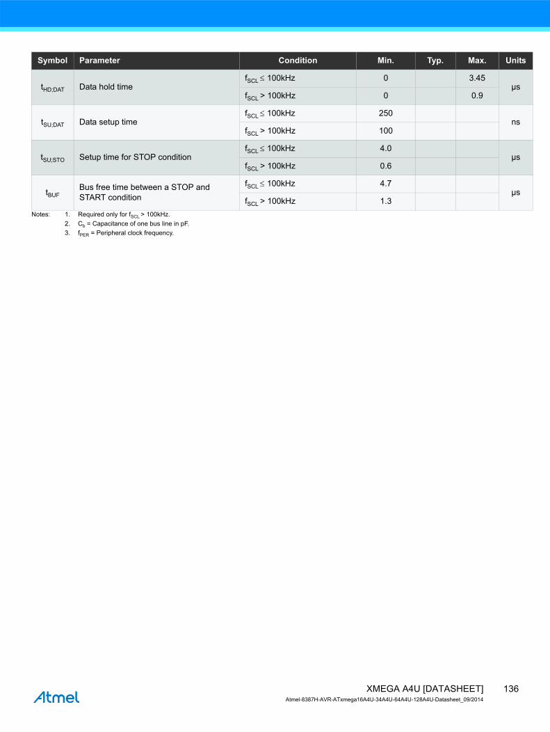
Notes: 1. Required only for fSCL > 100kHz.2. Cb = Capacitance of one bus line in pF.3. fPER = Peripheral clock frequency.
tHD;DAT Data hold timefSCL ≤ 100kHz 0 3.45
µsfSCL > 100kHz 0 0.9
tSU;DAT Data setup timefSCL ≤ 100kHz 250
nsfSCL > 100kHz 100
tSU;STO Setup time for STOP conditionfSCL ≤ 100kHz 4.0
µsfSCL > 100kHz 0.6
tBUFBus free time between a STOP and START condition
fSCL ≤ 100kHz 4.7µs
fSCL > 100kHz 1.3
Symbol Parameter Condition Min. Typ. Max. Units
136XMEGA A4U [DATASHEET]Atmel-8387H-AVR-ATxmega16A4U-34A4U-64A4U-128A4U-Datasheet_09/2014
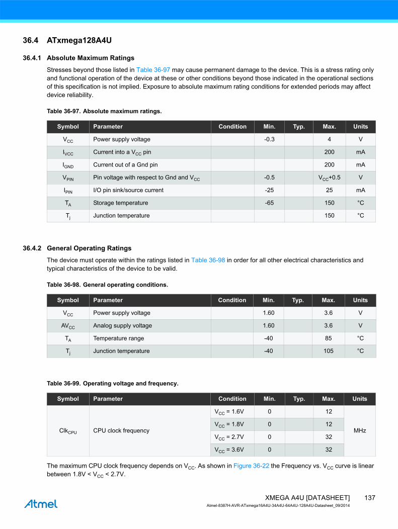
36.4 ATxmega128A4U
36.4.1 Absolute Maximum Ratings
Stresses beyond those listed in Table 36-97 may cause permanent damage to the device. This is a stress rating only and functional operation of the device at these or other conditions beyond those indicated in the operational sections of this specification is not implied. Exposure to absolute maximum rating conditions for extended periods may affect device reliability.
Table 36-97. Absolute maximum ratings.
36.4.2 General Operating Ratings
The device must operate within the ratings listed in Table 36-98 in order for all other electrical characteristics and typical characteristics of the device to be valid.
Table 36-98. General operating conditions.
Table 36-99. Operating voltage and frequency.
The maximum CPU clock frequency depends on VCC. As shown in Figure 36-22 the Frequency vs. VCC curve is linear between 1.8V < VCC < 2.7V.
Symbol Parameter Condition Min. Typ. Max. Units
VCC Power supply voltage -0.3 4 V
IVCC Current into a VCC pin 200 mA
IGND Current out of a Gnd pin 200 mA
VPIN Pin voltage with respect to Gnd and VCC -0.5 VCC+0.5 V
IPIN I/O pin sink/source current -25 25 mA
TA Storage temperature -65 150 °C
Tj Junction temperature 150 °C
Symbol Parameter Condition Min. Typ. Max. Units
VCC Power supply voltage 1.60 3.6 V
AVCC Analog supply voltage 1.60 3.6 V
TA Temperature range -40 85 °C
Tj Junction temperature -40 105 °C
Symbol Parameter Condition Min. Typ. Max. Units
ClkCPU CPU clock frequency
VCC = 1.6V 0 12
MHzVCC = 1.8V 0 12
VCC = 2.7V 0 32
VCC = 3.6V 0 32
137XMEGA A4U [DATASHEET]Atmel-8387H-AVR-ATxmega16A4U-34A4U-64A4U-128A4U-Datasheet_09/2014

Figure 36-22.Maximum Frequency vs. VCC.
1.8
12
32
MHz
V2.7 3.61.6
Safe Operating Area
138XMEGA A4U [DATASHEET]Atmel-8387H-AVR-ATxmega16A4U-34A4U-64A4U-128A4U-Datasheet_09/2014

36.4.3 Current consumption
Table 36-100.Current consumption for Active mode and sleep modes.
Notes: 1. All Power Reduction Registers set.2. Maximum limits are based on characterization, and not tested in production.
Symbol Parameter Condition Min. Typ. Max. Units
ICC
Active power consumption (1)
32kHz, Ext. ClkVCC = 1.8V 55
µA
VCC = 3.0V 135
1MHz, Ext. ClkVCC = 1.8V 255
VCC = 3.0V 535
2MHz, Ext. ClkVCC = 1.8V 460 600
VCC = 3.0V1.0 1.4
mA32MHz, Ext. Clk 9.5 12
Idle powerconsumption (1)
32kHz, Ext. ClkVCC = 1.8V 2.9
µA
VCC = 3.0V 3.9
1MHz, Ext. ClkVCC = 1.8V 62
VCC = 3.0V 118
2MHz, Ext. ClkVCC = 1.8V 125 225
VCC = 3.0V240 350
32MHz, Ext. Clk 3.8 5.5 mA
Power-down power consumption
T = 25°CVCC = 3.0V
0.1 1.0
µA
T = 85°C 1.5 4.5
T = 105°C 0.1 8.6
WDT and Sampled BOD enabled, T = 25°C
VCC = 3.0V
1.4 3.0
WDT and Sampled BOD enabled,T = 85°C 2.8 6.0
WDT and Sampled BOD enabled,T = 105°C 1.4 8.8
Power-save power consumption (2)
RTC from ULP clock, WDT and sampled BOD enabled, T = 25°C
VCC = 1.8V 1.2
µA
VCC = 3.0V 1.5
RTC from 1.024kHz low power 32.768kHz TOSC, T = 25°C
VCC = 1.8V 0.6 2.0
VCC = 3.0V 0.7 2.0
RTC from low power 32.768kHz TOSC, T = 25°C
VCC = 1.8V 0.8 3.0
VCC = 3.0V 1.0 3.0
Reset power consumption Current through RESET pin substracted VCC = 3.0V 300 µA
139XMEGA A4U [DATASHEET]Atmel-8387H-AVR-ATxmega16A4U-34A4U-64A4U-128A4U-Datasheet_09/2014

Table 36-101.Current consumption for modules and peripherals.
Note: 1. All parameters measured as the difference in current consumption between module enabled and disabled. All data at VCC = 3.0V, ClkSYS = 1MHz external clock without prescaling, T = 25°C unless other conditions are given.
Symbol Parameter Condition (1) Min. Typ. Max. Units
ICC
ULP oscillator 1.0 µA
32.768kHz int. oscillator 29 µA
2MHz int. oscillator85
µADFLL enabled with 32.768kHz int. osc. as reference 115
32MHz int. oscillator270
µADFLL enabled with 32.768kHz int. osc. as reference 440
PLL20x multiplication factor,
32MHz int. osc. DIV4 as reference320 µA
Watchdog timer 1.0 µA
BODContinuous mode 138
µASampled mode, includes ULP oscillator 1.2
Internal 1.0V reference 260 µA
Temperature sensor 250 µA
ADC 250kspsVREF = Ext ref
3.0 mA
CURRLIMIT = LOW 2.6
CURRLIMIT = MEDIUM 2.1
CURRLIMIT = HIGH 1.6
DAC250kspsVREF = Ext refNo load
Normal mode 1.9mA
Low power mode 1.1
ACHigh speed mode 330
µALow power mode 130
DMA 615kbps between I/O registers and SRAM 108 µA
Timer/counter 16 µA
USART Rx and Tx enabled, 9600 BAUD 2.5 µA
Flash memory and EEPROM programming 4.0 8.0 mA
140XMEGA A4U [DATASHEET]Atmel-8387H-AVR-ATxmega16A4U-34A4U-64A4U-128A4U-Datasheet_09/2014

36.4.4 Wake-up time from sleep modes
Table 36-102. Device wake-up time from sleep modes with various system clock sources.
Note: 1. The wake-up time is the time from the wake-up request is given until the peripheral clock is available on pin, see Figure 36-23. All peripherals and modules start execution from the first clock cycle, expect the CPU that is halted for four clock cycles before program execution starts.
Figure 36-23.Wake-up time definition.
Symbol Parameter Condition Min. Typ. (1) Max. Units
twakeup
Wake-up time from idle, standby, and extended standby mode
External 2MHz clock 2.0
µs32.768kHz internal oscillator 120
2MHz internal oscillator 2.0
32MHz internal oscillator 0.2
Wake-up time from power-save and power-down mode
External 2MHz clock 4.5
µs32.768kHz internal oscillator 320
2MHz internal oscillator 9.0
32MHz internal oscillator 5.0
Wakeup request
Clock output
Wakeup time
141XMEGA A4U [DATASHEET]Atmel-8387H-AVR-ATxmega16A4U-34A4U-64A4U-128A4U-Datasheet_09/2014

36.4.5 I/O Pin Characteristics
The I/O pins comply with the JEDEC LVTTL and LVCMOS specification and the high- and low level input and output voltage limits reflect or exceed this specification.
Table 36-103.I/O pin characteristics.
Notes: 1. The sum of all IOH for PORTA and PORTB must not exceed 100mA.The sum of all IOH for PORTC must not exceed 200mA.The sum of all IOH for PORTD and pins PE[0-1] on PORTE must not exceed 200mA.The sum of all IOH for PE[2-3] on PORTE, PORTR and PDI must not exceed 100mA.
2. The sum of all IOL for PORTA and PORTB must not exceed 100mA.The sum of all IOL for PORTC must not exceed 200mA.The sum of all IOL for PORTD and pins PE[0-1] on PORTE must not exceed 200mA.The sum of all IOL for PE[2-3] on PORTE, PORTR and PDI must not exceed 100mA.
Symbol Parameter Condition Min. Typ. Max. Units
IOH (1)/
IOL (2) I/O pin source/sink current -20 20 mA
VIH High level input voltage
VCC = 2.7 - 3.6V 2.0 VCC+0.3
VVCC = 2.0 - 2.7V 0.7*VCC VCC+0.3
VCC = 1.6 - 2.0V 0.8*VCC VCC+0.3
VIL Low level input voltage
VCC = 2.7- 3.6V -0.3 0.8
VVCC = 2.0 - 2.7V -0.3 0.3*VCC
VCC = 1.6 - 2.0V -0.3 0.2*VCC
VOH High level output voltage
VCC = 3.0 - 3.6V IOH = -2mA 2.4 0.94*VCC
V
VCC = 2.3 - 2.7VIOH = -1mA 2.0 0.96*VCC
IOH = -2mA 1.7 0.92*VCC
VCC = 3.3V IOH = -8mA 2.6 2.9
VCC = 3.0V IOH = -6mA 2.1 2.6
VCC = 1.8V IOH = -2mA 1.4 1.6
VOL Low level output voltage
VCC = 3.0 - 3.6V IOL = 2mA 0.05 0.4
V
VCC = 2.3 - 2.7VIOL = 1mA 0.03 0.4
IOL = 2mA 0.06 0.7
VCC = 3.3V IOL = 15mA 0.4 0.76
VCC = 3.0V IOL = 10mA 0.3 0.64
VCC = 1.8V IOL = 5mA 0.2 0.46
IIN Input leakage current T = 25°C <0.01 0.1 µA
RP Pull/buss keeper resistor 24 kΩ
tr Rise time No load4.0
nsslew rate limitation 7.0
142XMEGA A4U [DATASHEET]Atmel-8387H-AVR-ATxmega16A4U-34A4U-64A4U-128A4U-Datasheet_09/2014

36.4.6 ADC characteristics
Table 36-104.Power supply, reference and input range.
Table 36-105.Clock and timing.
Symbol Parameter Condition Min. Typ. Max. Units
AVCC Analog supply voltage VCC- 0.3 VCC+ 0.3 V
VREF Reference voltage 1 AVCC- 0.6 V
Rin Input resistance Switched 4.0 kΩ
Csample Input capacitance Switched 4.4 pF
RAREF Reference input resistance (leakage only) >10 MΩ
CAREF Reference input capacitance Static load 7 pF
VIN Input range -0.1 AVCC+0.1 V
Conversion range Differential mode, Vinp - Vinn -VREF VREF V
Conversion range Single ended unsigned mode, Vinp -ΔV VREF-ΔV V
∆V Fixed offset voltage 190 lsb
Symbol Parameter Condition Min. Typ. Max. Units
ClkADC ADC Clock frequency
Maximum is 1/4 of Peripheral clock frequency 100 2000
kHz
Measuring internal signals 100 125
fADC Sample rate
Current limitation (CURRLIMIT) off 100 2000
kspsCURRLIMIT = LOW 100 1500
CURRLIMIT = MEDIUM 100 1000
CURRLIMIT = HIGH 100 500
Sampling time 1/2 ClkADC cycle 0.25 5 µs
Conversion time (latency) (RES+2)/2+(GAIN !=0)RES (Resolution) = 8 or 12 5 8 ClkADC
cycles
Start-up time ADC clock cycles 12 24 ClkADCcycles
ADC settling timeAfter changing reference or input mode 7 7 ClkADC
cyclesAfter ADC flush 1 1
143XMEGA A4U [DATASHEET]Atmel-8387H-AVR-ATxmega16A4U-34A4U-64A4U-128A4U-Datasheet_09/2014

Table 36-106. Accuracy characteristics.
Notes: 1. Maximum numbers are based on characterisation and not tested in production, and valid for 5% to 95% input voltage range.2. Unless otherwise noted all linearity, offset and gain error numbers are valid under the condition that external VREF is used.
Table 36-107. Gain stage characteristics.
Symbol Parameter Condition (2) Min. Typ. Max. Units
RES Resolution Programmable to 8 or 12 bit 8 12 12 Bits
INL (1) Integral non-linearity
500kspsVCC-1.0V < VREF< VCC-0.6V ±1.2 ±2 lsb
All VREF ±1.5 ±3
2000kspsVCC-1.0V < VREF< VCC-0.6V ±1.0 ±2
All VREF ±1.5 ±3
DNL (1) Differential non-linearity guaranteed monotonic <±0.8 <±1 lsb
Offset error
-1.0 mV
Temperature drift <0.01 mV/K
Operating voltage drift <0.6 mV/V
Gain error
Differential mode
External reference -1
mVAVCC/1.6 10
AVCC/2.0 8.0
Bandgap ±5
Temperature drift <0.02 mV/K
Operating voltage drift <0.5 mV/V
Noise Differential mode, shorted input2msps, VCC = 3.6V, ClkPER = 16MHz 0.4 mV
rms
Symbol Parameter Condition Min. Typ. Max. Units
Rin Input resistance Switched in normal mode 4.0 kΩ
Csample Input capacitance Switched in normal mode 4.4 pF
Signal range Gain stage output 0 VCC- 0.6 V
Propagation delay ADC conversion rate 1.0 ClkADCcycles
Sample rate Same as ADC 100 1000 kHz
INL (1) Integral Non-Linearity 500ksps All gain settings ±1.5 ±4.0 lsb
Gain error
1x gain, normal mode -0.8
%8x gain, normal mode -2.5
64x gain, normal mode -3.5
144XMEGA A4U [DATASHEET]Atmel-8387H-AVR-ATxmega16A4U-34A4U-64A4U-128A4U-Datasheet_09/2014

s
Note: 1. Maximum numbers are based on characterisation and not tested in production, and valid for 5% to 95% input voltage range.
36.4.7 DAC Characteristics
Table 36-108. Power supply, reference and output range.
Table 36-109. Clock and timing.
Offset error,input referred
1x gain, normal mode -2.0
mV8x gain, normal mode -5.0
64x gain, normal mode -4.0
Noise
1x gain, normal modeVCC = 3.6V
Ext. VREF
0.5mV rms8x gain, normal mode 1.5
64x gain, normal mode 11
Symbol Parameter Condition Min. Typ. Max. Units
Symbol Parameter Condition Min. Typ. Max. Unit
AVCC Analog supply voltage VCC- 0.3 VCC+ 0.3
AVREF External reference voltage 1.0 VCC- 0.6 V
Rchannel DC output impedance 50 Ω
Linear output voltage range 0.15 AVCC-0.15 V
RAREF Reference input resistance >10 MΩ
CAREF Reference input capacitance Static load 7.0 pF
Minimum Resistance load 1 kΩ
Maximum capacitance load100 pF
1000Ω serial resistance 1 nF
Output sink/sourceOperating within accuracy specification AVCC/1000
mASafe operation 10
Symbol Parameter Condition Min. Typ. Max. Units
fDAC Conversion rate Cload=100pF, maximum step size
Normal mode 0 1000ksps
Low power mode 500
145XMEGA A4U [DATASHEET]Atmel-8387H-AVR-ATxmega16A4U-34A4U-64A4U-128A4U-Datasheet_09/2014

Table 36-110.Accuracy characteristics.
Note: 1. Maximum numbers are based on characterisation and not tested in production, and valid for 5% to 95% output voltage range.
Symbol Parameter Condition Min. Typ. Max. Units
RES Input resolution 12 Bits
INL (1) Integral non-linearity
VREF= Ext 1.0VVCC = 1.6V ±2.0 ±3.0
lsb
VCC = 3.6V ±1.5 ±2.5
VREF=AVCC
VCC = 1.6V ±2.0 ±4.0
VCC = 3.6V ±1.5 ±4.0
VREF=INT1VVCC = 1.6V ±5.0
VCC = 3.6V ±5.0
DNL (1) Differential non-linearity
VREF=Ext 1.0VVCC = 1.6V ±1.5 3.0
lsb
VCC = 3.6V ±0.6 1.5
VREF=AVCC
VCC = 1.6V ±1.0 3.5
VCC = 3.6V ±0.6 1.5
VREF=INT1VVCC = 1.6V ±4.5
VCC = 3.6V ±4.5
Gain error After calibration <4.0 lsb
Gain calibration step size 4.0 lsb
Gain calibration drift VREF= Ext 1.0V <0.2 mV/K
Offset error After calibration <1.0 lsb
Offset calibration step size 1.0
146XMEGA A4U [DATASHEET]Atmel-8387H-AVR-ATxmega16A4U-34A4U-64A4U-128A4U-Datasheet_09/2014

36.4.8 Analog Comparator Characteristics
Table 36-111. Analog Comparator characteristics.
36.4.9 Bandgap and Internal 1.0V Reference Characteristics
Table 36-112. Bandgap and Internal 1.0V reference characteristics.
Symbol Parameter Condition Min. Typ. Max. Units
Voff Input offset voltage <±10 mV
Ilk Input leakage current <1 nA
Input voltage range -0.1 AVCC V
AC startup time 100 µs
Vhys1 Hysteresis, none 0 mV
Vhys2 Hysteresis, smallmode = High Speed (HS) 13
mVmode = Low Power (LP) 30
Vhys3 Hysteresis, largemode = HS 30
mVmode = LP 60
tdelay Propagation delay
VCC = 3.0V, T= 85°C mode = HS 30 90
nsmode = HS 30
VCC = 3.0V, T= 85°C mode = LP 130 500
mode = LP 130
64-level voltage scaler Integral non-linearity (INL) 0.3 0.5 lsb
Symbol Parameter Condition Min. Typ. Max. Units
Startup timeAs reference for ADC or DAC 1 ClkPER + 2.5µs
µsAs input voltage to ADC and AC 1.5
Bandgap voltage 1.1 V
INT1V Internal 1.00V reference T= 85°C, after calibration 0.99 1.0 1.01 V
Variation over voltage and temperature Relative to T= 85°C, VCC = 3.0V ±1.5 %
147XMEGA A4U [DATASHEET]Atmel-8387H-AVR-ATxmega16A4U-34A4U-64A4U-128A4U-Datasheet_09/2014

36.4.10 Brownout Detection Characteristics
Table 36-113. Brownout detection characteristics.
36.4.11 External Reset Characteristics
Table 36-114. External reset characteristics.
36.4.12 Power-on Reset Characteristics
Table 36-115. Power-on reset characteristics.
Note: 1. VPOT- values are only valid when BOD is disabled. When BOD is enabled VPOT- = VPOT+.
Symbol Parameter Condition Min. Typ. Max. Units
VBOT
BOD level 0 falling VCC 1.50 1.62 1.72
V
BOD level 1 falling VCC 1.8
BOD level 2 falling VCC 2.0
BOD level 3 falling VCC 2.2
BOD level 4 falling VCC 2.4
BOD level 5 falling VCC 2.6
BOD level 6 falling VCC 2.8
BOD level 7 falling VCC 3.0
tBOD Detection timeContinuous mode 0.4
µsSampled mode 1000
VHYST Hysteresis 1.2 %
Symbol Parameter Condition Min. Typ. Max. Units
tEXT Minimum reset pulse width 1000 95 ns
VRST
Reset threshold voltage (VIH)VCC = 2.7 - 3.6V 0.60×VCC
VVCC = 1.6 - 2.7V 0.60×VCC
Reset threshold voltage (VIL)VCC = 2.7 - 3.6V 0.50×VCC
VCC = 1.6 - 2.7V 0.40×VCC
RRST Reset pin Pull-up Resistor 25 kΩ
Symbol Parameter Condition Min. Typ. Max. Units
VPOT- (1) POR threshold voltage falling VCC
VCC falls faster than 1V/ms 0.4 1.0V
VCC falls at 1V/ms or slower 0.8 1.0
VPOT+ POR threshold voltage rising VCC 1.3 1.59 mV
148XMEGA A4U [DATASHEET]Atmel-8387H-AVR-ATxmega16A4U-34A4U-64A4U-128A4U-Datasheet_09/2014

36.4.13 Flash and EEPROM Memory Characteristics
Table 36-116. Endurance and data retention.
Table 36-117. Programming time.
Notes: 1. Programming is timed from the 2MHz internal oscillator.2. EEPROM is not erased if the EESAVE fuse is programmed.
Symbol Parameter Condition Min. Typ. Max. Units
Flash
Write/Erase cycles
25°C 10K
Cycle85°C 10K
105°C 2K
Data retention
25°C 100
Year85°C 25
105°C 10
EEPROM
Write/Erase cycles
25°C 100K
Cycle85°C 100K
105°C 30K
Data retention
25°C 100
Year85°C 25
105°C 10
Symbol Parameter Condition Min. Typ.(1) Max. Units
Chip Erase 128KB Flash, EEPROM(2) and SRAM Erase 75 ms
Application Erase Section erase 6 ms
Flash
Page erase 4
msPage write 4
Atomic page erase and write 8
EEPROM
Page erase 4
msPage write 4
Atomic page erase and write 8
149XMEGA A4U [DATASHEET]Atmel-8387H-AVR-ATxmega16A4U-34A4U-64A4U-128A4U-Datasheet_09/2014

36.4.14 Clock and Oscillator Characteristics
36.4.14.1 Calibrated 32.768kHz Internal Oscillator characteristics
Table 36-118. 32.768kHz internal oscillator characteristics.
36.4.14.2 Calibrated 2MHz RC Internal Oscillator characteristics
Table 36-119. 2MHz internal oscillator characteristics.
36.4.14.3 Calibrated and tunable 32MHz internal oscillator characteristics
Table 36-120. 32MHz internal oscillator characteristics.
36.4.14.4 32kHz Internal ULP Oscillator characteristics
Table 36-121. 32kHz internal ULP oscillator characteristics.
Symbol Parameter Condition Min. Typ. Max. Units
Frequency 32.768 kHz
Factory calibration accuracy T = 85°C, VCC = 3.0V -0.5 0.5 %
User calibration accuracy -0.5 0.5 %
Symbol Parameter Condition Min. Typ. Max. Units
Frequency range DFLL can tune to this frequency over voltage and temperature 1.8 2.2 MHz
Factory calibrated frequency 2.0 MHz
Factory calibration accuracy T = 85°C, VCC= 3.0V -1.5 1.5 %
User calibration accuracy -0.2 0.2 %
DFLL calibration stepsize 0.21 %
Symbol Parameter Condition Min. Typ. Max. Units
Frequency range DFLL can tune to this frequency over voltage and temperature 30 55 MHz
Factory calibrated frequency 32 MHz
Factory calibration accuracy T = 85°C, VCC= 3.0V -1.5 1.5 %
User calibration accuracy -0.2 0.2 %
DFLL calibration step size 0.22 %
Symbol Parameter Condition Min. Typ. Max. Units
Output frequency 32 kHz
Accuracy -30 30 %
150XMEGA A4U [DATASHEET]Atmel-8387H-AVR-ATxmega16A4U-34A4U-64A4U-128A4U-Datasheet_09/2014

36.4.14.5 Internal Phase Locked Loop (PLL) characteristics
Table 36-122. Internal PLL characteristics.
Note: 1. The maximum output frequency vs. supply voltage is linear between 1.8V and 2.7V, and can never be higher than four times the maximum CPU frequency.
36.4.14.6 External clock characteristics
Figure 36-24. External clock drive waveform
Table 36-123.External clock used as system clock without prescaling.
Note: 1. The maximum frequency vs. supply voltage is linear between 1.6V and 2.7V, and the same applies for all other parameters with supply voltage conditions.
Symbol Parameter Condition Min. Typ. Max. Units
fIN Input frequency Output frequency must be within fOUT 0.4 64 MHz
fOUT Output frequency (1)VCC= 1.6 - 1.8V 20 48
MHzVCC= 2.7 - 3.6V 20 128
Start-up time 25 µs
Re-lock time 25 µs
tCH
tCL
tCK
tCH
VIL1
VIH1
tCR tCF
Symbol Parameter Condition Min. Typ. Max. Units
1/tCK Clock Frequency (1)VCC = 1.6 - 1.8V 0 12
MHzVCC = 2.7 - 3.6V 0 32
tCK Clock PeriodVCC = 1.6 - 1.8V 83.3
nsVCC = 2.7 - 3.6V 31.5
tCH Clock High TimeVCC = 1.6 - 1.8V 30.0
nsVCC = 2.7 - 3.6V 12.5
tCL Clock Low TimeVCC = 1.6 - 1.8V 30.0
nsVCC = 2.7 - 3.6V 12.5
tCR Rise Time (for maximum frequency)VCC = 1.6 - 1.8V 10
nsVCC = 2.7 - 3.6V 3
tCF Fall Time (for maximum frequency)VCC = 1.6 - 1.8V 10
nsVCC = 2.7 - 3.6V 3
ΔtCK Change in period from one clock cycle to the next 10 %
151XMEGA A4U [DATASHEET]Atmel-8387H-AVR-ATxmega16A4U-34A4U-64A4U-128A4U-Datasheet_09/2014

Table 36-124. External clock with prescaler (1)for system clock.
Notes: 1. System Clock Prescalers must be set so that maximum CPU clock frequency for device is not exceeded.2. The maximum frequency vs. supply voltage is linear between 1.6V and 2.7V, and the same applies for all other parameters with supply voltage conditions.
36.4.14.7 External 16MHz crystal oscillator and XOSC characteristic
Table 36-125. External 16MHz crystal oscillator and XOSC characteristics.
Symbol Parameter Condition Min. Typ. Max. Units
1/tCK Clock Frequency (2)VCC = 1.6 - 1.8V 0 90
MHzVCC = 2.7 - 3.6V 0 142
tCK Clock PeriodVCC = 1.6 - 1.8V 11
nsVCC = 2.7 - 3.6V 7
tCH Clock High TimeVCC = 1.6 - 1.8V 4.5
nsVCC = 2.7 - 3.6V 2.4
tCL Clock Low TimeVCC = 1.6 - 1.8V 4.5
nsVCC = 2.7 - 3.6V 2.4
tCR Rise Time (for maximum frequency)VCC = 1.6 - 1.8V 1.5
nsVCC = 2.7 - 3.6V 1.0
tCF Fall Time (for maximum frequency)VCC = 1.6 - 1.8V 1.5
nsVCC = 2.7 - 3.6V 1.0
ΔtCK Change in period from one clock cycle to the next 10 %
Symbol Parameter Condition Min. Typ. Max. Units
Cycle to cycle jitterXOSCPWR=0
FRQRANGE=0 <10
nsFRQRANGE=1, 2, or 3 <1
XOSCPWR=1 <1
Long term jitterXOSCPWR=0
FRQRANGE=0 <6
nsFRQRANGE=1, 2, or 3 <0.5
XOSCPWR=1 <0.5
Frequency errorXOSCPWR=0
FRQRANGE=0 <0.1
%FRQRANGE=1 <0.05
FRQRANGE=2 or 3 <0.005
XOSCPWR=1 <0.005
152XMEGA A4U [DATASHEET]Atmel-8387H-AVR-ATxmega16A4U-34A4U-64A4U-128A4U-Datasheet_09/2014

Note: 1. Numbers for negative impedance are not tested in production but guaranteed from design and characterization.
Duty cycleXOSCPWR=0
FRQRANGE=0 40
%FRQRANGE=1 42
FRQRANGE=2 or 3 45
XOSCPWR=1 48
RQ Negative impedance (1)
XOSCPWR=0,FRQRANGE=0
0.4MHz resonator, CL=100pF 2.4k
Ω
1MHz crystal, CL=20pF 8.7k
2MHz crystal, CL=20pF 2.1k
XOSCPWR=0,FRQRANGE=1,CL=20pF
2MHz crystal 4.2k
8MHz crystal 250
9MHz crystal 195
XOSCPWR=0,FRQRANGE=2,CL=20pF
8MHz crystal 360
9MHz crystal 285
12MHz crystal 155
XOSCPWR=0,FRQRANGE=3,CL=20pF
9MHz crystal 365
12MHz crystal 200
16MHz crystal 105
XOSCPWR=1,FRQRANGE=0,CL=20pF
9MHz crystal 435
12MHz crystal 235
16MHz crystal 125
XOSCPWR=1,FRQRANGE=1,CL=20pF
9MHz crystal 495
12MHz crystal 270
16MHz crystal 145
XOSCPWR=1,FRQRANGE=2,CL=20pF
12MHz crystal 305
16MHz crystal 160
XOSCPWR=1,FRQRANGE=3,CL=20pF
12MHz crystal 380
16MHz crystal 205
ESR SF = Safety factor min(RQ)/SF kΩ
CXTAL1Parasitic capacitance XTAL1 pin 5.45 pF
CXTAL2Parasitic capacitance XTAL2 pin 7.51 pF
CLOADParasitic capacitance load 3.16 pF
Symbol Parameter Condition Min. Typ. Max. Units
153XMEGA A4U [DATASHEET]Atmel-8387H-AVR-ATxmega16A4U-34A4U-64A4U-128A4U-Datasheet_09/2014

36.4.14.8 External 32.768kHz crystal oscillator and TOSC characteristics
Table 36-126. External 32.768kHz crystal oscillator and TOSC characteristics.
Note: 1. See Figure 36-25 for definition.
Figure 36-25. TOSC input capacitance.
The parasitic capacitance between the TOSC pins is CL1 + CL2 in series as seen from the crystal when oscillating without external capacitors.
Symbol Parameter Condition Min. Typ. Max. Units
ESR/R1 Recommended crystal equivalent series resistance (ESR)
Crystal load capacitance 6.5pF 60kΩ
Crystal load capacitance 9.0pF 35
CTOSC1 Parasitic capacitance TOSC1 pin5.4
pFAlternate TOSC location 4.0
CTOSC2 Parasitic capacitance TOSC2 pin7.1
pFAlternate TOSC location 4.0
Recommended safety factor capacitance load matched to crystal specification 3
CL1 CL2
2CSOT1CSOT Device internalExternal
32.768kHz crystal
154XMEGA A4U [DATASHEET]Atmel-8387H-AVR-ATxmega16A4U-34A4U-64A4U-128A4U-Datasheet_09/2014

36.4.15 SPI Characteristics
Figure 36-26. SPI timing requirements in master mode.
Figure 36-27. SPI timing requirements in slave mode.
MSB LSB
MSB LSB
tMOS
tMIS tMIH
tSCKW
tSCK
tMOH tMOH
tSCKFtSCKR
tSCKW
MOSI(Data output)
MISO(Data input)
SCK(CPOL = 1)
SCK(CPOL = 0)
SS
MSB LSB
MSB LSB
tSIS tSIH
tSSCKW
tSSCKW
tSSCK
tSSH
tSOSSH
tSCKR tSCKF
tSOS
tSSS
tSOSSS
MISO(Data output)
MOSI(Data input)
SCK(CPOL = 1)
SCK(CPOL = 0)
SS
155XMEGA A4U [DATASHEET]Atmel-8387H-AVR-ATxmega16A4U-34A4U-64A4U-128A4U-Datasheet_09/2014

Table 36-127. SPI timing characteristics and requirements.
Symbol Parameter Condition Min. Typ. Max. Units
tSCK SCK Period Master (See Table 21-4 in XMEGA AU Manual)
ns
tSCKW SCK high/low width Master 0.5×SCK
tSCKR SCK Rise time Master 2.7
tSCKF SCK Fall time Master 2.7
tMIS MISO setup to SCK Master 10
tMIH MISO hold after SCK Master 10
tMOS MOSI setup SCK Master 0.5×SCK
tMOH MOSI hold after SCK Master 1
tSSCK Slave SCK Period Slave 4×t ClkPER
tSSCKW SCK high/low width Slave 2×t ClkPER
tSSCKR SCK Rise time Slave 1600
tSSCKF SCK Fall time Slave 1600
tSIS MOSI setup to SCK Slave 3
tSIH MOSI hold after SCK Slave t ClkPER
tSSS SS setup to SCK Slave 21
tSSH SS hold after SCK Slave 20
tSOS MISO setup SCK Slave 8
tSOH MISO hold after SCK Slave 13
tSOSS MISO setup after SS low Slave 11
tSOSH MISO hold after SS high Slave 8
156XMEGA A4U [DATASHEET]Atmel-8387H-AVR-ATxmega16A4U-34A4U-64A4U-128A4U-Datasheet_09/2014

36.4.16 Two-Wire Interface Characteristics
Table 36-128 describes the requirements for devices connected to the Two-Wire Interface Bus. The Atmel AVR XMEGA Two-Wire Interface meets or exceeds these requirements under the noted conditions. Timing symbols refer to Figure 36-28.
Figure 36-28. Two-wire interface bus timing.
Table 36-128. Two-wire interface characteristics.
tHD;STA
tof
SDA
SCL
tLOWtHIGH
tSU;STA
tBUF
tr
tHD;DAT tSU;DATtSU;STO
Symbol Parameter Condition Min. Typ. Max. Units
VIH Input High Voltage 0.7VCC VCC+0.5 V
VIL Input Low Voltage 0.5 0.3×VCC V
Vhys Hysteresis of Schmitt Trigger Inputs 0.05VCC (1) V
VOL Output Low Voltage 3mA, sink current 0 0.4 V
tr Rise Time for both SDA and SCL 20+0.1Cb (1)(2) 300 ns
tof Output Fall Time from VIHmin to VILmax 10pF < Cb < 400pF (2) 20+0.1Cb (1)(2) 250 ns
tSP Spikes Suppressed by Input Filter 0 50 ns
II Input Current for each I/O Pin 0.1VCC < VI < 0.9VCC -10 10 µA
CI Capacitance for each I/O Pin 10 pF
fSCL SCL Clock Frequency fPER (3)>max(10fSCL, 250kHz) 0 400 kHz
RP Value of Pull-up resistor
fSCL ≤ 100kHz
ΩfSCL > 100kHz
tHD;STA Hold Time (repeated) START conditionfSCL ≤ 100kHz 4.0
µsfSCL > 100kHz 0.6
tLOW Low Period of SCL ClockfSCL ≤ 100kHz 4.7
µsfSCL > 100kHz 1.3
tHIGH High Period of SCL ClockfSCL ≤ 100kHz 4.0
µsfSCL > 100kHz 0.6
tSU;STASet-up time for a repeated START condition
fSCL ≤ 100kHz 4.7µs
fSCL > 100kHz 0.6
VCC 0.4V–3mA
----------------------------
100nsCb---------------
300nsCb---------------
157XMEGA A4U [DATASHEET]Atmel-8387H-AVR-ATxmega16A4U-34A4U-64A4U-128A4U-Datasheet_09/2014

Notes: 1. Required only for fSCL > 100kHz.2. Cb = Capacitance of one bus line in pF.3. fPER = Peripheral clock frequency.
tHD;DAT Data hold timefSCL ≤ 100kHz 0 3.45
µsfSCL > 100kHz 0 0.9
tSU;DAT Data setup timefSCL ≤ 100kHz 250
nsfSCL > 100kHz 100
tSU;STO Setup time for STOP conditionfSCL ≤ 100kHz 4.0
µsfSCL > 100kHz 0.6
tBUFBus free time between a STOP and START condition
fSCL ≤ 100kHz 4.7µs
fSCL > 100kHz 1.3
Symbol Parameter Condition Min. Typ. Max. Units
158XMEGA A4U [DATASHEET]Atmel-8387H-AVR-ATxmega16A4U-34A4U-64A4U-128A4U-Datasheet_09/2014

37. Typical Characteristics
37.1 ATxmega16A4U
37.1.1 Current consumption
37.1.1.1 Active mode supply current
Figure 37-1. Active supply current vs. frequency.fSYS = 0 - 1MHz external clock, T = 25°C.
Figure 37-2. Active supply current vs. frequency.fSYS = 1 - 32MHz external clock, T = 25°C.
3.3V
3.0V
2.7V
2.2V
1.8V
0
60
120
180
240
300
360
420
480
540
600
0 0.1 0.2 0.3 0.4 0.5 0.6 0.7 0.8 0.9 1
Frequency [MHz]
ICC [µ
A]
3.3V
3.0V
2.7V
0
2
4
6
8
10
12
0 4 8 12 16 20 24 28 32
Frequency [MHz]
I CC [m
A]
2.2V
1.8V
159XMEGA A4U [DATASHEET]Atmel-8387H-AVR-ATxmega16A4U-34A4U-64A4U-128A4U-Datasheet_09/2014

Figure 37-3. Active mode supply current vs. VCC.fSYS = 32.768kHz internal oscillator.
Figure 37-4. Active mode supply current vs. VCC.fSYS = 1MHz external clock.
105 °C85 °C
25 °C
-40 °C
70
90
110
130
150
170
190
210
230
250
270
1.6 1.8 2 2.2 2.4 2.6 2.8 3 3.2 3.4 3.6
I CC
[uA
]
VCC [V]
105 °C85 °C25 °C-40 °C
200
300
400
500
600
700
800
1.6 1.8 2 2.2 2.4 2.6 2.8 3 3.2 3.4 3.6
I CC
[uA
]
VCC [V]
160XMEGA A4U [DATASHEET]Atmel-8387H-AVR-ATxmega16A4U-34A4U-64A4U-128A4U-Datasheet_09/2014

Figure 37-5. Active mode supply current vs. VCC.fSYS = 2MHz internal oscillator.
Figure 37-6. Active mode supply current vs. VCC.fSYS = 32MHz internal oscillator prescaled to 8MHz.
105 °C85 °C25 °C-40 °C
400
600
800
1000
1200
1400
1600
1.6 1.8 2 2.2 2.4 2.6 2.8 3 3.2 3.4 3.6
I CC
[uA
]
VCC [V]
105 °C85 °C25 °C-40 °C
1400
1900
2400
2900
3400
3900
4400
4900
5400
5900
1.6 1.8 2 2.2 2.4 2.6 2.8 3 3.2 3.4 3.6
I CC
[uA
]
VCC [V]
161XMEGA A4U [DATASHEET]Atmel-8387H-AVR-ATxmega16A4U-34A4U-64A4U-128A4U-Datasheet_09/2014

Figure 37-7. Active mode supply current vs. VCC.fSYS = 32MHz internal oscillator.
37.1.1.2 Idle mode supply current
Figure 37-8. Idle mode supply current vs. frequency.fSYS = 0 - 1MHz external clock, T = 25°C.
105 °C85 °C
25 °C
-40 °C
3400
3625
3850
4075
4300
4525
4750
4975
5200
5425
5650
2.7 2.8 2.9 3 3.1 3.2 3.3 3.4 3.5 3.6
I CC
[uA
]
VCC [V]
3.3V
3.0V
2.7V
2.2V
1.8V
0
20
40
60
80
100
120
140
0 0.1 0.2 0.3 0.4 0.5 0.6 0.7 0.8 0.9 1.0
Frequency [MHz]
I CC [µ
A]
162XMEGA A4U [DATASHEET]Atmel-8387H-AVR-ATxmega16A4U-34A4U-64A4U-128A4U-Datasheet_09/2014

Figure 37-9. Idle mode supply current vs. frequency.fSYS = 1 - 32MHz external clock, T = 25°C.
Figure 37-10. Idle mode supply current vs. VCC.fSYS = 32.768kHz internal oscillator.
3.3V
3.0V
2.7V
0
0.5
1.0
1.5
2.0
2.5
3.0
3.5
4.0
4.5
0 4 8 12 16 20 24 28 32
Frequency [MHz]
I CC [m
A]
2.2V
1.8V
105 °C
85 °C25 °C
-40 °C
27
28
29
30
31
32
33
34
35
1.6 1.8 2 2.2 2.4 2.6 2.8 3 3.2 3.4 3.6
I CC
[uA
]
VCC [V]
163XMEGA A4U [DATASHEET]Atmel-8387H-AVR-ATxmega16A4U-34A4U-64A4U-128A4U-Datasheet_09/2014
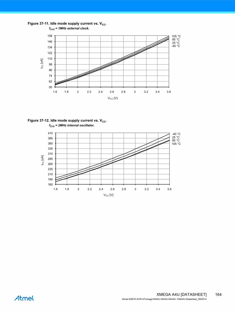
Figure 37-11. Idle mode supply current vs. VCC.fSYS = 1MHz external clock.
Figure 37-12. Idle mode supply current vs. VCC.fSYS = 2MHz internal oscillator.
105 °C85 °C25 °C-40 °C
50
62
74
86
98
110
122
134
146
158
1.6 1.8 2 2.2 2.4 2.6 2.8 3 3.2 3.4 3.6
I CC
[uA
]
VCC [V]
105 °C85 °C25 °C-40 °C
160
185
210
235
260
285
310
335
360
385
410
1.6 1.8 2 2.2 2.4 2.6 2.8 3 3.2 3.4 3.6
I CC
[uA
]
VCC [V]
164XMEGA A4U [DATASHEET]Atmel-8387H-AVR-ATxmega16A4U-34A4U-64A4U-128A4U-Datasheet_09/2014

Figure 37-13. Idle mode supply current vs. VCC.fSYS = 32MHz internal oscillator prescaled to 8MHz.
Figure 37-14. Idle mode current vs. VCC.fSYS = 32MHz internal oscillator.
105 °C85 °C25 °C-40 °C
600
800
1000
1200
1400
1600
1800
2000
1.6 1.8 2 2.2 2.4 2.6 2.8 3 3.2 3.4 3.6
I CC
[uA
]
VCC [V]
105 °C85 °C
25 °C
-40 °C
3400
3625
3850
4075
4300
4525
4750
4975
5200
5425
5650
2.7 2.8 2.9 3 3.1 3.2 3.3 3.4 3.5 3.6
I CC
[uA
]
VCC [V]
165XMEGA A4U [DATASHEET]Atmel-8387H-AVR-ATxmega16A4U-34A4U-64A4U-128A4U-Datasheet_09/2014

37.1.1.3 Power-down mode supply current
Figure 37-15. Power-down mode supply current vs. temperature.All functions disabled.
Figure 37-16. Power-down mode supply current vs. VCC.All functions disabled.
3.6 V
3.0 V2.7 V2.2 V1.8 V1.6 V
0.00
0.50
1.00
1.50
2.00
2.50
3.00
3.50
-40 -25 -10 5 20 35 50 65 80 95 110
I CC
[uA
]
Temperature [°C]
105 °C
85 °C
25 °C-40 °C0.0
0.4
0.8
1.2
1.6
2.0
2.4
2.8
3.2
3.6
1.6 1.8 2 2.2 2.4 2.6 2.8 3 3.2 3.4 3.6
ICC
[uA
]
VCC [V]
166XMEGA A4U [DATASHEET]Atmel-8387H-AVR-ATxmega16A4U-34A4U-64A4U-128A4U-Datasheet_09/2014

Figure 37-17. Power-down mode supply current vs. VCC.Watchdog and sampled BOD enabled.
37.1.1.4 Power-save mode supply current
Figure 37-18. Power-save mode supply current vs.VCC.Real Time Counter enabled and running from 1.024kHz output of 32.768kHz TOSC.
105 °C
85 °C
25 °C-40 °C
1.1
1.6
2.1
2.6
3.1
3.6
4.1
4.6
5.1
1.6 1.8 2.0 2.2 2.4 2.6 2.8 3.0 3.2 3.4 3.6
I CC
[µA
]
VCC [V]
Normal mode
Low-power mode
0
0.1
0.2
0.3
0.4
0.5
0.6
0.7
0.8
0.9
VCC [V]
I CC
[µA
]
1.6 1.8 2.0 2.2 2.4 2.6 2.8 3.0 3.2 3.4 3.6
167XMEGA A4U [DATASHEET]Atmel-8387H-AVR-ATxmega16A4U-34A4U-64A4U-128A4U-Datasheet_09/2014

37.1.1.5 Standby mode supply current
Figure 37-19. Standby supply current vs. VCC.Standby, fSYS = 1MHz.
Figure 37-20. Standby supply current vs. VCC.25°C, running from different crystal oscillators.
105 °C
85 °C
25 °C-40 °C
2.5
3.5
4.5
5.5
6.5
7.5
8.5
9.5
10.5
11.5
12.5
1.6 1.8 2 2.2 2.4 2.6 2.8 3 3.2 3.4 3.6
I CC
[uA
]
VCC [V]
16MHz12MHz
8MHz
2MHz
0.454MHz
160
200
240
280
320
360
400
440
480
1.6 1.8 2 2.2 2.4 2.6 2.8 3 3.2 3.4 3.6
VCC [V]
ICC
[µA
]
168XMEGA A4U [DATASHEET]Atmel-8387H-AVR-ATxmega16A4U-34A4U-64A4U-128A4U-Datasheet_09/2014

37.1.2 I/O Pin Characteristics
37.1.2.1 Pull-up
Figure 37-21. I/O pin pull-up resistor current vs. input voltage.VCC = 1.8V.
Figure 37-22. I/O pin pull-up resistor current vs. input voltage.VCC = 3.0V.
105 °C85 °C25 °C
-40 °C
0
8
16
24
32
40
48
56
64
72
0.0 0.2 0.4 0.6 0.8 1.0 1.2 1.4 1.6 1.8
I [µA
]
VPIN [V]
105 °C85 °C25 °C
-40 °C
0
15
30
45
60
75
90
105
120
0.0 0.3 0.6 0.9 1.2 1.5 1.8 2.1 2.4 2.7 3.0
I [µA
]
VPIN [V]
169XMEGA A4U [DATASHEET]Atmel-8387H-AVR-ATxmega16A4U-34A4U-64A4U-128A4U-Datasheet_09/2014

Figure 37-23. I/O pin pull-up resistor current vs. input voltage.VCC = 3.3V.
37.1.2.2 Output Voltage vs. Sink/Source Current
Figure 37-24. I/O pin output voltage vs. source current.VCC = 1.8V.
105 °C85 °C25 °C
-40 °C
0
15
30
45
60
75
90
105
120
135
0.0 0.3 0.6 0.9 1.2 1.5 1.8 2.1 2.4 2.7 3.0 3.3
I [µA
]
VPIN [V]
105 °C85 °C
25 °C-40 °C
0.0
0.2
0.4
0.6
0.8
1.0
1.2
1.4
1.6
1.8
-10 -9 -8 -7 -6 -5 -4 -3 -2 -1 0
VP
IN[V
]
IPIN [mA]
170XMEGA A4U [DATASHEET]Atmel-8387H-AVR-ATxmega16A4U-34A4U-64A4U-128A4U-Datasheet_09/2014

Figure 37-25. I/O pin output voltage vs. source current.VCC = 3.0V.
Figure 37-26. I/O pin output voltage vs. source current.VCC = 3.3V.
105 °C85 °C25 °C
-40 °C
0.0
0.3
0.6
0.9
1.2
1.5
1.8
2.1
2.4
2.7
3.0
-32 -28 -24 -20 -16 -12 -8 -4 0
VP
IN[V
]
IPIN [mA]
105 °C85 °C
25 °C
-40 °C
0.00.30.60.91.21.51.82.12.42.73.03.3
-32 -28 -24 -20 -16 -12 -8 -4 0
VP
IN[V
]
IPIN [mA]
171XMEGA A4U [DATASHEET]Atmel-8387H-AVR-ATxmega16A4U-34A4U-64A4U-128A4U-Datasheet_09/2014

Figure 37-27. I/O pin output voltage vs. source current.
Figure 37-28. I/O pin output voltage vs. sink current.VCC = 1.8V.
3.6V
3.3V
3.0V
2.7V
2.3V
1.8V
0.5
1.0
1.5
2.0
2.5
3.0
3.5
4.0
-24 -21 -18 -15 -12 -9 -6 -3 0
IPIN [mA]
VP
IN [V
]
105 °C85 °C
25 °C
-40 °C
0.0
0.1
0.2
0.3
0.4
0.5
0.6
0.7
0.8
0.9
1.0
0 2 4 6 8 10 12 14 16
VP
IN[V
]
IPIN [mA]
172XMEGA A4U [DATASHEET]Atmel-8387H-AVR-ATxmega16A4U-34A4U-64A4U-128A4U-Datasheet_09/2014

Figure 37-29. I/O pin output voltage vs. sink current.VCC = 3.0V.
Figure 37-30. I/O pin output voltage vs. sink current.VCC = 3.3V.
Figure 37-31. I/O pin output voltage vs. sink current.
105 °C85 °C25 °C-40 °C
0.0
0.1
0.2
0.3
0.4
0.5
0.6
0.7
0 2 4 6 8 10 12 14 16 18 20
VP
IN[V
]
IPIN [mA]
105 °C85 °C
25 °C-40 °C
0.0
0.1
0.2
0.3
0.4
0.5
0.6
0.7
0.8
0.9
1.0
0 4 8 12 16 20 24 28 32
VP
IN[V
]
IPIN [mA]
0
0.3
0.6
0.9
1.2
1.5
0 5 10 15 20 25 30
IPIN [mA]
VP
IN [
V]
1.8V
3.6V3.3V3.0V2.7V
2.3V
173XMEGA A4U [DATASHEET]Atmel-8387H-AVR-ATxmega16A4U-34A4U-64A4U-128A4U-Datasheet_09/2014

37.1.2.3 Thresholds and Hysteresis
Figure 37-32. I/O pin input threshold voltage vs. VCC.T = 25°C.
Figure 37-33. I/O pin input threshold voltage vs. VCC.VIH I/O pin read as “1”.
VIL
VIH
0.0
0.2
0.4
0.6
0.8
1.0
1.2
1.4
1.6
1.8
1.6 1.8 2 2.2 2.4 2.6 2.8 3 3.2 3.4 3.6
Vcc [V]
Vth
reshold
[V
]
105 °C85 °C25 °C
-40 °C
0.8
0.9
1.0
1.1
1.2
1.3
1.4
1.5
1.6
1.7
1.8
1.6 1.8 2.0 2.2 2.4 2.6 2.8 3.0 3.2 3.4 3.6
Vth
resh
old
[V]
VCC [V]
174XMEGA A4U [DATASHEET]Atmel-8387H-AVR-ATxmega16A4U-34A4U-64A4U-128A4U-Datasheet_09/2014

Figure 37-34. I/O pin input threshold voltage vs. VCC.VIL I/O pin read as “0”.
Figure 37-35. I/O pin input hysteresis vs. VCC.
105 °C85 °C25 °C
-40 °C
0.55
0.70
0.85
1.00
1.15
1.30
1.45
1.60
1.75
1.6 1.8 2.0 2.2 2.4 2.6 2.8 3.0 3.2 3.4 3.6
Vth
resh
old
[V]
VCC [V]
105 °C
85 °C
25 °C -40 °C
0.08
0.11
0.14
0.17
0.20
0.23
0.26
0.29
0.32
1.6 1.8 2.0 2.2 2.4 2.6 2.8 3.0 3.2 3.4 3.6
Vth
resh
old
[V]
VCC [V]
175XMEGA A4U [DATASHEET]Atmel-8387H-AVR-ATxmega16A4U-34A4U-64A4U-128A4U-Datasheet_09/2014

37.1.3 ADC Characteristics
Figure 37-36. INL error vs. external VREF.T = 25°C, VCC = 3.6V, external reference.
Figure 37-37. INL error vs. sample rate.T = 25°C, VCC = 3.6V, VREF = 3.0V external.
Single-ended Unsigned
Single-ended Signed
Differential Signed
0.7
0.8
0.9
1
1.1
1.2
1.3
1.4
1.5
1.6
1.7
1.8
1 1.2 1.4 1.6 1.8 2 2.2 2.4 2.6 2.8 3
V [V]
INL [
LS
B]
REF
Single-ended Unsigned
Single-ended Signed
Differential Mode
0.9
0.95
1
1.05
1.1
1.15
1.2
1.25
1.3
1.35
1.4
500 650 800 950 1100 1250 1400 1550 1700 1850 2000
ADC Sample Rate [kSPS]
INL [
LS
B]
176XMEGA A4U [DATASHEET]Atmel-8387H-AVR-ATxmega16A4U-34A4U-64A4U-128A4U-Datasheet_09/2014
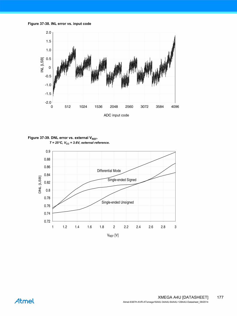
Figure 37-38. INL error vs. input code
Figure 37-39. DNL error vs. external VREF.T = 25°C, VCC = 3.6V, external reference.
-2.0
-1.5
-1.0
-0.5
0
0.5
1.0
1.5
2.0
0 512 1024 1536 2048 2560 3072 3584 4096
ADC input code
INL
[LS
B]
Single-ended Unsigned
Single-ended Signed
Differential Mode
0.72
0.74
0.76
0.78
0.8
0.82
0.84
0.86
0.88
0.9
1 1.2 1.4 1.6 1.8 2 2.2 2.4 2.6 2.8 3
DN
L [
LS
B]
V [V]REF
177XMEGA A4U [DATASHEET]Atmel-8387H-AVR-ATxmega16A4U-34A4U-64A4U-128A4U-Datasheet_09/2014

Figure 37-40. DNL error vs. sample rate.T = 25°C, VCC = 3.6V, VREF = 3.0V external.
Figure 37-41. DNL error vs. input code.
Single-ended Unsigned
Single-ended Signed
Differential Signed
0.79
0.8
0.81
0.82
0.83
0.84
0.85
0.86
0.87
0.88
0.89
0.9
500 650 800 950 1100 1250 1400 1550 1700 1850 2000
ADC Sample Rate [kSPS]
DN
L [LS
B]
-0.6
-0.4
-0.2
0
0.2
0.4
0.6
0.8
0 512 1024 1536 2048 2560 3072 3584 4096
ADC Input Code
DN
L [L
SB
]
178XMEGA A4U [DATASHEET]Atmel-8387H-AVR-ATxmega16A4U-34A4U-64A4U-128A4U-Datasheet_09/2014

Figure 37-42. Gain error vs. VREF.T = 25°C, VCC = 3.6V, ADC sampling speed = 500ksps.
Figure 37-43. Gain error vs. VCC.T = 25°C, VREF = external 1.0V, ADC sampling speed = 500ksps.
Single-ended Unsigned
Single-ended Signed
Differential Mode
-4
-3
-2
-1
0
1
2
3
1 1.2 1.4 1.6 1.8 2 2.2 2.4 2.6 2.8 3
V
Gain
Err
or
[mV
]
REF [V]
Single-ended Unsigned
Single-ended Signed
Differential Mode
-0.5
-0.2
0.1
0.4
0.7
1
1.3
1.6
1.9
2.2
1.6 1.8 2 2.2 2.4 2.6 2.8 3 3.2 3.4 3.6
VCC [V]
Gain
Err
or
[mV
]
179XMEGA A4U [DATASHEET]Atmel-8387H-AVR-ATxmega16A4U-34A4U-64A4U-128A4U-Datasheet_09/2014

Figure 37-44. Offset error vs. VREF.T = 25°C, VCC = 3.6V, ADC sampling speed = 500ksps.
Figure 37-45. Gain error vs. temperature.VCC = 3.0V, VREF = external 2.0V.
Differential Mode
-2
-1.9
-1.8
-1.7
-1.6
-1.5
-1.4
-1.3
-1.2
-1.1
-1
1 1.2 1.4 1.6 1.8 2 2.2 2.4 2.6 2.8 3
Off
set
Err
or
[mV
]
VREF [V]
Single-ended unsigned mode
Single-ended signed mode
Dif ferential mode
-4
-3
-2
-1
0
1
2
3
4
-45 -35 -25 -15 -5 5 15 25 35 45 55 65 75 85 95 105
Gai
n Er
ror [
mV]
Temperature [ºC]
180XMEGA A4U [DATASHEET]Atmel-8387H-AVR-ATxmega16A4U-34A4U-64A4U-128A4U-Datasheet_09/2014

Figure 37-46. Offset error vs. VCC.T = 25°C, VREF = external 1.0V, ADC sampling speed = 500ksps.
Figure 37-47. Noise vs. VREF.T = 25°C, VCC = 3.6V, ADC sampling speed = 500ksps.
Differential Signed
-1.2
-1.1
-1
-0.9
-0.8
-0.7
-0.6
-0.5
-0.4
-0.3
1.6 1.8 2 2.2 2.4 2.6 2.8 3 3.2 3.4 3.6
VCC [V]
Offset E
rror
[mV
]
Single-ended Unsigned
Single-ended Signed
Differential Signed
0.4
0.55
0.7
0.85
1
1.15
1.3
1 1.2 1.4 1.6 1.8 2 2.2 2.4 2.6 2.8 3
VREF [V]
Nois
e [m
V R
MS
]
181XMEGA A4U [DATASHEET]Atmel-8387H-AVR-ATxmega16A4U-34A4U-64A4U-128A4U-Datasheet_09/2014

Figure 37-48. Noise vs. VCC.T = 25°C, VREF = external 1.0V, ADC sampling speed = 500ksps.
37.1.4 DAC Characteristics
Figure 37-49. DAC INL error vs. VREF.VCC = 3.6V.
Single-ended Unsigned
Single-ended Signed
Differential Signed
0.3
0.4
0.5
0.6
0.7
0.8
0.9
1
1.1
1.2
1.3
1.6 1.8 2 2.2 2.4 2.6 2.8 3 3.2 3.4 3.6
VCC [V]
Nois
e [m
V R
MS
]
25°C
105°C85°C
-40°C
0.0
0.5
1.0
1.5
2.0
2.5
3.0
1.0 1.2 1.4 1.6 1.8 2.0 2.2 2.4 2.6 2.8 3.0
INL
[LSB
]
Vref [V]
182XMEGA A4U [DATASHEET]Atmel-8387H-AVR-ATxmega16A4U-34A4U-64A4U-128A4U-Datasheet_09/2014

Figure 37-50. DNL error vs. VREF.VCC = 3.6V.
Figure 37-51. DAC noise vs. temperature.VCC = 3.0V, VREF = 2.4V .
25ºC
105°C85°C
- 40°C
0.0
0.2
0.4
0.6
0.8
1.0
1.2
1.4
1.6
1.6 1.8 2.0 2.2 2.4 2.6 2.8 3.0
DN
L[LS
B]
Vref [V]
0.150
0.155
0.160
0.165
0.170
0.175
0.180
0.185
-45 -35 -25 -15 -5 5 15 25 35 45 55 65 75 85 95 105
Noi
se [m
V R
MS]
Temperature [ºC]
183XMEGA A4U [DATASHEET]Atmel-8387H-AVR-ATxmega16A4U-34A4U-64A4U-128A4U-Datasheet_09/2014

37.1.5 Analog Comparator Characteristics
Figure 37-52. Analog comparator hysteresis vs. VCC.High-speed, small hysteresis.
Figure 37-53. Analog comparator hysteresis vs. VCC.Low power, small hysteresis.
105 °C85 °C
25 °
C-40
°C
7
8
9
10
11
12
13
14
15
16
17
18
1.6 1.8 2 2.2 2.4 2.6 2.8 3 3.2 3.4 3.6
VH
YS
T[m
V]
VCC [V]
105 °C85 °C
25 °C
-40 °C
25
26
27
28
29
30
31
32
33
34
35
1.6 1.8 2 2.2 2.4 2.6 2.8 3 3.2 3.4 3.6
VH
YS
T[m
V]
VCC [V]
184XMEGA A4U [DATASHEET]Atmel-8387H-AVR-ATxmega16A4U-34A4U-64A4U-128A4U-Datasheet_09/2014

Figure 37-54. Analog comparator hysteresis vs. VCC.High-speed mode, large hysteresis.
Figure 37-55. Analog comparator hysteresis vs. VCC.Low power, large hysteresis.
105 °C85 °C
25 °C-40 °C
202224262830323436384042
1.6 1.8 2 2.2 2.4 2.6 2.8 3 3.2 3.4 3.6
VH
YS
T[m
V]
VCC [V]
105 °C
85 °C
25 °C
-40 °C
50
53
56
59
62
65
68
71
74
77
1.6 1.8 2 2.2 2.4 2.6 2.8 3 3.2 3.4 3.6
VH
YS
T[m
V]
VCC [V]
185XMEGA A4U [DATASHEET]Atmel-8387H-AVR-ATxmega16A4U-34A4U-64A4U-128A4U-Datasheet_09/2014

Figure 37-56. Analog comparator current source vs. calibration value.Temperature = 25°C.
Figure 37-57. Analog comparator current source vs. calibration value.VCC = 3.0V.
3.3 V3.0 V2.7 V
2.2 V1.8 V1.6 V2.0
2.6
3.2
3.8
4.4
5.0
5.6
6.2
6.8
7.4
0 1 2 3 4 5 6 7 8 9 10 11 12 13 14 15
I CU
RR
EN
TSO
UR
CE
[µA
]
CURRCALIBA[3..0]
105 °C85 °C25 °C
-40 °C
3
3.5
4
4.5
5
5.5
6
6.5
7
0 1 2 3 4 5 6 7 8 9 10 11 12 13 14 15
I CU
RR
EN
TSO
UR
CE
[uA
]
CURRCALIBA[3..0]
VCC 3.0V
186XMEGA A4U [DATASHEET]Atmel-8387H-AVR-ATxmega16A4U-34A4U-64A4U-128A4U-Datasheet_09/2014

Figure 37-58. Voltage scaler INL vs. SCALEFAC.T = 25°C, VCC = 3.0V.
37.1.6 Internal 1.0V reference Characteristics
Figure 37-59. ADC/DAC Internal 1.0V reference vs. temperature.
25°C
-0.150
-0.125
-0.100
-0.075
-0.050
-0.025
0
0.025
0.050
0 10 20 30 40 50 60 70
SCALEFAC
INL
[LS
B]
3.6 V3.0 V2.7 V2.2 V1.8 V1.6 V
0.986
0.988
0.990
0.992
0.994
0.996
0.998
1.000
1.002
1.004
-40 -25 -10 5 20 35 50 65 80 95 110
Ban
dgap
Vol
tage
[V]
Temperature [°C]
Calibrated at T 85 C
187XMEGA A4U [DATASHEET]Atmel-8387H-AVR-ATxmega16A4U-34A4U-64A4U-128A4U-Datasheet_09/2014

37.1.7 BOD Characteristics
Figure 37-60. BOD thresholds vs. temperature.BOD level = 1.6V.
Figure 37-61. BOD thresholds vs. temperature.BOD level = 3.0V.
Rising Vcc
Falling Vcc
1.600
1.605
1.610
1.615
1.620
1.625
1.630
1.635
-40 -25 -10 5 20 35 50 65 80 95 110
VB
OT
[V]
Temperature [°C]
Rising Vcc
Falling Vcc
2.97
2.98
2.99
3.00
3.01
3.02
3.03
3.04
3.05
3.06
-40 -25 -10 5 20 35 50 65 80 95 110
VB
OT
[V]
Temperature [°C]
188XMEGA A4U [DATASHEET]Atmel-8387H-AVR-ATxmega16A4U-34A4U-64A4U-128A4U-Datasheet_09/2014

37.1.8 External Reset Characteristics
Figure 37-62. Minimum Reset pin pulse width vs. VCC.
Figure 37-63. Reset pin pull-up resistor current vs. reset pin voltage.VCC = 1.8V.
105 °C85 °C
25 °C-40 °C
80
85
90
95
100
105
110
115
120
125
130
1.6 1.8 2.0 2.2 2.4 2.6 2.8 3.0 3.2 3.4 3.6
t RS
T[n
s]
VCC [V]
105 °C85 °C25 °C
-40 °C
0
8
16
24
32
40
48
56
64
72
0.0 0.2 0.4 0.6 0.8 1.0 1.2 1.4 1.6 1.8
I RE
SE
T[u
A]
VRESET [V]
189XMEGA A4U [DATASHEET]Atmel-8387H-AVR-ATxmega16A4U-34A4U-64A4U-128A4U-Datasheet_09/2014

Figure 37-64. Reset pin pull-up resistor current vs. reset pin voltage.VCC = 3.0V.
Figure 37-65. Reset pin pull-up resistor current vs. reset pin voltage.VCC = 3.3V.
105 °C85 °C25 °C
-40 °C
0
15
30
45
60
75
90
105
120
0.0 0.3 0.6 0.9 1.2 1.5 1.8 2.1 2.4 2.7 3.0
I RE
SE
T[µ
A]
VRESET [V]
105 °C85 °C25 °C-40 °C
0
20
40
60
80
100
120
140
0.0 0.3 0.6 0.9 1.2 1.5 1.8 2.1 2.4 2.7 3.0 3.3
I RE
SE
T[u
A]
VRESET [V]
190XMEGA A4U [DATASHEET]Atmel-8387H-AVR-ATxmega16A4U-34A4U-64A4U-128A4U-Datasheet_09/2014

Figure 37-66. Reset pin input threshold voltage vs. VCC.VIH - Reset pin read as “1”.
Figure 37-67. Reset pin input threshold voltage vs. VCC.VIL - Reset pin read as “0”.
105 °C85 °C25 °C-40 °C
1.00
1.15
1.30
1.45
1.60
1.75
1.90
2.05
2.20
1.6 1.8 2.0 2.2 2.4 2.6 2.8 3.0 3.2 3.4 3.6
Vth
resh
old
[V]
VCC [V]
105 °C85 °C25 °C
-40 °C
0.40
0.55
0.70
0.85
1.00
1.15
1.30
1.45
1.60
1.75
1.6 1.8 2.0 2.2 2.4 2.6 2.8 3.0 3.2 3.4 3.6
Vth
resh
old
[V]
VCC [V]
191XMEGA A4U [DATASHEET]Atmel-8387H-AVR-ATxmega16A4U-34A4U-64A4U-128A4U-Datasheet_09/2014
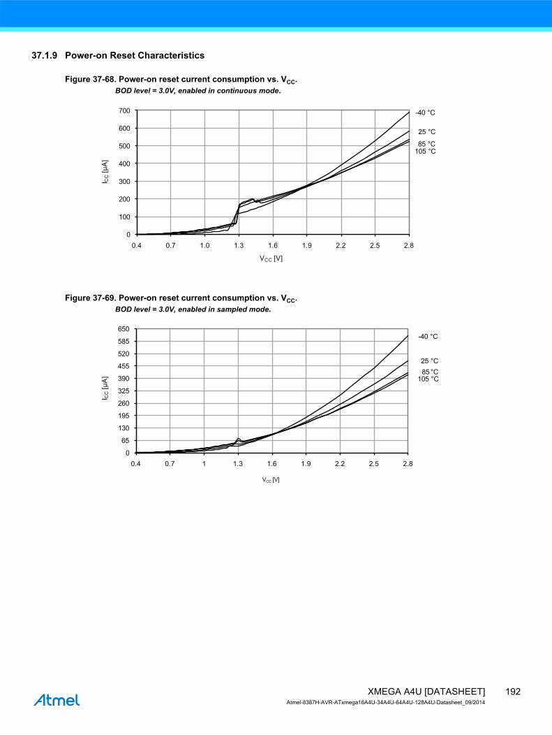
37.1.9 Power-on Reset Characteristics
Figure 37-68. Power-on reset current consumption vs. VCC.BOD level = 3.0V, enabled in continuous mode.
Figure 37-69. Power-on reset current consumption vs. VCC.BOD level = 3.0V, enabled in sampled mode.
105 °C85 °C
25 °C
-40 °C
0
100
200
300
400
500
600
700
0.4 0.7 1.0 1.3 1.6 1.9 2.2 2.5 2.8
I CC
[µA
]
VCC [V]
105 °°C85 ° °C25 °C
-40 °C
0
65
130
195
260
325
390
455
520
585
650
0.4 0.7 1 1.3 1.6 1.9 2.2 2.5 2.8
I CC
[µA
]
VCC [V]
192XMEGA A4U [DATASHEET]Atmel-8387H-AVR-ATxmega16A4U-34A4U-64A4U-128A4U-Datasheet_09/2014

37.1.10 Oscillator Characteristics
37.1.10.1 Ultra Low-Power internal oscillator
Figure 37-70. Ultra Low-Power internal oscillator frequency vs. temperature.
37.1.10.2 32.768kHz Internal Oscillator
Figure 37-71. 32.768kHz internal oscillator frequency vs. temperature.
3.6 V3.0 V2.7 V2.2 V1.8 V1.6 V
29.6
30.0
30.4
30.8
31.2
31.6
32.0
32.4
32.8
-40 -25 -10 5 20 35 50 65 80 95 110
Freq
uenc
y [k
Hz]
Temperature [°C]
3.6 V3.0 V
2.7 V2.2 V
1.8 V1.6 V
32.650
32.675
32.700
32.725
32.750
32.775
32.800
32.825
32.850
32.875
-40 -25 -10 5 20 35 50 65 80 95 110
Freq
uenc
y [k
Hz]
Temperature [°C]
193XMEGA A4U [DATASHEET]Atmel-8387H-AVR-ATxmega16A4U-34A4U-64A4U-128A4U-Datasheet_09/2014

Figure 37-72. 32.768kHz internal oscillator frequency vs. calibration value.VCC = 3.0V, T = 25°C.
37.1.10.3 2MHz Internal Oscillator
Figure 37-73. 2MHz internal oscillator frequency vs. temperature.DFLL disabled.
20
25
30
35
40
45
50
55
0 26 52 78 104 130 156 182 208 234 260
Freq
uenc
y [k
Hz]
RC32KCAL[7..0]
3.6 V3.0 V2.7 V2.2 V1.8 V1.6 V1.96
1.98
2.00
2.02
2.04
2.06
2.08
2.10
2.12
2.14
2.16
-40 -25 -10 5 20 35 50 65 80 95 110
Freq
uenc
y [M
Hz]
Temperature [°C]
194XMEGA A4U [DATASHEET]Atmel-8387H-AVR-ATxmega16A4U-34A4U-64A4U-128A4U-Datasheet_09/2014

Figure 37-74. 2MHz internal oscillator frequency vs. temperature.DFLL enabled, from the 32.768kHz internal oscillator .
Figure 37-75. 2MHz internal oscillator CALA calibration step size.VCC = 3V.
3.6 V
3.0 V2.7 V
2.2 V1.8 V
1.6 V
1.9950
1.9965
1.9980
1.9995
2.0010
2.0025
2.0040
2.0055
2.0070
2.0085
-40 -25 -10 5 20 35 50 65 80 95 110
Freq
uenc
y [M
Hz]
Temperature [°C]
105 °C85 °C25 °C
-40 °C
0.15 %
0.17 %
0.19 %
0.21 %
0.23 %
0.25 %
0.27 %
0.29 %
0.31 %
0 16 32 48 64 80 96 112 128
Freq
uenc
y S
tep
size
[%]
CALA
195XMEGA A4U [DATASHEET]Atmel-8387H-AVR-ATxmega16A4U-34A4U-64A4U-128A4U-Datasheet_09/2014

37.1.10.4 32MHz Internal Oscillator
Figure 37-76. 32MHz internal oscillator frequency vs. temperature.DFLL disabled.
Figure 37-77. 32MHz internal oscillator frequency vs. temperature.DFLL enabled, from the 32.768kHz internal oscillator.
3.6 V3.0 V2.7 V2.2 V1.8 V1.6 V
31.0
31.5
32.0
32.5
33.0
33.5
34.0
34.5
35.0
35.5
36.0
-40 -25 -10 5 20 35 50 65 80 95 110
Freq
uenc
y [M
Hz]
Temperature [°C]
3.6 V
3.0 V2.7 V2.2 V1.8 V1.6 V
31.920
31.945
31.970
31.995
32.020
32.045
32.070
32.095
32.120
32.145
-40 -25 -10 5 20 35 50 65 80 95 110
Freq
uenc
y [M
Hz]
Temperature [°C]
1.6 V
196XMEGA A4U [DATASHEET]Atmel-8387H-AVR-ATxmega16A4U-34A4U-64A4U-128A4U-Datasheet_09/2014

Figure 37-78. 32MHz internal oscillator CALA calibration step size.VCC = 3.0V.
Figure 37-79. 32MHz internal oscillator frequency vs. CALB calibration value.VCC = 3.0V.
105 °C85 °C
25 °C-40 °C
0.10 %
0.14 %
0.18 %
0.22 %
0.26 %
0.30 %
0.34 %
0.38 %
0 16 32 48 64 80 96 112 128
Freq
uenc
y S
tep
size
[%]
CALA
105°C85°C25°C
- 40°C
25
30
35
40
45
50
55
60
65
70
75
0 8 16 24 32 40 48 56 64
Freq
uenc
y [M
Hz]
CALB
197XMEGA A4U [DATASHEET]Atmel-8387H-AVR-ATxmega16A4U-34A4U-64A4U-128A4U-Datasheet_09/2014

37.1.10.5 32MHz internal oscillator calibrated to 48MHz
Figure 37-80. 48MHz internal oscillator frequency vs. temperature.DFLL disabled.
Figure 37-81. 48MHz internal oscillator frequency vs. temperature.DFLL enabled, from the 32.768kHz internal oscillator.
3.6 V3.0 V2.7 V2.2 V1.8 V1.6 V
46
47
48
49
50
51
52
53
54
-40 -25 -10 5 20 35 50 65 80 95 110
Freq
uenc
y [M
Hz]
Temperature [°C]
3.6 V
3.0 V
2.7 V2.2 V
1.8 V1.6 V
47.80
47.85
47.90
47.95
48.00
48.05
48.10
48.15
48.20
48.25
-40 -25 -10 5 20 35 50 65 80 95 110
Freq
uenc
y [M
Hz]
Temperature [°C]
198XMEGA A4U [DATASHEET]Atmel-8387H-AVR-ATxmega16A4U-34A4U-64A4U-128A4U-Datasheet_09/2014

Figure 37-82. 48MHz internal oscillator CALA calibration step size.VCC = 3.0V.
37.1.11 Two-Wire Interface characteristics
Figure 37-83. SDA hold time vs. supply voltage.
105 °C85 °C25 °C-40 °C
0.10 %
0.13 %
0.16 %
0.19 %
0.22 %
0.25 %
0.28 %
0.31 %
0.34 %
0 16 32 48 64 80 96 112 128
Freq
uenc
y S
tep
size
[%]
CALA
VCC 3.0 V
105°C
85°C
25°C
- 40°C260
265
270
275
280
285
290
295
300
2.6 2.7 2.8 2.9 3.0 3.1 3.2 3.3 3.4 3.5 3.6
Hol
dtim
e [n
s]
Vcc [V]
199XMEGA A4U [DATASHEET]Atmel-8387H-AVR-ATxmega16A4U-34A4U-64A4U-128A4U-Datasheet_09/2014

37.1.12 PDI characteristics
Figure 37-84. Maximum PDI frequency vs. VCC.
105 °C
85 °C
25 °C
-40 °C
10
13
16
19
22
25
28
31
34
1.6 1.8 2 2.2 2.4 2.6 2.8 3 3.2 3.4 3.6
f MA
X[M
Hz]
VCC [V]
200XMEGA A4U [DATASHEET]Atmel-8387H-AVR-ATxmega16A4U-34A4U-64A4U-128A4U-Datasheet_09/2014

37.2 ATxmega32A4U
37.2.1 Current consumption
37.2.1.1 Active mode supply current
Figure 37-85.Active supply current vs. frequency.fSYS = 0 - 1MHz external clock, T = 25°C.
Figure 37-86.Active supply current vs. frequency.fSYS = 1 - 32MHz external clock, T = 25°C.
3.3V
3.0V
2.7V
2.2V
1.8V
0
60
120
180
240
300
360
420
480
540
600
0 0.1 0.2 0.3 0.4 0.5 0.6 0.7 0.8 0.9 1
Frequency [MHz]
ICC [µ
A]
3.3V
3.0V
2.7V
0
2
4
6
8
10
12
0 4 8 12 16 20 24 28 32
Frequency [MHz]
I CC [m
A]
2.2V
1.8V
201XMEGA A4U [DATASHEET]Atmel-8387H-AVR-ATxmega16A4U-34A4U-64A4U-128A4U-Datasheet_09/2014

Figure 37-87.Active mode supply current vs. VCC.fSYS = 32.768kHz internal oscillator.
Figure 37-88.Active mode supply current vs. VCC.fSYS = 1MHz external clock.
105 °C85 °C
25 °C
-40 °C
70
90
110
130
150
170
190
210
230
250
270
1.6 1.8 2 2.2 2.4 2.6 2.8 3 3.2 3.4 3.6
I CC
[uA
]
VCC [V]
105 °C85 °C25 °C-40 °C
200
300
400
500
600
700
800
1.6 1.8 2 2.2 2.4 2.6 2.8 3 3.2 3.4 3.6
I CC
[uA
]
VCC [V]
202XMEGA A4U [DATASHEET]Atmel-8387H-AVR-ATxmega16A4U-34A4U-64A4U-128A4U-Datasheet_09/2014

Figure 37-89.Active mode supply current vs. VCC.fSYS = 2MHz internal oscillator.
Figure 37-90.Active mode supply current vs. VCC.fSYS = 32MHz internal oscillator prescaled to 8MHz.
105 °C85 °C25 °C-40 °C
400
600
800
1000
1200
1400
1600
1.6 1.8 2 2.2 2.4 2.6 2.8 3 3.2 3.4 3.6
I CC
[uA
]
VCC [V]
105 °C85 °C25 °C-40 °C
1400
1900
2400
2900
3400
3900
4400
4900
5400
5900
1.6 1.8 2 2.2 2.4 2.6 2.8 3 3.2 3.4 3.6
I CC
[uA
]
VCC [V]
203XMEGA A4U [DATASHEET]Atmel-8387H-AVR-ATxmega16A4U-34A4U-64A4U-128A4U-Datasheet_09/2014

Figure 37-91.Active mode supply current vs. VCC.fSYS = 32MHz internal oscillator.
37.2.1.2 Idle mode supply current
Figure 37-92.Idle mode supply current vs. frequency.fSYS = 0 - 1MHz external clock, T = 25°C.
105 °C85 °C
25 °C
-40 °C
3400
3625
3850
4075
4300
4525
4750
4975
5200
5425
5650
2.7 2.8 2.9 3 3.1 3.2 3.3 3.4 3.5 3.6
I CC
[uA
]
VCC [V]
3.3V
3.0V
2.7V
2.2V
1.8V
0
20
40
60
80
100
120
140
0 0.1 0.2 0.3 0.4 0.5 0.6 0.7 0.8 0.9 1.0
Frequency [MHz]
I CC [µ
A]
204XMEGA A4U [DATASHEET]Atmel-8387H-AVR-ATxmega16A4U-34A4U-64A4U-128A4U-Datasheet_09/2014

Figure 37-93.Idle mode supply current vs. frequency.fSYS = 1 - 32MHz external clock, T = 25°C.
Figure 37-94. Idle mode supply current vs. VCC.fSYS = 32.768kHz internal oscillator.
3.3V
3.0V
2.7V
0
0.5
1.0
1.5
2.0
2.5
3.0
3.5
4.0
4.5
0 4 8 12 16 20 24 28 32
Frequency [MHz]
I CC [m
A]
2.2V
1.8V
105 °C
85 °C25 °C
-40 °C
27
28
29
30
31
32
33
34
35
1.6 1.8 2 2.2 2.4 2.6 2.8 3 3.2 3.4 3.6
I CC
[uA
]
VCC [V]
205XMEGA A4U [DATASHEET]Atmel-8387H-AVR-ATxmega16A4U-34A4U-64A4U-128A4U-Datasheet_09/2014

Figure 37-95. Idle mode supply current vs. VCC.fSYS = 1MHz external clock.
Figure 37-96. Idle mode supply current vs. VCC.fSYS = 2MHz internal oscillator.
105 °C85 °C25 °C-40 °C
50
62
74
86
98
110
122
134
146
158
1.6 1.8 2 2.2 2.4 2.6 2.8 3 3.2 3.4 3.6
I CC
[uA
]
VCC [V]
105 °C85 °C25 °C-40 °C
160
185
210
235
260
285
310
335
360
385
410
1.6 1.8 2 2.2 2.4 2.6 2.8 3 3.2 3.4 3.6
I CC
[uA
]
VCC [V]
206XMEGA A4U [DATASHEET]Atmel-8387H-AVR-ATxmega16A4U-34A4U-64A4U-128A4U-Datasheet_09/2014

Figure 37-97. Idle mode supply current vs. VCC.fSYS = 32MHz internal oscillator prescaled to 8MHz.
Figure 37-98. Idle mode current vs. VCC.fSYS = 32MHz internal oscillator.
105 °C85 °C25 °C-40 °C
600
800
1000
1200
1400
1600
1800
2000
1.6 1.8 2 2.2 2.4 2.6 2.8 3 3.2 3.4 3.6
I CC
[uA
]
VCC [V]
105 °C85 °C
25 °C
-40 °C
3400
3625
3850
4075
4300
4525
4750
4975
5200
5425
5650
2.7 2.8 2.9 3 3.1 3.2 3.3 3.4 3.5 3.6
I CC
[uA
]
VCC [V]
207XMEGA A4U [DATASHEET]Atmel-8387H-AVR-ATxmega16A4U-34A4U-64A4U-128A4U-Datasheet_09/2014

37.2.1.3 Power-down mode supply current
Figure 37-99. Power-down mode supply current vs. temperature.All functions disabled.
Figure 37-100. Power-down mode supply current vs. VCC.All functions disabled.
3.6 V
3.0 V2.7 V2.2 V1.8 V1.6 V
0.00
0.50
1.00
1.50
2.00
2.50
3.00
3.50
-40 -25 -10 5 20 35 50 65 80 95 110
I CC
[uA
]
Temperature [°C]
105 °C
85 °C
25 °C-40 °C0.0
0.4
0.8
1.2
1.6
2.0
2.4
2.8
3.2
3.6
1.6 1.8 2 2.2 2.4 2.6 2.8 3 3.2 3.4 3.6
ICC
[uA
]
VCC [V]
208XMEGA A4U [DATASHEET]Atmel-8387H-AVR-ATxmega16A4U-34A4U-64A4U-128A4U-Datasheet_09/2014

Figure 37-101. Power-down mode supply current vs. VCC.Watchdog and sampled BOD enabled.
37.2.1.4 Power-save mode supply current
Figure 37-102. Power-save mode supply current vs.VCC.Real Time Counter enabled and running from 1.024kHz output of 32.768kHz TOSC.
105 °C
85 °C
25 °C-40 °C
1.1
1.6
2.1
2.6
3.1
3.6
4.1
4.6
5.1
1.6 1.8 2.0 2.2 2.4 2.6 2.8 3.0 3.2 3.4 3.6
I CC
[µA
]
VCC [V]
Normal mode
Low-power mode
0
0.1
0.2
0.3
0.4
0.5
0.6
0.7
0.8
0.9
VCC [V]
I CC
[µA
]
1.6 1.8 2.0 2.2 2.4 2.6 2.8 3.0 3.2 3.4 3.6
209XMEGA A4U [DATASHEET]Atmel-8387H-AVR-ATxmega16A4U-34A4U-64A4U-128A4U-Datasheet_09/2014

37.2.1.5 Standby mode supply current
Figure 37-103. Standby supply current vs. VCC.Standby, fSYS = 1MHz.
Figure 37-104. Standby supply current vs. VCC.25°C, running from different crystal oscillators.
105 °C
85 °C
25 °C-40 °C
2.5
3.5
4.5
5.5
6.5
7.5
8.5
9.5
10.5
11.5
12.5
1.6 1.8 2 2.2 2.4 2.6 2.8 3 3.2 3.4 3.6
I CC
[uA
]
VCC [V]
16MHz12MHz
8MHz
2MHz
0.454MHz
160
200
240
280
320
360
400
440
480
1.6 1.8 2 2.2 2.4 2.6 2.8 3 3.2 3.4 3.6
VCC [V]
ICC
[µA
]
210XMEGA A4U [DATASHEET]Atmel-8387H-AVR-ATxmega16A4U-34A4U-64A4U-128A4U-Datasheet_09/2014

37.2.2 I/O Pin Characteristics
37.2.2.1 Pull-up
Figure 37-105. I/O pin pull-up resistor current vs. input voltage.VCC = 1.8V.
Figure 37-106. I/O pin pull-up resistor current vs. input voltage.VCC = 3.0V.
105 °C85 °C25 °C
-40 °C
0
8
16
24
32
40
48
56
64
72
0.0 0.2 0.4 0.6 0.8 1.0 1.2 1.4 1.6 1.8
I [µA
]
VPIN [V]
105 °C85 °C25 °C
-40 °C
0
15
30
45
60
75
90
105
120
0.0 0.3 0.6 0.9 1.2 1.5 1.8 2.1 2.4 2.7 3.0
I [µA
]
VPIN [V]
211XMEGA A4U [DATASHEET]Atmel-8387H-AVR-ATxmega16A4U-34A4U-64A4U-128A4U-Datasheet_09/2014

Figure 37-107. I/O pin pull-up resistor current vs. input voltage.VCC = 3.3V.
37.2.2.2 Output Voltage vs. Sink/Source Current
Figure 37-108. I/O pin output voltage vs. source current.VCC = 1.8V.
105 °C85 °C25 °C
-40 °C
0
15
30
45
60
75
90
105
120
135
0.0 0.3 0.6 0.9 1.2 1.5 1.8 2.1 2.4 2.7 3.0 3.3
I [µA
]
VPIN [V]
105 °C85 °C
25 °C-40 °C
0.0
0.2
0.4
0.6
0.8
1.0
1.2
1.4
1.6
1.8
-10 -9 -8 -7 -6 -5 -4 -3 -2 -1 0
VP
IN[V
]
IPIN [mA]
212XMEGA A4U [DATASHEET]Atmel-8387H-AVR-ATxmega16A4U-34A4U-64A4U-128A4U-Datasheet_09/2014

Figure 37-109. I/O pin output voltage vs. source current.VCC = 3.0V.
Figure 37-110. I/O pin output voltage vs. source current.VCC = 3.3V.
105 °C85 °C25 °C
-40 °C
0.0
0.3
0.6
0.9
1.2
1.5
1.8
2.1
2.4
2.7
3.0
-32 -28 -24 -20 -16 -12 -8 -4 0
VP
IN[V
]
IPIN [mA]
105 °C85 °C
25 °C
-40 °C
0.00.30.60.91.21.51.82.12.42.73.03.3
-32 -28 -24 -20 -16 -12 -8 -4 0
VP
IN[V
]
IPIN [mA]
213XMEGA A4U [DATASHEET]Atmel-8387H-AVR-ATxmega16A4U-34A4U-64A4U-128A4U-Datasheet_09/2014

Figure 37-111. I/O pin output voltage vs. source current.
Figure 37-112. I/O pin output voltage vs. sink current.VCC = 1.8V.
3.6V
3.3V
3.0V
2.7V
2.3V
1.8V
0.5
1.0
1.5
2.0
2.5
3.0
3.5
4.0
-24 -21 -18 -15 -12 -9 -6 -3 0
IPIN [mA]
VP
IN [V
]
105 °C85 °C
25 °C
-40 °C
0.0
0.1
0.2
0.3
0.4
0.5
0.6
0.7
0.8
0.9
1.0
0 2 4 6 8 10 12 14 16
VP
IN[V
]
IPIN [mA]
214XMEGA A4U [DATASHEET]Atmel-8387H-AVR-ATxmega16A4U-34A4U-64A4U-128A4U-Datasheet_09/2014

Figure 37-113. I/O pin output voltage vs. sink current.VCC = 3.0V.
Figure 37-114. I/O pin output voltage vs. sink current.VCC = 3.3V.
Figure 37-115. I/O pin output voltage vs. sink current.
105 °C85 °C25 °C-40 °C
0.0
0.1
0.2
0.3
0.4
0.5
0.6
0.7
0 2 4 6 8 10 12 14 16 18 20
VP
IN[V
]
IPIN [mA]
105 °C85 °C
25 °C-40 °C
0.0
0.1
0.2
0.3
0.4
0.5
0.6
0.7
0.8
0.9
1.0
0 4 8 12 16 20 24 28 32
VP
IN[V
]
IPIN [mA]
0
0.3
0.6
0.9
1.2
1.5
0 5 10 15 20 25 30
IPIN [mA]
VP
IN [
V]
1.8V
3.6V3.3V3.0V2.7V
2.3V
215XMEGA A4U [DATASHEET]Atmel-8387H-AVR-ATxmega16A4U-34A4U-64A4U-128A4U-Datasheet_09/2014

37.2.2.3 Thresholds and Hysteresis
Figure 37-116. I/O pin input threshold voltage vs. VCC.T = 25°C.
Figure 37-117. I/O pin input threshold voltage vs. VCC.VIH I/O pin read as “1”.
VIL
VIH
0.0
0.2
0.4
0.6
0.8
1.0
1.2
1.4
1.6
1.8
1.6 1.8 2 2.2 2.4 2.6 2.8 3 3.2 3.4 3.6
Vcc [V]
Vth
reshold
[V
]
105 °C85 °C25 °C
-40 °C
0.8
0.9
1.0
1.1
1.2
1.3
1.4
1.5
1.6
1.7
1.8
1.6 1.8 2.0 2.2 2.4 2.6 2.8 3.0 3.2 3.4 3.6
Vth
resh
old
[V]
VCC [V]
216XMEGA A4U [DATASHEET]Atmel-8387H-AVR-ATxmega16A4U-34A4U-64A4U-128A4U-Datasheet_09/2014

Figure 37-118. I/O pin input threshold voltage vs. VCC.VIL I/O pin read as “0”.
Figure 37-119. I/O pin input hysteresis vs. VCC.
105 °C85 °C25 °C
-40 °C
0.55
0.70
0.85
1.00
1.15
1.30
1.45
1.60
1.75
1.6 1.8 2.0 2.2 2.4 2.6 2.8 3.0 3.2 3.4 3.6
Vth
resh
old
[V]
VCC [V]
105 °C
85 °C
25 °C -40 °C
0.08
0.11
0.14
0.17
0.20
0.23
0.26
0.29
0.32
1.6 1.8 2.0 2.2 2.4 2.6 2.8 3.0 3.2 3.4 3.6
Vth
resh
old
[V]
VCC [V]
217XMEGA A4U [DATASHEET]Atmel-8387H-AVR-ATxmega16A4U-34A4U-64A4U-128A4U-Datasheet_09/2014

37.2.3 ADC Characteristics
Figure 37-120. INL error vs. external VREF.T = 25°C, VCC = 3.6V, external reference.
Figure 37-121. INL error vs. sample rate.T = 25°C, VCC = 3.6V, VREF = 3.0V external.
Single-ended Unsigned
Single-ended Signed
Differential Signed
0.7
0.8
0.9
1
1.1
1.2
1.3
1.4
1.5
1.6
1.7
1.8
1 1.2 1.4 1.6 1.8 2 2.2 2.4 2.6 2.8 3
V [V]
INL [
LS
B]
REF
Single-ended Unsigned
Single-ended Signed
Differential Mode
0.9
0.95
1
1.05
1.1
1.15
1.2
1.25
1.3
1.35
1.4
500 650 800 950 1100 1250 1400 1550 1700 1850 2000
ADC Sample Rate [kSPS]
INL [
LS
B]
218XMEGA A4U [DATASHEET]Atmel-8387H-AVR-ATxmega16A4U-34A4U-64A4U-128A4U-Datasheet_09/2014

Figure 37-122. INL error vs. input code
Figure 37-123. DNL error vs. external VREF.T = 25°C, VCC = 3.6V, external reference.
-2.0
-1.5
-1.0
-0.5
0
0.5
1.0
1.5
2.0
0 512 1024 1536 2048 2560 3072 3584 4096
ADC input code
INL
[LS
B]
Single-ended Unsigned
Single-ended Signed
Differential Mode
0.72
0.74
0.76
0.78
0.8
0.82
0.84
0.86
0.88
0.9
1 1.2 1.4 1.6 1.8 2 2.2 2.4 2.6 2.8 3
DN
L [
LS
B]
V [V]REF
219XMEGA A4U [DATASHEET]Atmel-8387H-AVR-ATxmega16A4U-34A4U-64A4U-128A4U-Datasheet_09/2014

Figure 37-124. DNL error vs. sample rate.T = 25°C, VCC = 3.6V, VREF = 3.0V external.
Figure 37-125. DNL error vs. input code.
Single-ended Unsigned
Single-ended Signed
Differential Signed
0.79
0.8
0.81
0.82
0.83
0.84
0.85
0.86
0.87
0.88
0.89
0.9
500 650 800 950 1100 1250 1400 1550 1700 1850 2000
ADC Sample Rate [kSPS]
DN
L [LS
B]
-0.6
-0.4
-0.2
0
0.2
0.4
0.6
0.8
0 512 1024 1536 2048 2560 3072 3584 4096
ADC Input Code
DN
L [L
SB
]
220XMEGA A4U [DATASHEET]Atmel-8387H-AVR-ATxmega16A4U-34A4U-64A4U-128A4U-Datasheet_09/2014

Figure 37-126. Gain error vs. VREF.T = 25°C, VCC = 3.6V, ADC sampling speed = 500ksps.
Figure 37-127. Gain error vs. VCC.T = 25°C, VREF = external 1.0V, ADC sampling speed = 500ksps.
Single-ended Unsigned
Single-ended Signed
Differential Mode
-4
-3
-2
-1
0
1
2
3
1 1.2 1.4 1.6 1.8 2 2.2 2.4 2.6 2.8 3
V
Gain
Err
or
[mV
]
REF [V]
Single-ended Unsigned
Single-ended Signed
Differential Mode
-0.5
-0.2
0.1
0.4
0.7
1
1.3
1.6
1.9
2.2
1.6 1.8 2 2.2 2.4 2.6 2.8 3 3.2 3.4 3.6
VCC [V]
Gain
Err
or
[mV
]
221XMEGA A4U [DATASHEET]Atmel-8387H-AVR-ATxmega16A4U-34A4U-64A4U-128A4U-Datasheet_09/2014

Figure 37-128. Offset error vs. VREF.T = 25°C, VCC = 3.6V, ADC sampling speed = 500ksps.
Figure 37-129. Gain error vs. temperature.VCC = 3.0V, VREF = external 2.0V.
Differential Mode
-2
-1.9
-1.8
-1.7
-1.6
-1.5
-1.4
-1.3
-1.2
-1.1
-1
1 1.2 1.4 1.6 1.8 2 2.2 2.4 2.6 2.8 3
Off
set
Err
or
[mV
]
VREF [V]
Single-ended unsigned mode
Single-ended signed mode
Dif ferential mode
-4
-3
-2
-1
0
1
2
3
4
-45 -35 -25 -15 -5 5 15 25 35 45 55 65 75 85 95 105
Gai
n Er
ror [
mV]
Temperature [ºC]
222XMEGA A4U [DATASHEET]Atmel-8387H-AVR-ATxmega16A4U-34A4U-64A4U-128A4U-Datasheet_09/2014

Figure 37-130. Offset error vs. VCC.T = 25°C, VREF = external 1.0V, ADC sampling speed = 500ksps.
Figure 37-131. Noise vs. VREF.T = 25°C, VCC = 3.6V, ADC sampling speed = 500ksps.
Differential Signed
-1.2
-1.1
-1
-0.9
-0.8
-0.7
-0.6
-0.5
-0.4
-0.3
1.6 1.8 2 2.2 2.4 2.6 2.8 3 3.2 3.4 3.6
VCC [V]
Offset E
rror
[mV
]
Single-ended Unsigned
Single-ended Signed
Differential Signed
0.4
0.55
0.7
0.85
1
1.15
1.3
1 1.2 1.4 1.6 1.8 2 2.2 2.4 2.6 2.8 3
VREF [V]
Nois
e [m
V R
MS
]
223XMEGA A4U [DATASHEET]Atmel-8387H-AVR-ATxmega16A4U-34A4U-64A4U-128A4U-Datasheet_09/2014
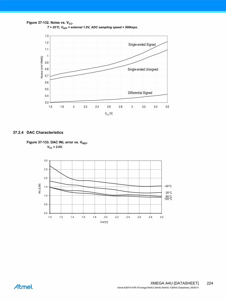
Figure 37-132. Noise vs. VCC.T = 25°C, VREF = external 1.0V, ADC sampling speed = 500ksps.
37.2.4 DAC Characteristics
Figure 37-133. DAC INL error vs. VREF.VCC = 3.6V.
Single-ended Unsigned
Single-ended Signed
Differential Signed
0.3
0.4
0.5
0.6
0.7
0.8
0.9
1
1.1
1.2
1.3
1.6 1.8 2 2.2 2.4 2.6 2.8 3 3.2 3.4 3.6
VCC [V]
Nois
e [m
V R
MS
]
25°C
105°C85°C
-40°C
0.0
0.5
1.0
1.5
2.0
2.5
3.0
1.0 1.2 1.4 1.6 1.8 2.0 2.2 2.4 2.6 2.8 3.0
INL
[LSB
]
Vref [V]
224XMEGA A4U [DATASHEET]Atmel-8387H-AVR-ATxmega16A4U-34A4U-64A4U-128A4U-Datasheet_09/2014
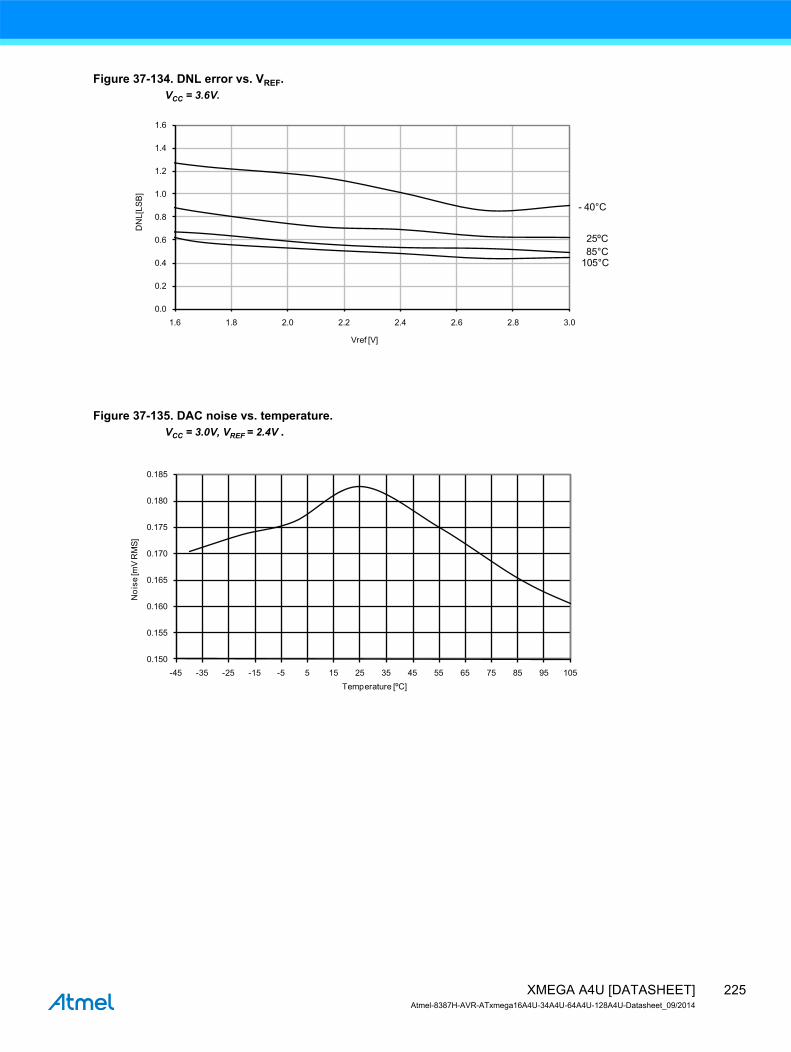
Figure 37-134. DNL error vs. VREF.VCC = 3.6V.
Figure 37-135. DAC noise vs. temperature.VCC = 3.0V, VREF = 2.4V .
25ºC
105°C85°C
- 40°C
0.0
0.2
0.4
0.6
0.8
1.0
1.2
1.4
1.6
1.6 1.8 2.0 2.2 2.4 2.6 2.8 3.0
DN
L[LS
B]
Vref [V]
0.150
0.155
0.160
0.165
0.170
0.175
0.180
0.185
-45 -35 -25 -15 -5 5 15 25 35 45 55 65 75 85 95 105
Noi
se [m
V R
MS]
Temperature [ºC]
225XMEGA A4U [DATASHEET]Atmel-8387H-AVR-ATxmega16A4U-34A4U-64A4U-128A4U-Datasheet_09/2014

37.2.5 Analog Comparator Characteristics
Figure 37-136. Analog comparator hysteresis vs. VCC.High-speed, small hysteresis.
Figure 37-137. Analog comparator hysteresis vs. VCC.Low power, small hysteresis.
105 °C85 °C
25 °
C-40
°C
7
8
9
10
11
12
13
14
15
16
17
18
1.6 1.8 2 2.2 2.4 2.6 2.8 3 3.2 3.4 3.6
VH
YS
T[m
V]
VCC [V]
105 °C85 °C
25 °C
-40 °C
25
26
27
28
29
30
31
32
33
34
35
1.6 1.8 2 2.2 2.4 2.6 2.8 3 3.2 3.4 3.6
VH
YS
T[m
V]
VCC [V]
226XMEGA A4U [DATASHEET]Atmel-8387H-AVR-ATxmega16A4U-34A4U-64A4U-128A4U-Datasheet_09/2014

Figure 37-138. Analog comparator hysteresis vs. VCC.High-speed mode, large hysteresis.
Figure 37-139. Analog comparator hysteresis vs. VCC.Low power, large hysteresis.
105 °C85 °C
25 °C-40 °C
202224262830323436384042
1.6 1.8 2 2.2 2.4 2.6 2.8 3 3.2 3.4 3.6
VH
YS
T[m
V]
VCC [V]
105 °C
85 °C
25 °C
-40 °C
50
53
56
59
62
65
68
71
74
77
1.6 1.8 2 2.2 2.4 2.6 2.8 3 3.2 3.4 3.6
VH
YS
T[m
V]
VCC [V]
227XMEGA A4U [DATASHEET]Atmel-8387H-AVR-ATxmega16A4U-34A4U-64A4U-128A4U-Datasheet_09/2014

Figure 37-140. Analog comparator current source vs. calibration value.Temperature = 25°C.
Figure 37-141. Analog comparator current source vs. calibration value.VCC = 3.0V.
3.3 V3.0 V2.7 V
2.2 V1.8 V1.6 V2.0
2.6
3.2
3.8
4.4
5.0
5.6
6.2
6.8
7.4
0 1 2 3 4 5 6 7 8 9 10 11 12 13 14 15
I CU
RR
EN
TSO
UR
CE
[µA
]
CURRCALIBA[3..0]
105 °C85 °C25 °C
-40 °C
3
3.5
4
4.5
5
5.5
6
6.5
7
0 1 2 3 4 5 6 7 8 9 10 11 12 13 14 15
I CU
RR
EN
TSO
UR
CE
[uA
]
CURRCALIBA[3..0]
VCC 3.0V
228XMEGA A4U [DATASHEET]Atmel-8387H-AVR-ATxmega16A4U-34A4U-64A4U-128A4U-Datasheet_09/2014

Figure 37-142. Voltage scaler INL vs. SCALEFAC.T = 25°C, VCC = 3.0V.
37.2.6 Internal 1.0V reference Characteristics
Figure 37-143. ADC/DAC Internal 1.0V reference vs. temperature.
25°C
-0.150
-0.125
-0.100
-0.075
-0.050
-0.025
0
0.025
0.050
0 10 20 30 40 50 60 70
SCALEFAC
INL
[LS
B]
3.6 V3.0 V2.7 V2.2 V1.8 V1.6 V
0.986
0.988
0.990
0.992
0.994
0.996
0.998
1.000
1.002
1.004
-40 -25 -10 5 20 35 50 65 80 95 110
Ban
dgap
Vol
tage
[V]
Temperature [°C]
Calibrated at T 85 C
229XMEGA A4U [DATASHEET]Atmel-8387H-AVR-ATxmega16A4U-34A4U-64A4U-128A4U-Datasheet_09/2014

37.2.7 BOD Characteristics
Figure 37-144. BOD thresholds vs. temperature.BOD level = 1.6V.
Figure 37-145. BOD thresholds vs. temperature.BOD level = 3.0V.
Rising Vcc
Falling Vcc
1.600
1.605
1.610
1.615
1.620
1.625
1.630
1.635
-40 -25 -10 5 20 35 50 65 80 95 110
VB
OT
[V]
Temperature [°C]
Rising Vcc
Falling Vcc
2.97
2.98
2.99
3.00
3.01
3.02
3.03
3.04
3.05
3.06
-40 -25 -10 5 20 35 50 65 80 95 110
VB
OT
[V]
Temperature [°C]
230XMEGA A4U [DATASHEET]Atmel-8387H-AVR-ATxmega16A4U-34A4U-64A4U-128A4U-Datasheet_09/2014

37.2.8 External Reset Characteristics
Figure 37-146. Minimum Reset pin pulse width vs. VCC.
Figure 37-147. Reset pin pull-up resistor current vs. reset pin voltage.VCC = 1.8V.
105 °C85 °C
25 °C-40 °C
80
85
90
95
100
105
110
115
120
125
130
1.6 1.8 2.0 2.2 2.4 2.6 2.8 3.0 3.2 3.4 3.6
t RS
T[n
s]
VCC [V]
105 °C85 °C25 °C
-40 °C
0
8
16
24
32
40
48
56
64
72
0.0 0.2 0.4 0.6 0.8 1.0 1.2 1.4 1.6 1.8
I RE
SE
T[u
A]
VRESET [V]
231XMEGA A4U [DATASHEET]Atmel-8387H-AVR-ATxmega16A4U-34A4U-64A4U-128A4U-Datasheet_09/2014

Figure 37-148. Reset pin pull-up resistor current vs. reset pin voltage.VCC = 3.0V.
Figure 37-149. Reset pin pull-up resistor current vs. reset pin voltage.VCC = 3.3V.
105 °C85 °C25 °C
-40 °C
0
15
30
45
60
75
90
105
120
0.0 0.3 0.6 0.9 1.2 1.5 1.8 2.1 2.4 2.7 3.0
I RE
SE
T[µ
A]
VRESET [V]
105 °C85 °C25 °C-40 °C
0
20
40
60
80
100
120
140
0.0 0.3 0.6 0.9 1.2 1.5 1.8 2.1 2.4 2.7 3.0 3.3
I RE
SE
T[u
A]
VRESET [V]
232XMEGA A4U [DATASHEET]Atmel-8387H-AVR-ATxmega16A4U-34A4U-64A4U-128A4U-Datasheet_09/2014

Figure 37-150. Reset pin input threshold voltage vs. VCC.VIH - Reset pin read as “1”.
Figure 37-151. Reset pin input threshold voltage vs. VCC.VIL - Reset pin read as “0”.
105 °C85 °C25 °C-40 °C
1.00
1.15
1.30
1.45
1.60
1.75
1.90
2.05
2.20
1.6 1.8 2.0 2.2 2.4 2.6 2.8 3.0 3.2 3.4 3.6
Vth
resh
old
[V]
VCC [V]
105 °C85 °C25 °C
-40 °C
0.40
0.55
0.70
0.85
1.00
1.15
1.30
1.45
1.60
1.75
1.6 1.8 2.0 2.2 2.4 2.6 2.8 3.0 3.2 3.4 3.6
Vth
resh
old
[V]
VCC [V]
233XMEGA A4U [DATASHEET]Atmel-8387H-AVR-ATxmega16A4U-34A4U-64A4U-128A4U-Datasheet_09/2014

37.2.9 Power-on Reset Characteristics
Figure 37-152. Power-on reset current consumption vs. VCC.BOD level = 3.0V, enabled in continuous mode.
Figure 37-153. Power-on reset current consumption vs. VCC.BOD level = 3.0V, enabled in sampled mode.
105 °C85 °C
25 °C
-40 °C
0
100
200
300
400
500
600
700
0.4 0.7 1.0 1.3 1.6 1.9 2.2 2.5 2.8
I CC
[µA
]
VCC [V]
105 °°C85 ° °C25 °C
-40 °C
0
65
130
195
260
325
390
455
520
585
650
0.4 0.7 1 1.3 1.6 1.9 2.2 2.5 2.8
I CC
[µA
]
VCC [V]
234XMEGA A4U [DATASHEET]Atmel-8387H-AVR-ATxmega16A4U-34A4U-64A4U-128A4U-Datasheet_09/2014

37.2.10 Oscillator Characteristics
37.2.10.1 Ultra Low-Power internal oscillator
Figure 37-154. Ultra Low-Power internal oscillator frequency vs. temperature.
37.2.10.2 32.768kHz Internal Oscillator
Figure 37-155. 32.768kHz internal oscillator frequency vs. temperature.
3.6 V3.0 V2.7 V2.2 V1.8 V1.6 V
29.6
30.0
30.4
30.8
31.2
31.6
32.0
32.4
32.8
-40 -25 -10 5 20 35 50 65 80 95 110
Freq
uenc
y [k
Hz]
Temperature [°C]
3.6 V3.0 V
2.7 V2.2 V
1.8 V1.6 V
32.650
32.675
32.700
32.725
32.750
32.775
32.800
32.825
32.850
32.875
-40 -25 -10 5 20 35 50 65 80 95 110
Freq
uenc
y [k
Hz]
Temperature [°C]
235XMEGA A4U [DATASHEET]Atmel-8387H-AVR-ATxmega16A4U-34A4U-64A4U-128A4U-Datasheet_09/2014

Figure 37-156. 32.768kHz internal oscillator frequency vs. calibration value.VCC = 3.0V, T = 25°C.
37.2.10.3 2MHz Internal Oscillator
Figure 37-157. 2MHz internal oscillator frequency vs. temperature.DFLL disabled.
20
25
30
35
40
45
50
55
0 26 52 78 104 130 156 182 208 234 260
Freq
uenc
y [k
Hz]
RC32KCAL[7..0]
3.6 V3.0 V2.7 V2.2 V1.8 V1.6 V1.96
1.98
2.00
2.02
2.04
2.06
2.08
2.10
2.12
2.14
2.16
-40 -25 -10 5 20 35 50 65 80 95 110
Freq
uenc
y [M
Hz]
Temperature [°C]
236XMEGA A4U [DATASHEET]Atmel-8387H-AVR-ATxmega16A4U-34A4U-64A4U-128A4U-Datasheet_09/2014

Figure 37-158. 2MHz internal oscillator frequency vs. temperature.DFLL enabled, from the 32.768kHz internal oscillator .
Figure 37-159. 2MHz internal oscillator CALA calibration step size.VCC = 3V.
3.6 V
3.0 V2.7 V
2.2 V1.8 V
1.6 V
1.9950
1.9965
1.9980
1.9995
2.0010
2.0025
2.0040
2.0055
2.0070
2.0085
-40 -25 -10 5 20 35 50 65 80 95 110
Freq
uenc
y [M
Hz]
Temperature [°C]
105 °C85 °C25 °C
-40 °C
0.15 %
0.17 %
0.19 %
0.21 %
0.23 %
0.25 %
0.27 %
0.29 %
0.31 %
0 16 32 48 64 80 96 112 128
Freq
uenc
y S
tep
size
[%]
CALA
237XMEGA A4U [DATASHEET]Atmel-8387H-AVR-ATxmega16A4U-34A4U-64A4U-128A4U-Datasheet_09/2014

37.2.10.4 32MHz Internal Oscillator
Figure 37-160. 32MHz internal oscillator frequency vs. temperature.DFLL disabled.
Figure 37-161. 32MHz internal oscillator frequency vs. temperature.DFLL enabled, from the 32.768kHz internal oscillator.
3.6 V3.0 V2.7 V2.2 V1.8 V1.6 V
31.0
31.5
32.0
32.5
33.0
33.5
34.0
34.5
35.0
35.5
36.0
-40 -25 -10 5 20 35 50 65 80 95 110
Freq
uenc
y [M
Hz]
Temperature [°C]
3.6 V
3.0 V2.7 V2.2 V1.8 V1.6 V
31.920
31.945
31.970
31.995
32.020
32.045
32.070
32.095
32.120
32.145
-40 -25 -10 5 20 35 50 65 80 95 110
Freq
uenc
y [M
Hz]
Temperature [°C]
1.6 V
238XMEGA A4U [DATASHEET]Atmel-8387H-AVR-ATxmega16A4U-34A4U-64A4U-128A4U-Datasheet_09/2014

Figure 37-162. 32MHz internal oscillator CALA calibration step size.VCC = 3.0V.
Figure 37-163. 32MHz internal oscillator frequency vs. CALB calibration value.VCC = 3.0V.
105 °C85 °C
25 °C-40 °C
0.10 %
0.14 %
0.18 %
0.22 %
0.26 %
0.30 %
0.34 %
0.38 %
0 16 32 48 64 80 96 112 128
Freq
uenc
y S
tep
size
[%]
CALA
105°C85°C25°C
- 40°C
25
30
35
40
45
50
55
60
65
70
75
0 8 16 24 32 40 48 56 64
Freq
uenc
y [M
Hz]
CALB
239XMEGA A4U [DATASHEET]Atmel-8387H-AVR-ATxmega16A4U-34A4U-64A4U-128A4U-Datasheet_09/2014
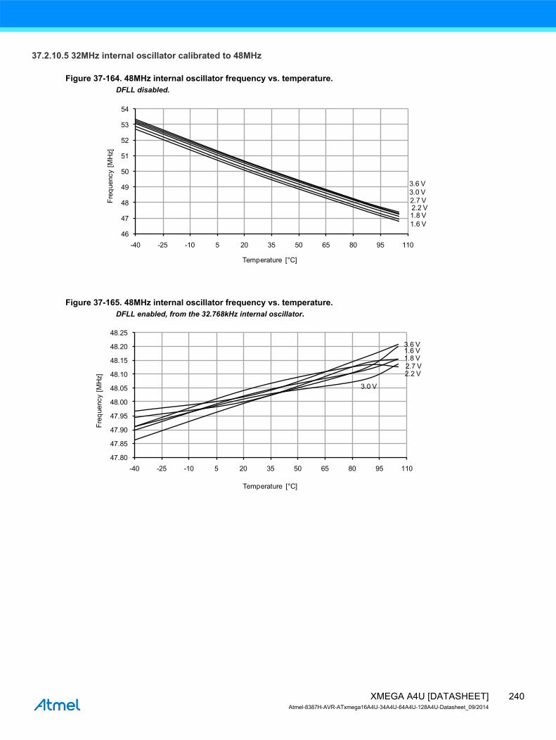
37.2.10.5 32MHz internal oscillator calibrated to 48MHz
Figure 37-164. 48MHz internal oscillator frequency vs. temperature.DFLL disabled.
Figure 37-165. 48MHz internal oscillator frequency vs. temperature.DFLL enabled, from the 32.768kHz internal oscillator.
3.6 V3.0 V2.7 V2.2 V1.8 V1.6 V
46
47
48
49
50
51
52
53
54
-40 -25 -10 5 20 35 50 65 80 95 110
Freq
uenc
y [M
Hz]
Temperature [°C]
3.6 V
3.0 V
2.7 V2.2 V
1.8 V1.6 V
47.80
47.85
47.90
47.95
48.00
48.05
48.10
48.15
48.20
48.25
-40 -25 -10 5 20 35 50 65 80 95 110
Freq
uenc
y [M
Hz]
Temperature [°C]
240XMEGA A4U [DATASHEET]Atmel-8387H-AVR-ATxmega16A4U-34A4U-64A4U-128A4U-Datasheet_09/2014

Figure 37-166. 48MHz internal oscillator CALA calibration step size.VCC = 3.0V.
37.2.11 Two-Wire Interface characteristics
Figure 37-167. SDA hold time vs. supply voltage.
105 °C85 °C25 °C-40 °C
0.10 %
0.13 %
0.16 %
0.19 %
0.22 %
0.25 %
0.28 %
0.31 %
0.34 %
0 16 32 48 64 80 96 112 128
Freq
uenc
y S
tep
size
[%]
CALA
105°C
85°C
25°C
- 40°C260
265
270
275
280
285
290
295
300
2.6 2.7 2.8 2.9 3.0 3.1 3.2 3.3 3.4 3.5 3.6
Hol
dtim
e [n
s]
Vcc [V]
241XMEGA A4U [DATASHEET]Atmel-8387H-AVR-ATxmega16A4U-34A4U-64A4U-128A4U-Datasheet_09/2014

37.2.12 PDI characteristics
Figure 37-168. Maximum PDI frequency vs. VCC.
105 °C
85 °C
25 °C
-40 °C
10
13
16
19
22
25
28
31
34
1.6 1.8 2 2.2 2.4 2.6 2.8 3 3.2 3.4 3.6
f MA
X[M
Hz]
VCC [V]
242XMEGA A4U [DATASHEET]Atmel-8387H-AVR-ATxmega16A4U-34A4U-64A4U-128A4U-Datasheet_09/2014

37.3 ATxmega64A4U
37.3.1 Current consumption
37.3.1.1 Active mode supply current
Figure 37-169. Active supply current vs. frequency.fSYS = 0 - 1MHz external clock, T = 25°C.
Figure 37-170. Active supply current vs. frequency.fSYS = 1 - 32MHz external clock, T = 25°C.
3.6V
3.0V
2.7V
2.2V
1.8V1.6V
0
100
200
300
400
500
600
700
0 0.1 0.2 0.3 0.4 0.5 0.6 0.7 0.8 0.9 1
I CC
[µA
]
Frequency [MHz]
3.6V
3.0V
2.7V
1.8V1.6V
0
2
4
6
8
10
12
0 4 8 12 16 20 24 28 32
I CC
[mA
]
Frequency [MHz]
2.2V
243XMEGA A4U [DATASHEET]Atmel-8387H-AVR-ATxmega16A4U-34A4U-64A4U-128A4U-Datasheet_09/2014

Figure 37-171. Active mode supply current vs. VCC.fSYS = 32.768kHz internal oscillator.
Figure 37-172. Active mode supply current vs. VCC.fSYS = 1MHz external clock.
105°C85°C25°C
- 40°C
50
70
90
110
130
150
170
190
210
230
250
1.6 1.8 2.0 2.2 2.4 2.6 2.8 3.0 3.2 3.4 3.6
I CC
[µA
]
VCC [V]
105°C85°C25°C
- 40°C
180
230
280
330
380
430
480
530
580
630
680
1.6 1.8 2.0 2.2 2.4 2.6 2.8 3.0 3.2 3.4 3.6
I CC
[µA
]
VCC [V]
244XMEGA A4U [DATASHEET]Atmel-8387H-AVR-ATxmega16A4U-34A4U-64A4U-128A4U-Datasheet_09/2014

Figure 37-173. Active mode supply current vs. VCC.fSYS = 2MHz internal oscillator.
Figure 37-174. Active mode supply current vs. VCC.fSYS = 32MHz internal oscillator prescaled to 8MHz.
105°C85°C25°C
- 40°C
400
500
600
700
800
900
1000
1100
1200
1300
1.6 1.8 2.0 2.2 2.4 2.6 2.8 3.0 3.2 3.4 3.6
I CC
[µA
]
VCC [V]
105°C85°C25°C
- 40°C
1.2
1.6
2.0
2.4
2.8
3.2
3.6
4.0
4.4
4.8
1.6 1.8 2.0 2.2 2.4 2.6 2.8 3.0 3.2 3.4 3.6
I CC
[mA
]
VCC [V]
245XMEGA A4U [DATASHEET]Atmel-8387H-AVR-ATxmega16A4U-34A4U-64A4U-128A4U-Datasheet_09/2014

Figure 37-175. Active mode supply current vs. VCC.fSYS = 32MHz internal oscillator.
37.3.1.2 Idle mode supply current
Figure 37-176. Idle mode supply current vs. frequency.fSYS = 0 - 1MHz external clock, T = 25°C.
105°C85°C25°C
- 40°C
7.0
7.5
8.0
8.5
9.0
9.5
10.0
10.5
11.0
11.5
12.0
2.7 2.8 2.9 3.0 3.1 3.2 3.3 3.4 3.5 3.6
I CC
[mA
]
VCC [V]
3.6 V
3.0 V
2.7 V
2.2 V
1.8 V1.6 V
0
15
30
45
60
75
90
105
120
135
150
0 0.1 0.2 0.3 0.4 0.5 0.6 0.7 0.8 0.9 1
I CC
[µA
]
Frequency [MHz]
246XMEGA A4U [DATASHEET]Atmel-8387H-AVR-ATxmega16A4U-34A4U-64A4U-128A4U-Datasheet_09/2014

Figure 37-177. Idle mode supply current vs. frequency.fSYS = 1 - 32MHz external clock, T = 25°C.
Figure 37-178. Idle mode supply current vs. VCC.fSYS = 32.768kHz internal oscillator.
3.6 V
3.0 V2.7 V
1.8 V1.6 V
0.0
0.5
1.0
1.5
2.0
2.5
3.0
3.5
4.0
4.5
0 4 8 12 16 20 24 28 32
I CC
[mA
]
F [MH ]
2.2 V
105°C
85°C25°C
- 40°C
28.00
28.75
29.50
30.25
31.00
31.75
32.50
33.25
34.00
34.75
1.6 1.8 2.0 2.2 2.4 2.6 2.8 3.0 3.2 3.4 3.6
I CC
[µA
]
VCC [V]
fSYS 32.768kHz Internal Oscillator
247XMEGA A4U [DATASHEET]Atmel-8387H-AVR-ATxmega16A4U-34A4U-64A4U-128A4U-Datasheet_09/2014

Figure 37-179. Idle mode supply current vs. VCC.fSYS = 1MHz external clock.
Figure 37-180. Idle mode supply current vs. VCC.fSYS = 2MHz internal oscillator.
105°C85°C25°C
- 40°C
45
57
69
81
93
105
117
129
141
153
1.6 1.8 2.0 2.2 2.4 2.6 2.8 3.0 3.2 3.4 3.6
I CC
[µA
]
VCC [V]
105°C85°C25°C
- 40°C
150
175
200
225
250
275
300
325
350
375
400
1.6 1.8 2.0 2.2 2.4 2.6 2.8 3.0 3.2 3.4 3.6
I CC
[µA
]
VCC [V]
248XMEGA A4U [DATASHEET]Atmel-8387H-AVR-ATxmega16A4U-34A4U-64A4U-128A4U-Datasheet_09/2014

Figure 37-181. Idle mode supply current vs. VCC.fSYS = 32MHz internal oscillator prescaled to 8MHz.
Figure 37-182. Idle mode current vs. VCC.fSYS = 32MHz internal oscillator.
105°C85°C25°C
- 40°C
650
800
950
1100
1250
1400
1550
1700
1850
1.6 1.8 2.0 2.2 2.4 2.6 2.8 3.0 3.2 3.4 3.6
I CC
[µA
]
VCC [V]
105°C85°C25°C
- 40°C
3.1
3.3
3.5
3.7
3.9
4.1
4.3
4.5
4.7
4.9
5.1
2.7 2.8 2.9 3.0 3.1 3.2 3.3 3.4 3.5 3.6
I CC
[mA
]
VCC [V]
249XMEGA A4U [DATASHEET]Atmel-8387H-AVR-ATxmega16A4U-34A4U-64A4U-128A4U-Datasheet_09/2014

37.3.1.3 Power-down mode supply current
Figure 37-183. Power-down mode supply current vs. temperature.All functions disabled.
Figure 37-184. Power-down mode supply current vs. VCC.All functions disabled.
3.6 V3.0 V2.7 V2.2 V1.8 V1.6 V
0.0
0.3
0.6
0.9
1.2
1.5
1.8
2.1
2.4
2.7
-45 -30 -15 0 15 30 45 60 75 90 105
I CC
[µA
]
Temperature [°C]
105°C
85°C
25°C- 40°C0.0
0.3
0.6
0.9
1.2
1.5
1.8
2.1
2.4
2.7
1.6 1.8 2.0 2.2 2.4 2.6 2.8 3.0 3.2 3.4 3.6
I CC
[µA
]
VCC [V]
250XMEGA A4U [DATASHEET]Atmel-8387H-AVR-ATxmega16A4U-34A4U-64A4U-128A4U-Datasheet_09/2014

Figure 37-185. Power-down mode supply current vs. VCC.Watchdog and sampled BOD enabled.
37.3.1.4 Power-save mode supply current
Figure 37-186. Power-save mode supply current vs.VCC.Real Time Counter enabled and running from 1.024kHz output of 32.768kHz TOSC.
105°C
85°C
25°C- 40°C
1.10
1.40
1.70
2.00
2.30
2.60
2.90
3.20
3.50
3.80
4.10
1.6 1.8 2.0 2.2 2.4 2.6 2.8 3.0 3.2 3.4 3.6
I CC
[µA
]
VCC [V]
Normal mode
Low-power mode
0
0.1
0.2
0.3
0.4
0.5
0.6
0.7
0.8
0.9
VCC [V]
I CC
[µA
]
1.6 1.8 2.0 2.2 2.4 2.6 2.8 3.0 3.2 3.4 3.6
251XMEGA A4U [DATASHEET]Atmel-8387H-AVR-ATxmega16A4U-34A4U-64A4U-128A4U-Datasheet_09/2014

37.3.1.5 Standby mode supply current
Figure 37-187. Standby supply current vs. VCC.Standby, fSYS = 1MHz.
Figure 37-188. Standby supply current vs. VCC.25°C, running from different crystal oscillators.
105 °C
85 °C
25 °C-40 °C
2.5
3.5
4.5
5.5
6.5
7.5
8.5
9.5
10.5
11.5
12.5
1.6 1.8 2 2.2 2.4 2.6 2.8 3 3.2 3.4 3.6
I CC
[uA
]
VCC [V]
16MHz12MHz
8MHz
2MHz
0.454MHz
160
200
240
280
320
360
400
440
480
1.6 1.8 2 2.2 2.4 2.6 2.8 3 3.2 3.4 3.6
VCC [V]
ICC [
µA
]
252XMEGA A4U [DATASHEET]Atmel-8387H-AVR-ATxmega16A4U-34A4U-64A4U-128A4U-Datasheet_09/2014

37.3.2 I/O Pin Characteristics
37.3.2.1 Pull-up
Figure 37-189. I/O pin pull-up resistor current vs. input voltage.VCC = 1.8V.
Figure 37-190. I/O pin pull-up resistor current vs. input voltage.VCC = 3.0V.
105°C85°C25°C
- 40°C
0
10
20
30
40
50
60
70
0.0 0.2 0.4 0.6 0.8 1.0 1.2 1.4 1.6 1.8
I PIN
[uA
]
VPIN [V]
105°C85°C25°C
- 40°C
0
15
30
45
60
75
90
105
120
0.0 0.3 0.6 0.9 1.2 1.5 1.8 2.1 2.4 2.7 3.0
I PIN
[µA
]
VPIN [V]
253XMEGA A4U [DATASHEET]Atmel-8387H-AVR-ATxmega16A4U-34A4U-64A4U-128A4U-Datasheet_09/2014

Figure 37-191. I/O pin pull-up resistor current vs. input voltage.VCC = 3.3V.
37.3.2.2 Output Voltage vs. Sink/Source Current
Figure 37-192. I/O pin output voltage vs. source current.VCC = 1.8V.
105°C85°C25°C
- 40°C
0
15
30
45
60
75
90
105
120
135
0.0 0.3 0.6 0.9 1.2 1.5 1.8 2.1 2.4 2.7 3.0 3.3
I PIN
[µA
]
VPIN [V]
105°C85°C
25°C
- 40°C
0.5
0.7
0.9
1.1
1.3
1.5
1.7
1.9
-9 -8 -7 -6 -5 -4 -3 -2 -1 0
VP
IN[V
]
IPIN [mA]
254XMEGA A4U [DATASHEET]Atmel-8387H-AVR-ATxmega16A4U-34A4U-64A4U-128A4U-Datasheet_09/2014

Figure 37-193. I/O pin output voltage vs. source current.VCC = 3.0V.
Figure 37-194. I/O pin output voltage vs. source current.VCC = 3.3V.
105°C85°C25°C
- 40°C
0.0
0.4
0.8
1.2
1.6
2.0
2.4
2.8
3.2
-30 -27 -24 -21 -18 -15 -12 -9 -6 -3 0
VP
IN[V
]
IPIN [mA]
105°C
85°C
25°C
- 40°C
0.0
0.4
0.8
1.2
1.6
2.0
2.4
2.8
3.2
3.6
-30 -27 -24 -21 -18 -15 -12 -9 -6 -3 0
VP
IN[V
]
IPIN [mA]
255XMEGA A4U [DATASHEET]Atmel-8387H-AVR-ATxmega16A4U-34A4U-64A4U-128A4U-Datasheet_09/2014
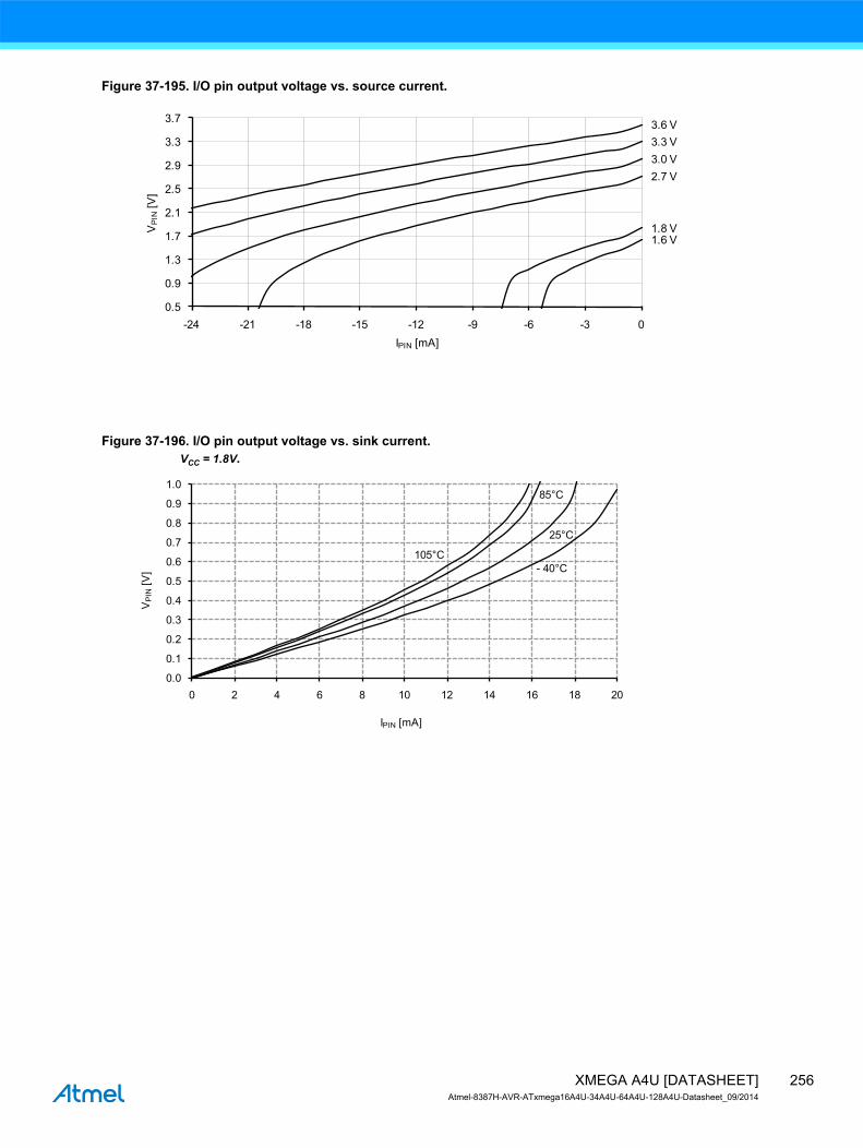
Figure 37-195. I/O pin output voltage vs. source current.
Figure 37-196. I/O pin output voltage vs. sink current.VCC = 1.8V.
3.6 V3.3 V3.0 V2.7 V
1.8 V1.6 V
0.5
0.9
1.3
1.7
2.1
2.5
2.9
3.3
3.7
-24 -21 -18 -15 -12 -9 -6 -3 0
VP
IN[V
]
IPIN [mA]
- 40°C
0.0
0.1
0.2
0.3
0.4
0.5
0.6
0.7
0.8
0.9
1.0
0 2 4 6 8 10 12 14 16 18 20
VP
IN[V
]
IPIN [mA]
25°C
85°C
105°C
256XMEGA A4U [DATASHEET]Atmel-8387H-AVR-ATxmega16A4U-34A4U-64A4U-128A4U-Datasheet_09/2014

Figure 37-197. I/O pin output voltage vs. sink current.VCC = 3.0V.
Figure 37-198. I/O pin output voltage vs. sink current.VCC = 3.3V.
105°C85°C
25°C- 40°C
0.0
0.1
0.2
0.3
0.4
0.5
0.6
0.7
0.8
0.9
1.0
0 3 6 9 12 15 18 21 24 27 30
VP
IN[V
]
IPIN [mA]
105°C85°C
25°C- 40°C
0.0
0.1
0.2
0.3
0.4
0.5
0.6
0.7
0.8
0.9
1.0
0 3 6 9 12 15 18 21 24 27 30
VP
IN[V
]
IPIN [mA]
257XMEGA A4U [DATASHEET]Atmel-8387H-AVR-ATxmega16A4U-34A4U-64A4U-128A4U-Datasheet_09/2014

Figure 37-199. I/O pin output voltage vs. sink current.
37.3.2.3 Thresholds and Hysteresis
Figure 37-200. I/O pin input threshold voltage vs. VCC.T = 25°C.
3.6 V3.3 V3.0 V2.7 V
0.00
0.15
0.30
0.45
0.60
0.75
0.90
1.05
1.20
1.35
1.50
0 3 6 9 12 15 18 21 24 27 30
VP
IN[V
]
IPIN [mA]
1.6 V 1.8 V
VIL
VIH
0.0
0.2
0.4
0.6
0.8
1.0
1.2
1.4
1.6
1.8
1.6 1.8 2 2.2 2.4 2.6 2.8 3 3.2 3.4 3.6
Vcc [V]
Vth
reshold
[V
]
258XMEGA A4U [DATASHEET]Atmel-8387H-AVR-ATxmega16A4U-34A4U-64A4U-128A4U-Datasheet_09/2014

Figure 37-201. I/O pin input threshold voltage vs. VCC.VIH I/O pin read as “1”.
Figure 37-202. I/O pin input threshold voltage vs. VCC.VIL I/O pin read as “0”.
105 °C85 °C25 °C
-40 °C
0.8
0.9
1.0
1.1
1.2
1.3
1.4
1.5
1.6
1.7
1.8
1.6 1.8 2.0 2.2 2.4 2.6 2.8 3.0 3.2 3.4 3.6
Vth
resh
old
[V]
VCC [V]
105 °C85 °C25 °C
-40 °C
0.55
0.70
0.85
1.00
1.15
1.30
1.45
1.60
1.75
1.6 1.8 2.0 2.2 2.4 2.6 2.8 3.0 3.2 3.4 3.6
Vth
resh
old
[V]
VCC [V]
259XMEGA A4U [DATASHEET]Atmel-8387H-AVR-ATxmega16A4U-34A4U-64A4U-128A4U-Datasheet_09/2014

Figure 37-203. I/O pin input hysteresis vs. VCC.
37.3.3 ADC Characteristics
Figure 37-204. INL error vs. external VREF.T = 25°C, VCC = 3.6V, external reference.
105 °C
85 °C
25 °C -40 °C
0.08
0.11
0.14
0.17
0.20
0.23
0.26
0.29
0.32
1.6 1.8 2.0 2.2 2.4 2.6 2.8 3.0 3.2 3.4 3.6
Vth
resh
old
[V]
VCC [V]
Single-ended unsigned mode
Single-ended signed mode
Dif ferential mode
0.0
0.3
0.6
0.9
1.2
1.5
1.8
2.1
2.4
2.7
1.0 1.2 1.4 1.6 1.8 2.0 2.2 2.4 2.6 2.8 3.0
INL
[LSB
]
Vref [V]
260XMEGA A4U [DATASHEET]Atmel-8387H-AVR-ATxmega16A4U-34A4U-64A4U-128A4U-Datasheet_09/2014

Figure 37-205. INL error vs. sample rate.T = 25°C, VCC = 2.7V, VREF = 1.0V external.
Figure 37-206. INL error vs. input code
Single-ended signed mode
Single-ended signed mode
Dif ferential mode
0.0
0.2
0.4
0.6
0.8
1.0
1.2
1.4
1.6
500 650 800 950 1100 1250 1400 1550 1700 1850 2000
INL
[LSB
]
ADC sample rate [kSps]
0 512 1024 1536 2048 2560 3072 3584 4096
2.0
1.5
1.0
0.5
0.0
-0.5
-1.0
-1.5
-2.0
INL
[LSB]
ADC input code
261XMEGA A4U [DATASHEET]Atmel-8387H-AVR-ATxmega16A4U-34A4U-64A4U-128A4U-Datasheet_09/2014

Figure 37-207. DNL error vs. external VREF.T = 25°C, VCC = 3.6V, external reference.
Figure 37-208. DNL error vs. sample rate.T = 25°C, VCC = 2.7V, VREF = 1.0V external.
Single-ended unsigned mode
Single-ended signed mode
Dif ferential mode
0.2
0.3
0.4
0.5
0.6
0.7
0.8
0.9
1.0
1.1
1.0 1.2 1.4 1.6 1.8 2.0 2.2 2.4 2.6 2.8 3.0
DN
L [L
SB]
Vref [V]
Single-ended unsigned mode
Single-ended signed mode
Dif ferential mode
0.23
0.26
0.28
0.31
0.33
0.36
0.38
0.41
0.43
500 650 800 950 1100 1250 1400 1550 1700 1850 2000
DN
L [L
SB]
ADC sample rate [kSps]
262XMEGA A4U [DATASHEET]Atmel-8387H-AVR-ATxmega16A4U-34A4U-64A4U-128A4U-Datasheet_09/2014

Figure 37-209. DNL error vs. input code.
Figure 37-210. Gain error vs. VREF.T = 25°C, VCC = 3.6V, ADC sampling speed = 500ksps.
0 512 1024 1536 2048 2560 3072 3584 4096
1.0
0.8
0.6
0.4
0.2
0.0
-0.2
-0.4
-0.6
-0.8
-1.0
DN
L [L
SB]
ADC input code
Single-ended unsigned mode
Single-ended signed mode
Dif ferential mode
0
2
4
6
8
10
12
1.0 1.2 1.4 1.6 1.8 2.0 2.2 2.4 2.6 2.8 3.0
Gai
n Er
ror [
mV]
Vref [V]
263XMEGA A4U [DATASHEET]Atmel-8387H-AVR-ATxmega16A4U-34A4U-64A4U-128A4U-Datasheet_09/2014

Figure 37-211. Gain error vs. VCC.T = 25°C, VREF = external 1.0V, ADC sampling speed = 500ksps.
Figure 37-212. Offset error vs. VREF.T = 25°C, VCC = 3.6V, ADC sampling speed = 500ksps.
Single-ended unsigned mode
Single-ended signed mode
Dif ferential mode
0
1
2
3
4
5
6
7
1.6 1.8 2.0 2.2 2.4 2.6 2.8 3.0 3.2 3.4 3.6
Gai
n Er
ror [
mV]
Vcc [V]
Dif ferential mode
-1.5
-1.5
-1.4
-1.4
-1.3
-1.3
-1.2
-1.2
-1.1
-1.1
-1.0
1.0 1.2 1.4 1.6 1.8 2.0 2.2 2.4 2.6 2.8 3.0
Offs
et E
rror
[mV]
Vref [V]
264XMEGA A4U [DATASHEET]Atmel-8387H-AVR-ATxmega16A4U-34A4U-64A4U-128A4U-Datasheet_09/2014

Figure 37-213. Gain error vs. temperature.VCC = 2.7V, VREF = external 1.0V.
Figure 37-214. Offset error vs. VCC.T = 25°C, VREF = external 1.0V, ADC sampling speed = 500ksps.
Single-ended unsigned mode
Single-ended signed mode
Dif ferential mode
0
1
2
3
4
5
6
7
8
-45 -35 -25 -15 -5 5 15 25 35 45 55 65 75 85 95 105
Gai
n Er
ror [
mV]
Temperature [oC]
Dif ferential mode
-1.1
-1.0
-0.9
-0.8
-0.7
-0.6
-0.5
-0.4
-0.3
1.6 1.8 2.0 2.2 2.4 2.6 2.8 3.0 3.2 3.4 3.6
Offs
et E
rror
[mV]
Vcc [V]
265XMEGA A4U [DATASHEET]Atmel-8387H-AVR-ATxmega16A4U-34A4U-64A4U-128A4U-Datasheet_09/2014

Figure 37-215. Noise vs. VREF.T = 25°C, VCC = 3.6V, ADC sampling speed = 500ksps.
Figure 37-216. Noise vs. VCC.T = 25°C, VREF = external 1.0V, ADC sampling speed = 500ksps.
Single-ended unsigend mode
Single-ended signed mode
Dif ferential mode
0.0
0.1
0.2
0.3
0.4
0.5
0.6
0.7
0.8
0.9
1.0 1.2 1.4 1.6 1.8 2.0 2.2 2.4 2.6 2.8 3.0
Noi
se [m
V R
MS]
Vref [V]
Single-ended unsigned mode
Single-ended signed mode
Dif ferential mode
0.0
0.1
0.2
0.3
0.4
0.5
0.6
0.7
0.8
1.6 1.8 2.0 2.2 2.4 2.6 2.8 3.0 3.2 3.4 3.6
Noi
se [m
V R
MS]
Vcc [V]
266XMEGA A4U [DATASHEET]Atmel-8387H-AVR-ATxmega16A4U-34A4U-64A4U-128A4U-Datasheet_09/2014

37.3.4 DAC Characteristics
Figure 37-217. DAC INL error vs. VREF.VCC = 3.6V.
Figure 37-218. DNL error vs. VREF.VCC = 3.6V.
105°C85°C25°C
- 40°C
0.0
0.3
0.6
0.9
1.2
1.5
1.8
2.1
2.4
1.0 1.2 1.4 1.6 1.8 2.0 2.2 2.4 2.6 2.8 3.0
DAC
INL
[LSB
]
Vref [V]
105°C85°C25°C
- 40°C
0.0
0.2
0.4
0.6
0.8
1.0
1.2
1.4
1.6
1.8
1.0 1.2 1.4 1.6 1.8 2.0 2.2 2.4 2.6 2.8 3.0
DAC
DN
L [L
SB]
Vref [V]
267XMEGA A4U [DATASHEET]Atmel-8387H-AVR-ATxmega16A4U-34A4U-64A4U-128A4U-Datasheet_09/2014
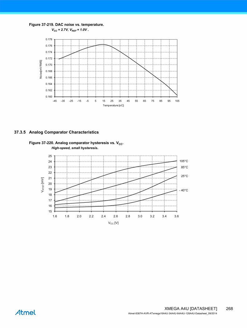
Figure 37-219. DAC noise vs. temperature.VCC = 2.7V, VREF = 1.0V .
37.3.5 Analog Comparator Characteristics
Figure 37-220. Analog comparator hysteresis vs. VCC.High-speed, small hysteresis.
0.160
0.162
0.164
0.166
0.168
0.170
0.172
0.174
0.176
0.178
-45 -35 -25 -15 -5 5 15 25 35 45 55 65 75 85 95 105
Noi
se[m
V R
MS]
Temperature [oC]
105°C
85°C
25°C
- 40°C
15
16
17
18
19
20
21
22
23
24
25
1.6 1.8 2.0 2.2 2.4 2.6 2.8 3.0 3.2 3.4 3.6
VH
YS
T[m
V]
VCC [V]
268XMEGA A4U [DATASHEET]Atmel-8387H-AVR-ATxmega16A4U-34A4U-64A4U-128A4U-Datasheet_09/2014

Figure 37-221. Analog comparator hysteresis vs. VCC.Low power, small hysteresis.
Figure 37-222. Analog comparator hysteresis vs. VCC.High-speed mode, large hysteresis.
105°C85°C
25°C
- 40°C
20
22
24
26
28
30
32
34
36
1.6 1.8 2.0 2.2 2.4 2.6 2.8 3.0 3.2 3.4 3.6
VH
YS
T[m
V]
VCC [V]
105°C85°C
25°C
- 40°C
27
29
31
33
35
37
39
41
43
45
47
1.6 1.8 2 2.2 2.4 2.6 2.8 3 3.2 3.4 3.6
VH
YS
T[m
V]
VCC [V]
269XMEGA A4U [DATASHEET]Atmel-8387H-AVR-ATxmega16A4U-34A4U-64A4U-128A4U-Datasheet_09/2014

Figure 37-223. Analog comparator hysteresis vs. VCC.Low power, large hysteresis.
Figure 37-224. Analog comparator current source vs. calibration value.Temperature = 25°C.
105°C85°C
25°C
- 40°C
46
49
52
55
58
61
64
67
70
73
76
1.6 1.8 2.0 2.2 2.4 2.6 2.8 3.0 3.2 3.4 3.6
VH
YS
T[m
V]
VCC [V]
2
3
4
5
6
7
8
0 1 2 3 4 5 6 7 8 9 10 11 12 13 14 15
I CU
RR
EN
TSO
UR
CE
[µA
]
CURRCALIBA[3..0]
3.6V3.0V2.7V2.2V1.8V1.6V
270XMEGA A4U [DATASHEET]Atmel-8387H-AVR-ATxmega16A4U-34A4U-64A4U-128A4U-Datasheet_09/2014

Figure 37-225. Analog comparator current source vs. calibration value.VCC = 3.0V.
Figure 37-226. Voltage scaler INL vs. SCALEFAC.T = 25°C, VCC = 3.0V.
105°C85°C25°C
- 40°C
3.6
4.0
4.4
4.8
5.2
5.6
6.0
6.4
6.8
7.2
0 1 2 3 4 5 6 7 8 9 10 11 12 13 14 15
I CU
RR
EN
TSO
UR
CE
[uA
]
CURRCALIBA[3..0]
-0.15
-0.12
-0.09
-0.06
-0.03
0.00
0.03
0.06
0.09
0.12
0.15
0 8 16 24 32 40 48 56 64
INL
[LS
B]
SCALEFAC
271XMEGA A4U [DATASHEET]Atmel-8387H-AVR-ATxmega16A4U-34A4U-64A4U-128A4U-Datasheet_09/2014

37.3.6 Internal 1.0V reference Characteristics
Figure 37-227. ADC/DAC Internal 1.0V reference vs. temperature.
37.3.7 BOD Characteristics
Figure 37-228. BOD thresholds vs. temperature.BOD level = 1.6V.
3.6 V3.0 V2.7 V2.2 V1.8 V1.6 V
0.992
0.994
0.996
0.998
1.000
1.002
1.004
-45 -30 -15 0 15 30 45 60 75 90 105
Ban
dgap
Vol
tage
[V]
Temperature [°C]
Rising Vcc
Falling Vcc
1.617
1.620
1.623
1.626
1.629
1.632
1.635
1.638
1.641
1.644
-45 -30 -15 0 15 30 45 60 75 90 105
VB
OT
[V]
Temperature [°C]
272XMEGA A4U [DATASHEET]Atmel-8387H-AVR-ATxmega16A4U-34A4U-64A4U-128A4U-Datasheet_09/2014

Figure 37-229. BOD thresholds vs. temperature.BOD level = 3.0V.
37.3.8 External Reset Characteristics
Figure 37-230. Minimum Reset pin pulse width vs. VCC.
Rising Vcc
Falling Vcc
3.00
3.01
3.02
3.03
3.04
3.05
3.06
3.07
3.08
-45 -30 -15 0 15 30 45 60 75 90 105
VB
OT
[V]
Temperature [°C]
105°C85°C25°C
- 40°C85
90
95
100
105
110
115
120
125
130
135
1.6 1.8 2.0 2.2 2.4 2.6 2.8 3.0 3.2 3.4 3.6
t RS
T[n
s]
VCC [V]
273XMEGA A4U [DATASHEET]Atmel-8387H-AVR-ATxmega16A4U-34A4U-64A4U-128A4U-Datasheet_09/2014

Figure 37-231. Reset pin pull-up resistor current vs. reset pin voltage.VCC = 1.8V.
Figure 37-232. Reset pin pull-up resistor current vs. reset pin voltage.VCC = 3.0V.
105°C85°C25°C
- 40°C
0
10
20
30
40
50
60
70
80
0.0 0.2 0.4 0.6 0.8 1.0 1.2 1.4 1.6 1.8
I RE
SE
T[µ
A]
VRESET [V]
105°C85°C25°C
- 40°C
0
15
30
45
60
75
90
105
120
0.0 0.3 0.6 0.9 1.2 1.5 1.8 2.1 2.4 2.7 3.0
I RE
SE
T[µ
A]
VRESET [V]
274XMEGA A4U [DATASHEET]Atmel-8387H-AVR-ATxmega16A4U-34A4U-64A4U-128A4U-Datasheet_09/2014

Figure 37-233. Reset pin pull-up resistor current vs. reset pin voltage.VCC = 3.3V.
Figure 37-234. Reset pin input threshold voltage vs. VCC.VIH - Reset pin read as “1”.
105°C85°C25°C
- 40°C
0
15
30
45
60
75
90
105
120
135
150
0.0 0.3 0.6 0.9 1.2 1.5 1.8 2.1 2.4 2.7 3.0 3.3
I RE
SE
T[µ
A]
VRESET [V]
105°C85°C25°C
-
- 40°C
1.0
1.2
1.3
1.5
1.6
1.8
1.9
2.1
2.2
1.6 1.8 2.0 2.2 2.4 2.6 2.8 3.0 3.2 3.4 3.6
VTH
RE
SH
OLD
[V]
VCC [V]
275XMEGA A4U [DATASHEET]Atmel-8387H-AVR-ATxmega16A4U-34A4U-64A4U-128A4U-Datasheet_09/2014

Figure 37-235. Reset pin input threshold voltage vs. VCC.VIL - Reset pin read as “0”.
37.3.9 Power-on Reset Characteristics
Figure 37-236. Power-on reset current consumption vs. VCC.BOD level = 3.0V, enabled in continuous mode.
105°C85°C25°C
- 40°C
0.40
0.55
0.70
0.85
1.00
1.15
1.30
1.45
1.60
1.75
1.6 1.8 2.0 2.2 2.4 2.6 2.8 3.0 3.2 3.4 3.6
VTH
RE
SH
OLD
[V]
VCC [V]
105°C85°C25°C
- 40°C
0
50
100
150
200
250
300
0.4 0.7 1.0 1.3 1.6 1.9 2.2 2.5 2.8
I CC
[µA
]
VCC [V]
276XMEGA A4U [DATASHEET]Atmel-8387H-AVR-ATxmega16A4U-34A4U-64A4U-128A4U-Datasheet_09/2014

Figure 37-237. Power-on reset current consumption vs. VCC.BOD level = 3.0V, enabled in sampled mode.
37.3.10 Oscillator Characteristics
37.3.10.1 Ultra Low-Power internal oscillator
Figure 37-238. Ultra Low-Power internal oscillator frequency vs. temperature.
105°C
85°C25°C
- 40°C
0
50
100
150
200
250
300
0.4 0.7 1.0 1.3 1.6 1.9 2.2 2.5 2.8
I CC
[µA
]
VCC [V]
3.6 V3.0 V2.7 V2.2 V1.8 V1.6 V31.0
31.3
31.6
31.9
32.2
32.5
32.8
33.1
33.4
33.7
34.0
-45 -30 -15 0 15 30 45 60 75 90 105
Freq
uenc
y [k
Hz]
Temperature [°C]
277XMEGA A4U [DATASHEET]Atmel-8387H-AVR-ATxmega16A4U-34A4U-64A4U-128A4U-Datasheet_09/2014

37.3.10.2 32.768kHz Internal Oscillator
Figure 37-239. 32.768kHz internal oscillator frequency vs. temperature.
Figure 37-240. 32.768kHz internal oscillator frequency vs. calibration value.VCC = 3.0V, T = 25°C.
3.6 V3.0 V2.7 V2.2 V1.8 V1.6 V
32.55
32.58
32.61
32.64
32.67
32.70
32.73
32.76
32.79
32.82
32.85
-45 -30 -15 0 15 30 45 60 75 90 105
Freq
uenc
y [k
Hz]
Temperature [°C]
23
26
29
32
35
38
41
44
47
50
53
0 30 60 90 120 150 180 210 240 270
Freq
uenc
y [k
Hz]
RC32KCAL[7..0]
278XMEGA A4U [DATASHEET]Atmel-8387H-AVR-ATxmega16A4U-34A4U-64A4U-128A4U-Datasheet_09/2014

37.3.10.3 2MHz Internal Oscillator
Figure 37-241. 2MHz internal oscillator frequency vs. temperature.DFLL disabled.
Figure 37-242. 2MHz internal oscillator frequency vs. temperature.DFLL enabled, from the 32.768kHz internal oscillator .
3.6 V3.0 V2.7 V2.2 V1.8 V1.6 V
1.94
1.96
1.98
2.00
2.02
2.04
2.06
2.08
2.10
2.12
-45 -30 -15 0 15 30 45 60 75 90 105
Freq
uenc
y [M
Hz]
Temperature [°C]
3.6 V
3.0 V
2.7 V
2.2 V1.8 V
1.6 V
1.9881.9901.9921.9941.9961.9982.0002.0022.0042.0062.0082.010
-45 -30 -15 0 15 30 45 60 75 90 105
Freq
uenc
y [M
Hz]
Temperature [°C]
279XMEGA A4U [DATASHEET]Atmel-8387H-AVR-ATxmega16A4U-34A4U-64A4U-128A4U-Datasheet_09/2014

Figure 37-243. 2MHz internal oscillator CALA calibration step size.VCC = 3V.
37.3.10.4 32MHz Internal Oscillator
Figure 37-244. 32MHz internal oscillator frequency vs. temperature.DFLL disabled.
105°C85°C
25°C- 40°C
0.12 %
0.14 %
0.16 %
0.18 %
0.20 %
0.22 %
0.24 %
0.26 %
0.28 %
0 16 32 48 64 80 96 112 128
Freq
uenc
y S
tep
size
[%]
CALA
3.6 V3.0 V2.7 V2.2 V1.8 V1.6 V
31.0
31.5
32.0
32.5
33.0
33.5
34.0
34.5
35.0
35.5
-45 -30 -15 0 15 30 45 60 75 90 105
Freq
uenc
y [M
Hz]
Temperature [°C]
280XMEGA A4U [DATASHEET]Atmel-8387H-AVR-ATxmega16A4U-34A4U-64A4U-128A4U-Datasheet_09/2014

Figure 37-245. 32MHz internal oscillator frequency vs. temperature.DFLL enabled, from the 32.768kHz internal oscillator.
Figure 37-246. 32MHz internal oscillator CALA calibration step size.VCC = 3.0V.
3.6 V
3.0 V
2.7 V2.2 V1.8 V 1.6 V
31.80
31.84
31.88
31.92
31.96
32.00
32.04
32.08
32.12
-45 -30 -15 0 15 30 45 60 75 90 105
Freq
uenc
y [M
Hz]
Temperature [°C]
105°C85°C
25°C
- 40°C
0.10 %
0.13 %
0.16 %
0.19 %
0.22 %
0.25 %
0.28 %
0.31 %
0.34 %
0 15 30 45 60 75 90 105 120 135
Freq
uenc
y S
tep
size
[%]
CALA
281XMEGA A4U [DATASHEET]Atmel-8387H-AVR-ATxmega16A4U-34A4U-64A4U-128A4U-Datasheet_09/2014

Figure 37-247. 32MHz internal oscillator CALB calibration step size.VCC = 3.0V
37.3.10.5 32MHz internal oscillator calibrated to 48MHz
Figure 37-248. 48MHz internal oscillator frequency vs. temperature.DFLL disabled.
105°C85°C25°C
- 40°C
0.80 %
1.00 %
1.20 %
1.40 %
1.60 %
1.80 %
2.00 %
2.20 %
2.40 %
2.60 %
2.80 %
0 8 16 24 32 40 48 56 64
Freq
uenc
y S
tep
size
[%]
CALB
3.6 V3.0 V2.7 V2.2 V1.8 V1.6 V46.2
47.0
47.8
48.6
49.4
50.2
51.0
51.8
52.6
53.4
-45 -30 -15 0 15 30 45 60 75 90 105
Freq
uenc
y[M
Hz]
Temperature [°C]
282XMEGA A4U [DATASHEET]Atmel-8387H-AVR-ATxmega16A4U-34A4U-64A4U-128A4U-Datasheet_09/2014

Figure 37-249. 48MHz internal oscillator frequency vs. temperature.DFLL enabled, from the 32.768kHz internal oscillator.
Figure 37-250. 48MHz internal oscillator CALA calibration step size.VCC = 3.0V
3.6 V3.0 V2.7 V2.2 V1.8 V1.6 V
47.70
47.75
47.80
47.85
47.90
47.95
48.00
48.05
48.10
48.15
-45 -30 -15 0 15 30 45 60 75 90 105
Freq
uenc
y[M
Hz]
Temperature [°C]
105°C
85°C25°C
- 40°C
0.10 %
0.12 %
0.14 %
0.16 %
0.18 %
0.20 %
0.22 %
0.24 %
0.26 %
0.28 %
0.30 %
0 16 32 48 64 80 96 112 128
Freq
uenc
y S
tep
size
[%]
CALA
283XMEGA A4U [DATASHEET]Atmel-8387H-AVR-ATxmega16A4U-34A4U-64A4U-128A4U-Datasheet_09/2014

37.3.11 Two-Wire Interface characteristics
Figure 37-251. SDA hold time vs. supply voltage.
37.3.12 PDI characteristics
Figure 37-252. Maximum PDI frequency vs. VCC.
105°C
85°C
25°C
- 40°C260
265
270
275
280
285
290
295
300
2.6 2.7 2.8 2.9 3.0 3.1 3.2 3.3 3.4 3.5 3.6
Hol
dtim
e [n
s]
Vcc [V]
105°C
85°C25°C
-
- 40°C
10
12
14
16
18
20
22
24
26
28
30
1.6 1.8 2.0 2.2 2.4 2.6 2.8 3.0 3.2 3.4 3.6
Max
imum
Fre
quen
cy [
MH
z]
VCC [V]
284XMEGA A4U [DATASHEET]Atmel-8387H-AVR-ATxmega16A4U-34A4U-64A4U-128A4U-Datasheet_09/2014

37.4 ATxmega128A4U
37.4.1 Current consumption
37.4.1.1 Active mode supply current
Figure 37-253. Active supply current vs. frequency.fSYS = 0 - 1MHz external clock, T = 25°C.
Figure 37-254. Active supply current vs. frequency.fSYS = 1 - 32MHz external clock, T = 25°C.
3.6V
3.0V
2.7V
2.2V
1.8V1.6V
0
100
200
300
400
500
600
700
800
0 0.1 0.2 0.3 0.4 0.5 0.6 0.7 0.8 0.9 1
Frequency [MHz]
Icc [µA
]
3.6V
3.0V
2.7V
0
1.5
3.0
4.5
6.0
7.5
9.0
10.5
12.0
13.5
0 4 8 12 16 20 24 28 32
Frequency [MHz]
Icc [m
A]
2.2V
1.8V
285XMEGA A4U [DATASHEET]Atmel-8387H-AVR-ATxmega16A4U-34A4U-64A4U-128A4U-Datasheet_09/2014

Figure 37-255. Active mode supply current vs. VCC.fSYS = 32.768kHz internal oscillator
Figure 37-256. Active mode supply current vs. VCC.fSYS = 1MHz external clock.
105 °C85 °C25 °C
- 40 °C
0
30
60
90
120
150
180
210
240
270
1.6 1.8 2.0 2.2 2.4 2.6 2.8 3.0 3.2 3.4 3.6
IccV
cc [u
A]
VCC [V]
105 °C85 °C25 °C-40 °C
0
100
200
300
400
500
600
700
800
1.6 1.8 2.0 2.2 2.4 2.6 2.8 3.0 3.2 3.4 3.6
Icc
[uA]
Vcc [V]
286XMEGA A4U [DATASHEET]Atmel-8387H-AVR-ATxmega16A4U-34A4U-64A4U-128A4U-Datasheet_09/2014

Figure 37-257. Active mode supply current vs. VCC.fSYS = 2MHz internal oscillator
Figure 37-258. Active mode supply current vs. VCC.fSYS = 32MHz internal oscillator prescaled to 8MHz.
105 °C85 °C25 °C-40 °C
0
175
350
525
700
875
1050
1225
1400
1.6 1.8 2 2.2 2.4 2.6 2.8 3 3.2 3.4 3.6
Icc
[uA]
Vcc [V]
105 °C85 °C25 °C-40 °C
1000
1600
2200
2800
3400
4000
4600
5200
5800
1.6 1.8 2.0 2.2 2.4 2.6 2.8 3.0 3.2 3.4 3.6
Icc
[uA]
VCC [V]
287XMEGA A4U [DATASHEET]Atmel-8387H-AVR-ATxmega16A4U-34A4U-64A4U-128A4U-Datasheet_09/2014
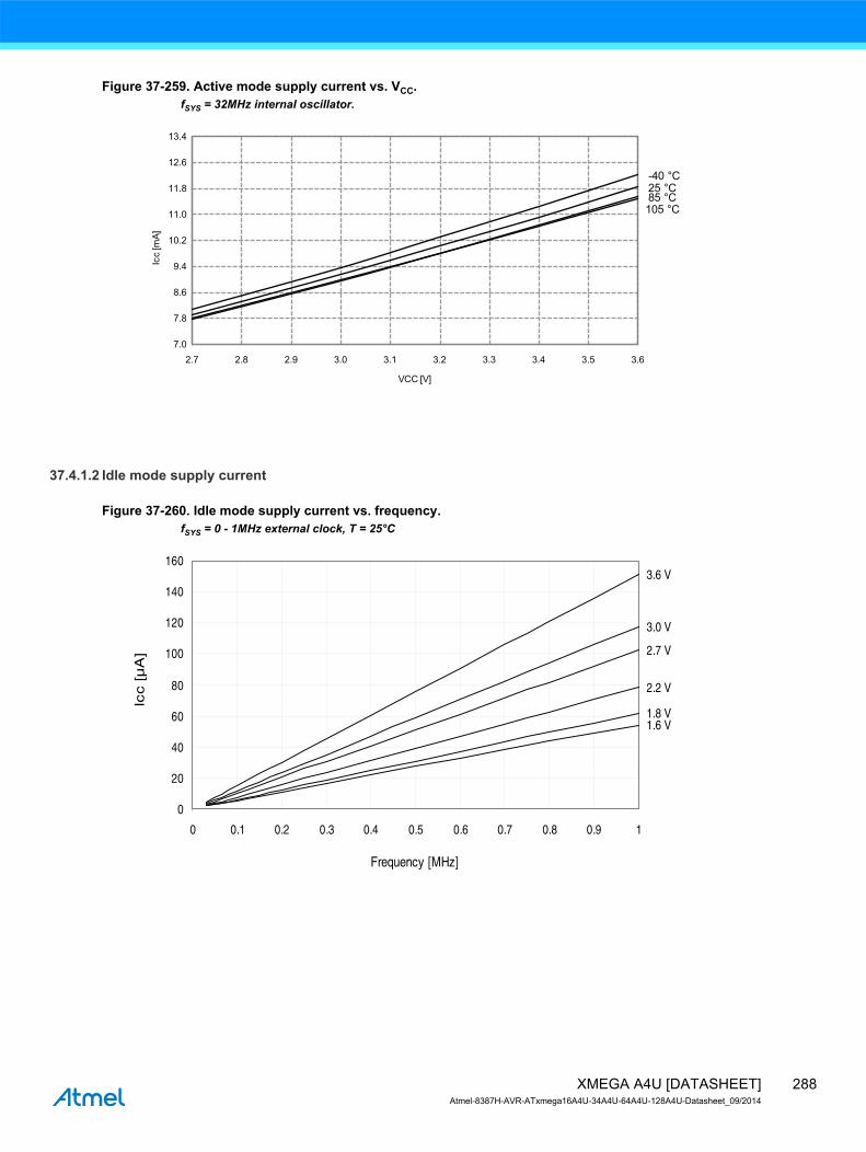
Figure 37-259. Active mode supply current vs. VCC.fSYS = 32MHz internal oscillator.
37.4.1.2 Idle mode supply current
Figure 37-260. Idle mode supply current vs. frequency.fSYS = 0 - 1MHz external clock, T = 25°C
105 °C85 °C25 °C-40 °C
7.0
7.8
8.6
9.4
10.2
11.0
11.8
12.6
13.4
2.7 2.8 2.9 3.0 3.1 3.2 3.3 3.4 3.5 3.6
Icc
[mA]
VCC [V]
3.6 V
3.0 V
2.7 V
2.2 V
1.8 V1.6 V
0
20
40
60
80
100
120
140
160
0 0.1 0.2 0.3 0.4 0.5 0.6 0.7 0.8 0.9 1
Frequency [MHz]
Icc [µ
A]
288XMEGA A4U [DATASHEET]Atmel-8387H-AVR-ATxmega16A4U-34A4U-64A4U-128A4U-Datasheet_09/2014

Figure 37-261. Idle mode supply current vs. frequency.fSYS = 1 - 32MHz external clock, T = 25°C
Figure 37-262. Idle mode supply current vs. VCC.fSYS = 32.768kHz internal oscillator.
3.6V
3.0V
2.7V
0
0.6
1.2
1.8
2.4
3.0
3.6
4.2
4.8
5.4
0 4 8 12 16 20 24 28 32
Frenquecy [MHz]
Icc [m
A]
2.2V
1.8V
105 °C
85 °C
25 °C
-40 °C
27
28
29
30
31
32
33
34
35
36
37
38
1.6 1.8 2.0 2.2 2.4 2.6 2.8 3.0 3.2 3.4 3.6
Icc
[uA]
Vcc [V]
289XMEGA A4U [DATASHEET]Atmel-8387H-AVR-ATxmega16A4U-34A4U-64A4U-128A4U-Datasheet_09/2014

Figure 37-263. Idle mode supply current vs. VCC.fSYS = 1MHz external clock
Figure 37-264. Idle mode supply current vs. VCC.fSYS = 2MHz internal oscillator
105 °C85 °C25 °C
-40 °C
50
60
70
80
90
100
110
120
130
140
150
160
1.6 1.8 2.0 2.2 2.4 2.6 2.8 3.0 3.2 3.4 3.6
Icc[
uA]
VCC [V]
105 °C85 °C25 °C
-40 °C
90
110
130
150
170
190
210
230
250
270
290
310
330
1.6 1.8 2.0 2.2 2.4 2.6 2.8 3.0 3.2 3.4 3.6
Icc
[uA]
Vcc [V]
290XMEGA A4U [DATASHEET]Atmel-8387H-AVR-ATxmega16A4U-34A4U-64A4U-128A4U-Datasheet_09/2014
Figure 37-265. Idle mode supply current vs. VCC.fSYS = 32MHz internal oscillator prescaled to 8MHz
Figure 37-266. Idle mode current vs. VCC.fSYS = 32MHz internal oscillator
105 °C85 °C25 °C-40 °C
600
800
1000
1200
1400
1600
1800
2000
1.6 1.8 2.0 2.2 2.4 2.6 2.8 3.0 3.2 3.4 3.6
Icc
[uA]
Vcc [V]
105 °C85 °C25 °C
-40 °C
3000
3250
3500
3750
4000
4250
4500
4750
5000
2.7 2.8 2.9 3.0 3.1 3.2 3.3 3.4 3.5 3.6
Icc
[uA]
Vcc [V]
291XMEGA A4U [DATASHEET]Atmel-8387H-AVR-ATxmega16A4U-34A4U-64A4U-128A4U-Datasheet_09/2014

37.4.1.3 Power-down mode supply current
Figure 37-267. Power-down mode supply current vs. temperature.All functions disabled
Figure 37-268. Power-down mode supply current vs. VCC.All functions disabled
3.6 V
3.0 V2.7 V2.2 V1.8 V1.6 V
0.0
0.5
1.0
1.5
2.0
2.5
3.0
3.5
4.0
4.5
5.0
-45 -35 -25 -15 -5 5 15 25 35 45 55 65 75 85 95 105
Icc
[uA]
Temperature [°C]
105 °C
85 °C
25 °C-40 °C0.0
0.5
1.0
1.5
2.0
2.5
3.0
3.5
4.0
4.5
5.0
1.8 2.0 2.2 2.4 2.6 2.8 3.0 3.2 3.4 3.6
Icc
[uA]
Vcc [V]
292XMEGA A4U [DATASHEET]Atmel-8387H-AVR-ATxmega16A4U-34A4U-64A4U-128A4U-Datasheet_09/2014

Figure 37-269. Power-down mode supply current vs. VCC.Watchdog and sampled BOD enabled
37.4.1.4 Power-save mode supply current
Figure 37-270. Power-save mode supply current vs.VCC.Real Time Counter enabled and running from 1.024kHz output of 32.768kHz TOSC.
105 °C
85 °C
25 °C-40 °C0.8
1.3
1.8
2.3
2.8
3.3
3.8
4.3
4.8
5.3
5.8
6.3
6.8
7.3
1.8 2.0 2.2 2.4 2.6 2.8 3.0 3.2 3.4 3.6
Icc
[uA]
Vcc [V]
Normal mode
Low-power mode
0
0.1
0.2
0.3
0.4
0.5
0.6
0.7
0.8
0.9
VCC [V]
I CC
[µA
]
1.6 1.8 2.0 2.2 2.4 2.6 2.8 3.0 3.2 3.4 3.6
293XMEGA A4U [DATASHEET]Atmel-8387H-AVR-ATxmega16A4U-34A4U-64A4U-128A4U-Datasheet_09/2014

37.4.1.5 Standby mode supply current
Figure 37-271. Standby supply current vs. VCC.Standby, fSYS = 1MHz
Figure 37-272. Standby supply current vs. VCC.T = 25°C, running from different crystal oscillators
105 °C
85 °C
25 °C-40 °C
2.5
3.5
4.5
5.5
6.5
7.5
8.5
9.5
10.5
11.5
12.5
1.6 1.8 2 2.2 2.4 2.6 2.8 3 3.2 3.4 3.6
I CC
[uA
]
VCC [V]
16MHz12MHz
8MHz
2MHz
0.454MHz
160
200
240
280
320
360
400
440
480
1.6 1.8 2 2.2 2.4 2.6 2.8 3 3.2 3.4 3.6
VCC [V]
ICC
[µA
]
294XMEGA A4U [DATASHEET]Atmel-8387H-AVR-ATxmega16A4U-34A4U-64A4U-128A4U-Datasheet_09/2014

37.4.2 I/O Pin Characteristics
37.4.2.1 Pull-up
Figure 37-273. I/O pin pull-up resistor current vs. input voltage.VCC = 1.8V
Figure 37-274. I/O pin pull-up resistor current vs. input voltage.VCC = 3.0V
105 °C85 °C25 °C
-40 °C
0
8
16
24
32
40
48
56
64
72
0.1 0.3 0.5 0.7 0.9 1.1 1.3 1.5 1.7
I [uA
]
Vpin [V]
105 °C85 °C25 °C
-40 °C
0
15
30
45
60
75
90
105
120
0.1 0.4 0.7 1.0 1.3 1.6 1.9 2.2 2.5 2.8 3.1
I [uA
]
Vpin [V]
295XMEGA A4U [DATASHEET]Atmel-8387H-AVR-ATxmega16A4U-34A4U-64A4U-128A4U-Datasheet_09/2014

Figure 37-275. I/O pin pull-up resistor current vs. input voltage.VCC = 3.3V.
37.4.2.2 Output Voltage vs. Sink/Source Current
Figure 37-276. I/O pin output voltage vs. source current.VCC = 1.8V
105 °C85 °C25 °C
-40 °C
0
15
30
45
60
75
90
105
120
135
0.1 0.4 0.7 1.0 1.3 1.6 1.9 2.2 2.5 2.8 3.1 3.4
I [uA
]
Vpin [V]
105 °C85 °C25 °C-40 °C
0.50.60.70.80.91.01.11.21.31.41.51.61.71.81.9
-10 -9 -8 -7 -6 -5 -4 -3 -2 -1 0
Vpin
[V]
Ipin [mA]
296XMEGA A4U [DATASHEET]Atmel-8387H-AVR-ATxmega16A4U-34A4U-64A4U-128A4U-Datasheet_09/2014

Figure 37-277. I/O pin output voltage vs. source current.VCC = 3.0V
Figure 37-278. I/O pin output voltage vs. source current.VCC = 3.3V
105 °C85 °C25 °C-40 °C
0.50
0.85
1.20
1.55
1.90
2.25
2.60
2.95
3.30
-30 -27 -24 -21 -18 -15 -12 -9 -6 -3 0
Vpin
[V]
Ipin [mA]
105 °C85 °C
25 °C
-40 °C
0.5
0.8
1.1
1.4
1.7
2.0
2.3
2.6
2.9
3.2
3.5
-30 -27 -24 -21 -18 -15 -12 -9 -6 -3 0
Vpin
[V]
Ipin [mA]
297XMEGA A4U [DATASHEET]Atmel-8387H-AVR-ATxmega16A4U-34A4U-64A4U-128A4U-Datasheet_09/2014

Figure 37-279. I/O pin output voltage vs. source current
Figure 37-280. I/O pin output voltage vs. sink current.VCC = 1.8V
3.6 V3.3 V
3.0 V
2.7 V
1.8 V1.6 V
0.50
0.85
1.20
1.55
1.90
2.25
2.60
2.95
3.30
3.65
-24 -21 -18 -15 -12 -9 -6 -3 0
Vpin
[V]
Ipin [mA]
0.0
0.1
0.2
0.3
0.4
0.5
0.6
0.7
0.8
0.9
1.0
0 2 4 6 8 10 12 14 16 18 20
Vpin
[V]
Ipin [mA]
-40 °C
25 °C105 °C 85 °C
298XMEGA A4U [DATASHEET]Atmel-8387H-AVR-ATxmega16A4U-34A4U-64A4U-128A4U-Datasheet_09/2014

Figure 37-281. I/O pin output voltage vs. sink current.VCC = 3.0V
Figure 37-282. I/O pin output voltage vs. sink current.VCC = 3.3V
0.0
0.1
0.2
0.3
0.4
0.5
0.6
0.7
0.8
0.9
1.0
1.1
0 3 6 9 12 15 18 21 24 27 30
Vpin
[V]
Ipin [mA]
-40 °C25 °C
85 °C 105 °C
0.0
0.1
0.2
0.3
0.4
0.5
0.6
0.7
0.8
0.9
1.0
0 3 6 9 12 15 18 21 24 27 30
Vpin
[V]
Ipin [mA]
-40 °C25 °C
85 °C105 °C
299XMEGA A4U [DATASHEET]Atmel-8387H-AVR-ATxmega16A4U-34A4U-64A4U-128A4U-Datasheet_09/2014

Figure 37-283. I/O pin output voltage vs. sink current
37.4.2.3 Thresholds and Hysteresis
Figure 37-284. I/O pin input threshold voltage vs. VCC.T = 25°C
3.6 V3.3 V3.0 V2.7 V
0.00
0.15
0.30
0.45
0.60
0.75
0.90
1.05
1.20
1.35
1.50
0 3 6 9 12 15 18 21 24 27 30
Vpin
[V]
Ipin [mA]
1.6 V1.8 V
VIL
VIH
0.0
0.2
0.4
0.6
0.8
1.0
1.2
1.4
1.6
1.8
1.6 1.8 2 2.2 2.4 2.6 2.8 3 3.2 3.4 3.6
Vcc [V]
Vth
reshold
[V
]
300XMEGA A4U [DATASHEET]Atmel-8387H-AVR-ATxmega16A4U-34A4U-64A4U-128A4U-Datasheet_09/2014

Figure 37-285. I/O pin input threshold voltage vs. VCC.VIH I/O pin read as “1”
Figure 37-286. I/O pin input threshold voltage vs. VCC.VIL I/O pin read as “0”
0.8
0.9
1.0
1.1
1.2
1.3
1.4
1.5
1.6
1.7
1.8
1.6 1.8 2.0 2.2 2.4 2.6 2.8 3.0 3.2 3.4 3.6
Vthr
esho
ld [V
]
Vcc [V]
105 °C85 °C25 °C
-40 °C
0.40
0.55
0.70
0.85
1.00
1.15
1.30
1.45
1.60
1.75
1.6 1.8 2.0 2.2 2.4 2.6 2.8 3.0 3.2 3.4 3.6
Vthr
esho
ld [V
]
Vcc [V]
105 °C85 °C
-40 °C25 °C
301XMEGA A4U [DATASHEET]Atmel-8387H-AVR-ATxmega16A4U-34A4U-64A4U-128A4U-Datasheet_09/2014

Figure 37-287. I/O pin input hysteresis vs. VCC
37.4.3 ADC Characteristics
Figure 37-288. INL error vs. external VREFT = 25°C, VCC = 3.6V, external reference
0.17
0.19
0.21
0.23
0.25
0.27
0.29
0.31
0.33
0.35
0.37
0.39
0.41
1.6 1.8 2.0 2.2 2.4 2.6 2.8 3.0 3.2 3.4 3.6
Vthr
esho
ld [V
]
Vcc [V]
25 °C
85 °C
105 °C
-40 °C
Single-ended Unsigned
Single-ended Signed
Differential Signed
0.7
0.8
0.9
1
1.1
1.2
1.3
1.4
1.5
1.6
1.7
1.8
1 1.2 1.4 1.6 1.8 2 2.2 2.4 2.6 2.8 3
V [V]
INL [
LS
B]
REF
302XMEGA A4U [DATASHEET]Atmel-8387H-AVR-ATxmega16A4U-34A4U-64A4U-128A4U-Datasheet_09/2014

Figure 37-289. INL error vs. sample rateT = 25°C, VCC = 3.6V, VREF = 3.0V external
Figure 37-290. INL error vs. input code
Single-ended Unsigned
Single-ended Signed
Differential Mode
0.9
0.95
1
1.05
1.1
1.15
1.2
1.25
1.3
1.35
1.4
500 650 800 950 1100 1250 1400 1550 1700 1850 2000
ADC Sample Rate [kSPS]
INL [
LS
B]
-2.0
-1.5
-1.0
-0.5
0
0.5
1.0
1.5
2.0
0 512 1024 1536 2048 2560 3072 3584 4096
ADC input code
INL
[LS
B]
303XMEGA A4U [DATASHEET]Atmel-8387H-AVR-ATxmega16A4U-34A4U-64A4U-128A4U-Datasheet_09/2014

Figure 37-291. DNL error vs. external VREFT = 25°C, VCC = 3.6V, external reference
Figure 37-292. DNL error vs. sample rateT = 25°C, VCC = 3.6V, VREF = 3.0V external
Single-ended Unsigned
Single-ended Signed
Differential Mode
0.72
0.74
0.76
0.78
0.8
0.82
0.84
0.86
0.88
0.9
1 1.2 1.4 1.6 1.8 2 2.2 2.4 2.6 2.8 3
DN
L [
LS
B]
V [V]REF
Single-ended Unsigned
Single-ended Signed
Differential Signed
0.79
0.8
0.81
0.82
0.83
0.84
0.85
0.86
0.87
0.88
0.89
0.9
500 650 800 950 1100 1250 1400 1550 1700 1850 2000
ADC Sample Rate [kSPS]
DN
L [LS
B]
304XMEGA A4U [DATASHEET]Atmel-8387H-AVR-ATxmega16A4U-34A4U-64A4U-128A4U-Datasheet_09/2014

Figure 37-293. DNL error vs. input code
Figure 37-294. Gain error vs. VREFT = 25°C, VCC = 3.6V, ADC sampling speed = 500ksps
-0.6
-0.4
-0.2
0
0.2
0.4
0.6
0.8
0 512 1024 1536 2048 2560 3072 3584 4096
ADC Input Code
DN
L [L
SB
]
Single-ended Unsigned
Single-ended Signed
Differential Mode
-4
-3
-2
-1
0
1
2
3
1 1.2 1.4 1.6 1.8 2 2.2 2.4 2.6 2.8 3
V
Gain
Err
or
[mV
]
REF [V]
305XMEGA A4U [DATASHEET]Atmel-8387H-AVR-ATxmega16A4U-34A4U-64A4U-128A4U-Datasheet_09/2014

Figure 37-295. Gain error vs. VCCT = 25°C, VREF = external 1.0V, ADC sampling speed = 500ksps
Figure 37-296. Offset error vs. VREFT = 25°C, VCC = 3.6V, ADC sampling speed = 500ksps
Single-ended Unsigned
Single-ended Signed
Differential Mode
-0.5
-0.2
0.1
0.4
0.7
1
1.3
1.6
1.9
2.2
1.6 1.8 2 2.2 2.4 2.6 2.8 3 3.2 3.4 3.6
VCC [V]
Gain
Err
or
[mV
]
Differential Mode
-2
-1.9
-1.8
-1.7
-1.6
-1.5
-1.4
-1.3
-1.2
-1.1
-1
1 1.2 1.4 1.6 1.8 2 2.2 2.4 2.6 2.8 3
Off
set
Err
or
[mV
]
VREF [V]
306XMEGA A4U [DATASHEET]Atmel-8387H-AVR-ATxmega16A4U-34A4U-64A4U-128A4U-Datasheet_09/2014

Figure 37-297. Gain error vs. temperatureVCC = 3.0V, VREF = external 2.0V
Figure 37-298. Offset error vs. VCCT = 25°C, VREF = external 1.0V, ADC sampling speed = 500ksps
Single-ended Unsigned
Single-ended Signed
Differential Signed
-4
-3
-2
-1
0
1
2
3
-45 -35 -25 -15 -5 5 15 25 35 45 55 65 75 85
Temperature [ºC]
Gain
Err
or
[mV
]
Differential Signed
-1.2
-1.1
-1
-0.9
-0.8
-0.7
-0.6
-0.5
-0.4
-0.3
1.6 1.8 2 2.2 2.4 2.6 2.8 3 3.2 3.4 3.6
VCC [V]
Offset E
rror
[mV
]
307XMEGA A4U [DATASHEET]Atmel-8387H-AVR-ATxmega16A4U-34A4U-64A4U-128A4U-Datasheet_09/2014

Figure 37-299. Noise vs. VREFT = 25°C, VCC = 3.6V, ADC sampling speed = 500ksps
Figure 37-300. Noise vs. VCCT = 25°C, VREF = external 1.0V, ADC sampling speed = 500ksps
Single-ended Unsigned
Single-ended Signed
Differential Signed
0.4
0.55
0.7
0.85
1
1.15
1.3
1 1.2 1.4 1.6 1.8 2 2.2 2.4 2.6 2.8 3
VREF [V]
Nois
e [m
V R
MS
]
Single-ended Unsigned
Single-ended Signed
Differential Signed
0.3
0.4
0.5
0.6
0.7
0.8
0.9
1
1.1
1.2
1.3
1.6 1.8 2 2.2 2.4 2.6 2.8 3 3.2 3.4 3.6
VCC [V]
Nois
e [m
V R
MS
]
308XMEGA A4U [DATASHEET]Atmel-8387H-AVR-ATxmega16A4U-34A4U-64A4U-128A4U-Datasheet_09/2014

37.4.4 DAC Characteristics
Figure 37-301. DAC INL error vs. VREFVCC = 3.6V
Figure 37-302. DNL error vs. VREF.T = 25°C, VCC = 3.6V.
25°C
1.1
1.2
1.3
1.4
1.5
1.6
1.7
1.8
1.9
VREF [V]
INL
[L
SB
]
1.0 1.2 1.4 1.6 1.8 2.0 2.2 2.4 2.6 2.8 3.0
25ºC0.6
0.65
0.7
0.75
0.8
0.85
0.9
1.6 1.8 2 2.2 2.4 2.6 2.8 3
DN
L [
LS
B]
V [V]REF
309XMEGA A4U [DATASHEET]Atmel-8387H-AVR-ATxmega16A4U-34A4U-64A4U-128A4U-Datasheet_09/2014

Figure 37-303. DAC noise vs. temperatureVCC = 3.0V, VREF = 2.4V
37.4.5 Analog Comparator Characteristics
Figure 37-304. Analog comparator hysteresis vs. VCC.High-speed, small hysteresis
0.150
0.155
0.160
0.165
0.170
0.175
0.180
0.185
-45 -35 -25 -15 -5 5 15 25 35 45 55 65 75 85 95 105
Noi
se [m
V R
MS]
Temperature [ºC]
-40°
25°C
85°C
105°
4
5
6
7
8
9
10
11
12
13
14
1.6 1.8 2.0 2.2 2.4 2.6 2.8 3.0 3.2 3.4 3.6
V HY
ST[m
V]
VCC [V]
C
310XMEGA A4U [DATASHEET]Atmel-8387H-AVR-ATxmega16A4U-34A4U-64A4U-128A4U-Datasheet_09/2014

Figure 37-305. Analog comparator hysteresis vs. VCC.Low power, small hysteresis
Figure 37-306. Analog comparator hysteresis vs. VCC.High-speed mode, large hysteresis
-40°C
25°C
85°C105°C
12
14
16
18
20
22
24
26
28
30
1.6 1.8 2.0 2.2 2.4 2.6 2.8 3.0 3.2 3.4 3.6
V HY
ST[m
V]
VCC [V]
-40°C
25°C
85°C105°C
14
16
18
20
22
24
26
28
30
32
1.6 1.8 2.0 2.2 2.4 2.6 2.8 3.0 3.2 3.4 3.6
V HY
ST[m
V]
VCC [V]
311XMEGA A4U [DATASHEET]Atmel-8387H-AVR-ATxmega16A4U-34A4U-64A4U-128A4U-Datasheet_09/2014

Figure 37-307. Analog comparator hysteresis vs. VCC.Low power, large hysteresis
Figure 37-308. Analog comparator current source vs. calibration value.Temperature = 25°C
-40°C
25°C
85°C105°C
32
36
40
44
48
52
56
60
64
68
1.6 1.8 2.0 2.2 2.4 2.6 2.8 3.0 3.2 3.4 3.6
V HY
ST[m
V]
VCC [V]
3.6V
3.0V
2.2V1.8V
2
2.5
3
3.5
4
4.5
5
5.5
6
6.5
7
7.5
8
0 1 2 3 4 5 6 7 8 9 10 11 12 13 14 15
CURRCALIBA[3..0]
I CU
RR
EN
TS
OU
RC
E [µ
A]
312XMEGA A4U [DATASHEET]Atmel-8387H-AVR-ATxmega16A4U-34A4U-64A4U-128A4U-Datasheet_09/2014

Figure 37-309. Analog comparator current source vs. calibration value.VCC = 3.0V.
Figure 37-310. Voltage scaler INL vs. SCALEFAC.T = 25°C, VCC = 3.0V.
85°C25°C
-40°C
3
3.5
4
4.5
5
5.5
6
6.5
7
0 1 2 3 4 5 6 7 8 9 10 11 12 13 14 15
CURRCALIBA[3..0]
I CU
RR
EN
TS
OU
RC
E [µ
A]
25°C
-0.150
-0.125
-0.100
-0.075
-0.050
-0.025
0
0.025
0.050
0 10 20 30 40 50 60 70
SCALEFAC
INL
[LS
B]
313XMEGA A4U [DATASHEET]Atmel-8387H-AVR-ATxmega16A4U-34A4U-64A4U-128A4U-Datasheet_09/2014

37.4.6 Internal 1.0V reference Characteristics
Figure 37-311. ADC/DAC Internal 1.0V reference vs. temperature
37.4.7 BOD Characteristics
Figure 37-312. BOD thresholds vs. temperature.BOD level = 1.6V
3.6V
3.0V2.7V
1.8V1.6V
0.9988
0.9992
0.9996
1.0000
1.0004
1.0008
1.0012
1.0016
1.0020
1.0024
-40 -30 -20 -10 0 10 20 30 40 50 60 70 80 90 100
Band
gap
Volta
ge [V
]
Temperature [°C]
Rising Vcc
Falling Vcc
1.572
1.575
1.578
1.581
1.584
1.587
1.590
1.593
1.596
-45 -35 -25 -15 -5 5 15 25 35 45 55 65 75 85 95 105
Vbot
[V]
Temperature [°C]
314XMEGA A4U [DATASHEET]Atmel-8387H-AVR-ATxmega16A4U-34A4U-64A4U-128A4U-Datasheet_09/2014

Figure 37-313. BOD thresholds vs. temperature.BOD level = 3.0V
37.4.8 External Reset Characteristics
Figure 37-314. Minimum Reset pin pulse width vs. VCC
Rising Vcc
Falling Vcc
2.94
2.95
2.96
2.97
2.98
2.99
3.00
3.01
3.02
3.03
-45 -35 -25 -15 -5 5 15 25 35 45 55 65 75 85 95 105
Vbot
[V]
Temperature [°C]
105 °C85 °C
25 °C-40 °C
80
85
90
95
100
105
110
115
120
125
130
135
1.6 1.8 2.0 2.2 2.4 2.6 2.8 3.0 3.2 3.4 3.6
Trst
[ns]
Vcc [V]
315XMEGA A4U [DATASHEET]Atmel-8387H-AVR-ATxmega16A4U-34A4U-64A4U-128A4U-Datasheet_09/2014

Figure 37-315. Reset pin pull-up resistor current vs. reset pin voltageVCC = 1.8V
Figure 37-316. Reset pin pull-up resistor current vs. reset pin voltageVCC = 3.0V
105 °C85 °C25 °C
-40 °C
0
8
16
24
32
40
48
56
64
72
80
0.0 0.2 0.4 0.6 0.8 1.0 1.2 1.4 1.6 1.8
Irese
t [uA
]
Vreset [V]
105 °C85 °C25 °C-40 °C
0
15
30
45
60
75
90
105
120
135
0.0 0.3 0.6 0.9 1.2 1.5 1.8 2.1 2.4 2.7 3.0
Irese
t [uA
]
Vreset [V]
316XMEGA A4U [DATASHEET]Atmel-8387H-AVR-ATxmega16A4U-34A4U-64A4U-128A4U-Datasheet_09/2014

Figure 37-317. Reset pin pull-up resistor current vs. reset pin voltageVCC = 3.3V
Figure 37-318. Reset pin input threshold voltage vs. VCCVIH - Reset pin read as “1”
105 °C85 °C25 °C-40 °C
0
15
30
45
60
75
90
105
120
135
150
0.0 0.3 0.6 0.9 1.2 1.5 1.8 2.1 2.4 2.7 3.0 3.3
Irese
t [uA
]
Vreset [V]
105 °C85 °C25 °C-40 °C
1.00
1.15
1.30
1.45
1.60
1.75
1.90
2.05
2.20
1.6 1.8 2.0 2.2 2.4 2.6 2.8 3.0 3.2 3.4 3.6
Vth
resh
old
[V]
VCC [V]
317XMEGA A4U [DATASHEET]Atmel-8387H-AVR-ATxmega16A4U-34A4U-64A4U-128A4U-Datasheet_09/2014

Figure 37-319. Reset pin input threshold voltage vs. VCCVIL - Reset pin read as “0”
37.4.9 Power-on Reset Characteristics
Figure 37-320. Power-on reset current consumption vs. VCCBOD level = 3.0V, enabled in continuous mode
105 °C85 °C25 °C-40 °C
0.0
0.2
0.4
0.6
0.8
1.0
1.2
1.4
1.6
1.8
1.6 1.8 2.0 2.2 2.4 2.6 2.8 3.0 3.2 3.4 3.6
VTH
RES
HO
LD [V
]
VCC [V]
105 °C85 °C
25 °C
-40 °C
0
100
200
300
400
500
600
700
0.4 0.7 1.0 1.3 1.6 1.9 2.2 2.5 2.8
I CC
[µA
]
VCC [V]
318XMEGA A4U [DATASHEET]Atmel-8387H-AVR-ATxmega16A4U-34A4U-64A4U-128A4U-Datasheet_09/2014

Figure 37-321. Power-on reset current consumption vs. VCCBOD level = 3.0V, enabled in sampled mode
37.4.10 Oscillator Characteristics
37.4.10.1 Ultra Low-Power internal oscillator
Figure 37-322. Ultra Low-Power internal oscillator frequency vs. temperature.
105 °°C85 ° °C25 °C
-40 °C
0
65
130
195
260
325
390
455
520
585
650
0.4 0.7 1 1.3 1.6 1.9 2.2 2.5 2.8
I CC
[µA
]
VCC [V]
3.6 V3.3 V3.0 V2.7 V1.8 V1.6 V30.75
31.00
31.25
31.50
31.75
32.00
32.25
32.50
32.75
33.00
33.25
33.50
33.75
-40 -30 -20 -10 0 10 20 30 40 50 60 70 80 90 100
Freq
uenc
y [kH
z]
Temperature [°C]
319XMEGA A4U [DATASHEET]Atmel-8387H-AVR-ATxmega16A4U-34A4U-64A4U-128A4U-Datasheet_09/2014

37.4.10.2 32.768kHz Internal Oscillator
Figure 37-323. 32.768kHz internal oscillator frequency vs. temperature
Figure 37-324. 32.768kHz internal oscillator frequency vs. calibration valueVCC = 3.0V, T = 25°C
3.6 V3.3 V3.0 V2.7 V2.2 V1.8 V
32.46
32.49
32.52
32.55
32.58
32.61
32.64
32.67
32.70
32.73
32.76
32.79
32.82
-40 -30 -20 -10 0 10 20 30 40 50 60 70 80 90 100
Freq
uenc
y [kH
z]
Temperature [°C]
3.0 V
22
25
28
31
34
37
40
43
46
49
52
0 24 48 72 96 120 144 168 192 216 240 264
Freq
uenc
y [kH
z]
RC32KCA L[7..0]
320XMEGA A4U [DATASHEET]Atmel-8387H-AVR-ATxmega16A4U-34A4U-64A4U-128A4U-Datasheet_09/2014

37.4.10.3 2MHz Internal Oscillator
Figure 37-325. 2MHz internal oscillator frequency vs. temperatureDFLL disabled
Figure 37-326. 2MHz internal oscillator frequency vs. temperatureDFLL enabled, from the 32.768kHz internal oscillator
3.6 V3.3 V3.0 V2.7 V2.2 V1.8 V1.96
1.98
2.00
2.02
2.04
2.06
2.08
2.10
2.12
2.14
2.16
-40 -30 -20 -10 0 10 20 30 40 50 60 70 80 90 100
Freq
uenc
y [M
Hz]
Temperature [°C]
3.6 V3.3 V3.0 V2.7 V2.2 V1.8 V
1.980
1.982
1.984
1.986
1.988
1.990
1.992
1.994
1.996
1.998
2.000
2.002
2.004
2.006
-40 -30 -20 -10 0 10 20 30 40 50 60 70 80 90 100
Freq
uenc
y [M
Hz]
Temperature [°C]
321XMEGA A4U [DATASHEET]Atmel-8387H-AVR-ATxmega16A4U-34A4U-64A4U-128A4U-Datasheet_09/2014

Figure 37-327. 2MHz internal oscillator CALA calibration step sizeVCC = 3V
37.4.10.4 32MHz Internal Oscillator
Figure 37-328. 32MHz internal oscillator frequency vs. temperatureDFLL disabled
105 °C
85 °C
25 °C
-40 °C
0.14
0.16
0.18
0.20
0.22
0.24
0.26
0.28
0.30
0 10 20 30 40 50 60 70 80 90 100 110 120 130
Step
Siz
e [%
]
CALA
3.6 V3.3 V3.0 V2.7 V2.2 V1.8 V
31.05
31.50
31.95
32.40
32.85
33.30
33.75
34.20
34.65
35.10
35.55
36.00
-40 -30 -20 -10 0 10 20 30 40 50 60 70 80 90 100
Freq
uenc
y [M
Hz]
Temperature [°C]
322XMEGA A4U [DATASHEET]Atmel-8387H-AVR-ATxmega16A4U-34A4U-64A4U-128A4U-Datasheet_09/2014

Figure 37-329. 32MHz internal oscillator frequency vs. temperatureDFLL enabled, from the 32.768kHz internal oscillator
Figure 37-330. 32MHz internal oscillator CALA calibration step sizeVCC = 3.0V
3.6 V3.3 V3.0 V2.7 V2.2 V1.8 V
31.66
31.69
31.72
31.75
31.78
31.81
31.84
31.87
31.90
31.93
31.96
31.99
32.02
32.05
-40 -30 -20 -10 0 10 20 30 40 50 60 70 80 90 100
Freq
uenc
y [M
Hz]
Temperature [°C]
105 °C85 °C25 °C
-40 °C
0.14
0.17
0.20
0.23
0.26
0.29
0.32
0 10 20 30 40 50 60 70 80 90 100 110 120 130
Step
Siz
e [%
]
CALA
323XMEGA A4U [DATASHEET]Atmel-8387H-AVR-ATxmega16A4U-34A4U-64A4U-128A4U-Datasheet_09/2014

37.4.10.5 32MHz internal oscillator calibrated to 48MHz
Figure 37-331. 48MHz internal oscillator frequency vs. temperatureDFLL disabled
Figure 37-332. 48MHz internal oscillator frequency vs. temperatureDFLL enabled, from the 32.768kHz internal oscillator
3.6 V3.3 V3.0 V2.7 V2.2 V1.8 V46.2
46.9
47.6
48.3
49.0
49.7
50.4
51.1
51.8
52.5
53.2
53.9
-40 -30 -20 -10 0 10 20 30 40 50 60 70 80 90 100
Freq
uenc
y [M
Hz]
Temperature [°C]
3.6 V3.3 V3.0 V2.7 V2.2 V1.8 V
47.5
47.6
47.7
47.8
47.9
48.0
48.1
48.2
48.3
-40 -30 -20 -10 0 10 20 30 40 50 60 70 80 90 100
Freq
uenc
y [M
Hz]
Temperature [°C]
324XMEGA A4U [DATASHEET]Atmel-8387H-AVR-ATxmega16A4U-34A4U-64A4U-128A4U-Datasheet_09/2014

Figure 37-333. 48MHz internal oscillator CALA calibration step sizeVCC = 3V
37.4.11 Two-Wire Interface characteristics
Figure 37-334. SDA hold time vs. supply voltage
105 °C85 °C25 °C
-40 °C
0.14
0.16
0.18
0.2
0.22
0.24
0.26
0.28
0 10 20 30 40 50 60 70 80 90 100 110 120 130
Step
Siz
e [%
]
CALA
105°C
85°C
25°C
- 40°C260
265
270
275
280
285
290
295
300
2.6 2.7 2.8 2.9 3.0 3.1 3.2 3.3 3.4 3.5 3.6
Hol
dtim
e [n
s]
Vcc [V]
325XMEGA A4U [DATASHEET]Atmel-8387H-AVR-ATxmega16A4U-34A4U-64A4U-128A4U-Datasheet_09/2014

37.4.12 PDI characteristics
Figure 37-335. Maximum PDI frequency vs. VCC
105 °C85 °C25 °C
-40 °C
10
13
16
19
22
25
28
31
1.6 1.8 2.0 2.2 2.4 2.6 2.8 3.0 3.2 3.4 3.6
Freq
uenc
y max
[MH
z]
Vcc [V]
326XMEGA A4U [DATASHEET]Atmel-8387H-AVR-ATxmega16A4U-34A4U-64A4U-128A4U-Datasheet_09/2014

38. Errata
38.1 ATxmega16A4U
38.1.1 Rev. EADC may have missing codes in SE unsigned mode at low temp and low VccCRC fails for Range CRC when end address is the last word address of a flash sectionAWeX fault protection restore is not done correct in Pattern Generation Mode
1. ADC may have missing codes in SE unsigned mode at low temp and low VccThe ADC may have missing codes i single ended (SE) unsigned mode below 0C when Vcc is below 1.8V.
Problem fix/WorkaroundUse the ADC in SE signed mode.
2. CRC fails for Range CRC when end address is the last word address of a flash sectionIf boot read lock is enabled, the range CRC cannot end on the last address of the application section. If applica-
tion table read lock is enabled, the range CRC cannot end on the last address before the application table.
Problem fix/WorkaroundEnsure that the end address used in Range CRC does not end at the last address before a section with read lock
enabled. Instead, use the dedicated CRC commands for complete applications sections.
3. AWeX fault protection restore is not done correct in Pattern Generation ModeWhen a fault is detected the OUTOVEN register is cleared, and when fault condition is cleared, OUTOVEN
is restored according to the corresponding enabled DTI channels. For Common Waveform Channel Mode
(CWCM), this has no effect as the OUTOVEN is correct after restoring from fault. For Pattern Generation
Mode (PGM), OUTOVEN should instead have been restored according to the DTLSBUF register.
Problem fix/WorkaroundFor CWCM no workaround is required.
For PGM in latched mode, disable the DTI channels before returning from the fault condition. Then, set cor-
rect OUTOVEN value and enable the DTI channels, before the direction (DIR) register is written to enable
the correct outputs again.
38.1.2 Rev. A - D
Not sampled.
327XMEGA A4U [DATASHEET]Atmel-8387H-AVR-ATxmega16A4U-34A4U-64A4U-128A4U-Datasheet_09/2014

38.2 ATxmega32A4U
38.2.1 Rev. EADC may have missing codes in SE unsigned mode at low temp and low VccCRC fails for Range CRC when end address is the last word address of a flash sectionAWeX fault protection restore is not done correct in Pattern Generation Mode
1. ADC may have missing codes in SE unsigned mode at low temp and low VccThe ADC may have missing codes i single ended (SE) unsigned mode below 0C when Vcc is below 1.8V.
Problem fix/WorkaroundUse the ADC in SE signed mode.
2. CRC fails for Range CRC when end address is the last word address of a flash sectionIf boot read lock is enabled, the range CRC cannot end on the last address of the application section. If applica-
tion table read lock is enabled, the range CRC cannot end on the last address before the application table.
Problem fix/WorkaroundEnsure that the end address used in Range CRC does not end at the last address before a section with read lock
enabled. Instead, use the dedicated CRC commands for complete applications sections.
3. AWeX fault protection restore is not done correct in Pattern Generation ModeWhen a fault is detected the OUTOVEN register is cleared, and when fault condition is cleared, OUTOVEN
is restored according to the corresponding enabled DTI channels. For Common Waveform Channel Mode
(CWCM), this has no effect as the OUTOVEN is correct after restoring from fault. For Pattern Generation
Mode (PGM), OUTOVEN should instead have been restored according to the DTLSBUF register.
Problem fix/WorkaroundFor CWCM no workaround is required.
For PGM in latched mode, disable the DTI channels before returning from the fault condition. Then, set cor-
rect OUTOVEN value and enable the DTI channels, before the direction (DIR) register is written to enable
the correct outputs again.
38.2.2 Rev. A - D
Not sampled.
328XMEGA A4U [DATASHEET]Atmel-8387H-AVR-ATxmega16A4U-34A4U-64A4U-128A4U-Datasheet_09/2014
38.3 ATxmega64A4U
38.3.1 Rev. DADC may have missing codes in SE unsigned mode at low temp and low VccCRC fails for Range CRC when end address is the last word address of a flash section
1. ADC may have missing codes in SE unsigned mode at low temp and low VccThe ADC may have missing codes i single ended (SE) unsigned mode below 0C when Vcc is below 1.8V.
Problem fix/WorkaroundUse the ADC in SE signed mode.
2. CRC fails for Range CRC when end address is the last word address of a flash sectionIf boot read lock is enabled, the range CRC cannot end on the last address of the application section. If applica-
tion table read lock is enabled, the range CRC cannot end on the last address before the application table.
Problem fix/WorkaroundEnsure that the end address used in Range CRC does not end at the last address before a section with read lock
enabled. Instead, use the dedicated CRC commands for complete applications sections.
38.3.2 Rev. CADC may have missing codes in SE unsigned mode at low temp and low VccCRC fails for Range CRC when end address is the last word address of a flash sectionAWeX fault protection restore is not done correct in Pattern Generation Mode
1. ADC may have missing codes in SE unsigned mode at low temp and low VccThe ADC may have missing codes i single ended (SE) unsigned mode below 0C when Vcc is below 1.8V.
Problem fix/WorkaroundUse the ADC in SE signed mode.
2. CRC fails for Range CRC when end address is the last word address of a flash sectionIf boot read lock is enabled, the range CRC cannot end on the last address of the application section. If applica-
tion table read lock is enabled, the range CRC cannot end on the last address before the application table.
Problem fix/WorkaroundEnsure that the end address used in Range CRC does not end at the last address before a section with read lock
enabled. Instead, use the dedicated CRC commands for complete applications sections.
329XMEGA A4U [DATASHEET]Atmel-8387H-AVR-ATxmega16A4U-34A4U-64A4U-128A4U-Datasheet_09/2014

3. AWeX fault protection restore is not done correct in Pattern Generation ModeWhen a fault is detected the OUTOVEN register is cleared, and when fault condition is cleared, OUTOVEN
is restored according to the corresponding enabled DTI channels. For Common Waveform Channel Mode
(CWCM), this has no effect as the OUTOVEN is correct after restoring from fault. For Pattern Generation
Mode (PGM), OUTOVEN should instead have been restored according to the DTLSBUF register.
Problem fix/WorkaroundFor CWCM no workaround is required.
For PGM in latched mode, disable the DTI channels before returning from the fault condition. Then, set cor-
rect OUTOVEN value and enable the DTI channels, before the direction (DIR) register is written to enable
the correct outputs again.
38.3.3 Rev. A - B
Not sampled.
330XMEGA A4U [DATASHEET]Atmel-8387H-AVR-ATxmega16A4U-34A4U-64A4U-128A4U-Datasheet_09/2014

38.4 ATxmega128A4U
38.4.1 rev. AADC may have missing codes in SE unsigned mode at low temp and low Vcc
1. ADC may have missing codes in SE unsigned mode at low temp and low VccThe ADC may have missing codes i single ended (SE) unsigned mode below 0C when Vcc is below 1.8V.
Problem fix/WorkaroundUse the ADC in SE signed mode.
331XMEGA A4U [DATASHEET]Atmel-8387H-AVR-ATxmega16A4U-34A4U-64A4U-128A4U-Datasheet_09/2014

39. Datasheet Revision HistoryPlease note that the referring page numbers in this section are referred to this document. The referring revision in this section are referring to the document revision.
39.1 8387H –09/2014
39.2 8387G – 03/2014
39.3 8387F – 01/2014
39.4 8387E – 11/2013
1. Updated “Ordering Information” on page 2. Added ordering information for ATxmega16A4U/32A4U/64A4U/128A4U @ 105°C
2. Updated the Application Table Section from 4K/4K/4K/4K to 8K/4K/4K/4K in the Figure 7-1 on page 14
3. Updated Table 36-4 on page 74, Table 36-36 on page 95, Table 36-68 on page 117 and Table 36-100 on page 139. Added Icc Power-down power consumption for T=105°C for all functions disabled and for WDT and sampled BOD enabled
4. Updated Table 36-20 on page 84, Table 36-52 on page 105, Table 36-84 on page 127 and Table 36-116 on page 149. Updated all tables to include values for T=85°C and T=105°C. Removed T=55°C
5.
Added 105°C Typical Characterization plots for:
ATxmega16A4UATxmega32A4UATxmega64A4UATxmega128A4U
6. Changed Vcc to AVcc in Figure 28-1 on page 50 and in the text in Section 28. “ADC – 12-bit Analog to Digital Converter” on page 49 andSection 30. “AC – Analog Comparator” on page 53.
7. Changed values for 128A4U in Table 7-3 on page 17. Page size = 128, FWORD = Z(6:0)
8. Changed unit notation for parameter tSU;DAT to ns in Table 36-32 on page 92, Table 36-64 on page 113, and Table 36-128 on page 157.
1. Removed “Preliminary” from the datasheet
2. Updated “Errata” on page 327: added ERRATA “Rev. D” and “Rev. C” for “ATxmega64A4U” on page 329
1. Removed JTAG references from the datasheet
2. Updated Figure 30-1 on page 54. The positive Mux has two “Input” while the negative Mux has four “Input”
1. Updated Flash size column in “Ordering Information” on page 2 for:ATxmega128A4U-AU, ATxmega128A4U-AUR, ATxmega128A4U-MH and ATxmega128A4U-MHR
332XMEGA A4U [DATASHEET]Atmel-8387H-AVR-ATxmega16A4U-34A4U-64A4U-128A4U-Datasheet_09/2014

39.5 8387D – 02/2013
39.6 8387C – 03/2012
1. Updated typos in “Ordering Information” on page 2.
2. Updated PE2 and PE3 pins in “Pinout/Block Diagram” on page 4 to indicate that these can be used as TOSC pins.
3. Renamed pin 19 from VDD to VCC in Figure 2-1 on page 4.
4. Updated page size for ATxmega128A4U in Table 7-3 on page 17.
5. Added column for TWI using external driver interface in Table 32-3 on page 59.
6. Updated ATxmega16A4U leakage current in Table 36-7 on page 77.
7. Added application erase time for ATxmega16A4U in Table 36-21 on page 84.
8.
Updated limits for VIH and VIL:ATxmega16A4U: Table 36-7 on page 77ATxmega32A4U: Table 36-39 on page 98ATxmega64A4U: Table 36-71 on page 120ATxmega128A4U:Table 36-103 on page 142
9.
Updated DAC clock and timing characteristics:ATxmega16A4U: Table 36-13 on page 81ATxmega32A4U: Table 36-45 on page 101ATxmega64A4U: Table 36-77 on page 123ATxmega128A4U: Table 36-109 on page 145.
10. Updated ATxmega16A4U “ External clock characteristics” on page 86.
11.
Added ESR parameter to the External 16MHz crystal oscillator and XOSC characteristics:ATxmega16A4U: Table 36-29 on page 87ATxmega32A4U: Table 36-61 on page 108ATxmega64A4U: Table 36-93 on page 130ATxmega128A4U: Table 36-125 on page 152.
12. Updated ATxmega32A4U leakage current in Table 36-39 on page 98.
13. Added application erase time for ATxmega32A4U in Table 36-53 on page 105.
14. Updated ATxmega32A4U “ External clock characteristics” on page 107.
15. Updated ATxmega32A4U current consumption in electrical characteristics section, see “Current consumption” on page 117.
16. Updated electrical characteristics for “ATxmega64A4U” on page 115.
17. Updated typical characteristics for “ATxmega64A4U” on page 243.
18. Added application erase time for ATxmega128A4U in Table 36-117 on page 149.
19. Updated ATxmega128A4U “ External clock characteristics” on page 151.
1. Updated “Ordering Information” on page 2. Added a new package PW.
2. Updated “Packaging information” on page 68. A new package PW added.
3. Updated the Table 36-4 on page 74 with new values for ICC active power consumption.
4. Updated all typical characteristics in “ Active mode supply current” on page 159.
333XMEGA A4U [DATASHEET]Atmel-8387H-AVR-ATxmega16A4U-34A4U-64A4U-128A4U-Datasheet_09/2014

39.7 8387B – 12/2011
39.8 8387A – 07/2011
5. Updated all typical characteristics in “Power-down mode supply current” on page 166.
6. Added electrical characteristics for “ATxmega32A4U” on page 93.
7. Added electrical characteristics for “ATxmega64A4U” on page 115.
8. Added electrical characteristics for “ATxmega128A4U” on page 137.
9. Added typical characteristics for “ATxmega64A4U” on page 243
10. Added typical characteristics for “ATxmega64A4U” on page 243.
12. Added typical characteristics for “ATxmega128A4U” on page 285.
13. Updated “Errata” on page 327.
14. Used Atmel new datasheet template that includes Atmel new addresses on the last page.
1. Updated Figure 2-1 on page 4: “Block Diagram and QFN/TQFP pinout”
2. Updated Figure 3-1 on page 7: “XMEGA A4U Block Diagram”
3. Updated “Overview” on page 13.
4. Updated “ADC – 12-bit Analog to Digital Converter” on page 49.
5. Updated Figure 28-1 on page 50: “ADC overview.”
6. Updated “Instruction Set Summary” on page 63.
7. Updated “Electrical Characteristics” on page 72.
8. Updated “Typical Characteristics” on page 159.
9. The order of several figures in the chapter “Typical Characteristics” has been changed
10. Several new figures have been added to and some figures have been removed from chapter “Typical Characteristics”
11. Several minor changes/corrections in text and figures have been performed
12. Table 32-2 on page 59 has been corrected
13. Table 32-4 on page 60 has been corrected
14. Table 36-29 on page 85 has been corrected
15. Table 36-30 on page 86 has been corrected
16. The heading ”I/O Pin Characteristics” on page 164 has been corrected (the text “and Reset” has been removed)
1. Initial revision.
334XMEGA A4U [DATASHEET]Atmel-8387H-AVR-ATxmega16A4U-34A4U-64A4U-128A4U-Datasheet_09/2014

Table of Contents
1. Ordering Information . . . . . . . . . . . . . . . . . . . . . . . . . . . . . . . . . . . . . . . . . . . . . . . . . . 2
2. Pinout/Block Diagram . . . . . . . . . . . . . . . . . . . . . . . . . . . . . . . . . . . . . . . . . . . . . . . . . 4
3. Overview . . . . . . . . . . . . . . . . . . . . . . . . . . . . . . . . . . . . . . . . . . . . . . . . . . . . . . . . . . . . 63.1 Block Diagram. . . . . . . . . . . . . . . . . . . . . . . . . . . . . . . . . . . . . . . . . . . . . . . . . . . . . . . . . . . . . . . . . . . 7
4. Resources . . . . . . . . . . . . . . . . . . . . . . . . . . . . . . . . . . . . . . . . . . . . . . . . . . . . . . . . . . . 84.1 Recommended reading. . . . . . . . . . . . . . . . . . . . . . . . . . . . . . . . . . . . . . . . . . . . . . . . . . . . . . . . . . . . 8
5. Capacitive touch sensing . . . . . . . . . . . . . . . . . . . . . . . . . . . . . . . . . . . . . . . . . . . . . . 8
6. AVR CPU . . . . . . . . . . . . . . . . . . . . . . . . . . . . . . . . . . . . . . . . . . . . . . . . . . . . . . . . . . . . 96.1 Features . . . . . . . . . . . . . . . . . . . . . . . . . . . . . . . . . . . . . . . . . . . . . . . . . . . . . . . . . . . . . . . . . . . . . . . 96.2 Overview . . . . . . . . . . . . . . . . . . . . . . . . . . . . . . . . . . . . . . . . . . . . . . . . . . . . . . . . . . . . . . . . . . . . . . . 96.3 Architectural Overview . . . . . . . . . . . . . . . . . . . . . . . . . . . . . . . . . . . . . . . . . . . . . . . . . . . . . . . . . . . . 96.4 ALU - Arithmetic Logic Unit . . . . . . . . . . . . . . . . . . . . . . . . . . . . . . . . . . . . . . . . . . . . . . . . . . . . . . . . 106.5 Program Flow . . . . . . . . . . . . . . . . . . . . . . . . . . . . . . . . . . . . . . . . . . . . . . . . . . . . . . . . . . . . . . . . . . 116.6 Status Register . . . . . . . . . . . . . . . . . . . . . . . . . . . . . . . . . . . . . . . . . . . . . . . . . . . . . . . . . . . . . . . . . 116.7 Stack and Stack Pointer . . . . . . . . . . . . . . . . . . . . . . . . . . . . . . . . . . . . . . . . . . . . . . . . . . . . . . . . . . 116.8 Register File . . . . . . . . . . . . . . . . . . . . . . . . . . . . . . . . . . . . . . . . . . . . . . . . . . . . . . . . . . . . . . . . . . . 12
7. Memories . . . . . . . . . . . . . . . . . . . . . . . . . . . . . . . . . . . . . . . . . . . . . . . . . . . . . . . . . . 137.1 Features . . . . . . . . . . . . . . . . . . . . . . . . . . . . . . . . . . . . . . . . . . . . . . . . . . . . . . . . . . . . . . . . . . . . . . 137.2 Overview . . . . . . . . . . . . . . . . . . . . . . . . . . . . . . . . . . . . . . . . . . . . . . . . . . . . . . . . . . . . . . . . . . . . . . 137.3 Flash Program Memory . . . . . . . . . . . . . . . . . . . . . . . . . . . . . . . . . . . . . . . . . . . . . . . . . . . . . . . . . . 147.4 Fuses and Lock bits . . . . . . . . . . . . . . . . . . . . . . . . . . . . . . . . . . . . . . . . . . . . . . . . . . . . . . . . . . . . . 157.5 Data Memory . . . . . . . . . . . . . . . . . . . . . . . . . . . . . . . . . . . . . . . . . . . . . . . . . . . . . . . . . . . . . . . . . . 157.6 EEPROM . . . . . . . . . . . . . . . . . . . . . . . . . . . . . . . . . . . . . . . . . . . . . . . . . . . . . . . . . . . . . . . . . . . . . 167.7 I/O Memory . . . . . . . . . . . . . . . . . . . . . . . . . . . . . . . . . . . . . . . . . . . . . . . . . . . . . . . . . . . . . . . . . . . . 167.8 Data Memory and Bus Arbitration. . . . . . . . . . . . . . . . . . . . . . . . . . . . . . . . . . . . . . . . . . . . . . . . . . . 177.9 Memory Timing . . . . . . . . . . . . . . . . . . . . . . . . . . . . . . . . . . . . . . . . . . . . . . . . . . . . . . . . . . . . . . . . . 177.10 Device ID and Revision. . . . . . . . . . . . . . . . . . . . . . . . . . . . . . . . . . . . . . . . . . . . . . . . . . . . . . . . . . . 177.11 I/O Memory Protection . . . . . . . . . . . . . . . . . . . . . . . . . . . . . . . . . . . . . . . . . . . . . . . . . . . . . . . . . . . 177.12 Flash and EEPROM Page Size . . . . . . . . . . . . . . . . . . . . . . . . . . . . . . . . . . . . . . . . . . . . . . . . . . . . 17
8. DMAC – Direct Memory Access Controller . . . . . . . . . . . . . . . . . . . . . . . . . . . . . . . 198.1 Features . . . . . . . . . . . . . . . . . . . . . . . . . . . . . . . . . . . . . . . . . . . . . . . . . . . . . . . . . . . . . . . . . . . . . . 198.2 Overview . . . . . . . . . . . . . . . . . . . . . . . . . . . . . . . . . . . . . . . . . . . . . . . . . . . . . . . . . . . . . . . . . . . . . . 19
9. Event System . . . . . . . . . . . . . . . . . . . . . . . . . . . . . . . . . . . . . . . . . . . . . . . . . . . . . . . 209.1 Features . . . . . . . . . . . . . . . . . . . . . . . . . . . . . . . . . . . . . . . . . . . . . . . . . . . . . . . . . . . . . . . . . . . . . . 209.2 Overview . . . . . . . . . . . . . . . . . . . . . . . . . . . . . . . . . . . . . . . . . . . . . . . . . . . . . . . . . . . . . . . . . . . . . . 20
10. System Clock and Clock options . . . . . . . . . . . . . . . . . . . . . . . . . . . . . . . . . . . . . . . 2110.1 Features . . . . . . . . . . . . . . . . . . . . . . . . . . . . . . . . . . . . . . . . . . . . . . . . . . . . . . . . . . . . . . . . . . . . . . 2110.2 Overview . . . . . . . . . . . . . . . . . . . . . . . . . . . . . . . . . . . . . . . . . . . . . . . . . . . . . . . . . . . . . . . . . . . . . . 2110.3 Clock Sources. . . . . . . . . . . . . . . . . . . . . . . . . . . . . . . . . . . . . . . . . . . . . . . . . . . . . . . . . . . . . . . . . . 22
11. Power Management and Sleep Modes . . . . . . . . . . . . . . . . . . . . . . . . . . . . . . . . . . . 2411.1 Features . . . . . . . . . . . . . . . . . . . . . . . . . . . . . . . . . . . . . . . . . . . . . . . . . . . . . . . . . . . . . . . . . . . . . . 24
iXMEGA A4U [DATASHEET]Atmel-8387H-AVR-ATxmega16A4U-34A4U-64A4U-128A4U-Datasheet_09/2014

11.2 Overview . . . . . . . . . . . . . . . . . . . . . . . . . . . . . . . . . . . . . . . . . . . . . . . . . . . . . . . . . . . . . . . . . . . . . . 2411.3 Sleep Modes . . . . . . . . . . . . . . . . . . . . . . . . . . . . . . . . . . . . . . . . . . . . . . . . . . . . . . . . . . . . . . . . . . . 24
12. System Control and Reset . . . . . . . . . . . . . . . . . . . . . . . . . . . . . . . . . . . . . . . . . . . . 2612.1 Features . . . . . . . . . . . . . . . . . . . . . . . . . . . . . . . . . . . . . . . . . . . . . . . . . . . . . . . . . . . . . . . . . . . . . . 2612.2 Overview . . . . . . . . . . . . . . . . . . . . . . . . . . . . . . . . . . . . . . . . . . . . . . . . . . . . . . . . . . . . . . . . . . . . . . 2612.3 Reset Sequence . . . . . . . . . . . . . . . . . . . . . . . . . . . . . . . . . . . . . . . . . . . . . . . . . . . . . . . . . . . . . . . . 2612.4 Reset Sources . . . . . . . . . . . . . . . . . . . . . . . . . . . . . . . . . . . . . . . . . . . . . . . . . . . . . . . . . . . . . . . . . 26
13. WDT – Watchdog Timer . . . . . . . . . . . . . . . . . . . . . . . . . . . . . . . . . . . . . . . . . . . . . . . 2813.1 Features . . . . . . . . . . . . . . . . . . . . . . . . . . . . . . . . . . . . . . . . . . . . . . . . . . . . . . . . . . . . . . . . . . . . . . 2813.2 Overview . . . . . . . . . . . . . . . . . . . . . . . . . . . . . . . . . . . . . . . . . . . . . . . . . . . . . . . . . . . . . . . . . . . . . . 28
14. Interrupts and Programmable Multilevel Interrupt Controller . . . . . . . . . . . . . . . . 2914.1 Features . . . . . . . . . . . . . . . . . . . . . . . . . . . . . . . . . . . . . . . . . . . . . . . . . . . . . . . . . . . . . . . . . . . . . . 2914.2 Overview . . . . . . . . . . . . . . . . . . . . . . . . . . . . . . . . . . . . . . . . . . . . . . . . . . . . . . . . . . . . . . . . . . . . . . 2914.3 Interrupt vectors . . . . . . . . . . . . . . . . . . . . . . . . . . . . . . . . . . . . . . . . . . . . . . . . . . . . . . . . . . . . . . . . 29
15. I/O Ports . . . . . . . . . . . . . . . . . . . . . . . . . . . . . . . . . . . . . . . . . . . . . . . . . . . . . . . . . . . 3115.1 Features . . . . . . . . . . . . . . . . . . . . . . . . . . . . . . . . . . . . . . . . . . . . . . . . . . . . . . . . . . . . . . . . . . . . . . 3115.2 Overview . . . . . . . . . . . . . . . . . . . . . . . . . . . . . . . . . . . . . . . . . . . . . . . . . . . . . . . . . . . . . . . . . . . . . . 3115.3 Output Driver. . . . . . . . . . . . . . . . . . . . . . . . . . . . . . . . . . . . . . . . . . . . . . . . . . . . . . . . . . . . . . . . . . . 3115.4 Input sensing. . . . . . . . . . . . . . . . . . . . . . . . . . . . . . . . . . . . . . . . . . . . . . . . . . . . . . . . . . . . . . . . . . . 3415.5 Alternate Port Functions . . . . . . . . . . . . . . . . . . . . . . . . . . . . . . . . . . . . . . . . . . . . . . . . . . . . . . . . . . 34
16. TC0/1 – 16-bit Timer/Counter Type 0 and 1 . . . . . . . . . . . . . . . . . . . . . . . . . . . . . . . 3516.1 Features . . . . . . . . . . . . . . . . . . . . . . . . . . . . . . . . . . . . . . . . . . . . . . . . . . . . . . . . . . . . . . . . . . . . . . 3516.2 Overview . . . . . . . . . . . . . . . . . . . . . . . . . . . . . . . . . . . . . . . . . . . . . . . . . . . . . . . . . . . . . . . . . . . . . . 35
17. TC2 - Timer/Counter Type 2 . . . . . . . . . . . . . . . . . . . . . . . . . . . . . . . . . . . . . . . . . . . 3717.1 Features . . . . . . . . . . . . . . . . . . . . . . . . . . . . . . . . . . . . . . . . . . . . . . . . . . . . . . . . . . . . . . . . . . . . . . 3717.2 Overview . . . . . . . . . . . . . . . . . . . . . . . . . . . . . . . . . . . . . . . . . . . . . . . . . . . . . . . . . . . . . . . . . . . . . . 37
18. AWeX – Advanced Waveform Extension . . . . . . . . . . . . . . . . . . . . . . . . . . . . . . . . . 3818.1 Features . . . . . . . . . . . . . . . . . . . . . . . . . . . . . . . . . . . . . . . . . . . . . . . . . . . . . . . . . . . . . . . . . . . . . . 3818.2 Overview . . . . . . . . . . . . . . . . . . . . . . . . . . . . . . . . . . . . . . . . . . . . . . . . . . . . . . . . . . . . . . . . . . . . . . 38
19. Hi-Res – High Resolution Extension . . . . . . . . . . . . . . . . . . . . . . . . . . . . . . . . . . . . 3919.1 Features . . . . . . . . . . . . . . . . . . . . . . . . . . . . . . . . . . . . . . . . . . . . . . . . . . . . . . . . . . . . . . . . . . . . . . 3919.2 Overview . . . . . . . . . . . . . . . . . . . . . . . . . . . . . . . . . . . . . . . . . . . . . . . . . . . . . . . . . . . . . . . . . . . . . . 39
20. RTC – 16-bit Real-Time Counter . . . . . . . . . . . . . . . . . . . . . . . . . . . . . . . . . . . . . . . . 4020.1 Features . . . . . . . . . . . . . . . . . . . . . . . . . . . . . . . . . . . . . . . . . . . . . . . . . . . . . . . . . . . . . . . . . . . . . . 4020.2 Overview . . . . . . . . . . . . . . . . . . . . . . . . . . . . . . . . . . . . . . . . . . . . . . . . . . . . . . . . . . . . . . . . . . . . . . 40
21. USB – Universal Serial Bus Interface . . . . . . . . . . . . . . . . . . . . . . . . . . . . . . . . . . . . 4121.1 Features . . . . . . . . . . . . . . . . . . . . . . . . . . . . . . . . . . . . . . . . . . . . . . . . . . . . . . . . . . . . . . . . . . . . . . 4121.2 Overview . . . . . . . . . . . . . . . . . . . . . . . . . . . . . . . . . . . . . . . . . . . . . . . . . . . . . . . . . . . . . . . . . . . . . . 41
22. TWI – Two-Wire Interface . . . . . . . . . . . . . . . . . . . . . . . . . . . . . . . . . . . . . . . . . . . . . 4322.1 Features . . . . . . . . . . . . . . . . . . . . . . . . . . . . . . . . . . . . . . . . . . . . . . . . . . . . . . . . . . . . . . . . . . . . . . 4322.2 Overview . . . . . . . . . . . . . . . . . . . . . . . . . . . . . . . . . . . . . . . . . . . . . . . . . . . . . . . . . . . . . . . . . . . . . . 43
23. SPI – Serial Peripheral Interface . . . . . . . . . . . . . . . . . . . . . . . . . . . . . . . . . . . . . . . . 44
iiXMEGA A4U [DATASHEET]Atmel-8387H-AVR-ATxmega16A4U-34A4U-64A4U-128A4U-Datasheet_09/2014

23.1 Features . . . . . . . . . . . . . . . . . . . . . . . . . . . . . . . . . . . . . . . . . . . . . . . . . . . . . . . . . . . . . . . . . . . . . . 4423.2 Overview . . . . . . . . . . . . . . . . . . . . . . . . . . . . . . . . . . . . . . . . . . . . . . . . . . . . . . . . . . . . . . . . . . . . . . 44
24. USART . . . . . . . . . . . . . . . . . . . . . . . . . . . . . . . . . . . . . . . . . . . . . . . . . . . . . . . . . . . . . 4524.1 Features . . . . . . . . . . . . . . . . . . . . . . . . . . . . . . . . . . . . . . . . . . . . . . . . . . . . . . . . . . . . . . . . . . . . . . 4524.2 Overview . . . . . . . . . . . . . . . . . . . . . . . . . . . . . . . . . . . . . . . . . . . . . . . . . . . . . . . . . . . . . . . . . . . . . . 45
25. IRCOM – IR Communication Module . . . . . . . . . . . . . . . . . . . . . . . . . . . . . . . . . . . . 4625.1 Features . . . . . . . . . . . . . . . . . . . . . . . . . . . . . . . . . . . . . . . . . . . . . . . . . . . . . . . . . . . . . . . . . . . . . . 4625.2 Overview . . . . . . . . . . . . . . . . . . . . . . . . . . . . . . . . . . . . . . . . . . . . . . . . . . . . . . . . . . . . . . . . . . . . . . 46
26. AES and DES Crypto Engine . . . . . . . . . . . . . . . . . . . . . . . . . . . . . . . . . . . . . . . . . . 4726.1 Features . . . . . . . . . . . . . . . . . . . . . . . . . . . . . . . . . . . . . . . . . . . . . . . . . . . . . . . . . . . . . . . . . . . . . . 4726.2 Overview . . . . . . . . . . . . . . . . . . . . . . . . . . . . . . . . . . . . . . . . . . . . . . . . . . . . . . . . . . . . . . . . . . . . . . 47
27. CRC – Cyclic Redundancy Check Generator . . . . . . . . . . . . . . . . . . . . . . . . . . . . . 4827.1 Features . . . . . . . . . . . . . . . . . . . . . . . . . . . . . . . . . . . . . . . . . . . . . . . . . . . . . . . . . . . . . . . . . . . . . . 4827.2 Overview . . . . . . . . . . . . . . . . . . . . . . . . . . . . . . . . . . . . . . . . . . . . . . . . . . . . . . . . . . . . . . . . . . . . . . 48
28. ADC – 12-bit Analog to Digital Converter . . . . . . . . . . . . . . . . . . . . . . . . . . . . . . . . 4928.1 Features . . . . . . . . . . . . . . . . . . . . . . . . . . . . . . . . . . . . . . . . . . . . . . . . . . . . . . . . . . . . . . . . . . . . . . 4928.2 Overview . . . . . . . . . . . . . . . . . . . . . . . . . . . . . . . . . . . . . . . . . . . . . . . . . . . . . . . . . . . . . . . . . . . . . . 49
29. DAC – 12-bit Digital to Analog Converter . . . . . . . . . . . . . . . . . . . . . . . . . . . . . . . . 5129.1 Features . . . . . . . . . . . . . . . . . . . . . . . . . . . . . . . . . . . . . . . . . . . . . . . . . . . . . . . . . . . . . . . . . . . . . . 5129.2 Overview . . . . . . . . . . . . . . . . . . . . . . . . . . . . . . . . . . . . . . . . . . . . . . . . . . . . . . . . . . . . . . . . . . . . . . 51
30. AC – Analog Comparator . . . . . . . . . . . . . . . . . . . . . . . . . . . . . . . . . . . . . . . . . . . . . 5330.1 Features . . . . . . . . . . . . . . . . . . . . . . . . . . . . . . . . . . . . . . . . . . . . . . . . . . . . . . . . . . . . . . . . . . . . . . 5330.2 Overview . . . . . . . . . . . . . . . . . . . . . . . . . . . . . . . . . . . . . . . . . . . . . . . . . . . . . . . . . . . . . . . . . . . . . . 53
31. Programming and Debugging . . . . . . . . . . . . . . . . . . . . . . . . . . . . . . . . . . . . . . . . . . 5531.1 Features . . . . . . . . . . . . . . . . . . . . . . . . . . . . . . . . . . . . . . . . . . . . . . . . . . . . . . . . . . . . . . . . . . . . . . 5531.2 Overview . . . . . . . . . . . . . . . . . . . . . . . . . . . . . . . . . . . . . . . . . . . . . . . . . . . . . . . . . . . . . . . . . . . . . . 55
32. Pinout and Pin Functions . . . . . . . . . . . . . . . . . . . . . . . . . . . . . . . . . . . . . . . . . . . . . 5532.1 Alternate Pin Function Description . . . . . . . . . . . . . . . . . . . . . . . . . . . . . . . . . . . . . . . . . . . . . . . . . . 5532.2 Alternate Pin Functions. . . . . . . . . . . . . . . . . . . . . . . . . . . . . . . . . . . . . . . . . . . . . . . . . . . . . . . . . . . 58
33. Peripheral Module Address Map . . . . . . . . . . . . . . . . . . . . . . . . . . . . . . . . . . . . . . . 61
34. Instruction Set Summary . . . . . . . . . . . . . . . . . . . . . . . . . . . . . . . . . . . . . . . . . . . . . . 63
35. Packaging information . . . . . . . . . . . . . . . . . . . . . . . . . . . . . . . . . . . . . . . . . . . . . . . 6835.1 44A . . . . . . . . . . . . . . . . . . . . . . . . . . . . . . . . . . . . . . . . . . . . . . . . . . . . . . . . . . . . . . . . . . . . . . . . . . 6835.2 PW . . . . . . . . . . . . . . . . . . . . . . . . . . . . . . . . . . . . . . . . . . . . . . . . . . . . . . . . . . . . . . . . . . . . . . . . . . 6935.3 44M1 . . . . . . . . . . . . . . . . . . . . . . . . . . . . . . . . . . . . . . . . . . . . . . . . . . . . . . . . . . . . . . . . . . . . . . . . . 7035.4 49C2 . . . . . . . . . . . . . . . . . . . . . . . . . . . . . . . . . . . . . . . . . . . . . . . . . . . . . . . . . . . . . . . . . . . . . . . . . 71
36. Electrical Characteristics . . . . . . . . . . . . . . . . . . . . . . . . . . . . . . . . . . . . . . . . . . . . . 7236.1 ATxmega16A4U . . . . . . . . . . . . . . . . . . . . . . . . . . . . . . . . . . . . . . . . . . . . . . . . . . . . . . . . . . . . . . . . 7236.2 ATxmega32A4U . . . . . . . . . . . . . . . . . . . . . . . . . . . . . . . . . . . . . . . . . . . . . . . . . . . . . . . . . . . . . . . . 9336.3 ATxmega64A4U . . . . . . . . . . . . . . . . . . . . . . . . . . . . . . . . . . . . . . . . . . . . . . . . . . . . . . . . . . . . . . . 11536.4 ATxmega128A4U . . . . . . . . . . . . . . . . . . . . . . . . . . . . . . . . . . . . . . . . . . . . . . . . . . . . . . . . . . . . . . 137
iiiXMEGA A4U [DATASHEET]Atmel-8387H-AVR-ATxmega16A4U-34A4U-64A4U-128A4U-Datasheet_09/2014

37. Typical Characteristics . . . . . . . . . . . . . . . . . . . . . . . . . . . . . . . . . . . . . . . . . . . . . . 15937.1 ATxmega16A4U . . . . . . . . . . . . . . . . . . . . . . . . . . . . . . . . . . . . . . . . . . . . . . . . . . . . . . . . . . . . . . . 15937.2 ATxmega32A4U . . . . . . . . . . . . . . . . . . . . . . . . . . . . . . . . . . . . . . . . . . . . . . . . . . . . . . . . . . . . . . . 20137.3 ATxmega64A4U . . . . . . . . . . . . . . . . . . . . . . . . . . . . . . . . . . . . . . . . . . . . . . . . . . . . . . . . . . . . . . . 24337.4 ATxmega128A4U . . . . . . . . . . . . . . . . . . . . . . . . . . . . . . . . . . . . . . . . . . . . . . . . . . . . . . . . . . . . . . 285
38. Errata . . . . . . . . . . . . . . . . . . . . . . . . . . . . . . . . . . . . . . . . . . . . . . . . . . . . . . . . . . . . . 32738.1 ATxmega16A4U . . . . . . . . . . . . . . . . . . . . . . . . . . . . . . . . . . . . . . . . . . . . . . . . . . . . . . . . . . . . . . . 32738.2 ATxmega32A4U . . . . . . . . . . . . . . . . . . . . . . . . . . . . . . . . . . . . . . . . . . . . . . . . . . . . . . . . . . . . . . . 32838.3 ATxmega64A4U . . . . . . . . . . . . . . . . . . . . . . . . . . . . . . . . . . . . . . . . . . . . . . . . . . . . . . . . . . . . . . . 32938.4 ATxmega128A4U . . . . . . . . . . . . . . . . . . . . . . . . . . . . . . . . . . . . . . . . . . . . . . . . . . . . . . . . . . . . . . 331
39. Datasheet Revision History . . . . . . . . . . . . . . . . . . . . . . . . . . . . . . . . . . . . . . . . . . . 33239.1 8387H – 05/2014 . . . . . . . . . . . . . . . . . . . . . . . . . . . . . . . . . . . . . . . . . . . . . . . . . . . . . . . . . . . . . . 33239.2 8387G – 03/2014 . . . . . . . . . . . . . . . . . . . . . . . . . . . . . . . . . . . . . . . . . . . . . . . . . . . . . . . . . . . . . . 33239.3 8387F – 01/2014. . . . . . . . . . . . . . . . . . . . . . . . . . . . . . . . . . . . . . . . . . . . . . . . . . . . . . . . . . . . . . . 33239.4 8387E – 11/2013. . . . . . . . . . . . . . . . . . . . . . . . . . . . . . . . . . . . . . . . . . . . . . . . . . . . . . . . . . . . . . . 33239.5 8387D – 02/2013 . . . . . . . . . . . . . . . . . . . . . . . . . . . . . . . . . . . . . . . . . . . . . . . . . . . . . . . . . . . . . . 33239.6 8387C – 03/2012 . . . . . . . . . . . . . . . . . . . . . . . . . . . . . . . . . . . . . . . . . . . . . . . . . . . . . . . . . . . . . . 33339.7 8387B – 12/2011. . . . . . . . . . . . . . . . . . . . . . . . . . . . . . . . . . . . . . . . . . . . . . . . . . . . . . . . . . . . . . . 33439.8 8387A – 07/2011. . . . . . . . . . . . . . . . . . . . . . . . . . . . . . . . . . . . . . . . . . . . . . . . . . . . . . . . . . . . . . . 334
ivXMEGA A4U [DATASHEET]Atmel-8387H-AVR-ATxmega16A4U-34A4U-64A4U-128A4U-Datasheet_09/2014

XX X XX X
Atmel Corporation 1600 Technology Drive, San Jose, CA 95110 USA T: (+1)(408) 441.0311 F: (+1)(408) 436.4200 | www.atmel.com
© 2014 Atmel Corporation. / Rev.: Atmel-8387H-AVR-ATxmega16A4U-32A4U-64A4U-128A4U-Datasheet_09/2014.
Atmel®, Atmel logo and combinations thereof, Enabling Unlimited Possibilities®, and others are registered trademarks or trademarks of Atmel Corporation in U.S. and other countries. Other terms and product names may be trademarks of others.
DISCLAIMER: The information in this document is provided in connection with Atmel products. No license, express or implied, by estoppel or otherwise, to any intellectual property rightis granted by this document or in connection with the sale of Atmel products. EXCEPT AS SET FORTH IN THE ATMEL TERMS AND CONDITIONS OF SALES LOCATED ON THEATMEL WEBSITE, ATMEL ASSUMES NO LIABILITY WHATSOEVER AND DISCLAIMS ANY EXPRESS, IMPLIED OR STATUTORY WARRANTY RELATING TO ITS PRODUCTSINCLUDING, BUT NOT LIMITED TO, THE IMPLIED WARRANTY OF MERCHANTABILITY, FITNESS FOR A PARTICULAR PURPOSE, OR NON-INFRINGEMENT. IN NO EVENTSHALL ATMEL BE LIABLE FOR ANY DIRECT, INDIRECT, CONSEQUENTIAL, PUNITIVE, SPECIAL OR INCIDENTAL DAMAGES (INCLUDING, WITHOUT LIMITATION, DAMAGESFOR LOSS AND PROFITS, BUSINESS INTERRUPTION, OR LOSS OF INFORMATION) ARISING OUT OF THE USE OR INABILITY TO USE THIS DOCUMENT, EVEN IF ATMEL HASBEEN ADVISED OF THE POSSIBILITY OF SUCH DAMAGES. Atmel makes no representations or warranties with respect to the accuracy or completeness of the contents of thisdocument and reserves the right to make changes to specifications and products descriptions at any time without notice. Atmel does not make any commitment to update the informationcontained herein. Unless specifically provided otherwise, Atmel products are not suitable for, and shall not be used in, automotive applications. Atmel products are not intended,authorized, or warranted for use as components in applications intended to support or sustain life.
SAFETY-CRITICAL, MILITARY, AND AUTOMOTIVE APPLICATIONS DISCLAIMER: Atmel products are not designed for and will not be used in connection with any applications wherethe failure of such products would reasonably be expected to result in significant personal injury or death (“Safety-Critical Applications”) without an Atmel officer's specific writtenconsent. Safety-Critical Applications include, without limitation, life support devices and systems, equipment or systems for the operation of nuclear facilities and weapons systems.Atmel products are not designed nor intended for use in military or aerospace applications or environments unless specifically designated by Atmel as military-grade. Atmel products arenot designed nor intended for use in automotive applications unless specifically designated by Atmel as automotive-grade.