autogenic electrolysis of water powered by solar and
TRANSCRIPT
Nano Energy 91 (2022) 106648
Available online 21 October 20212211-2855/© 2021 The Author(s). Published by Elsevier Ltd. This is an open access article under the CC BY license (http://creativecommons.org/licenses/by/4.0/).
Autogenic electrolysis of water powered by solar and mechanical energy
Ya Hu a,b,1, Libo Chen a,1, Zhigang Chai c, Jiefang Zhu c, Zhong Lin Wang a,d,e, Shi-Li Zhang a, Zhi-Bin Zhang a,*
a Division of Solid-State Electronics, Department of Electrical Engineering, Uppsala University, SE-75121 Uppsala, Sweden b Key Laboratory of Hubei Province for Coal Conversion and New Carbon Materials, School of Chemistry and Chemical Engineering, Wuhan University of Science and Technology, Wuhan 430081, China c Department of Chemistry - Ångstrom Laboratory, Uppsala University, 75121 Uppsala, Sweden d CAS Center for Excellence in Nanoscience, Beijing Key Laboratory of Micro-Nano Energy and Sensor, Beijing Institute of Nanoenergy and Nanosystems, Chinese Academy of Sciences, Beijing 101400, China e School of Material Science and Engineering, Georgia Institute of Technology, Atlanta, GA 30332–0245, USA
A R T I C L E I N F O
Keywords: Photoelectrochemical cells TENG Water splitting Nanowires Hydrogen
A B S T R A C T
A dual-bandgap photoelectrochemical (PEC) cell with two semiconductors stacked in tandem is a widely adopted concept to capture a large fraction of the solar spectrum for water splitting. While two photons are theoretically needed to produce one H2 molecule using single-bandgap PEC cells, four photons are generally required for one H2 molecule in the dual-bandgap cells because of an unavoidable charge recombination at the solid-solid interface. Here, triboelectric effects are exploited in the form of triboelectric nanogenerator (TENG) to allow for the generation of one H2 molecule at the expenses of two photons in a dual-bandgap device using an array of core/shell p-type silicon/anatase-TiO2 nanowires as photoelectrode. The TENG, that converts mechanical energy to electricity, efficiently suppresses the charge recombination at the interface and significantly increases the energy of the photo-generated carriers required for the simultaneous water reduction and oxidation. The synergy of photoexcitation and triboelectrics results in a rate of hydrogen production in a neutral Na2SO4 electrolyte around 150 times higher than that of the counterpart, i.e., the device in the absence of TENG. Furthermore, the TENG-induced enhancement in the PEC water splitting remains substantial even when the solar power density is reduced to 20 mW/cm2.
1. Introduction
Conversion of solar energy to hydrogen via water splitting using semiconductor photoelectrochemical (PEC) cells offers a cost-efficient clean energy solution with advantages in controllable storage, trans-portation and usage [1,2]. In a PEC cell, sunlight is absorbed and free electron-hole pairs are generated in the semiconductor photoelectrode. Given that the energy of the absorbed photons is sufficiently high, the photo-generated charge carriers arriving at the photoelectrode/liquid interface induce hydrogen evolution reactions (HER) at the photo-cathode or/and oxygen evolution reactions (OER) at the photoanode. To render a PEC water splitting where both HER and OER are driven simultaneously under illumination, the conduction band edge (Ecb) and the valence band edge (Evb) of a single semiconductor should straddle the electrochemical energy level -qE (H+/H2) for the HER and -qE
(O2/H2O) for the OER, respectively, where the difference between -qE
(H+/H2) and -qE (O2/H2O) amounts to 1.23 eV. In a single bandgap PEC cell, two photons are theoretically needed in the generation of one H2 molecule (referred to as S2 process where S represents “single bandgap”). Considering energy losses associated with the kinetic over-potential, the bandgap of a semiconductor in the 1.6–2.4 eV range is required in a single bandgap PEC cell. An obvious shortcoming with the single-bandgap solution is that a significant fraction of the solar spec-trum is left unattended [3]. To enlarge the window of the solar spectrum contributing to the PEC water splitting, one can stack two semi-conductors in tandem or in series or in a coaxial nanowire structure, forming photoelectrodes of a dual-bandgap configuration [4–6]. How-ever, four photons are normally required to produce one H2 molecule (referred to a D4 process where D represents “dual bandgap”) primarily because charge recombination at the solid-solid interface is necessary
* Corresponding author. E-mail address: [email protected] (Z.-B. Zhang).
1 Equal contribution
Contents lists available at ScienceDirect
Nano Energy
journal homepage: www.elsevier.com/locate/nanoen
https://doi.org/10.1016/j.nanoen.2021.106648 Received 20 August 2021; Received in revised form 2 October 2021; Accepted 18 October 2021

Nano Energy 91 (2022) 106648
2
for a continuous PEC water splitting [3]. Dual bandgap PEC cells capable of producing one H2 molecule per two photons (i.e., D2) for an efficient water splitting in an unassisted manner, i.e., without assistance of external bias or addition of sacrificial agents in electrolyte, are desired.
This work presents a novel and versatile approach based on the triboelectric nanogenerator (TENG) technology to realize the D2 process in a dual-bandgap photoelectrode for the unassisted water splitting operated in a neutral electrolyte (Fig. 1). The dual-bandgap photo-electrode consists of vertically-aligned p-Si nanowires (SiNW) wrapped by anatase n-TiO2 (denoted as SiNW/TiO2), forming a coaxial hetero-structure for a broad-spectrum sunlight absorption (Fig. 1a). The SiNW/ TiO2 photoelectrode can be readily switched to function as a photo-cathode for HER via the D2 process under solar illumination with the TENG in operation. In the D2 mode, the rate of hydrogen production reached 1.0 × 10− 2 mL/ (cm2∙min) in a neural electrolyte, i.e., 0.5 M Na2SO4 solution without any sacrificial agent. This rate is nearly 150 times that of the PEC cell without the TENG contribution. Furthermore, the speed enhancement for hydrogen production stayed substantial even when the solar power density was reduced to as low as 20 mW/cm2. As the TENG is efficient in converting the mechanical energy from the surrounding environment, e.g., via water wave, flow, wind, into elec-tricity [7–11], the new concept can pave the way to fast, cost-efficient, environment-benign and autogenic water splitting.
2. Results and discussion
In Fig. 1, the principle that governed our devices is illustrated. The Si bandgap of ΔEG≈ 1.1 eV allows the p-Si to absorb sunlight with wave-lengths up to 1100 nm. With a wide bandgap of ΔEG≈ 3.2 eV that can only absorb the UV light which wavelength is below 390 nm, n-TiO2 has been normally used as a photoanode as the potential of its valance band edge is much more positive than the thermodynamic potential for the OER, -qE (O2/H2O). In our device, the SiNW/TiO2 core/shell hetero-structure operates as a photocathode under solar illustration while the Pt counter electrode works as a photoanode without the TENG in operation (Fig. 1b). However, the solar-to-fuel conversion efficiency is very low due to a relatively weak band bending at the junction between the p-Si and the n-TiO2 resulting in a high recombination rate of photo-generated carriers in the junction area. A rotary disc-shape TENG (RS-TENG) is integrated into the device. When it outputs a positive bias to the SiNW/ TiO2 photoelectrode, the SiNW/TiO2 operates as a photoanode under solar illustration while the Pt counter electrode works as a photo-cathode. The photo-generated electrons from the TiO2 and the photo-
generated holes from the Si recombine at the SiNW/TiO2 interface to complete the loop. The TENG-applied electrical field facilitates the transport of the photo-generated carriers to the SiNW/TiO2 and in-creases their energy to overcome the barrier for water splitting. The solar-to-fuel conversion efficiency in the PEC cell is thus increased although the PEC reactions are governed by the D4 mechanism. (Fig. 1c). However, the D4 process can be readily switched to the D2 process when the TENG outputs a negative bias to the SiNW/TiO2 (Fig. 1d). Under this condition, the p-Si/n-TiO2 junction is reversely biased. As a result, the SiNW/TiO2 is converted from photoanode to photocathode, allowing for the HER on the TiO2 surface. The photo- electrons and holes generated in the SiNW and TiO2 are efficiently separated and, respectively, transported to the TiO2 surface and to the metal layer on the rear side of the Si substrate (Fig. 1a). The electrons transported to the TiO2 surface are sufficiently energetic to participate in the HER. The holes are electrically pumped to the Pt counter electrode via the operation of the TENG so that their energy becomes sufficiently high to participate in the OER. To pump the free holes, the TENG con-sumes the electricity converted from the mechanical energy.
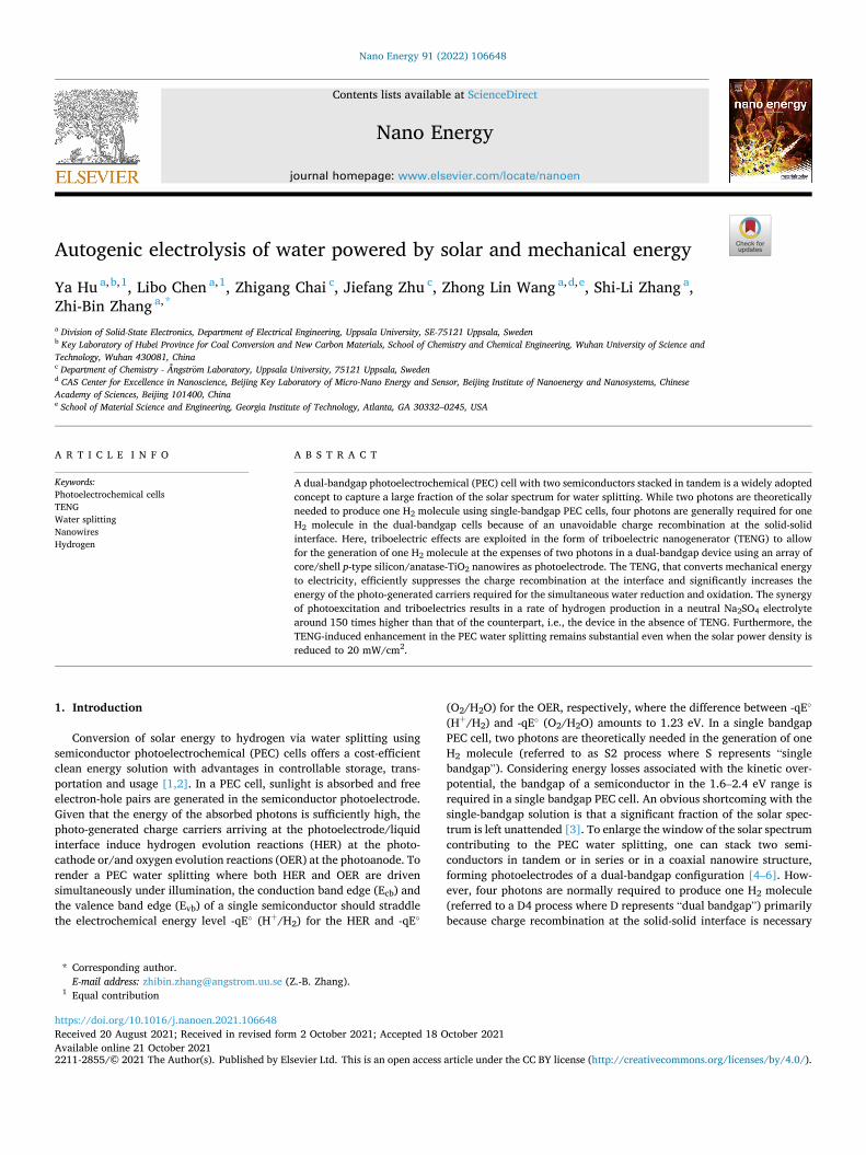
The microstructure of the p-SiNW/anatase-TiO2 core/shell nano-wires is shown in Fig. 2a and b for top-view and cross-sectional images from scanning electron microscopy (SEM), respectively. The p-SiNW arrays were prepared by metal-catalyzed electroless etching (MCEE) and the TiO2 layer (~20 nm in thickness) was grown by means of atomic layer deposition (ALD) (see Methods). The nanowires distribute fairly evenly with a diameter of ~50 nm and a length of ~2 µm. From the transmission electron microscopy (TEM) image in Fig. 2c, the SiNW is seen to be fully covered by the ALD-TiO2, with D = 0.35 nm indicating the lattice spacing of the (101) lattice planes of anatase TiO2. The conformal deposition of TiO2 on the SiNWs was confirmed by the high angle annular dark-field (HAADF) image under the scanning TEM (STEM) mode and the energy dispersive X-ray spectroscopy (EDS) im-ages of a Si/TiO2 nanowire (Fig. 2d).
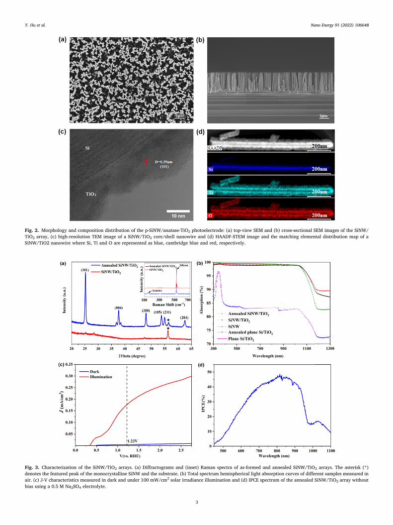
The crystalline anatase TiO2 protective layer can effectively prevent the SiNWs from being eroded in the electrolyte, which improves the stability of the nanowire electrode. In addition, defects and dislocations present in the anatase TiO2 lattice favor production of oxygen vacancies for electron capture enhancing therefore the photoelectrochemical ac-tivity of the photoelectrode [12–14]. The anatase phase of TiO2 was achieved by annealing the as-deposited ALD TiO2 coating on the SiNWs. As shown in Fig. 3a, the X-ray diffractogram of the as-formed SiNW/-TiO2 array only exhibits one diffraction peak marked by the asterisk indexed to Si(311) from the monocrystalline SiNWs and the Si substrate.
Fig. 1. Schematic illustration of (a) the hybrid PEC cell consisting of a SiNW/TiO2 (core/shell) photoelectrode and a Pt counter electrode, in between a TENG is connected, and the energy diagrams of the hybrid PEC cells under light illumination (b) without the TENG, (c) with the TENG providing a positive bias to the SiNW/ TiO2 where the D4 process occurs, and (d) with the TENG (T) providing a negative bias to the SiNW/TiO2 where the D2 process occurs, respectively.
Y. Hu et al.
Nano Energy 91 (2022) 106648
3
Fig. 2. Morphology and composition distribution of the p-SiNW/anatase-TiO2 photoelectrode: (a) top-view SEM and (b) cross-sectional SEM images of the SiNW/ TiO2 array, (c) high-resolution TEM image of a SiNW/TiO2 core/shell nanowire and (d) HAADF-STEM image and the matching elemental distribution map of a SiNW/TiO2 nanowire where Si, Ti and O are represented as blue, cambridge blue and red, respectively.
Fig. 3. Characterization of the SiNW/TiO2 arrays. (a) Diffractograms and (inset) Raman spectra of as-formed and annealed SiNW/TiO2 arrays. The asterisk (*) denotes the featured peak of the monocrystalline SiNW and the substrate. (b) Total spectrum hemispherical light absorption curves of different samples measured in air. (c) J-V characteristics measured in dark and under 100 mW/cm2 solar irradiance illumination and (d) IPCE spectrum of the annealed SiNW/TiO2 array without bias using a 0.5 M Na2SO4 electrolyte.
Y. Hu et al.

Nano Energy 91 (2022) 106648
4
After annealing, the TiO2 layer became crystallized and the character-istic diffraction peaks match well with the anatase phase of TiO2 (the power diffraction file 21–1272). No other phase could be found within the resolution limit of XRD. The diffraction data are consistent with the Raman results in the inset of Fig. 3a where the annealed SiNW/TiO2 array displays a peak at 144 cm− 1 (indicated by the arrow) that is characteristic of the anatase TiO2 [15]. The sharp feature of the Raman peak suggests the lack of amorphous TiO2. The anatase phase of the TiO2 coating leads to a significant enhancement in the absorption property of the annealed SiNW/TiO2 particularly in the NIR region (> 1000 nm) as compared to the as-formed SiNW/TiO2 (Fig. 3b). Below 1000 nm, the absorption approaches 99%. As a comparison, the absorption by blanket Si/TiO2 thin films prepared following the same procedure as that for
their nanowire counterparts is substantially reduced. The TiO2 absorp-tion edge appears only in the vicinity of ~350 nm. The excellent light absorption over the broad solar spectrum that the SiNW/anatase TiO2 array displays can boost the solar-to-fuel conversion efficiency.
The dual-bandgap heterostructure allowed the p-SiNW/n-anatase TiO2 array to harvest a large fraction of the solar spectral energy as clearly evidenced in Fig. 3(c) and (d) where the photoelectrochemical properties of the photoelectrode are displayed. Characterized in a 0.5 M Na2SO4 solution using the three-terminal configuration in the absence of TENG under 100 mW/cm2 solar irradiance illumination (AM 1.5G, see Method), the current density (J, unit: mA/cm2) of the annealed SiNW/ TiO2 array is found to continuously increase with the external potential (V). The current reaches a value of 0.18 mA/cm2 approximately at
Fig. 4. Electrical characterization of the hybrid PEC cell. (a) Equivalent circuit of the hybrid PEC cell with the RS-TENG, the SiNW/anatase TiO2 array as the photoelectrode and Pt as the counter electrode. Resistor (r = 470 Ω) was incorporated for current measurement. Performance evaluation of the hybrid PEC cell in a 0.5 M Na2SiO4 solution (b-f). (b) Time dependence of J when the RS-TENG was set to rotate at different rpm and output different negative bias voltage to the SiNW/ TiO2 array and the standard solar illumination (AM 1.5G, 100 mW/cm2) was alternately switched on (Jon) and off (Joff). Peak current at different rpm of the RS-TENG outputting. (c) Negative and (d) positive bias to the annealed SiNW/TiO2 array in dark or under the standard solar illumination (AM 1.5G, 100 mW/cm2). (e) Difference between Jon and Joff as a function of rpm of the RS-TENG with the TENG outputting negative (solid dots) and positive bias (solid squares) based, respectively, on data in (c) and (d). (f) Peak J as a function of peak voltage between the SiNW/TiO2 array and the Pt electrode when the RS-TENG output negative bias under standard solar illumination (solid circles) or in dark (solid squares). Inset: zoom-in of the curve under illumination.
Y. Hu et al.

Nano Energy 91 (2022) 106648
5
1.23 V vs. RHE (Fig. 3c). The turn-on voltage is ~0.34 V vs. RHE. The incident photon-to-current conversion efficiency (IPCE) of the annealed SiNW/TiO2 array measured in a two-electrode configuration shows a broad spectral light harvesting from UV to the NIR range (Fig. 3d). In the wavelength range used, a peak IPCE of ~45% is reached around 800 nm without bias. Since the anatase TiO2 can only absorb the light of wavelength below 390 nm, the IPCE spectrum shows that the photo- generated current is primarily attributed to the light absorption by the p-SiNWs.
In order to investigate the role of the RS-TENG in the PEC water splitting, a hybrid PEC cell was constructed using the annealed p-SiNW/ n-TiO2 array as the photoelectrode and a Pt wire as the counter elec-trode. As the equivalent circuit illustrated in Fig. 4a displays, the TENG output in the form of alternating current (AC) was transformed and rectified, providing a direct current (DC) to the electrodes. Fig. 4b shows the change of J in the hybrid PEC cell when the light source mimicking standard solar illumination (AM 1.5G, 100 mW/cm2) was switched on and off periodically at different TENG revolution speed, RSTENG. In this case, the outputted bias to the SiNW/TiO2 array was negative. Both J of light-off, Joff, and light-on, Jon, in the presence of the TENG operation increased with RSTENG of the RS-TENG, as Fig. 4b and c display. At 270 revolutions per minute (rpm), the peak current density was only ~0.02 mA/cm2 in dark. It increased by ~13.5 times to ~0.27 mA/cm2
under the standard solar illumination. It is shown in Fig. 4c that Jon increases much more substantially than Joff with RSTENG. At RSTENG of 1125 rpm, the peak Jon was ~3.36 mA/cm2, ~18.7 times higher than the counterpart Jon without the TENG contribution. On the other hand, when the bias from the TENG to the SiNW/TiO2 array was switched to positive, the peak Jon quickly increased when RSTENG was raised from 270 to 630 rpm. The peak Jon became saturated at ~2.38 mA/cm2 when RSTENG was further increased beyond 630 rpm (Fig. 4d).
To further shed light on the synergic effect of photo-excitation and TENG in water splitting, the increment in peak J caused by the 100 mW/ cm2 solar irradiance illumination and with the TENG operated at different rpm is shown in Fig. 4e. With the negative bias of the TENG output, the increment in peak J already reached ~0.25 mA/cm2 at 270 rpm. It increased continuously with the revolution speed and reached ~2.01 mA/cm2 at 1125 rpm. As a comparison, the increment in peak J was ~0.01 mA/cm2 at 270 rpm and slowly increased to and saturated at ~0.51 mA/cm2 beyond 770 rpm under the positive bias. This remarkable difference under the standard solar illumination can be understood by referring to the mechanism illustrated in Fig. 1. In the case of negative bias, the p-SiNW/n-TiO2 junction is reverse-biased and the photo-generated carrier recombination at the SiNW/TiO2 interface is efficiently suppressed. The hybrid PEC cell is thus set to work in the D2 mode and the separation and transportation of the photo-generated carriers are largely enhanced (Fig. 1d). An increase in negative bias accelerates the band bending in the cell, leading to a continuous rise in the increment of J under illumination. In the case of positive bias, the p- SiNW/n-TiO2 junction is forward biased (Fig. 1c). As the PEC reaction is governed by the D4 mechanism, the application of a positive bias simply increases the energy at the photocathode (i.e., Pt) to facilitate the water reduction and also bends the energy bands in favor of facilitating the charge transport in the p-SiNW and the TiO2 layer. As a result, the increment of J caused by illumination can also increase with the positive bias but not to the same extent as that under negative bias.
In order to further uncover the mechanism behind the significant enhancement of Jon under negative bias, the peak voltage between the SiNW/TiO2 array and the Pt electrode at different rpm was measured. Re-plotting the data in Fig. 4c but by replacing the revolution speed with the corresponding peak voltage as the x-axis, several observations can be made in Fig. 4f. First, the same range of revolution speeds can give rise to distinct ranges of peak voltage, i.e., 7.51–24.61 V in dark and 3.17–4.29 V under illumination. The change of peak voltage is mainly caused by the change in resistance of the region due to photo-generated charge carriers. Therefore, the peak voltage measured in dark is most
likely mainly the potential drop over the SiNW/TiO2 interface. Second, the peak J slowly increases in dark with the negative bias supplied by the TENG up to 20 V. This increase becomes accelerated when the peak voltage is above 20 V around which breakdown of the p-SiNW/n-TiO2 heterojunction occurs. Under illumination, the peak J steadily increases with the peak voltage from ~3.1 to ~3.8 V as shown in the inset of Fig. 4f. Further increase of the peak voltage leads to a steep rise in the peak J, which is indicative of the D2 process.
To characterize the hybrid PEC cell for water splitting, the H2 pro-duction as a function of reaction time under the standard solar irradi-ance illumination and with the TENG outputting negative bias was measured by using gas chromatography (Fig. 5a). A syringe was used to collect a small amount of the produced gas from the vial every 6 min during the water splitting process. Analysis of the produced gas showed that the water splitting speed was constant over time in the first 30 min as the volume of H2 linearly increased with time. Starting from 30 min, the water splitting began to accelerate due to the fact that H2 gas bubbles on the electrode grew in size and began to detach from the electrode. The amount of the produced H2 was 0.15 mL/cm2 measured at 36 min. Because numerous tiny bubbles still stayed on the electrode surface, a subsequent mechanical shake of the vial increased the amount from 0.15 to 0.38 mL/cm2. Therefore, the rate of H2 production in the neutral Na2SO4 electrolyte was ~10 μL/(cm2∙min), under the standard solar illumination and the TENG operation. As a comparison, the H2 pro-duction driven by the standard solar illumination in the absence of the TENG operation was much slower, as shown in the inset of Fig. 5a. To obtain a measurable amount of H2, the time interval for gas collection was set to 25 min. At 300 min, the amount of the H2 collected after shake was only 0.02 mL/cm2, equivalent to 6.7 × 10− 2 μL/(cm2⋅min). This rate is ~150 times lower than that with the TENG in operation. It has been previously reported that the use of the RS-TENG increased the speed of hydrogen production by 10 times on a PEC using a single- semiconductor (Fe2O3) photoelectrode [16]. The much more signifi-cant enhancement of the H2 evolution that our PEC cell has achieved implicates the important role of a p-n junction working in the enhanced D2 process by TENG. In order to characterize the overall solar-to-hydrogen (STH) efficiency of our hybrid PEC device in the neutral electrolyte in the absence of any sacrificial electron donors or acceptors, the STH efficiency is defined as the ratio of the chemical energy of the produced hydrogen to the solar energy input. Thus, the standard definition equation for the STH efficiency under the standard solar illumination can be expressed as:
STH = [(mmol H2/s) × (237000J/mol)
Ptotal(mW/cm2) × Area(cm2)]AM1.5G (1)
In the above equation the chemical energy of the produced hydrogen can be calculated from the rate of hydrogen production and the change in the Gibbs free energy per mole of H2 (ΔG0 = 237 kJ/mol at 25). In the denominator of eq.1, the input energy only includes the solar energy because the free charge carriers were generated by absorbing the pho-tons while the TENG provided additional energy to the photo-generated charge carriers by biasing. The denominator is the incident illumination power density (Ptotal, in units of mW/cm2) multiplied by the illuminated electrode area (cm2). Referring to Fig. 5a, the rate of H2 production in the neutral Na2SO4 electrolyte was ~10 μL/(cm2∙min), under the standard solar illumination and the TENG operation. The STH efficiency is 1.76% according to eq.1.
The synergic effect of photoexcitation and TENG in the H2 produc-tion prevailed with the hybrid PEC cell even when the solar illumination was reduced to 20 mW/cm2, as shown in Fig. 5b. The H2 production at each given solar irradiance intensity was obtained by water splitting for 25 min with the TENG outputting the negative bias at 270 rpm. Below 20 mW/cm2, the H2 production significantly drops. We found that the irradiance intensity of 20 mW/cm2 is equivalent to that in a normal indoor environment. The substantial enhancement in water splitting even under weak illumination and low speed of the RS-TENG shows that
Y. Hu et al.

Nano Energy 91 (2022) 106648
6
the hybrid PEC cell offers unique potential for practical applications because the solar irradiance not only changes periodically over time but also depends on the weather conditions.
It is worth emphasizing that the neutral Na2SO4 solution without adding any sacrificial agent was selected as the electrolyte in this work. The current commercial electrolytic cells use extremely acidic or alka-line electrolyte, which poses a great threat to the stability of semi-conductor electrode and the environment. For this reason, water splitting in near-neutral pH electrolytes or seawater has been pursued [17,18]. However, the neural and near-neutral electrolyte solutions have rather low concentration of proton/hydroxide ions. Reactants will be rapidly depleted during the proton-coupled electron transfer re-actions. Furthermore, due to the limitation of mass transfer, the re-supply of proton/hydroxide ions in the adjacent electrolyte area cannot be maintained, resulting in a concentration overpotential in addition to the kinetic overpotential of the electrocatalyst. As a conse-quence, hydrogen production in the neutral and near-neutral electro-lytes is rather slow [19]. It is a common way to increase proton donors and receptors to improve the limited ionic conductivity by adding sacrificial agents. This approach, however, suffers, from scalability in the PEC area, i.e., it is valid with small-area (<1 cm2) PEC devices, [19–21], unsustainability in the addition of the sacrificial regents, and the environment issue caused by the chemical agents. The rate of H2 production in the neutral Na2SO4 electrolyte, ~10 μL/(cm2∙min), has shown that our hybrid PEC cell is profound. A large room in the engi-neering of our PEC cell remains for increasing the PEC performances.
3. Conclusion
A self-powered hybrid PEC cell that comprises a dual-bandgap pho-toelectrode of p-SiNW/anatase TiO2 (core/shell) nanowire array and a RS-TENG for a high-speed autogenic water splitting is demonstrated. Integrating TENG in the hybrid PEC cell provides a self-powered means to suppress the carrier recombination in the SiNW/TiO2 photoelectrode, thereby allowing for the generation of one H2 at the expense of two photons, i.e., the D2 process, and to increase the energy of the charge carriers for simultaneous water reduction and oxidation. Using the neutral 0.5 M Na2SO4 electrolyte as the media, the hybrid PEC cell produces H2 at the rate of ~10 μL/(cm2∙min) that is 150 times higher than that of the PEC cell in the absence of the TENG. The enhancement in the hydrogen production remains substantial even when the solar irradiance intensity is reduced to ~20 mW/cm2 and the revolution speed of the RS-TENG is only 270 rpm. Thus, the hybrid PEC cell has high potential in real-life applications.
4. Experimental section
4.1. Fabrication of SiNW/TiO2 array photoelectrode
Vertically-aligned silicon nanowire arrays were synthesized on 1–10 Ω.cm p-Si (100) substrate wafer by means of metal-catalyzed electroless etching (MCEE) method. Briefly, single-crystalline silicon wafer was sliced to pieces of 10 cm by 10 cm in size. The pieces were first cleaned using standard RCA clean process. (Included in the first step was cleaning in a solution of 5 parts of deionized water, 1 part of ammonia water (29 wt%), 1 part of aqueous H2O2 (30 wt%), at 75 C for 10 min. The second step was cleaning in a different solution with 6 parts of deionized water, 1 part of aqueous HCl (37 wt%), 1 part of aqueous H2O2 (30 wt%), at 75 C for 10 min. The third step was a brief immer-sion in a diluted aqueous HF solution at 25 C for about 15 s. The fourth step was rinsing with deionized water and blown-drying by nitrogen on a rotating platform). Then, the cleaned silicon pieces were immersed into a HF-AgNO3 solution of 10 parts of deionized water, 1 part of AgNO3 (0.25 mol/L), and 2 part of aqueous HF (48 wt%) for 30 min. After this etching process, the surface gray silver dendrite film was carefully removed with tweezers to expose arrays of large-area verti-cally-aligned silicon nanowires. To completely remove the residual sil-ver particles, the as-prepared silicon wafer pieces were immersed in a concentrated nitric acid bath for 30 min, and then dipped into a diluted hydrofluoric acid (DHF) solution to remove the oxide layer on silicon nanowires. Finally, the prepared wafer pieces with nanowire arrays were rinsed with deionized water and dried. Subsequently, the wafer pieces were transferred into an atomic layer deposition system (ALD, Picosun R200) for TiO2 growth. The deposition chamber was evacuated to a base pressure of 0.3 kPa. Titanium tetrachloride and water served as the precursors for TiO2 growth and were pulsed alternately into the deposition chamber (heated to 200 C) with a 0.5 L min− 1 flow of N2 as carrier gas. Afterwards, a three-hour annealing at 450 C in nitrogen was applied to all SiNW/TiO2 samples to increase the crystallinity of the TiO2 film.
4.2. Structural characterization
The surface morphology was characterized on a high-resolution field emission-scanning electron microscope (Zeiss 1550 SEM/EDS) and transmission electron microscope (FEI Tecnai F30). The TEM specimen was prepared by scraping SiNWs/TiO2 nanowires into ethanol and then fully dispersed. The dispersion was drop-casted onto copper grids with a carbon coating. Energy-dispersive X-ray spectrometry (Oxford Inca) and selected area electron diffraction (SAED) were performed on a FEI Titan
Fig. 5. (a) Hydrogen production in the 0.5 M Na2SO4 electrolyte as a function of reaction time under the standard solar illumination and negative biasing by the TENG at the rotation speed of 1125 rpm and (inset) under the standard solar irradiance illumination only. Here “Shake” means that, at the end of the time, the data points in color were obtained after the cell was manually shaked before the measurement. (b) The H2 production as a function of solar irradiance with the negative bias of TENG at 270 rpm where the duration of H2 evolution is 25 min at each solar irradiance intensity.
Y. Hu et al.

Nano Energy 91 (2022) 106648
7
Themis in conjunction with using the TEM to determine material com-positions. All TEM and EDS data were obtained at an accelerating voltage of 200 keV. The crystal structure of the as-prepared samples was determined by means of X-ray diffraction with Cu Kα radiation (Bruker D8, Germany). X-ray photoelectron spectroscopy (XPS) was performed on a PHI Quantera II scanning XPS microprobe (Physical Electronics, Japan). The XPS C1s peak was calibrated to 284.8 eV and peak fitting was performed using a Gaussian-Lorentzian function after a Shirley background subtraction using CasaXPS software. Raman spectroscopy was carried out on a Renishaw Raman spectroscope with a 785 nm laser (20X objectives, 0.05 intensity).
4.3. Photoelectrochemical property characterization
Photoelectrochemical measurements were performed on an electro-chemical workstation (CH Instruments CHI660D) in a three-electrode configuration with the silicon substrate as the working electrode, the Pt wire as the counter electrode, and Ag/AgCl as the reference electrode. The measurements were done in a custom-made photoelectrochemical cell with an O-ring Quartz window. The rear side of the substrate was rubbed with liquid metal Ga/In eutectic mixture to form Ohmic contact. It was then attached to the photoelectrochemical cell. An aqueous electrolyte solution of 0.5 M Na2SO4 was used for both photo-electrochemical measurements and H2 evolution measurements. In a typical J–V measurement, the voltage was swept from 1.5 to − 1.5 V at a rate of 10 mV s− 1 under the illumination of an AM 1.5G solar simulator (100 mW/cm2, Newport Oriel LCS-100). For the TENG-induced enhancement measurements, the two-electrode configuration was employed with the substrate as the working electrode and the Pt wire as the counter electrode submerged in an aqueous electrolyte solution of 0.5 M Na2SO4.
4.4. H2 evolution measurement
To measure the amount of H2 produced, a homemade setup was built. The wafer piece was connected to an external wire from the rear side and sealed by epoxy resin. It worked as the photocathode. To complete the loop, a Pt wire was used as the counter electrode. Both electrodes were immersed into the 0.5 M Na2SO4 solution in a glass tube sealed with a rubber stopper. Both ends of the electrodes were connected to the TENG device from outside to form a complete circuit. The light source was provided by the same solar simulator as above (AM 1.5 G, Newport Oriel LCS-100) and the received solar irradiance was adjusted by the distance between the test device and the solar simulator. Each distance was calibrated with a power meter (Thorlabs PM160T). Before the measurement, the electrolyte was purged using Ar for 20 min in order to remove the dissolved gases from the electrolyte and fully fill up the emptied space of the glass test tube. Gas sample (50 μL) in the headspace of the tube was collected by a syringe and then analyzed by means of the gas chromatography (GC, PerkinElmer Autosystem XL) with a CarbonPLOT P7 column, using Ar as carrier gas. The H2 in the tube was detected by a thermal conductivity detector (TCD).
CRediT authorship contribution statement
Y.H. and L.C. jointly proposed the concept, fabricated and measured the samples, analysed data, prepared figures and references drafting and wrote part of the initial draft. Z.G.C. and J. Z. joined critical discussion and assisted in measurements; Z.L.W. provided crucial suggestions and provided critical feedback on the draft; S.L.Z. provided critical feedback on drafting; Z.B.Z. provided supervision, critical feedback on discus-sions, result interpretation and drafting.
Declaration of Competing Interest
The authors declare that they have no known competing financial
interests or personal relationships that could have appeared to influence the work reported in this paper.
Data availability statement
The data that support the findings of this study are openly available in [repository name e.g “figshare”] at http://doi.org/[doi], reference number [reference number].
Acknowledgement
Y. Hu and Z.-B. Zhang would like to thank Dr. Wei-Chao Chen and Prof. Charlotte Plazer Bjorkman for the support of IPCE measurements and Prof. Tomas Edvinsson for the support of absorption measurements. L. Chen would like to thank Dr. Yu Bai and Dr. Kai Han for the support of RS-TENG fabrication. This work was supported by the Swedish Research Council (Grant No. 2019–05484), Swedish Energy Agency (Grant No. 46641–1), Stiftelsen Olle Engkvist, Sweden (SOEB-2015/167) and the National Natural Science Foundation of China (Grant No. 61904130).
References
[1] O. Khaselev, J.A. Turner, A monolithic photovoltaic-photoelectrochemical device for hydrogen production via water splitting, Science 280 (1998) 425–427, https:// doi.org/10.1126/science.280.5362.425.
[2] S.Y. Reece, J.A. Hamel, K. Sung, T.D. Jarvi, A.J. Esswein, J.J. Pijpers, D.G. Nocera, Wireless solar water splitting using silicon-based semiconductors and earth- abundant catalysts, Science 334 (2011) 645–648.
[3] M.G. Walter, E.L. Warren, J.R. McKone, S.W. Boettcher, Q. Mi, E.A. Santori, N. S. Lewis, Solar water splitting cells, Chem. Rev. 110 (2010) 6446–6473.
[4] J.W. Jang, C. Du, Y. Ye, Y. Lin, X. Yao, J. Thorne, E. Liu, G. McMahon, J. Zhu, A. Javey, J. Guo, D. Wang, Enabling unassisted solar water splitting by iron oxide and silicon, Nat. Commun. 6 (2015) 7447, https://doi.org/10.1038/ncomms8447.
[5] M.T. Mayer, C. Du, D. Wang, Hematite/Si nanowire dual-absorber system for photoelectrochemical water splitting at low applied potentials, J. Am. Chem. Soc. 134 (2012) 12406–12409.
[6] X. Wang, K.-Q. Peng, Y. Hu, F.-Q. Zhang, B. Hu, L. Li, M. Wang, X.-M. Meng, S.- T. Lee, Silicon/hematite core/shell nanowire array decorated with gold nanoparticles for unbiased solar water oxidation, Nano Lett. 14 (2014) 18–23.
[7] Z.L. Wang, L. Lin, J. Chen, S. Niu, Y. Zi, Triboelectric Nanogenerators, Springer, 2016.
[8] Z.L. Wang, From contact-electrification to triboelectric nanogenerators, Rep. Prog. Phys. 84 (2021), 096502.
[9] H. Qin, G. Gu, W. Shang, H. Luo, W. Zhang, P. Cui, B. Zhang, J. Guo, G. Cheng, Z. Du, A universal and passive power management circuit with high efficiency for pulsed triboelectric nanogenerator, Nano Energy 68 (2020), 104372.
[10] W. Shang, G. Gu, W. Zhang, H. Luo, T. Wang, B. Zhang, J. Guo, P. Cui, F. Yang, G. Cheng, Rotational pulsed triboelectric nanogenerators integrated with synchronously triggered mechanical switches for high efficiency self-powered systems, Nano Energy 82 (2021), 105725.
[11] L. Chen, C. Wen, S.-L. Zhang, Z.L. Wang, Z.-B. Zhang, Artificial tactile peripheral nervous system supported by self-powered transducers, Nano Energy 82 (2021), 105680.
[12] Q. Guo, C. Zhou, Z. Ma, X. Yang, Fundamentals of TiO2 photocatalysis: concepts, mechanisms, and challenges, Adv. Mater. 31 (2019), e1901997, https://doi.org/ 10.1002/adma.201901997.
[13] R. Katal, S. Masudy-Panah, M. Tanhaei, M.H.D.A. Farahani, H. Jiangyong, A review on the synthesis of the various types of anatase TiO2 facets and their applications for photocatalysis, Chem. Eng. J. 384 (2020), 123384.
[14] J. Zheng, Y. Lyu, R. Wang, C. Xie, H. Zhou, S.P. Jiang, S. Wang, Crystalline TiO2 protective layer with graded oxygen defects for efficient and stable silicon-based photocathode, Nat. Commun. 9 (2018) 3572, https://doi.org/10.1038/s41467- 018-05580-z.
[15] S. Chen, Y. Wang, J. Li, Z. Hu, H. Zhao, W. Xie, Z. Wei, Synthesis of black TiO2 with efficient visible-light photocatalytic activity by ultraviolet light irradiation and low temperature annealing, Mater. Res. Bull. 98 (2018) 280–287.
[16] A. Wei, X. Xie, Z. Wen, H. Zheng, H. Lan, H. Shao, X. Sun, J. Zhong, S.T. Lee, Triboelectric nanogenerator driven self-powered photoelectrochemical water splitting based on hematite photoanodes, ACS Nano 12 (2018) 8625–8632, https:// doi.org/10.1021/acsnano.8b04363.
[17] X. Zhou, R. Liu, K. Sun, D. Friedrich, M.T. McDowell, F. Yang, S.T. Omelchenko, F. H. Saadi, A.C. Nielander, S. Yalamanchili, Interface engineering of the photoelectrochemical performance of Ni-oxide-coated n-Si photoanodes by atomic- layer deposition of ultrathin films of cobalt oxide, Energy Environ. Sci. 8 (2015) 2644–2649.
[18] C.-T. Lee, L.-I. Hung, Y.-C. Shih, J.C.-S. Wu, S.-L. Wang, C.-W. Huang, V.- H. Nguyen, Solar hydrogen production from seawater splitting using mixed- valence titanium phosphite photocatalyst, J. Environ. Chem. Eng. 9 (2021), 104826.
Y. Hu et al.

Nano Energy 91 (2022) 106648
8
[19] K. Obata, R. van de Krol, M. Schwarze, R. Schomacker, F.F. Abdi, In situ observation of pH change during water splitting in neutral pH conditions: impact of natural convection driven by buoyancy effects, Energy Environ. Sci. 13 (2020) 5104–5116.
[20] L. Pan, J.H. Kim, M.T. Mayer, M.-K. Son, A. Ummadisingu, J.S. Lee, A. Hagfeldt, J. Luo, M. Gratzel, Boosting the performance of Cu 2 O photocathodes for unassisted solar water splitting devices, Nature Catal. 1 (2018) 412–420.
[21] I.Y. Ahmet, Y. Ma, J.-W. Jang, T. Henschel, B. Stannowski, T. Lopes, A. Vilanova, A. Mendes, F.F. Abdi, R. van de Krol, Demonstration of a 50 cm 2 BiVO 4 tandem photoelectrochemical-photovoltaic water splitting device, Sustain. Energy Fuels 3 (2019) 2366–2379.
Ya Hu is currently an associate professor at the school of chemistry and chemical engineering, Wuhan University of Science and Technology(WUST), China. She received her Ph.D. degree in Condensed Matter Physics from Beijing Normal University in 2015. She engaged in the research work in Pro-fessor Stuart Parkin’s group in Max Planck Institute of Micro-structure Physics, Germany served as postdoctor research fellow and then joined in WUST. From 2018 she works as a visiting researcher at division of solid-state electronics, Uppsala University, Sweden. Her research interests include electrochemical etching technology and application of ultra-fine nano silicon materials.
Libo Chen received his B.S. degree in Physics from Zhengzhou University in 2013, and his Ph.D. degree in Condensed Matter Physics from University of Chinese Academy of Sciences in 2018 under the supervision of Prof. Zhong Lin Wang. He is now a postdoctoral fellow at Uppsala University. His research in-terests include triboelectric nanogenerator, electronic skin and artificial nervous system.
Zhong Lin Wang is the Hightower Chair in Materials Science and Engineering and Regents’ Professor at Georgia Tech, and Founding Director of the Beijing Institute of Nanoenergy and Nanosystems. Dr. Wang pioneered the field of nanogenerators and self-powered sensors, and coined piezotronics and piezo- phototronics for the third-generation semiconductors.
Shi-Li Zhang is chair professor of the discipline “Solid State Electronics” and head of the Division of Solid-State Electronics at Uppsala University, Sweden. The Division is currently organised in seven research groups focusing on research areas (1) Electronics for life sciences; (2) Electronics for biomedical technology; (3) Electronics for next-generation computing; (4) and Electronics for self-powered and energy-efficient systems. As an experimentalist, Zhang is specialised in silicon technol-ogy and microelectronics/nanoelectronics spanning from physics of semiconductor devices, materials science and various process techniques/modules for device design, fabri-cation and characterisation. During the latest two decades, he has also been exploring nanobiosensors and flexible electronics
based on silicon nanofabrication technology.
Zhi-Bin Zhang was appointed as docent in electronics at Uppsala University in 2013. He completed his bachelor and master in physics at Lanzhou University, China, in 1993 and 1997, respectively. In 2001, He obtained his PhD degree in applied physics at Shanghai Institute of Applied Physics, Chi-nese Academy of Sciences. He has worked in School of Infor-mation and Communication Technology at Royal Institute of Technology, Sweden, from 2002 to 2010. Since 2011, he joined in Department of Engineering Sciences at Uppsala University. His research scope has been primarily on electronic materials for printed and flexible electronic devices, electric sensors, thin film transistors, thermoelectric devices, electronic skin and neuromorphic circuits.
Y. Hu et al.