automatic generation of interrupt-aware hardware ... · machine code into a hardware design...
TRANSCRIPT

Automatic Generation of Interrupt-Aware Hardware
Accelerators with the M2V Compiler
Abilash Sekar, Alessandro Forin
Microsoft Research
August 2008
Technical Report
MSR-TR-2008-110
Microsoft Research
Microsoft Corporation
One Microsoft Way
Redmond, WA 98052

- 2 -

- 3 -
Automatic Generation of Interrupt-Aware Hardware
Accelerators with the M2V Compiler
Abilash Sekar, Alessandro Forin
Microsoft Research
Abstract
The MIPS-to-Verilog (M2V) compiler and the Basic
Block Tools (BBTools) can automatically generate a
hardware accelerator for selected blocks of machine code
in an application. The compiler translates blocks of MIPS
machine code into a hardware design captured in Verilog
(an "Extension"). The BBTools patch the application
binary by inserting the extension instruction that triggers
the accelerator. The original code is preserved, so that
execution can fall back to software when necessary.
This work extends the M2V compiler with support for
memory load and store instructions, and for interrupts.
We use a transactional model to handle interrupts and/or
traps due to TLB misses in the Extension. We implemented
and tested the interrupt support mechanism using a 64-bit
division basic block, with added instructions for memory
loads off the stack pointer.
We also added the feature of allowing the BBTools to
automatically create the best encoding for an extension
instruction. The tool now evaluates which pair of roots in
the dependency graph leads to the shortest execution
cycle time for the Extension. With this addition, the
process of creating Extensions for the eMIPS processor
can now be fully automated and applied to practical
applications, where loads and stores inside the Extension
are of paramount importance.
1 Introduction
Extensible processors have a simple RISC pipeline
and the ability to augment the Instruction Set Architecture
(ISA) with custom instructions. The ISA can be
augmented statically, at tape-out, or it can be augmented
dynamically when applications are loaded. Extensible
processors differ from other accelerators in their tight
integration with the basic data path, which leads to
minimal latencies and therefore greater flexibility.
Examples of dynamically extensible processors include
eMIPS [6] and Stretch [13]. Tensilica’s Xtensa [14] is an
example of a statically extensible processor.
Extensible processors take advantage of the fact that a
small amount of code takes the majority of execution time
in a typical program. The code that executes most often is
a candidate for hardware acceleration. The code is
identified by a special instruction that will initiate the
accelerator.
*.EXE
Compiled
Binary
Executable
BB Tools
GIANO
Simulator*.EXE
Patched Binary
*.BBW
Extension
Basic Block File
M2V
(MIPS to
Verilog
Compiler)
*.V
Synthesizable
Verilog
Figure 1: The eMIPS Tool Chain to automate the
generation of hardware accelerators.
Selection of the best code to accelerate is an active
area of research. The eMIPS tool-chain, shown in Figure
1, restricts the code selection problem to the set of basic
blocks in the application. Using the strict definition in [1],
the basic block is a directed acyclic graph (DAG). A
DAG is a set of machine instructions that do not contain
branches and are branched-to only for the very first
instruction. The best candidate blocks are currently
selected by executing the application using the Giano full-
system simulator [21], in concert with the data obtained
via static analysis of the application binary. The BBTools
select the basic blocks to accelerate and patch the binary
image with the special instructions for the accelerator.
The M2V compiler [16] automatically generates the
design for the hardware accelerator, which is then
synthesized using the Xilinx tools for the ML40x boards.
The accelerator can be statically loaded when eMIPS
is reset or it can be dynamically loaded when an
application is loaded using partial reconfiguration of the
FPGA. By dynamically loading and unloading
accelerators, the area of the programmable hardware can
be used more efficiently.
In previous versions of eMIPS, the accelerator blocks
could be specified and given to a hardware designer to
hand design the accelerator. While this can lead to an
efficient implementation, manual designs do not scale well

- 4 -
as dynamically extensible processors are more widely
used and the hardware becomes more complex. To
effectively utilize dynamically extensible processors,
different parts of an application can be accelerated using
different Extensions, which can be loaded at appropriate
times. The use of the tool chain along with M2V can
expand the use of hardware acceleration and completely
automate the process of generating hardware accelerators
for a variety of basic blocks in an application.
The work described herein addresses three limitations
in the tool chain that prevented the M2V tool chain from
being usable in but a few practical cases. The first
limitation was the lack of support for load and store
operations, and more generally for variable-cost
operations. M2V was previously only able to cope with
MIPS instructions that took zero or one cycle. We added
support for all the instructions that took a fixed number of
cycles, accounting for the cost in the generation of the
schedule. Then we added support for the instructions that
have variable costs, prime and foremost loads and stores.
We were able to find a way to preserve the overall
structure of the compiler, while dealing with the variable
costs. The dependency graph still leads to a state machine
that controls the overall execution. The transitions are now
defined not only by the clock, but also by the signals that
indicate completion of the variable-cost operations.
The second limitation concerns the inability of the
M2V compiler to generate logic for handling interrupts
within an Extension. External interrupts could only
happen before or after the extension instruction, never
inside it. This assumption is invalid in the presence of
TLB misses due to loads and stores. Furthermore, the
previous tool required that an Extension never encounter
errors, such as arithmetic overflows or unaligned
addresses. For a real-time system, it is important to
respond to interrupts in a timely and predictable manner.
Even in a general-purpose OS it is unacceptable to allow a
user process to ignore interrupts and lock the machine. To
address the interrupt limitation, we used the concept of
transactions in dealing with the write-backs to the register
file and the stores to memory. The overall execution of the
Extension is subdivided in sets that execute “atomically”.
Interruptions of any sort are accepted at the transaction
boundaries. On interruption, the write-back machine
cancels all write-backs from future transactions, completes
the write-backs for the current one, and then relinquishes
control back to the data-path in a limited amount of time.
The restart-address is set to the point in the original basic
block that corresponds to the current write-back state. It is
therefore mandatory that extension instructions are simply
inserted in the original image, and that they do not replace
the original basic block.
The third limitation addresses the task of
automatically choosing an instruction encoding for the
new extension instruction. We observed that the selection
of which registers or constants to encode in the instruction
can have an effect on the overall execution time. These
values are available early in the execution pipeline. It is
therefore important to select those that allow the most
work to proceed before stalling on a dependency. Our
algorithm uses two parameters in deciding which two
register numbers to encode – fan-out and depth of the root
register read nodes. It selects the pair of registers with the
maximum combined fan-out and depth.
The remainder of this document is structured as
follows. Section 2 discusses related work. Section 3 gives
an overview of the eMIPS hardware platform. Section 4
discusses the automatic encoding of the extension
instruction by the BBTools. Section 5 defines the support
for memory operations in the M2V compiler. Section 6
discusses the model and implementation for handling
interrupts in the Extension. Section 7 explains the M2V
generated hardware in more detail. Section 8 compares
the synthesis reports obtained for Extensions generated
with and without the transactional model enabled. Section
9 discusses the experimental results, and Section 10
concludes the report. Appendix I contains the BBW file
for the example basic block. Appendix II contains
synthesis reports for the Extension generated by the M2V
compiler. Appendix III contains the Verilog output from
M2V, with the transactional model enabled and interrupt
support. Appendix IV shows an automated visualization
of the dependency graphs from M2V.
2 Related Work
Work on extensible processors can be divided in
several ways. One avenue of exploration is to define the
underlying hardware. Chimaera [7] and GARP [8] are
two examples of extensible hardware from the late 1990’s.
Commercial FPGA manufacturers today all provide
examples of soft-cores, microprocessor designs that the
customer can modify and extend for their application [15,
3, 13]. M2V uses the eMIPS processor [6] as its
underlying hardware platform. eMIPS is the first design
that is secure for general purpose multi-user loads, and the
set of potential applications is therefore more open-ended
than those found in the typical embedded system alone.
A common approach to generate code for an
extensible processor is to modify an existing C compiler.
Tensilica [14] automatically regenerates a full GNU
compilation system given the RTL of the new instruction.
Ienne et al. [4] use the SUIF compiler. M2V accepts as
input binary machine code rather than source code. There
are trade-offs between accelerating from source code in a

- 5 -
high-level language or from binaries. One of the major
advantages when accelerating from binaries is that any
application can be accelerated, even applications where
the source code is controlled by an outside party and not
available to the system developer. A disadvantage is that
some of the information that has been discarded must be
reconstructed, and there are limits to this reversal process.
The FREEDOM compiler [17, 18] is similar to M2V;
the compiler accepts binary machine code as input and
maps it to an FPGA. The Extensions generated by the
M2V compiler are meant for a general-purpose
environment and therefore execute in coordination with
the main processor data path, whereas FREEDOM maps
the entire program to the bare FPGA. M2V generates
Extensions that are explicitly interrupt-aware, whereas
there is no mention of handling interrupts in the
FREEDOM compiler. Additionally, the Extensions
generated by the M2V compiler for the eMIPS have
secure access to the memory subsystem via the Memory
Management Unit (MMU), which is not a requirement for
the DSP-like programs handled by the FREEDOM
compiler. FREEDOM is a more mature product and can
handle a larger body of codes than what M2V currently
does.
Another avenue of research in extensible processors
is the identification of the Instruction Set Extensions (ISE)
that most benefit a given program, see for instance [5] for
a recent overview. Bonzini [5] advocates generating the
ISE from within the compiler, Tensilica [14] from
profiling data. M2V currently follows the application
profiling approach; it uses the BBTools and dynamic full-
system simulation with Giano to select the candidate basic
blocks. The current approach can extend to handling
chains of blocks e.g. in frequently executed loops that are
automatically recognized via full-system simulation [19].
A possible addition to our work is to use M2V in concert
with a high-level compiler. Once the ISE is identified
from within the compiler, the Extension’s definition could
be output in the form of a BBW file.
A related area is the generation of HDL code from C,
the so-called C-to-gates design flows [11, 12]. The
common target is the automated generation of HDL code
from sequential programs. The main difference with M2V
is that the input is binary code. Using binary code supports
all programming languages, included dynamically
generated (jitted) code. It is the only viable option in case
the high level source code is not available, e.g. for third-
party code and libraries. The drawback is that makes the
problem harder. The binary code has already been
optimized (register allocation, loop unrolling, etc) during
its compilation hence identifying parallelism is more
difficult. The BBTools framework tries to account for
some of these optimizations by using a canonical form of
the basic block, so that it can identify repeating basic
blocks in the binary.
3 eMIPS Hardware Overview
The extensible MIPS (eMIPS) processor [6] has been
developed at Microsoft Research as an example of a RISC
processor integrated with programmable logic. The
programmable logic has many uses, such as: extensible
on-line peripherals, zero overhead online verification of
software, hardware acceleration of general-purpose
applications, and in-process software debugging [2]. This
document is concerned with automatically generating
hardware accelerators within the context of the eMIPS
extensible processor.
The instruction set for the eMIPS processor is the
instruction set for the R4000 MIPS processor [10]. The
R4000 is an example of a classic RISC architecture. The
eMIPS pipeline follows the classic RISC pipeline [9]
consisting of five stages: instruction fetch (IF), instruction
decode (ID), execute (EX), memory access (MA), and
register write-back (WB).
The eMIPS processor departs from a standard RISC
processor by adding an interface to programmable logic.
The programmable logic is tightly integrated with the
RISC pipeline, it can synchronize with it and it can access
the same resources as the RISC pipeline. Figure 2 shows
a logical block diagram for the eMIPS processor. The
tight coupling of the pipeline and programmable logic
creates a very low latency interface between the
accelerator and the RISC pipeline.
Figure 3 illustrates the pipelining of instructions
through eMIPS. The decode logic in the extension logic
is always an observer of the main pipeline and is trying to
Ex.
(ALU) MA WB
Soft
Fabric
IF ID
Hard Fabric:
TISA
Inter Pipeline Traffic
CP0
(Exception
Handler)
Memory
(MMU, Cache) Registers
Peripheral Ext. 2
Execution
Blocks Ext. 1 Ext. 1
ID
Ext. 2
ID Extensions
Figure 2. eMIPS block diagram. The Soft Fabric can
be reconfigured at run time to extend the ISA.
kk
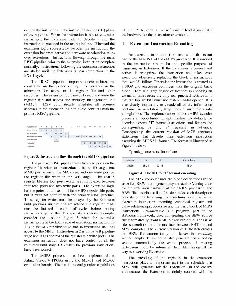
- 6 -
decode the instruction in the instruction decode (ID) phase
of the pipeline. When the instruction is not an extension
instruction, the Extension fails to decode it and the
instruction is executed in the main pipeline. If instead the
extension logic successfully decodes the instruction, the
extension becomes active and hardware acceleration takes
over execution. Instructions flowing through the main
RISC pipeline prior to the extension instruction complete
normally. Instructions following the extension instruction
are stalled until the Extension is near completion, in the
EXn-1 cycle.
The RISC pipeline imposes micro-architectural
constraints on the extension logic, for instance in the
arbitration for access to the register file and other
resources. The extension logic needs to read and write the
register file and access the memory management unit
(MMU). M2V automatically schedules all resource
accesses in the extension logic to avoid conflicts with the
primary RISC pipeline.
IF ID EX MA
EX1
WB
IF ID EX MA WB
IF ID EX2 MA WBEXn-1Exn-2 EXn...
IF ID EX MA WB
IF ID EX MA WB
Instruction m-2
Instruction m-1
Extension Instruction m
Instruction j
Instruction j+1
Cycle Number 0 1 2 3 4 5 n+2 n+3 n+4 n+5 n+6 n+7 n+8...
IFInstruction m+1
Figure 3: Instruction flow through the eMIPS pipeline.
The primary RISC pipeline uses two read ports on the
register file when an instruction is in the ID stage, one
MMU port when in the MA stage, and one write port on
the register file when in the WB stage. The eMIPS
register file has four ports which are multiplexed between
four read ports and two write ports. The extension logic
has the potential to use all of the eMIPS register file ports,
but it must not conflict with the primary RISC pipeline.
Thus, register writes must be delayed by the Extension
until previous instructions are retired and register reads
must be finished a couple of cycles before trailing
instructions get to the ID stage. As a specific example,
consider the case in Figure 3 when the extension
instruction is in the EX1 cycle of execution, instruction m-
1 is in the MA pipeline stage and so instruction m-1 has
access to the MMU. Instruction m-2 is in the WB pipeline
stage and it has control of the register file write ports. The
extension instruction does not have control of all the
resources until stage EX3 when the previous instructions
have been retired.
The eMIPS processor has been implemented on
Xilinx Virtex 4 FPGAs using the ML401 and ML402
evaluation boards. The partial reconfiguration capabilities
of this FPGA model allow software to load dynamically
the hardware for the instruction extensions.
4 Extension Instruction Encoding
An extension instruction is an instruction that is not
part of the base ISA of the eMIPS processor. It is inserted
in the instruction stream for the specific purpose of
triggering an Extension. If the Extension is present and
active, it recognizes the instruction and takes over
execution, effectively replacing the block of instructions
that (would) follow. Otherwise the instruction is treated as
a NOP and execution continues with the original basic
block. There is a large degree of freedom in encoding an
extension instruction; the only real practical restriction is
that the top six bits must not match a valid opcode. It is
also clearly impossible to encode all of the information
contained in an arbitrarily large block of instructions into
a single one. The implementation of the eMIPS decoder
presents an opportunity for optimization. By default, the
decoder expects "I” format instructions and fetches the
corresponding rs and rt registers in advance.
Consequently, the current revision of M2V generates
Extensions that decode their extension instruction
assuming the MIPS “I” format. The format is illustrated in
Figure 4 below.
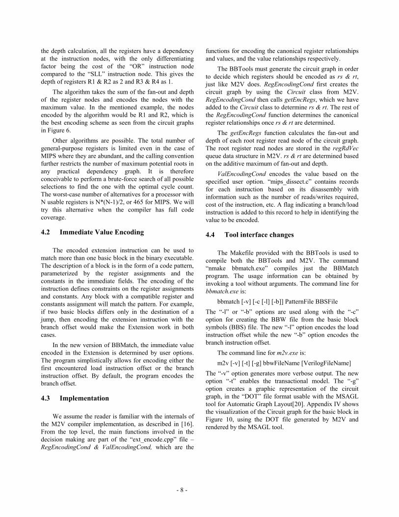
Opcode_name rt, rs, immediate
31:26 25:21 20:16 15:0
opcode rs rt immediate
Figure 4: The MIPS “I” format encoding.
The M2V compiler uses the block descriptions in the
so-called BBW file to generate synthesizable Verilog code
for the Extension hardware of the eMIPS processor. The
BBW file describes a list of basic blocks; each description
consists of the following main sections: machine name,
extension instruction encoding, canonical register and
value relationships, code size and the basic block of MIPS
instructions. BBMatch.exe is a program, part of the
BBTools framework, used for creating the BBW source
file automatically, from a MIPS executable file. The BBW
file is therefore the core interface between BBTools and
M2V compiler. The current version of BBMatch creates
the BBW file automatically, but leaves the encoding
section empty. If we could also generate the encoding
section automatically the whole process of creating
Extensions could be automated, from ELF image all the
way to a working Extension.
The encoding of the registers in the extension
instruction plays an important part in the schedule that
M2V will generate for the Extension. In the eMIPS
architecture, the Extension is tightly coupled with the

- 7 -
standard MIPS pipeline. This gives us the advantage of
having the two registers rs & rt, encoded in the extension
instruction, available directly from the decode stage of the
MIPS pipeline. This feature can be used to reduce the
execution time of the Extension by appropriately selecting
the registers to encode in the extension instruction. This is
illustrated by the simple example basic block shown
below in Figure 5. The cost of the “OR” and the “SLL”
instructions in the basic block are 1 and 0 cycles
respectively. We shall consider two cases to illustrate the
importance of encoding the correct registers.
[0] ext0 rx, ry, offset
[4] or r5, r1, r2
[8] sll r6, r3, r4
Figure 5: The choice of rx and ry in this basic block
affects the performance of the generated Extension.
The circuit graph generated by M2V is shown in
Figure 6 for two different encodings of the extension
instruction. In the graphs, the clock cycle when the
respective node completes is depicted next to the node.
RF
Read
R1
RF
Read
R2
RF
Read
R3
RF
Read
R4
SLLOR
RF
Write
R5
RF
Write
R6
cyc 1
cyc 4cyc 4
cyc 4
cyc 5 cyc 6
Case (i): Extension instruction encoded with R1, R2
Key:
State 3
State 2
State 1
State 4
RF
Read
R1
RF
Read
R4
SLLOR
RF
Write
R5
RF
Write
R6
RF
Read
R3
RF
Read
R2
cyc 4 cyc 4
cyc 4cyc 5
cyc 6cyc 7
Case (ii): Extension instruction encoded with R1, R3
Figure 6: Circuit graphs for the block in Figure 2,
using different encoding schemes.
The graphs show that though the number of states in
the Extension remains the same, the number of clock
cycles taken by the Extension to execute the set of
instructions differs based on the encoding of the registers.
Considering the first case, registers R1 and R2 are
encoded, thus making them available directly from the
decode phase of the pipeline in stage 2 of the extension
state machine. The “OR” instruction can be executed
immediately, and will complete in cycle 1 since the
Extension has all the registers available and no unmet
dependencies. However, the “SLL” instruction requires
both source registers to be read from the register file,
which takes 4 clock cycles. This causes the SLL
instruction to complete in cycle 4. A pipeline stage is
inserted by the extension state machine after execution of
the instructions at cycle 4. The two register write-backs
are performed after the pipeline stage, in cycle 5 (R5) and
cycle 6 (R6). Thus, the Extension requires 6 cycles to
complete execution with this encoding.
Considering the second case, registers R1 and R3 are
encoded. In this case, none of the instructions can be
executed directly as both have unmet dependencies and
require register reads from the register file. Assuming
there are at least two read ports in the register file, the OR
instruction completes after 5 cycles, 4 cycles for reading
register R2 and 1 cycle for execution. Similarly, the SLL
instruction completes execution in cycle 4. Again, a
pipeline stage is inserted after execution of the
instructions in cycle 5. The register write-backs are
performed in cycle 6 (R6) and cycle 7(R5). Thus the
Extension requires 7 cycles to complete execution with
this encoding.
In this minimal example, a two instruction basic block
shows a difference of 1 execution cycle depending on the
selected encoding. The encoding scheme will have a
greater impact on the execution time when there are long
latency paths in the basic block. Thus, it is of prime
importance to create an optimal encoding of the
Extension’s registers to reduce Extension latency.
4.1 Register Selection Algorithm
In the new version of “bbmatch.exe”, the encoding
algorithm uses two main parameters in selecting the rs &
rt registers – fan-out and depth of the root register read
nodes. Fan-out is the number of instructions dependent on
the root register read node. Depth is a count of the register
nodes and the cost of the instruction nodes till a
dependency is met in the graph.
Using the circuit graphs in Figure 6, all the register
read nodes, R1, R2, R3 and R4 have a fan-out of 1. For
- 8 -
the depth calculation, all the registers have a dependency
at the instruction nodes, with the only differentiating
factor being the cost of the “OR” instruction node
compared to the “SLL” instruction node. This gives the
depth of registers R1 & R2 as 2 and R3 & R4 as 1.
The algorithm takes the sum of the fan-out and depth
of the register nodes and encodes the nodes with the
maximum value. In the mentioned example, the nodes
encoded by the algorithm would be R1 and R2, which is
the best encoding scheme as seen from the circuit graphs
in Figure 6.
Other algorithms are possible. The total number of
general-purpose registers is limited even in the case of
MIPS where they are abundant, and the calling convention
further restricts the number of maximum potential roots in
any practical dependency graph. It is therefore
conceivable to perform a brute-force search of all possible
selections to find the one with the optimal cycle count.
The worst-case number of alternatives for a processor with
N usable registers is N*(N-1)/2, or 465 for MIPS. We will
try this alternative when the compiler has full code
coverage.
4.2 Immediate Value Encoding
The encoded extension instruction can be used to
match more than one basic block in the binary executable.
The description of a block is in the form of a code pattern,
parameterized by the register assignments and the
constants in the immediate fields. The encoding of the
instruction defines constraints on the register assignments
and constants. Any block with a compatible register and
constants assignment will match the pattern. For example,
if two basic blocks differs only in the destination of a
jump, then encoding the extension instruction with the
branch offset would make the Extension work in both
cases.
In the new version of BBMatch, the immediate value
encoded in the Extension is determined by user options.
The program simplistically allows for encoding either the
first encountered load instruction offset or the branch
instruction offset. By default, the program encodes the
branch offset.
4.3 Implementation
We assume the reader is familiar with the internals of
the M2V compiler implementation, as described in [16].
From the top level, the main functions involved in the
decision making are part of the “ext_encode.cpp” file –
RegEncodingCond & ValEncodingCond, which are the
functions for encoding the canonical register relationships
and values, and the value relationships respectively.
The BBTools must generate the circuit graph in order
to decide which registers should be encoded as rs & rt,
just like M2V does. RegEncodingCond first creates the
circuit graph by using the Circuit class from M2V.
RegEncodingCond then calls getEncRegs, which we have
added to the Circuit class to determine rs & rt. The rest of
the RegEncodingCond function determines the canonical
register relationships once rs & rt are determined.
The getEncRegs function calculates the fan-out and
depth of each root register read node of the circuit graph.
The root register read nodes are stored in the regRdVec
queue data structure in M2V. rs & rt are determined based
on the additive maximum of fan-out and depth.
ValEncodingCond encodes the value based on the
specified user option. “mips_dissect.c” contains records
for each instruction based on its disassembly with
information such as the number of reads/writes required,
cost of the instruction, etc. A flag indicating a branch/load
instruction is added to this record to help in identifying the
value to be encoded.
4.4 Tool interface changes
The Makefile provided with the BBTools is used to
compile both the BBTools and M2V. The command
“nmake bbmatch.exe” compiles just the BBMatch
program. The usage information can be obtained by
invoking a tool without arguments. The command line for
bbmatch.exe is:
bbmatch [-v] [-c [-l] [-b]] PatternFile BBSFile
The “-l” or “-b” options are used along with the “-c”
option for creating the BBW file from the basic block
symbols (BBS) file. The new “-l” option encodes the load
instruction offset while the new “-b” option encodes the
branch instruction offset.
The command line for m2v.exe is:
m2v [-v] [-t] [-g] bbwFileName [VerilogFileName]
The “-v” option generates more verbose output. The new
option “-t” enables the transactional model. The “-g”
option creates a graphic representation of the circuit
graph, in the “DOT” file format usable with the MSAGL
tool for Automatic Graph Layout[20]. Appendix IV shows
the visualization of the Circuit graph for the basic block in
Figure 10, using the DOT file generated by M2V and
rendered by the MSAGL tool.
- 9 -
5 Memory access support in M2V
This section describes our additions to the M2V
compiler to support memory accesses. It is well known in
the literature that the lack of load and store operations
leads to limited speedups from hardware acceleration. The
operations are not only important for performance, but in
our experience they are almost always present in the most-
frequently executed basic blocks of an application,
precisely the blocks that M2V wants to speed up.
M2V is a three-pass compiler which automatically
generates eMIPS Extensions from a BBW source file. The
first pass processes the BBW file and consists of three
major steps: map the encoding for the extension
instruction to the basic block, analyze the MIPS
instructions, and build a circuit graph. The second pass
schedules the operations that are represented in the graph.
The third pass emits the Verilog that will be synthesized
and placed in the eMIPS FPGA.
The eMIPS architecture allows for Extensions to
access memory through the MMU just like the main MIPS
processor data path. The MMU is part of the Trusted ISA
portion of the eMIPS processor; The MMU is the only
path to memory available to general, untrusted Extensions.
The Extension is tightly coupled with the main MIPS
pipeline. The Extension has access to the memory
interface only after a few cycles it received control. This
restriction is taken care of in the scheduling pass of the
M2V compiler. To ensure correct execution of the
memory instructions, the Extension must obey the
protocols shown below in Figure 7 and Figure 8. The
M2V compiler generates this logic using the scheduling of
memory instructions and the states of the extension state
machine. The protocols for the memory read and write
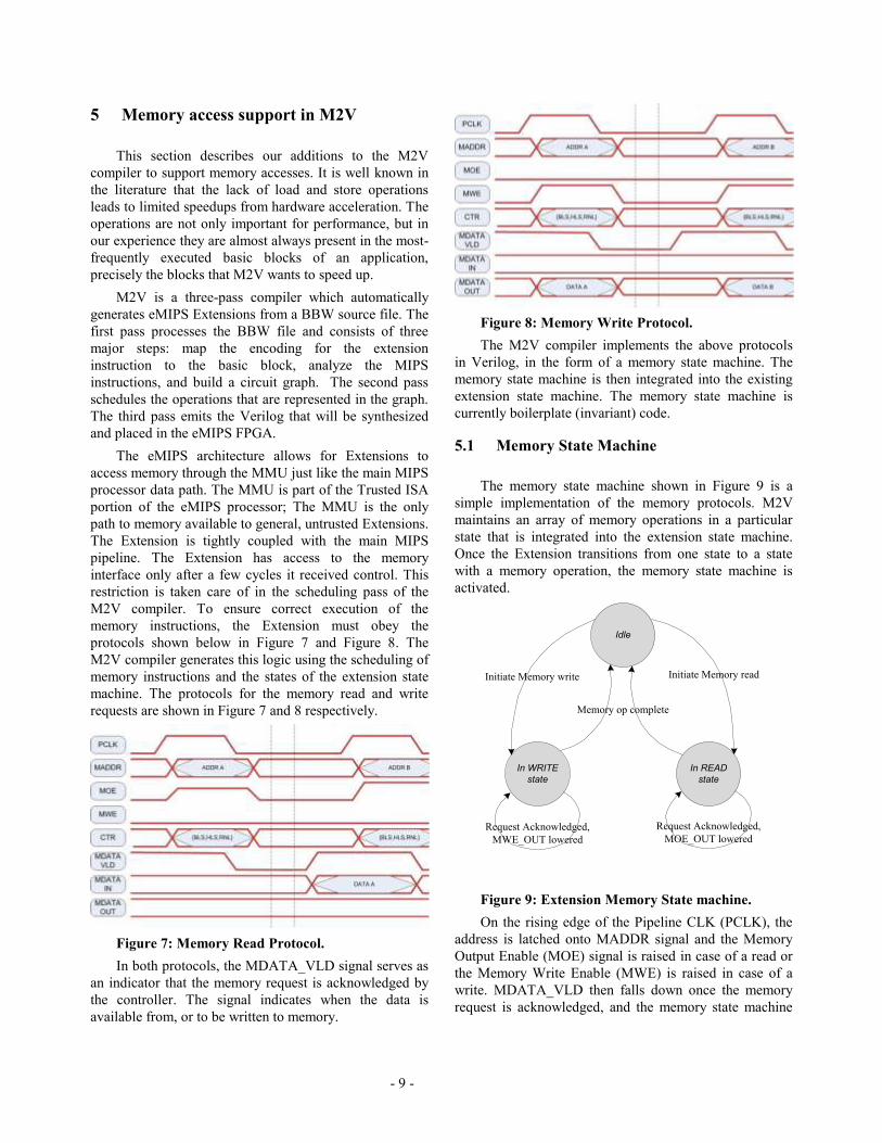
requests are shown in Figure 7 and 8 respectively.
Figure 7: Memory Read Protocol.
In both protocols, the MDATA_VLD signal serves as
an indicator that the memory request is acknowledged by
the controller. The signal indicates when the data is
available from, or to be written to memory.
Figure 8: Memory Write Protocol.
The M2V compiler implements the above protocols
in Verilog, in the form of a memory state machine. The
memory state machine is then integrated into the existing
extension state machine. The memory state machine is
currently boilerplate (invariant) code.
5.1 Memory State Machine
The memory state machine shown in Figure 9 is a
simple implementation of the memory protocols. M2V
maintains an array of memory operations in a particular
state that is integrated into the extension state machine.
Once the Extension transitions from one state to a state
with a memory operation, the memory state machine is
activated.
Idle
In READ
state
In WRITE
state
Initiate Memory read
Request Acknowledged,
MOE_OUT loweredRequest Acknowledged,
MWE_OUT lowered
Memory op complete
Initiate Memory write
Figure 9: Extension Memory State machine.
On the rising edge of the Pipeline CLK (PCLK), the
address is latched onto MADDR signal and the Memory
Output Enable (MOE) signal is raised in case of a read or
the Memory Write Enable (MWE) is raised in case of a
write. MDATA_VLD then falls down once the memory
request is acknowledged, and the memory state machine

- 10 -
moves onto the next state, waiting for the MDATA_VLD
to go high, indicating the availability of the data in
MDATA_IN for a read or completion of the write for a
write operation.
When a state involves a memory access, the main
extension state machine waits on the completion of the
memory state machine and transitions to the next state
when all other operations (ex: register reads, register
writes) for that state are completed.
5.2 Implementation
The set of memory instructions in the basic block are
stored in a separate queue called mmuInstVec in the
Circuit class. mmuInstVec is used to generate the memory
address and memory data for the particular memory
transaction. M2V schedules the memory operations just
like other normal instructions. The register encoding
algorithm described earlier takes care of the necessity to
schedule loads as early as possible in the basic block. The
encoding plays an important part in selecting two critical
paths (of high depth). This will ensure that operations are
executing in parallel to the load instruction, thereby hiding
the latency of the load instruction.
Scheduling of memory operations by M2V is limited
by the number of memory ports available to the Extension.
In the current version, there is a single port available to
the Extension, limiting the number of memory operations
in a state of the Extension to one.
During the scheduling pass, when M2V encounters a
memory instruction it first checks if the memory port has
already been used. In the event that the port has already
been used, the function returns with a RET_FAIL_RSRC
error, indicating resource constraints. The register node
supplying the base address is pipelined to allow access in
the next state of the Extension.
If the memory port is available in the current state, the
compiler proceeds to checking if the required register
reads are already available. Once all the dependencies are
met, the compiler marks the node with the cycle to be
scheduled and updates the counter to reflect the usage of
the memory port in the current state of the Extension.
M2V ensures that the ADDR_OUT/IN and
DATA_OUT/IN pins are correctly MUX’d based on the
instruction stream in the basic block. The M2V compiler
generates a logic block to handle this requirement. If a
basic block consists of more than one memory instruction,
the ADDR_OUT pins must reflect the correct address for
each of the instructions. As mentioned previously, only
one memory operation is allowed in each state of the
extension. Thus the ADDR_OUT/IN and DATA_OUT/IN
pins are determined and MUX’d based on the current state
of the extension.
M2V pipelines the destination register of the memory
instruction to account for the variable latency of the load
instruction node.
6 Interrupt Support
We have modified the M2V compiler to generate
Verilog code with the ability to handle interruptions while
the processor is executing in the Extension. Interruptions
can be due to three different sources, but we will use the
single term “interrupt” to indicate any and all of them. Our
approach handles all cases in the same manner. The first
cause of interrupts is address translation misses and errors
in the MMU while the Extension is trying to access
memory. A second cause is actual interrupts from
peripherals such as timers and I/O devices. A third cause
of interrupts is the case of errors inside the Extension,
such as unaligned addresses and overflows. We use a
transaction model based approach to handle all interrupts
in the Extension.
The basic block to be accelerated is analyzed and
divided into “transactions”. A transaction is a set of
instructions that terminate just before a memory
instruction. Even in the event the basic block has no
memory operations, there is still a maximum number of
cycles allowed before interrupts are permitted. The
maximum number of operations in a particular transaction
is currently fixed at 7. Future work might include taking
into account the actual latency/cost of the instructions
rather than an arbitrary fixed number.
The Extension must correctly indicate to the TISA
what is the re-start address for execution, e.g. after the
software interrupt handler returns. This address is termed
the Virtual PC (VIRPC), as the Extension is keeping track
of the PC as seen by the MIPS pipeline, even though the
Extension has no concept of instruction fetch or
instruction ordering mechanisms. The VIRPC address
simply corresponds to the start of each transaction in the
original basic block.
We illustrate the subdivision of a basic block in
transactions with an example in Figure 10. Transaction 1
terminates once the load instruction ([c]) is encountered.
Transaction 2 is terminated at the end of the maximum
allowed 7 instructions in the transaction. The remaining
instructions are part of transaction 3. The basic idea
behind the transactions scheme is to preserve the original
program order, while at the same time allowing for more
optimistic and more parallel execution inside the
Extension. The Extension will recognize an interrupt at
the next transaction boundary should an interrupt occur

- 11 -
during the Extension’s execution. Any write-backs that are
due to a subsequent transaction are aborted.
[0] sll r1,r1,1
[4] sll r7,r1,2
[8] addu r7,r7,r8
[c] lw r7,0(r7)
[10] srl r3,r2,31
[14] or r1,r1,r3
[18] sll r2,r2,1
[1c] srl r3,r4,31
[20] or r2,r2,r3
[24] sll r4,r4,1
[28] srl r3,r5,31
[2c] or r4,r4,r3
[30] sltu r3,r1,r6
[34] beq r0,r3,4c
[38] sll r5,r5,1
Transaction 1
Transaction 2
Transaction 3
Figure 10: Example basic block illustrating the
concept of transactions.
The transaction model is used to perform write backs
in-order, but from the abstracted viewpoint of a
transaction, that is, the write backs in transaction 1 must
complete prior to any write backs in transaction 2.
However, the write backs inside a particular transaction
can be performed out of order. This limits the parallelism
generated by the circuit graph to some extent by imposing
the restriction of performing certain write backs in order.
We perceive this to not be a huge problem as the eMIPS
TISA interface allows for two register writes every cycle,
thus decreasing the possibility of bottlenecks at the
register file.
[0] sll r1,r1,1
[4] sll r7,r1,2
[8] addu r7,r7,r8
[c] lw r7,0(r7)
[10] srl r3,r2,31
[14] or r1,r1,r3
[18] sll r2,r2,1
[1c] srl r3,r4,31
[20] or r2,r2,r3
[24] sll r4,r4,1
[28] srl r3,r5,31
[2c] or r4,r4,r3
[30] sltu r3,r1,r6
[34] beq r0,r3,4c
[38] sll r5,r5,1
[0] sll r1,r1,1
[4] sll r7,r1,2
[8] addu r7,r7,r8
[c] lw r7,0(r7)
[10] srl r3,r2,31
[14] or r1,r1,r3
[18] sll r2,r2,1
[1c] srl r3,r4,31
[20] or r2,r2,r3
[24] sll r4,r4,1
[28] srl r3,r5,31
[2c] or r4,r4,r3
[30] sltu r3,r1,r6
[34] beq r0,r3,4c
[38] sll r5,r5,1
T1
T2
T3
9 Writebacks to the RF 6 Writebacks to the RF
Transactional Model No interrupt handling
Figure 11: Overhead of handling interrupts.
Figure 11 illustrates the overhead in terms of register
write-backs. In the case of generating hardware without
the support of interrupts only 6 write-backs are necessary
to the register file. It can be clearly seen that further
optimizations can be applied to this basic transaction
model. By just terminating Transaction 2 an instruction
before or after would have reduced the number of write-
backs by 2. This would have ensured only one extra write-
back in the transactional model approach.
M2V adds transactions registers to the Extension to
keep track of the current transaction being written back for
a particular state of the Extension. When the Extension
encounters an interrupt, the extension state machine
checks to see if the current state of the Extension is an end
of a transaction or not. If it is an end of a transaction, the
VIRPC is updated to reflect the address of the start of the
next transaction and the extension state machine is stalled
in that state. The Extension then waits for the resources to
be taken away by the pipeline arbiter and the Enable and
Grant signal to go low. Once the enable goes low, the
Extension lowers the ACK signal to signal the end of the
Extension at that transaction. The program then re-starts
execution from the VIRPC address on the main MIPS
processor, with the registers and other structures in the
correct state.
6.1 Implementation
We added a Transactions class to the M2V. The
Transactions class records the write-backs in a particular
transaction, and the start and end states of the write-backs
for a particular transaction.
Prior to the scheduling pass, M2V determines the
registers that must be written back to the Register File
(RF). If the transaction model is enabled by the M2V user
option, then the Transactions class is populated at this
point with the registers that need to be written back to the
RF. This information is stored in a queue data structure
named writeBacks, as part of the Transactions class. The
start address for each transaction, used as VIRPC, is also
populated at this point.
There is no change in the scheduling of operations in
the transaction model, the only difference being the write-
backs to the RF. For a given state, the compiler first
determines which transaction is currently being written
back. The compiler then iterates through its write-back
queue, regWrVec, to check if there are any pending write
backs for the current transaction, issuing the write-backs
in case of a match. This ensures that write-backs within a
transaction are performed as soon as the values are
available, potentially out-of-order. As part of this
scheduling, the starting state and ending state for write-
backs of a particular transaction are populated in the
Transactions class. This is later used in the Verilog
generating pass of the compiler as part of the extension
state machine.

- 12 -
In the hardware implementation pass, we use a
register array in the Extension to maintain the transaction
information for a particular state of the Extension. This is
generated from the start and end states of the write-backs
as populated in the scheduling pass.
The extension state machine performs in the same
way without interrupts. In the event of an interrupt, the
state machine transitions states only till the end of the
current transaction. Once the end of the transaction is
identified, the extension state machine stalls and does not
perform any more operations/write-backs. This ensures
that the registers and memory are in the correct state to
resume execution at the next transaction PC address.
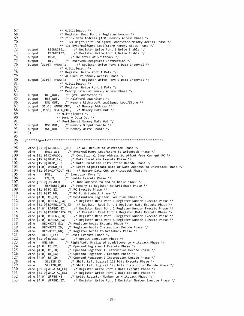
7 Hardware Implementation Details
Appendix III lists the complete Verilog code that
M2V generates for the basic block in Appendix I. There
are four contributions to the final Verilog file: the eMIPS
invariant code, the BBW dependent code, the circuit
graph dependent code, and the cycle dependent code.
Lines 1-580 of the Appendix are the first lines of
eMIPS invariant code in the accelerator definition. Lines
1-340 define the Extension’s top-level module, lines 341-
465 define the bus macros for the execution-to-write-back
interface, and lines 466-580 define the bus macros for the
instruction-decode-to-execution interface. Lines 1-340
are simply copied from m2v_mod_bp.v at runtime.
The Extension’s top-level module defines the
interface signals between the Extension and the rest of the
eMIPS design. It contains multiplexor logic for the shared
data busses to the register file and the program counter
update logic. It also instantiates four modules that make
up the core of the Extension: the instruction decode logic,
the execution logic, and the two bus macro modules.
The bus macros provide connectivity between the
extension logic and the primary eMIPS logic. They
represent physical routing locations and are required for
partial reconfiguration.
The instruction decode logic defined in lines 581-640
is BBW dependent code. This logic decodes the
instruction in parallel with the primary RISC pipeline. If
the opcode of the instruction matches the opcode of the
Extension, the logic will assert the RI signal so that the
extension logic can take control from the RISC pipeline.
The fall-through address for the basic block is sent to the
program counter. The fields within the instruction are
decoded and sent to the execution logic. This version of
M2V hardcodes the extension instruction to the MIPS “I”
format. The Circuit.emit_decode method generates this
code.
The extension execution logic is defined in lines 641-
1311. The execution logic is composed of invariant code,
BBW dependent code, circuit graph dependent code, and
cycle dependent code.
Lines 641-722 define the interface signals between
the execution logic and the rest of eMIPS. The signals are
invariant for every Extension and are copied from
m2v_ex_bp.v at runtime.
Lines 722-767 define the Verilog registers that are
used later in the execution logic. This code is circuit
graph and cycle dependent. The registers for the register
node values follow a convention to create an identifiable
mapping between the generated logic and the circuit
graph. The format is rX_Y[_r], where X is the actual
MIPS register, Y is the sequence number of the register
node, “_r” indicates that the value comes directly from a
register, and the absence of “_r” indicates that the value
comes from combinatorial logic. Thus, r9_3 is a
combinatorial value for MIPS register 9 that corresponds
to the register node with sequence number 3. The
Circuit.emitVarDecl method generates this code.
The last part of the above Verilog block, from 761-
767 is dependent on the transactional model and are
present only if the transactional model is enabled.
Lines 770-1077 define the state machines that
interface with the register file, the program counter logic
and the Memory Management Unit (MMU). This code is
invariant and is copied from m2v_state_mc.v at runtime.
These state machines are eMIPS-specific.
Lines 1113-1176 define the register file, program
counter and memory port usage for each cycle in the
Extension. Additionally, if the transactional model is
enabled, it contains information regarding the progress of
transactions with respect to the cycles in the Extension.
This information is used by the state machines defined in
lines 770-1077. Lines 800-900 define the memory state
machine part of the Extension, as shown in Figure 9. This
code is generated by the Circuit.emitCycState method.
Lines 1080 – 1113 define the transactional model
logic and the state machine used for the transactional
model. Methods Circuit.emitTransactionStateMachine
and Circuit.emitTransactionLogic generate this code.
Lines 1176-1216 define the register file interface
logic. Since there are limited ports on the register file, the
read and write addresses are scheduled onto the register
file address lines. Likewise, read data from the register
file must be routed to the correct register node, and write
data to the register file must come from the correct
calculation. The Circuit.emitRFLogic method generates
this code.
- 13 -
Lines 1220-1240 define the pipeline registers needed
by the extension logic. When a calculation must be
pipelined, it is latched at the end of the calculation cycle
and held for the remainder of the Extension’s execution.
The Circuit.emitPipeReg method generates this code.
Lines 1240-1250 define the logic for generating the
address and data out to the memory for the memory
instruction in the basic block, if any. The
Circuit.emitMemLogic method generates this code.
Lines 1250-1290 define the combinatorial logic for
the instruction nodes. The Circuit.emitInstLogic method
generates this code.
Lines 1290-1311 define the primary extension state
machine. The state machine is 1-hot encoded with one
state representing one cycle in the schedule so the states
can be directly used as control signals. The machine is
idle until an Extension is successfully decoded and it steps
through each state in the Extension. The Circuit.emitESM
method generates this code.
8 Synthesis Reports
Appendix II contains the synthesis reports for three
different versions of the Extension hardware generated for
the same example basic block from Appendix I.
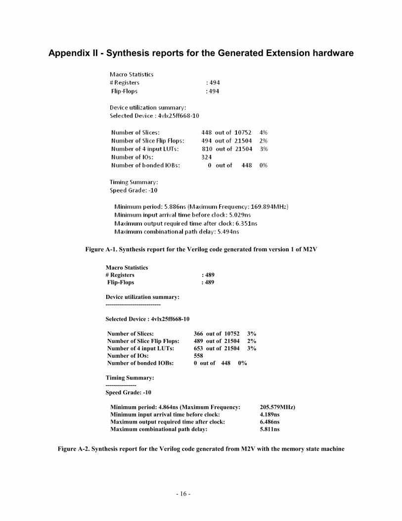
Figure A-1 is the synthesis report for the hardware
generated by M2V without the support for memory
instructions and interrupt handling. This report was
generated on an earlier version of eMIPS, with a different
data path and a different version of the Xilinx ISE tools. It
represents the state of the M2V compiler at the start of the
work described herein.
Figure A-2 is the synthesis report for the design
generated by the current M2V, with the support for
memory instructions but without the interrupt handling
capability. The addition to the design is mainly the
memory state machine logic. The reports show the effects
of the changes in the interfaces to the base data path that
have occurred since the initial release of eMIPS. There is
an approximate 1% reduction in area utilization due
mainly to the simplification of the memory interface. On
the other hand, the interface has grown considerably in
number of signals, as indicated by the number of IOs
parameter.
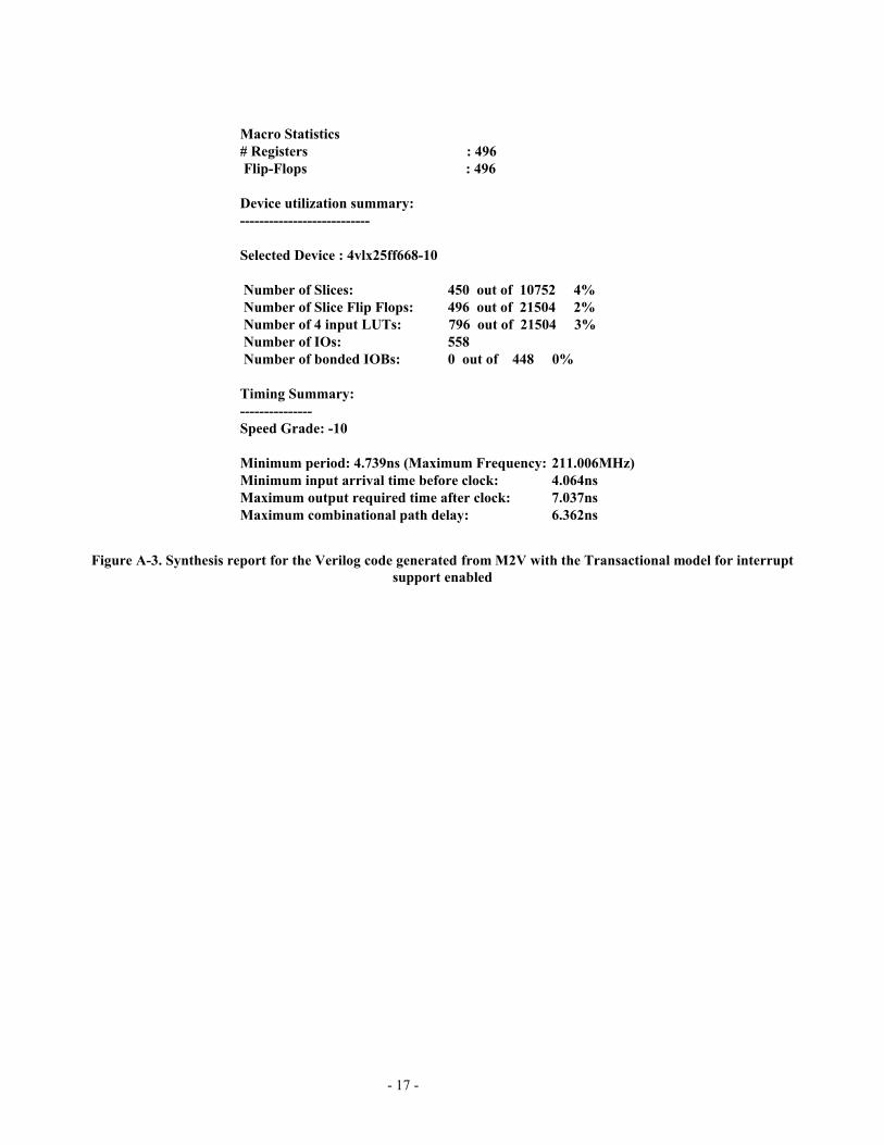
Figure A-3 is for the hardware generated with the
support for both memory operations and interrupts. It can
be seen from the statistics that there are extra registers
used in the case when the transactional model is enabled.
In addition, the percentage of total slices used increases
from 3% to 4%.
Overall, the added complexity from interrupts causes
a penalty in area utilization. This extra cost is balanced
almost exactly by the improvements garnered by the new
data path interfaces. A second improvement is shown in
the maximum frequency of the design, grown from about
170 MHz to about 210 MHz This is also due to the
interface changes.
9 Experimental Results
We tested the changes to the compiler with the
example basic block shown in Figure 6. The basic block is
a 64-bit division block seen in Doom with an extra
memory instruction (load from the stack pointer) inserted
to illustrate the working of memory access through the
instruction. To test interrupt handling, we generated timer
interrupts at short random intervals. The Extension was
simulated using ModelSim and the test program
simulation was run in Giano. The test program checked
over 500 test vectors for the 64-bit division and the test
passed successfully in all cases. The Extension always
reported the correct Virtual PC (VIRPC) address and the
transactional state machine worked as designed. There
was no time left in the internship to test on the actual
boards.
To test for code coverage, we ran the BBMatch and
the M2V compiler on 325 executable files from the code
base of the MMLite RTOS [21]. BBMatch extracted and
encoded about 150,000 blocks from these files. We then
ran the compiler on all the extracted blocks. The results
are shown in Table 1.
Table 1: M2V code coverage test results
No. files 325
No. blocks 146,057 Percent Total
Compiled ok 25,029 17.1%
Warnings 44,800 30.7%
Failure 76,228 52.2%
The large number of failures is actually due in large part
to a small number of unsupported instructions, especially
JAL, BLTZ, BGEZ, MULT, DIV, SLLV, and SRLV.
10 Conclusions
We have modified the eMIPS tool chain to remove
the last remaining obstacles for a fully-automated
generation of hardware accelerators. By supporting load
and stores, interrupts, and the automatic encoding of
extended instructions the compiler can now attack all of
the single-block cases of practical applications. Code

- 14 -
coverage is currently 50% of the blocks in more than 300
executable files, with only a few unsupported instructions
responsible for most of the failures. The addition of
interrupt support to the M2V compiler is especially
relevant because there is now no limit to the span of an
accelerator, even in a general-purpose environment. An
arbitrarily long sequence of instructions can be
accelerated, without concerns for security or real-time
responsiveness.
Support for interrupts in the compiler causes the loss
of a little amount of parallelism, because of the in-order
write-backs requirement. Using a transactional model
mitigates this effect. The ability to perform two write-
backs to the register file in every cycle of the Extension
further mitigates this effect. The overhead of transactions
would be minimal in the case of large basic blocks with a
large number of extension states.
In future revisions of M2V, optimization algorithms
can be implemented to combine certain transactions to
minimize the amount of write-backs and reduce the
pressure on the register file.
Support for branches will have to be tested in the next
revision of M2V. The framework used for supporting
branches should be the same framework used for
interrupts. A (conditional) branch can be considered as
simply terminating a transaction.
References
[ 1 ] Aho, A. V.., Lam, M. S., Sethi, R., Ullman, J. D.
Compilers: Principles, Techniques, and Tools.
Addison Wesley Publishers, Boston, MA. 2007.
[ 2 ] Almeida, O., et al. Embedded Systems Research at
DemoFest’07. Microsoft Research Technical Report
MSR-TR-2007-94, July 2007.
[ 3 ] Altera Corp. Excalibur Embedded Processor
Solutions, 2005. .http://www.altera.com/products/devices/excalibur/excindex.html,
[ 4 ] Biswas, P., Banerjee, S., Dutt, N., Ienne, P., Pozzi, L.
Performance and Energy Benefits of Instruction Set
Extensions in an FPGA Soft Core VLSID’06, pag.
651-656
[ 5 ] Bonzini, P., Pozzi, L. Code Transformation
Strategies for Extensible Embedded Processors
CASES’06, pagg. 242-252.
[ 6 ] Forin, A., Lynch, N., L., Pittman, R. N. eMIPS,A
Dynamically Extensible Processor. Microsoft
Research Technical Report MSR-TR-2006-143,
October 2006.
[ 7 ] Hauck, S. et al. The Chimaera Reconfigurable
Functional Unit. IEEE VLSI, 2004.
[ 8 ] Hauser, J. R., Wawrzynek, J. Garp: A MIPS
Processor with a Reconfigurable Coprocessor.
FCCM’97 pagg 12-21, April 1997.
[ 9 ] Hennessy, J. L., Patterson, D.A. Computer
Organization and Design: The Hardware/Software
Interface. Morgan Kaufmann Publishers, San
Francisco, CA. 1998.
[ 10 ] Kane, G., Heinrich, J. MIPS RISC Architecture.
Prentice Hall, Upper Saddle River, NJ. 1992.
[ 11 ] Kastner, R., Kaplan, A., Ogrenci Memik, S.
Bozorgzadeh, E. Instruction generation for hybrid
reconfigurable systems TODAES vol. 7, no. 4, pagg.
605-632, October 2002.
[ 12 ] Lau, D., Pritchard, O., Molson, P. Automated
Generation of Hardware Accelerators with Direct
Memory Access from ANSI/ISO Standard C
Functions. FCCM’06, pagg. 45-54, April 2006.
[ 13 ] Stretch, Inc. http://www.stretchinc.com 2006.
[ 14 ] Tensilica, Inc. http://www.tensilica.com, 2006.
[ 15 ] Xilinx Inc. Virtex 4 Family Overview. Xilinx Inc.,
June 2005. Available at
http://direct.xilinx.com/bvdocs/publications/ds112.pdf [ 16 ] Meier, K., Forin, A. MIPS-to-Verilog, Hardware
Compilation for the eMIPS Processor, MSR-TR-
2007-128, Microsoft Research, WA, September 2007.
[ 17 ] Mittal, G., Zaretsky, D.C., Xiaoyong Tang,
Banerjee, P. Automatic translation of software
binaries onto FPGAs Design Automation Conference,
2004. Proceedings. 41st
[ 18 ] Mittal, G., Zaretsky, D.C., Xiaoyong Tang,
Banerjee, P. An overview of a compiler for mapping
software binaries to hardware IEEE VLSI, 2007.
[19] Chandrasekhar, V., Forin, A. Mining Sequential
Programs for Coarse-grained Parallelism using
Virtualization, MSR-TR-2008-113, Microsoft
Research, WA, August 2008.
[ 20 ] Available at
http://research.microsoft.com/research/msagl/
[21] Available at http://research.microsoft.com/invisible/
[22] Available at
http://research.microsoft.com/research/EmbeddedSyst
ems/Giano/giano.aspx

- 15 -
Appendix I – BBW File for Example Basic Block
[bbname __ull_div]
MIPSBE
[encoding]
[r1=r2+1;r3=r0+11;r5=r4+1;r6=r5+1]b26.6:c011110;b21.5:r4;b16.5:r2;b0.16:v0;
[code 48]
40080100
c21f0200
25082300
40100200
c21f0400
25104300
40200400
c21f0500
25208300
2b182600
5000310
40280500
[disasm]
sll r1,r1,1
srl r3,r2,31
or r1,r1,r3
sll r2,r2,1
srl r3,r4,31
or r2,r2,r3
sll r4,r4,1
srl r3,r5,31
or r4,r4,r3
sltu r3,r1,r6
beq r0,r3,40
sll r5,r5,1
[registers 7]
0,9,8,11,4,5,6
[valuess 1]
{40,11,5}
- 16 -
Appendix II - Synthesis reports for the Generated Extension hardware
Figure A-1. Synthesis report for the Verilog code generated from version 1 of M2V
Macro Statistics
# Registers : 489
Flip-Flops : 489
Device utilization summary:
---------------------------
Selected Device : 4vlx25ff668-10
Number of Slices: 366 out of 10752 3%
Number of Slice Flip Flops: 489 out of 21504 2%
Number of 4 input LUTs: 653 out of 21504 3%
Number of IOs: 558
Number of bonded IOBs: 0 out of 448 0%
Timing Summary:
---------------
Speed Grade: -10
Minimum period: 4.864ns (Maximum Frequency: 205.579MHz)
Minimum input arrival time before clock: 4.189ns
Maximum output required time after clock: 6.486ns
Maximum combinational path delay: 5.811ns
Figure A-2. Synthesis report for the Verilog code generated from M2V with the memory state machine
- 17 -
Macro Statistics
# Registers : 496
Flip-Flops : 496
Device utilization summary:
---------------------------
Selected Device : 4vlx25ff668-10
Number of Slices: 450 out of 10752 4%
Number of Slice Flip Flops: 496 out of 21504 2%
Number of 4 input LUTs: 796 out of 21504 3%
Number of IOs: 558
Number of bonded IOBs: 0 out of 448 0%
Timing Summary:
---------------
Speed Grade: -10
Minimum period: 4.739ns (Maximum Frequency: 211.006MHz)
Minimum input arrival time before clock: 4.064ns
Maximum output required time after clock: 7.037ns
Maximum combinational path delay: 6.362ns
Figure A-3. Synthesis report for the Verilog code generated from M2V with the Transactional model for interrupt
support enabled

- 18 -
Appendix III – Verilog Output for the Example Basic Block 1
2 // a.v 3 // auto-generated by m2v revision 1 on Fri Aug 15 15:46:50 2008 4 // 5 // INFO: reading from m2v_mod_bp.v 6 // 7 // m2v_mod_bp.v 8 // 8/15/07 9 // Karl Meier, Neil Pittman 10 // 11 // MIPS to Verilog (m2v) module (_mod) boilerplate (_bp) 12 // 13 // Copyright (c) Microsoft Corporation. All rights reserved. 14 15 `timescale 1ns / 1ps 16 17 module mmlite_div64 ( 18 /*****Ports****************************************************************/ 19 /* INPUT PORTS */ 20 input CLK, /* System Clock 50 - 100 MHZ */ 21 input EN, /* Enable */ 22 input EXCEXT, /* Exception Flush */ 23 input EXTNOP_MA, /* Extension Bubble in Memory Access Phase */ 24 input GR, /* Grant Pipeline Resources */ 25 input [31:0] INSTR, /* Current Instruction */ 26 input [31:0] PC, /* Current PC External */ 27 input PCLK, /* Pipeline Clock */ 28 input [31:0] RDREG1DATA, /* Register Read Port 1 Register Data */ 29 input [31:0] RDREG2DATA, /* Register Read Port 2 Register Data */ 30 input [31:0] RDREG3DATA, /* Register Read Port 3 Register Data */ 31 input [31:0] RDREG4DATA, /* Register Read Port 4 Register Data */ 32 input REGEMPTY, /* Register Write Buffer Empty */ 33 input REGFULL, /* Register Write Buffer Full */ 34 input REGRDY, /* Register Write Buffer Ready */ 35 input RESET, /* System Reset */ 36 input [31:0] MDATA_IN, /* Memory Data In */ 37 /* Multiplexed: */ 38 /* Memory Data In */ 39 /* Peripheral Memory Data In */ 40 /* Memory Data Monitor */ 41 input MDATA_VLD_IN, /* Memory Data Valid */ 42 43 /* OUTPUT PORTS */ 44 output ACK, /* Enable Acknowledged */ 45 output [31:0] EXTADD, /* Extension Address */ 46 /* Multiplexed: */ 47 /* Next PC */ 48 /* Exception Address */ 49 /* PC Memory Access Phase */ 50 output PCNEXT, /* Conditional PC Update */ 51 output [4:0] RDREG1, /* Register Read Port 1 Register Number */ 52 /* Multiplexed: */ 53 /* Register Read Port 1 Register Number */ 54 /* Register Write Port 1 Register Number */ 55 /* Write Register Memory Access Phase */ 56 output [4:0] RDREG2, /* Register Read Port 2 Register Number */ 57 /* Multiplexed: */ 58 /* Register Read Port 2 Register Number */ 59 /* Register Write Port 2 Register Number */ 60 /* <0> Register Write Enable Memory Access Phase */ 61 /* <1> Memory to Register Memory Acess Phase */ 62 output [4:0] RDREG3, /* Register Read Port 3 Register Number */ 63 /* Multiplexed: */ 64 /* Register Read Port 3 Register Number */ 65 output [4:0] RDREG4, /* Register Read Port 4 Register Number Internal */ 66
- 19 -
/* Multiplexed: */ 67 /* Register Read Port 4 Register Number */ 68 /* <1:0> Data Address [1:0] Memory Access Phase */ 69 /* <2> Right/Left Unaligned Load/Store Memory Access Phase */ 70 /* <3> Byte/Halfword Load/Store Memory Acess Phase */ 71 output REGWRITE1, /* Register Write Port 1 Write Enable */ 72 output REGWRITE2, /* Register Write Port 2 Write Enable */ 73 output REWB, /* Re-enter at Writeback */ 74 output RI, /* Reserved/Recognized Instruction */ 75 output [31:0] WRDATA1, /* Register Write Port 1 Data Internal */ 76 /* Multiplexed: */ 77 /* Register Write Port 1 Data */ 78 /* ALU Result Memory Access Phase */ 79 output [31:0] WRDATA2, /* Register Write Port 2 Data Internal */ 80 /* Multiplexed: */ 81 /* Register Write Port 2 Data */ 82 /* Memory Data Out Memory Access Phase */ 83 output BLS_OUT, /* Byte Load/Store */ 84 output HLS_OUT, /* Halfword Load/Store */ 85 output RNL_OUT, /* Memory Right/Left Unaligned Load/Store */ 86 output [31:0] MADDR_OUT, /* Memory Address */ 87 output [31:0] MDATA_OUT, /* Memory Data Out */ 88 /* Multiplexed: */ 89 /* Memory Data Out */ 90 /* Peripheral Memory Data Out */ 91 output MOE_OUT, /* Memory Output Enable */ 92 output MWE_OUT /* Memory Write Enable */ 93 ); 94 95 /*****Signals****************************************************************/ 96 97 wire [31:0] ALURESULT_WB; /* ALU Result to Writeback Phase */ 98 wire BHLS_WB; /* Byte/Halfword Load/Store to Writeback Phase */ 99 wire [31:0] CJMPADD; /* Conditional Jump address to offset from Current PC */ 100 wire [15:0] DIMM_EX; /* Data Immediate Execute Phase */ 101 wire [15:0] DIMM_ID; /* Data Immediate Instruction Decode Phase */ 102 wire [1:0] DMADD_WB; /* Least Significant Bits of Data Address to Writeback Phase */ 103 wire [31:0] DMDATAOUT_WB; /* Memory Data Out to Writeback Phase */ 104 wire DNE; /* Execution Done */ 105 wire EN_EX; /* Enable Execute Phase */ 106 wire [31:0] JMPADD; /* Jump address to end of basic block */ 107 wire MEMTOREG_WB; /* Memory to Register to Writeback Phase */ 108 wire [31:0] PC_EX; /* PC Execute Phase */ 109 wire [31:0] PC_WB; /* PC to Writeback Phase */ 110 wire [4:0] RD_EX; /* Destination Register Execution Phase */ 111 wire [4:0] RDREG1_EX; /* Register Read Port 1 Register Number Execute Phase */ 112 wire [31:0] RDREG1DATA_EX; /* Register Read Port 1 Register Data Execute Phase */ 113 wire [4:0] RDREG2_EX; /* Register Read Port 2 Register Number Execute Phase */ 114 wire [31:0] RDREG2DATA_EX; /* Register Read Port 2 Register Data Execute Phase */ 115 wire [4:0] RDREG3_EX; /* Register Read Port 3 Register Number Execute Phase */ 116 wire [4:0] RDREG4_EX; /* Register Read Port 4 Register Number Execute Phase */ 117 wire REGWRITE_EX; /* Register Write Execute Phase */ 118 wire REGWRITE_ID; /* Register Write Instruction Decode Phase */ 119 wire REGWRITE_WB; /* Register Write to Writeback Phase */ 120 wire RESET_EX; /* Reset Execute Phase */ 121 wire [31:0] RESULT_EX; /* Result Execution Phase */ 122 wire RNL_WB; /* Right/Left Unaligned Load/Store to Writeback Phase */ 123 wire [4:0] RS_EX; /* Operand Register 1 Execute Phase */ 124 wire [4:0] RS_ID; /* Operand Register 1 Instruction Decode Phase */ 125 wire [4:0] RT_EX; /* Operand Register 2 Execute Phase */ 126 wire [4:0] RT_ID; /* Operand Register 2 Instruction Decode Phase */ 127 wire SLL128_EX; /* Shift Left Logical 128 bits Execute Phase */ 128 wire SLL128_ID; /* Shift Left Logical 128 bits Instruction Decode Phase */ 129 wire [31:0] WRDATA1_EX; /* Register Write Port 1 Data Execute Phase */ 130 wire [31:0] WRDATA2_EX; /* Register Write Port 2 Data Execute Phase */ 131 wire [4:0] WRREG_WB; /* Write Register Number to Writeback Phase */ 132 wire [4:0] WRREG1_EX; /* Register Write Port 1 Register Number Execute Phase */ 133

- 20 -
wire [4:0] WRREG2_EX; /* Register Write Port 2 Register Number Execute Phase */ 134 wire [31:0] VIRPC; 135 136 /*****Registers****************************************************************/ 137 138 reg en_reg; /* Enable */ 139 reg gr_reg; /* Grant Pipeline Resources */ 140 141 /*****Initialization****************************************************************/ 142 /* 143 initial 144 begin 145 en_reg = 1'b0; 146 gr_reg = 1'b0; 147 end 148 */ 149 150 /*********************************************************************/ 151 152 assign EXTADD = (EXCEXT)? VIRPC: 153 (en_reg)? JMPADD: 154 (PCNEXT)? CJMPADD: 155 (REWB)? PC_WB: 156 32'hffffffff; 157 /* 158 * The rest cannot be zero'ed out as the extension state machine 159 * might still have to be completed till a particular transaction ends 160 */ 161 assign RDREG1 = (gr_reg & REGWRITE1)? WRREG1_EX: 162 //(EXCEXT)? 5'b0: 163 (REWB & gr_reg)? WRREG_WB: 164 (gr_reg)? RDREG1_EX: 165 5'b11111; 166 assign RDREG2 = (gr_reg & REGWRITE2)? WRREG2_EX: 167 //(EXCEXT)? 5'b0: 168 (REWB & gr_reg)? {3'b0,MEMTOREG_WB,REGWRITE_WB}: 169 (gr_reg)? RDREG2_EX: 170 5'b11111; 171 assign RDREG3 = (REWB & gr_reg)? 5'b0: 172 //(EXCEXT)? 5'b0: 173 (gr_reg)? RDREG3_EX: 174 5'b11111; 175 assign RDREG4 = (REWB & gr_reg)? {1'b0,BHLS_WB,RNL_WB,DMADD_WB}: 176 //(EXCEXT)? 5'b0: 177 (gr_reg)? RDREG4_EX: 178 5'b11111; 179 assign WRDATA1 = (gr_reg & REGWRITE1)? WRDATA1_EX: 180 //(EXCEXT)? 32'b0: 181 (REWB)? ALURESULT_WB: 182 32'hffffffff; 183 assign WRDATA2 = (gr_reg & REGWRITE2)? WRDATA2_EX: 184 //(EXCEXT)? 32'b0: 185 (REWB)? DMDATAOUT_WB: 186 32'hffffffff; 187 188 189 // 190 // instantiate the instruction decode module for the extension instruction 191 // - the instruction decode module is auto generated and appended to the 192 // end of the verilog file (a.v unless redefined) 193 // 194 195 ext_id id ( 196 .CLK(CLK), 197 .DIMM(DIMM_ID), 198 .EN(EN), 199 .JMPADD(JMPADD), 200

- 21 -
.INSTR(INSTR), 201 .PC(PC), 202 .REGWRITE(REGWRITE_ID), 203 .RESET(RESET), 204 .RI(RI), 205 .RS(RS_ID), 206 .RT(RT_ID), 207 .SLL128(SLL128_ID) 208 ); 209 210 /*****Instruction Decode -> Execute****************************************************************/ 211 212 mmldiv64_toex to_ex( 213 .ACK(ACK), 214 .CLK(CLK), 215 .DIMM_EX(DIMM_EX), 216 .DIMM_ID(DIMM_ID), 217 .EN_EX(EN_EX), 218 .EN_ID(EN), 219 .EXCEXT(EXCEXT), 220 .PC_EX(PC_EX), 221 .PC_ID(PC), 222 .PCLK(PCLK), 223 .RDREG1DATA_EX(RDREG1DATA_EX), 224 .RDREG1DATA_ID(RDREG1DATA), 225 .RDREG2DATA_EX(RDREG2DATA_EX), 226 .RDREG2DATA_ID(RDREG2DATA), 227 .REGWRITE_EX(REGWRITE_EX), 228 .REGWRITE_ID(REGWRITE_ID), 229 .RESET(RESET), 230 .RESET_EX(RESET_EX), 231 .RS_EX(RS_EX), 232 .RS_ID(RS_ID), 233 .RT_EX(RT_EX), 234 .RT_ID(RT_ID), 235 .SLL128_ID(SLL128_ID), 236 .SLL128_EX(SLL128_EX) 237 ); 238 239 240 // 241 // instantiate the execution module for the extension instruction 242 // - the execution module is auto generated and appended to the 243 // end of the verilog file (a.v unless redefined) 244 // 245 246 ext_ex ex( 247 .ACK(ACK), 248 .DIMM(DIMM_EX), 249 .DNE(DNE), 250 .CLK(CLK), 251 .CJMPADD(CJMPADD), 252 .EN(EN_EX), 253 .EXTNOP_MA(EXTNOP_MA), 254 .GR(GR), 255 .PC(PC_EX), 256 .PCLK(PCLK), 257 .PCNEXT(PCNEXT), 258 .RD(RD_EX), 259 .RDREG1(RDREG1_EX), 260 .RDREG1DATA(RDREG1DATA), 261 .RDREG1DATA_ID(RDREG1DATA_EX), 262 .RDREG2(RDREG2_EX), 263 .RDREG2DATA(RDREG2DATA), 264 .RDREG2DATA_ID(RDREG2DATA_EX), 265 .RDREG3(RDREG3_EX), 266 .RDREG3DATA(RDREG3DATA), 267
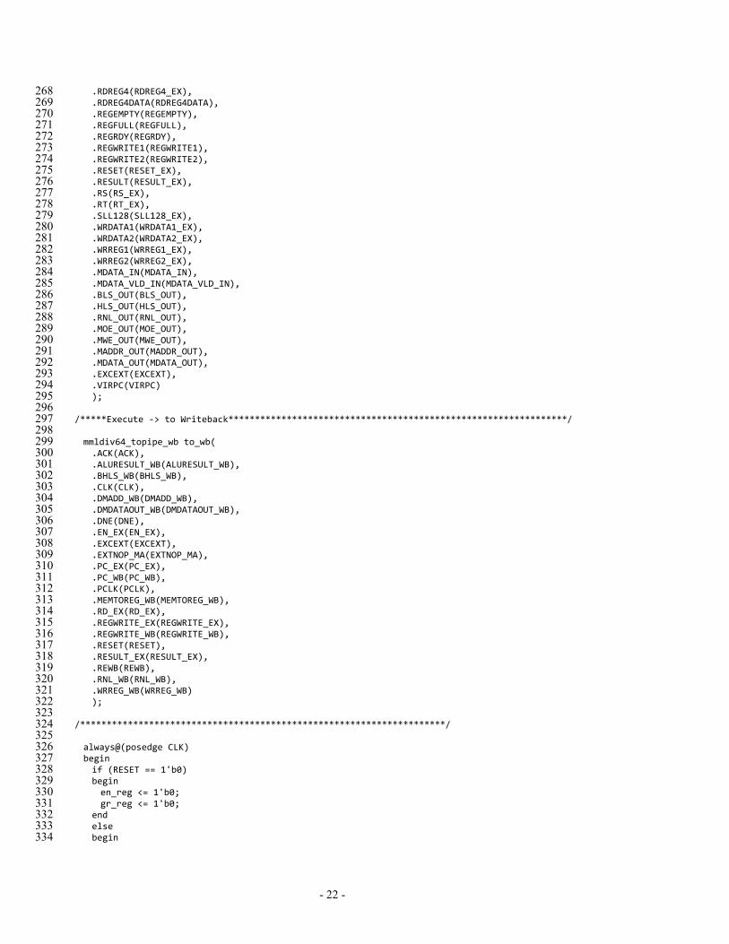
- 22 -
.RDREG4(RDREG4_EX), 268 .RDREG4DATA(RDREG4DATA), 269 .REGEMPTY(REGEMPTY), 270 .REGFULL(REGFULL), 271 .REGRDY(REGRDY), 272 .REGWRITE1(REGWRITE1), 273 .REGWRITE2(REGWRITE2), 274 .RESET(RESET_EX), 275 .RESULT(RESULT_EX), 276 .RS(RS_EX), 277 .RT(RT_EX), 278 .SLL128(SLL128_EX), 279 .WRDATA1(WRDATA1_EX), 280 .WRDATA2(WRDATA2_EX), 281 .WRREG1(WRREG1_EX), 282 .WRREG2(WRREG2_EX), 283 .MDATA_IN(MDATA_IN), 284 .MDATA_VLD_IN(MDATA_VLD_IN), 285 .BLS_OUT(BLS_OUT), 286 .HLS_OUT(HLS_OUT), 287 .RNL_OUT(RNL_OUT), 288 .MOE_OUT(MOE_OUT), 289 .MWE_OUT(MWE_OUT), 290 .MADDR_OUT(MADDR_OUT), 291 .MDATA_OUT(MDATA_OUT), 292 .EXCEXT(EXCEXT), 293 .VIRPC(VIRPC) 294 ); 295 296 /*****Execute -> to Writeback****************************************************************/ 297 298 mmldiv64_topipe_wb to_wb( 299 .ACK(ACK), 300 .ALURESULT_WB(ALURESULT_WB), 301 .BHLS_WB(BHLS_WB), 302 .CLK(CLK), 303 .DMADD_WB(DMADD_WB), 304 .DMDATAOUT_WB(DMDATAOUT_WB), 305 .DNE(DNE), 306 .EN_EX(EN_EX), 307 .EXCEXT(EXCEXT), 308 .EXTNOP_MA(EXTNOP_MA), 309 .PC_EX(PC_EX), 310 .PC_WB(PC_WB), 311 .PCLK(PCLK), 312 .MEMTOREG_WB(MEMTOREG_WB), 313 .RD_EX(RD_EX), 314 .REGWRITE_EX(REGWRITE_EX), 315 .REGWRITE_WB(REGWRITE_WB), 316 .RESET(RESET), 317 .RESULT_EX(RESULT_EX), 318 .REWB(REWB), 319 .RNL_WB(RNL_WB), 320 .WRREG_WB(WRREG_WB) 321 ); 322 323 /*********************************************************************/ 324 325 always@(posedge CLK) 326 begin 327 if (RESET == 1'b0) 328 begin 329 en_reg <= 1'b0; 330 gr_reg <= 1'b0; 331 end 332 else 333 begin 334
- 23 -
en_reg <= EN; 335 gr_reg <= GR; 336 end 337 end 338 339 endmodule 340 341 342 343 /*****Execute -> to Writeback****************************************************************/ 344 345 module mmldiv64_topipe_wb( 346 /*****Ports****************************************************************/ 347 /* INPUT PORTS */ 348 input ACK, /* Enable Acknowledged */ 349 input CLK, /* System Clock 50 - 100 MHZ */ 350 input DNE, /* Execution Done */ 351 input EN_EX, /* Enable Execute Phase */ 352 input EXCEXT, /* Exception Flush */ 353 input EXTNOP_MA, /* Extension Bubble in Memory Access Phase */ 354 input [31:0] PC_EX, /* Current PC Execute Phase */ 355 input PCLK, /* Pipeline Clock */ 356 input [4:0] RD_EX, /* Destination Register Execution Phase */ 357 input REGWRITE_EX, /* Register Write Execute Phase */ 358 input RESET, /* System Reset */ 359 input [31:0] RESULT_EX, /* Result Execution Phase */ 360 /* OUTPUT PORTS */ 361 output [31:0] ALURESULT_WB, /* ALU Result to Writeback Phase */ 362 output BHLS_WB, /* Byte/Halfword Load/Store to Writeback Phase */ 363 output [1:0] DMADD_WB, /* Least Significant Bits of Data Address to Writeback Phase */ 364 output [31:0] DMDATAOUT_WB, /* Memory Data Out to Writeback Phase */ 365 output MEMTOREG_WB, /* Memory to Register to Writeback Phase */ 366 output [31:0] PC_WB, /* Current PC to Writeback Phase */ 367 output REGWRITE_WB, /* Register Write to Writeback Phase */ 368 output REWB, /* Re-enter at Writeback */ 369 output RNL_WB, /* Right/Left Unaligned Load/Store to Writeback Phase */ 370 output [4:0] WRREG_WB /* Write Register Number to Writeback Phase */ 371 ); 372 373 /*****Signals****************************************************************/ 374 375 wire EN_WB; /* Enable to Writeback Phase */ 376 wire RESET_WB; /* Reset to Writeback Phase */ 377 378 /*****Registers****************************************************************/ 379 380 reg [70:0] ex_wb; /* Execute -> to Writeback Pipeline Register */ 381 reg [1:0] pclkcnt; /* Pipeline Clock edge detection */ 382 reg reset_reg; /* Reset to Writeback Phase */ 383 reg rewb_reg; /* Re-enter at Writeback */ 384 385 /*****Initialization****************************************************************/ 386 /* 387 initial 388 begin 389 ex_wb = 71'b0; 390 pclkcnt = 2'b0; 391 rewb_reg = 1'b0; 392 reset_reg = 1'b0; 393 end 394 */ 395 /*********************************************************************/ 396 397 assign RESET_WB = reset_reg; 398 assign REWB = rewb_reg & EN_WB; 399 assign EN_WB = ex_wb[70]; //EN_EX; 400 assign REGWRITE_WB = ex_wb[69]; //REGWRITE_EX; 401

- 24 -
assign MEMTOREG_WB = 1'b0; 402 assign RNL_WB = 1'b0; 403 assign BHLS_WB = 1'b0; 404 assign DMADD_WB = 2'b0; 405 assign WRREG_WB = ex_wb[68:64]; //RD_EX; 406 assign ALURESULT_WB = ex_wb[63:32]; //RESULT_EX; 407 assign DMDATAOUT_WB = 32'b0; 408 assign PC_WB = ex_wb[31:0]; //PC_EX; 409 410 /*********************************************************************/ 411 412 always@(posedge CLK) 413 begin 414 /* Pipeline Clock edge detection */ 415 pclkcnt = {pclkcnt[0],PCLK}; // karl, 9/19, change to non-blocking to 416 // match Neil 417 end 418 419 always@(posedge CLK) 420 begin 421 case(pclkcnt) 422 2'b01 : begin 423 /* Synchronize Reset to Pipeline Clock */ 424 reset_reg <= RESET; 425 end 426 default : begin 427 end 428 endcase 429 end 430 431 always@(posedge CLK) 432 begin 433 /* Execute -> to Memory Access Pipeline Register */ 434 casex({pclkcnt,RESET_WB,EXTNOP_MA,rewb_reg,ACK,DNE,EXCEXT}) 435 8'bxx0xxxxx : begin 436 /* Reset */ 437 rewb_reg <= 1'b0; 438 ex_wb <= 71'b0; 439 end 440 8'b011xxxx1 : begin 441 /* Exception in Pipeline, Flush */ 442 rewb_reg <= 1'b0; 443 ex_wb <= 71'b0; 444 end 445 8'bxx1x0110 : begin 446 /* Latch Data and Control after Execution Finishes */ 447 ex_wb <= {EN_EX,REGWRITE_EX,RD_EX,RESULT_EX,PC_EX}; 448 end 449 8'b101100x0 : begin 450 /* Raise REWB at next Negedge of PCLK after ACK Lowers */ 451 rewb_reg <= 1'b1; 452 end 453 8'b011x1xx0 : begin 454 /* Lower REWB at next Posedge and reset register */ 455 rewb_reg <= 1'b0; 456 ex_wb <= 71'b0; 457 end 458 default : begin 459 /* NOP */ 460 end 461 endcase 462 end 463 endmodule 464 465 466 /*****Instruction Decode -> Execute****************************************************************/ 467 468
- 25 -
module mmldiv64_toex( 469 /*****Ports****************************************************************/ 470 /* INPUT PORTS */ 471 input ACK, /* Enable Acknowledged */ 472 input CLK, /* System Clock 50 - 100 MHZ */ 473 input [15:0] DIMM_ID, /* Data Immediate Instruction Decode Phase */ 474 input EN_ID, /* Enable Instruction Decode Phase */ 475 input EXCEXT, /* Exception Flush */ 476 input [31:0] PC_ID, /* Current PC Decode Phase */ 477 input PCLK, /* Pipeline Clock */ 478 input [31:0] RDREG1DATA_ID, /* Register Read Port 1 Register Data Instruction Decode Phase */ 479 input [31:0] RDREG2DATA_ID, /* Register Read Port 2 Register Data Instruction Decode Phase */ 480 input REGWRITE_ID, /* Register Write Instruction Decode Phase*/ 481 input RESET, /* System Reset */ 482 input [4:0] RS_ID, /* Operand Register 1 Instruction Decode Phase */ 483 input [4:0] RT_ID, /* Operand Register 2 Instruction Decode Phase */ 484 input SLL128_ID, /* Shift Left Logical 128 bits Instruction Decode Phase */ 485 /* OUTPUT PORTS */ 486 output [15:0] DIMM_EX, /* Data Immediate Execute Phase */ 487 output EN_EX, /* Enable Execute Phase */ 488 output [31:0] PC_EX, /* Current PC Instruction Decode Phase */ 489 output [31:0] RDREG1DATA_EX, /* Register Read Port 1 Register Data Execute Phase */ 490 output [31:0] RDREG2DATA_EX, /* Register Read Port 2 Register Data Execute Phase */ 491 output REGWRITE_EX, /* Register Write Execute Phase*/ 492 output RESET_EX, /* Reset Execute Phase */ 493 output [4:0] RS_EX, /* Operand Register 1 Execute Phase */ 494 output [4:0] RT_EX, /* Operand Register 2 Execute Phase */ 495 output SLL128_EX /* Shift Left Logical 128 bits Execute Phase */ 496 ); 497 498 /*****Registers****************************************************************/ 499 500 reg [124:0] id_ex; /* Instruction Decode -> Execute Pipeline Register */ 501 reg [1:0] pclkcnt; /* Pipeline Clock edge detection */ 502 reg reset_reg; /* Reset Execute Phase */ 503 504 /*****Initialization****************************************************************/ 505 506 /* 507 initial 508 begin 509 id_ex = 125'b0; 510 pclkcnt = 2'b0; 511 reset_reg = 1'b0; 512 end 513 */ 514 515 /*********************************************************************/ 516 517 assign RESET_EX = reset_reg; 518 assign EN_EX = id_ex[124]; //EN_ID; 519 assign SLL128_EX = id_ex[123]; //SLL128_ID; 520 assign REGWRITE_EX = id_ex[122]; //REGWRITE_ID; 521 assign RS_EX = id_ex[121:117]; //RS_ID; 522 assign RT_EX = id_ex[116:112]; //RT_ID; 523 assign DIMM_EX = id_ex[111:96]; //DIMM_ID; 524 assign PC_EX = id_ex[95:64]; //PC_ID; 525 assign RDREG1DATA_EX = id_ex[63:32]; //RDREG1DATA_ID; 526 assign RDREG2DATA_EX = id_ex[31:0]; //RDREG2DATA_ID 527 528 /*********************************************************************/ 529 530 always@(posedge CLK) 531 begin 532 /* Pipeline Clock edge detection */ 533 pclkcnt = {pclkcnt[0],PCLK}; // karl, 9/19, change to non-blocking to 534 // match Neil 535

- 26 -
end 536 537 always@(posedge CLK) 538 begin 539 case(pclkcnt) 540 2'b01 : begin 541 /* Synchronize Reset to Pipeline Clock */ 542 reset_reg <= RESET; 543 end 544 default : begin 545 end 546 endcase 547 end 548 549 always@(posedge CLK) 550 begin 551 /* Instruction Decode -> Execute Pipeline Register */ 552 casex({pclkcnt,RESET_EX,ACK,EXCEXT}) 553 5'bxx0xx : begin 554 /* Reset */ 555 id_ex <= 109'b0; 556 end 557 5'b011x1 : begin 558 /* Exception in Pipeline, Flush */ 559 id_ex <= 109'b0; 560 end 561 5'bxx110 : begin 562 /* Hold state during Execute Phase */ 563 end 564 5'b01100 : begin 565 /* Clocking the Pipeline */ 566 id_ex <= {EN_ID,SLL128_ID,REGWRITE_ID,RS_ID,RT_ID,DIMM_ID,PC_ID,RDREG1DATA_ID,RDREG2DATA_ID}; 567 end 568 default : begin 569 /* NOP */ 570 end 571 endcase 572 end 573 endmodule 574 575 576 // 577 // INFO: finished reading from m2v_mod_bp.v 578 // 579 580 // 581 // extension instruction decode 582 // 583 module ext_id( 584 input CLK, 585 input EN, 586 input [31:0] INSTR, 587 input [31:0] PC, 588 input RESET, 589 590 output reg [15:0] DIMM, 591 output reg [31:0] JMPADD, 592 output reg REGWRITE, 593 output reg RI, 594 output reg [4:0] RS, 595 output reg [4:0] RT, 596 output reg SLL128 597 ); 598 599 reg [31:0] jmpadd_c; 600 reg en_r; 601 reg [5:0] op_r; 602

- 27 -
reg [31:0] pc_r; 603 reg opcode_match; 604 605 // combinatorial logic for instruction decode 606 always @ (*) begin 607 jmpadd_c = pc_r + 48 + 4; 608 opcode_match = (op_r == 30); 609 end 610 611 // sequential logic for instruction decode 612 always @ (posedge CLK) begin 613 if (!RESET) begin 614 DIMM <= 16'h0; 615 op_r <= 6'h0; 616 RS <= 5'h0; 617 RT <= 5'h0; 618 en_r <= 1'h0; 619 pc_r <= 32'h0; 620 JMPADD <= 32'h0; 621 RI <= 1'h1; 622 SLL128 <= 1'h0; 623 REGWRITE <= 1'h0; 624 end else begin 625 DIMM <= INSTR[15:0]; 626 op_r <= INSTR[31:26]; 627 RS <= INSTR[25:21]; 628 RT <= INSTR[20:16]; 629 en_r <= EN; 630 pc_r <= PC; 631 JMPADD <= jmpadd_c; 632 RI <= ~opcode_match; 633 SLL128 <= en_r & opcode_match; 634 REGWRITE <= en_r & opcode_match; 635 end 636 end 637 endmodule 638 639 // 640 // INFO: reading from m2v_ex_bp.v 641 // 642 // m2v_ex_bp.v 643 // 8/15/07 644 // Karl Meier, Neil Pittman 645 // 646 // MIPS to Verilog (m2v) execution (_ex) boilerplate (_bp) 647 // 648 // Copyright (c) Microsoft Corporation. All rights reserved. 649 // 650 651 module ext_ex ( 652 /*****Ports****************************************************************/ 653 /* INPUT PORTS */ 654 input CLK, /* System Clock 50 - 100 MHZ */ 655 input [15:0] DIMM, /* Data Immediate */ 656 input EN, /* Enable */ 657 input EXTNOP_MA, /* Extension Bubble in Memory Access Phase */ 658 input GR, /* Grant Pipeline Resources */ 659 input [31:0] PC, /* Current PC */ 660 input PCLK, /* Pipeline Clock */ 661 input [31:0] RDREG1DATA, /* Register Read Port 1 Register Data */ 662 input [31:0] RDREG1DATA_ID, /* Register Read Port 1 Register Data Instruction Decode Phase */ 663 input [31:0] RDREG2DATA, /* Register Read Port 2 Register Data */ 664 input [31:0] RDREG2DATA_ID, /* Register Read Port 2 Register Data Instruction Decode Phase */ 665 input [31:0] RDREG3DATA, /* Register Read Port 3 Register Data */ 666 input [31:0] RDREG4DATA, /* Register Read Port 4 Register Data */ 667 input REGEMPTY, /* Register Write Buffer Empty */ 668 input REGFULL, /* Register Write Buffer Full */ 669
- 28 -
input REGRDY, /* Register Write Buffer Ready */ 670 input RESET, /* System Reset */ 671 input [4:0] RS, /* Operand Register 1 */ 672 input [4:0] RT, /* Operand Register 2 */ 673 input SLL128, /* Shift Left Logical 128 bits */ 674 input [31:0] MDATA_IN, /* Memory Data In */ 675 /* Multiplexed: */ 676 /* Memory Data In */ 677 /* Peripheral Memory Data In */ 678 /* Memory Data Monitor */ 679 input MDATA_VLD_IN, /* Memory Data Valid */ 680 input EXCEXT, /* Exception Signal */ 681 682 /* OUTPUT PORTS */ 683 output reg ACK, /* Enable Acknowledged */ 684 output reg [31:0] CJMPADD, /* Conditional Jump address to offset from Current PC */ 685 output reg DNE, /* Execution Done */ 686 output reg PCNEXT, /* Conditional PC Update */ 687 output reg [4:0] RD, /* Destination Register */ 688 output reg REGWRITE1, /* Register Write Port 1 Write Enable */ 689 output reg REGWRITE2, /* Register Write Port 2 Write Enable */ 690 output reg [4:0] RDREG1, /* Register Read Port 1 Register Number */ 691 output reg [4:0] RDREG2, /* Register Read Port 2 Register Number */ 692 output reg [4:0] RDREG3, /* Register Read Port 3 Register Number */ 693 output reg [4:0] RDREG4, /* Register Read Port 4 Register Number */ 694 output reg [31:0] RESULT, /* Result */ 695 output reg [31:0] WRDATA1, /* Register Write Port 1 Data */ 696 output reg [31:0] WRDATA2, /* Register Write Port 2 Data */ 697 output reg [4:0] WRREG1, /* Register Write Port 1 Register Number */ 698 output reg [4:0] WRREG2, /* Register Write Port 2 Register Number */ 699 output reg BLS_OUT, /* Byte Load/Store */ 700 output reg HLS_OUT, /* Halfword Load/Store */ 701 output reg RNL_OUT, /* Memory Right/Left Unaligned Load/Store */ 702 output reg [31:0] MADDR_OUT, /* Memory Address */ 703 output reg [31:0] MDATA_OUT, /* Memory Data Out */ 704 /* Multiplexed: */ 705 /* Memory Data Out */ 706 /* Peripheral Memory Data Out */ 707 output reg MOE_OUT, /* Memory Output Enable */ 708 output reg MWE_OUT, /* Memory Write Enable */ 709 output reg [31:0] VIRPC /* Virtual PC for interrupt support */ 710 ); 711 712 // tie off outputs that are not used in the automated accelerator 713 always @ (posedge CLK) begin 714 RD <= 0; 715 RESULT <= 0; 716 end 717 718 /*********************************************************************/ 719 720 // 721 // INFO: finished reading from m2v_ex_bp.v 722 // 723 724 // parameters for extension execution block 725 parameter MAX_STATE = 8; 726 parameter REG_READ_WAIT_STATES = 5; 727 728 // declarations for extension state machine 729 reg[MAX_STATE:1] state_r; 730 reg[7:1] branch_state_r; 731 reg[7:1] write_state_r; 732 reg[7:1] read_state_r; 733 734 // declarations for the extension memory state machine 735 reg[7:1] mem_write_state_r; 736
- 29 -
reg[7:1] mem_read_state_r; 737 738 // declarations for memory data in variable 739 reg[31:0] mdata_in; 740 741 // declarations for register read variables 742 reg[31:0] r9_1; 743 reg[31:0] r8_4, r8_4_r; 744 reg[31:0] r4_11, r4_11_r; 745 reg[31:0] r5_18; 746 reg[31:0] r6_23; 747 // declarations for register temp variables 748 reg[31:0] r9_3; 749 reg[31:0] r11_6; 750 reg[31:0] r9_8, r9_8_r; 751 reg[31:0] r8_10; 752 reg[31:0] r11_13, r11_13_r; 753 reg[31:0] r8_15, r8_15_r; 754 reg[31:0] r4_17, r4_17_r; 755 reg[31:0] r11_20; 756 reg[31:0] r4_22, r4_22_r; 757 reg[31:0] r11_25, r11_25_r; 758 reg[31:0] r5_29, r5_29_r; 759 // declarations for memory address temp variables 760 761 // declarations for transaction model support 762 reg tran_state_done; 763 reg [31:0] virpc_tr0, virpc_tr1, virpc_tr2; 764 reg [7:1] tran_end_state_r; 765 reg transaction_end_this_state; 766 767 // 768 // INFO: reading from m2v_state_mc.v 769 // 770 // m2v_state_mc.v 771 // 772 // Karl Meier 773 // 8/15/07 774 // 775 // invariant state machine logic for the read, write, and branch state 776 // machines 777 // 778 779 reg [1:0] pclk_del_r; 780 reg pclk_rise, pclk_fall; 781 reg en_r, sll128_r, gr_r, regrdy_r, regfull_r, regempty_r, extnop_ma_r; 782 reg clr_dne, DNE_c, ACK_c; 783 reg done_state, done_state_r; 784 reg wsm_idle, wsm_idle_r, wsm_pulse, wsm_pulse_r, wsm_wait, wsm_wait_r; 785 reg write_this_state, wsm_done; 786 reg rsm_idle, rsm_idle_r, rsm_latch, rsm_latch_r; 787 reg rsm_wait, rsm_wait_r, rsm_wait2, rsm_wait2_r; 788 reg [3:0] rsm_count, rsm_count_r; 789 reg read_this_state, rsm_done; 790 reg bsm_idle, bsm_idle_r, bsm_calc, bsm_calc_r; 791 reg bsm_wait, bsm_wait_r, bsm_waitpf, bsm_waitpf_r; 792 reg bsm_waitpr, bsm_waitpr_r; 793 reg branch_this_state, bsm_done; 794 reg fsm_idle, fsm_idle_r, fsm_wait2, fsm_wait2_r, fsm_wait, fsm_wait_r; 795 reg final_state, fsm_done; 796 reg take_branch, take_branch_r; 797 798 reg [1:0] mdata_vld_r; 799 reg mdata_vld_rise, mdata_vld_fall; 800 reg mem_read_this_state, mrs_done; 801 reg mem_write_this_state, mws_done; 802 reg [1:0] mem_this_state, mdne, mdne_c; 803

- 30 -
804 // State machine logic for MMU access instructions 805 // memory access control for the extension 806 always @ (*) begin 807 mdata_vld_rise = (mdata_vld_r == 2'b01); 808 mdata_vld_fall = (mdata_vld_r == 2'b10); 809 810 // Place memory read/write request on rising edge of PCLK 811 casex ({RESET, mem_this_state}) 812 3'b0xx : begin 813 // Reset stage 814 RNL_OUT <= 1'b0; 815 BLS_OUT <= 1'b0; 816 HLS_OUT <= 1'b0; 817 MOE_OUT <= 1'b0; 818 MWE_OUT <= 1'b0; 819 820 mdata_in <= 32'b0; 821 mem_this_state <= 2'b00; 822 mdne_c <= 0; 823 end 824 3'b100 : begin 825 casex ({mem_read_this_state, mem_write_this_state}) 826 2'b10 : begin 827 if (pclk_del_r == 2'b01) begin 828 /* Memory read state */ 829 RNL_OUT <= 1'b0; 830 BLS_OUT <= 1'b0; 831 HLS_OUT <= 1'b0; 832 MOE_OUT <= 1'b1; 833 MWE_OUT <= 1'b0; 834 835 mem_this_state <= 2'b01; // next state for read operation 836 end 837 end 838 839 2'b01 : begin 840 if (pclk_del_r == 2'b01) begin 841 /* Memory write state */ 842 RNL_OUT <= 1'b0; 843 BLS_OUT <= 1'b0; 844 HLS_OUT <= 1'b0; 845 MOE_OUT <= 1'b0; 846 MWE_OUT <= 1'b1; 847 848 mem_this_state <= 2'b10; 849 end 850 end 851 852 default : begin 853 /* No memory access this state */ 854 RNL_OUT <= 1'b0; 855 BLS_OUT <= 1'b0; 856 HLS_OUT <= 1'b0; 857 MOE_OUT <= 1'b0; 858 MWE_OUT <= 1'b0; 859 860 mdata_in <= 32'b0; 861 mem_this_state <= 2'b00; 862 end 863 endcase 864 end 865 3'b101 : begin 866 // Remove memory read request after the falling edge of MDATA_VLD_IN 867 if (mdata_vld_fall) begin 868 MOE_OUT <= 1'b0; 869 end 870
- 31 -
if(~MOE_OUT & mdata_vld_rise) begin // Look for MDATA_VLD_IN signal only after initiating 871 the request 872 // and after the falling edge of PCLK 873 mdata_in <= MDATA_IN; // Assign the input data to the result register 874 875 // Latch the memory done signal (MDATA_VLD_IN) 876 mdne_c <= 1; 877 mem_this_state <= 2'b00; 878 end 879 end 880 3'b110 : begin 881 // Remove memory write request after the falling edge of MDATA_VLD_IN 882 if (mdata_vld_fall) begin 883 MWE_OUT <= 1'b0; 884 end 885 if(~MWE_OUT & mdata_vld_rise) begin // Look for MDATA_VLD_IN signal only after initiating 886 the request 887 // and after the falling edge of PCLK 888 889 // Latch the memory done signal (MDATA_VLD_IN) 890 mdne_c <= 1; 891 mem_this_state <= 2'b00; 892 end 893 end 894 default : begin 895 end 896 endcase 897 end 898 899 // state machine logic for compiled extension 900 always @ (*) begin 901 pclk_rise = (pclk_del_r == 2'b01); 902 pclk_fall = (pclk_del_r == 2'b10); 903 904 // start the extension instruction 905 clr_dne = state_r[1] & en_r & sll128_r; 906 907 // state machine for read logic 908 read_this_state = (| (state_r & read_state_r)); 909 rsm_wait = read_this_state & 910 (rsm_idle_r & gr_r) | 911 (rsm_wait_r & (rsm_count_r != REG_READ_WAIT_STATES)); 912 rsm_latch = rsm_wait_r & (rsm_count_r == REG_READ_WAIT_STATES); 913 rsm_wait2 = (rsm_wait2_r | rsm_latch_r) & ~done_state; 914 rsm_idle = ~rsm_wait & ~rsm_wait2 & ~rsm_latch; 915 rsm_count = rsm_idle_r ? 4'h0 : (rsm_count_r + 1); 916 rsm_done = ~read_this_state | 917 (read_this_state & (rsm_latch_r | rsm_wait2_r)); 918 919 // state machine for write logic 920 write_this_state = (| (state_r & write_state_r)); 921 wsm_pulse = wsm_idle_r & write_this_state & gr_r & regrdy_r & ~regfull_r; 922 wsm_wait = (wsm_pulse_r & ~done_state) | 923 (wsm_wait_r & ~done_state); 924 wsm_idle = ~wsm_pulse & ~wsm_wait; 925 wsm_done = ~write_this_state | 926 (write_this_state & (wsm_pulse_r | wsm_wait_r)); 927 928 // state machine for Memory read logic 929 mem_read_this_state = (| (state_r & mem_read_state_r)) & ~mdne; 930 mrs_done = ~mem_read_this_state | 931 (mem_read_this_state & mdne); 932 933 // state machine for Memory write logic 934 mem_write_this_state = (| (state_r & mem_write_state_r)) & ~mdne; 935 mws_done = ~mem_write_this_state | 936 (mem_write_this_state & mdne); 937
- 32 -
938 // state machine for branch logic 939 branch_this_state = (| (state_r & branch_state_r)); 940 bsm_calc = bsm_idle_r & branch_this_state; 941 bsm_waitpf = (bsm_calc_r & take_branch_r) | 942 (bsm_waitpf_r & ~pclk_fall); 943 bsm_waitpr = (bsm_waitpf_r & pclk_fall) | 944 (bsm_waitpr_r & ~pclk_rise); 945 bsm_wait = (bsm_calc_r & ~take_branch_r & ~done_state) | 946 (bsm_waitpr_r & pclk_rise & ~done_state) | 947 (bsm_wait_r & ~done_state); 948 bsm_idle = ~bsm_calc & ~bsm_wait & ~bsm_waitpr & ~bsm_waitpf; 949 bsm_done = ~branch_this_state | 950 (branch_this_state & 951 ((bsm_calc_r & ~take_branch_r) | 952 (bsm_waitpr_r & pclk_rise) | 953 bsm_wait_r)); 954 955 // state machine to finish up the extension instruction 956 final_state = state_r[MAX_STATE]; 957 fsm_wait = final_state & rsm_idle_r | 958 (fsm_wait_r & ~(gr_r & regempty_r & extnop_ma_r)); 959 fsm_wait2 = (fsm_wait_r & gr_r & regempty_r & extnop_ma_r) | 960 (fsm_wait2_r & ~en_r); 961 fsm_idle = ~fsm_wait & ~fsm_wait2; 962 fsm_done = final_state & fsm_wait2_r & ~en_r; 963 964 // clear DNE as the extension instruction is entered 965 // set DNE as the extension instruction is exited 966 DNE_c = (DNE | (fsm_wait_r & gr_r & regempty_r & extnop_ma_r)) & ~clr_dne; 967 ACK_c = (ACK | (~DNE & ~ACK)) & ~(ACK & DNE & pclk_rise) & EN; 968 // & EN -> to bring down ACK when it loses control/resources in case of an interrupt 969 end 970 971 always @ (*) begin 972 // true when all conditions for a state have been satisfied 973 done_state = clr_dne | 974 (~state_r[1] & bsm_done & rsm_done & wsm_done & mrs_done & mws_done & tran_state_done); 975 end 976 977 978 // state to determine rising and falling edges of pclk 979 always @ (posedge CLK) begin 980 pclk_del_r <= {pclk_del_r[0], PCLK}; 981 // rise and falling edge of MDATA_VLD_IN 982 mdata_vld_r <= {mdata_vld_r[0], MDATA_VLD_IN}; 983 end 984 985 // buffer signals that may be heavily loaded or come from a distance 986 // - is this needed? this is present to maintain compatibility with Neil 987 always @ (posedge CLK) begin 988 if (!RESET) begin 989 en_r <= 1'h0; 990 sll128_r <= 1'h0; 991 gr_r <= 1'h0; 992 regrdy_r <= 1'h0; 993 regfull_r <= 1'h0; 994 regempty_r <= 1'h0; 995 extnop_ma_r <= 1'h0; 996 end else begin 997 en_r <= EN; 998 sll128_r <= SLL128; 999 gr_r <= GR; 1000 regrdy_r <= REGRDY; 1001 regfull_r <= REGFULL; 1002 regempty_r <= REGEMPTY; 1003 extnop_ma_r <= EXTNOP_MA; 1004
- 33 -
end 1005 end 1006 1007 // misc control for the extension 1008 always @ (posedge CLK) begin 1009 if (!RESET) begin 1010 ACK <= 1'h0; 1011 DNE <= 1'h1; 1012 done_state_r <= 1'b0; 1013 1014 wsm_idle_r <= 1'b1; 1015 wsm_pulse_r <= 1'b0; 1016 wsm_wait_r <= 1'b0; 1017 1018 rsm_idle_r <= 1'b1; 1019 rsm_latch_r <= 1'b0; 1020 rsm_wait_r <= 1'b0; 1021 rsm_wait2_r <= 1'b0; 1022 rsm_count_r <= 4'b0; 1023 1024 bsm_idle_r <= 1'b1; 1025 bsm_calc_r <= 1'b0; 1026 bsm_wait_r <= 1'b0; 1027 bsm_waitpr_r <= 1'b0; 1028 bsm_waitpf_r <= 1'b0; 1029 take_branch_r <= 1'h0; 1030 1031 fsm_idle_r <= 1'b1; 1032 fsm_wait_r <= 1'b0; 1033 fsm_wait2_r <= 1'b0; 1034 1035 end else begin 1036 /* 1037 // clear ack 1038 if (ACK & DNE & pclk_rise) 1039 ACK <= 1'h0; 1040 // set ack 1041 else if (~DNE & ~ACK) 1042 ACK <= 1'h1; 1043 */ 1044 1045 ACK <= ACK_c; 1046 DNE <= DNE_c; 1047 done_state_r <= done_state; 1048 1049 wsm_idle_r <= wsm_idle; 1050 wsm_pulse_r <= wsm_pulse; 1051 wsm_wait_r <= wsm_wait; 1052 1053 rsm_idle_r <= rsm_idle; 1054 rsm_latch_r <= rsm_latch; 1055 rsm_wait_r <= rsm_wait; 1056 rsm_wait2_r <= rsm_wait2; 1057 rsm_count_r <= rsm_count; 1058 1059 bsm_idle_r <= bsm_idle; 1060 bsm_calc_r <= bsm_calc; 1061 bsm_wait_r <= bsm_wait; 1062 bsm_waitpr_r <= bsm_waitpr; 1063 bsm_waitpf_r <= bsm_waitpf; 1064 // if take_branch_r is ever used outside of the branch state machine, 1065 // it may need to be cleared at the end of the branch operation 1066 take_branch_r <= bsm_calc ? take_branch : take_branch_r; 1067 1068 fsm_idle_r <= fsm_idle; 1069 fsm_wait_r <= fsm_wait; 1070 fsm_wait2_r <= fsm_wait2; 1071

- 34 -
end 1072 end 1073 1074 // 1075 // INFO: finished reading from m2v_state_mc.v 1076 // 1077 1078 // state machine for transaction model 1079 always @ (*) begin 1080 transaction_end_this_state = (| (state_r & tran_end_state_r)); 1081 1082 virpc_tr0 = PC; 1083 virpc_tr1 = PC + 28; 1084 virpc_tr2 = CJMPADD; 1085 1086 VIRPC = ({32{state_r[1]}} & virpc_tr0) 1087 | ({32{state_r[2]}} & virpc_tr0) 1088 | ({32{state_r[3]}} & virpc_tr1) 1089 | ({32{state_r[4]}} & virpc_tr1) 1090 | ({32{state_r[5]}} & virpc_tr1) 1091 | ({32{state_r[6]}} & virpc_tr2) 1092 | ({32{state_r[7]}} & virpc_tr2); 1093 end 1094 1095 // transaction model control for the extension 1096 always @ (posedge CLK) begin 1097 if (!RESET) begin 1098 tran_state_done <= 1; 1099 end else begin 1100 if (EXCEXT & EN) begin 1101 if (transaction_end_this_state) begin 1102 tran_state_done <= 0; 1103 end 1104 end else begin 1105 if (~EN) begin 1106 tran_state_done <= 1; 1107 end 1108 end 1109 end 1110 end 1111 1112 1113 // registers that contain state about this cycle 1114 always @ (posedge CLK) begin 1115 if (~RESET) begin 1116 branch_state_r[1] <= 1'b0; 1117 write_state_r[1] <= 1'b0; 1118 read_state_r[1] <= 1'b1; 1119 mem_write_state_r[1] <= 1'b0; 1120 mem_read_state_r[1] <= 1'b0; 1121 tran_end_state_r[1] <= 1'b1; 1122 1123 branch_state_r[2] <= 1'b0; 1124 write_state_r[2] <= 1'b0; 1125 read_state_r[2] <= 1'b1; 1126 mem_write_state_r[2] <= 1'b0; 1127 mem_read_state_r[2] <= 1'b0; 1128 tran_end_state_r[2] <= 1'b1; 1129 1130 branch_state_r[3] <= 1'b1; 1131 write_state_r[3] <= 1'b1; 1132 read_state_r[3] <= 1'b1; 1133 mem_write_state_r[3] <= 1'b0; 1134 mem_read_state_r[3] <= 1'b0; 1135 tran_end_state_r[3] <= 1'b0; 1136 1137 branch_state_r[4] <= 1'b0; 1138
- 35 -
write_state_r[4] <= 1'b1; 1139 read_state_r[4] <= 1'b0; 1140 mem_write_state_r[4] <= 1'b0; 1141 mem_read_state_r[4] <= 1'b0; 1142 tran_end_state_r[4] <= 1'b0; 1143 1144 branch_state_r[5] <= 1'b0; 1145 write_state_r[5] <= 1'b1; 1146 read_state_r[5] <= 1'b0; 1147 mem_write_state_r[5] <= 1'b0; 1148 mem_read_state_r[5] <= 1'b0; 1149 tran_end_state_r[5] <= 1'b1; 1150 1151 branch_state_r[6] <= 1'b0; 1152 write_state_r[6] <= 1'b1; 1153 read_state_r[6] <= 1'b0; 1154 mem_write_state_r[6] <= 1'b0; 1155 mem_read_state_r[6] <= 1'b0; 1156 tran_end_state_r[6] <= 1'b0; 1157 1158 branch_state_r[7] <= 1'b0; 1159 write_state_r[7] <= 1'b1; 1160 read_state_r[7] <= 1'b0; 1161 mem_write_state_r[7] <= 1'b0; 1162 mem_read_state_r[7] <= 1'b0; 1163 tran_end_state_r[7] <= 1'b1; 1164 1165 end else begin 1166 branch_state_r <= branch_state_r; 1167 write_state_r <= write_state_r; 1168 read_state_r <= read_state_r; 1169 mem_write_state_r <= mem_write_state_r; 1170 mem_read_state_r <= mem_read_state_r; 1171 tran_end_state_r <= tran_end_state_r; 1172 end 1173 end 1174 1175 1176 // combinatorial logic to/from the register file 1177 always @ (*) begin 1178 // combinatorial logic for register reads 1179 // use read ports 3 & 4 to prevent write conflicts 1180 RDREG1 = 0; 1181 RDREG2 = 0; 1182 r9_1 = RDREG3DATA; 1183 r8_4 = RDREG2DATA_ID; 1184 r4_11 = RDREG1DATA_ID; 1185 r5_18 = RDREG4DATA; 1186 r6_23 = RDREG3DATA; 1187 RDREG3 = ({5{state_r[2]}} & (RT + 1)) 1188 | ({5{state_r[1]}} & RT) 1189 | ({5{state_r[3]}} & (RS + 2)); 1190 RDREG4 = ({5{state_r[1]}} & RS) 1191 | ({5{state_r[2]}} & (RS + 1)); 1192 1193 // combinatorial logic for register writes 1194 WRREG1 = ({5{state_r[3]}} & 11) 1195 | ({5{state_r[4]}} & RT) 1196 | ({5{state_r[5]}} & (RT + 1)) 1197 | ({5{state_r[6]}} & RS) 1198 | ({5{state_r[7]}} & 11); 1199 WRDATA1 = ({32{state_r[3]}} & r11_13_r) 1200 | ({32{state_r[4]}} & r8_15_r) 1201 | ({32{state_r[5]}} & r9_8_r) 1202 | ({32{state_r[6]}} & r4_22_r) 1203 | ({32{state_r[7]}} & r11_25_r); 1204 REGWRITE1 = wsm_pulse_r & (state_r[3] 1205

- 36 -
| state_r[4] 1206 | state_r[5] 1207 | state_r[6] 1208 | state_r[7]); 1209 WRREG2 = ({5{state_r[4]}} & RS) 1210 | ({5{state_r[6]}} & (RS + 1)); 1211 WRDATA2 = ({32{state_r[4]}} & r4_17_r) 1212 | ({32{state_r[6]}} & r5_29_r); 1213 REGWRITE2 = wsm_pulse_r & (state_r[4] 1214 | state_r[6]); 1215 end 1216 1217 // internal pipeline logic 1218 always @ (posedge CLK) begin 1219 if (~RESET) begin 1220 r8_4_r <= 32'h0; 1221 r4_11_r <= 32'h0; 1222 r9_8_r <= 32'h0; 1223 r11_13_r <= 32'h0; 1224 r8_15_r <= 32'h0; 1225 r4_17_r <= 32'h0; 1226 r4_22_r <= 32'h0; 1227 r11_25_r <= 32'h0; 1228 r5_29_r <= 32'h0; 1229 end else begin 1230 r8_4_r <= state_r[1] ? r8_4 : r8_4_r; 1231 r4_11_r <= state_r[1] ? r4_11 : r4_11_r; 1232 r9_8_r <= state_r[2] ? r9_8 : r9_8_r; 1233 r11_13_r <= state_r[2] ? r11_13 : r11_13_r; 1234 r8_15_r <= state_r[2] ? r8_15 : r8_15_r; 1235 r4_17_r <= state_r[2] ? r4_17 : r4_17_r; 1236 r4_22_r <= state_r[2] ? r4_22 : r4_22_r; 1237 r11_25_r <= state_r[3] ? r11_25 : r11_25_r; 1238 r5_29_r <= state_r[2] ? r5_29 : r5_29_r; 1239 end 1240 end 1241 1242 1243 // logic for the Memory address and data out 1244 always @ (posedge CLK) begin 1245 MADDR_OUT <= (32'h0); 1246 MDATA_OUT <= (32'h0); 1247 end 1248 1249 // combinatorial logic for the instruction nodes 1250 always @ (*) begin 1251 // [0x0] 0x10840 sll r9, r9, 1 1252 r9_3 = r9_1 << 1; 1253 1254 // [0x4] 0x21fc2 srl r11, r8, 31 1255 r11_6 = r8_4_r >> 31; 1256 1257 // [0x8] 0x230825 or r9, r9, r11 1258 r9_8 = r9_3 | r11_6; 1259 1260 // [0xc] 0x21040 sll r8, r8, 1 1261 r8_10 = r8_4_r << 1; 1262 1263 // [0x10] 0x41fc2 srl r11, r4, 31 1264 r11_13 = r4_11_r >> 31; 1265 1266 // [0x14] 0x431025 or r8, r8, r11 1267 r8_15 = r8_10 | r11_13; 1268 1269 // [0x18] 0x42040 sll r4, r4, 1 1270 r4_17 = r4_11_r << 1; 1271 1272
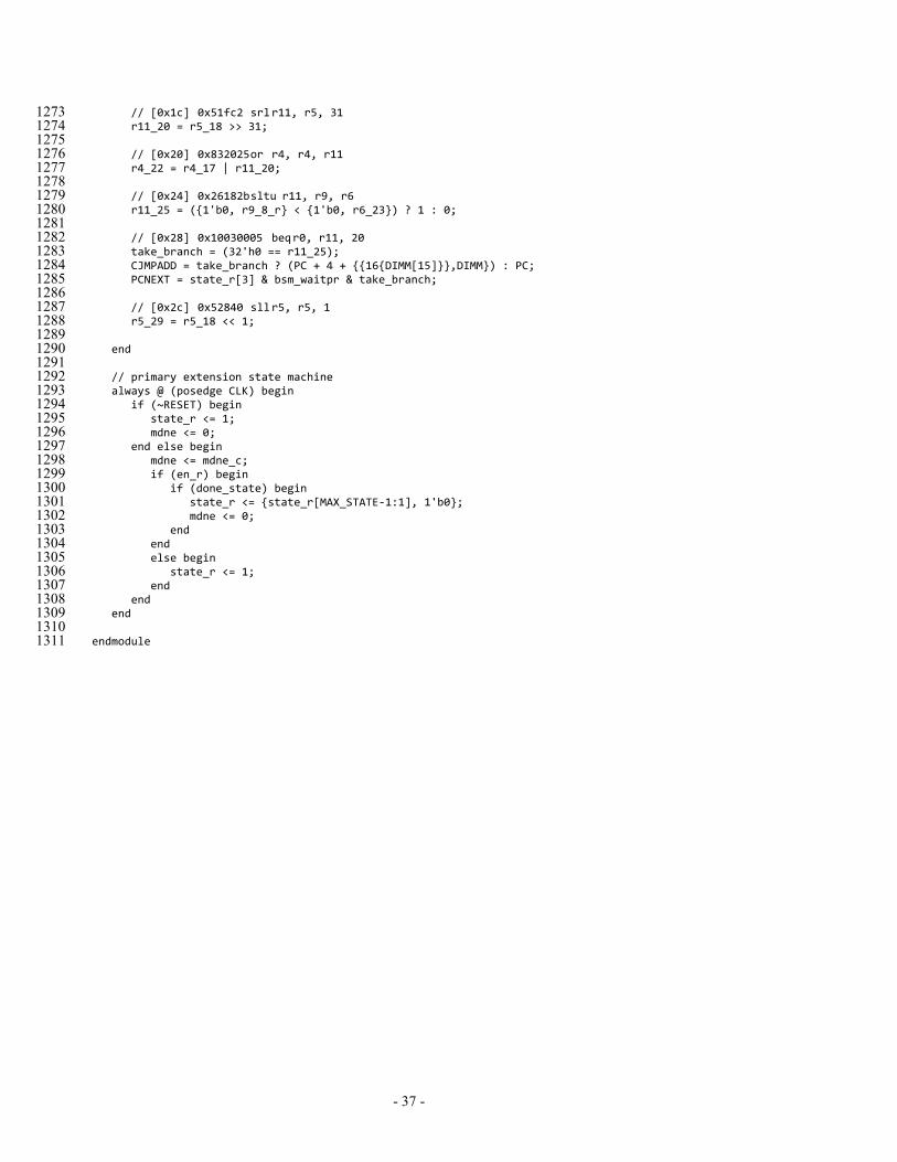
- 37 -
// [0x1c] 0x51fc2 srl r11, r5, 31 1273 r11_20 = r5_18 >> 31; 1274 1275 // [0x20] 0x832025 or r4, r4, r11 1276 r4_22 = r4_17 | r11_20; 1277 1278 // [0x24] 0x26182b sltu r11, r9, r6 1279 r11_25 = ({1'b0, r9_8_r} < {1'b0, r6_23}) ? 1 : 0; 1280 1281 // [0x28] 0x10030005 beq r0, r11, 20 1282 take_branch = (32'h0 == r11_25); 1283 CJMPADD = take_branch ? (PC + 4 + {{16{DIMM[15]}},DIMM}) : PC; 1284 PCNEXT = state_r[3] & bsm_waitpr & take_branch; 1285 1286 // [0x2c] 0x52840 sll r5, r5, 1 1287 r5_29 = r5_18 << 1; 1288 1289 end 1290 1291 // primary extension state machine 1292 always @ (posedge CLK) begin 1293 if (~RESET) begin 1294 state_r <= 1; 1295 mdne <= 0; 1296 end else begin 1297 mdne <= mdne_c; 1298 if (en_r) begin 1299 if (done_state) begin 1300 state_r <= {state_r[MAX_STATE-1:1], 1'b0}; 1301 mdne <= 0; 1302 end 1303 end 1304 else begin 1305 state_r <= 1; 1306 end 1307 end 1308 end 1309 1310 endmodule1311
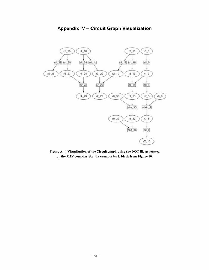
- 38 -
Appendix IV – Circuit Graph Visualization
Figure A-4: Visualization of the Circuit graph using the DOT file generated
by the M2V compiler, for the example basic block from Figure 10.