av 104 3u vpx, virtex 7 fpga - apissys x av 104 radar emitter-receiver drfm 3u vpx, virtex 7 fpga...
TRANSCRIPT
AV Series
APISSYS OpenVPX
AV Series
AV Series
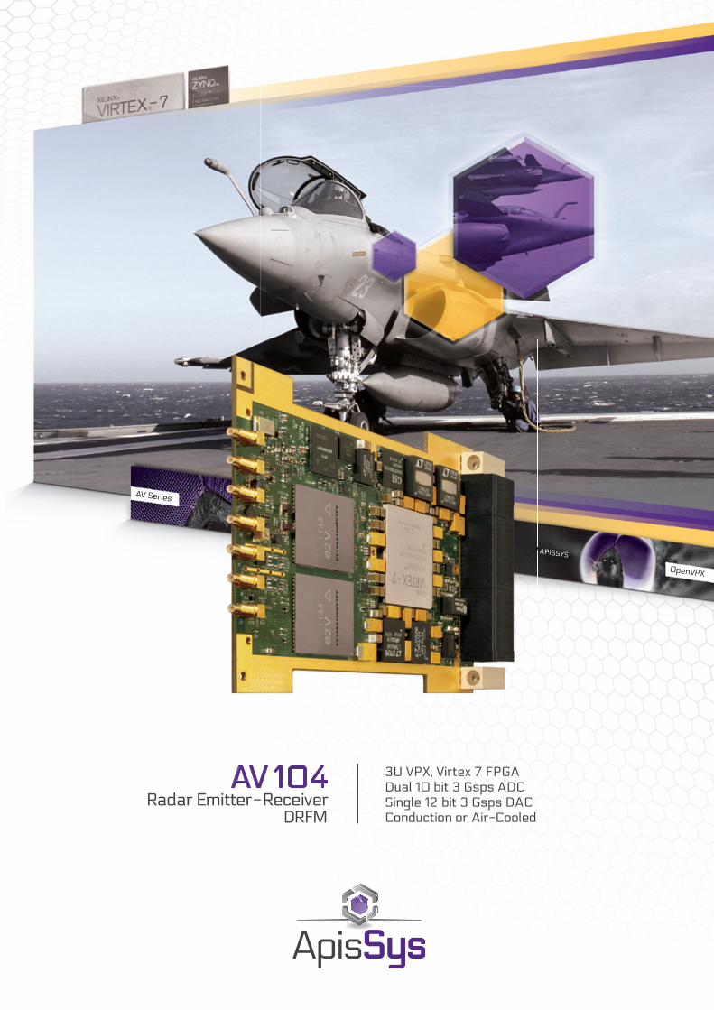
AV 104Radar Emitter-Receiver
DRFM
3U VPX, Virtex 7 FPGADual 10 bit 3 Gsps ADCSingle 12 bit 3 Gsps DACConduction or Air-Cooled
AV 104
10-bit 3 GSPS ADCThe AV104 Analog to Digital conversion is performed by two 10-bit 3 Gsps ADCs.The AV104 provides two front panel SSMC connectors for analog input.Single ended input signals are AC coupled with an input bandwidth of 5 MHz to 3 GHz or 700 MHz to 4 GHz with 2 dBm input level.
12-bit 3 GSPS DACThe AV104 Digital to Analog conversion is performed by one 12-bit 3 Gsps ADCs.The AV104 provides one front panel SSMC connector for analog output. Single ended output signal is AC coupled with an output bandwidth of 5 MHz to 3 GHz or 700 MHz to 4 GHz with -2 dBm output level.
ClockThe AV104 provides an internal ultra low jitter clock generator locked on a 100 MHz internal reference.The AV104 provides a front panel SSMC connector for a 10 to 100 MHz external refe-rence, a front panel SSMC connector for a 500 MHz to 3 GHz external clock input, and a front panel SSMC connector for an external clock output.Estimated jitter from the internal clock gene-ration (100 MHz reference and clock distribu-tion) is below 200 fs for a 3 GHz clock. Added jitter on external clock is lower than 100 fs.
Trigger and SynchronizationThe AV104 provides a front panel SSMC connector for external trigger input. The trig-ger synchronization uses the sampling clock divided by 8.
FPGAThe AV104 is fi tted with a Xilinx Virtex 7
OverviewThe AV104 is part of ApisSys’ range of High Speed data conversion and signal processing solu-tions based on the ANSI/VITA 65, OpenVPX standard.The AV104 is fully compliant with the OpenVPX standard, with default support for the MOD3-PAY-2F1F2U-16.2.1-3 and MOD3-PAY-2F1F2U-16.2.1-4 module profi les, PCIe Gen 1 or Gen 2 on Data Planes and Expansion Plane plus 1000BASE-BX on Control planes.The AV104 combines the very high processing power delivered by Xilinx® Virtex® 7 FPGA with two channels 10-bit 3 Gsps ADCs and one channel 12-bit 3 Gsps DAC, making it ideally suited for embedded signal processing applications such as Electronic Warfare, Wideband Radar Transmit-ter/Receivers or LIDAR.The AV104 provides an internal ultra low jitter clock generation and can be used with either an external clock or an external reference for higher fl exibility.The AV104 includes one Xilinx® Virtex® 7 FPGA VX330T/VX485T or VX690T for an impressive processing capability of up to more than 2 TMACs (Multiply Accumulate per second), one high speed 2M36 QDRII+ SRAM memory for data processing and a 1 Gb synchronous FLASH memory for multiple fi rmware storage.The AV104 features a 32-bit microcontroller with USB 2.0 and 10/100 Ethernet interfaces intended to be used for system monitoring and supervision.The AV104 comes with complete software drivers for Windows and Linux. An FPGA fi rmware package is provided including all cores necessary to build user FPGA applications.
Applications‧ Real time processing‧ Electronic Warfare - DRFM‧ Wideband Radar‧ LIDAR
Features‧ 2 channels 10-bit, 3 Gsps ADC‧ 1 channel 12-bit, 3 Gsps DAC‧ External clock and reference input‧ Low jitter Internal clock generation‧ External trigger input‧ User programmable Xilinx® Virtex® 7 VX330T to VX690T FPGA‧ 500 MHz 2M x 36 QDRII+ SRAM‧ 3U OpenVPX standard compliant‧ Air cooled and Conduction cooled rugged versions‧ FPGA fi rmware cores‧ Windows® and Linux® drivers
VX330T/VX485T or VX690T user program-mable FPGA. Only few resources are used to control and communicate with external hard-ware such as QDRII+ SRAM and monitoring sub-system, leaving most of the logic and block RAM and all DSP resources available for customer processing.Dedicated to signal processing, the Xilinx Vir-tex 7 VX485T FPGA includes 485,760 logics cells, 1,030 bloc RAM (36 Kbit each), 2800 DSP48E1 slices and 2 PCIe interface blocs.The most powerful version embeds a Xilinx Virtex 7 VX690T which provides 693,120 logics cells, 1,470 bloc RAM and 3,600 DSP48E1 slices for an impressive processing power of more than 2 TMACs.The FPGA is delivered in -2 speed grade.
QDRII+ SRAM MemoryThe AV104 includes one 2M36 QDRII+ SRAM memory clocked at 500 MHz for a peak data rate of 9 GB/s.
FLASH MemoryThe AV104 includes one 1 Gbit synchronous BPI FLASH used to store multiple FPGA confi guration fi les.
VPX interfaceThe AV104 features an OpenVPX VITA 65 compliant interface with support for two Fat Pipes for Data Plane, one Fat Pipe for Expan-sion Plane, two Ultra Thin Pipes for Control Plane and two User Defi ned Ultra Thin Pipes on P1. The AV104 also supports a USB2.0, a 10/100 Ethernet and 24 LVDS differential pairs on P2.The AV104 features two low phase noise clock generators able to synthesize clock re-ferences for the FPGA GTXs from 100 MHz to 312.5 MHz, allowing support of all major pro-
tocols such as Aurora, GigE, PCIe Gen 1 and Gen 2, SATA, SRIO and XAUI 10Gbit Ethernet up to 12.5 Gbps.
MicrocontrollerThe AV104 features a 32-bit 80 MHz micro-controller used primarily for board monitoring and supervision.The microcontroller supports USB 2.0 and 10/100 Ethernet interfaces accessible on the VPX P2 user IO pins through an ApisSys AR102 Rear Transition Module or an ANSI/VITA 46.10 compliant custom RTM board.The microcontroller fi rmware includes all necessary features for board monitoring and supervision, including FPGA fi rmware down-loads through Ethernet or USB.
FirmwareThe AV104 comes with a fi rmware package which includes VHDL cores allowing control and communication with all AV104 hardware resources.A base design is provided which demons-trates the use of the AV104 and gives users a starting point for fi rmware development. The AV104 fi rmware package is supported on the Xilinx ISE® 14 design suite and later.
SoftwareThe AV104 is delivered with control software for Windows 7, and Linux.RuggedizationThe AV104 is delivered in air-cooled and conduction cooled standard or rugged ver-sions for use in severe environmental condi-tions.Standard VITA 47 supported ruggedization levels are EAC4, EAC6, ECC3 and ECC4.

AV Series
APISSYS OpenVPX
SpecificationsAnalog Input/Output‧ Coupling: AC
‧ Full power bandwidth up to 4GHz‧ Full scale : 2 dBm
‧ Connector: SSMC, 50 Ohm
Analog - Digital Conversion‧ Two channels‧ Resolution: 10 bit‧ Sampling Frequency up to 3 GHz‧ 3 Gsps, Fin = 2.6 GHz, -1dBFS:
‧ SNR: 49 dBFS‧ SFDR: 52 dBc‧ ENOB: 7.6 bits
Digital - Analog Conversion‧ One channel‧ Resolution: 12 bit‧ Sampling Frequency up to 3 GHz‧ 3 Gsps, Fout = 2.6 GHz, -1dBFS:
‧ Noise density: < -150 dBm/Hz‧ SFDR 2nd Nyquist: 50 dBc
Clock‧ Internal: 500 MHz to 3 GHz low jitter clock, Internal jitter: < 200 fs‧ External Input Clock:
‧ frequency: 500 MHz to 3 GHz‧ Connector: SSMC, 50 Ohm
‧ External Output Clock:‧ frequency: sampling clock‧ Connector: SSMC, 50 Ohm
‧ External reference:‧ frequency: 10 MHz to 100 MHz‧ Connector: SSMC, 50 Ohm
Trigger‧ External: 0 to 2Vp,
‧ Connector: SSMC
FPGA‧ FPGA: Xilinx Virtex 7
‧ XC7VX330T-2FFG1157 or‧ XC7VX485T-2FFG1157 or‧ XC7VX690T-2FFG1157
Memory‧ 1 bank 2M x 36-bit QDRII+ SRAM, 500 MHz clock‧ One 1 Gbit NOR FLASH memory
VPX interface‧ P1:
‧ Data plane: two fat pipes‧ Expansion plane: one fat pipe‧ Control plane: 2 ultra-thin pipes‧ 2 user-defi ned ultra-thin pipes
‧ P2:‧ USB2.0 and 10/100 Ethernet‧ 24 LVDS differential pairs
Software support‧ Software Drivers:
‧ Windows 7‧ Linux
‧ Application example:‧ Windows and Linux
Firmware support‧ VHDL cores for all hardware resources‧ Base design‧ Supported by Xilinx ISE 13 and later
Ruggedization‧ As per VITA 47:
‧ Air cooled : EAC4 and EAC6‧ Conduction cooled : ECC3 and ECC4
Power‧ +12V: 5 A max (60W)‧ +5V: 7.4 A max (37W)‧ +3.3V: 0.5 A max (1.6W)‧ +3.3VAUX: 0.3 A max (1W)
Weight‧ Air cooled : 500g‧ Conduction cooled : 500g
Ordering information
Ruggedization level
Options 1
Options 2
Air StandardAir RuggedConduction StandardConduction Rugged
FPGA Virtex 7 VX330T-2FPGA Virtex 7 VX485T-2FPGA Virtex 7 VX690T-2
Input/Output bandwidth 5 MHz to 3000 MHzInput/Output bandwidth 700 MHz to 4000 MHz
Part Number
----
---
--
----
---
--
----
---
--
----
---
--
ASARCSCR
---
--
----
---
--
----
123
--
----
---
12
A V 104 - rr - a b
Copyright © 2011-2013 ApisSys SAS. All rights reserved. Z03-0040B.

AV Series OpenVPXDefense: Electronic Warfare systems, Wide band RadarMedical Imaging: Digital X-Ray image enhancementHigh Energy Physics
APISSYS
Ruggedization levels
OperatingTemperature
Non Operating Temperature
OperatingVibration(Random)
Operating Shock
OperatingRelative Humidity
OperatingAltitude
Conformal Coating
Air flow, StandardAS (VITA 47 EAC4)
0°C to +55°C (1)(8 CFM airfl ow at sea level)
-40°C to +85°C
5Hz - 100Hz +3 dB/octave100Hz-1kHz = 0.04 g2/Hz1kHz - 2kHz -6 dB/octave
20g, 11 millisecond, half-sine
0% to 95%non-condensing
@ 0 to 10,000 ftwith adequate airfl ow
No
Air flow, RuggedAR (VITA 47 EAC6)
-40 to +70ºC (1)(8 CFM airfl ow at sea level)
-50°C to +100°C
5Hz - 100Hz +3 dB/octave100Hz - 1kHz = 0.04 g2/Hz1kHz - 2kHz -6 dB/octave
20g, 11 millisecond, half-sine
0% to 95%non-condensing
@ 0 to 30,000 ftwith adequate airfl ow
Optional (default acrylic 1B31)
Conduction Standard CS (VITA 47 ECC3)
-40°C to +70°C(Card Edge)
-50°C to +100°C
5Hz - 100Hz +3 dB/octave100Hz - 1kHz = 0.1 g2/Hz1kHz - 2kHz -6 dB/octave
40g, 11 millisecond, half-sine
0% to 95%non-condensing
@ 0 to 30,000 ft
Yes (default acrylic 1B31)
Conduction RuggedCR (VITA47 ECC4)
-40°C to +85°C(Card Edge)
-55°C to +105°C
5Hz - 100Hz +3 dB/octave100Hz - 1kHz = 0.1 g2/Hz1kHz - 2kHz -6 dB/octave
40g, 11 millisecond, half-sine
0% to 95%non-condensing
@ 0 to 60,000 ft
Yes (default acrylic 1B31)
Phone: +33 4 50 36 07 58Fax: +33 4 50 36 05 29
Archamps Technopole60 rue Douglas EngelbartBâtiment ABC1 entrée AF-74160 Archamps, France
www.apissys.com
Specifi cations are subject to change without notice. All trademarks are property of their respective ownersCopyright © 2011-2013 ApisSys SAS. All rights reserved. Z03-0040B.
Desig
n By
ver
t-pom
me.
ch -
04.2
013