bimaterial mems thz detectors - sige mems thz... · introduction! • waves are used to acquire...
TRANSCRIPT

Bimaterial MEMS THz Detectors!
Dr.$Dragoslav$Grbovic$September$29,$2015$
XVII$Defense$Operational$Applications$Symposium$Instituto$Tecnológico$de$Aeronáutica,$São$José$dos$Campos$

Overview!
• Introduction!• THz Radiation!• Applications!• THz Detectors !• Bi-Material MEMS Detectors (4 Generations)!• Readout Mechanism!• Conclusions !
2

Introduction!
• Waves are used to acquire information!– Visible light to see our surroundings!– Radar to detect objects!– X-ray to see inside a body!– Sound to see underwater, inside a body!
• Usually, we need a source and a detector!– Light bulb (sun)/eye (camera)!– Radar transmitter/radar receiver!
• Different parts of the spectrum are used for different applications!
3

Introduction!
• THz imaging is used for “seeing through” objects!
4
advancedphotonix.com photonics.apl.washington.edu

THz Radiation!
5
1 mm > THz > 30 µm
• Low energy!• Non-ionizing!• Penetrates many materials!
– Textiles!– Cardboard!– Styrofoam!
• External Illumination needed!
E = hf = !ω

THz Imaging!
• Two modes!– Reflection!– Transmission!
6
Reflection
Transmission

Hosako, I. and Oda, N., “Terahertz imaging for detection and diagnostics,” SPIE News Room, 10.1117/2.1201105.003651 (2011); http://thznetwork.net/index.php/thz-images http://www.lakeshore.com/products/THz-System/Pages/technology.aspx; http://www.teraview.com/applications/medical/oral-healthcare.html; http://physicsworld.com/cws/article/news/2012/jun/12/new-tuner-could-bring-terahertz-to-the-masses
Security screening Food control
Non-destructive evaluation Medical diagnostics
Applications!

Applications!
8
Nature 417, 156 - 159 (2002)
www.homelandsecuritynewswire.com
cr4.globalspec.com
neenaravikumar.wordpress.com

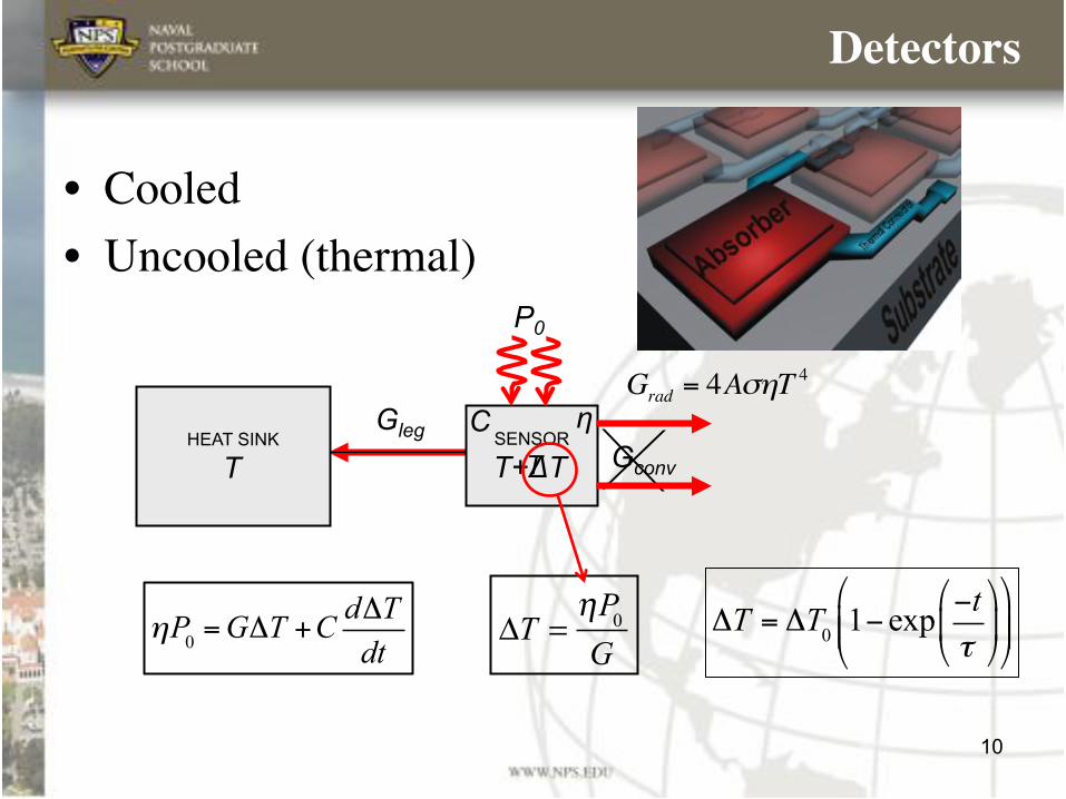
• Cooled!
Detectors!
9
f =Eg
h
Eg!
Conduction !band!
Valence !band!
hf! +
-
Detectors!
• Cooled!• Uncooled (thermal)!
10
ΔT =
ηP0
G
SENSOR
T+ΔT C η
P0
Gleg Gconv
ηP0 =GΔT +CdΔTdt
Grad = 4AσηT4
HEAT SINK
T T
ΔT = ΔT0 1− exp−tτ
#
$%
&
'(
#
$%%
&
'((

Detectors!
• Cooled!• Uncooled (thermal)!
11
SENSOR
T+ΔT C η
P0
HEAT SINK
T
Gleg
Grad <<Gleg
τ =
CG
ΔT = ΔT0 exp−tτ
$
%&'
() GΔT = −C dΔT
dt

Thermal Detectors!
• Using traditional uncooled IR cameras!• Using THz optimized microbolometers!• Using MEMS bimaterial detectors!
– With thin films!– With resonant metamaterials!
12

Using traditional IR cameras!
• Microbolometers are resistors that change temperature when they absorb appropriate radiation!
13
Behnken, B. N., Karunasiri, G., Chamberlin, D. R., Robrish, P. R., & Faist, J. (2008). Real-time imaging using a 2.8 THz quantum cascade laser and uncooled infrared microbolometer camera. Optics letters, 33(5), 440-442.

SiNx
QCL
[1] Kurashina, S. and Oda, N., "Bolometer type Terahertz wave detector." U.S. Patent No. 8,618,483. 31 Dec. 2013.(2008). [2] Alves, F., Kearney, B., Grbovic, D., Lavrik, N. V. and Karunasiri, G., "Strong terahertz absorption using SiO2/Al based metamaterial structures," App. Phys. Lett. 100(11), 111104 (2012).
[1] [2]
3.8 THz

Using traditional IR cameras!
15
http://www.ino.ca/en/products/uncooled-microbolometer-384-x-288-fpa/

MEMS!
• Micro Electro Mechanical Systems!• Rapidly developing technology!• Mainly done in silicon and silicon-based
materials!• Built upon decades of development in
microelectronics industry!• Material properties quite different at micro-
and nano-scale!
16 Yole Development

MEMS!
17
Sandia National Laboratories Sandia National Laboratories
Sensing Machines

MEMS!
18
Texas Instruments DLP Chip
Downey, R. H., L. N. Brewer, and G. Karunasiri. "Determination of mechanical properties of a MEMS directional sound sensor using a nanoindenter." Sensors and Actuators A: Physical 191 (2013): 27-33.

MEMS Everywhere!
19

MEMS Everywhere!
20

MEMS!
21 Yole Development

MEMS!
• Very versatile!• Fairly simple!• Robust!• Low cost!• Widespread!
22

THz bimaterial detectors!
• Detector deforms upon absorption of THz radiation!
23

P0 Absorber
150 µm
SENSOR
T+ΔT
MEMS bi-material sensors!

Bi-material legs
150 µm
MEMS bi-material sensors!
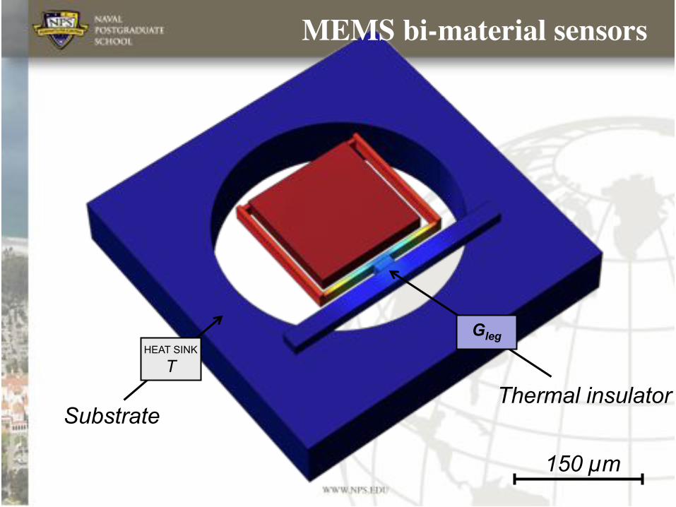
Substrate Thermal insulator
150 µm
HEAT SINK
T
Gleg
MEMS bi-material sensors!

T
T+ΔT
P0
ΔP
0 (µ
W)
Time (a. u.)
0.2!
0.4!
0.6!
0.8!
MEMS bi-material sensors!

Readout Concepts!
28
Individual Detector

Rest Position Deflected
Δθ
THz Diode Laser
ΔθΔP0
= ℜ =ηGΔθΔT
Probing the sensor angular deflection!

Readout Concepts!
30
Focal Plane Array

Probing the sensor angular deflection!
31

Probing the sensor angular deflection!
32

ΔθΔT
= 6lb t1 + t2( )t2−2 4 + 6
t1t2
+ 4t1
2
t22 +
t13
t23
E1
E2
+t2
t1
E2
E1
$
%&
'
()
−1
α1 −α2( )
Timoshenko, S., "Analysis of bi-metal thermostats," J. Opt. Soc. Amer. 11(3), 233-255 (1925).
Δzabs Δzleg
t1 t2
lb
Bi-material Leg
Δθ
Geometry Materials
Thermomechanical Sensitivity
Design Considerations!
Geometry Materials

Ther
mom
ech.
sen
sitiv
ity (d
eg
K-1
)
lb = 200 µm t2 = 1.2 µm
Alves, F., Grbovic, D., Kearney, B., Lavrik, N. V. and Karunasiri, G., "High sensitivity bi-material terahertz sensors using metamaterial structures," Opt. Exp. 21(11),13256-13271 (2013).
24.6 22.9 22.3
13.8 12.1 11.9
Bi-material Bi-material Δα
(x10-6/K) Δα
(x10-6/K)
Design Considerations!
Materials Δα =α1 −α2

Micromechanical IR Detector!
9/30/15 PH 3280 35
• Deformation magnification concept!• Using Al and SiO2!• Removing substrate underneath!!

• Temperature fluctuation noise!• Background fluctuation noise!• Thermomechanical noise!• Readout noise!
– Readout light fluctuations!– Integrated systems components vibrations!– Dark-current noise in the CCD!
PH 3280 36
€
NETDTF =4F2T 4kBBGT
τ0ηAddPdT$
% &
'
( ) λ1 −λ2
.
€
NETDBF =4F2 16kBBσ TB
5 +TD5( )
τ0 AdηdPdT%
& '
(
) * λ1 −λ2
€
NETDTM =4F2
τ0AdR ω( )dPdT$
% &
'
( ) λ1 −λ2
4kBTBQkω0
.
Noise Sources!
Grbovic, D., Lavrik, N. V., Rajic, S., & Datskos, P. G. Arrays of SiO2 substrate-free micromechanical uncooled infrared and terahertz detectors. Journal of applied physics, 104(5), 054508 (2008).

Periodic Repetition of Al elements
(~ 100 nm thick)
Al ground plane (~ 100 nm thick)
Square size: 16 – 20 µm Period: 17 – 21 µm
Alves, F., Kearney, B., Grbovic, D., Lavrik, N. V. and Karunasiri, G., "Strong terahertz absorption using SiO2/Al based metamaterial structures," App. Phys. Lett. 100(11), 111104 (2012).
Metamaterial Absorbers!

Frequency (THz)
Tran
smis
sion
THz
Metamaterial absorbers – No transmission at all!

Frequency (THz)
Ref
lect
ion
Metamaterial absorbers – No reflection at resonance!

Frequency (THz)
Abs
orpt
ion
Alves, F., Kearney, B., Grbovic, D., Lavrik, N. V. and Karunasiri, G., "Strong terahertz absorption using SiO2/Al based metamaterial structures," App. Phys. Lett. 100(11), 111104 (2012).
Metamaterial absorbers – near 100 % absorption at resonance!

d

Metal&'&Square&
Metal&–&Ground&plane&
Periodic&Boundary&
Periodic&Boundary&
Ez (x + d , y, z) = Ez (x, y, z)eidk sinθ
d
k
E i
Ez (x, y, z)
Metamaterial Unit Cell!
Arbitrary angle of incidence
Ezi

A = 1− (R + T )
d Metal&'&Square&
Metal&–&Ground&plane&
Metamaterial Unit Cell!

Port&1&
Port&2& ∇ × ∇ × E( ) − k0
2εrE = 0
∇ × ∇ × H( ) − k0
2µrH = 0
Metamaterial Unit Cell FEM!

Resistive loss
Normalized E field
Normalized H field
E field
Current circulation
Confined energy
Off resonance Resonance
Metamaterial Unit Cell FEM!

Metamaterial Fabrication!

Metamaterial Measurements!

FTIR%Measurements%
20 µm
s
Alves, F., Kearney, B., Grbovic, D., Lavrik, N. V. and Karunasiri, G., "Strong terahertz absorption using SiO2/Al based metamaterial structures," App. Phys. Lett. 100(11), 111104 (2012).
FE%Simula3ons%
Results!
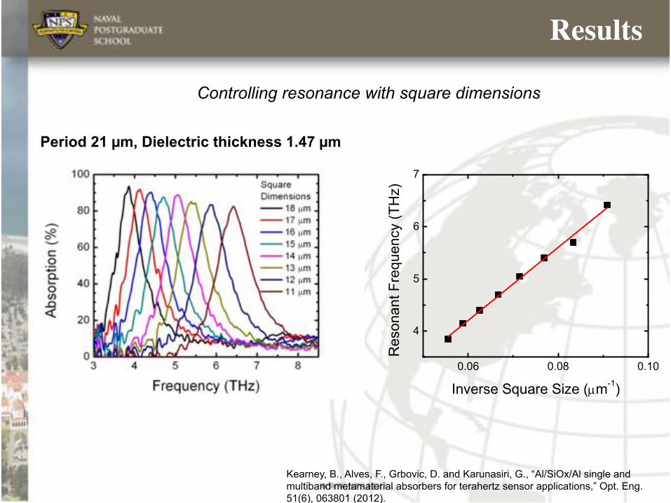
Period 21 µm, Dielectric thickness 1.47 µm
Controlling resonance with square dimensions
Kearney, B., Alves, F., Grbovic, D. and Karunasiri, G., “Al/SiOx/Al single and multiband metamaterial absorbers for terahertz sensor applications,” Opt. Eng. 51(6), 063801 (2012).
Results!
2. SINGLE BAND THz METAMATERIAL ABSORBERS Single band absorbers were fabricated with the same geometry as previously described, using SiOx as the dielectric.
Figure 4 (b) shows absorption spectrum of a metamaterial structure consists of 12 ȝm squares, 21 ȝm period, and 1.47
ȝm SiOx.
(a) (b)
Figure 2. (a) Schematics of a single band unit cell and (b) experimental vs theoretical absorption spectra for a metamaterial
with 12 ȝm squares, 21 ȝm period, and 1.47 ȝm SiOx.
When compared to similar structures that use SiO2 for the dielectric layer [11], the resonant frequency appears to be
shifted slightly as shown in Fig. 2 (b) suggesting that the differences in the material properties of SiOx and SiO2 at 3-8
THz are small, but not negligible.
The absorption spectra in Fig. 3 (a) show that as the square size is decreased, resonant frequency increases. These
structures all have a periodicity of 21 ȝm and a dielectric thickness of 1.47 ȝm. Figure 3(b) shows how the resonant
frequency changes with the square dimensions (square markers). The change in resonant frequency is clearly nonlinear
with respect to square dimensions. The solid line is a linear fit of the resonant frequency to inverse of square dimensions
since larger squares have longer wavelength (and thus lower frequency) modes [15].
(a) (b)
Figure 3. (a) Absorption measurements for varying square size, 21 ȝm period, and 1.47 ȝm SiOx and (b) resonant frequency
vs inverse of square size(solid squares). The solid line represents a linear fit.
0.06 0.08 0.10
4
5
6
7
Res
onan
t Fre
quen
cy (T
Hz)
Inverse Square Size (Pm-1)
Proc. of SPIE Vol. 8363 836309-3
Downloaded From: http://www.spiedl.org/ on 01/08/2013 Terms of Use: http://spiedl.org/terms

Controlling magnitude with dielectric thickness
Period 21 µm, Square size 12 µm
Kearney, B., Alves, F., Grbovic, D. and Karunasiri, G., “Al/SiOx/Al single and multiband metamaterial absorbers for terahertz sensor applications,” Opt. Eng. 51(6), 063801 (2012).
Results!
.
IU
a
-
-
The spectra in Fig. 4 (a) show effects of the dielectric layer thickness on absorption while all other parameters are held constant. There is a large impact on the magnitude of the absorption peak, increasing with thickness from 18% at 0.359 ȝm to 90% at 1.662 ȝm. This can be attributed to the increased contribution of evanescent waves to the Poynting flux, resulting in higher resistive losses in the metal [15]. Figure 4(b) shows the magnitude of absorption peak versus the dielectric layer thickness (solid squares), while the solid line represents the quadratic polynomial fit to the data. Additionally, it is clear that changes in the dielectric thickness also cause minor variations in the resonant frequency of the metamaterial (see Fig. 4(a)).
(a) (b)
Figure 4. (a) Measured absorption for a set of SiOx thicknesses while keeping square size to 12 ȝm and period to 21 ȝm and (b) maximum absorption amplitude vs dielectric layer thickness (fitted to quadratic polynomial).
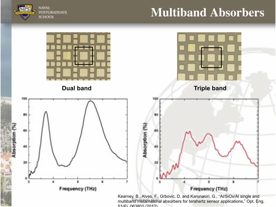
3. DUAL BAND THz METAMATERIAL ABSORBERS
The dual band design involves alternating the squares in a fashion reminiscent of a checkerboard as illustrated in Fig. 5 (a). Two different metamaterial structure were fabricated with 16 and 18 ȝm squares (2 ȝm size difference) and 13 and 17 ȝm squares (4 ȝm size difference). Additionally, the 13 and 17 ȝm single band absorbers were fabricated without their counterpart, while in the same position as the original design as shown in Fig. 5(a).
(a) (b) (c)
Figure 5 (a) Unit cell (black square outline) of the 'checkerboard' dual band metamaterial, (b) comparison of the absorption spectrum for dual band absorber with 2 ȝm square size difference, overall period of 42 ȝm and SiOx thickness 1.47 ȝm to a single band absorber with an intermediate square size and (c) measured absorption spectrum for the sample with 4 ȝm square size difference.
0.0 0.5 1.0 1.5 2.00
20
40
60
80
100
Max
Abs
orpt
ion
Ampl
itude
(%)
Dielectric Thickness (Pm)
Proc. of SPIE Vol. 8363 836309-4
Downloaded From: http://www.spiedl.org/ on 01/08/2013 Terms of Use: http://spiedl.org/terms
Kearney, B., Alves, F., Grbovic, D. and Karunasiri, G., “Al/SiOx/Al single and multiband metamaterial absorbers for terahertz sensor applications,” Opt. Eng. 51(6), 063801 (2012).
Triple band Dual band
Multiband Absorbers!

Results!
52
!

Detector Design!
• Incorporate the metamaterials into the bimaterial detectors!
• Use finite element modeling to test behavior of various designs before microfabrication!
53

Alves, F., Grbovic, D. and Karunasiri, G., "Investigation of MEMS bi-material sensors with metamaterial absorbers for THz imaging ,” Opt. Eng. (2014).
Modeling entire sensor!

ΔθΔP0
= ℜ =ηGΔθΔT
299
T (K)
298
297
296
295
294
293
Time domain FE simulations
τ = C
Gtot
B
A
B
C
QCL
τ = 0.4 s
ℜ = 1.0 deg/µW
A τ = 0.65 s
ℜ = 1.4 deg/µW
C τ = 0.1 s
ℜ = 0.25 deg/µW
Optimizing Thermal Conductance!

Substrate
Detector Microfabrication!
Al evaporation – Ground plane
Al etch – Ground plane
SiOx PECVD deposition - Structure
1
2
3
4

Al evaporation – Resonator array
Detector Microfabrication!
Al etch – Resonator array
Al evaporation – Bi-material legs
Al Liftoff – Bi-material leg
5
6
7
8

SiOx etch - Structure
Detector Microfabrication!
Top side protection
Bottom side 9
10
11
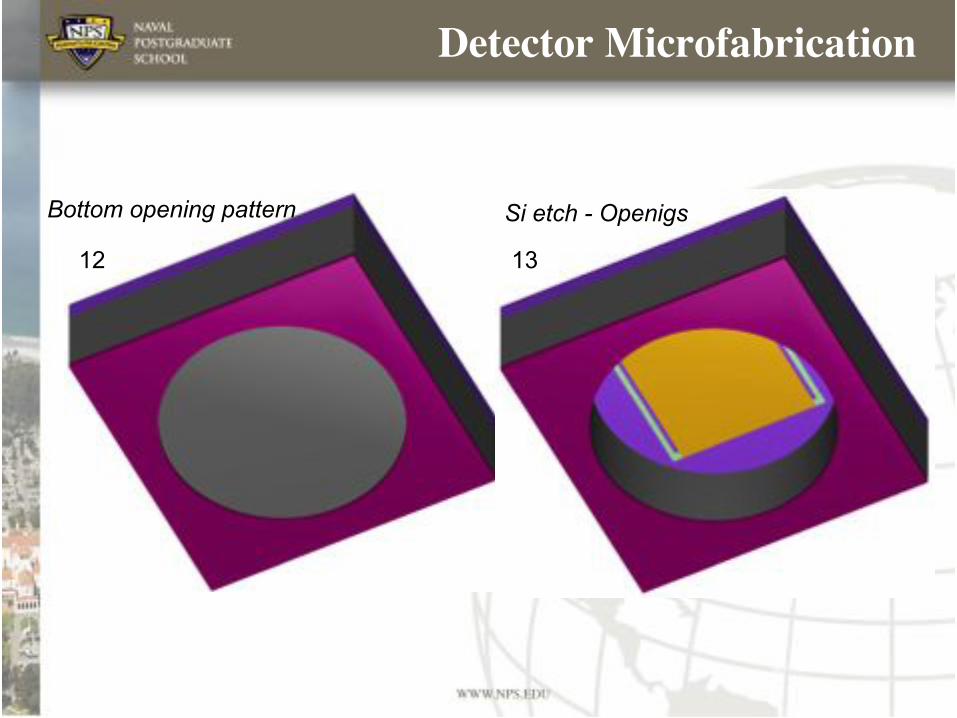
Bottom opening pattern
Detector Microfabrication!
Si etch - Openigs
12 13

Sensor release
Detector Microfabrication!
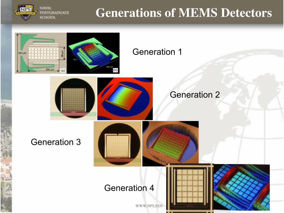
Generations of MEMS Detectors!
61
!
Fig. 8. Fabricated THz bi-material sensors. (a) 3D optical profile of sensor A (the aspect ratio is preserved). (b) Micrograph of an array of sensor A. (c) 2D profile taken along the bi-material legs direction (y-profile) with the processing direction (z-profile) scale exaggerated to show the residual deflection of the legs (red line) and absorber (blue line). (c) Micrographs showing the top view of sensors A, B and C.
Table 2. THz bi-material sensor analytical numerical and experimental parameters.
Sensor Sensor A Sensor B Sensor C
Property Anal. FE Exp. Anal. FE Exp. Anal. FE Exp. Absorptance
Ș – 0.96 0.95 – 0.96 0.95 – 0.96 0.95
Thermal Conductance
G ( × 10−7 W K−1) 1.6 1.7 – 2.2 2.1 – 9.3 8.5 –
Thermal Capacitance C ( × 10−8 J K−1)
11.1 12 – 10.7 12.5 – 9.8 11.9 –
Time constant IJ (s) 0.68 0.7 0.8 0.47 0.6 0.5 0.1 0.14 0.3
Thermomechanical Sensitivity
dș/dT (deg K−1) 0.15 0.19 0.2 0.15 0.2 0.2 0.15 0.2 0.2
Responsivity dș/dP ( × 106 deg
W−1) 0.95 1.1 1.2 0.65 0.9 0.8 0.15 0.25 0.2
Noise Equivalent Power
(due to incident power)
NEP ( × 10−9 W)
0.005 – 8.6 0.006 – 13 0.014 – 45
#181610 - $15.00 USD Received 12 Dec 2012; revised 25 Jan 2013; accepted 24 Feb 2013; published 23 May 2013(C) 2013 OSA 3 June 2013 | Vol. 21, No. 11 | DOI:10.1364/OE.21.013256 | OPTICS EXPRESS 13267
(a)
Verticaldisp. (pm)
12
6
0
-6
-12
(b) (c)
1.0
0.8
8m 0.6El-ÿ 0.4
0.2
0.0
3.8 THz
3 0 3.5 4.0 4.5
Frequency (THz)
(a)
50
5
2.0
1.5
1.0
0.5
0.0
Sensor Response- Linear Fit
- 0.2 deg/K
302 304 306 308 310Temperature (K)
(b)
312 314
Figure 5. Comparison between simulated and fabricated sensors. (a) COMSOL simulation of the released sensor including
residual stress. (b) Optical profile of the fabricated sensor (realistic view). The surface color in both simulated (a) and
measured (b) indicates the vertical displacement, according to the color bar. (c) Micrograph of the fabricated sensor.
In addition to the sensor, the wafer contains a 10x10 mm2 area filled with the same metamaterial structure used in the
sensor to allow absorption measurements. Reflectance measurements were performed using a Thermo-Nicolet Nexus
870 Fourier Transform Infrared Spectrometer (FTIR) with a globar source fitted with a PIKE Technologies MappIR
accessory. An aluminum-coated section of the wafer was used to establish the background for the reflectance
measurements. Absorptance was then obtained by 1-R, and is shown in Fig. 6(a). Notice that the good match between
the QCL source emission and the peak absorption of the metamaterial absorber incorporated in the sensor. The thermal
response of the sensor (dT/dT) was measured by attaching the substrate to a flat resistive heating element and sweeping
the temperature from 303 to 313 K. The reflection of a laser diode beam from the backside of the sensor’s ground plane
was projected on a screen to determine the angular deflection of the sensor. Figure 6(b) shows the measured angular
deflection as a function of temperatures. The solid line is a linear fit, showing that the sensor response in this
temperature range is linear and approximately 0.2 deg/K. The measured value is also included in Fig 2(b) and found to
be close to that of the estimated using Eq. 2.
Figure 6. Measured parameters of the sensor. (a) Metamaterial absorption. The dashed line indicates the frequency of the
QCL illuminator. (b) Measured angular deflection due to temperature change. The solid line is a linear fit with slope ~ 0.2
deg/K.
Next, the sensor was placed in a vacuum chamber and operated at a pressure of approximately 0.03 mTorr. The beam
from a 3.8 THz QCL, was directed toward the sensor and its deflection was measured using the same procedure
described earlier for a range of QCL output power. The absolute power that reaches the sensors is estimated substituting
the angular deflection, the calculated thermal conductance and measured absorptance in Eq. 1. Figure 7(a) show the
Proc. of SPIE Vol. 8624 862411-6
Downloaded From: http://proceedings.spiedigitallibrary.org/ on 05/02/2013 Terms of Use: http://spiedl.org/terms
Generation 1
Generation 2
Generation 4
Generation 3

Generation 1!
• Δθ/ΔT = 0.42 deg/K!• R = 0.1 deg/µW!• τ = 14 ms!• NEP = 1.75 nW!
62
!
with periodicity of 20 μm separated from an Al groundplane by a SiO2 layer. The Al and SiO2 layers are about100 nm and 1.2 μm thick, respectively. The absorbingarea of the pixel is 88 × 200 μm2 and contains 40 Alsquares to form the metamaterial structure.The THz detectors were fabricated using standard mi-
cromachining technology. First, a 100 nm thick alumi-num (Al) film is deposited on a 300 μm thick silicon(Si) substrate. Then, the Al layer is patterned usingphotolithography and sputter-etched to form the absor-ber array and the first pair of aluminized legs (closestto the absorber). Next, a 1.2 μm thick silicon dioxide(SiO2) layer is deposited using plasma enhanced chemi-cal vapor deposition (PECVD) at 300 °C, followed by an-other 100 nm thick Al film.The second metal layer is then patterned using photo-
lithography and wet etched to define the absorberground plane (which also acts as a reflector for the op-tical readout of deformation due to the heat generatedfrom THz absorption) and the second pair of aluminizedlegs with Al on the opposite side. The sensor structure isthen patterned by reactive ion etching the SiO2 layer todefine the pixel as shown in Fig. 1(a). The two outer armsof the folded leg on each side attached to the substrate(in green) do not have Al and provide thermal insulationto the pixel. Finally, the structures were released throughbackside trenching using the Bosch etch process. Theprofile of a released pixel measured using optical profi-lometry is shown in Fig. 1(b), where the deformation ofthe pixel membrane is due to residual stress after fabri-cation. Such a deformation does not affect the sensitivityof the sensor and can be minimized by further refiningthe fabrication process.The absorption properties of the metamaterial struc-
ture were simulated using COMSOL multiphysics soft-ware, a three-dimensional finite element modelingprogram, and are shown by the dashed line in Fig. 2.The index of refraction of SiO2 at THz frequencies wastaken from [15] as 2.0! 0.025i and a conductivity of 1 ×10⁷ S∕m was used for Al. The spectral characteristics ofthe fabricated metamaterial were measured using a Four-ier transform infrared spectrometer (FTIR) extended to
THz range and appropriate accessories. The measuredabsorption is shown in Fig. 2 (dotted line) along withthe QCL source emission characteristics (solid line).Note that the laser frequency matches well with the max-imum absorption of the metamaterial structure. Goodagreement between measured and simulated absorptionspectra indicates that the finite element modeling ap-proach employed can be used to design metamaterialabsorbers with the desired spectral characteristics.
The thermal response of the sensor was obtained byattaching it to a heating element and using a linear photo-diode array (linear positioning system) to measure thedeflection of a HeNe laser beam reflected by the pixel.Figure 3 shows the measured angular displacement ofthe pixel membrane as a function of temperature.
The angular displacement is nearly linear with a neg-ligibly small hysteresis. The measured thermal responseis comparable to that in [4] for similar structures (withouta metamaterial absorber) employed as an infrared sen-sor. The angular displacement can be further increasedby optimizing the aluminum and SiO2 layers thicknesseson the legs.
An important parameter for imaging applications is thesensor’s operation speed. This parameter was measuredusing the same procedure used in the thermal response,except that the sensor was placed in a vacuum chamberto reduce convection heat loss. The THz beam from theQCL was directed to the detector using a combination oftwo off-axis parabolic mirrors. The inset in Fig. 4 showsthe temporal response of the sensor when the QCL powersupply is gated using a square pulse generator operatingat 1 Hz. The measurement clearly shows that the absorp-tion of THz from the laser deflects the pixel membrane.The sensor’s operation speed was also measured bychanging the gating rate of the power supply as shownin Fig. 4, which indicates that the sensitivity of the pixeldiminishes beyond about 100 Hz. The 3 dB cutoff fre-quency was found to be around 11 Hz, giving a time con-stant of about 14 ms, which is in the same ballpark asmicrobolometer infrared detectors [16].
The speed of the sensor is primarily limited by the ther-mal time constant (τ), which is given by the ratio betweenthe heat capacitance (C) and the thermal conductance(G) [16]. The thermal capacitance of the sensor was
Fig. 2. (Color online) Measured (dotted curve) and simulated(dashed curve) absorption spectra of the metamaterial struc-ture. Note that the peak absorption matches well with the mea-sured QCL emission frequency (solid curve).
Fig. 3. (Color online) Angular deflection of the pixel mem-brane as a function of temperature by heating it under ambientconditions.
June 1, 2012 / Vol. 37, No. 11 / OPTICS LETTERS 1887
F Alves, D Grbovic, B Kearney, G Karunasiri, “Microelectromechanical systems bimaterial terahertz sensor with integrated metamaterial absorber” Optics letters 37 (11), 1886-1888

Generation 1!
63
Video of laser beam moving with the moving sensor

THz bimaterial detectors!
64
• Various designs tested at NPS!• Bimaterial devices exhibit stress!
!
!
Optical Engineering 53 (9), 097103-097103 (2014)
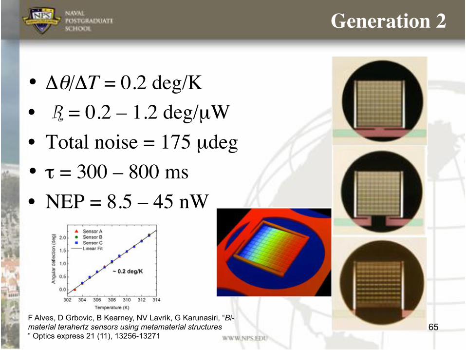
Generation 2!
65
Fig. 8. Fabricated THz bi-material sensors. (a) 3D optical profile of sensor A (the aspect ratio is preserved). (b) Micrograph of an array of sensor A. (c) 2D profile taken along the bi-material legs direction (y-profile) with the processing direction (z-profile) scale exaggerated to show the residual deflection of the legs (red line) and absorber (blue line). (c) Micrographs showing the top view of sensors A, B and C.
Table 2. THz bi-material sensor analytical numerical and experimental parameters.
Sensor Sensor A Sensor B Sensor C
Property Anal. FE Exp. Anal. FE Exp. Anal. FE Exp. Absorptance
Ș – 0.96 0.95 – 0.96 0.95 – 0.96 0.95
Thermal Conductance
G ( × 10−7 W K−1) 1.6 1.7 – 2.2 2.1 – 9.3 8.5 –
Thermal Capacitance C ( × 10−8 J K−1)
11.1 12 – 10.7 12.5 – 9.8 11.9 –
Time constant IJ (s) 0.68 0.7 0.8 0.47 0.6 0.5 0.1 0.14 0.3
Thermomechanical Sensitivity
dș/dT (deg K−1) 0.15 0.19 0.2 0.15 0.2 0.2 0.15 0.2 0.2
Responsivity dș/dP ( × 106 deg
W−1) 0.95 1.1 1.2 0.65 0.9 0.8 0.15 0.25 0.2
Noise Equivalent Power
(due to incident power)
NEP ( × 10−9 W)
0.005 – 8.6 0.006 – 13 0.014 – 45
#181610 - $15.00 USD Received 12 Dec 2012; revised 25 Jan 2013; accepted 24 Feb 2013; published 23 May 2013(C) 2013 OSA 3 June 2013 | Vol. 21, No. 11 | DOI:10.1364/OE.21.013256 | OPTICS EXPRESS 13267
• Δθ/ΔT = 0.2 deg/K!• R = 0.2 – 1.2 deg/µW!• Total noise = 175 µdeg!• τ = 300 – 800 ms!• NEP = 8.5 – 45 nW!
Fig. 8. Fabricated THz bi-material sensors. (a) 3D optical profile of sensor A (the aspect ratio is preserved). (b) Micrograph of an array of sensor A. (c) 2D profile taken along the bi-material legs direction (y-profile) with the processing direction (z-profile) scale exaggerated to show the residual deflection of the legs (red line) and absorber (blue line). (c) Micrographs showing the top view of sensors A, B and C.
Table 2. THz bi-material sensor analytical numerical and experimental parameters.
Sensor Sensor A Sensor B Sensor C
Property Anal. FE Exp. Anal. FE Exp. Anal. FE Exp. Absorptance
Ș – 0.96 0.95 – 0.96 0.95 – 0.96 0.95
Thermal Conductance
G ( × 10−7 W K−1) 1.6 1.7 – 2.2 2.1 – 9.3 8.5 –
Thermal Capacitance C ( × 10−8 J K−1)
11.1 12 – 10.7 12.5 – 9.8 11.9 –
Time constant IJ (s) 0.68 0.7 0.8 0.47 0.6 0.5 0.1 0.14 0.3
Thermomechanical Sensitivity
dș/dT (deg K−1) 0.15 0.19 0.2 0.15 0.2 0.2 0.15 0.2 0.2
Responsivity dș/dP ( × 106 deg
W−1) 0.95 1.1 1.2 0.65 0.9 0.8 0.15 0.25 0.2
Noise Equivalent Power
(due to incident power)
NEP ( × 10−9 W)
0.005 – 8.6 0.006 – 13 0.014 – 45
#181610 - $15.00 USD Received 12 Dec 2012; revised 25 Jan 2013; accepted 24 Feb 2013; published 23 May 2013(C) 2013 OSA 3 June 2013 | Vol. 21, No. 11 | DOI:10.1364/OE.21.013256 | OPTICS EXPRESS 13267
F Alves, D Grbovic, B Kearney, NV Lavrik, G Karunasiri, “Bi-material terahertz sensors using metamaterial structures ” Optics express 21 (11), 13256-13271
The absorptance of the metamaterial film was measured as described in section 4 and compared with the QCL emission characteristics as shown in Fig. 9(a). A good match between the absorptance peak position of the metamaterial and the 3.8 THz QCL emission frequency was achieved with nearly 95% absorptance. This assured that the sensors absorbed our QCL emission with high efficiency.
Fig. 9. (a) Measurement of the absorptance spectra of the THz sensors metamaterial structure (blue line) compared with the QCL normalized emission (read line). (b) Measured angular deflection (markers) upon temperature chance. Notice that the effect is linear and almost indistinguishable among the sensors, resulting in approximately 0.2 deg/K thermomechanical sensitivity.
Next, the thermal response of the sensor (dș/dT) was measured. The temperature gradient in the bi-material section of the leg was estimated to be less than 5% of that between the central absorbing element and the substrate. Thus, the bi-material section of the leg can be treated as thermally shorted allowing the measurement of the thermal response by uniformly heating the sensor. The measurement was performed by attaching the sensor to a flat resistive heating element and sweeping the temperature from 303 to 313 K. The reflection of a laser diode beam from the backside of the sensor’s ground plane was projected on a screen and the angular deflection of the sensor was determined. Angular deflections from the three sensors are shown in Fig. 9(b) with different markers. The deflections are almost indistinguishable because the detectors have the same bi-material leg dimensions. The solid line is a linear fit, showing that the response in this temperature range is linear and approximately 0.2 deg/K, which is slightly higher than the estimated values (see Table 2 and Fig. 2). Figure 2 shows that the thermal response of the sensors can be further increased by, for example, decreasing the SiOx thickness or increasing the Al thickness on the legs. Test structures fabricated in parallel with these sensors showed that increasing the Al thickness on the legs also increases the residual stress. Decreasing the dielectric thickness has a similar effect in addition to reducing absorber efficiency [27]. Further tuning of the fabrication process is necessary to reduce the residual stress on the bi-material legs to decrease the initial bending as depicted in Fig. 8(a).
Subsequently, the sensors were placed in a vacuum chamber and operated at a pressure of approximately 0.03 mTorr to minimize the heat loss by convection [29]. The QCL was kept inside a cryostat and operated at around 15 K. The divergent THz beam passed through the cryostat Tsurupica window and the radiation was focused by a 40 mm polyethylene lens onto the sensors. Both Tsurupica and polyethylene exhibit reasonable transmission (~65%) in the THz range. The QCL was operated in pulsed mode with the pulse width fixed at 5 ȝs and a variable pulse rate to control the output power. The deflection of the sensor was measured using the same procedure described earlier for a set of QCL pulse rates ranging from nearly zero to 5 kHz. The absolute power that reaches the sensors (incident power) is estimated
#181610 - $15.00 USD Received 12 Dec 2012; revised 25 Jan 2013; accepted 24 Feb 2013; published 23 May 2013(C) 2013 OSA 3 June 2013 | Vol. 21, No. 11 | DOI:10.1364/OE.21.013256 | OPTICS EXPRESS 13268

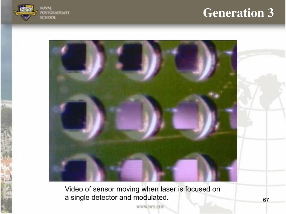
Generation 3!
66
(a)
Verticaldisp. (pm)
12
6
0
-6
-12
(b) (c)
1.0
0.8
8m 0.6El-ÿ 0.4
0.2
0.0
3.8 THz
3 0 3.5 4.0 4.5
Frequency (THz)
(a)
50
5
2.0
1.5
1.0
0.5
0.0
Sensor Response- Linear Fit
- 0.2 deg/K
302 304 306 308 310Temperature (K)
(b)
312 314
Figure 5. Comparison between simulated and fabricated sensors. (a) COMSOL simulation of the released sensor including
residual stress. (b) Optical profile of the fabricated sensor (realistic view). The surface color in both simulated (a) and
measured (b) indicates the vertical displacement, according to the color bar. (c) Micrograph of the fabricated sensor.
In addition to the sensor, the wafer contains a 10x10 mm2 area filled with the same metamaterial structure used in the
sensor to allow absorption measurements. Reflectance measurements were performed using a Thermo-Nicolet Nexus
870 Fourier Transform Infrared Spectrometer (FTIR) with a globar source fitted with a PIKE Technologies MappIR
accessory. An aluminum-coated section of the wafer was used to establish the background for the reflectance
measurements. Absorptance was then obtained by 1-R, and is shown in Fig. 6(a). Notice that the good match between
the QCL source emission and the peak absorption of the metamaterial absorber incorporated in the sensor. The thermal
response of the sensor (dT/dT) was measured by attaching the substrate to a flat resistive heating element and sweeping
the temperature from 303 to 313 K. The reflection of a laser diode beam from the backside of the sensor’s ground plane
was projected on a screen to determine the angular deflection of the sensor. Figure 6(b) shows the measured angular
deflection as a function of temperatures. The solid line is a linear fit, showing that the sensor response in this
temperature range is linear and approximately 0.2 deg/K. The measured value is also included in Fig 2(b) and found to
be close to that of the estimated using Eq. 2.
Figure 6. Measured parameters of the sensor. (a) Metamaterial absorption. The dashed line indicates the frequency of the
QCL illuminator. (b) Measured angular deflection due to temperature change. The solid line is a linear fit with slope ~ 0.2
deg/K.
Next, the sensor was placed in a vacuum chamber and operated at a pressure of approximately 0.03 mTorr. The beam
from a 3.8 THz QCL, was directed toward the sensor and its deflection was measured using the same procedure
described earlier for a range of QCL output power. The absolute power that reaches the sensors is estimated substituting
the angular deflection, the calculated thermal conductance and measured absorptance in Eq. 1. Figure 7(a) show the
Proc. of SPIE Vol. 8624 862411-6
Downloaded From: http://proceedings.spiedigitallibrary.org/ on 05/02/2013 Terms of Use: http://spiedl.org/terms
• Δθ/ΔT = 0.2 deg/K!• R = 1.2 deg/µW!• τ = 300 !• NEP = 9 nW!
F Alves, D Grbovic, B Kearney, NV Lavrik, G Karunasiri, “Bi-material terahertz sensors using metamaterial structures”, Optics express 21 (11), 13256-13271
2.0
1.5
1.0
0.5
0.0
0.0 0.5 1.0 1.5 2.0 2.5Incident power (µW)
(a)
1.0
0)
0.8
0.6
Ñ 0.4E
0.2Z
1.2E 0.9
0.50.30.0-0.3-0.5
00
-Sens rResModulation
ones(1 Hs)-
V
CCL
V V0.5 1.0 1.5 2.0 25
Time (a)
i=0.3s
0.1 1 10
Frequency (Hz)(b)
100
measured angular deflection of the detector as a function of incident power. A position-sensing detector was added to the setup to allow the measurement of the minimum detectable incident power or noise equivalent power (NEP) and time domain measurements. The inset in Fig. 7(a) shows PSD output translated in incident power when the QCL is gated at 200 mHz. It is worth to notice that those measurements included the contribution of the readout noise and QCL fluctuations which is significantly grater than the intrinsic noise of the sensor24. The measurement of the minimum detectable power (due to noise from sensor and readout system) was approximately 9 nW, which translates into minimum detectable temperature of about 50 mK and it is similar to that of bi-material sensors operating in the IR range7, 25. The time constant of the sensor was determined by sweeping the QCL gating frequency from 50 mHz to 30 Hz and recording the PSD peak to peak voltage. The normalized frequency response is shown in Fig. 7(b). The time constant was retrieved from Fig. 7(b) by taking the inverse of the 3 dB frequency and included in Table 3 (check). The inset of Fig. 7(b) shows the sensor response in the time domain when the QCL source is modulated at 1 Hz.
Figure 7. Responsivity and speed of operation measurements. (a) Measured angular deflection per varying incident power. The inset shows the minimum detectable power measured for the QCL gated at 200 mHz. (b) Normalized frequency response. The time constant is ~0.3 s. The inset shows the time response of the sensor when the QCL is gated at 1 Hz.
Table 3. THz bi-material sensor FE and experimental parameters.
Parameter Absorptance
K
Thermal Conductance G (u10-7 W K-1)
Thermal Capacitance C (u10-7 J K-1)
Time constant
W (s)
Thermomechanical Sensitivity
dT/dT (deg K-1)
Responsivity
dT/dP (u106 deg W-1)
Noise Equivalent Power
NEP (u10-9 W)
COMSOL 0.95 1.7 0.85 0.45 0.19 1.1 ---
Measurement 0.97 -- -- 0.3 0.2 1.2 9
In general, the measured parameters agree well with the FE estimations. The sensor is apparently slow for real time imaging, however, since high sensitivity was achieved, pixel size can be reduced to increase the speed of operation. A tradeoff between speed and sensitivity has to be made according to specific applications.
4. CONCLUSION In summary, we have demonstrated a metamaterial-based bi-material MEMS sensor operating in the THz range. Sensor materials and configurations were chosen in order to maximize responsivity. The favorable combination of thermal, mechanical and optical properties of the MEMS fabrication-friendly materials SiOx and Al were advantageous for structural, bi-material and metamaterial effects. Finite element models were used to predict the performance of the sensors. A highly efficient metamaterial structure was developed to provide near 100% absorption at 3.8 THz, while simultaneously serving as a structural layer and providing access for external optical readout. The fabricated sensor
Proc. of SPIE Vol. 8624 862411-7
Downloaded From: http://proceedings.spiedigitallibrary.org/ on 05/02/2013 Terms of Use: http://spiedl.org/terms
Generation 3!
67
Video of sensor moving when laser is focused on a single detector and modulated.

• Δθ/ΔT – not measurable with our method!• R - TBA!• τ – TBA !
Generation 4!
68
F Alves, D Grbovic, J Arruda, R Santos, G Karunasiri, “Improving sensitivity and defying residual stress in MEMS bi-material terahertz sensors with metamaterial structures and self-leveling configuration”, Advanced Electromagnetic Materials in Microwaves and Optics – Metamaterials, IEEE (2014)
zxy

Addressing Noise!
69
Self-leveling configuration
When the environment temperature (T) fluctuates
T+ΔT
T

Addressing Noise!
70
Self-leveling configuration Δ
P0
(µW
)
Time (a. u.)
0.2!
0.4!
0.6!
0.8!

Good reflector for the optical readout
Residual stress compensation
(“sandwich structure”)
Alves, F., Grbovic, D., Kearney, B. and Karunasiri, G., "Microelectromechanical systems bimaterial terahertz sensor with integrated metamaterial absorber," Opt. Lett. 37(11), 1886-1888 (2012).
The same materials used for the bi-material legs – easier fabrication
Addressing Stress!

Addressing Stress!
72
Metamaterial Metallic thin film
Measured 3D profile Measured 3D profile
Alves, F., Grbovic, D., Arruda, J., Santos, R. and Karunasiri, G., "Improving sensitivity and defying residual stress in MEMS bi-material terahertz sensors with metamaterial structures and self-leveling configuration ," To appear in Proc. of IEEE Metamaterials 2014.
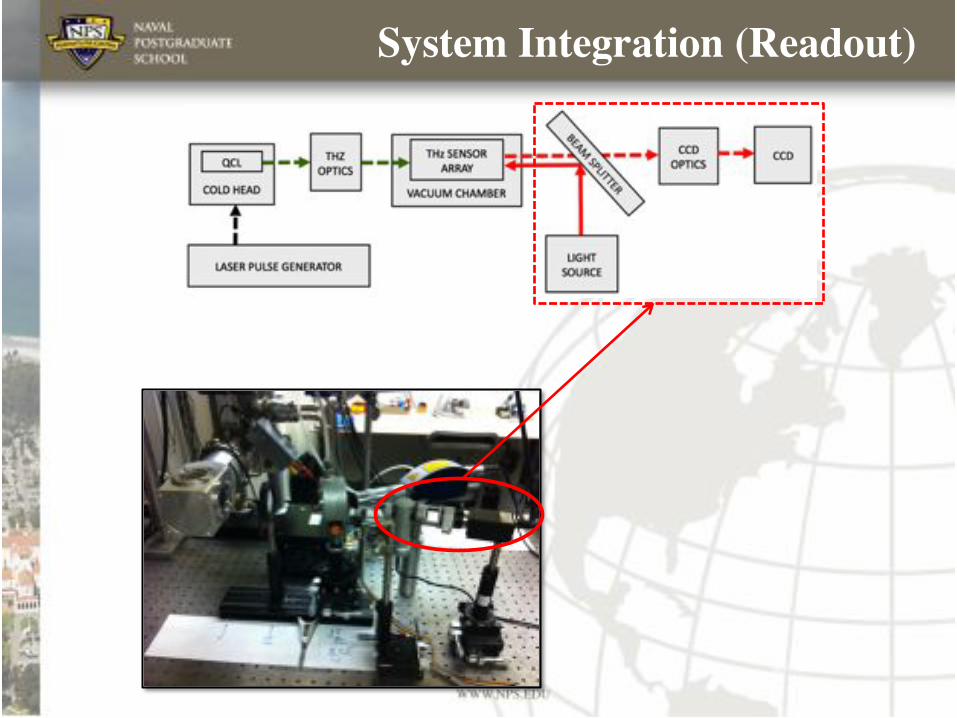
System Integration (Readout)!

THz&sensor&Array&(8'10)&
System Integration (Readout)!

Optical readout!
• THz illumination on one side!• LED illumination on the other side!• Regular CCD images the LED-illuminated
FPA to reconstruct the image!
75
!

Conclusions!
• MEMS Bimaterial detectors can provide simpler, more robust THz imaging systems!
• Some of the issues present in MEMS devices do not necessarily have to work against their use as THz detectors!
• Balance between speed and sensitivity is intrinsic to the operation and needs to be taken into account.!
76

Muito Obrigado!!
Perguntas?!
77