bjt transistor modeling - hacettepe universityusezen/ele230/bjt_ssac-2sp.pdf5 hybrid equivalent...
TRANSCRIPT

Contents
BJT Small-Signal Analysis
Purpose of SSAC AnalysisBJT SSAC Analysis Steps
BJT Small-Signal ModelsHybrid Equivalent Model
Common-Emitter Fixed-Bias CongurationInput Resistance
Voltage Gain
Output Resistance
Phase Relationship
Common-Emitter Voltage-Divider Bias CongurationInput Resistance
Voltage Gain
Output Resistance
Phase Relationship
Common-Emitter Unbypassed-Emitter Bias CongurationInput Resistance
Voltage Gain
Output Resistance
Phase Relationship
Emitter-Follower CongurationInput Resistance
Voltage Gain
Output Resistance
Phase Relationship
Common-Emitter Collector Feedback CongurationInput Resistance
Voltage Gain
Output Resistance
Phase Relationship
Common-Base CongurationInput Resistance
Voltage Gain
Output Resistance
Phase Relationship
Dr. U. Sezen & Dr. D. Gökcen (Hacettepe Uni.) ELE230 Electronics I 21-Apr-2018 1 / 59
BJT Small-Signal Analysis Purpose of SSAC Analysis
Purpose of SSAC Analysis
The purpose of small-signal AC (SSAC) analysis to determine the three parameters of anamplier input resistance, output resistance and gain. In this course, we are mostlyinterested in the two-port voltage-gain amplier model shown below.
Input resistance Ri is dened by the no-load input voltage of the amplier divided by theno-load input current to the amplier, i.e.,
Ri =vi
ii
∣∣∣∣RL=∞
NOTE: Input resistance cannot include the source resistance Rs.
Dr. U. Sezen & Dr. D. Gökcen (Hacettepe Uni.) ELE230 Electronics I 21-Apr-2018 2 / 59

BJT Small-Signal Analysis Purpose of SSAC Analysis
Output resistance Ro is obtained by the test-voltage method, i.e., by dividing the testvoltage value with the measured test current value. In the test-voltage method, load isreplaced with a test voltage vtest and the independent power sources (vs or is) are killed,i.e., vs = 0 or is = 0. Thus, output resistance Ro is given by
Ro =vtest
itest
∣∣∣∣vs=0,RL=vtest
NOTE: Output resistance cannot include the load resistance RL.
No-load voltage gain Av (or AVNL ) is dened by
Av =vo
vi
∣∣∣∣RL=∞
Dr. U. Sezen & Dr. D. Gökcen (Hacettepe Uni.) ELE230 Electronics I 21-Apr-2018 3 / 59
BJT Small-Signal Analysis Purpose of SSAC Analysis
When load is connected, the voltage gain will decrease due to the voltage-dividerconsisting of RL and Ro. So, voltage gain with load, AV , is given by
AV =vo
vi=
(vo
Avvi
)(Avvi
vi
)=
RL
Ro +RLAv
Current gain Ai is dened by the output current versus the input current, i.e.,
Ai =io
ii=vo/RL
vi/Ri=
Ri
RLAV =
Ri
Ro +RLAv
Finally, overall voltage gain AVs is given by
AVs =vo
vs=
RL
Ro +RLAv
Ri
Rs +Ri
Dr. U. Sezen & Dr. D. Gökcen (Hacettepe Uni.) ELE230 Electronics I 21-Apr-2018 4 / 59

BJT Small-Signal Analysis Purpose of SSAC Analysis
BJT SSAC Analysis Steps
1. Draw the SSAC equivalent circuit
a) Draw the AC equivalent circuit (signal frequency is innity, i.e., f =∞)
i. Capacitors are short circuit, i.e., XC → 0.ii. Kill the DC power sources (i.e., AC value of DC sources is zero).
b) Replace BJT with its small-signal equivalent model (e.g., hybrid equivalent model orre model).
2. Calculate the three amplier parameters: Ri, Ro and Av
a) Calculate no-load input resistance, Ri = viii
∣∣∣RL=∞
.
b) Calculate output resistance, Ro.
c) Calculate no-load voltage gain, Av = vovi
∣∣∣RL=∞
.
Dr. U. Sezen & Dr. D. Gökcen (Hacettepe Uni.) ELE230 Electronics I 21-Apr-2018 5 / 59
BJT Small-Signal Analysis BJT Small-Signal Models
BJT Small-Signal ModelsA small-signal model is an equivalent circuit that represents the SSAC characteristics of thetransistor. It uses circuit elements that approximate the behavior of the transistor.Two commonly used models used in SSAC analysis of BJTs are given below:
hybrid equivalent model
re model
Mostly, we are going to use the hybrid equivalent model. But, we are going to introduce andprovide results for the re model as well.
NOTE: Small-signal equivalent model and its analysis are the same for both npn and pnp
transistors.
Dr. U. Sezen & Dr. D. Gökcen (Hacettepe Uni.) ELE230 Electronics I 21-Apr-2018 6 / 59

BJT Small-Signal Analysis BJT Small-Signal Models
Hybrid Equivalent ModelParameters of the hybrid equivalent circuit provide the entire set on the specication sheet of aBJT and cover all operating conditions. Generalized hybrid equivalent circuit for any transistorconguration is provided below.
Here,
hi: input resistance
hr: reverse transfer voltage ratio (vi/vo)
hf : forward transfer current ratio (io/ii)
ho: output conductance
Dr. U. Sezen & Dr. D. Gökcen (Hacettepe Uni.) ELE230 Electronics I 21-Apr-2018 7 / 59
BJT Small-Signal Analysis BJT Small-Signal Models
For a specic conguration, the model parameters modied with the label of the common-modeterminal in their subscript. So, common-emitter and common-base congurations and theirhybrid equivalent models are shown below, respectively.
For the common-collector conguration, we always use the common-emitter hybridequivalent model.
Dr. U. Sezen & Dr. D. Gökcen (Hacettepe Uni.) ELE230 Electronics I 21-Apr-2018 8 / 59

BJT Small-Signal Analysis BJT Small-Signal Models
Simplied Hybrid Equivalent ModelBecause hr is normally a relatively small quantity, its removal is approximated by hr ≈ 0 andhrvo = 0, resulting in the simplied hybrid equivalent circuit shown below. In this course, weare going to use the simplied hybrid equivalent model.
This circuit, can be further simplied if a value for the parameter ho or 1/ho is not provided. Inthat case, we can safely assume that ho = 0 or 1/ho =∞ resulting in the approximate hybridequivalent circuit shown below.
Dr. U. Sezen & Dr. D. Gökcen (Hacettepe Uni.) ELE230 Electronics I 21-Apr-2018 9 / 59
BJT Small-Signal Analysis BJT Small-Signal Models
Common-Emitter Hybrid Equivalent Model
Here, the h-parameters are dened as below
hie =∂VBE
∂IB
∣∣∣∣Q-point
=γ
IBQ. . . see diode dynamic resistance section
hfe =∂IC
∂IB
∣∣∣∣Q-point
= βac
1/hoe =∂VCE
∂IC
∣∣∣∣Q-point
=VA + VCEQ
ICQ. . . VA is the early voltage and VA VCEQ
Typical values of hfe run from 50 to 200, hie run from 500 Ω to 7 kΩ, and 1/hoe run from
40 kΩ to 100 kΩ.Dr. U. Sezen & Dr. D. Gökcen (Hacettepe Uni.) ELE230 Electronics I 21-Apr-2018 10 / 59
BJT Small-Signal Analysis BJT Small-Signal Models
Note that, as ICQ = βIBQ and IEQ = (β + 1) IBQ, we can also express hie in terms of ICQ
or IEQ as follows
hie =γ
IBQ
= hfeγ
ICQ
=(hfe + 1
) γ
IEQ
where γ = kT/q is the thermal voltage and have xed values for a given temperature, e.g.,γ = 26mV at room temperature T = 300K.
Dr. U. Sezen & Dr. D. Gökcen (Hacettepe Uni.) ELE230 Electronics I 21-Apr-2018 11 / 59
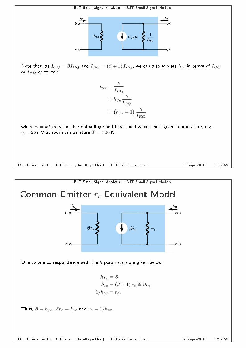
BJT Small-Signal Analysis BJT Small-Signal Models
Common-Emitter re Equivalent Model
One-to-one correspondence with the h-parameters are given below,
hfe = β
hie = (β + 1) re ∼= βre
1/hoe = ro.
Thus, β = hfe, βre = hie and ro = 1/hoe.
Dr. U. Sezen & Dr. D. Gökcen (Hacettepe Uni.) ELE230 Electronics I 21-Apr-2018 12 / 59
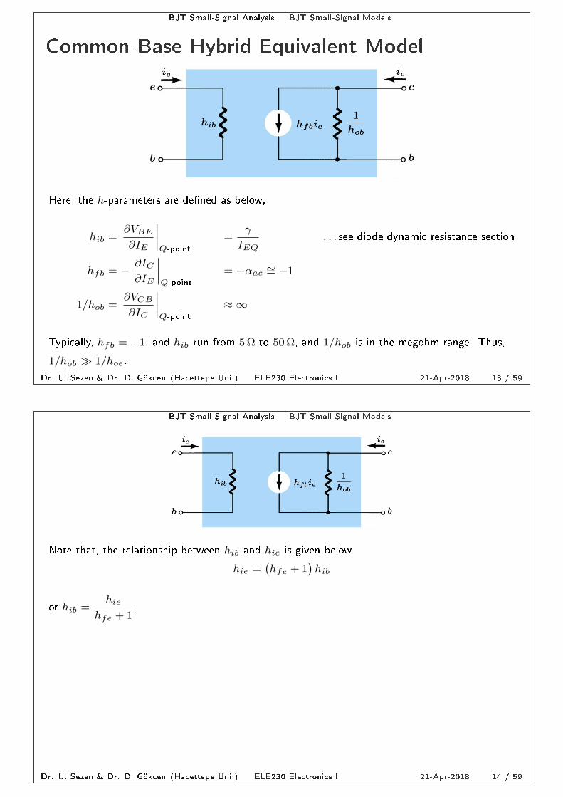
BJT Small-Signal Analysis BJT Small-Signal Models
Common-Base Hybrid Equivalent Model
Here, the h-parameters are dened as below,
hib =∂VBE
∂IE
∣∣∣∣Q-point
=γ
IEQ. . . see diode dynamic resistance section
hfb = −∂IC
∂IE
∣∣∣∣Q-point
= −αac∼= −1
1/hob =∂VCB
∂IC
∣∣∣∣Q-point
≈ ∞
Typically, hfb = −1, and hib run from 5 Ω to 50 Ω, and 1/hob is in the megohm range. Thus,
1/hob 1/hoe.
Dr. U. Sezen & Dr. D. Gökcen (Hacettepe Uni.) ELE230 Electronics I 21-Apr-2018 13 / 59
BJT Small-Signal Analysis BJT Small-Signal Models
Note that, the relationship between hib and hie is given below
hie =(hfe + 1
)hib
or hib =hie
hfe + 1.
Dr. U. Sezen & Dr. D. Gökcen (Hacettepe Uni.) ELE230 Electronics I 21-Apr-2018 14 / 59

BJT Small-Signal Analysis BJT Small-Signal Models
Common-Base re Equivalent Model
One-to-one correspondence with the h-parameters are given below
hfb = −αhib = re
1/hob = ro.
Thus, α = −hfb ∼= 1, re = hib and ro = 1/hob ∼=∞. Note that, minus sign is due to the
direction of the current source.
Dr. U. Sezen & Dr. D. Gökcen (Hacettepe Uni.) ELE230 Electronics I 21-Apr-2018 15 / 59
BJT Small-Signal Analysis BJT Small-Signal Models
Phase Relationship
The phase relationship between input and output depends on the amplier conguration circuitas listed below.
Common-Emitter: 180 degrees
Common-Base: 0 degrees
Common-Collector: 0 degrees (Emitter-Follower)
Dr. U. Sezen & Dr. D. Gökcen (Hacettepe Uni.) ELE230 Electronics I 21-Apr-2018 16 / 59

BJT Small-Signal Analysis Common-Emitter Fixed-Bias Conguration
Common-Emitter Fixed-Bias Conguration
Common-emitter xed-bias conguration is given below
Let us start SSAC analysis by drawing the AC equivalent circuit as shown below
Dr. U. Sezen & Dr. D. Gökcen (Hacettepe Uni.) ELE230 Electronics I 21-Apr-2018 17 / 59
BJT Small-Signal Analysis Common-Emitter Fixed-Bias Conguration
Then, we are going to replace BJT with its common-emitter hybrid equivalent model asshown below
Obtain hfe and 1/hoe from the specication sheet of the transistor or by testing thetransistor using a curve tracer. Calculate hie using the DC analysis values as
hie =26mV
IBQ= hfe
26mV
ICQ.
Dr. U. Sezen & Dr. D. Gökcen (Hacettepe Uni.) ELE230 Electronics I 21-Apr-2018 18 / 59

BJT Small-Signal Analysis Common-Emitter Fixed-Bias Conguration
Input Resistance
Input resistance Ri is given as
Ri =vi
ii
∣∣∣∣RL=∞
= RB ||hie
If RB ≥ 10hie, then Ri simplies to Ri = hie.
Input resistance Ri according to the re model is given by
Ri = RB ||βre
Dr. U. Sezen & Dr. D. Gökcen (Hacettepe Uni.) ELE230 Electronics I 21-Apr-2018 19 / 59
BJT Small-Signal Analysis Common-Emitter Fixed-Bias Conguration
Voltage Gain
No-load voltage gain Av is given by
Av =vo
vi
∣∣∣∣RL=∞
=
(vo
hfeib
)(hfeib
ib
)(ib
vi
)= (−RC ||1/hoe)
(hfe
)( 1
hie
)= −
hfe (RC ||1/hoe)
hie
No-load voltage gain Av according to the re model is given by
Av = −RC ||rore
Dr. U. Sezen & Dr. D. Gökcen (Hacettepe Uni.) ELE230 Electronics I 21-Apr-2018 20 / 59

BJT Small-Signal Analysis Common-Emitter Fixed-Bias Conguration
If 1/hoe ≥ 10RC , no-load voltage gain Av reduces to
Av = −hfeRC
hie. . . re model: Av = −
RC
re
For the circuit above, we can obtain the current gain Ai as follows
Ai =io
ii=vo/RC
vi/Ri=
Ri
RC
vo
vi
=Ri
RCAv
If 1/hoe ≥ 10RC and RB ≥ 10hie, current gain Ai reduces to
Ai = −hfe . . . re model: Ai = −β
Dr. U. Sezen & Dr. D. Gökcen (Hacettepe Uni.) ELE230 Electronics I 21-Apr-2018 21 / 59
BJT Small-Signal Analysis Common-Emitter Fixed-Bias Conguration
Output Resistance
Output resistance, i.e., Thévenin equivalent resistance, Ro is calculated using the testvoltage circuit above. Note that in the circuit ib = 0, so hfeib = 0 as well.
Ro =vtest
itest
∣∣∣∣vs=0,RL=vtest
= RC ||1/hoe
If 1/hoe ≥ 10RC , then Ro simplies to Ro = RC .
Output resistance Ro according to the re model is given by
Ro = RC ||ro
Dr. U. Sezen & Dr. D. Gökcen (Hacettepe Uni.) ELE230 Electronics I 21-Apr-2018 22 / 59

BJT Small-Signal Analysis Common-Emitter Fixed-Bias Conguration
Phase Relationship
The phase relationship between input and output is 180 degrees as shown above.
The negative sign used in the voltage gain formulas indicates the inversion.
Dr. U. Sezen & Dr. D. Gökcen (Hacettepe Uni.) ELE230 Electronics I 21-Apr-2018 23 / 59
BJT Small-Signal Analysis Common-Emitter Voltage-Divider Bias Conguration
CE Voltage-Divider Bias CongurationCommon-emitter voltage-divider bias conguration is given below
Corresponding SSAC equivalent circuit is shown below
Dr. U. Sezen & Dr. D. Gökcen (Hacettepe Uni.) ELE230 Electronics I 21-Apr-2018 24 / 59

BJT Small-Signal Analysis Common-Emitter Voltage-Divider Bias Conguration
Input Resistance
Input resistance Ri is given as
Ri =vi
ii
∣∣∣∣RL=∞
= R1||R2||hie
Input resistance Ri according to the re model is given by
Ri = R1||R2||βre
Dr. U. Sezen & Dr. D. Gökcen (Hacettepe Uni.) ELE230 Electronics I 21-Apr-2018 25 / 59
BJT Small-Signal Analysis Common-Emitter Voltage-Divider Bias Conguration
Voltage Gain
No-load voltage gain Av is given by
Av =vo
vi
∣∣∣∣RL=∞
=
(vo
hfeib
)(hfeib
ib
)(ib
vi
)= (−RC ||1/hoe)
(hfe
)( 1
hie
)= −
hfe (RC ||1/hoe)
hie
No-load voltage gain Av according to the re model is given by
Av = −RC ||rore
Dr. U. Sezen & Dr. D. Gökcen (Hacettepe Uni.) ELE230 Electronics I 21-Apr-2018 26 / 59

BJT Small-Signal Analysis Common-Emitter Voltage-Divider Bias Conguration
If 1/hoe ≥ 10RC , no-load voltage gain Av reduces to
Av = −hfeRC
hie. . . re model: Av = −
RC
re
For the circuit above, we can obtain the current gain Ai as follows
Ai =io
ii=vo/RC
vi/Ri=
Ri
RC
vo
vi
=Ri
RCAv
If 1/hoe ≥ 10, and given R′ = R1||R2, current gain Ai reduces to
Ai = −hfeR′
R′ + hie. . . re model: Ai = −
R′
R′/β + re
Dr. U. Sezen & Dr. D. Gökcen (Hacettepe Uni.) ELE230 Electronics I 21-Apr-2018 27 / 59
BJT Small-Signal Analysis Common-Emitter Voltage-Divider Bias Conguration
Output Resistance
Output resistance, i.e., Thévenin equivalent resistance, Ro is calculated using the testvoltage circuit above. Note that in the circuit ib = 0, so hfeib = 0 as well.
Ro =vtest
itest
∣∣∣∣vs=0,RL=vtest
= RC ||1/hoe
If 1/hoe ≥ 10RC , then Ro simplies to Ro = RC .
Output resistance Ro according to the re model is given by
Ro = RC ||ro
Dr. U. Sezen & Dr. D. Gökcen (Hacettepe Uni.) ELE230 Electronics I 21-Apr-2018 28 / 59

BJT Small-Signal Analysis Common-Emitter Voltage-Divider Bias Conguration
Phase Relationship
Phase relationship between input and output of a common-emitter amplier congurationif always 180 degrees. This is independent of the type of the bias-conguration.
Dr. U. Sezen & Dr. D. Gökcen (Hacettepe Uni.) ELE230 Electronics I 21-Apr-2018 29 / 59
BJT Small-Signal Analysis Common-Emitter Unbypassed-Emitter Bias Conguration
CE Unbypassed-Emitter Bias Conguration
Common-emitter unbypassed-emitter bias conguration and its SSAC equivalent circuitare given on the left and right gures below, respectively.
When RE is not bypassed, we normally assume 1/hoe =∞ in order to reduce thecalculation complexity. Because of the feedback, even 1/hoe 6=∞ the results do not reallychange at all.
Dr. U. Sezen & Dr. D. Gökcen (Hacettepe Uni.) ELE230 Electronics I 21-Apr-2018 30 / 59

BJT Small-Signal Analysis Common-Emitter Unbypassed-Emitter Bias Conguration
Input Resistance
Input resistance Ri is given as
Ri =vi
ii
∣∣∣∣RL=∞
= RB ||Rb . . . Rb = hie +(hfe + 1
)RE
= RB ||[hie +
(hfe + 1
)RE
]Input resistance Ri according to the re model is given by
Ri = RB || (β + 1) (re +RE) ∼= RB ||β (re +RE)
Dr. U. Sezen & Dr. D. Gökcen (Hacettepe Uni.) ELE230 Electronics I 21-Apr-2018 31 / 59
BJT Small-Signal Analysis Common-Emitter Unbypassed-Emitter Bias Conguration
Voltage Gain
No-load voltage gain Av is given by
Av =vo
vi
∣∣∣∣RL=∞
=
(vo
hfeib
)(hfeib
ib
)(ib
vi
)= (−RC)
(hfe
)( 1
Rb
)= −
hfeRC
hie +(hfe + 1
)RE
No-load voltage gain Av according to the re model is given by
Av = −RC
re +RE
Dr. U. Sezen & Dr. D. Gökcen (Hacettepe Uni.) ELE230 Electronics I 21-Apr-2018 32 / 59
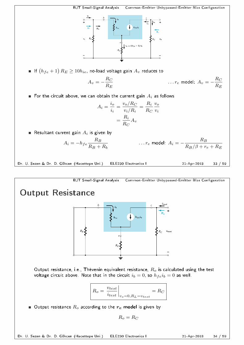
BJT Small-Signal Analysis Common-Emitter Unbypassed-Emitter Bias Conguration
If(hfe + 1
)RE ≥ 10hie, no-load voltage gain Av reduces to
Av = −RC
RE. . . re model: Av = −
RC
RE
For the circuit above, we can obtain the current gain Ai as follows
Ai =io
ii=vo/RC
vi/Ri=
Ri
RC
vo
vi
=Ri
RCAv
Resultant current gain Ai is given by
Ai = −hfeRB
RB +Rb. . . re model: Ai = −
RB
RB/β + re +RE
Dr. U. Sezen & Dr. D. Gökcen (Hacettepe Uni.) ELE230 Electronics I 21-Apr-2018 33 / 59
BJT Small-Signal Analysis Common-Emitter Unbypassed-Emitter Bias Conguration
Output Resistance
Output resistance, i.e., Thévenin equivalent resistance, Ro is calculated using the testvoltage circuit above. Note that in the circuit ib = 0, so hfeib = 0 as well.
Ro =vtest
itest
∣∣∣∣vs=0,RL=vtest
= RC
Output resistance Ro according to the re model is given by
Ro = RC
Dr. U. Sezen & Dr. D. Gökcen (Hacettepe Uni.) ELE230 Electronics I 21-Apr-2018 34 / 59

BJT Small-Signal Analysis Common-Emitter Unbypassed-Emitter Bias Conguration
Phase Relationship
Phase relationship between input and output of a common-emitter amplier congurationif always 180 degrees. This is independent of the type of the bias-conguration.
Dr. U. Sezen & Dr. D. Gökcen (Hacettepe Uni.) ELE230 Electronics I 21-Apr-2018 35 / 59
BJT Small-Signal Analysis Emitter-Follower Conguration
Emitter-Follower Conguration
Emitter-follower (common-collector) conguration and its SSAC equivalent circuit aregiven on the left and right gures below, respectively.
When RE is not bypassed, we normally assume 1/hoe =∞ in order to reduce thecalculation complexity.
Dr. U. Sezen & Dr. D. Gökcen (Hacettepe Uni.) ELE230 Electronics I 21-Apr-2018 36 / 59

BJT Small-Signal Analysis Emitter-Follower Conguration
Input Resistance
Input resistance Ri is given as
Ri =vi
ii
∣∣∣∣RL=∞
= RB ||Rb . . . Rb = hie +(hfe + 1
)RE
= RB ||[hie +
(hfe + 1
)RE
]Input resistance Ri according to the re model is given by
Ri = RB || (β + 1) (re +RE) ∼= RB ||β (re +RE)
Dr. U. Sezen & Dr. D. Gökcen (Hacettepe Uni.) ELE230 Electronics I 21-Apr-2018 37 / 59
BJT Small-Signal Analysis Emitter-Follower Conguration
Voltage Gain
No-load voltage gain Av is given by
Av =vo
vi
∣∣∣∣RL=∞
=
(vo
ib
)(ib
vi
)=
[(hfe + 1
)RE
]( 1
Rb
). . . Rb = hie +
(hfe + 1
)RE
=
(hfe + 1
)RE
hie +(hfe + 1
)RE
∼= 1
No-load voltage gain Av according to the re model is given by
Av =RE
re +RE
∼= 1
Dr. U. Sezen & Dr. D. Gökcen (Hacettepe Uni.) ELE230 Electronics I 21-Apr-2018 38 / 59

BJT Small-Signal Analysis Emitter-Follower Conguration
For the circuit above, we can obtain the current gain Ai as follows
Ai =io
ii=vo/RE
vi/Ri=
Ri
RE
vo
vi
=Ri
REAv
Resultant current gain Ai is given by,
Ai =(hfe + 1
) RB
RB +Rb. . . re model: Ai =
RB
RB/ (β + 1) + re +RE
Dr. U. Sezen & Dr. D. Gökcen (Hacettepe Uni.) ELE230 Electronics I 21-Apr-2018 39 / 59
BJT Small-Signal Analysis Emitter-Follower Conguration
Output Resistance
Output resistance, i.e., Thévenin equivalent resistance, Ro is calculated using the testvoltage circuit above.
Ro =vtest
itest
∣∣∣∣vs=0,RL=vtest
= RE ||hie
hfe + 1
Output resistance Ro according to the re model is given by
Ro = RE ||reIf 1/hoe 6=∞, then replace RE with (RE ||1/hoe) in Ri, Av and Ro calculations.
If a voltage source with source resistance Rs is connected to the input, replace hie with(hie +RB ||Rs) in Ro calculations.
Dr. U. Sezen & Dr. D. Gökcen (Hacettepe Uni.) ELE230 Electronics I 21-Apr-2018 40 / 59

BJT Small-Signal Analysis Emitter-Follower Conguration
Phase Relationship
Emitter-follower (common-collector) conguration has no phase shift between input andoutput.
Dr. U. Sezen & Dr. D. Gökcen (Hacettepe Uni.) ELE230 Electronics I 21-Apr-2018 41 / 59
BJT Small-Signal Analysis Common-Emitter Collector Feedback Conguration
CE Collector Feedback CongurationCommon-emitter collector feedback bias conguration is given below
Corresponding SSAC equivalent circuit is shown below
Dr. U. Sezen & Dr. D. Gökcen (Hacettepe Uni.) ELE230 Electronics I 21-Apr-2018 42 / 59

BJT Small-Signal Analysis Common-Emitter Collector Feedback Conguration
Input Resistance
Input resistance Ri is given as
Ri =vi
ii
∣∣∣∣RL=∞
=hie
1 +hie+hfeRC
RF+RC
. . . if = −hie + hfeRC
RF +RCib
∼=hie
1 +hfeRC
RF +RC
. . . hfeRC hie
Input resistance Ri according to the re model is given by
Ri∼=
βre
1 +βRC
RF +RC
Dr. U. Sezen & Dr. D. Gökcen (Hacettepe Uni.) ELE230 Electronics I 21-Apr-2018 43 / 59
BJT Small-Signal Analysis Common-Emitter Collector Feedback Conguration
Voltage Gain
No-load voltage gain Av is given by
Av =vo
vi
∣∣∣∣RL=∞
=
(hfeRF − hieRF +RC
)(−RC
hie
). . . if = −
hie + hfeRC
RF +RCib
∼=(
hfeRF
RF +RC
)(−RC
hie
). . . hfeRF hie
≈ −hfeRC
hie. . . RF RC
No-load voltage gain Av according to the re model is given by
Av ≈ −RC
re
Dr. U. Sezen & Dr. D. Gökcen (Hacettepe Uni.) ELE230 Electronics I 21-Apr-2018 44 / 59

BJT Small-Signal Analysis Common-Emitter Collector Feedback Conguration
For the circuit above, we can obtain the current gain Ai as follows
Ai =io
ii=vo/RC
vi/Ri=
Ri
RC
vo
vi
=Ri
RCAv
Resultant current gain Ai is given by,
Ai∼= −
hfe (RF +RC)
RF +(hfe + 1
)RC
. . . re model: Ai = −RF +RC
RF /β +RC
Dr. U. Sezen & Dr. D. Gökcen (Hacettepe Uni.) ELE230 Electronics I 21-Apr-2018 45 / 59
BJT Small-Signal Analysis Common-Emitter Collector Feedback Conguration
Output Resistance
Output resistance, i.e., Thévenin equivalent resistance, Ro is calculated using the testvoltage circuit above. Note that in the circuit ib = 0, so hfeib = 0 as well.
Ro =vtest
itest
∣∣∣∣vs=0,RL=vtest
= RC ||RF
Output resistance Ro according to the re model is given by
Ro = RC ||RF
If 1/hoe 6=∞, then replace RC with (RC ||1/hoe) in Ri, Av and Ro calculations.
If a voltage source with source resistance Rs is connected to the input, replace RF with[RF (Rs + hie) /
(hfeRs + hie
)]in Ro calculations.
Dr. U. Sezen & Dr. D. Gökcen (Hacettepe Uni.) ELE230 Electronics I 21-Apr-2018 46 / 59

BJT Small-Signal Analysis Common-Emitter Collector Feedback Conguration
Phase Relationship
Phase relationship between input and output of a common-emitter amplier congurationif always 180 degrees. This is independent of the type of the bias-conguration.
Dr. U. Sezen & Dr. D. Gökcen (Hacettepe Uni.) ELE230 Electronics I 21-Apr-2018 47 / 59
BJT Small-Signal Analysis Common-Base Conguration
Common-Base Conguration
Common-base conguration is given below
Corresponding SSAC equivalent circuit is shown below
Here, hib =hie
hfe + 1=
26mV
IEQand hfb = −αac = −1.
Dr. U. Sezen & Dr. D. Gökcen (Hacettepe Uni.) ELE230 Electronics I 21-Apr-2018 48 / 59

BJT Small-Signal Analysis Common-Base Conguration
Input Resistance
Input resistance Ri is given as
Ri =vi
ii
∣∣∣∣RL=∞
= RE ||hib
If RE ≥ 10hib, then Ri simplies to Ri = hib.
Input resistance Ri according to the re model is given by
Ri = RE ||re
Dr. U. Sezen & Dr. D. Gökcen (Hacettepe Uni.) ELE230 Electronics I 21-Apr-2018 49 / 59
BJT Small-Signal Analysis Common-Base Conguration
Voltage Gain
No-load voltage gain Av is given by
Av =vo
vi
∣∣∣∣RL=∞
=
(vo
hfbie
)(hfbie
ie
)(ie
vi
)= (−RC)
(hfb
)( 1
hib
)=RC
hib. . . hfb = −1
No-load voltage gain Av according to the re model is given by
Av =RC
re
Dr. U. Sezen & Dr. D. Gökcen (Hacettepe Uni.) ELE230 Electronics I 21-Apr-2018 50 / 59

BJT Small-Signal Analysis Common-Base Conguration
For the circuit above, we can obtain the current gain Ai as follows
Ai =io
ii=vo/RC
vi/Ri=
Ri
RC
vo
vi
=Ri
RCAv
Resultant current gain Ai is given by,
Ai =RE ||hibhib
≈ 1 . . . re model: Ai =RE ||rere
≈ 1
Dr. U. Sezen & Dr. D. Gökcen (Hacettepe Uni.) ELE230 Electronics I 21-Apr-2018 51 / 59
BJT Small-Signal Analysis Common-Base Conguration
Output Resistance
Output resistance, i.e., Thévenin equivalent resistance, Ro is calculated using the testvoltage circuit above. Note that in the circuit ie = 0, so hfbie = 0 as well.
Ro =vtest
itest
∣∣∣∣vs=0,RL=vtest
= RC
Output resistance Ro according to the re model is given by
Ro = RC
If 1/hob 6=∞, then replace RC with (RC ||1/hob) in Ri, Av and Ro calculations.
Dr. U. Sezen & Dr. D. Gökcen (Hacettepe Uni.) ELE230 Electronics I 21-Apr-2018 52 / 59

BJT Small-Signal Analysis Common-Base Conguration
Phase Relationship
A common-base amplier conguration has no phase shift between input and output
Dr. U. Sezen & Dr. D. Gökcen (Hacettepe Uni.) ELE230 Electronics I 21-Apr-2018 53 / 59
BJT Small-Signal Analysis Common-Base Conguration
Example 1: Consider the common-base BJT amplier in the gure above.
a) Perform DC analysis and nd the Q-point.b) Evaluate the overall voltage gain AVs and the current gain Ai.c) Sketch vo on the AC+DC load line graph when
i. vs = 100 sin (ωt) mV,ii. vs = 900 sin (ωt) mV.
Dr. U. Sezen & Dr. D. Gökcen (Hacettepe Uni.) ELE230 Electronics I 21-Apr-2018 54 / 59

BJT Small-Signal Analysis Common-Base Conguration
Solution: a) Let us rst draw the DC equivalent circuit rst as shown below,
Here, RE = RE1 +RE2 = 0.2k + 1.5k = 1.7 kΩ.
Now, let us calculate VBB , RBB , ICQ, VCEQ and VCBQ
VBB =
(30k
30k + 180k
)(10) = 1.43V,
RBB = 30k||180k = 25.71 kΩ,
ICQ∼= IEQ =
1.43− 0.7
25.71k/201 + 1.7k= 0.4mA,
VCEQ = 10− (0.4m)(4.7k + 1.7k) = 7.44V,
VCBQ = 7.44− 0.7 = 6.74V.
Dr. U. Sezen & Dr. D. Gökcen (Hacettepe Uni.) ELE230 Electronics I 21-Apr-2018 55 / 59
BJT Small-Signal Analysis Common-Base Conguration
b) In order to calculate the voltage gain, we need to draw the common-base SSACequivalent circuit. As it is not given 1/hob =∞. Let us now calculate hib as
hib =26m
0.4m= 65 Ω.
So, the small-signal equivalent circuit is given below
Now, let us calculate input resistance Ri and voltage gain with load AV as follows
Ri = RE2|| (RE1 + hib) = 1.5k||(200 + 65) ∼= 225 Ω
AV =vo
vi=
(vo
hfbie
)(hfbie
ie
)(ie
vi
)= (−RC ||RL)
(hfb
)( 1
RE1+ hib
)=
RC ||RL
RE1+ hib
=4.7k||10k
200 + 65=
3.2k
0.265k= 12.08.
Dr. U. Sezen & Dr. D. Gökcen (Hacettepe Uni.) ELE230 Electronics I 21-Apr-2018 56 / 59

BJT Small-Signal Analysis Common-Base Conguration
Thus, overall voltage gain AVs and current gain Ai are given by
AVs =vo
vs=
(vo
vi
)(vi
vs
)= AV
Ri
Rs + Ri
= (12.08)
(225
100 + 225
)= 8.36,
Ai =io
ii=
vo/RL
vi/Ri
= AVRi
RL
= (12.08)
(0.225k
10k
)= 0.27.
c) Let us write down the AC load line equation for this common-base amplier, noting that
vo = vcb = −ic(RC ||RL) = −icRac and vcb = vce − vbe = vce −hib
RE1+hib
vi ≈ vce)
vCB = −iCRac + VCBQ + ICQRac . . . VCBQ = VCEQ − VBEQ
vCE − VBEQ = −iCRac + VCEQ − VBEQ + ICQRac . . . vCB ≈ vCE − VBEQ
vCE = −iCRac + VCEQ + ICQRac
So, Rac = RC ||RL = 4.7k||10k = 3.2 kΩ, and similarly we obtain RDC from the C-E loop asRDC = RC + RE = 4.7k + 1.7k = 6.4 kΩ.
Dr. U. Sezen & Dr. D. Gökcen (Hacettepe Uni.) ELE230 Electronics I 21-Apr-2018 57 / 59
BJT Small-Signal Analysis Common-Base Conguration
Note that, maximum available undistorted swing amplitude ismin
(VCEQ, ICQRac
)= min(7.44, (0.4m)(3.2k)) = min(7.44, 1.28) = 1.28V.
Thus, as AVs = 8.36, maximum input source amplitude which gives an undistorted outputis max(vs(p)) = 1.28/8.36 = 153.1mV. If the input source amplitude exceeds this value,we will observe distortion at the output.
i. For vs = 100 sin (ωt) mV, we are going to observe an undistorted sinusoidal outputwith an amplitude of 0.836V around VCBQ = 6.74V as shown below.
Dr. U. Sezen & Dr. D. Gökcen (Hacettepe Uni.) ELE230 Electronics I 21-Apr-2018 58 / 59

BJT Small-Signal Analysis Common-Base Conguration
ii. For vs = 900 sin (ωt) mV, we are going to observe a distorted output as shown below.
Dr. U. Sezen & Dr. D. Gökcen (Hacettepe Uni.) ELE230 Electronics I 21-Apr-2018 59 / 59