by dissertation doctor of philosophy engineering
TRANSCRIPT

VLSI Design Techniques for Floating-Point Computation
By
Bidyut Kumar Bose
B.Tech. (Indian Institute of Technology) 1977
M.S. (Carnegie-Mellon University) 1979
DISSERTATION
Submitted in partial satisfaction of the requirements for the degree of
DOCTOR OF PHILOSOPHY
in
ENGINEERING
ELECTRICAL ENGINEERING AND COMPUTER SCIENCE
in the
GRADUATE DMSION
of the
UNIVERSITY OF CALIFORNIA at BERKELEY
Appro·.·~= .... 1>. :c~· ... ?.~~ .................. ·/~]!~~- .. .. .... /~a ....................... /1 ....... .
' -:/ _,...- ' ,-~..,._-·"· I
1/i~---/ ,'/. (_; /---/..:._-. //.< i,· .
• ' ... < -. ·• ". • • J..,. • • • • • ~ • --;-' • -. • • • • • • • • • • • • • • • • • • • • • • • • ' " .' ;-- ~//• • \ • . • • •
**********************************

Report Documentation Page Form ApprovedOMB No. 0704-0188
Public reporting burden for the collection of information is estimated to average 1 hour per response, including the time for reviewing instructions, searching existing data sources, gathering andmaintaining the data needed, and completing and reviewing the collection of information. Send comments regarding this burden estimate or any other aspect of this collection of information,including suggestions for reducing this burden, to Washington Headquarters Services, Directorate for Information Operations and Reports, 1215 Jefferson Davis Highway, Suite 1204, ArlingtonVA 22202-4302. Respondents should be aware that notwithstanding any other provision of law, no person shall be subject to a penalty for failing to comply with a collection of information if itdoes not display a currently valid OMB control number.
1. REPORT DATE NOV 1988 2. REPORT TYPE
3. DATES COVERED 00-00-1988 to 00-00-1988
4. TITLE AND SUBTITLE VLSI Design Techniques for Floating-Point Computation
5a. CONTRACT NUMBER
5b. GRANT NUMBER
5c. PROGRAM ELEMENT NUMBER
6. AUTHOR(S) 5d. PROJECT NUMBER
5e. TASK NUMBER
5f. WORK UNIT NUMBER
7. PERFORMING ORGANIZATION NAME(S) AND ADDRESS(ES) University of California at Berkeley,Department of ElectricalEngineering and Computer Sciences,Berkeley,CA,94720
8. PERFORMING ORGANIZATIONREPORT NUMBER
9. SPONSORING/MONITORING AGENCY NAME(S) AND ADDRESS(ES) 10. SPONSOR/MONITOR’S ACRONYM(S)
11. SPONSOR/MONITOR’S REPORT NUMBER(S)
12. DISTRIBUTION/AVAILABILITY STATEMENT Approved for public release; distribution unlimited
13. SUPPLEMENTARY NOTES
14. ABSTRACT This thesis presents design techniques for floating-point computation in VLSI. A basis for area-time designdecisions for arithmetic and memory operations is formulated from a study of computationally intensiveprograms. Tradeoffs in the design and implementation of an efficient coprocessor interface are studied,together with the implications of hardware support for the IEEE Floating-Point Standard. Algorithmarea-time tradeoffs for basic arithmetic functions are analyzed in light of changing technology. Details of asingle-chip floating-point unit designed into two micron CMOS for SPUR are described, including specialdesign considerations for very wide datapaths. The pervasive effects of scaling technology on differentlevels of design are explored, from devices and circuits, through logic and micro-architecture, toalgorithms and systems.
15. SUBJECT TERMS
16. SECURITY CLASSIFICATION OF: 17. LIMITATION OF ABSTRACT Same as
Report (SAR)
18. NUMBEROF PAGES
186
19a. NAME OFRESPONSIBLE PERSON
a. REPORT unclassified
b. ABSTRACT unclassified
c. THIS PAGE unclassified
Standard Form 298 (Rev. 8-98) Prescribed by ANSI Std Z39-18

VLSI Design Techniques for Floating-Point Computation
Bidyut Kumar Bose
Abstract
This thesis presents design techniques for floating-point computation m
VLSI. A basis for area-time design decisions for arithmetic and memory
operations is formulated from a study of computationally intensive programs.
Tradeoffs in the design and implementation of an efficient coprocessor inter-
face are studied, together with the implications of hardware support for the
IEEE Floating-Point Standard. Algorithm area-time tradeoffs for basic arith-
metic functions are analyzed in light of changing technology. Details of a
single-chip floating-point unit designed in two micron CMOS for SPUR are
described, including special design considerations for very wide datapaths.
The pervasive effects of scaling technology on different levels of design are
explored, from devices and circuits, through logic and micro-architecture, to
algorithms and systems.
David A. Patterson (Committee Chairman)
1

11
Dedicated with love to
-- Baba Ma Joya Didi Tutul--


iii
Acknowledgement
This work would not have been completed without the constant, selfless love and gentle
encouragement of my parents, my best-buddy Joya, and my sisters Krishna and Devjani.
Dave Patterson, my research advisor, has been invaluable with his guidance, advice and
support, and Dave Hodges and Bob Goldman kindly served on my dissertation commit
tee. A project of this scope would have been impossible without the essential contribu
tions of many colleagues, including the completion and testing of the FPU functional
simulator by Corinna Lee, the coprocessor interface specification by Paul Hansen, and
layout, circuit, and timing simulation of portions of the FPU datapath and control by Tim
Hu and Debby Jensen. Principal funding for the project was by DARPA under contract
N00039-85-C-0269.

iv
Table of Contents
CHAPTER 1. Introduction .................................................................................. 1
1.1. Motivation . .. .. ....... .. .. .. ... .. .. .. .. ... .. .. .. .. . . ... .. .... .. ... .... .... .. ... .. .. .. ......... .... .. . 2 1.2. Thesis Outline .. .... .... ..... .. .. .. .. ... .. .. .. .. .. ... .... .. ..... .. .. .. .. .. ... .. .... .. ..... .... ..... 6 1.3. References ........................................................................................... 9
CHAPTER 2. Floating-point Computation Characteristics & Accelerators 10
2.1. Characteristics of Floating-point Computation ................................ 11 2.1.1. Frequently Used Functions ............................................................ 11 2.1.2. Two Benchmarks, Linpack and Livermore Loops ..................... ... 13 2.1.3. Dynamic Data From Two Real Programs ...................................... 17 2.2. Comparison of Floating-point Processors ......................................... 20 2.2.1. Comprehensive Floating-point Processors .................................... 21 2.2.2. Basic Floating-point Processors .... ....... .... ...................................... 22 2.2.3. Floating-point Performance Comparison ....................................... 24 2.3. Summary ........................................................................................... 27 2.4. References ......................................................................................... 29
CHAPTER 3. Design Tradeoffs for VLSI Floating-Point Units ..................... 30
3.1. Coprocessor Interface Design ........................................... .. ..... ...... .. . 32 3.1.1. Communication Overhead in Floating-Point Coprocessors .......... 33 3.1.2. Communication Overhead and Total Loop Execution Time .. .. ..... 34 3.1.3. Parallel Execution Between CPU and FPU ................................... 39 3.2. Implementing the IEEE Floating-Point Standard ............................. 42 3.2.1. Data Formats .................................................................................. 42 3.2.2. Memory and Arithmetic Operations .. .... .... ..... ........ ....... .... ... .. .... .. . 44 3.2.3. Exception Detection and Handling ................................................ 46 3.3. Arithmetic Algorithms and Implementation Technology ................. 48 3.3.1. Add/Subtract Design Issues ........................................................... 50 3.3.2. Multiply Design Issues .................................................................. 52 3.3.3. Divide Design Issues ...................................................................... 55 3.4. Summary ........................................................................................... 57 3.5. References ......................................................................................... 59

v
CHAPTER 4. Add/Subtract Datapath Design Considerations ...... ................ 61
4.1. Implementation Considerations .................. ...................................... 62 4.2. The Exponent & Fraction Front-Ends ............................................... 64 4.2.1. Unpacking and Packing Data ......................................................... 66 4.2.2. Handling Special Operands ............................................................ 67 4.2.3. Conversion to Single and Double Precision .................................. 68 4.2.4. The Register File ............................................................................ 68 4.3. The Exponent Datapath ..................................................................... 71 4.3.1. The Exponent Difference Unit ....................................................... 73 4.3.1.1. A Fast Adder/Subtractor ............................................................. 73 4.3.2. Overflow and Underflow Detection ............................................... 78 4.4. The Fraction Datapath ....................................................................... 79 4.4.1. The Shifter ..................................................................................... 82 4.4.1.1. The Shifter Array ........................................................................ 83 4.4.1.2. The Sticky Logic ............. ........... ................................................. 84 4.4.1.3. The Shifter Decoder .................................................................... 85 4.4.2. The Leading One's Detector .......................................................... 88 4.5. Rounding ........................................................................................... 89 4.6. Summary ........................................................................................... 91 4.7. References ......................................................................................... 93
CHAPTERS. Multiply/Divide Datapath Design Considerations ................... 94
5.1. Implementation Considerations ........................................................ 95 5.2. The Multiplier ................................................................................... 97 5.2.1. The Algorithm ................................................................................ 97 5.2.2. The Multiply Inner Loop ............................................................... 99 5.2.3. Rounding ...................................................................................... 101 5.3. The Divider ..................................................................................... 104 5.3.1. The Algorithm .............................................................................. 104 5.3.2. The Divide Inner Loop ................................................................. 106 5.3.3. Quotient Selection ........................................................................ 108 5.3.4. Rounding ...................................................................................... 109 5.4. Summary ......................................................................................... 111 5.5. References . .. .. ... .. .. .. .. .. .... . .. .. .. .... . .. .. .. .. .. . .. .. .. .. ... .. .. .. .. .. .... ... .. .. ... .. .. .. . 113
CHAPTER 6. Control Design Considerations ............................................... 114
6.1. FPU Control Unit Overview ........................................................... 115 6.2. The Instruction Decoder ...... ...................... .... ...................... ............ 116 6.3. Load-Store Control ......................................................................... 118 6.4. Arithmetic Control .......................................................................... 120 6.4.1. The State Machine ....................................................................... 121
vi
6.4.2. The Cycle Counter ....................................................................... 123 6.4.3. PLA Partitioning .......................................................................... 124 6.5. Clock Generation, Distribution and Skew ...................................... 125 6.6. Swnmary ......................................................................................... 135 6. 7. References . .. .. ... .. .. .. .. ....... ......... .. .. .. .. .. ... .. .. .... ..... .. .. .. .. ... .. .... .. ... .. .. . . . 137
CHAPTER 7. Implications of Scaling Technology ....................................... 138
7 .I. Scaling at the Device/Circuit Level . ..... .. . . .. .. ..... .. .. .. .. ..... .. .. .. .. . .. .. ... 139 7.2. Scaling at the Logic/Micro-architectural Level .............................. 141 7.3. Scaling and Arithmetic Algorithms ................................................ 143 7.4. Scaling and Multiple Function Units .............................................. 147 7.5. Scaling at the Architectural Level .................................................. 151 7.6. Swnmary ......................................................................................... 154 7.7. References ....................................................................................... 156
CHAPTER 8. Conclusions ............................................................................... 158
8.1. Swnmary ......................................................................................... 158 8.2. Future Work .................................................................................... 162 8.3. References ....................................................................................... 164
APPENDICES 167
Appendix 1. SPUR FPU die photograph ............................................... 168 Appendix 2. SPUR FPU Instruction Set and Cycle Times .... .. .. ..... .. .. .. . 169 Appendix 3. SPUR FPU Timing Wavefonns ........................................ 170

1
1 Introduction
From their very inception, computers have been driven by the forcing function of
scientific computation towards ever higher performance. Since scientific and engineering
computations are dominated by floating-point calculations, these have had to be speeded
up to sustain the drive for higher performance. The evolution of VLSI technology
towards finer geometries has been another dominant factor in performance improvement.
This in turn has precipitated a need for the evolution of design techniques for efficient
implementation of floating-point arithmetic in VLSI. This thesis develops design tech
niques for fast floating-point computation in VLSI.

Chapter 1 2
Computationally intensive programs are studied to formulate a basis for area-time
design decisions, emphasizing memory and arithmetic operations. Design tradeoffs for
single-chip floating-point units are investigated at the algorithmic and architectural level.
Logic, circuit and layout design considerations for VLSI datapath and control units are
studied, leading to design projections considering the implications of scaling technology.
As a case study, a floating-point unit (FPU) is designed in CMOS VLSI as part of
the SPUR project [Hill86], which supports extended-precision arithmetic and uses
hardwired control, while implementing the IEEE floating-point standard [Cody84]. Even
though the design is specific to floating-point processors and CMOS technology, most of
the ideas presented here, and especially the design method and analysis of design
tradeoffs, extrapolate to general-purpose processor design and to VLSI technology in
general. For example, key components in CPU and FPU datapaths are very similar, and
tradeoffs in control PLA partitioning apply to all processor designs in any VLSI
technology.
This chapter provides motivation for the research undertaken and reported here, and
proceeds to outline the remainder of this thesis.
1.1. Motivation
High speed floating-point computation is essential for a large class of problems, like
computer modeling and simulation, computer graphics, image processing, meteorology,
hydrodynamics, and computer-aided design/ computer-aided manufacturing.
Fundamental to the analysis of a physical system is a need to solve systems of
simultaneous partial differential equations, which are approximated with an array of
Chapter 1 3
discretely placed points in the space-time continuum. The greater the number of points,
the smaller are the truncation errors introduced by representing continuous independent
variables as discrete points, which are in tum evaluated using finite difference or finite
element grid-based simulation techniques. Floating-point arithmetic has generally been
used for these applications, since integer arithmetic lacks the range and precision for
computation of most of these real-world needs.
Traditionally, floating point arithmetic has been slow in software. Even basic
arithmetic operations like addition require long shifts for fraction alignment, and
rounding, evaluation of normalizing distance, and overflow/underflow detection can
involve many cycles of bit-manipulation. Even with some hardware support, scientific
computation can be expensive to implement in software. For example, it is much more
efficient to compute special functions if the internal working precision of a machine
allows extra range and precision. If the operand (x) and result of lnx (natural logarithm
of {x}), say, are in double precision (64 bits), but it is possible to compute intermediate
results in extended precision (80 bits), the code for this transcendental function gets
much simpler, cleaner, and faster [Kaha85].
Floating-point arithmetic has traditionally been expensive in hardware. Mainframe
computers invest significantly in logic, boards, power dissipation and design time to
provide floating-point support. Only recently is VLSI technology making it possible to
have fast, inexpensive floating point arithmetic [Fand85]. In less than eight years, more
than a dozen such processors have been designed, and the trend continues at an even
accelerated pace.

Chapter 1 4
One of the primary reasons for this resurgence is the evolution of VLSI technology
to finer geometries. At present levels of integration, it is possible to build single chips
with more than 100,000 transistors, allowing designers a choice of algorithms for
arithmetic functions. CMOS technology, with its many advantages including low static
power dissipation and high noise immunity, is considered to be the technology of choice
for present-day processors [Myer86].
By their very nature, floating-point accelerators require very wide datapaths (64-bit
fractions in extended precision), and improvements in interconnect have made it possible
to build fast, wide datapaths. In particular, multiple layers of metal interconnect have
greatly reduced interconnect delays that would otherwise have been present with more
resistive control lines. For example, a polysilicon control line driving 2pF across half a
chip, (500011 at 211 pitch, i.e. 2500 squares, at 50 ohms per square) would have a
distributed RC delay (.68RC) of around 200ns! Contrast this with attempts to achieve
processor cycle times under 1 OOns.
Another factor in the resurgence of floating-point processors is the emergence of the
IEEE Floating-point Standard 754 [Cody84] as an industry-wide standard for floating
point computation. Features of this standard include the specification of formats of
operands and results for several arithmetic operations, conversions between numbers of
different formats, and exception detection and handling. Supporting the standard ensures
the accuracy, predictability and portability of numerical software.
Design techniques need to be developed to take full advantage of the evolving
technology and the emerging IEEE standard, and that is the subject of this dissertation.
The thesis ranges from a study of the characteristics of scientific computation, through

Chapter 1 5
architectural and micro-architectural issues, to the details of logic and circuit design and
the impact of scaling technology. A single-chip floating-point unit is also implemented,
to better appreciate the tradeoffs through actual design. This FPU is one of three custom
chips built as part of the SPUR project. SPUR, a multiprocessor workstation being
developed at the University of California at Berkeley, is a research vehicle for studying
symbolic and scientific computation in parallel processors. Research is being conducted
in several areas: integrated circuits and technology, computer architecture, operating
systems, and programming languages, and the system configuration is shown in Figure 1.
~---------~~~~~~::~~-~~~:~:N~~ .. ~--~ : ,EJtr ,
! ... .i ~=aa:l' , i ~ORY i
----------------------J \--------
SPL"R BUS
Figure 1.1. A SPUR Multiprocessor workstation system. The system includes as many as 12 processor nodes, each with its own central processor (CPU), floating-point unit FPU, and cache memory. The main components of the CPU are an on-chip instruction cache, a 32-bit datapath and control, and the FPU consists of exponent and fraction datapaths, together with separate control for arithmetic and memory operations. The shared global memory is accessed through a modified TI NuBus.

Chapter 1
Salient features of the system include: • architectural support for the Common Lisp programming language and the IEEE Standard for binary floating-point arithmetic, • 6 to 12 high-performance processors per workstation with a modified NuB us backplane to memory and I/0 devices, • a common memory accessible by all nodes for sharing between cooperating processes,
• a 128-Kbyte direct-mapped cache between each CPU and common memory that significantly reduces bus traffic and effective memory access time, • caching of virtual addresses, eliminating address translation on cache hits, and
• a hardware snooping mechanism that guarantees data shared between two or more processes is always consistent.
1.2. Thesis Outline
6
The main body of the thesis consists of six chapters, beginning with a review of
floating-point computation in Chapter 2, and continuing through design and
implementation considerations of floating-point units, to the implications of scaling
technology in Chapter 7. The final chapter concludes this thesis with a recapitulation of
the issues addressed, emphasizing contributions in analysis and design, and finishing with
suggestions and directions for future work.
To provide good support for scientific computation, we should understand what it is
that computationally-intensive programs do. Chapter 2 begins by presenting a picture of
the nature of scientific computation. Program measurements from the literature are
collected, and critical, time-consuming loops of some representative programs are
studied. The chapter concludes with a review of existing floating-point accelerators
implemented in silicon. The architecture, instruction set design and performance of
some of these processors are studied to better evaluate design and implementation

Chapter 1 7
considerations. Even though some multi-chip implementations are considered, the
emphasis is on single-chip implementations, since the tradeoffs are quite different for the
two cases.
As floating-point units are getting faster, the problem of supplying them operands
from memory is getting more severe. Chapter 3 identifies components of interface
overhead, comparing the interfaces of two popular floating-point units with the
coprocessor interface for SPUR, and outlining means of reducing overhead. The
implications of implementing the IEEE Standard with a combination of hardware and
software are presented, considering available VLSI technology. Of particular interest is
support for extended precision arithmetic in a fast, non-microcoded machine. Chapter 3
also examines area-time tradeoffs in matching appropriate algorithms to available
technology. Algorithms for all the basic arithmetic operations -- add, subtract, multiply
and divide -- are considered, and their VLSI implementation implications presented.
Chapters 4 and 5 present datapath design considerations for performing data
manipulations on memory operations and arithmetic functions. Among the arithmetic
operations, add and subtract functions are discussed in Chapter 4, while Chapter 5
concentrates on multiplication and division. Area-time tradeoffs that went into the logic,
circuit and layout design decisions of the key building blocks of the SPUR floating-point
unit are presented.
Design considerations for the control of memory and arithmetic operations in the
SPUR FPU are presented in Chapter 6. The control of the FPU interface with the rest of
the system is also described. Different components of the control unit are discussed,
including the load-store pipeline, the state machine, and sequencer. Issues involving
Chapter 1 8
clock generation, distribution and skew are also considered, especially m light of
dynamic design techniques.
The effects of technology scaling on scientific computation are discussed in Chapter
7. The effects of scaling are pervasive across all levels of processor design, and all of
these levels are inspected in turn, beginning with devices and circuits, through logic and
micro-architecture, to algorithms and system architecture.
The appendices include design details specific to our case study, the SPUR FPU. A
die photo of the SPUR FPU is shown in Appendix 1. The FPU instruction set and
performance specifications of these instructions are presented in Appendix 2. Appendix
3 contains timing waveforms for various operations of the SPUR FPU, including memory
and arithmetic operations.
Chapter 1 9
1.3. References
[Cody84] W. J. Cody, J. T. Coonen, D. M. Gay, K. Hansen, D. Hough, W. Kahan, R. Karpinski, J. Palmer, F. N. Ris and D.Stevenson, A Proposed Radix- and Word-length-independent Standard for Floating-point Arithmetic, IEEE Micro, Vol. 4, No.4 (August 1984).
[Fand85] J. Fandrianto and B. Y. Woo, VLSI Floating-point Processors, Proc. Seventh IEEE Int'l. Symposium on Computer Arithmetic(May 1985), pp. 93-100.
[Hill86] M.D. Hill, S. J. Eggers, J. R. Larus, G. S. Taylor, G. Adams, B. K. Bose, G. A. Gibson, P. M. Hansen, J. Keller, S. I. Kong, C. G. Lee, D. Lee, J. M. Pendleton, S. A. Ritchie, D. A. Wood, B. G. Zorn, P. N. Hilfinger, D. Hodges, R. H. Katz, J. Ousterhout and D. A. Patterson, Design Decisions in SPUR, IEEE Computer, Vol. 19, No. 11 (November 1986).
[Kaha85] W. Kahan, personal communication (April 1985).
[Myer86] G. J. Myers, A. Y. C. Yu and D. L. House, Microprocessor Technology Trends, Proceedings of the IEEE, Vol. 74, No. 12 (December 1986), pp. 1605-1622.

Floating-point Computation Characteristics and Accelerators
10
The first pan of this chapter presents a picture of the nature of scientific
computation, in an attempt to understand the behavior of numeric programs. Program
measurements from the literature are collected, and critical, time-consuming loops of
some representative programs are studied. This should provide insight into features that
a floating-point unit should have, to enable it to execute such programs efficiently. This
information will be used in successive chapters during the detailed discussions on design
and implementation issues for VLSI floating-point processors.
The second pan of this chapter reviews existing floating-point accelerators
implemented in silicon. Rapid advances in integrated circuit technology are enabling
significant developments in VLSI floating-point processor design. More than a dozen
Chapter 2 11
processors have been designed in the last eight years, and the frequency of new designs is
increasing. The instruction set features, interface characteristics and performance of
several implementations will be compared, and their design considerations evaluated.
The emphasis will be on single-chip VLSI implementations, even though a few multi-
chip designs will be included for comparison.
2.1. Characteristics of Floating-point Computation
Measurement of the important characteristics of scientific programs is essential for
an understanding of the nature of floating-point computation. The kinds of operations
performed, the nature of operands used, and the control sequences are studied here. The
relative frequency of operations like add, subtract, and multiply should indicate design
emphasis on required functional units, while the type, size, structure, and access
frequency of operands used, should determine the memory organization. Studying the
patterns of control transfer should provide insight into the nature and amount of
extractable parallelism.
2.1.1. Frequently Used Functions
As a starting point, we begin by presenting three well-known functions [Kaha85]
which form the core of many floating-point intensive applications: Gaussian Elimination (GE) fori= 1 ton do
X[i] := X[i] + ( K * Y[i] )
Dot Product (DP) for i = 1 to n do P := P + ( X[i] * Y[i] )
Chapter 2
Polynomial Evaluation (PE) for i = 1 to n do P := ( P * K ) + C[i]
or as a continued fraction, for i = 1 to n do
P := D[i]/P + C[i] + K
12
Some common characteristics are evident from inspection of these simple
equations. The operands are constants or array elements which are accessed in a regular
arithmetic progression. The step size is one and the arrays are one-dimensional. The
floating-point operations involve simple operators, with add and multiply being most
frequent. The number of operations is of the order of the number of memory references,
and while computation proceeds on current array elements, subsequent array elements
can be loaded from memory simultaneously. A number of integer operations are needed
to control the loop and are independent of the floating-point operations, allowing possible
parallelism. Characteristics of floating-point operations for these loops is summarized in
Table 2.1.
Table 2.1: Characteristics of three loops- GE, DP, PE. Loop Add Mult- Div- Mem Mem FP operations No. & Sub iply ide Read Write per mem. ref. GE 1 1 - 2 1 0.67 DP 1 1 - 2 - 1.00 PEl 1 1 - 1 - 2.00 PE2 2 - 1 2 - 1.50
Total 5 3 1 7 1 9/8 Mean 1.25 0.75 0.25 1.75 0.25 1.13
This table indicates that operand reads occur about seven times as often as operand writes, and there are about eight memory references for every nine floating-point operations. Add and subtract operations occur almost twice as often as multiply, and divides occur about a third as often.
How representative is this set of equations? To answer this question, we look at
several inner loops of programs written for scientific applications in the next sub-section.
Chapter 2 13
2.1.2. Two Benchmarks, Lin pack and Livermore Loops
Linpack [Dong79] is a set of programs for solving sets of linear equations; key
routines perform LU decomposition and Gaussian elimination. The core of the
subroutine performing matrix LU decomposition is shown below:
DO 60 K = N, 1, -1 XK=X(K) DO 50 I = 1, K -1
X(I) = X(I) + A(I,K)*XK 50 CONTINUE 60CONTINUE
As we can see, this is quite similar to the loop (GE) above, the only difference being the
replacement of one one-dimensional array reference by a two-dimensional array
reference.
The single and double precision Gaussian elimination routines in Linpack, sgefa
and dgefa, do Gaussian elimination and backward substitution by calling subroutines
saxpy and daxpy and functions sdot and ddot, whose cores are shown below:
I. DO 50 I= MP1,N,4 DY(I) = DY(I) + DA *DX(I) DY(I+l) = DY(I+l) + DA*DX(l+l) DY(l+2) = DY(l+2) + DA*DX(l+2) DY(l+3) = DY(I+3) + DA*DX(l+3)
50 CONTINUE
II. DO 101 = l,N DTEMP = DTEMP + DX(IX)*DY(IY) DDOTCOUNT = DDOTCOUNT + 1 IX= IX+ INCX IY = IY + INCY
lOCONTINUE
Once again, the first loop consists of multiple applications of (GE) above, for four pairs
of elements of arrays DX and DY, and the second loop is simply a dot product (DP)
above.

Chapter 2 14
The Livermore Loops [McMa86] are a set of 24 program kernels, taken from a wide
range of numerically intensive application programs ranging from hydrodynamics
through two-dimensional transport to Planckian distributions. Kernels 3, 5, and 21
involve simple operations on matrices, including inner product, tri-diagonal elimination
and matrix product. Kernel 3 is the same as loop (DP), and kernels 5 and 21 are shown
below:
DO 5 I= 2,N 5 X(l)= Z(I)*(Y(I) - X(l-1))
DO 21 J= 1,N PX(I,J)= PX(I)) +VY(I,K) * CX(K))
21 CONTINUE
We see two-dimensional arrays in kernel 21, but the form of both kernel calculations is
similar to (GE) above, with the constant replaced by another array element. Kernels 4, 6,
and 19 involve sets of linear equations, and these exhibit a form very similar to the
examples above.
Kernel 9, called Integrate Predictors, is representative of several physical
applications kernels, like kernels 7, 8 10, 13, 14, 18, and 23. These represent one and
two-dimensional particles in cells, transport of discrete ordinates, two-dimensional
hydrodynamics, and so on. Below is kernel 9:
DO 9 I= 1,N PX( 1,1)= DM28*PX(13,1) + DM27*PX(12,1) + DM26*PX(ll,I) + DM25*PX(l0,I) + DM24*PX( 9,1) + DM23*PX( 8,1) + DM22*PX( 7,1) + CO*(PX( 5,1) + PX( 6,1))+ PX( 3,1)
9 CONTINUE
Several elements of array PX are multiplied by constants DM, and a sum of products
evaluated; in some kernels, DM is also an array. Even though there is a lot more
computation in this equation, the ratio of floating-point operations to memory references

Chapter 2 15
is close to unity, and the loop control is still related to the array index and not on the
array data, as in the first three examples.
Kernels 11 and 12 are a simple sum and difference of the elements of a vector.
Kernel 1 contains an inner loop from a hydrodynamics fragment simulator, and conforms
to previous examples.
Kernels 15, 16, 17, 20, 22 and 24 contain all the floating-point compare instructions
in the 24 loops. They all involve accessing arrays in a regular manner, but control
sequencing depends on the actual data accessed. An example code segment from kernel
20 is shown below. The frequency of compare instructions is small compared to
arithmetic instructions.
DO 20 L= 1 ,LOOP DO 20 K= 1,N
DI= Y(K)-G(K)/( XX(K)+DK) DN=0.2 IF( DI .NE. 0.0) DN= MAX( O.l,MIN( Z(K)/DI, 0.2)) X(K)= ((W(K)+V(K)*DN)* XX(K)+U(K))/(VX(K)+V(K)*DN) XX(K+ 1)= (X(K)- XX(K))*DN+ XX(K)
20 CONTINUE
Table 2.2 summarizes the characteristics of the 24 Livermore Loops. The
frequency distribution of arithmetic operations and conditionals is shown, as well as
unique memory accesses for read and write. The ratio of floating-point operations to
memory references is noted in the last column.
Note the similarity in the trends represented in Tables 2.1 and 2.2. The relative
frequency of individual operations is similar in both cases, and so is the ratio of memory
reads to memory writes and floating-point operations to memory references.

Chapter 2
Table 22: Characteristics o the 24 Livermore Loops. Loop Add Mult- Div- Square Com- Mem Mem FP operations No. &Sub iply ide Root pare Read Write per mem. ref.
1 2 3 - - - 3 1 1.25 2 2 2 - - - 5 1 0.67 3 1 1 - - - 2 - 1.00 4 1 2 - - - 4 2 0.50 5 1 1 - - - 3 1 0.50 6 1 1 - - - 3 1 0.50 7 8 8 - - - 9 1 1.60 8 20 12 - - - 27 6 0.97 9 9 8 - - - 10 1 1.55
10 9 - - - - 10 10 0.45 11 1 - - - - 2 1 0.33 12 1 - - - - 2 1 0.33 13 9 - - - - 19 7 0.35 14 10 1 - - - 21 12 0.33 15 2 6 2 2 7 20 4 0.79 16 5 4 - - 5 11 - 1.27 17 6 2 - - 2 5 5 1.00 18 26 14 2 - - 46 6 0.81 19 4 2 - - - 6 2 0.75 20 6 4 2 - 2 13 2 0.93 21 1 1 - - - 3 1 0.50 22 - 3 2 - 1 6 3 0.67 23 6 5 - - - 11 1 0.92 24 - - - - 1 2 - 0.50
Total 131 80 8 2 18 243 69 239/312 Mean 5.5 3.3 0.3 0.1 0.8 10.1 2.9 0.77
This table indicates that operand reads occur about three times as often as operand writes, and there are about four memory references for every three floating-point operations. Add and subtract operations occur almost twice as often as multiply, and divides occur about a tenth as often. Compares occur about a fourth as often as multiply, while a special function, square root, occurs a third as often as divide.
16
Note also the scope for parallelism in the above examples at various levels. When
long expressions are computed, with no control transfers in between, several floating-
point operations can be executed in parallel if multiple function units are available. For
example, independent sub-expressions involving additions and multiplications can be
evaluated simultaneously if there are independent add and multiply units. Again, integer
or loop counter calculations can be computed in parallel with floating-point computation.
Finally, address calculation and memory references can also proceed in parallel with
Chapter 2 17
floating-point computation. This is especially important because of the relatively high
ratio of memory accesses to floating-point operations, and the problem is compounded
when memory accesses involve the transfer of 64-bit words.
2.1.3. Dynamic Data From Two Real Programs
So far, we have been looking at the static distribution of operands and operations in
a variety of inner loops of numeric software. To see if and how the picture changes with
the dynamic behavior of large scientific programs, let us now look at profiles gathered by
Lin and Leung [Leun86] by running two real programs, SPICE [Nage73] and Lattice
[Brod86], both developed at Berkeley. SPICE is a circuit simulator and Lattice simulates
different lattice filter structures. Analog and digital circuits in different technologies are
used as inputs to SPICE, to minimize sensitivity to input data, and the analytical (Level
2) device models are used. Instruction frequency is measured for different types of
analyses: DC, AC, and transient. Similarly, speech and other data, including random, are
used as inputs to Lattice. Table 2.3 shows the measured frequency of floating-point
operations for these two programs, totaled over all the different inputs.
Lattice does not make any calls to special functions like transcendentals, while
SPICE makes some references, especially when performing transient analysis. Table 2.4
shows the frequency of basic floating-point operations with calls to special functions
decomposed into the basic functions.
Table 2.5 shows the percentage increase in frequency of each basic function after
the special functions are decomposed. It is critical not to ignore some special functions
just because they occur infrequently. Examining a profile of the SPICE run, for example,
Chapter 2
Table 2.3: Frequency of Floating-point Operations for Two Real Programs. Operations Lattice SPICE SPICE SPICE SPICE SPICE
(Dbl Precision) Filter DC AC Transient Total Ratio Add 3,186,800 317,058 168,643 1,337,381 1,823,082 0.54 Subtract 3,980,400 399,668 238,970 1,818,824 2,457,462 0.72 Multiply 9,548,000 495,528 358,680 2,544,974 3,399,182 1.00 Divide 793,600 177,312 52,726 917,469 1,147,507 0.34 Compare 1,587,200 259,534 56,681 1,124,872 1,441,087 0.42 Sq. Root - 24,581 2,465 126,162 153,208 0.05 Sine - 5 79 5 89 0.00 Cosine - 942 153 5,139 6,234 0.00 Arc Tangent - 937 74 5,133 6,144 0.00 Exp - 3,593 465 44,708 48,766 0.01 Log - 3,558 382 49,882 53,822 0.02 LoglO - 2 170 2 174 0.00
Other special functions, such as arc sin, were also monitored, but did not register any occurrence for the set of inputs. Lattice shows more multiply operations than add and subtract combined, while SPICE shows a ratio similar to the static distribution of the Livermore Loops. Lattice also shows relatively fewer Compare operations compared to SPICE.
Table 2.4: Increased basic operations with special functions decomposed. Operation SPICE SPICE SPICE SPICE SPICE
(Dbl Precision) DC AC Transient Total Ratio Add 533,206 195,009 2,876,128 3,604,343 0.66 Subtract 411,890 240,525 1,961,520 2,613,935 0.48 Multiply 752,910 389,319 4,313,842 5,456,071 1.00 Divide 314,179 67,171 1,711,441 2,092,791 0.38 Compare 314,257 62,272 1,426,741 1,803,270 0.33
Ttie last column shows the ratio of basic operations normalized to multiply. This ratio has not changed significantly even after all special function calls have been reduced to a sequence of basic operations.
Table 25: Percentaf!,e increase in basic operations Operation SPICE SPICE SPICE SPICE
(Db! Precision) DC(%) AC(%) Transient (%) Total(%) Add 68.1 15.6 115.1 97.7 Subtract 3.1 0.7 7.8 6.4 Multiply 51.9 8.5 69.5 60.5 Divide 77.2 27.4 86.5 82.3 Compare 21.1 9.9 26.8 25.1
It is interesting to note that even though the absolute frequencies of the special functions like square root and exponential seem to be a small percentage of the total operations, once decomposed the special functions add a significant percentage to the frequency of the basic operations.
18

Chapter 2 19
on a SUN 3/160 with a Motorola 68881 floating-point unit, we measured that
transcendental functions account for 16.1% of the total execution time. If transcendental
functions are a factor of 10 slower, their evaluation would account for 10* 16/(84+ 1 0* 16)
or 71% of the time. And if transcendentals evaluate 100 times slower, they could
account for 100* 16/(84+ 1 00* 16) or 95% of the time! Since transcendental function
evaluation is frequently reduced to a sequence of basic operations, it is critical that these
basic operations evaluate as fast as possible.
There have been several studies of various programs and benchmarks that show the
relative frequency of these basic operations. We summarize results from Berkeley with
those of Knuth [Knut71] and Gibson [Gibs70] in Table 2.6. We see that add/subtract
operations occur from 1.5 to 2.5 times more frequently than multiply operations, which
in turn are 2 to 3 times as frequent as divide operations. The Lattice Filter seems to be an
exception in that divisions occur much less often than in the others, and additions occur
less frequently than multiplications.
Table 2.6 suggests chip resource allocation for a balanced design, where the
proportion of hardware for add vs. multiply vs. divide should be close to the ratio of
operation frequency. For example, a large chip area invested in an array multiplier may
not be cost-effective without a proportionately fast adder and divider. If the product of
operation frequency and operation delay for all the basic operations is almost equal, then
the designers of software algorithms will not be tempted to devise devious means to
achieve performance, which they would resort to if this product is very different for the
distinct basic functions.
Chapter 2
Table 2.6: Relative Frequencies of Floating Point Operations Source Add,S ubtract,Compare Multiply Divide
Knuth 2.30 1.00 0.38 Gibson Mix 1.80 1.00 0.39 Lattice Filter 0.75 1.00 0.08 SPICE 1.45 1.00 0.35
Operation frequencies are normalized to Multiply. Divides occur about a third as often, and Adds occur between 1.5 and 2.5 times as often as Multiplies.
20
Now that we have a picture of the nature of scientific computation, let us see if
current designs of floating-point accelerators reflect this view, and what features enable
efficient execution of numeric software.
2.2. Comparison of Floating-point Processors
Advances in integrated circuit technology are largely responsible for the relatively
recent appearance of floating-point accelerators in VLSI. For example, the earliest
floating-point units -- the Intel 8087 and the Motorola 68881 -- appeared in 1980 and
1983 respectively, and several floating-point units have been released in the last couple
of years. Current VLSI floating-point processors fall into two main categories,
comprehensive and basic, based on their functionality [Fand85] .. The comprehensive
floating-point processors usually have a rich repertoire of functions, on-chip storage and
control store. They rely on built-in microcode routines to execute the basic arithmetic
operations as well as many of the special operations like square root and logarithm. The
basic floating-point units, on the other hand, tend to provide a small, basic set of
functions, using dedicated hardware to optimize the performance of specific arithmetic
functions. While the comprehensive processors provide generality and versatility with
moderate performance, the basic processors can provide higher performance because of
Chapter 2 21
their specificity.
2.2.1. Comprehensive Floating-point Processors
Examples of comprehensive floating-point processors include the Intel 8087/80287,
National 32081, Motorola 68881, Zilog 8070, AMD 9511A/9512 and Fairchild F9450
[Nave80] [Gavr86] [Shah84] [Heni83]. Table 2.7 summarizes the instruction set features
for four of these processors, including the year they were released.
Table 2.7: Instruction set features of four comprehensive FPUs. Instruction Intel Motorola National Zilog Set Design 8087 68881 32081 8070
Year sampled 1980 1983 1983 1985 IEEE Std.#754 coverage complete complete subset complete Instruction length 16-32 32-48 8-24 16-32 Number of formats 2 6 2 2 Number of data types 7 7 5 7 Max. # operands/instr. 2 2 2 6 F.P. Instructions +,-,X,+, compare • • • • Square root • • • Data transfer • • • • Data conversion • Integer operations • • Transcendentals • • •
Most comprehensive FPUs cover the IEEE Floating-point standard, and provide instructions for special functions like square root and transcendentals. In particular, the Intel and Motorola FPUs are full-function processors. They do not need data conversion instructions because results are computed in any one of three desired precisions.
These processors tend to display rather different interface characteristics, and these
are summarized in Table 2.8. The implementation technologies are also quite different,
leading primarily to a wide range of clock frequencies. All of them allow parallel
execution between floating-point and integer execution units, even though some of these
systems are more tightly coupled than others.
Chapter 2
Table 2.8: Interface characteristics of four comprehensive FPUs. Interface Intel Motorola National Zilog
Characteristics 8087 68881 32081 8070 Data bus width 16 8,16,32 16 32 # of operand regs 8 8 8 10 Register width 80 80 32 80 Clock Frequency 5MHz 16.7MHz lOMHz IOMHz Technology 3J.LHMOS 2.25J.L HCMOS 3J.LXMOS 2J.LXMOS Control implementation microcode microcode hardwired microcode Extended Precision yes yes no yes Exception detection hardware hardware hw/software hw/software Exception handling hardware hardware software hw/software
Most of these comprehensive FPUs have microcoded control and provide support for extended (80-bit) precision arithmetic. Exception detection is mostly done in hardware, and exception handling is also done by hardware in several cases.
2.2.2. Basic Floating-point Processors
22
Examples of basic floating-point processors include the Weitek 1164/65 chip set,
AMD 29325, Fairchild Clipper, Analog Devices ADSP 3210/3220 chip set, Western
Electric WE32106 and MIPS R3010 [Fand85] [Trou86] [Neff86] [Rowe88]. Table 2.9
summarizes the instruction set features for four of these processors, including the year
they were released. Weitek splits floating-point operations among two chips, one for
Multiply and the other for Add, Subtract and Divide. Even though the algorithmic
tradeoffs are quite different going from one-chip to multi-chip design, it is included here
as a comparison. The Fairchild Clipper, on the other hand, integrates the integer and
floating-point units on a single chip. Even with severe die size constraints, it achieves
fairly high floating-point performance by virtue of its high clock rate, as we shall see
later in Table 2.11.
Table 2.10 shows the interface characteristics of these basic floating-point
processors. While exception detection is usually done by these processors in hardware,
most exception handling is normally left for software. One common exception is
Chapter 2
Table 2.9: Instruction set features of four basic FPUs. Instruction Weitek Fairchild Western Elec. MIPS Set Design 1164/1165 Clipper 32106 R3010
Year sampled 1985 1986 1987 1988 IEEE Std.#754 coverage subset subset complete subset Instruction length 3,4,6 16-64 32 32 Number of formats 5 11 I 3 Number of data types 3 10 5 2 Max. # operands/instr. 2 2 3 3 F.P. Instructions +,-,X,+, compare • • • • Square root • Data transfer • • • • Data conversion • • • Integer operations Transcendentals
In contrast with the comprehensive FPUs, most of these basic processors are newer, provide only a subset of the IEEE standard, and provide only instructions for basic functions, data transfer and data conversion.
23
inexact, implying that rounding was performed on the result. It is usually handled by the
hardware.
Table 2.10: Interface characteristics of our basic FPUs. Interface Weitek Fairchild Western Elec. MIPS
Characteristics 1164/1165 Clipper 32106 R3010 Data bus width 64 32 32 32 # of operand regs 2 8 4 16 Register width 64 64 80 64 Clock Frequency 20MHz 33.3MHz 17.8MHz 25MHz Technology 2.5j..LNMOS 2j..LCMOS 1.751l CMOS 1.6j..LCMOS Control implementation hardwired hardwired hardwired hardwired Extended Precision no no yes no Exception detection hardware hardware hardware hardware Exception handling software software software software
Clock frequencies are increasing with improving technology, and few provide support for more than single and double precision. Control is hardwired, and the handling of exceptions is left up to software trap handlers.

Chapter 2 24
2.2.3. Floating-point Performance Comparison
The performance of eight comprehensive and basic floating-point units in
computing basic arithmetic operations are compared in Table 2.11. The table is in three
parts, representing three different precisions of arithmetic with register operands.
Table 2.11a: Single Precision FloatinR-Point Performance Comparison. Implementation Add(~) Multiply(~) Divide(~)
Intel8087 8.50 9.70 19.80 Motorola 68881 2.88 4.20 6.12 National 32081 7.40 4.80 8.90 Zilog 8070 1.80 2.80 2.90 Weitek 1164/1165 0.15 0.15 1.25 Fairchild Clipper 0.36 0.72 2.82 Western Elec. 32106 2.80 2.80 16.80 MIPS R3010 0.08 0.16 0.48
Table 2.11 b: Double Precision Floating-Point Performance Comparison. Implementation Add(~) Multiply(~) Divide(~)
Intel8087 8.50 13.80 19.80 Motorola 68881 2.88 4.20 6.12 National 32081 7.40 6.20 11.90 Zilog 8070 1.80 4.20 4.30 Weitek 1164/1165 0.15 0.25 2.70 Fairchild Clipper 0.42 2.07 5.46 Western Elec. 32106 2.80 2.80 16.80 MIPS R3010 0.08 0.20 0.76
Table 2.11 c: Extended Precision Floatin~ -Point Performance Comparison. Implementation Add(~) Multiply (J.LS) Divide(~)
Intel8087 8.50 13.80 19.80 Motorola 68881 1.80 3.12 5.04 National 32081 - - -Zilog 8070 1.80 4.80 4.90 Weitek 1164/1165 - - -Fairchild Clipper - - -Western Elec. 32106 2.80 2.80 16.80 MIPS R3010 - - -
The basic processors generally have significantly less latency for the basic arithmetic functions, although they provide less functionality. Versatility and performance are inversely correlated, with the silicon area devoted to versatility being converted to speeding up basic functions.
Chapter 2 25
Since the implementation technology varies significantly for these processors, and
so do their cycle times or clock frequencies, Table 2.12 compares floating-point
performance using the number of cycles needed to complete these basic arithmetic
operations.
Table 2.12a: Single Precision Floating-Point Performance Comparison. Implementation Add (cycles) Multiply (cycles) Divide (cycles)
Intel8087 85 97 198 Motorola 68881 48 70 102 National 32081 74 48 89 Zilog 8070 18 28 29 Weitek 1164/1165 3 3 28 Fairchild Clipper 12 24 94 Western Elec. 32106 50 50 300 MIPS R3010 2 4 12
Table 2.12b: Double Precision Floating·.Point Performance Comparison. Implementation Add (cycles) Multiply (cycles) Divide (cycles)
Intel8087 85 138 198 Motorola 68881 48 70 102 National 32081 74 62 119 Zilog 8070 18 42 43 Weitek 1164/1165 3 5 57 Fairchild Clipper 14 69 182 Western Elcc. 32106 50 50 300 MIPS R3010 2 5 19
Table 2.12c: Extended Precision Floatin!!,-Point Performance Comparison. Implementation Add (cycles) Multiply (cycles) Divide (cycles)
Intel8087 85 138 198 I Motorola 68881 30 52 84 National32081 - - -Zilog 8070 18 48 49 Weitek 1164/1165 - - -Fairchild Clipper - - -Western Elec. 32106 50 50 300 MIPS R3010 - - -
With better technology, it is possible for the newer processors to implement more aggressive algorithms, leading to a significant decrease in the number of cycles to perform the basic functions.
Chapter 2 26
As clock frequencies increase with improving technology, the absolute times per
function will decrease, but for the same algorithm, the number of cycles stays invariant.
The comparison is complicated by the fact that, in practice, scaling technology directly
affects the choice of algorithms implemented. For example, an iterative multiplier was
feasible in 3J..L HMOS, but an array multiplier is practicable in 1.5J..L CMOS (see Chapter
7). The array multiplier should require fewer cycles than the iterative multiplier, and the
cycle time in l.5J..L CMOS is also less than 3J..L HMOS, thus leading to further speed-up
than implied by classical scaling considerations.
Table 2.13 shows the ratio of operation speeds normalized to multiply, for each of
these floating-point units for double precision. Variations in technology, architecture and
algorithms, lead to variations in the speeds of individual operations by as much as a
factor of 40, but it is interesting to see the disparity narrow as we compare relative
operation speeds within each processor.
Table 2.13: Relative sveed of basic overations normalized to Multipfl_ Implementation Add Multiply Divide
Intel8087 1.62 1.00 0.70 Motorola 68881 1.46 1.00 0.69 National 32081 0.84 1.00 0.52 Zilog 8070 2.33 1.00 0.98 Weitek 1164/1165 1.67 1.00 0.09 Fairchild Clipper 4.93 1.00 0.38 Western Elec. 32106 1.00 1.00 0.17 MIPS R3010 2.50 1.00 0.26
The above performance numbers are for double precision operations. From Table 2.6 we find that, normalized to multiply, the relative frequencies of add/subtract are 1.5 to 2.3, and divide are 0.25 to 0.5 for several programs. Based on these relative frequencies, it appears that National 32081 and Western Electric 32106 addition units and the Weitck 1164!1165 divide unit are disproportionately slow, while the Zilog 8070 divide unit and the Fairchild Clipper addition unit are disproportionately fast.

Chapter 2 27
2.3. Summary
Several programs were studied to provide insight into the nature of scientific
computation. Three simple loops, computing Gaussian elimination (GE), dot product
(DP), and polynomial evaluation (PE) seem to be representative of a wide range of
floating-point applications. Common characteristics that emerge from static and dynamic
measurements are:
• operands are mostly array elements, accessed in a regular arithmetic progression;
• most arithmetic operations are simple, with add/subtract, multiply and divide instructions occurring most often; • add/subtract operations occur almost twice as often as multiply, while divide occurs about a third as often as multiply; • memory reads occur almost three times as often as memory writes, and the ratio of floating-point operations to memory references falls in a small range close to unity;
• there is scope for parallelism in floating-point computation at various levels, including overlap with integer computations, memory accesses, and simultaneous evaluation of sub-expressions.
Floating-point units were compared with respect to instruction set, interface and
performance. FPUs fall broadly into two categories based on functionality, and increased
functionality comes at the price of reduction in basic operation speeds. As technology
improves, clock rates increase and more aggressive arithmetic algorithms can be
implemented, leading to greater speed-ups than expected simply by classical scaling.
Several factors need to be considered when considering any of these floating-point
processors in an actual system. Just as important as the algorithms and implementation
are the interface of the floating-point unit to the rest of the system. It is not enough to
merely have a fast floating-point unit; we need to meet the demand for operands from
memory as well. An efficient interface is essential for obtaining any significant system
Chapter 2 28
speed-up, and this will be discussed in the next chapter, together with tradeoffs for fast
algorithms and efficient implementations.
Chapter 2 29
2.4. References
[Brod86] R. W. Brodersen and H. Murviet, An Integrated Circuit Based Speech Recognition System, IEEE Trans. Accoustics, Speech and Signal Processing, Vol. ASSP-34, No.6 (December 1986), pp. 1465-1472.
[Dong79] J. J. Dongarra, J. R. Bunch, C. B. Moler and G. W. Stewart, LINPACK Users' Guide, SIAM Publications(1979).
[Fand85] J. Fandrianto and B. Y. Woo, VLSI Floating-point Processors, Proc. Seventh IEEE Int' l. Symposium on Computer Arithmetic(May 1985), pp. 93-100.
[Gavr86] M. Gavrielov and L. Epstein, The NS32081 Floating-Point Unit, IEEE Micro(April 1986), pp. 6-12.
[Gibs70] J. C. Gibson, The Gibson Mix, IBM Systems Development Division Tech. Report(June 1970).
[Heni83] A. Heninger, The Zilog Z8070 Floating-Point Processor, Mini-Micro West(1983).
[Kaha85] W. Kahan, personal communication (April 1985). [Knut71] D. Knuth, An Empirical Study of Fortran Programs, Software Practice and
Experience, Vol. 1, No.2 (1971), pp. 105-133. [Leun86] B. Leung and Y. M. Lin, Statistics on Floating-point Arithmetic, CS 252
Class Project(May 1986). [McMa86] F. H. McMahon, The Livermore Fortran Kernels: A Computer Test of the
Numerical Performance Range, UCRL-53745, Lawrence Livermore National Laboratory (December 1986).
[Nage73] L. Nagel and D. Pederson, Simulation Program with Integrated Circuit Emphasis (SPICE), 16th Midwest Symposium on Circuit Theory, Waterloo, Ontario (April 12, 1973).
[Nave80] R. Nave and J. Palmer, A Numeric Data Processor, Proc. Inti. Solid-State Circuits Conference(February 1980), pp. 108-109.
[Neff86] L. Neff, Clipper Microprocessor Architecture Overview, Proceedings of Spring COMPCON(March 4-6 1986), pp. 191-195.
[Rowe88] C. Rowen, The MIPS R3010 Floating-point Coprocessor, IEEE Micro(June 1988), pp. 53-62.
[Shah84] V. Shahan, The MC68881: The IEEE Floating Point Standard Reduced to One VLSI Chip, Proc. IEEE Computer Conference(March 1984), pp. 172-176.
[Trou86] W. W. Troutman, Design of a Standard Floating-Point Chip, IEEE J. of Solid-State Circuits, Vol. SC-21, No.J(June 1986), pp. 396-399.
3 Design Tradeoffs for VLSI Floating-Point Units
30
From the previous chapter, we found several characteristics of scientific
computation common to a wide range of floating-point programs. In particular, there
were several levels of extractable parallelism, and these will be explored in this chapter
as we discuss coprocessor interface design. In section 3.1, we identify the components of
interface overhead, and the interfaces of two popular floating-point units will be
compared with the coprocessor interface for SPUR. This is a summary of the work of
Hansen [Hans88], a primary designer of the SPUR coprocessor interface, and section 3.1
will conclude by outlining means of reducing the different components of interface
overhead.

Chapter 3 31
The IEEE Floating-point standard, an emerging industry-wide standard, is discussed
m section 3.2. The features of the standard include the specification of formats of
operands and results for several arithmetic operations, including conversions between
numbers of different formats, and exception detection and handling. "Suporting the
standard'' is becoming fashionable, even though the phrase means very different things
to different people. It was never the intent of the standard that it be entirely implemented
in hardware; the idea was that a software/hardware combination could be used, balancing
cost and performance [Cody84]. The implications of implementing the standard in light
of available VLSI technology with a combination of hardware and software conclude
section 3.2
The last section of this chapter shows some design tradeoffs m matching the
appropriate algorithm to the available technology, optimizing area and time. With
today' s technology and its level of integration, we can implement algorithms that we
could not implement even a few years ago; by the same token, as technology moves
towards higher levels of integration, today's choice of algorithms may be quite
inappropriate in a few years. The previous chapter indicated that the basic arithmetic
functions, add/subtract, multiply, and divide need to be made as fast as possible to satisfy
the needs of most scientific computation. Algorithms for all three operations will be
considered, and VLSI implementation implications presented.

Chapter 3 32
3.1. Coprocessor Interface Design
Floating-point operations often take significantly more cycles to complete than
integer operations in a load/store RISC architecture. Technological limits constrain what
can effectively be implemented on a single chip, so many designers feel that the most
effective system for scientific computation with RISC architectures involves a special
purpose coprocessor working in conjunction with a fast, efficient integer unit.
The SPUR FPU is a load/store architecture, similar to the CPU. As a tightly
coupled coprocessor, it adds special instructions to the CPU instruction set. It also adds
registers and data types that are not directly supported by the CPU architecture.
Communication between the CPU and the FPU is implemented in hardware and is
transparent to the programmer, providing a uniform programming model.
The FPU implementation exploits parallelism in two ways. First, the FPU is
synchronous with the CPU and tracks instructions -- it decodes a special instruction bus
in parallel with the CPU [Hans86]. From a control point of view, under normal
circumstances CPU and FPU instructions execute in parallel. This parallelism can be
controlled in two possible ways, by either the CPU or the FPU: (1) explicit: by setting a
bit in the user process status word in the CPU called fpuPara/lel, which will allow
overlap of CPU and FPU operation instructions, and (2) implicit: the assertion of a
control signal called fpuBusy will prevent the CPU from issuing FPU operation
instructions if the FPU is still in the execution phase of a previously issued instruction.
When overlap is prevented, the CPU always stalls until the FPU is no longer busy.
The second way in which parallelism is exploited is from a data point of view -
operands flow between the FPU and the SPUR data cache memory in parallel with FPU
Chapter 3 33
arithmetic operations. All address computation is directly controlled by the CPU. The
data path between the cache and FPU is 64 bits wide, so double precision operands are
loaded or stored in one cycle. The design allows loads/stores between the FPU and cache
to proceed during other FPU operations because the FPU register file has dual read and
dual write ports.
3.1.1. Communication Overhead in Floating-Point Coprocessors
Despite the obvious parallelism inherent in having two independent execution
elements, coprocessor applications are often still characterized by serial processing. In
many cases, communication between the devices diminishes much of the potential
performance advantage gained by having the special hardware assistance. To illustrate
the magnitude of this communication overhead, we summarize the work of Hansen here
[Hans88]. Communication overhead of two popular floating-point coprocessors -- the
Intel i8087 /i80287 and the Motorola MC68881 -- are examined, and compared to that of
SPUR.
Three functions, representative of common floating-point-intensive applications, are
used in this comparison: Gaussian Elimination (GE), Dot Product (DP), and Polynomial
Evaluation (PE). These were described in Chapter 2.
First, small programs were written in a high level language for each of the
functions. These programs were then translated with the best compilers available on real
machines, always employing the optimization phase if available. To guarantee
equivalent compiler code technology, each assembly language code listing was examined
by hand and enhanced to make maximum use of registers for all architectures. This code
Chapter 3 34
is referred to as the FORTRAN version. The code was then assembled and run to ensure
correctness.
Second, each program was written in assembly language to eliminate redundant
jumps, no-ops, and other unnecessary calculations found in previous versions, and this is
called the ASSEMBLY version. Each program was tuned to take advantage of the
architecture of the machine it was running on, allowing for maximum instruction
prefetch, overlap, and other forms of parallelism whenever possible. Simple code motion
optimizations were performed on both versions of each program, and more complicated
loop unrolling was employed when it was found to benefit performance.
3.1.2. Communication Overhead and Total Loop Execution Time
Floating-point operations usually take several execution cycles. For Hansen's
studies, only cycles spent in actual computation are considered operation cycles for the
FPU instruction, and everything else is considered overhead. This overhead has three
components:
(1) cache access overhead: All cycles associated with the CPU or coprocessor
waiting for data to be retrieved from the memory/cache system are considered
part of the memory access overhead. It is assumed that no instruction misses
occur and the data accessing pattern is a linear walk through memory.
(2) loop overhead: All cycles associated with incrementing loop counters,
doing loop index test/branch, calculating data array addresses, and performing
any necessary necessary no-ops are counted as loop overhead.

Chapter 3 35
(3) floating-point operation overhead: All cycles associated with the
instruction fetch (unless overlapped with operation cycles) and data movement
between the CPU or memory and the coprocessor are considered operation
overhead cycles. Also included are cycles associated with special functions,
such as sending the instruction address to the coprocessor, testingfpuBusy, and
so on.
The amount of overhead associated with the three programs described above and
the relative percentage of total execution time for each version of each program for the
various processor/coprocessor pairs are shown in Figure 3.1. The time spent waiting for
cache miss accesses to be resolved is shown as the topmost piece of the overhead bars in
Figure 3.1. For conventional architectures, this does not amount to more than about 11%
of the total execution time. This is simply because the amount of time spent in operation
and overhead associated with operations is so much larger than the cache delay, the
cache access overhead is a relatively small figure. However, for the SPUR architecture,
it becomes the dominant factor in terms of the amount of non-computation time per loop
iteration. One of the more in.teresting systems issues is the influence of the cache on
performance. In most cases, a SPUR cache miss can result in approximately 20 lost
computation cycles. In small loops that consist of just a few operations and associated
memory references, the cache can easily become a dominant factor in terms of the time
spent in overhead. This is especially true as the cycle time and number of execution
cycles per floating-point operation get smaller, as illustrated by the data for SPUR.
The loop overhead is shown as the middle section of each vertical bar. Hand
optimizations for all processor/coprocessor pairs has reduced this to less than 4% of the
Chapter 3
......................................................................................................................................................................................................................... -----·-··-------·------------\
Cache Access, Loop, and Operation Overhead
FORTRAN ASSEMBLY
mJ D
-- ~ -------·::: ::::::r].-:,::~:~:::::1~:1:::~:~::~:~: !; I!! ~ •! f.- : i ' · ·······------ Cache Access I ~~ ~ ; , I ~ a. .....
;; ·: - --~_;_ - --------1._!. --
!:-::_ ~ ~ i_i._ rn,_ ... g !! :: m r- - ---- Operation Overhead ~~ .. ~~~~--~~~~.w~--.. ~~--~._-
20%
· ---- Loop Overhead
GE DP PE GE DP PE GE DP PE
MOTOROLA SPUR
t __________________________ .. _____ ~--------·------·----·-----------------·-------·-----·----------·--------------------------------------·-----..:
Figure 3.1. Overhead as a percentage of total loop execution time for 3 processor/coprocessor pairs for 3 small programs. Each processor/coprocessor pair exhibits 3 types of overhead: cache access time (the top segment in each vertical bar), loop time (the middle segment), and overhead associated with the operation (bottom segment). Total overhead ranges from 35% to 65% of total computation time for the FORTRAN version, and 30% to 55% for the ASSEMBLY version.
36
total execution time. Normal compiler output would produce about 20% loop overhead
in most cases. SPUR assembly language versions of all programs are able to reduce loop
overhead to zero because of overlap of CPU and FPU operations.
As illustrated by the composite bars at the bottom, total overhead for these
optimized programs can still account for 35% to 65% of the execution time! For loops
generated by present-day compilers, that figure is 1.5 to 2 times higher. For conventional
coprocessors, the amount of time spent in operand overhead is about 65% of all the
-overhead, and between 20% and 50% of the total execution time. This is represented by

Chapter 3 37
the bottom segment of each vertical bar. The main contribution comes from memory
traffic penalties (excluding cache miss overhead). The SPUR architecture allows parallel
loads and stores during floating-point computation that reduces this overhead figure to
less than 10% in all cases. Some sequences actually result in no floating-point operation
overhead.
A considerable speedup can be obtained by allowing cache access to be overlapped
with computation cycles. For example, a technique allowing prefetching of cache
elements during long computation times appears to be a way of saving up to 30% of the
cost associated with a typical loop cache miss. Although easy to do in assembly
languages, we must have better optimizing compilers if we expect high level languages
to take advantage of this. Clearly, reducing the miss ratio will be more significant to a
faster SPUR architecture than the other architectures compared in this experiment. There
are several ways to accomplish this and must be considered at a system level, since other
types of computation must be performed besides floating-point calculations.
As coprocessor speeds improve, without commensurate improvement of the
interface, the percentage of total execution time spent in overhead increases. If we
consider each of the example architectures to remain the same, except that the time for
computation is assumed to be that of the SPUR FPU, overhead can increase to as much
as 95% for the Intel system and 85% for the Motorola system. Thus, if floating-point
operations took no time, the average performance improvement would amount to less
than 25% for Motorola and only 10% for Intel! Slow operation times have served to
mask the inefficiencies of the interface.
Chapter 3 38
Figure 3.2 shows the amount of time spent m overhead for each of the
processor/coprocessor pairs if their respective floating-point coprocessors ran at the
speed of the SPUR FPU. This increase in overhead leads us to believe that new
coprocessor interface architectures will be necessary for future generations of VLSI
computers.
r··----------------~~~:~--~--~~~:;~:~-~~~~~::·=~~-~~~-~~-------------1 : FOR'IRAN ASSEMBLY j
100*.
Ill
~
II H :: :: :: .: :: ::
!! :: ::
~ :: !!
II
1!!1 Ia
GE DP PE
INTEL+ SPUR FPU
D
::
!: :: Cache A""""
Loop Overhead
::
li
i GE DP PE
MOTOROLA + SPUR FPU
' ' .. ---------------------------------------·---·------------------ .. ---- ........ ----------------- ---------------.!
Figure 3.2. The Intel and Motorola Interface Overhead with Faster FPU. The overhead values are calculated by assuming that all overhead-related cycles are the same as before for each processor/coprocessor pair, but the speed of the floating-point coprocessor is assumed to be equivalent to the SPUR FPU.
Chapter 3 39
3.1.3. Parallel Execution Between CPU and FPU
Most commercial coprocessor architectures claim to allow the processor to proceed
while the coprocessor continues to execute in parallel. However, operational
specifications suggest that in many cases, the floating-point instructions have built-in
serialization with respect to the main CPU operation. For example, the Intel compilers
follow most floating-point instructions with an explicit WAIT instruction, stopping the
CPU from further execution (including integer instructions) until the coprocessor BUSY
signal is not asserted [Kane85]. Likewise, the Motorola coprocessor prevents parallel
execution in most cases by explicitly encoding a CPU busy wait request in the floating
point instruction [Sarr85]. The SPUR architecture allows full parallelism between the
CPU and the FPU. The CPU may issue any number of non-floating-point instructions
following an FPU initiation. The interface is fully synchronous and provides fast
interaction between the CPU and the FPU. ThejpuBusy signal is continuously monitored
by the CPU and indicates at the earliest possible moment when the FPU is ready to
receive another instruction.
Parallel execution involves a complex set of interactions between the components of
the system and the software running on the system. To illustrate the advantage of this
parallelism on a single SPUR node, Figure 3.3 shows the relative performance of SPUR
to itself.
Two ways to minimize operand overhead are by going to a wide data bus and
allowing memory operations to proceed in parallel with arithmetic operations. Figure 3.4
shows the effect of varying bus width on operand overhead, for compiled and hand
optimized versions of DP, with and without I/0 parallelism.
Chapter3
~··· .................................................................................................... ----- ......................................................................... ----· -- .................................................................. .. . . . . . . . . . . . . . . . .
PARALLEL
[I] FORTRAN ASSEMBLY
1.00
0.80
EXEC 0.60
0.20
0.00 .... _..~;.;;.L..J;.;.;.IIIL, ...... o;;IIII;.O;.;I._-..J;.;.;,;a;.;;.L,.,.~;;M~il&,;o; ...... .;;.,iiii"'""-
GE DP PE GE DP PE . . . . . . ·--·-~--------··---··-····-·-----·--- ................................................................................................................................................................................... ..
Figure 3.3. Performance Improvement for Parallel Operation of the SPUR!FPU system. The execution time for each version of the three programs is compared. The dark vertical bar represents the relative amount of execution time for concurrent execution of instructions on SPUR and the FPU coprocessor as compared to strictly sequential execution (i.e., no overlap). For example, for polynomial evaluation using the ASSEMBLY version, parallel SPUR/FPU operation reduces the execution time by 30%.
40
An architecture that decouples memory operations from arithmetic operations,
seems attractive for a number of reasons. From the previous chapter, we have seen that
the ratio of floating-point operations to memory accesses is close to unity. Since several
arithmetic operations require many cycles to complete, i.e. since the average number of
cycles for an arithmetic operation is significantly larger than that required for memory
accesses (on a cache hit), decoupling memory operations from arithmetic operations
helps in keeping the floating-point compute-bound a greater percentage of the time. The
implementation cost for this parallelism is in two places: in the control section, it
involves maintaining a pipeline for memory operations; in the datapath, it involves the
Chapter 3
0 p B R A N 0
0 v B R H B A 0
16
Operand Overhead versus Bus Width
ASSEMBLY
32 64 16 32
BUS WIDTH
. . .............................................................................................................................................................................................................................................................................
Figure 3.4. Operand overhead versus bus width. The operand overhead, normalized for a 16-bit bus, is reduced more than 50% when the data bus width is increased from 16 bits to 64 bits for the compiled version. When memory and arithmetic operations proceed in parallel for hand-optimized code, the corresponding decrease in operand overhead going to a wider bus is as much as 90%.
41
design of a multi-port memory which can be accessed both for memory load/store and
register read/write operations simultaneously. The load-store pipeline adds an extra 14%
to central control, while the 4-port register file is 90% larger than its dual-ported register
file. Even though an individual register cell gets a lot larger, a floating-point unit does
not need very many registers -- about eight and sixteen registers are considered sufficient
for arithmetic with real and complex numbers, respectively-- so the extra area penalty on
the fraction datapath is only 6%.
Chapter 3 42
3.2. Implementing the IEEE Floating-Point Standard
From the previous chapter, we see that most comprehensive floating-point units
support the complete standard in hardware, while most of the basic floating-point units
implement only a subset of the standard in hardware, and provide a software shell around
it. Implementing the entire standard in hardware may lead to more complexity and
reduced performance. In SPUR, we design a basic floating-point unit that implements a
subset of the standard while retaining high speed. The different external and internal
data formats are presented here, after which memory and arithmetic operations are
discussed. Several features of the IEEE standard are still implemented in hardware, like
conversions between different precisions, rounding, compare and branch, and exception
detection for special operands and results, while exception handling as well as special
functions like square root, are left to software.
3.2.1. Data Formats
The IEEE standard requires support for two data formats: single and double. The
range and precision provided by the single-precision format is adequate for most real
world data values. Hence input and output of data for floating-point programs is usually
in single precision. Since intermediate results could still require greater range and higher
precision than that offered by single precision, application programs usually use double
precision to maintain accuracy at the single-precision level.
Most user programs doing scientific computation will periodically call on a run-time
mathematics library for special functions like transcendentals. These routines will in tum
have their inputs and outputs specified in double precision. To preserve accuracy of
Chapter 3 43
these routines, their intermediate results require even greater range and precision -- hence
the need for the extended precision format. This last format is not absolutely necessary,
but its availability simplifies the programmer's job and produces code that is cleaner and
that runs faster.
The standard recommends a 15-bit exponent and a 64-bit fraction for the extended
format. To provide correct, unbiased rounding three extra bits -- Guard, Round and
Sticky -- are needed with the fraction. There are six allowable data types available in
three precisions: zero, normalized and denormalized numbers, infinity, and quiet and
signalling NaNs. Denormalized numbers are numbers smaller than the smallest
representable number in any format. Even with the smallest exponent, denorms cannot
have a leading 1 in its significand, unlike normalized numbers. A NaN (Not-a-Number)
is a symbolic entity that can be created by invalid arithmetic operations, such as a divide
by 0. A NaN comes in one of two flavors, quiet and signaling; the latter signals an
invalid operation exception whenever it appears as an operand, while the former
propagates through almost every arithmetic operation without signaling exceptions.
To provide hardware assist for handling denormalized numbers and other special
operands, three more bits are used, called the type tags. Again, conversions between the
different formats requires two extra bits, the round tags, to guarantee that rounding is not
performed twice. Compared to double precision, which has an 11-bit exponent and a
52-bit fraction, the extended-precision datapath needs to have a 17-bit exponent and a
72-bit fraction, increasing the datapath area requirement by 36%. Type tags remove the
notion of NaNs from the datapath, and allow them to be handled entirely in software.
Since results are deterministic with NaNs as operands, results are easy to produce in
Chapter 3 44
software and the amount of hardware support required is minimal. Also, only the
memory interface needs to know when a NaN is involved, and once again, only the type
tags and not the entire 87 -bit encoding is required.
3.2.2. Memory and Arithmetic Operations
Several floating-point units, including SPUR, implicitly convert numbers
represented in other formats to a common internal format. This implies that results of
arithmetic operations are always rounded to a predetermined precision, and overflow and
underflow thresholds are set by this one format. Rounding a result to several different
precisions requires duplication of the hardware components needed for rounding and
normalization. This was not done in SPUR, with area used instead to speed up the basic
arithmetic functions.
Even though the datapath is faster and more uniform going to a common internal
format, the responsibility of supporting single-precision and double-precision arithmetic
is now shifted to Load, Store, and Convert instructions. The implicit conversion from
any format to the internal format occurs during a Load instruction. Other alternatives for
converting to the internal format are an explicit Convert instruction, or combining an
implicit conversion with the arithmetic operation itself. The former increases the
instruction count, while the latter increases the latency of the arithmetic operations. Load
instructions are ordinarily simple, involving direct writes to the register file, and can be
accomplished in about half a clock cycle once the data is available. Even with the
increased complexity of a Load with implicit conversion, it is possible to write to the
register file in one cycle, and does not increase the cycle count for Load.
Chapter 3 45
The hardware performs the correct conversion for all data types except infinity and
NaNs, setting three bits (called Type tags, mentioned above) which identify the six
different data types. Zero, infinity and NaNs represent single, deterministic values, and
the hardware sets the appropriate tag bits after identifying the different data types. Since
zero occurs much more often than infinity or NaNs, the conversion hardware is kept
simple and fast by ensuring only the correct conversion of zero. If an arithmetic
operation involves the incorrectly represented data types NaN and infinity, an operand
trap is taken, and a software exception handler inserts the correct conversions for infinity
or NaNs. Once again, hardware is devoted to speed up the frequently occurring cases,
and the infrequent cases are left for software; the few tag bits greatly simplify the
software trap handler, though, eliminating the need to inspect the entire 87 bits of data.
To be able to take advantage of parallelism between memory operations and
arithmetic operations, it is essential that Load and Store instructions be unable to cause
exceptions. Hence, an explicit Convert instruction is necessary if a result is required in
single or double precision. Since results for all arithmetic operations other than Converts
are in the internal format, single and double precision results can only be generated in
two steps, via a Convert. It is necessary to provide some mechanism to take the
intermediate rounding into account when producing the final result, to avoid double
rounding. Two bits, called round tags, provide information on whether the intermediate
result was exact, and if not, whether the intermediate rounding required an increment; the
actual final rounding (short round) is then implemented in software [Lee89]. With the
availability of faster operations in extended precision, it is hoped that users will use the
widest precision most often, making the short round infrequent.

Chapter 3 46
Table 3.1 shows the actions taken by the hardware for different arithmetic
operations involving the different data types. All results are checked by the hardware to
see if they were inexact (needed rounding), or if there was overflow or underflow.
Table 3.1: Action for FPU operations with different data types. Operation Zero Denonn Nonnal Infinity NaN
Add,Sub Hw Hw Hw Trap Trap Multiply Hw Trap Hw Trap Trap Divide Hw{frap Trap Hw Trap Trap Convert Hw Hw Hw Trap Trap Move,Abs,Neg Hw Hw Hw Hw Hw
Hw implies that hardware handles the operation entirely. Trap implies that intervention by the software trap handler is required. Nonnal divide operations are handled by hardware, but a divide by zero creates an operand trap, and is handled by software.
3.2.3. Exception Detection and Handling
Exceptions can occur with operands and with results, and so they need to be
detected before and after instruction execution. The detection of operand exceptions is
greatly simplified because of the presence of the data type tags. The inspeCtion of just
three bits, instead of 87 bits, is all that is needed to detect illegal operand types. Two
special IEEE standard exceptions, invalid and divide-by-zero, are detected and signalled
by software, following the detection of an operand trap by hardware.
Result exceptions include inexact, overflow, and underflow. The rounding logic
signals an inexact exception if rounding is required, and this requires minimal extra
hardware. Overflow and underflow are determined by comparing the result exponent to
maximum and minimum allowable values, respectively. This comparison can be reduced
to a set of detections of all-0 and all-1 conditions in specific blocks of bits of the
exponent, and as shown in the following chapter, need take up 15% of the exponent unit

..
Chapter 3 47
or only 1.6% of the entire datapath.
When denorms are detected for multiply or divide, the software trap handler adds
the denorm to zero, producing a normalized sub-normal value (remember that there are
extra bits in the exponent to allow just that), and then restarts execution. For infinity and
NaNs, the results are determined from a table, and so the trap handler has to set the
proper tag bits and set the exponent and fraction bits of the result operand appropriately.
When an overflow or underflow is detected in the result, exception flags are set
appropriately, and the software sets the exponent and fraction to the maximum or
minimum allowable values, respectively. When a result is inexact, the hardware
completes the rounding and writes the rounded result into the destination register, setting
the inexact exception flag.
Performing most of the exception detection and minimal handling of exceptions
requires very little extra hardware. Minimal exception detection and most exception
handling in software leads to fairly simple software trap handler code, that is small, clean
and fast. Some comprehensive floating-point units have implemented the exception
handling in hardware using microcode; it may be interesting to investigate the silicon
area spent for this microcode and its impact on performance. Data collected at Berkeley
[Leun86] for the Lattice Filter indicates that operand frequency for denorms, infinity and
NaNs combined, is 0.06% of the total. Not many programs exist that use these special
operands, and so we have limited data on their usage at present. The data for SPICE
shows that zero occurs between 10% and 30% of the time, depending on the type of
analysis performed. This data indicates that direct hardware support for normal numbers
and zero is desirable, but the infrequent occurrence of the other data types may justify
Chapter 3 48
their handling in relatively simple hardware-assisted software.
3.3. Arithmetic Algorithms and Implementation Technology
Together with an efficient interface, fast algorithms for performing the critical
arithmetic functions are essential for fast floating-point support. A balanced
implementation should take into account the relative frequency of different floating-point
operations and implementation constraints, in tum affecting the choice of algorithms, the
micro-architecture, the clocking methodology, and the design style.
Algorithms can have quite different area and time costs depending on their
implementation technology, whether it is Schottky TIL, ECL MSI, ECL gate arrays, or
MOS VLSI. Estimates of area and delay depending on gate count ignore such realities as
fan-in, fan-out, interconnect, and chip crossings. In VLSI, datapath pitch is usually
determined by interconnect requirements, such as the number of data busses that need to
traverse it. The size of a variety of circuits is the same in one direction, while varying in
the other. Naturally, some circuits will be much more densely packed than others, and so
merely counting the number of gates in a circuit block can give a misleading idea of the
area it requires. Figure 3.5 compares areas and delays of some basic circuit blocks in
ECL LSI and CMOS VLSI [Prio84], [Bose87].
To illustrate this technology dependence, consider usmg Booth receding in an
iterative multiplier in the two technologies. To reduce one multiplier byte into its partial
'sum' and 'carry' vectors, eight rows of adders are required without receding; and with
receding, four 4:1 multiplexors and four adders are necessary. Since some CSA rows can
evaluate in parallel, there are 5 and 3 effective adder delays in the two cases,

Chapter 3
----------------------------------------------------··------------------·-------------------... . . . . . .
! 0 A:w:Ef~~~~==~ I ~ Time, ECL LSI I Time, CMOS VLSI
A --------------------------- ..................... -------------------- --------------------
A A 7 ----- ----------------------------------------------------
6 --------------------------------------------------------- ,, ----- - --
s --------------------------------------------------------- :' ----- - ---
A A 4 ------------------- ----------------------------- --- ·' ----- - ---
T T T 3 ------------------- - ---------------------
2 ------------------- _ T A ,,,, ••••
0
gJx ~Jx ~ lJI~r ~Jffi . . ----------------------------------------------------------------------------------------------
Figure 35. Area-Time Relationships in ECL LSI and CMOS VLSI. Area (A) and Time (T) of circuit blocks are normalized to a 2:1 multiplexor in each technology. In ECL, for example, a full adder is the same size as a 4:1 multiplexor, whereas in CMOS, a full adder is four times the size of a 4:1 multiplexor.
respective! y.
49
From Figure 3.6, we see that in ECL LSI the areas of both schemes are the same
and the scheme with Booth recoding is just 7% faster. In CMOS, Booth recoding
requires 37% less area than without recoding and is 33% faster. Clearly, Booth recoding
is preferable in CMOS, and makes little difference in ECL LSI.
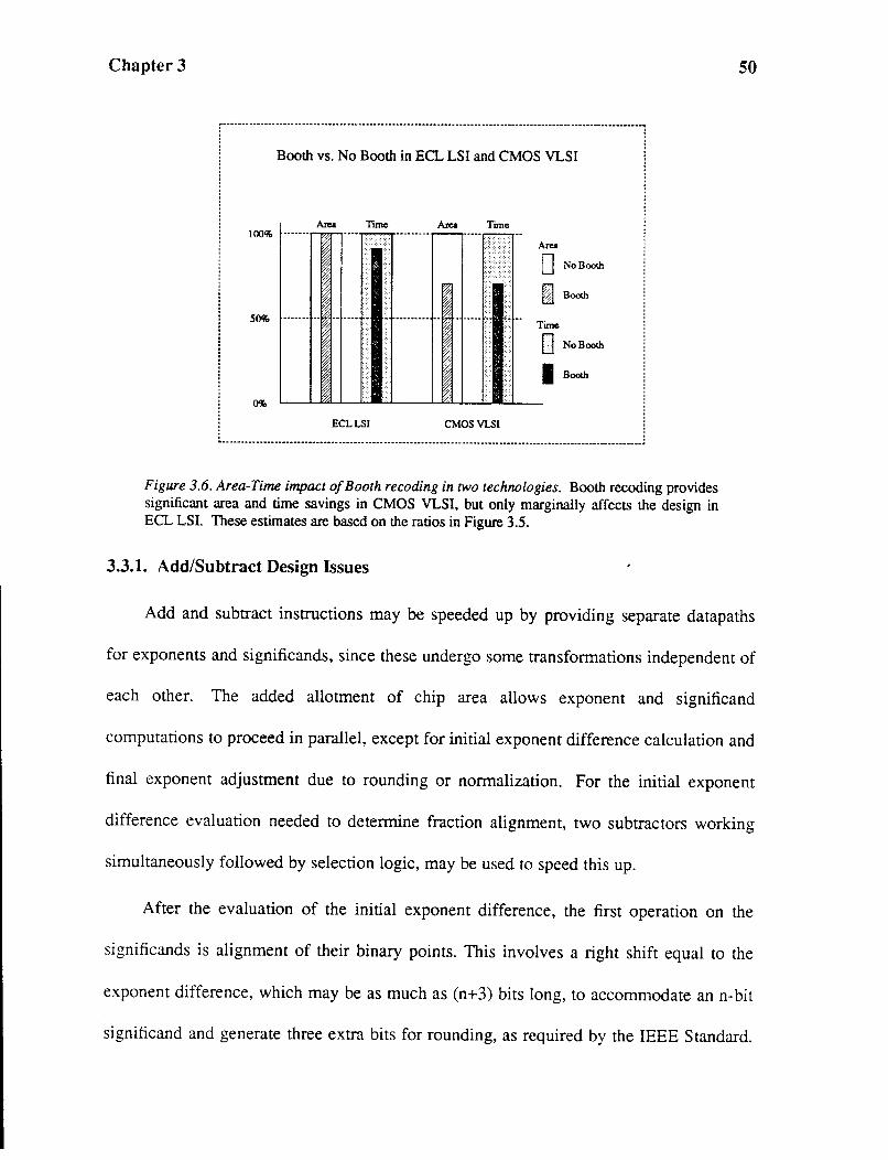
Chapter 3
, ...................................................................................................................................................................................................... __ ....... .. . . . ' . . . ' . . . ' Booth vs. No Booth in ECL LSI and CMOS VLSI
Area Tune Area Time
Area
D No Booth
~ Booth
Time
[] NoBooth
I sooth
ECLLSI CMOSVLSI
Figure 3.6. Area-Time impact of Booth recoding in two technologies. Booth recoding provides significant area and time savings in CMOS VLSI, but only marginally affects the design in ECL LSI. These estimates are based on the ratios in Figure 3.5.
3.3.1. Add/Subtract Design Issues
50
Add and subtract instructions may be speeded up by providing separate datapaths
for exponents and significands, since these undergo some transformations independent of
each other. The added allotment of chip area allows exponent and significand
computations to proceed in parallel, except for initial exponent difference calculation and
final exponent adjustment due to rounding or normalization. For the initial exponent
difference evaluation needed to determine fraction alignment, two subtractors working
simultaneously followed by selection logic, may be used to speed this up.
After the evaluation of the initial exponent difference, the first operation on the
significands is alignment of their binary points. This involves a right shift equal to the
exponent difference, which may be as much as (n+3) bits long, to accommodate ann-bit
significand and generate three extra bits for rounding, as required by the IEEE Standard.
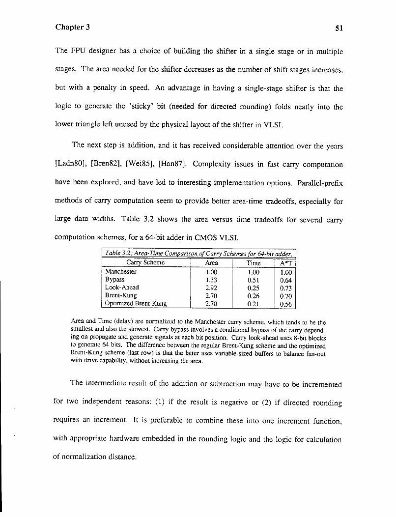
Chapter 3 51
The FPU designer has a choice of building the shifter in a single stage or in multiple
stages. The area needed for the shifter decreases as the number of shift stages increases,
but with a penalty in speed. An advantage in having a single-stage shifter is that the
logic to generate the 'sticky' bit (needed for directed rounding) folds neatly into the
lower triangle left unused by the physical layout of the shifter in VLSI.
The next step is addition, and it has received considerable attention over the years
[Ladn80], [Bren82], [Wei85], [Han87]. Complexity issues in fast carry computation
have been explored, and have led to interesting implementation options. Parallel-prefix
methods of carry computation seem to provide better area-time tradeoffs, especially for
large data widths. Table 3.2 shows the area versus time tradeoffs for several carry
computation schemes, for a 64-bit adder in CMOS VLSI.
Table 3.2: Area-Time Comparison of Carry Schemes for 64-bit adder. Carry Scheme Area Time A*T
Manchester 1.00 1.00 1.00 Bypass 1.33 0.51 0.64 Look-Ahead 2.92 0.25 0.73 Brent-Kung 2.70 0.26 0.70 Optimized Brent-Kung 2.70 0.21 0.56
Area and Time (delay) are normalized to the Manchester carry scheme, which tends to be the smallest and also the slowest. Carry bypass involves a conditional bypass of the carry depending on propagate and generate signals at each bit position. Carry look-ahead uses 8-bit blocks to generate 64 bits. The difference between the regular Brent-Kung scheme and the optimized Brent-Kung scheme (last row) is that the latter uses variable-sized buffers to balance fan-out with drive capability, without increasing the area.
The intermediate result of the addition or subtraction may have to be incremented
for two independent reasons: (1) if the result is negative or (2) if directed rounding
requires an increment. It is preferable to combine these into one increment function,
with appropriate hardware embedded in the rounding logic and the logic for calculation
of normalization distance.
Chapter 3 52
The final step, normalization, requires detection of the leading 1 in the intermediate
result, and a normalizing left shift to bring the leading 1 into the most significant bit.
Fast and efficient dynamic circuits can be used to detect the leading 1, and a bi
directional shifter can be used to combine the functions of alignment right shift and
normalizing left shift. Given that an initial long alignment shift implies that rounding
will be done and will preclude a final long normalizing left shift, independent paths for
rounding and normalizing can be provided in the fraction datapath to take advantage of
this fact, thus reducing total latency and yet nominally increasing area.
3.3.2. Multiply Design Issues
Since it is not feasible to build a 64 x 64 array multiplier as part of a single-chip
FPU with currently available technology, several iterative schemes need to be
considered. A 64 x 32 array requires 2 iterations to compute the full product, but takes
up about twice as much area as a 32 x 32 array, which requires 4 iterations. Even the
area of a 32 x 32 array just for the multiplier exceeds the current FPU area budget for
both multiply and divide.
Table 3.3 shows area versus time tradeoffs for different algorithms for
implementing a 64 x 64 multiply. Area and time are normalized to that chosen for
SPUR, which is an 8-bit recursive scheme.
A real implementation is constrained to work in a small range of Area-Time, as
shown in Figure 3.7. Available area defines the allowable region along the X-axis, while
performance criteria determine the acceptable range in the Y -axis. The acceptable region
is constantly changing with available technology, and design choices falling out of the

Chapter 3
Table 3.3: Area-Time Tradeoffs for 64 x 64 Multiply. Multiply Algorithm Area Time A*T
Serial (n=2) 0.1 8.0 0.8 Parallel (n=32) 1.9 0.7 1.3 Parallel (n=64) 4.0 0.5 2.0 Recursive (n=8) 1.0 1.0 1.0 Recursive (n=l6) 1.5 1.0 1.5
The area for the parallel scheme and the time for the serial scheme are too large, reducing the choice to recursive schemes. The higher-radix recursive scheme takes up more area, but does not run faster, contrary to expectation, because the delay time through the inner loop increases beyond a phase time, and it is no longer to run it at twice the external clock rate.
53
acceptable design space for one technology may very well become feasible in another
technology.
Time
0
0 Recursive (n=8)
2 3 4
Area
Figure 3.7. The Area-Time Design Space for Multiply. For current levels of integration, for example in 2 micron CMOS, a high-radix parallel scheme is too large for implementation, and so falls out of the acceptable design space, which is left unshaded.
The SPUR FPU multiplier is implemented in nme iterative steps, with each
iteration implementing a 64 bit by 8 bit multiplication. In each iteration, four overlapped
Chapter 3 54
triplets of multiplier bits (nine bits) are decoded by a modified Booth recoder. Four
multiplicand (MCD) multiples of magnitude +2M CD, + lMCD, -lMCD and -2MCD are
needed per iteration, along with 0. As mentioned earlier, the relative cost of a
multiplexor compared to that of an adder makes Booth recoding feasible in this CMOS
datapath. Also, separating the recoding from the carry-save-addition allows us to
evaluate them in separate time-slots in our pipelined implementation.
The four overlapped triplets of multiplier pairs generate the four multiples of the
multiplicand. They are added to the partial 'sum' and 'carry' terms of the previous
iteration, using an array of four carry-save-adders. Note that the four multiples of the
multiplicand are shifted left two bits with respect to each other, depending on the
significance of each multiplier triplet. The partial 'sum' and 'carry' are shifted right
eight bits and seven bits respectively, when looping them back to be the new inputs of
the CSA for the next iteration. Since there are negative as well as positive operands in
two's complement form, the multiplexers and CSA must be fully sign-extended to the
left (MSB) side. Further details are described in [Bose87].
A carry-look-ahead adder is necessary at the start of the multiply operation, to
produce the complement of the multiplicand. It is also necessary at the end to form the
final result by adding the partial product vectors. Since the fraction unit has such an
adder already, we share this module instead of duplicating it in the multiply/divide unit.
This increases the setup and completion times by 12%, but reduces the area of the
multiply/divide unit by 14%.
Chapter 3 55
3.3.3. Divide Design Issues
Restoring divide is the least area-expensive approach for radix-two division, but the
area increases exponentially with the number of bits generated per iteration. The same is
true of parallel-serial schemes. Multiplicative inverse schemes produce incorrectly
rounded quotients and inexact remainders, and later fix-ups can be area-expensive and
time-consuming. SRT division [Robe65], [Atki67] focuses attention on quotient digit
selection, and the remainder iteration does not require back-tracking. Higher radix SRT
division schemes are likely to provide significant gains in area and speed, as better ways
are found to provide compact quotient-selection logic, and concurrency between different
portions of the algorithm (like partial remainder formation and quotient selection) is
exploited.
Table 3.4 lists some characteristics of alternative schemes for division. In high-
radix SRT division, quotient selection becomes increasingly complex and time-
consuming, and becomes the dominant delay component in the pipelined internal loop,
slowing down the clock cycle time and hence the throughput. Quotient selection logic
complexity will probably limit the usefulness of the scheme for radices higher than 16.
Table 3.4: Characteristics of five Division schemes. Division Exponential Incorrectly Inexact Multiplier Quotient Scheme growth in cost rounded quotient remainder re_quired selection bottleneck
Restoring • Parallel-serial • Multiplicative Inverse • • • Prescaling • • SRT •
Multiplicative inverse produces incorrectly rounded quotients and inexact remainders, and makes conformance with the IEEE standard difficult Radix 16 SRT should become feasible with slightly denser technology.
Chapter 3 56
Figure 3.8 shows the area-time design space for divide. Prescaling schemes, which
currently require too much area, should become feasible as SRT schemes reach the
quotient selection bottleneck.
4
3
Time
2
1
0 2 3 4
Area
Figure 3.8. Area-Time Design Space for Divide. The unshaded area is the acceptable region of the area-time design space, where the boundaries are changing with technology. In 2 micron CMOS, radix-256 prescale dividers consume too much area and fall outside the feasible design space, for example.
The algorithm used in the SPUR FPU is based on radix-four, non-restoring division,
using estimates of the divisor and partial remainder. The radix-four quotient digits are
expressed using redundant representations of -2, -1, 0 + 1 and +2, and the partial
remainder is non-redundant. This redundancy in the quotient digits permits less
precision in comparing the divisor and partial remainder to select a quotient digit. The
precision required in inspecting the partial remainder and the divisor can be determined

Chapter 3 57
usmg P-D (Partial remainder-Divisor) plots. It can be shown that six bits of partial
remainder and four bits of divisor are needed to determine the next quotient digit [Frei61]
[Atki68].
The hardware loop for generating the next remainder and the next quotient estimate
contains an eight-bit carry-look-ahead-adder, which generates six most significant bits of
partial remainder. Together with these six bits, four most significant bits of the divisor
are sent to the quotient selection logic, which in tum generates three bits, representing
one of the five possible values of the quotient digit. Depending on the sign of the
quotient digit, it is channeled into one of two registers, one holding positive and the other
holding negative quotient estimates. These registe~s are shifted left two bits per iteration.
The quotient selection logic also controls a multiplexor, which decides the multiple of
the divisor to use for the next iteration.
3.4. Summary
In this chapter we have studied design alternatives for the three key aspects of
floating-point unit design: the interface, the quality of the arithmetic, and the algorithms
for the basic arithmetic functions.
The main contributors to a high performance interface are: • a decoupled control and execution architecture, which allow data transfers to proceed while FPU functions are performed; • on-chip FPU register file and a wide data path between the memory and FPU, which minimize data transfer overhead;
• an intelligent interface control unit allows FPU instruction decoding and execution in parallel with CPU instruction decoding and execution, allowing maximum concurrency; and

Chapter 3
• implicit and explicit synchronization mechanisms, providing the programmer complete control and flexibility.
58
The IEEE Floating-point Standard 754 is emerging as the industry standard for
assuring quality and consistency of floating-point arithmetic, with such features as
correct and unbiased rounding, gradual underflow, and exception detection and handling.
The implications of hardware support for the IEEE standard were analyzed in this
chapter, and the basis for partitioning tasks between hardware and software were
explored. It is found that it is possible to delegate the evaluation of special functions and
exception handling to software, and implement the rest in hardware, while still retaining
high performance. Lee [Lee86] completed the FPU functional simulator and verified it
against the IEEE Test Suite.
In the final section of this chapter, the hardware costs for implementing the basic
arithmetic functions are studied. Area and time costs for different schemes are
compared, and the suitability of different algorithms determined. For a floating-point
unit implemented on a single chip in 2j.l. CMOS technology, it is found that high-radix
iterative techniques work well for multiply, and significant hardware sharing occurs if
implemented together with iterative SRT divide.
The next three chapters discuss the details of the microarchitecture, logic, circuit,
and layout design issues in the implementation of datapath and control functions.

Chapter 3 59
3.5. References
[Atki67] D. E. Atkins, The Theory and Implementation of SRT Division, Report No. 230, Dept. of Computer Science, Unviersity of Illinois (June, 1967).
[Atki68] D. E. Atkins, Higher-Radix Division Using Estimates of the Divisor and Partial Remainders, IEEE Trans. Computers, Vol. C-17, No. 10(0ctober 1968), pp. 925-934.
[Bose87] B. K. Bose, L. Pei, C. Lee and D. A. Patterson, Fast Multiply and Divide for a VLSI Floating-Point Unit, Proc. Eighth Int' l. Symposium on Computer Arithmetic(May 1987), pp. 87-94.
[Bren82] R. P. Brent and H. T. Kung, A Regular Layout for Parallel Adders, IEEE Trans. on Computers, Vol. C-31, No. J(March 1982), pp. 260-264.
[Cody84] W. J. Cody, J. T. Coonen, D. M. Gay, K. Hansen, D. Hough, W. Kahan, R. Karpinski, J. Palmer, F. N. Ris and D.Stevenson, A Proposed Radix- and Word-length-independent Standard for Floating-point Arithmetic, IEEE Micro, Vol. 4, No.4 (August 1984).
[Frei61] C. V. Freiman, Statistical Analysis of Certain Binary Division Algorithms, ProcJRE, Vol. 49(January 1961), pp. 91-103.
[Han87] T. Han and D. A. Carlson, Fast Area-Efficient VLSI Adders, Proc. Eighth IEEE Int' /.Symposium on Computer Arithmetic(May 1987), pp. 87-94.
[Hans86] P. M. Hansen and S. I. Kong, SPUR Coprocessor Interface Description, Computer Science Division (EECS) Report No. UCB/CSD 87/308, University of California, Berkeley (October 1986).
[Hans88] P. M. Hansen, Coprocessor Architectures for VLSI, PhD. Dissertation(November, 1988).
[Kane85] R. Kane, personal communication, Intel Applications Engineering, (April 1985).
[Ladn80] R. E. Ladner and M. J. Fischer, Parallel Prefix Computation, JACM, vol. 27, No. 4(0ctober 1980), pp. 831-838.
[Lee86] C. Lee, Unpublished Document: Micro-architecture of the SPUR Floatingpoint Unit, Unpublished Report, University of California, Berkeley, Computer Science Division, Berkeley, CA (March 17, 1986).
[Lee89] C. Lee, Multi-Step Variable Rounding for the IEEE Floating-Point Standard, accepted/or publication in IEEE Transactions on Computers(l989).
[Leun86] B. Leung and Y. M. Lin, Statistics on Floating-point Arithmetic, CS 252 Class Project(May 1986).
[Prio84] J. Prioste and A. Bass, Motorola MCA2500ECL Macrocell Array Design Manual (1984).
[Robe65] J. E. Robertson, Methods of Selection of Quotient Digits during Digital Division, File No. 663, University of Illinois, Urbana (June 1965).
[Sarr85] C. Sarreno, personal communication, Applications Engineering, Motorola Advanced Microprocessor Division, (April 1985).
Chapter 3 60
[Wei85] B. W. Y. Wei, C. Thompson andY. Chen, Time-Optimal Design of a CMOS
Adder, Technical Report No. UCB/CSD 86/252, U.C. Berkeley (August, 1985).
4 Add/Subtract Datapath Design Considerations
61
This chapter and the next present datapath design considerations for performing
data manipulations on memory and arithmetic operations. While this chapter
concentrates on the components needed for addition and subtraction, Chapter 5 focuses
on multiplication and division. Design examples will be drawn from the SPUR FPU,
which implements extended precision arithmetic using hard-wired control. An overview
of a floating-point unit datapath will be followed by design details of the different
components and their key building blocks. Area-time tradeoffs that went into the micro
architecture, logic, circuit, and layout design decisions will also be discussed. Of special
interest are the unique design implications of the very wide data widths in floating-point
Chapter 4 62
unit datapaths.
4.1. Implementation Considerations
Using process yield curves, an estimate for the size of a floating-point unit in 2
micron CMOS is lOmm x lOmm. Accounting for pads and other peripheral circuits, this
leaves about 9mm on a side for circuits. Allowing 25% area for control and routing, this
leaves 60 square mm for the exponent and fraction datapaths. As discussed in Chapter 2,
operation frequencies can serve as a guideline for choosing the most appropriate
algorithm and for budgeting hardware.
The maximum width of the fraction datapath is 75 bits (for example, the partial
product vectors for multiply). Delay in control signals that run the entire length of the
datapath has a large impact in the delay in and between modules in the datapath. If there
is any appreciable resistance in these control lines, the RC delay can become a significant
fraction of module delay, leading to slower computation rates and large clock non
overlap times to protect against clock skew. We chose a process with two layers of metal,
using one for control and the orthogonal data signals in the other metal layer, thus
virtually eliminating any resistive delay. To minimize clock skew, we scale the drivers of
the control lines to match the capacitances they have to drive, so that control delay is
held between very tight tolerances for the entire width of the datapath.
To allow for a mix of static and dynamic design styles, we chose a four-phase
clocking scheme, also used in the other chips in the SPUR system. A four-phase clock
allows two register file accesses per cycle -- one phase going for read and one for write.
The two intermediate phases between read and write are used for precharging the
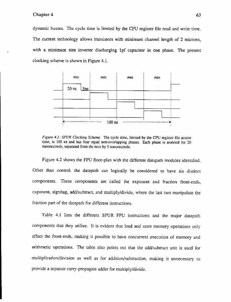
Chapter 4 63
dynamic busses. The cycle time is limited by the CPU register file read and write time.
The current technology allows transistors with minimum channel length of 2 microns,
with a minimum size inverter discharging 1 pf capacitor in one phase. The present
clocking scheme is shown in Figure 4.1.
PIDl
_j 20 ns
PID4
~~5~ns+l------+-----~------~~ PID2 PID3
r··------------------------------------ 100 ns -----------------------------------------------~
Figure 4.1: SPUR Clocking Scheme. The cycle time, limited by the CPU register file access time, is 100 ns and has four equal non-overlapping phases. Each phase is asserted for 20 nanoseconds, separated from the next by 5 nanoseconds.
Figure 4.2 shows the FPU floor-plan with the different datapath modules identified.
Other than control, the datapath can logically be considered to have six distinct
components. These components are called the exponent and fraction front-ends,
exponent, sign/tag, add/subtract, and multiply/divide, where the last two manipulate the
fraction part of the datapath for different instructions.
Table 4.1 lists the different SPUR FPU instructions and the major datapath
components that they utilize. It is evident that load and store memory operations only
affect the front-ends, making it possible to have concurrent execution of memory and
arithmetic operations. The table also points out that the add/subtract unit is used for
multiplication/division as well as for addition/subtraction, making it unnecessary to
provide a separate carry-propagate adder for multiply/divide.
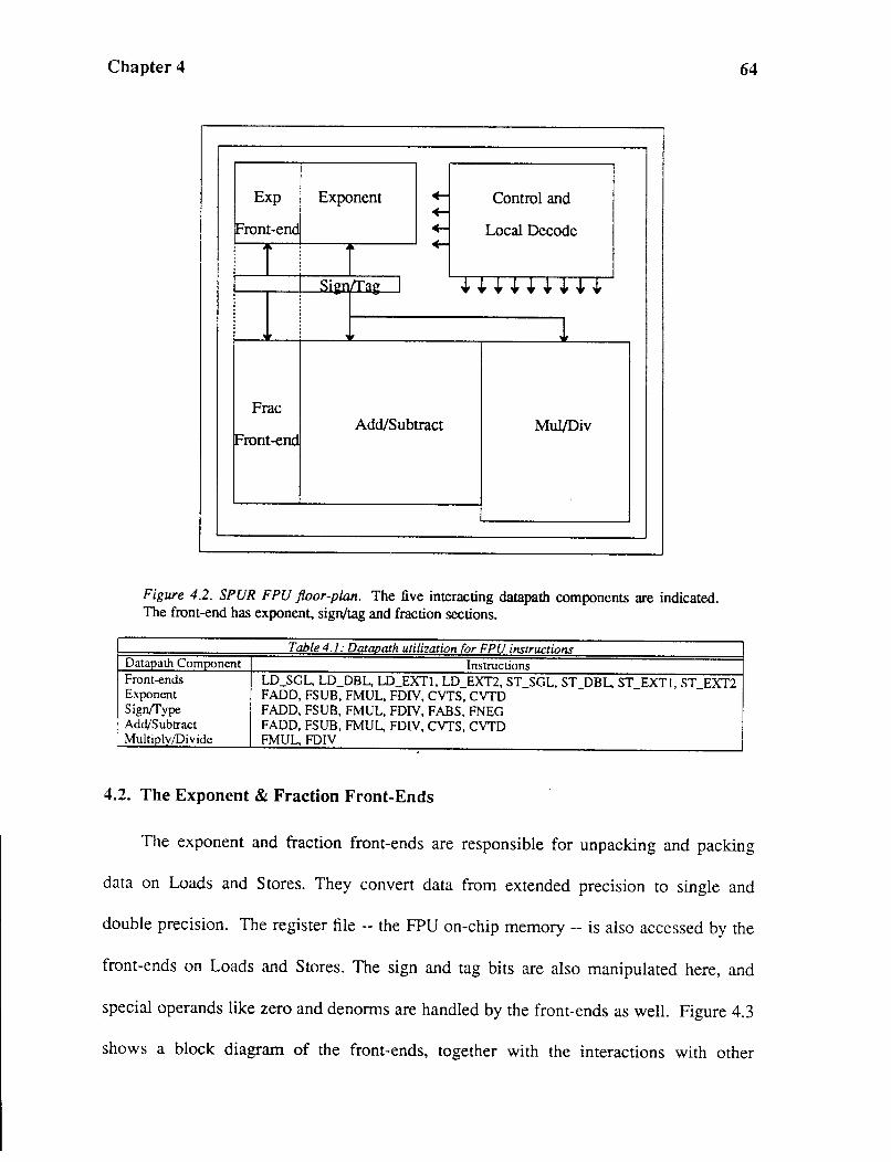
Chapter 4
Exp Exponent Control and
Local Decode
Frac Add/Subtract Mul/Div
ront-en
Figure 4.2. SPUR FPU floor-plan. The five interacting datapath components are indicated. The front-end has exponent, sign/tag and fraction sections.
Table 4.1: DataDath utilization for FPU instructions Datapath Component Instructions
64
Front-ends LD_SGL, LD_DBL, LD_EXTl, LD_EXT2, ST_SGL, ST_DBL, ST_EXTl. ST_EXT2 Exponent FADD, FSUB, FMUL, FDIV, CVTS, CVTD Sign(fype FADD, FSUB, FMUL, FDIV, FABS, FNEG Add/Subtract FADD, FSUB, FMUL, FDIV, CVTS, CVTD Multiply/Divide FMUL, FDIV
4.2. The Exponent & Fraction Front-Ends
The exponent and fraction front-ends are responsible for unpacking and packing
data on Loads and Stores. They convert data from extended precision to single and
double precision. The register file -- the FPU on-chip memory -- is also accessed by the
front-ends on Loads and Stores. The sign and tag bits are also manipulated here, and
special operands like zero and denorms are handled by the front-ends as well. Figure 4.3
shows a block diagram of the front-ends, together with the interactions with other

Chapter 4
datapath components.
Fraction Exponent
PADS -----,
i ! r-· I j
.----j i -----------~--------, + :.sl9~lilch:jl3lc;.-----~ i
I i [[
------- ___________ _i _______ , i :.l=P~~~~:I.DYj.---~---~ !
! ~-----l
<63>
frac-regbusA Type
i r· _______________ j_~ ~ .. !;.3,p-J...ili~:l.ilt'<b . ._.J
'------. ... E'"·------J
exp-shifter
r-------------.. ---------------~-l
L. .lJllilch:jlQn:~lll2."lti~
!
<0> <16>
exp-regbusA
Figure 4.3. The exponent and fraction front-ends. All components of the front-ends, except the register file and sign and tag logic, are shown here. The solid lines and solid-lined logic boxes show information flow on a Load, moving from the top of this page towards the bottom: beginning with the pads, through the master and slave load latches and shifter, and to the register bus. The dashed lines and the dash-lined logic boxes show information flow on a Store, moving from the bottom of the page towards the top: beginning with the register bus, through latches and shifter, and back to the pads. There are two lines that are exceptions, though -- the solid line going up takes exponent bits from the input into the exponent front-end on a Load; and the dashed line going down brings the output of the exponent front-end back to the fraction front-end for a Store.
65

Chapter 4 66
4.2.1. Unpacking and Packing Data
The FPU converts or unpacks all incoming operands into a common internal format.
For extended precision, this involves extraction of the appropriate exponent, sign, and tag
fields for LD __ EXTl, with the fraction unaltered for LD_EXT2. For single and double
precision, the exponent has to be moved to the least significant position of the stored
exponent using a right shift. The fraction, on the other hand, is shifted left so that it is
positioned just after the binary point.
Corresponding reverse-mapping or packing has to be done when storing operands
back to off-chip memory. The exponent, sign and tag fields need to be brought together
for ST_EXTl, or extended precision store. And for single and double precision, the
exponent now gets appropriately left-shifted and the fraction right-shifted. Figure 4.4
shows the different data formats and the relative positions of the different fields.
<0> <7:0> <22:0>
SINGLE lsi E I F
<0> <10:0> <51:0>
DOUBLE lsi E F
<0> <16:0> <4:0> <31:0>
EXT! lsi E I ttl T I Ill
<63:0>
EXT2 F
<16:0> <0> <4:0> <63:0>
E 10~ F
COMMON INTERNAL FORMAT
Figure 4.4. Floating-point data formats. The sizes and positions of the different data fields as stored in memory are indicated with respect to the common internal format, which is the way operands are stored in the internal registers.

Chapter 4 67
4.2.2. Handling Special Operands
After computation, the FPU can only produce two types of result operands: a
normalized number or zero. On a Load, however, an operand could have one of three
other types as well: denorm, infinity or NaN. It is essential that the incoming operand
type be determined -- that is, the appropriate data type tags be set -- before it is stored in
a register.
Four pieces of information determine the three-bit encoding for the operand data
type, and Table 4.2 shows this encoding. If all bits to the right of the binary point are
zero, f-al/0 is set. e-al/0 or e-al/1 is set when all exponent bits are 0 or 1, respectively. f-
2msb indicates the setting of the second bit to the right of the binary point.
Table 4.2: Encoding for data type tags bit<2> bit<1> bit<O>
Data Type e-alll e-allO f-2msb f-allO
0 0 - 0 nonnalized 0 0 - 1 nonnalized, power of 2 0 1 - 0 denonn 0 1 - 1 zero 1 - 0 0 quiet NaN 1 - 0 1 infinity 1 - 1 0 signaling NaN 1 - 1 1 cannot occur
Don't care values in e-al/0 and f-2msb are indicated with dashes. In practice, only three bits are needed to specify the seven operand types. The reduction of four variables to three bits is made possible by having e-alll act as the control signal to a multiplexor which selects between e-al/0 and f-2msb. The table spells out the encoding in tenns of four variables to attach a clearer physical meaning to the three tag bits, and the conversion can be visualized by reading each row as a three-bit encoding by merging the second and third columns.
The combination 000 is the value set by the hardware as the result of an arithmetic
operation. The combination 111 cannot occur, since both f-2msb and f-allO cannot be 1
simultaneously. The encoding 001 identifies operands which are exact powers of two,
and could conceivably be used by software to provide a fast scaling operation, often used

Chapter 4 68
in equilibration -- a technique involving multiplying some matrix elements by multiples
of two.
4.2.3. Conversion to Single and Double Precision
The instruction set is designed to allow maximum parallelism between memory
operations and arithmetic computations within the fpu. Thus, Loads and Stores cannot
cause traps or exceptions, but since intermediate results are in extended precision,
explicit instructions for conversion to single and double precision need to be executed
before storing a single or double precision operand.
If the result of a conversion is zero, the exponent gets the 8-bit or 11-bit
representation for zero in single and double precision, respectively. Otherwise, the result
exponent is the sum of the original exponent, the normalizing distance and 40 for
conversion to single precision (CVTS) or 11 for conversion to double precision (CVTD).
Correspondingly, the fraction first gets an alignment right shift of 40 or 11, followed by
rounding and normalization. If an operand is found to be a NaN or infinity during
conversion, an operand exception is signaled.
4.2.4. The Register File
All incoming operands and computed results are stored on-chip in the register file in
the common internal format. The register file is 87 bits wide, with 17 bits for exponent,
one for sign, five for tags, and 64 for fraction. The FPU has 16 externally addressable
registers, with RO hard-wired to zero and R15 reserved for control and status information.

Chapter 4 69
The register file has four ports, two for input and two for output. Thus at the
beginning of a two-operand arithmetic instruction, both operands can be read at the same
time. Recall that the FPU allows memory operations to overlap with arithmetic
operations, so a register write from a Load and a result register write can occur
simultaneously. Software convention is used to ensure that the two writes are to different
registers to ensure data consistency.
Reg-bus A
~rite*
Reg-bus B
Figure 45. FPU Register Cell. The cell allows simultaneous reads and writes to and from busses A and B. Results of Loads and operands for Stores are sent on bus A while results of arithmetic instructions are written back on bus B. A* implies the complement of a signal, and so Write* implies Read (together with non-overlap times). Inverter #2 is designed larger than inverter #1 to minimize delay time for register read, when it has to drive the relatively large register bus capacitance.
Figure 4.5 shows the circuit for the register cell. It contains nine active devices,
where four are transmission gates providing read and write access to the two data busses
A and B. The rest of the cell is a pseudo-static latch. During read, the latch feedback
path is closed, while for write, it is open. Thus there is never any fight between input data
and what is in the cell, making a more process-insensitive cell design easier.

Chapter 4 70
Both data busses are precharged to increase speed and reduce area and power of the
bus drivers. Since the high level at X (in Figure 4.5) is degraded by the access
transmission gates, the ratio of inverter 1 is skewed, with a stronger pull-down device
than usual. Inverter 2 is larger than inverter 1 to provide greater drive to allow for fast
discharge of the data busses.
Rc&ift:r Spec:ifior Bi'" EN EN
3• 2 2• 1 1• o o• WrA RdA pbiEV phiEV•
Figure 4.6. The Register File Decoder. Two sets of decoders are necessary to read and write . both busses. The design is pseudo-static, with pullup by P channel transistors with gates tied
to ground.
The timing of the register busses and register cell directly affect the timing of the
register file decoder. A new instruction is received at the end of phi3, and so the decoder
input latch changes in phi4. Thus it is not possible to use a dynamic decoder during phi4,
a phase ahead of the actual register read. Hence a pseudo-static decode scheme is
chosen, shown in Figure 4.6, so that the decode can complete in phi4 and still have all of

Chapter 4 71
phil for the register read itself. Another design option was to stay with a dynamic
decoder, but do the decode and read all in phi 1. This was rejected because the register
read time together with the data transfer to the main data busses and latching the data in
the data latches leaves little time margin for the decoder. Phi4 is used for effectively this
way, albeit at the expense of a small amount of DC power, and there is more design
margin for the read.
Table 4.3: Re!:ister File Timing Component Delay
Decoder 8.8 ns Reg Cell Read 4.8 ns Reg Cell Write 4.5 ns RegBus to MainBus 4.1 ns
Table 4.3 summarizes the delays in each of the circuit blocks of the register file.
The main data busses are static, unlike the internal register busses, and so the register
data is buffered by tri-state inverting buffers before they are latched. Since the main
busses have high capacitance, this extra level of buffering allows high cell speed without
needing very large device sizes in the register cell itself.
4.3. The Exponent Datapath
The exponent is stored internally as a 17 -bit number, in two's complement - 1
format. Even though extended precision requires a 15-bit exponent, two extra bits are
kept for handling gradual underflow. One bit allows the FPU to represent denorms in
normalized form, and the other bit allows evaluation of the product of two denorms.
Figure 4. 7 shows the floorplan of the exponent datapath. The three main
components are the difference unit, the normalization adjustment, and the
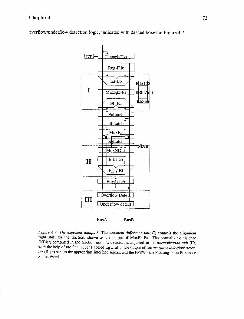
Chapter 4
overflow/underflow detection logic, indicated with dashed boxes in Figure 4.7.
I
j III L•••4•••••••••••••• ••••••••••••••••••••••••• ••••••••••••••••••_.
BusA BusB
Figure 4.7. The exponent datapath. The exponent difference unit (I) controls the alignment right shift for the fraction, shown as the output of MuxEb-Ea. The normalizing distance (NDist) computed in the fraction unit 1 's detector, is adjusted in the normalization unit (II), with the help of the final adder (labeled Eg ± El). The output of the overflow/underflow detector (III) is sent to the appropriate interface signals and the FPSW- the Floating-point Processor Status Word.
72

Chapter 4 73
4.3.1. The Exponent Difference Unit
Determining the difference between the exponents of the two operands is the first
step in floating-point addition and subtraction. To achieve high speed for this operation,
the FPU sacrifices some extra area to provide two subtractors that compute (A-B) and
(B-A) concurrently. The positive difference is selected, and the seven lower-order bits
are sent to the fraction shifter decoder so that the fraction with the larger exponent is
right-shifted appropriately. The remaining bits of the difference are ORed to indicate
whether the exponent difference is greater than 128, in which case the fraction with the
larger exponent is given the maximum shift. A signal is also sent to the fraction unit
indicating which exponent was greater, and it is used to control a mux that selects the
fraction to be right-shifted.
4.3.1.1. A Fast Adder/Subtractor
A good deal has been published on addition and subtraction [Han87] in the past few
years, especially about carry propagation, which is usually the bottleneck for numbers
more than a few bits wide. As mentioned in Chapter 3, studies in VLSI complexity
issues in fast carry computation have led to many interesting implementation options,
and parallel-prefix methods of carry computation seem to provide better area-time
tradeoffs, especially for large data widths.
The FPU uses a variation of parallel-prefix computation for carry evaluation in most
of its wide adders, including the 17 -bit dual subtractors and normalization adjusting
adder, and the 66-bit adder and 67 -bit incrementer in the fraction unit. A prefix
computation is one in which the output depends only on the lower-order inputs and not

Chapter 4 74
on the higher-order inputs [Ladn80]. Binary addition can be transformed into a prefix
computation by introducing an associative operator ( o) as follows:
(4.1)
(4.2)
c; =G; fori= 1,2, · · · ,n (4.3)
where
{
(giN 1, piNt) (G; ,P;) =
(giN; ,p/N;)o(Gi-t, Pi-1) ifn~i>l
ifi=l (4.4)
and the operator o is defined as:
(4.5)
(4.6)
Note that o is not commutative -- its left argument (g1 , p1) is treated differently from its
right argument (gr ,pr). After the carry bit c; is computed, the sum bits; is given by:
S; = plN;OC;_1 fori= 2, · · ·, n (4.7)
and
Sl =pl (4.8)
Given that (o) is associative, choose a m such that i~m>l and rewrite (G;,1 ,P;,1) as
follows:
(4.9)
where
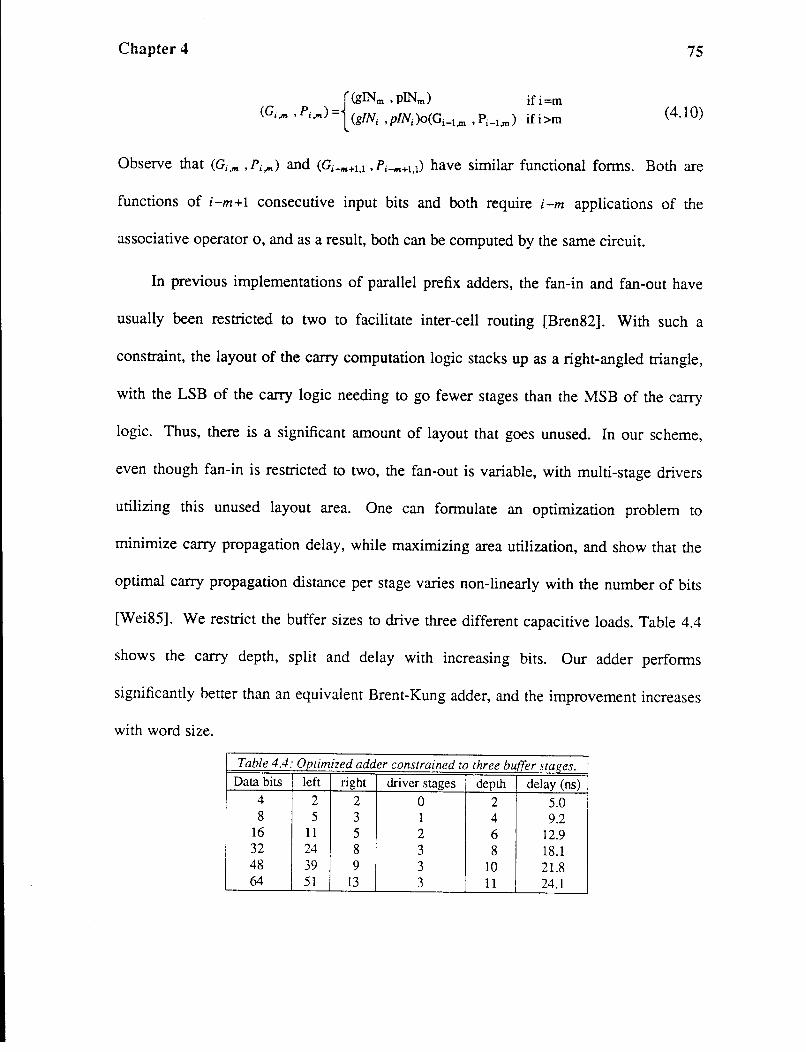
Chapter 4 75
(4.10)
Observe that (Gi,. ,P,,.) and (Gi-m+t.l ,P,_,.+1,1) have similar functional forms. Both are
functions of i-m+1 consecutive input bits and both require i-m applications of the
associative operator o, and as a result, both can be computed by the same circuit.
In previous implementations of parallel prefix adders, the fan-in and fan-out have
usually been restricted to two to facilitate inter-cell routing [Bren82]. With such a
constraint, the layout of the carry computation logic stacks up as a right-angled triangle,
with the LSB of the carry logic needing to go fewer stages than the MSB of the carry
logic. Thus, there is a significant amount of layout that goes unused. In our scheme,
even though fan-in is restricted to two, the fan-out is variable, with multi-stage drivers
utilizing this unused layout area. One can formulate an optimization problem to
minimize carry propagation delay, while maximizing area utilization, and show that the
optimal carry propagation distance per stage varies non-linearly with the number of bits
[Wei85]. We restrict the buffer sizes to drive three different capacitive loads. Table 4.4
shows the carry depth, split and delay with increasing bits. Our adder performs
significantly better than an equivalent Brent-Kung adder, and the improvement increases
with word size.
Table 4.4: Optimized adder constrained to three buffer stages. Data bits left right driver stages depth delay (ns)
4 2 2 0 2 5.0 8 5 3 1 4 9.2
16 11 5 2 6 12.9 32 24 8 3 8 18.1 48 39 9 3 10 21.8 64 51 13 3 11 24.1

Chapter 4 76
This design is used for the exponent and fraction adders, and is implemented in
fully static CMOS. Even though the cells are larger than their dynamic counterparts, the
non-overlap time between phases gets utilized for computation. The fraction adder is
also shared by several instructions at different cycles and phases, and a dynamic design
would increase the control complexity needed for precharge and evaluate signals.
Figure 4.8 shows the main components of the adder. The pre-condition logic transforms
the inputs into propagate and generate form according to equation 4.5, while the sum
logic implements equation 4.7. The carry generator implements the recursive relation
4.10, optimized for minimum delay.
a,..b,.
fast carry
generator
pre-condition sum
Figure 4.8. Floor-plan for optimized adder. The output s 1 depends solely on inputs a 1 and b 1;
Caut does not require a final exclusive-or, as is Lhe case wilh conventional carry computation.
Figure 4.9 shows the components of the fast carry generator, which consists of three
types of cells: black, white, and driver. The cells are designed with embedded routing
and matching cell pitches so that they can be abutted in any order. This proved very
helpful, since simple CAD tools were then written to create carry generators for any
desired data width. The white and driver cells are naturally inverting, but the black cells

Chapter 4 77
are not; thus, two versions of black cells were created, one generating complementary
output for true input, and the other generating true output for complimentary input,
saving extra delays due to signal inversion.
Pr
PI
gout = gl + P1 · g,
Pout =P1. Pr
Black Cell
Pr PI
Pout
White Cell Driver Cell
Figure 4.9. Basic cell types for fast carry generator. White cells and driver cells produce an inversion from input to output; two types of black cells are used to provide the necessary·logical inversion.
A 5-bit example in Figure 4.10 illustrates the optimization in the carry generator.
The optimal split for five inputs is three on the top and two on the bottom in the first
stage. The two on the bottom are reduced at the next stage into one and one, while the
three on the top are reduced to one on the top and two on the bottom. In the third stage,
these two on the bottom are reduced to one and one.
It is not easy to determine the worst-case path of the carry generator by inspection,
since the optimizer tries to balance delay through black cells and through multi-stage
drivers. Timing simulation using Crystal [Oust83] was done to determine worst-case
delays in the different adders. For the 66-bit adder in the fraction datapath, the pre-
condition and sum logic accounted for 9 ns, and the fast carry generator required another
25 ns for a total adder delay of 34 ns.
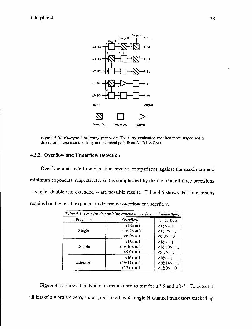
Chapter 4
out
A4,B4
A3,B3
A2,B2
Al,Bl
AO,BO
Inputs Outputs
~ D C> Black Cell White Cell Driver
Figure 4.10. Example 5-bit carry generator. The carry evaluation requires three stages and a driver helps decrease the delay in the critical path from Al,B 1 to Cout
4.3.2. Overflow and Underflow Detection
78
Overflow and underflow detection involve comparisons against the maximum and
minimum exponents, respectively, and is complicated by the fact that all three precisions
-- single, double and extended -- are possible results. Table 4.5 shows the comparisons
required on the result exponent to determine overflow or underflow.
Table 45: Tests for determinin~? exponent overflow and underflow. Precision Overflow Underflow
<16> * 1 <16> = 1 Single <16:7> '1:0 <16:7> = 1
<6:0> = 1 <6:0>= 0 <16> 'I= I <16> = 1
Double <16:10> * 0 <16:10> = 1 <9:0> = 1 <9:0> = 0
<16> * 1 <16>= 1 Extended <16:14> * 0 <16:14> = 1
<13:0> = 1 <13:0> = 0
Figure 4.11 shows the dynamic circuits used to test for all-0 and all-1. To detect if
all bits of a word are zero, a nor gate is used, with single N-channel transistors stacked up
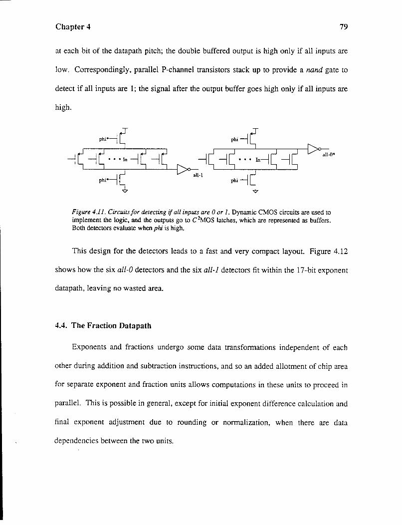
Chapter 4 79
at each bit of the datapath pitch; the double buffered output is high only if all inputs are
low. Correspondingly, parallel P-channel transistors stack up to provide a nand gate to
detect if all inputs are 1; the signal after the output buffer goes high only if all inputs are
high.
Figure 4.11. Circuits for detecting if all inputs are 0 or 1. Dynamic CMOS circuits are used to implement the logic, and the outputs go to C 2MOS latches, which are represented as buffers. Both detectors evaluate when phi is high.
This design for the detectors leads to a fast and very compact layout. Figure 4.12
shows how the six all-0 detectors and the six ali-I detectors fit within the 17-bit exponent
datapath, leaving no wasted area.
4.4. The Fraction Datapath
Exponents and fractions undergo some data transformations independent of each
other during addition and subtraction instructions, and so an added allotment of chip area
for separate exponent and fraction units allows computations in these units to proceed in
parallel. This is possible in general, except for initial exponent difference calculation and
final exponent adjustment due to rounding or normalization, when there are data
dependencies between the two units.
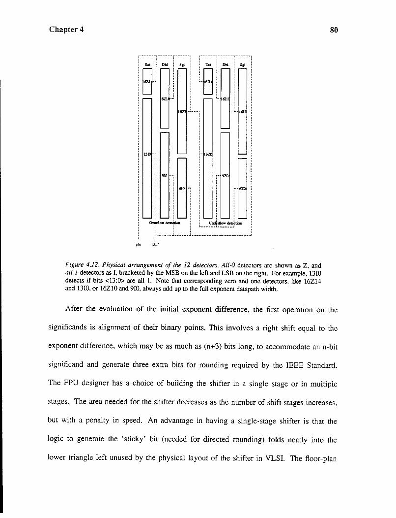
Chapter 4
r ~· ··-·· ··:·---·· ···1· ------- ··:
i OJ .. I ··1 :0 j i i 6Zl -~ i 1 i
,. ....... ----- ....................... ,. .................. .. . ' ' . !&t!obl!sc~!
l-8 i i l L 611 l J
: ······] '· 1617
131 ~- 13
910 "1:::, 610 ••
1. 6ZD
9ZD
or-~ ~ ..... ~~~~-~lim ' ' ' ~- --- ... --- ~--- -- ..................................... - .. - ........... - ·----------.. -- .. .!
phi phi"
Figure 4.12. Physical arrangement of the 12 detectors. All-0 detectors are shown as Z, and all-1 detectors as I, bracketed by the MSB on the left and LSB on the right. For example, 1310 detects if bits <13:0> are all 1. Note that corresponding zero and one detectors, like 16Zl4 and 1310, or 16Zl0 and 910, always add up to the full exponent datapath width.
80
After the evaluation of the initial exponent difference, the first operation on the
significands is alignment of their binary points. This involves a right shift equal to the
exponent difference, which may be as much as (n+3) bits long, to accommodate ann-bit
significand and generate three extra bits for rounding required by the IEEE Standard.
The FPU designer has a choice of building the shifter in a single stage or in multiple
stages. The area needed for the shifter decreases as the number of shift stages increases,
but with a penalty in speed. An advantage in having a single-stage shifter is that the
logic to generate the 'sticky' bit (needed for directed rounding) folds neatly into the
· lower triangle left unused by the physical layout of the shifter in VLSI. The floor-plan

Chapter 4
for the fraction datapath for addition and subtraction is shown in Figure 4.13.
I
I I
I
I
I -01 01
I
l I
I
u1 01
"" ut w-u1 I ,_ l Tst
IRIPLI I--
I
I
l
l
<63:0>
Dul/04tU,_.c.....,. I
Roplcd'ilo
BUI Drivcm
AlAd!
-=:-1 DIAd>
1 MuxPO
l MullA
OpALir<
LSbiliOIIIl. <dl ,___, '--!--a.t.l3llill<o
r-*--1. ~iJIOull.alch
~ I I LSbilllcLoj.:b
1---1 1 Muxll
l OpBIAdl
I
B +/-A
j_ lnlLadl
~ 1 Campi em.,.
l RJPL!Sbift
1 ISJbitlne
I ln<:Oull.alcl!
~ 1 hDel«tar
BUlB
<4:0>
IE] I
...-I I RT&DT I
I I I RT&DT I
...-I
l I
I <2,0>
J GIU
I ~
J ~
I ~
~--- 1 I I I
I
I!opoaoot I
a.. I I
L--
/II j GRS
I
J
Jl J
I
BuoA
~
~R --1
OUDd I PLA I I
4hU.Inc h_ ~
GRS
Figure 4.13. The fraction datapath for addition and subtraction. The data path is 67 bits wide, to accommodate 64-bit extended precision numbers, together with 3 bits (Guard, Round and Sticky) that provide correct, unbiased IEEE-style rounding. In addition to the register file, key components in the datapath include the shifter, adder and incrementer, and a leading 1 's detector. These are highlighted in the figure.
81
The next step involves an addition or subtraction between the two fractions, one of
which is 67 bits wide; this leads to a 67-bit intermediate result in two's complement
form. The intermediate result of the addition may have to be incremented for two

Chapter 4 82
independent reasons: (1) if it is negative, and/or (2) if directed rounding requires an
increment. It is possible to combine these into one increment function, with appropriate
hardware embedded in the rounding logic and the logic for calculation of normalization
distance, thus avoiding another incrementer delay.
The final step, normalization, requires detection of the leading 1 in the intermediate
result, and a normalizing left shift to bring the leading 1 into the most significant bit.
Fast and efficient dynamic circuits can be used to detect the leading 1, and a bi-.
directional shifter can be used to combine the functions of alignment right shift and
normalizing left shift. Given that an initial long alignment shift implies that rounding
will be done and will preclude a final long normalizing left shift, independent paths for
rounding and normalizing can be provided in the fraction datapath to take advantage of
this fact, thus reducing total latency and yet nominally increasing area.
4.4.1. The Shifter
The bi-directional shifter is used for alignment and normalization. For right shift,
the incoming word is 64-bits wide, and the shift ranges from 0 to 66, providing the Guard
(G), Round (R), and Sticky (S) bits for IEEE-style rounding. For left shift, the input
width is 67 bits, the output is 64 bits, and the shift range is 0 to 64. The shifter decoder
selects between the exponent difference and the normalizing distance for right and left
shift, respectively. If the exponent difference is greater than 66, the input is still shifted
right by the maximum shift distance. The shifter is designed to decode, shift, and
evaluate the Sticky bit in one phase time, and so the shifter is implemented as a single
stage to meet these stringent speed requirements. The three main components of the
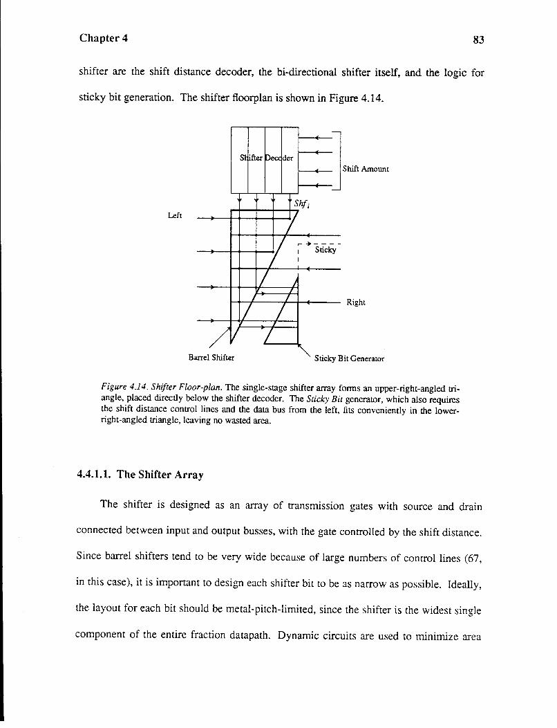
Chapter 4 83
shifter are the shift distance decoder, the bi-directional shifter itself, and the logic for
sticky bit generation. The shifter floorplan is shown in Figure 4.14.
-
s~ ifter pecc der Shift Amount
-i Shfi
Left I J
y r-+----I Sticky I
I I , I I
I I Right
, /V I
Barrel Shifter Sucky Bit Generator
Figure 4.14. Shifter Floor-plan. The single-stage shifter array forms an upper-right-angled triangle, placed directly below the shifter decoder. The Sticky Bit generator, which also requires the shift distance control lines and the data bus from the left, fits conveniently in the lowerright-angled triangle, leaving no wasted area.
4.4.1.1. The Shifter Array
The shifter is designed as an array of transmission gates with source and drain
connected between input and output busses, with the gate controlled by the shift distance.
Since barrel shifters tend to be very wide because of large numbers of control lines (67,
in this case), it is important to design each shifter bit to be as narrow as possible. Ideally,
the layout for each bit should be metal-pitch-limited, since the shifter is the widest single
component of the entire fraction datapath. Dynamic circuits are used to minimize area
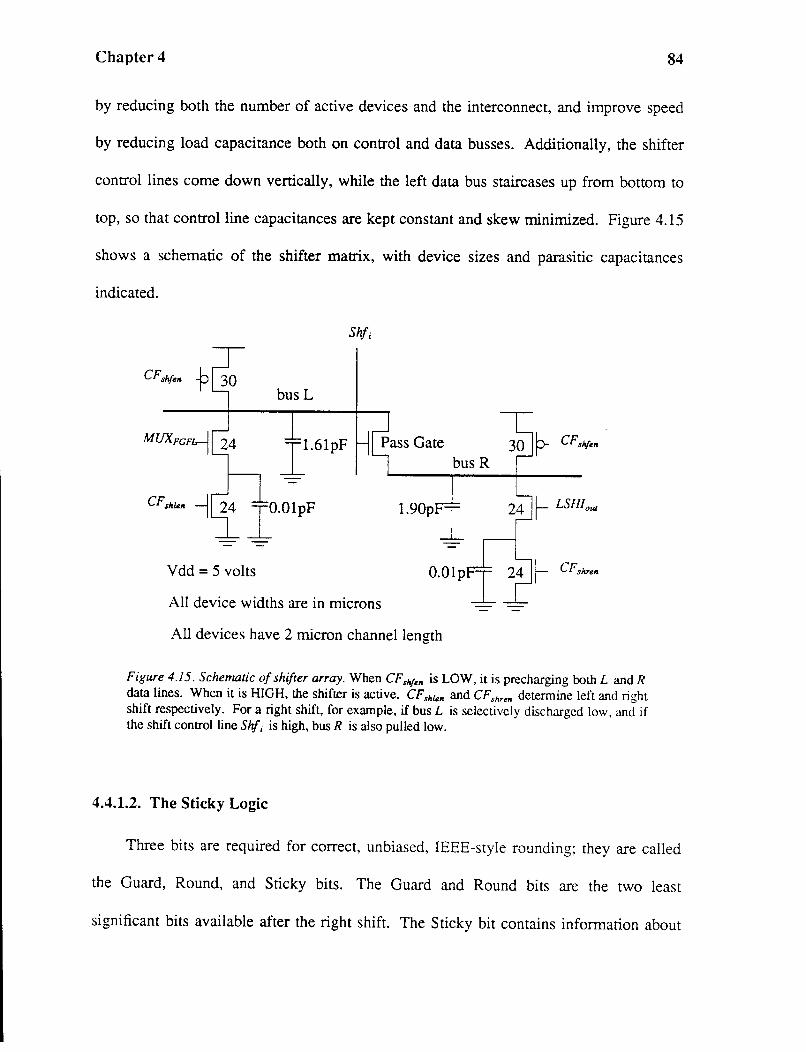
Chapter 4 84
by reducing both the number of active devices and the interconnect, and improve speed
by reducing load capacitance both on control and data busses. Additionally, the shifter
control lines come down vertically, while the left data bus staircases up from bottom to
top, so that control line capacitances are kept constant and skew minimized. Figure 4.15
shows a schematic of the shifter matrix, with device sizes and parasitic capacitances
indicated.
Vdd = 5 volts
All device widths are in microns
All devices have 2 micron channel length
Figure 4.15. Schematic of shifter array. When CFslifen is LOW, it is precharging both L and R data lines. When it is HIGH, the shifter is active. CFshlen and CFshren determine left and right shift respectively. For a right shift, for example, if bus L is selectively discharged low, and if the shift control line Shfi is high, bus R is also pulled low.
4.4.1.2. The Sticky Logic
Three bits are required for correct, unbiased, IEEE-style rounding; they are called
the Guard, Round, and Sticky bits. The Guard and Round bits are the two least
significant bits available after the right shift. The Sticky bit contains information about
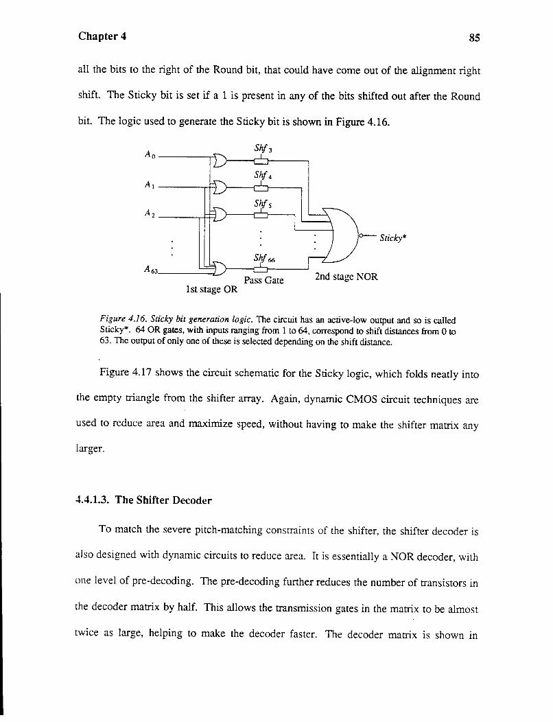
Chapter 4 85
all the bits to the right of the Round bit, that could have come out of the alignment right
shift. The Sticky bit is set if a 1 is present in any of the bits shifted out after the Round
bit. The logic used to generate the Sticky bit is shown in Figure 4.16.
Pass Gate 2nd stage NOR 1st stage OR
Figure 4.16. Sticky bit generation logic. The circuit has an active-low output and so is called Sticky*. 64 OR gates, with inputs ranging from 1 to 64, correspond to shift distances from 0 to 63. The output of only one of these is selected depending on the shift distance.
Figure 4.17 shows the circuit schematic for the Sticky logic, which folds neatly into
the empty triangle from the shifter array. Again, dynamic CMOS circuit techniques are
used to reduce area and maximize speed, without having to make the shifter matrix any
larger.
4.4.1.3. The Shifter Decoder
To match the severe pitch-matching constraints of the shifter, the shifter decoder is
also designed with dynamic circuits to reduce area. It is essentially a NOR decoder, with
one level of pre-decoding. The pre-decoding further reduces the number of transistors in
the decoder matrix by half. This allows the transmission gates in the matrix to be almost
twice as large, helping to make the decoder faster. The decoder matrix is shown in
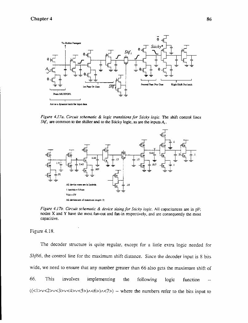
Chapter 4
To Sltifta Pu.p
i
Rigbt Shift Out latclt
Prcm MUXFGFL
Act u a dynamic latclt far illput dol&
Figure 4.17a. Circuit schematic & logic transitions for Sticky logic. The shift control lines Slifi are common to the shifter and to the Sticky logic, as are the inputs Ai.
All device 1izca arc in lambda
llunbda= 0.8um
Vdd=5V
All devices""' of minimum length (2)
Figure 4.17b. Circuit schematic & device sizing for Sticky logic. All capacitances are in pF; nodes X and Y have the most fan-out and fan-in respectively, and are consequently the most capacitive.
Figure 4.18.
86
The decoder structure is quite regular, except for a little extra logic needed for
Shf66, the control line for the maximum shift distance. Since the decoder input is 8 bits
wide, we need to ensure that any number greater than 66 also gets the maximum shift of
66. This involves implementing the following logic function
(( <l>v<2>v<3>v<4>v<5> )1\<6> )1\<7>) -- where the numbers refer to the bits input to
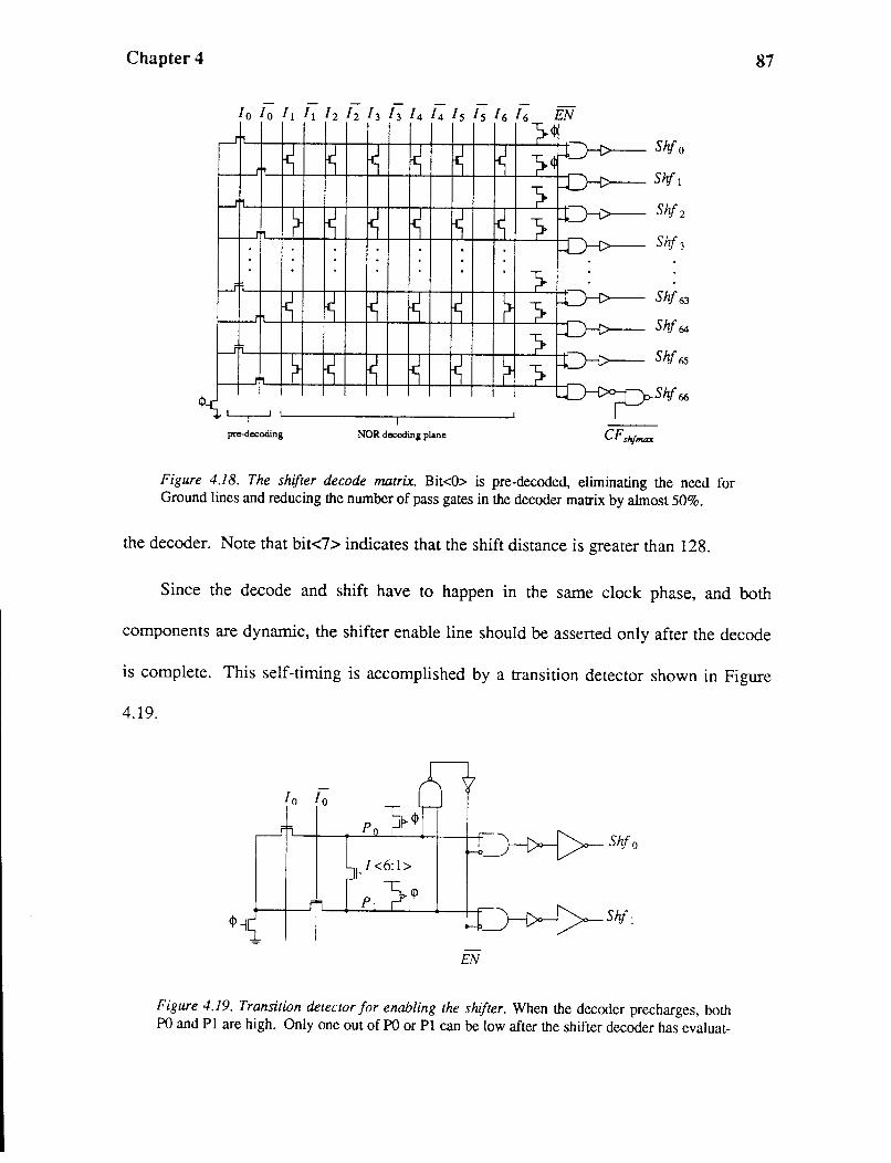
Chapter 4 87
,-1,
~ ~ ~ ~ r--- ____],
~
~ ~ ~ ~ r---__,, .
1-----i
~ ~ ~ ~ r--- --'
~
~ ~ ~ ~ r---1-----'
~ I pre-decoding NOR decoding plane
3 ~
~ 6 . .
~ .~
~ ~
}<ll }-_¢
}
~.
} } }
}
_(J--t>-
H-i:::
~=:K>---
-LJ:::
~=:K>---
D-t>--~=:K>---
Shf 63
Shf 64
Shf 65
Shf 66
Figure 4.18. The shifter decode matrix. Bit<O> is pre-decoded, eliminating the need for Ground lines and reducing the number of pass gates in the decoder matrix by almost 50%.
the decoder. Note that bit<7> indicates that the shift distance is greater than 128.
Since the decode and shift have to happen in the same clock phase, and both
components are dynamic, the shifter enable line should be asserted only after the decode
is complete. This self-timing is accomplished by a transition detector shown in Figure
4.19.
EN
Figure 4.19. Transition detector for enabling the shifter. When the decoder precharges, both PO and Pl are high. Only one out of PO or Pl can be low after the shifter decoder has evaluat-

Chapter 4 88
ed, and this in turn enables the shifter control lines.
Table 4.6 summarizes simulation results for the 67-bit shifter. Note that the shifter
array and sticky-bit generator evaluate in parallel, once the shift decoding is completed.
Table 4.6: Timing for 67-bit bi-directional shifter.
Component Delay (ns)
Shift Decoder 7.8 Shifter Array 8.5 Sticky Logic 10.9
4.4.2. The Leading One's Detector
The task of a leading one's detector is to find the position of the leading nonzero
digit and output the shift amount coded in binary format to the shifter, for the
normalization left shift. The same output is used by the exponent unit to determine the
result exponent. When no leading 1 is found, the detector signals an all-0 fraction, acting
as an allO-detector.
A fast and compact leading 1 's detector poses a design challenge; in past designs,
this module has tended to be one of the slowest and most expensive components in a
fraction datapath [Tayl83]. Our design goal was that it evaluate in one phase, and it
turned to be fast enough and very compact as well. Dynamic circuits were used here,
providing adequate speed and density. Figure 4.20 shows the logical formulation of the
solution for an example 8-bit detector. With some transformations, the logic is reduced
to a cascade of OR/NOR gates with varying fan-in, which can be very efficiently
implemented using parallel N channel devices.
Domino AND gates [Kram82] with maximum fan-in of 4 were found to be optimal
in area and delay, and the 67-bit detector is implemented in 4 stages. The inverters at

Chapter 4
Bo Bo
B1 Bl ----+....,_ B2 B2
B3 B 3 ------t--o_
B4 B4 Bs B 5 --~,...,_~ .----*-+-+- S 2 = B 1-B 6·B s B6 B6
B1 B 7 -----------:~"*-So= B 7
ANDPI..ANB OR PLANE
Figure 4.20. Logic for detecting the position of a leading 1. Crosses in the AND plane and OR plane represent AND and OR gates respectively. This eight-bit example shows three successive levels of AND gates to form the terms S 7 to S 0, while 4-input OR gates generate the outputs 0 2 to Oo.
89
each stage are skewed with stronger N channels (ratio of P:N is 1 :3) to rrumrmze
sensitivity to charge sharing, and even though the worst-case voltage drop on a charged
node was 1.46 volts, the circuit retained a noise margin of at least 1.0 volt.
A smaller fan-in results in additional stages, but the circuit is less process-sensitive.
Again, in the layout of the Domino AND gates, the width of the long chain of N-channel
inputs is scaled with the smallest at the top, to further increase speed by 15% by reducing
capacitance [Shoj85]. The circuit schematic of the 1 's detector is shown in Figure 4.21.
..t.S. Rounding
The shifter is primarily responsible for generating the three rounding bits on the
right alignment shift for addition and subtraction. Generating these bits for multiply and
divide are a little more involved, especially for iterative algorithms, and is discussed in

Chapter 4
VDDisSV
Devices""' of minimwn leJ181h (2)
Allsiza ue in lambda
1 lombda = 0.8 um
All Capocitanco val.- ..., in pi'
Figure 4.21. Circuit implementation for leading 1 's detector. The Domino AND gates are restricted to a maximum of four inputs and an extra pair of buffers is inserted between the second and third AND stages to drive the large capacitance on node X.
90
the next chapter. In any case, a selector chooses between the add/subtract and
multiply/divide units' rounding bits, depending on the instruction executed, and latches
them in as part of the intermediate result.
The rounding bits are sent to a PLA together with the intermediate result's least
significant bit (LSB) and two sign bits -- the sign of the intermediate result and the sign
of the final result. The user-specified two-bit rounding mode is also input to the rounding
PLA, leading to eight total inputs. The PLA then determines ( 1) the least significant bit
of the result, and (2) whether the intermediate result requires to be incremented. The
PLA also generates the two rounding tag bits, which signal whether rounding was done.
and if so, whether an increment was necessary. Thus the PLA provides four outputs.
The IEEE Standard provides four different rounding options or modes: unbiased
rounding to the nearest LSB, two modes of directed rounding to plus and minus infinity,
and truncation. Depending on the rounding bits, a positive intermediate result could
require an increment for rounding up to plus infinity or to nearest even, while a negative
Chapter 4 91
intermediate result could require to be incremented to round down to negative infinity or
to the nearest even LSB. Truncation, the fourth rounding mode, is the only one which
simply retains the present value of the LSB and does not require an increment.
The rounding PLA as described above requires eight inputs and four outputs, and
when optimized has 28 product terms. With extra logic at the input and output, the
intermediate sign bit and even the LSB could be generated outside the PLA, reducing the
total number of inputs/outputs by one or two. This, in turn, reduces the product terms
from 28 to 15 for one less input, or 11 for one less input and one less output. We still
implemented the larger PLA, because the design was the most regular and led to very
little increase in area or delay while reducing design time.
4.6. Summary
Datapath design considerations for fast addition and subtraction in VLSI floating
point units are presented in this chapter. The main components that are area-intensive
and time-consuming are identified, and specific design techniques are developed to yield
area-time efficient solutions. The SPUR FPU, implemented in 2 micron CMOS
technology, is used as a case study, where operation times are optimized for extended
precision arithmetic. Design for the very wide data widths in floating-point units present
interesting challenges, and these are explored in relation to specific design examples.
The design consequences of decoupling memory operations from arithmetic
functions are explored, and the area-time complexity of unpacking and packing data on
loads and stores are presented. A register cell with two read and two write ports is
shown, together with its pseudo-static decoder, designed specifically for very wide data

Chapter 4 92
widths. The 87-bit-wide 16-word register file has an access time of 17.7 nanoseconds
and occupies 4% of the entire chip area.
The datapath components for fast exponent evaluation are presented, including a
dual-subtracter and overflow/underflow detector for multiple operand precisions. An
optimized parallel-prefix adder is designed, based on a more realistic model of fan-out
and interconnect delay, which is especially suitable for large data widths. Buffers of
variable size are inserted in the carry-computation array to balance critical delay paths at
every carry stage, leading to gains in both area and time. Our 66-bit adder occupies 2.5
square mm and the worst case carry computation requires 25 nanoseconds.
A 67-bit bi-directional single-stage shifter design is shown, together with a fast and
compact decoder matrix including a self-timed enable circuit to allow single-phase
operation of both decoder and shifter. The barrel shifter is almost twice the size of the
66-bit adder, making it the single largest datapath component, but it evaluates in just 18.7
nanoseconds. A novel design is also presented for the generation of the Sticky bit, which
requires no extra area and marginally impacts the shifter speed.
Design of rounding logic to support the different rounding modes of the IEEE
Standard are discussed, including a way to eliminate an extra increment delay due to
rounding. The design of a fast and area-efficient leading-one's detector is presented, that
determines the position of the leading one in a 67-bit word in 15 nanoseconds and
requires 2.3 square mm.
Hu [Hu87] helped with the layout and circuit simulation of some of these datapath
components.
Chapter 4 93
4.7. References
[Bren82] R. P. Brent and H. T. Kung, A Regular Layout for Parallel Adders, IEEE Trans. on Computers, Vol. C-31, No. 3(March 1982), pp. 260-264.
[Han87] T. Han and D. A. Carlson, Fast Area-Efficient VLSI Adders, Proc. Eighth IEEE Int' I. Symposium on Computer Arithmetic(May 1987), pp. 87-94.
[Hu87] T. Hu, Circuit Design Techniques for a Floating-Point Processor, Computer Science Division (EECS) Report No. UCB/CSD 87/372, University of California, Berkeley (September 1987).
[Kram82] R. Krambeck, C. Lee and H. Law, High-Speed Compact Circuits with CMOS, IEEE Journal of Solid-State Circuits, Vol. SC-17, No. 3 (June 1982), pp. 614-619.
[Ladn80] R. E. Ladner and M. J. Fischer, Parallel Prefix Computation, JACM, vol. 27, No. 4(0ctober 1980), pp. 831-838.
[Oust83] J. Ousterhout, Crystal: A Timing Analyzer for NMOS VLSI Circuits, Proc. Third Caltech Conference on VLSI(1983), pp. 57-70.
[Shoj85] M. Shoji, FET Scaling in Domino CMOS Gates, Proc. International Symposium on Circuits and Systems(June 1985).
[Tayl83] G. S. Taylor, Arithmetic on the ELXSI System 6400, Proceedings of IEEE 1983 6th Symposium on Computer Arithmetic(1983), pp. 110-115.
[Wei85] B. W. Y. Wei, C. Thompson andY. Chen, Time-Optimal Design of a CMOS Adder, Technical Report No. UCB/CSD 86/252, U.C. Berkeley (August, 1985).
5 Multiply/Divide Datapath Design Considerations
94
This chapter continues the discussion on datapath design, emphasizing techniques
for the design of high-performance multiply and divide units used in building floating
point processors in VLSI. Area-time tradeoffs between various serial, recursive and
parallel algorithms for multiply and divide are considered, using the SPUR FPU
implementation as a case study. Details of the algorithms chosen, timing and overlap of
pipeline stages, hardware needed to support IEEE-style rounding, and logic and circuit
design issues are presented, as well as the exploration of design techniques for
minimizing area and maximizing throughput.

Chapter 5 95
5.1. Implementation Considerations
Recent papers [Gama86], [Uya84] show that 32 bit multipliers require about 40,000
transistors, and with current 2 micron technology, take up about 30 square mm. Full 64-
bit array multipliers are still difficult to integrate onto a single chip. Even if we could
build a multiplier that computed in a single cycle, it would be difficult to build a
proportionately fast divider, and divide times must improve with multiply, otherwise
algorithm designers will be tempted to devise means to avoid division. Using the relative
frequencies in Table 2.6, multiply and divide together account for 40% of the operations,
and so should preferably be allocated close to that percentage of the total datapath area.
Given the above area constraint, iterative algorithms seem more feasible than purely
combinational algorithms in present-day technology. If multiplication and division can
share much of the hardware, more aggressive algorithms can be chosen within the same
area budget.
Figure 5.1 shows the entire datapath for multiplication and division. Modules that
are density-critical are designed using dynamic circuits, and modules that have rigid
timing constraints and where precharge times cannot be overlapped with evaluation
times, are designed using static circuits. The hardware blocks that are not shared are the
multipler Booth recoder and the divider quotient selector and accumulator, accounting
for 8% of the entire multiply/divide datapath; the rest of the hardware is common to both
multiplication and division.

Chapter 5
----------------- -------------------+-- ----~ :··----·;J;·-·····:
·-·----~------~-- ------~~~~------- __ !_j \::, Bo~th \::, I 1-w ~_I! .., I c..,..MJ>r/IM' I i i I Llldl i I h ~W« ~7 \ 1 rf
•·······-········ ·····W"""i,··W"""i,······ ·····.:, : I Mux :
m ~~~*-~:··-:3·-··+····--·; ~~~~
VII n
vm
v
I
I
IX
I Sbift.Rl I Round
VI
•················ .................... ~ .... 1
a .. A
Figure 5.1. The Multiply-Divide Datapath. The datapath has the following sections: the multiplier 8-bit right shifter (!); input latches for holding the operands and the complement of the multiplier/divisor (II); multiplicand/divisor select (IJI); carry-save-adder tree (IV); partial sum and partial carry formation (V) and quotient accumulation (VI). The Booth encoder (VII), quotient selection (VIII) and generation of rounding bits (IX) are off to the right side, with (/), (VII), and (VIII) being the only components not shared between multiplication and division.
96

Chapter 5 97
5.2. The Multiplier
As described in Chapter 3, it is not feasible to build an FPU with an array multiplier
that could compute a product of two extended-precision (64-bit) operands in a single
cycle with currently available technology. We considered several iterative schemes
including smaller arrays but it was difficult to integrate even a 32 x 32 array within our
area budget for multiplication and division. Consequently, we moved to a 64 x 8
iterative algorithm that evaluates an extended-precision product in nine iterations.
5.2.1. The Algorithm
Figure 5.2 illustrates the formation of the multiplier partial products. The multiplier
is shifted right by eight at the beginning of every iteration, providing the modified Booth
recoder with a new byte. The recoder views the byte as consisting of four triplets
overlapping each other by one bit, and each triplet is recoded to indicate one of five
possible multiples of the multiplicand: ±1, ±2 or zero times the multiplicand. The four
sets of outputs of the Booth recoder from the four overlapping triplets control a set of
four multiplexors, selecting the proper multiples of the multiplicand for each triplet.
Each multiplicand multiple is shifted left two bits from its less significant multiplicand
multiple, and all are sign-extended to 75 bits, which is the maximum length of the partial
product registers.

Chapter 5
CSA <0> ~s s!l~·Q~
CSA<l> ~s <!ll·Q>
CSA<2> Hs sftHl~
CSA <3> ~s sZJ·Q~
Master I I . 75
Slave I H 67 8 I : i
Master 2 I ! 75 16
Slave 2 r 67 16
Slave 8 67 64 :
Master 9 F o-4 64 lLiGJ• OR ~ II Zeros Sticky Bit
Figure 5.2. Forming the Product of two 64-bit operands. The width of the CSA, multiplexors and PPS/PPC are 75 bits. After right-shifting 8 bits, the sum of the two partial products is 67 bits (66 bit magnitude and 1 sign bit).
98
The four multiples of the multiplicand are added to the partial 'sum' and 'carry'
terms of the previous iteration, using four rows of carry-save-adders. These adders
postpone the need for complete product evaluation until the very last iteration, helping to
avoid carry propagation delay from determining the speed of an iteration. The partial
'sum' and 'carry' are shifted left 8 bits and 7 bits respectively, when looping them back
to be the new inputs of the CSA for the next iteration. The multiplexers and CSA must
be fully sign-extended to the most significant side, since the operands are in two's
complement form and can be both positive and negative. A carry-look-ahead adder is
necessary twice for multiplication -- to form the complement of the multiplicand and to
form the final product -- and instead of duplicating it here, the fraction adder for
add/subtract is used instead. This increases the setup and completion times by one

Chapter 5 99
cycle, but reduces the area of the unit by 14%.
5.2.2. The Multiply Inner Loop
The four rows of carry-save-adders are in the critical path for the multiplier inner
loop, and Figure 5.3 shows the organization of the CSA tree. To reduce the CSA delay,
CSA rows 0 and 1 evaluate in parallel, reducing the net delay to three CSA stages. This
makes the interconnect less regular, but provides a 25% speed improvement in the CSA
stage. For the divider, only one row of the CSA tree is necessary, and so we can use the
isolated CSA row 0 to advantage.
Mux3<1> Mwt3<0>
Mux2<3> Mux2<2> Mux2<1> Mux2<:0>
OMuxO<l> MuxO<O>
Row 1
Row2
Row3
RowO
Figure 5.3. Least Significant Bits of the CSA Tree. CSA row 0 has MuxO and the partial product sum and carry vectors as inputs, while CSA row 1 gets its inputs from Muxl, Mux2, and Mux3. Since all six inputs are available at the same time, these two CSA rows can compute simultaneous! y.
In the multiplier inner loop, multiplicand selection is overlapped with shifting and
rounding the partial product vectors. During each cycle, two phases are for signals
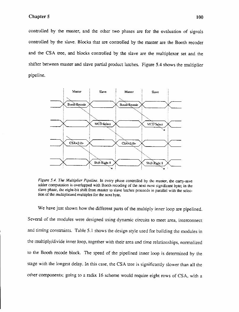
Chapter 5 100
controlled by the master, and the other two phases are for the evaluation of signals
controlled by the slave. Blocks that are controlled by the master are the Booth recoder
and the CSA tree, and blocks controlled by the slave are the multiplexor set and the
shifter between master and slave partial product latches. Figure 5.4 shows the multiplier
pipeline.
Master
B~tft-R.c;code ·· ... --
Slave
··-·f-·---. ,.------.. : r--'·::..,· .,...----..
MCD·Select ·. ·.
Master
·· .... Bootn'-Recode ·.
···i.
cS'A><J.:O> ·. '• ·.
: · .. . .. r-------..!r-··~-~----..
csA-~v>>
··.: ., ...
'•
r------....,_ i r-··-_···_,_· • ......--------.
Shif;Right 8 ··.,.
Slave
·.,.
Figure 5.4. The Multiplier Pipeline. In every phase controlled by the master, the carry-save adder computation is overlapped with Booth recoding of the next most significant byte; in the slave phase, the eight-bit shift from master to slave latches proceeds in parallel with the selection of the multiplicand multiples for the next byte.
We have just shown how the different parts of the multiply inner loop are pipelined.
Several of the modules were designed using dynamic circuits to meet area, interconnect
and timing constraints. Table 5.1 shows the design style used for building the modules in
the multiply/divide inner loop, together with their area and time relationships, normalized
to the Booth recode block. The speed of the pipelined inner loop is determined by the
stage with the longest delay. In this case, the CSA tree is significantly slower than all the
other components; going to a radix 16 scheme would require eight rows of CSA, with a

Chapter 5 101
delay of five stages. This would double the CSA area requirement, and increase the
delay by 67%. Clearly, carry-save adders become the limiting factor in the speed of
high-radix iterative multipliers.
Table 5.1: Area-Time Relationships of Multiply Function Modules Function Design Style Area Time
Booth Recode Dynamic 1.0 1.0 MCD Select Dynamic 2.6 0.9 CSA Tree Dynamic 9.9 4.3 Partial Sum & Carry Static 8.7 0.5
Area and time are normalized to the Booth recode block. The CSA, for example, is almost ten times larger and more than four times slower than the Booth Recode block.
The four rows of carry-save-adders take the longest time among the pipeline
components. The dynamic CSA design was 16% smaller than its static counterpart, and
was still able to meet the timing requirements. If we went to a more aggressive clocking
scheme, it would be feasible to build the four multiplexors and the CSA tree static, and
modify the pipeline to have only two stages. One stage could perform Booth recoding
and MCD selection, while the other could do CSA evaluation and the right shift. Not
only could the disparity between the stages become smaller, but we could also utilize two
out of the four clock non-overlap times.
5.2.3. Rounding
The ability to perform unbiased rounding with error less than half a unit in the last
place requires three extra bits, called the Guard, Round and Sticky bits. The G and R bits
are used if the intermediate result of a division is between .5 and 1 and hence requires a
one-bit normalizing left shift. The Sticky bit is equal to zero only if all subsequent bits in

Chapter 5 102
a result of infinite precision are zero and is used to identify the half-way case for
unbiased rounding.
During a multiply operation, the vectors containing the partial products are shifted
right eight bits before being returned for the next iteration. These two eight-bit quantities
are added together, and ORed to form the 'partial sticky' bit. This is fed back to the
rounding adder for the next iteration. At the end of the final rounding addition, bit<O> of
the result is the most significant bit of the rounding adder result, followed by the G bit.
The R bit is zero, since the result must be in a range between 1 and 4. The OR of the
remaining bits of the rounding adder provides the Sticky bit, as shown in Figure 5.5.
Since each iteration takes. half a cycle in this pipelined scheme, partial product
evaluation takes four and a half cycles. It takes almost that long, again, for evaluating
the complement of the multiplicand, the final carry-propagate addition and the rounding,
making the total multiply latency eight cycles. Some of this can be saved by duplicating
the fraction ALU in the multiply/divide unit, and also duplicating the rounding PLA that
generates the least significant bit. Currently, both of these are shared with the fraction
unit; if these were duplicated, the potential time saving can be two cycles or 20%.

Chapter 5
Iterations 1 to 8 Iteration 9
PPS<7:0> PPC<7:0> PPS<7:0> PPC<7:0>
Cin Round Adder
Cout<6>
(Frac Cin)
Sticky bit
Figure 55. Multiply Rounding. For the first eight iterations, the L, G, and S bits are ORed to form the temporary Sticky bit, which in turn is ORed with the six least significant bits out of the round adder in the next iteration. The carry out of bit<6> (Guard bit position) in the last iteration becomes the carry input to the adder summing the partial product sum and carry vectors in the fraction unit.
103
The rounding bits generated at the end of the final iteration are sent back to the
add/sub fraction unit, together with the partial product sum and carry bits. The partial
product bits are added in the carry-propagate full adder to form the intermediate result,
while the rounding bits are ·multiplexed in directly. The intermediate result then goes
through the process of rounding and normalization, just like any other arithmetic
instruction.

Chapter 5 104
5.3. The Divider
Addition and multiplication in VLSI arithmetic accelerators have received a lot of
attention lately, but not much work has been reported to build fast division schemes in
VLSI. As discussed in Chapter 3, restoring divide is the least expensive approach for
radix-two division, but the cost increases exponentially with the number of bits generated
per iteration [Gosl80], and the same is true of parallel-serial schemes [Zura81]; on the
other hand, the problem with multiplicative inverse schemes is that quotients and
remainders are incorrectly rounded. Quotient digit selection is the focus of attention of
SRT division [Robenson65] [Atkins67], and redundancy in the representation of quotient
digits allows corrections in subsequent iterations, eliminating the need for back-tracking
after every remainder iteration. In comparison with other algorithms, higher radix SRT
division provides significant gains in area and speed, provided compact quotient
selection logic is designed, and each iteration can be pipelined, with overlapping stages
like partial remainder formation and quotient selection evaluating concurrently.
5.3.1. The Algorithm
The algorithm implemented in our FPU is based on radix-four non-restoring
division and uses estimates of the divisor and partial remainder for quotient estimation.
A redundant representation is used to represent the radix-four quotient digits, while there
is no redundancy in the partial remainder. Plotting the partial remainder against the
divisor (P/D plots), it can be shown that six bits of remainder and four bits of divisor are
sufficient to determine the next quotient digit, guaranteeing error bounds will not be
exceeded [Frei61] [Atki68].
Chapter 5 105
The division is done iteratively, with two quotient bits computed per iteration, with
the equation expressed as follows:
where j =index of the recursive loop <33:0>,
Pi =partial remainder after the jth loop,
Po =dividend,
qU+I) =quotient digit after the jth loop,
d = divisor, and
r =radix <4>.
Eight bits of partial remainder 'sum' and 'carry' vectors are added and the six most
significant bits of this truncated partial remainder are sent to the quotient selection logic,
together with the four most significant bits of the divisor. The quotient selector in turn
generates three bits, representing one of the five possible values of the quotient digit.
Two registers store the generated quotient bits at each iteration, one holding the positive
quotient values and the other holding the negative quotient values. A final carry-look
ahead subtraction of the negative quotient from the positive quotient is necessary to
generate the true quotient. The output of the quotient selection logic is also decoded to
control a multiplexor that decides what multiple of the divisor to use for the next
iteration. Figure 5.6 shows how the positive and negative quotients are formed.
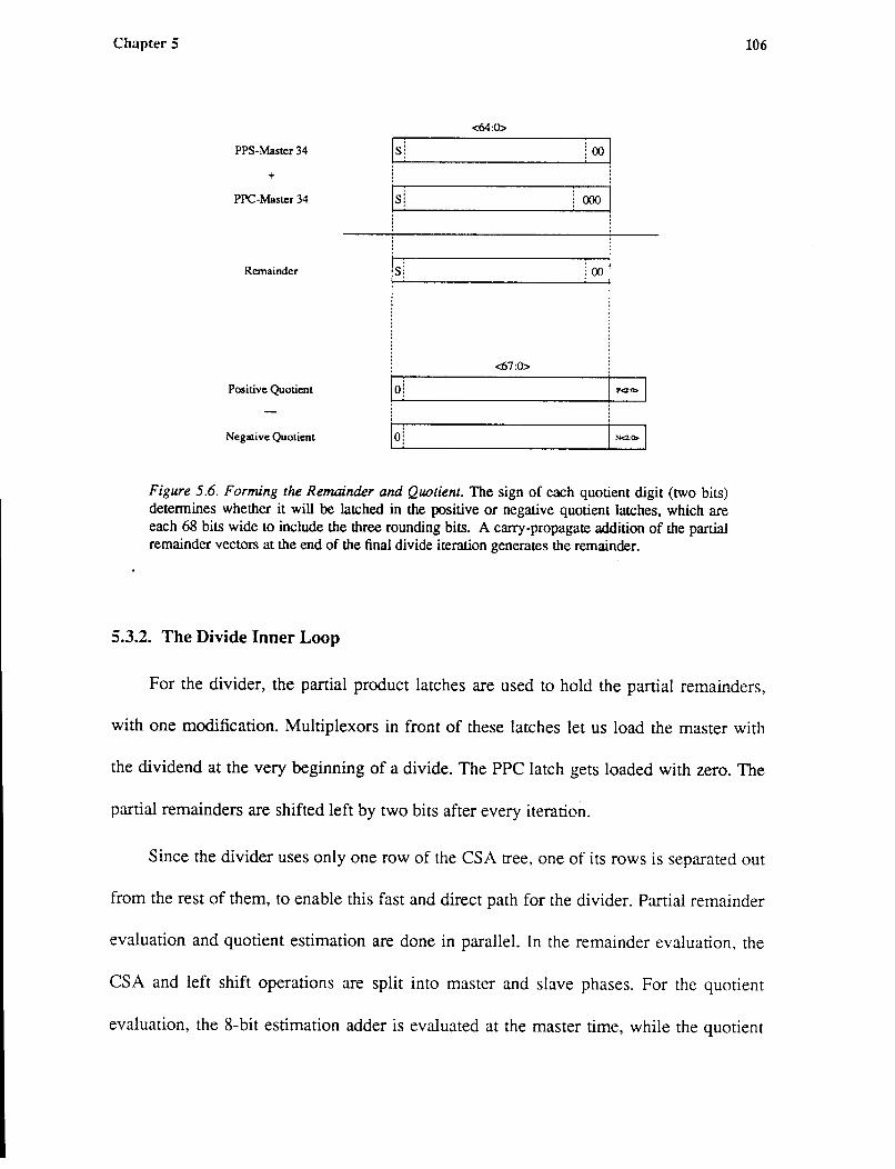
Chapter 5
<64:0>
PPS-Master 34
+
PPC-Master 34
Remainder
<.67:0>
Positive Quotient
Negative Quotient
Figure 5.6. Forming the Remainder and Quotient. The sign of each quotient digit (two bits) determines whether it will be latched in the positive or negative quotient latches, which are each 68 bits wide to include the three rounding bits. A carry-propagate addition of the partial remainder vectors at the end of the final divide iteration generates the remainder.
5.3.2. The Divide Inner Loop
106
For the divider, the partial product latches are used to hold the partial remainders,
with one modification. Multiplexors in front of these latches let us load the master with
the dividend at the very beginning of a divide. The PPC latch gets loaded with zero. The
partial remainders are shifted left by two bits after every iteration.
Since the divider uses only one row of the CSA tree, one of its rows is separated out
from the rest of them, to enable this fast and direct path for the divider. Partial remainder
evaluation and quotient estimation are done in parallel. In the remainder evaluation, the
CSA and left shift operations are split into master and slave phases. For the quotient
evaluation, the 8-bit estimation adder is evaluated at the master time, while the quotient
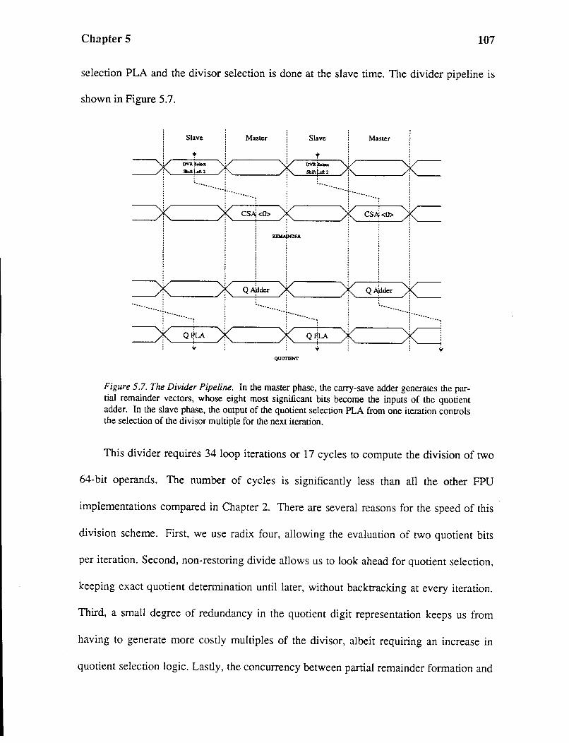
Chapter 5 107
selection PLA and the divisor selection is done at the slave time. The divider pipeline is
shown in Figure 5.7.
Slave Master Slave Master
'------------1·-----------:
csAi <0>
~...... :
r------------,·--r-------·---: csAi<O>
Q 4Ider ............................. :: ................... ..
.... : r----i----..
Q~LA
.. .......
QUarn!NT
Figure 5.7. The Divider Pipeline. In the master phase, the carry-save adder generates the partial remainder vectors, whose eight most significant bits become the inputs of the quotient adder. In the slave phase, the output of the quotient selection PLA from one iteration controls the selection of the divisor multiple for the next iteration.
This divider requires 34 loop iterations or 17 cycles to compute the division of two
64-bit operands. The number of cycles is significantly less than all the other FPU
implementations compared in Chapter 2. There are several reasons for the speed of this
division scheme. First, we use radix four, allowing the evaluation of two quotient bits
per iteration. Second, non-restoring divide allows us to look ahead for quotient selection,
keeping exact quotient determination until later, without backtracking at every iteration.
Third, a small degree of redundancy in the quotient digit representation keeps us from
having to generate more costly multiples of the divisor, albeit requiring an increase in
quotient selection logic. Lastly, the concurrency between partial remainder formation and

Chapter 5 108
quotient selection significantly increases algorithm efficiency. Table 5.2 shows the
relative area-time cost for different sections of the divide pipeline, normalized to the
divisor select block.
Table 5.2: Area-Time Relationships of Divide Function Modules Function Design Style Area Time
Divisor Select Dynamic 1.0 1.0 CSARow Dynamic 4.1 3.2 Quotient Adder Static 0.4 3.5 Quotient PLA Static 0.5 4.8 Quotient Accumulate Static 6.4 0.8
Area and time are normalized to the divisor select block. The quotient PLA, for example, is half as large and almost five times slower than the divisor selector. Compared to Table 5.1 for the multiplier, the pipeline stages are more balanced here, with the quotient selection PLA taking about 35% longer than carry-save addition or quotient addition.
5.3.3. Quotient Selection
An integral part of the divide scheme is the logic for quotient selection. To keep the
quotient selection logic from becoming the critical path, the quotient adder and PLA
were split into two phases. The adder can now be dynamic, since it can be precharged
when the PLA evaluates, thereby saving area. The PLA that generates the two bits of
quotient per iteration, gets its inputs at the beginning of every slave phase and has to
evaluate the quotient bits by the end of that phase. To achieve this strict timing
requirement, we went with a pseudo-static PLA design. At the expense of a little DC
power, output evaluation can be done in a single phase time. There are ten inputs to the
PLA (six bits from the quotient adder, and four from the divisor) and three outputs (two
quotient bits and the sign bit). Two optimizations were done to reduce the size of the
PLA. First, the quotient sign bit is the same as the sign of the partial dividend, and hence
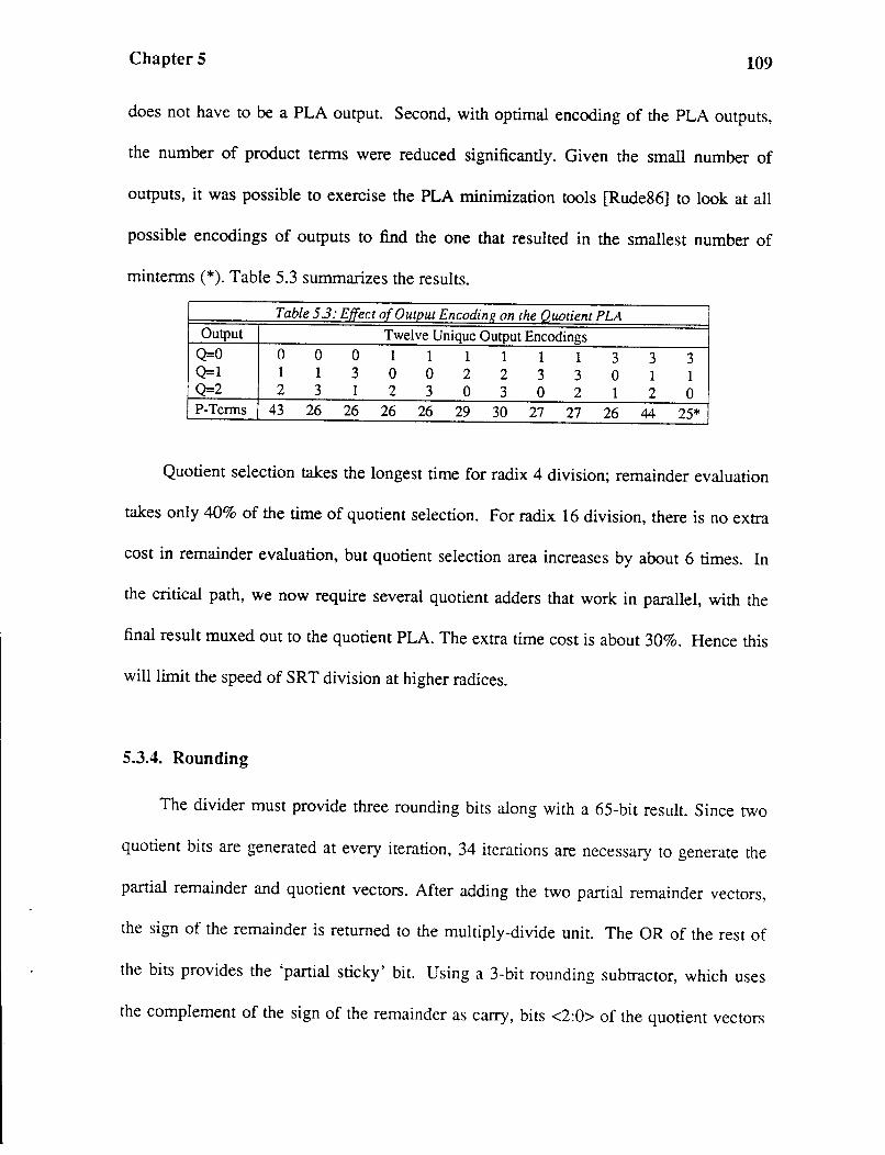
Chapter 5 109
does not have to be a PLA output. Second, with optimal encoding of the PLA outputs,
the number of product terms were reduced significantly. Given the small number of
outputs, it was possible to exercise the PLA minimization tools [Rude86] to look at all
possible encodings of outputs to find the one that resulted in the smallest number of
minterms (*). Table 5.3 summarizes the results.
Table 5.3: Effect of Output Encoding on the Quotient PLA Output Twelve Unique Output Encodings
Q=O 0 0 0 1 1 1 1 1 1 3 3 3 Q=1 1 1 3 0 0 2 2 3 3 0 1 1 Q=2 2 3 1 2 3 0 3 0 2 1 2 0 P-Tenns 43 26 26 26 26 29 30 27 27 26 44 25*
Quotient selection takes the longest time for radix 4 division; remainder evaluation
takes only 40% of the time of quotient selection. For radix 16 division, there is no extra
cost in remainder evaluation, but quotient selection area increases by about 6 times. In
the critical path, we now require several quotient adders that work in parallel, with the
final result muxed out to the quotient PLA. The extra time cost is about 30%. Hence this
will limit the speed of SRT division at higher radices.
5.3.4. Rounding
The divider must provide three rounding bits along with a 65-bit result. Since two
quotient bits are generated at every iteration, 34 iterations are necessary to generate the
partial remainder and quotient vectors. After adding the two partial remainder vectors,
the sign of the remainder is returned to the multiply-divide unit. The OR of the rest of
the bits provides the 'partial sticky' bit. Using a 3-bit rounding subtractor, which uses
the complement of the sign of the remainder as carry, bits <2:0> of the quotient vectors
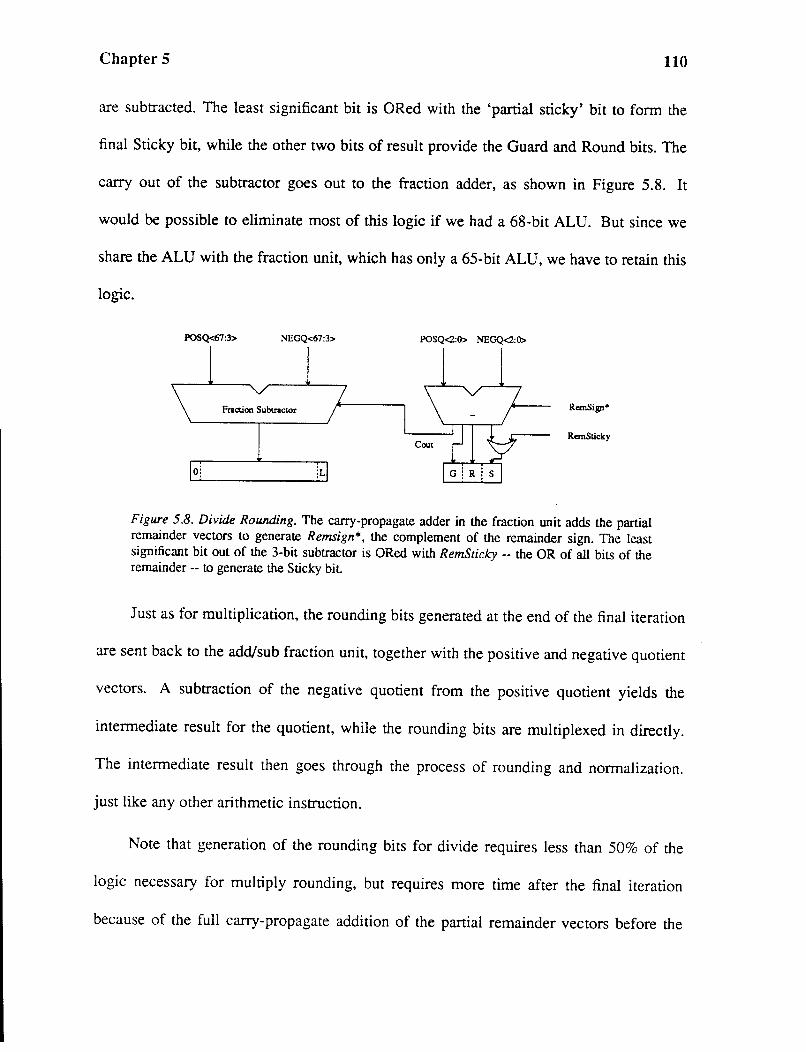
Chapter 5 110
are subtracted. The least significant bit is ORed with the 'partial sticky' bit to form the
final Sticky bit, while the other two bits of result provide the Guard and Round bits. The
carry out of the subtracter goes out to the fraction adder, as shown in Figure 5.8. It
would be possible to eliminate most of this logic if we had a 68-bit ALU. But since we
share the ALU with the fraction unit, which has only a 65-bit ALU, we have to retain this
logic.
POSQ<67:3> NEGQ<67:3> POSQ<2:0> NEGQ<2:0>
RemSign*
RomSticky
Figure 5.8. Divide Rounding. The carry-propagate adder in the fraction unit adds the partial remainder vectors to generate Remsign*, the complement of the remainder sign. The least significant bit out of the 3-bit subtractor is ORed with RemSticky -- the OR of all bits of the remainder -- to generate the Sticky bit
Just as for multiplication, the rounding bits generated at the end of the final iteration
are sent back to the add/sub fraction unit, together with the positive and negative quotient
vectors. A subtraction of the negative quotient from the positive quotient yields the
intermediate result for the quotient, while the rounding bits are multiplexed in directly.
The intermediate result then goes through the process of rounding and normalization.
just like any other arithmetic instruction.
Note that generation of the rounding bits for divide requires less than 50% of the
logic necessary for multiply rounding, but requires more time after the final iteration
. because of the full carry-propagate addition of the partial remainder vectors before the

Chapter 5 111
sticky bit can be generated.
5.4. Summary
This chapter presents techniques for the design and implementation of fast multiply
and divide units in VLSI. Algorithm area-time tradeoffs indicate that in presently
available 2 micron technology, it is difficult to implement large array multipliers on a
single chip, especially if it is to include a concomitantly fast divider. Consequently,
iterative algorithms are chosen for both multiply and divide.
Techniques are developed in this chapter for pipelining an iterative 64 x 8
multiplier to provide a 64 x 64 multiply in nine iterations, with two iterations per clock
cycle. Effectively, the inner loop provides the speed of a 64 x 16 multiplier, for
signifantly less area. This is made possible by overlapping pipeline stages, maximizing
throughput and resource utilization. Area-time tradeoffs are examined to determine
circuit design styles for optimum performance. A method is outlined for the formation of
the rounding bits-- Guard, Round and Sticky-- that requires minimal hardware without
slowing down the iteration pipeline, and proceeds in parallel with formation of the final
product.
The design of a radix-4 SRT divider is presented that computes the iterations for an
extended precision divide in 17 cycles. Even though two quotient bits are generated per
iteration, pipeline stages are overlapped to allow parallelism between quotient selection
and partial remainder formation, making it possible for four quotient bits to be generated
every cycle. Consequently, we have a divider that provides the speed of radix-16 division
for the area of only a radix-4 divider. Area-time tradeoffs of key divider blocks are
Chapter 5 112
presented, together with a method for optimizing the quotient generation PLA. The
hardware required to support IEEE-style rounding is also presented.
Significant hardware sharing occurs in the implementation of the multiplier and
divider, making it possible for the entire multiply-divide unit to occupy no more than
23% of the entire FPU area, while performing extended-precision multiplication and
division in 0.9 and 2.1 microseconds, respectively. Further speed enhancements in going
to similar but higher-radix iterative schemes will be limited by carry-save addition delay
for multiplication, and quotient selection delay for division.
Chapter 5 113
5.5. References
[Atki68] D. E. Atkins, Higher-Radix Division Using Estimates of the Divisor and Partial Remainders, IEEE Trans. Computers, Vol. C-17, No. JO(October 1968), pp. 925-934.
[Frei61] C. V. Freiman, Statistical Analysis of Certain Binary Division Algorithms, Proc.IRE, Vol. 49(January 1961), pp. 91-103.
[Gama86] A. E. Gamal, A CMOS 32b Wallace Tree Multiplier-Accumulator, Proc. ISSCC(February 1986), pp. 194-195.
[Gosl80] J. B. Gosling, Design of Arithmetic Units for Digital Computers, SpringerVerlag(1980).
[Rude86] R. Rudell, ESPRESSO, 1986 VLSI Tools, Report No. UCB/CSD 86/272 (1986).
[Uya84] M. Uya, A CMOS Floating Point Multiplier, IEEE J. Solid-State Circuits, Vol. SC-19, No.5(0ctober 1984), pp. 697-702.
[Zura81] J. Zurawski and J. B. Gosling, Design of High-Speed Digital Divider Units, IEEE Transactions on Computers, Vol. C-30, No. 9 (September 1981), pp. 691-699.

114
6 Control Design Considerations
This chapter presents design considerations for the control unit for memory and
arithmetic operations. Basic floating-point units are inherently datapath-intensive, and
the very wide data widths present unique challenges for control unit design.
The chapter begins with a presentation of the design considerations specific to the
FPU control unit, providing a basis for appreciating the major limiting factors of
performance in general. In previous chapters, the advantages of decoupling memory and
arithmetic operations have been enumerated; this chapter shows the overhead incurred in
control unit design to implement this parallelism between input/output and arithmetic.
· The design of the components of the FPU control unit, including instruction decoding,

Chapter 6 115
the load/store pipeline, the arithmetic state machine and cycle counter are presented,
together with tradeoffs for the partitioning of central control into multiple PLAs.
The discussion then moves to clocking issues in processor design, especially to the
considerations of charge redistribution and clock skew with dynamic circuit designs. As
processors evolve towards faster clock rates and smaller cycle times, the tolerances
between non-overlapping clock edges decrease. This makes the skew or relative delay
between clock edges even more pronounced, becoming a major factor in limiting further
speed-up of the processor clock rate. Different ways of minimizing and controlling clock
skew are investigated, and the results of applying a specific approach presented.
6.1. FPU Control Unit Overview
Conceptually, the control unit may be perceived to have three components:
instruction decoder, memory control and arithmetic control. The instruction decoder
receives control signals on the Instruction Bus and other interface signals, and decides to
activate either the memory control or the arithmetic control, as shown in Figure 6.1.
Load and Store instructions may be issued once every cycle, but since they take four
cycles to execute, these instructions need to be pipelined in four stages. Arithmetic
instructions, on the other hand, execute one at a time, but the number of execution cycles
vary with the kind of instruction. Memory and arithmetic instructions can also proceed
in parallel, requiring that memory and arithmetic control remain essentially independent.
Furthermore, all FPU instructions may be suspended or killed during execution, to
prevent the FPU from going into an inconsistent state if a trap occurs.
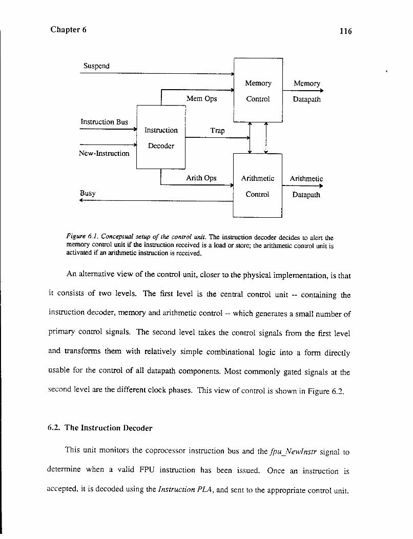
Chapter 6
Suspend
Memory Memory
I Mem Ops Control Datapath
Instruction Bus Instruction Trap
Decoder New-Instruction
I Arith Ops Arithmetic Arithmetic
Busy Control Data path
Figure 6.1. Conceptual setup of the control unit. The instruction decoder decides to alert the memory control unit if the instruction received is a load or store; the arithmetic control unit is activated if an arithmetic instruction is received.
116
An alternative view of the control unit, closer to the physical implementation, is that
it consists of two levels. The first level is the central control unit -- containing the
instruction decoder, memory and arithmetic control-- which generates a small number of
primary control signals. The second level takes the control signals from the first level
and transforms them with relatively simple combinational logic into a form directly
usable for the control of all datapath components. Most commonly gated signals at the
second level are the different clock phases. This view of control is shown in Figure 6.2.
6.2. The Instruction Decoder
This unit monitors the coprocessor instruction bus and the fpu _ Newlnstr signal to
determine when a valid FPU instruction has been issued. Once an instruction is
accepted, it is decoded using the Instruction PLA, and sent to the appropriate control unit.
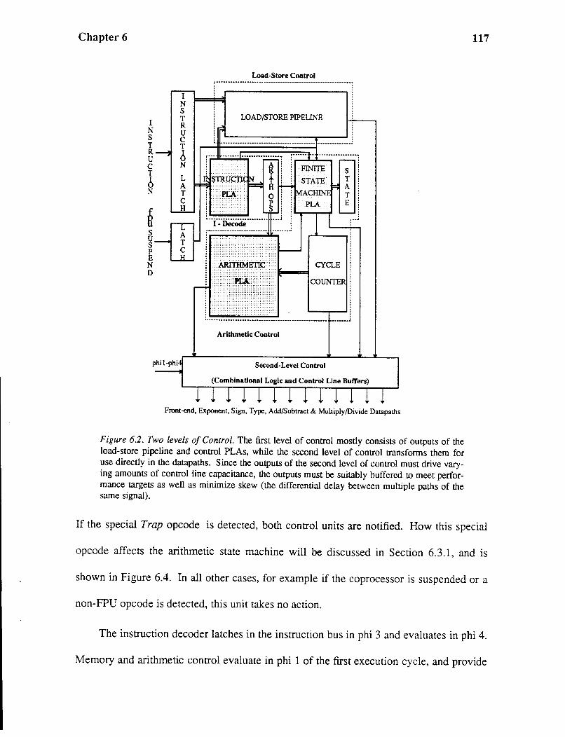
Chapter 6
I N s T R u c T
b N
R s u s p E N D
phil-phi
I N s T R u c T
b N
Load-Store Control
LOAD/STORE PIPELINE
Arithmetic Control
CYCLE
COUNT
Second-Level Control
(Combinational Logic and Control Line ButTers)
Front-end, Exponent, Sign, Type, Add/Subtract & Multiply/Divide Datapaths
Figure 6.2. Two levels of Control. The first level of control mostly consists of outputs of the load-store pipeline and control PLAs, while the second level of control transforms them for use directly in the datapaths. Since the outputs of the second level of control must drive varying amounts of control iine capacitance, the outputs must be suitably buffered to meet performance targets as well as minimize skew (the differential delay between multiple paths of the same signal).
117
If the special Trap opcode is detected, both control units are notified. How this special
opcode affects the arithmetic state machine will be discussed in Section 6.3.1, and is
shown in Figure 6.4. In all other cases, for example if the coprocessor is suspended or a
non-FPU opcode is detected, this unit takes no action.
The instruction decoder latches in the instruction bus in phi 3 and evaluates in phi 4.
Memory and arithmetic control evaluate in phi 1 of the first execution cycle, and provide
Chapter 6 118
all control signals from phi 2 on; the instruction decoder directly provides the datapath
with the signals needed in phi 1 of the first execution cycle.
The inputs of the instruction decoder are the outputs of latches holding the opcode
pins; these latches are in turn enabled by the fpuNewl nstr signal. The instruction decode
is done using a pseudo-static PLA, evaluating in phi 4. Two vectors of decoded opcode
signals are generated, one for memory and the other for arithmetic operations. A
memory operation is initiated only if the FPU is not suspended (fpuSuspend disasserted);
an arithmetic operation begins if the arithmetic unit is not busy (fpuBusy disasserted).
In addition to initializing the memory and arithmetic control units, the instruction
decoder unit controls the reading of the register file at the beginning of an arithmetic
operation. Since the register file is read in phi 1 of the first execution cycle, the decoder
unit must send the proper register specifiers to the register file in phi 4 of the fetch cycle.
Rather than inhibiting the register read, the arithmetic control unit disconnects the
register file busses from the internal data busses if the arithmetic datapath is busy.
6.3. Load-Store Control
Load and Store instructions can be issued once per machine cycle, and so the
memory control unit may receive input from the instruction decoder on every cycle.
These memory operations are considered to be part of the CPU pipeline, and the CPU
does the address computation for these instructions. The clock phases in which the FPU
does a Load or a Store are the same as for the CPU, so that the memory controller need
not distinguish between memory accesses for these two processors.
Chapter 6 119
Since an individual memory operation completes in four cycles, a four-stage
pipeline is necessary to allow a memory operation to be issued every cycle. These four
stages are successively called Decode, Execute, Memory and Write, and is shown in
Figure 6.3.
from Instruction PLA from Instruction Latch ,-- A~-------~ i 1 1 1 1 1 1 1 1 l Jl
texiJ;textl stsgl stdbl storeldcxtldextlldsgllddblload RD<0:3>
fpuNewlnstr* - clear DECODE STAGE latch - PID4
14~ ~v llV 0
MUX 1 sclectr- - ctrl-fpuSuscond
.J!t
~clear EXECUTE STAGE latchl- -MASTER PIDl
II ~v
clear EXECUTE STAGE latch~ i-SLAVE PID2 II
wK ~It
I 0 MUX 1 sclectl- I-ctrl-fpuS uscond
~lt
ctrl-TrapRecvd I MEMORYSTAGE clear MASTER late+- i-Pffil
II
J~
I MEMORY STAGE •clear SLAVE latch~ r- PHI2
IL j~
ctrl-fpuSuscond )-----,_
+lear WRITE STAGE latch PIDl
Jl MEMORY CONTROL LOGIC
Figure 6.3. The Load-Store Pipeline. Decode, execute, memory and write stages are shown, with the second and third stages consisting of master-slave latches. When the pipeline is suspended, say on a cache miss, information recirculates from slave to master instead of moving forward, provided the instruction has not reached the write stage.
Chapter 6 120
Each stage is active for exactly one machine cycle, and contains decoded opcode
information and the internal register specifiers. The pipeline is stalled when a Suspend
signal is detected, and it is cleared when a Trap instruction is decoded.
Since fpuSuspend arrives in phi 4 of a given cycle, the opcode pipeline cannot
change until the next phi 1. Master-slave latches are used to hold the pipeline stages, the
master latches are latched in phi 1, and the transition from master to slave occurs in phi
2. Since control signals that depend on the slave will not be stable until the next phase,
the slave latches provide signals needed for phases 3, 4 and the 1 of the next cycle; the
master latches only provide signals needed in phi 2. The feedback from slave to master
in the execute and memory cycles allows these stages to be repeated on a cache miss on
either CPU or FPU memory operations.
The CPU computes the addresses for all FPU memory operations, and data is
latched onto the FPU in phi 3 of the third or memory cycle on a LOAD. If a cache miss
occurs, the fpuSuspend signal recirculates the information in the memory stage of the
pipeline, and clear the write stage of the pipeline. On a STORE, data is sent out in phi 1
of the memory cycle, and held until a cache hit is indicated. The control signals for
driving the data pads in this case are derived from the second or 'execute' stage of the
pipeline, and this stage recirculates if there is need for pipeline suspension.
6.4. Arithmetic Control
While the Load-Store control unit handles multiple instructions of fixed execution
time, the arithmetic control unit handles single instructions of varying execution time.
For example, an ADD takes 3 cycles while a DIVIDE takes 21 cycles. There is a
Chapter 6 121
supervisory state machine that handles suspend and trap conditions, and a 5-bit cycle
counter does the sequencing. This division of responsibilites leads to a simpler unit with
greater flexibility. The state machine can continue to take inputs from the instruction
decoder without interfering with the operation of the datapath; this in turn allows the
write cycle of the current instruction to overlap with the decoding of the next instruction.
Again, arithmetic instructions can continue execution even when the FPU is suspended,
since the cycle counter is allowed to continue and the state machine only has to inhibit
the result write.
Both the state machine and the cycle counter begin operation from the first
execution cycle of an arithmetic instruction. The cycle counter controls the datapath
directly, throughout the execution of the instruction, and signals the state machine when
all results have arrived at the destination latches. The state machine, in turn, monitors
the trap and suspend signals during instruction execution, while controlling the writing of
the result back to the register file, as well as the fpuBusy line. If the instruction
completes gracefully or is trapped, the state machine resets the cycle counter.
6.4.1. The State Machine
The arithmetic state machine is implemented using eight states. Since the execution
of an FPU instruction continues during suspension, an instruction may complete before
the CPU instruction has proceeded two cycles. Because of this, separate states are
required to sequence through the first two non-suspended execute cycles, since all
instructions may be trapped during this period. In addition, an extra 'early wait' state is
needed for those instructions that are suspended just after the fetch cycle. The state

Chapter 6
transition diagram is shown in Figure 6.4.
Figure 6.4. Arithmetic control state transition diagram. The transition vector consists of three bits: <ctrl-start-arithop, ctrl-fpuSuspend, ctrl-STOP>. Also note that the signal ctr/-TrapRecvd overrides the transition vector.
122
After the first two execute cycles have completed, non-suspended instructions will
always complete and write the result without trapping. These instructions move to the
'safe' state or directly to the 'write' state if they have already completed. Suspended
instructions must remain in a trappable state until the pipeline is no longer suspended. A
'wait' state is necessary for instructions completing during pipeline suspension, to shut
off the cycle counter immediately upon instruction completion.
Note that the machine can go from the write cycle either to the inactive state or
directly to the first execute cycle. This allows the overlapping of the write cycle with the
next fetch cycle.
Chapter 6 123
6.4.2. The Cycle Counter
The maximum number of cycles, 22, is required by a DIVIDE instruction, and so a
5-bit counter is adequate as a sequencer. Figure 6.5 shows the setup for the sequencer.
ctrl-fpuBusy ctrl-start-arithop
ctrl-fpuSuscond *
pass me
PASS INCREMENT
GATE LOGIC
PHI3 ctrl-cycleclock -clearcond
PHil
latch
MASTER
LATCH
clear
PHIZ
latch
SLAVE
cleclock<4:0>
LATCH
cycleclock-init<4:0>
Figure 6.5. Arithmetic Control Sequencer. Every phil, the cycle counter is incremented, and the new value is passed from master to slave in phi2. Control signals active in phi3, phi4 and phil are derived from the slave, while only those control signals active in phi2 are derived from the master.
The sequencer consists of a 5-bit incrementer, together with master and slave
latches. The incrementer output is clocked into the master in phi 1, and transferred to the
slave in phi 2. In phi 3, the current cycle value in the master is passed through to the
incrementer to be updated. Thus the phi 3 pass gates prevent any possible race
conditions, and guarantees a single increment every cycle. The increment occurs only if
the FPU is busy and is currently not suspended; otherwise the master latch gets back its
previous value.
Chapter 6 124
The incrementer is implemented using an alternating set of true and complement
logic, as shown in Figure 6.6. The carry propagates through four stages of inverting
logic, each stage alternately producing carry and carry*. This configuration turns out to
be small and fast, with special attention to the device sizing of the series NAND and
NOR gates.
AO* Al A2* A3 A4*
C3
v v v I I I
so Sl S2 S3 S4
Figure 6.6. Jncrementer Circuit Schematic. A<4:0> is the previous value of the incrementer, and depending on the increment condition, CO*, S<4:0> gets the incremented value. C<4: 1> are the intermediate carry signals.
6.4.3. PLA Partitioning
Three PLAs -- the instruction PLA, the state machine PLA and the arithmetic PLA
-- form the core of the control unit. Each PLA has a set of pass gates associated with it,
so that even though the PLAs themselves are built with pseudo-static logic, the outputs
will only change in the phase the inputs change. The PLAs are partitioned in such a way
that each is small and fast enough to evaluate within a single phase, and so the outputs
are guaranteed to be stable and valid before the end of the evaluation phase. The outputs
. of the PLAs are generated independent of clock phase, to minimize effects of clock skew,
and clocks are gated in appropriately, in the second level control, near the datapath block
Chapter 6 125
that needs it.
The size and speed of each PLA is listed in Table 6.1. Given that the PLAs must
evaluate in one phase time or 20ns, the slowest PLA takes no more than 11.4ns, allowing
enough margin for second level control logic delay.
Table 6.1: Area-Time Comparison of Control PLAs PLA Inputs Outputs P-tenns Area (sq. J.l.In) Delay (ns)
Instruction 7 25 20 142746 11.1 State Machine 7 8 22 70282 11.4 Arithmetic 18 19 25 180675 10.3
The key to the partitioning of the PLAs is that they all exhibit about the same delay.
Consequently, there is also an advantage in area, even taking into account the area
needed for the input and output buffers. It is estimated that if only one PLA was used, it
would require about five times the area, and would be slower by 25%.
6.5. Clock Generation, Distribution and Skew
The clock generator consists of a self-calibrating tapped delay line which generates
four non-overlapping clock phases [Jeon87]. A charge pump PLL (Phase Locked Loop)
calibrates the delay per stage of the delay line. Using this technique, it is possible to
obtain an accurate phase relationship between the off-chip reference clock and the
internal clock signals. Experimental results show that required timing relations can be
obtained with less than 2ns clock skew for clock frequencies from lMHz to 18MHz.
In this design, by taking advantage of the extremely accurate phase tracking
capability of charge pump PLL 's, an edge of the internal clock is accurately aligned to an
edge of the external clock. This is accomplished by directly comparing the two phases
through a sequential phase/frequency detector. Correct synchronization between chips is
Chapter 6 126
achieved regardless of the above-mentioned variations. All the sensitive circuit elements
including clock buffers are within a negative feedback loop and the effect of the
variations is tracked and removed by the PLL. The VCO (Voltage Controlled Oscillator)
is composed of a multi-stage tapped delay line that is automatically calibrated to a
precise delay per stage. The generation of arbitrary multi-phase clocks is possible with
proper decoding of the signals from the delay line taps.
It is not enough to generate a good four-phase non-overlapping clock, though, since
the clock phases have to be distributed, retaining proper non-overlap margins, and
control signals derived from these clock phases need to have the proper high-low
transition rates and also be free of skew. The choice of data path and second level control
design styles directly interacts with issues of clock distribution and skew, and these
issues will be addressed next.
Fully complimentary static CMOS design for second level control has the
advantages of good noise margin, no charge redistribution, and no de power
consumption, at the expense of greater area. Figure 6.7 shows the circuit for a multi
input and-or gate in static CMOS.
Another implementation option is to use pseudo-static CMOS circuits, as shown in
Figure 6.8. This design style takes less area than the fully static CMOS design, but
requires some DC power, and the devices have to be ratioed properly to achieve proper
noise margins.
A design example is shown for the circuit in Figure 6.8. First, the logic low voltage,
V01 has to be picked, ensuring sufficient noise margin. The logic threshold of a
subsequent stage is found to be 0.75v, and so V01 is chosen to be 0.5v, leaving a noise

Chapter 6 127
Vdd
ABC+DEF
GND
Figure 6.7. Arui-Or gate in fully complimentary static CMOS. There are 16 transistors, half of which are P channel and the other half N channel. Each input goes to a P and an N channel transistor.
margin of 0.25v. Now the equivalent width of the pull-down transistor string has to be
found, that will be strong enough to pull the pre charged node V z down below V01 , to
avoid accidentally triggering the next stage. The bigger the P channel device, the more
current it will source, the more power it will consume, and the harder it will be for the n-
channel devices to overcome it to pull the node down towards ground. No matter how
many and strings are present at node Vz, the worst case is where only one of them is
turned on (assuming all and branches have equivalent n-channel widths), thus giving less
current to ground than the case where two or more branches are turned on. This
assumption gives a conservative estimate for the actual size needed, as some leakage will
occur among the off branches thus helping to lower the node voltage. For this case, we
can solve for the steady-state voltage at the pre-charged node using the fact that the

Chapter 6
Vdd
_r l~ Vx ABC+DEF GND
A~ ~D
l~ ~l GND
B~ ~E
c~ ~F GND
Figure 6.8. And-Or gate in pseudo-static CMOS. There are 9 transistors, with only two of them P channel and the rest N channel. Each input goes to one N channel transistor.
128
source (pull-up) current is equal to the sink (pull-down) current. The calculation proceeds
as follows:
PMOS: Vgs = -5 V; Vr = -G.75 V; Vas= Vx-5
Vgs- Vr = -4.25 V. (Assume Vx < 0.75 V.)
Therefore, V"" < -4.25 V. (The transistor is saturated.)
Assume that for a string of n-channel gates, the equivalent W !L ratio for the string
is the individual ratio divided by the number of input gates in the string.
NMOS: V8s = 5V; Vr = 0.75V; V ds = Vx

Chapter 6 129
Vgs-Vr = 4.25V. (AssumeV., < 0.75V.)
Therefore, V"' < Vgs-Vr. (The transistor is linear.)
Setting these currents equal, and setting Vx=0.5 V:
2; ~ (-4.25)2 =
726 ~II [2(4.25)(0.5)-(0.5)2
]
wp 152 w,. = 243.8 = 0•623
Therefore, if WP is minimum s1ze (4A.), then w,. must be approximately 6.42A..
Solving the quadratic equation for v. given WP = 4 and w,. = 6 gives us vz = 0.54V. This
still leaves a noise margin of 0.21 v.
Table 2 presents a comparison of these two design styles, for a variety of logic
gates. All gates have identical non-inverting buffers, driving a datapath load capacitance
of 3.0pF. In all cases, the top cell (and-or structure) is the pseudo-static implementation,
and the bottom cell (nand-nand structure) is the full-complementary static
implementation. As shown in the following section, these two implementations can be
shown to be functionally equivalent through repeated application of DeMorgan's
theorems.
The fourth and fifth columns show the noise margin characteristics of the cells. As
expected from a full CMOS implementation, the static style obtained full restoration of
the voltage levels. The pseudo-static circuit low voltage slightly less than the 0.5V
threshold limit. The high voltage indicates some charge sharing, though the amount also
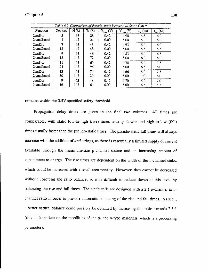
Chapter 6 130
Table 6.2. Comvarison of Pseudo-static Versus Full Static CMOS Function Devices H (/...) w (/...) v~.- (V) VH.. (V) tp. (ns) tp., (ns)
2andlor 5 63 28 0.42 4.90 4.5 6.0 2nand1nand 4 147 24 0.00 5.00 5.0 5.0 2and2or 7 63 43 0.42 4.93 5.0 6.0 2nand2nand 12 147 48 0.00 5.00 5.5 5.5 2and3or 9 63 46 0.42 4.83 5.0 6.5 2nand3nand 18 147 72 0.00 5.00 6.0 6.0 2and4or 11 63 60 0.42 4.70 5.0 7.5 2nand4nand 24 147 96 0.00 5.00 6.5 6.0 2and5or 13 63 74 0.42 4.66 5.0 7.5 2nand5nand 30 147 120 0.00 5.00 7.0 6.0 3and2or 9 63 48 0.47 4.70 5.0 7.0 3nand2nand 16 147 64 0.00 5.00 6.5 5.5
remains within the 0.5V specified safety threshold.
Propagation delay times are given in the final two columns. All times are
comparable, with static low-to-high (rise) times usually slower and high-to-low (fall)
times usually faster than the pseudo-static times. The pseudo-static fall times will always
increase with the addition of and strings, as there is essentially a limited supply of current
available through the minimum-size p-channel source and an increasing amount of
capacitance to charge. The rise times are dependent on the width of the n-channel sinks,
which could be increased with a small area penalty. However, they cannot be decreased
without upsetting the ratio balance, so it is difficult to reduce skews at this level by
balancing the rise and fall times. The static cells are designed with a 2:1 p-channel to n-
channel ratio in order to provide automatic balancing of the rise and fall times. As seen,
a better natural balance could possibly be obtained by increasing this ratio towards 2.5:1
(this is dependent on the mobilities of the p- and n-type materials, which is a processing
parameter).
Chapter 6 131
To allow an even greater noise margin, specifying a safety threshold of 0.25V
would have involved increasing the n-channel sizes such that a ratio of 12.44:4 is
maintained between the n-channel width and the minimum-size p-channel width.
However, this would also have served to increase the charge-sharing problem, as
increasing the n-channel width increases the amount of capacitance in the and strings
available for charge sharing. This could then be alleviated by increasing the size of the
pre-charge node, possibly by increasing the size of the output inverter associated with
this implementation and thus increasing its input gate capacitance. However, this also
has its penalty, as increasing the size of the pre-charge node increases the circuit delay.
Much more detailed circuit simulation becomes necessary to guarantee proper operation
of the pseudo-static scheme for different circuit configurations, thus requiring
significantly more design time.
The third control implementation option to be considered is dynamic CMOS
[Kram82] [Gonc83] [Lee86]. While the previous two design styles did not require any
clocking, dynamic techniques do require at least one clock signal. The scheme
essentially consists in precharging a node, and then conditionally discharging it
depending on the inputs. There are two main problems with dynamic design -- charge
redistribution and clock skew. Charge redistribution occurs when the charge on the
output node is transferred to some of the internal nodes of the circuit [Pret86]. For the
circuit to work, a reduced 'high' level on the precharge node should still be higher than
the logic threshold of the output inverter. This is illustrated in Figure 6.9.
The second problem with dynamic circuits is clock skew [Oklo85]. Even though
two logic blocks get the same clock signal, physically the clock signals can be different if
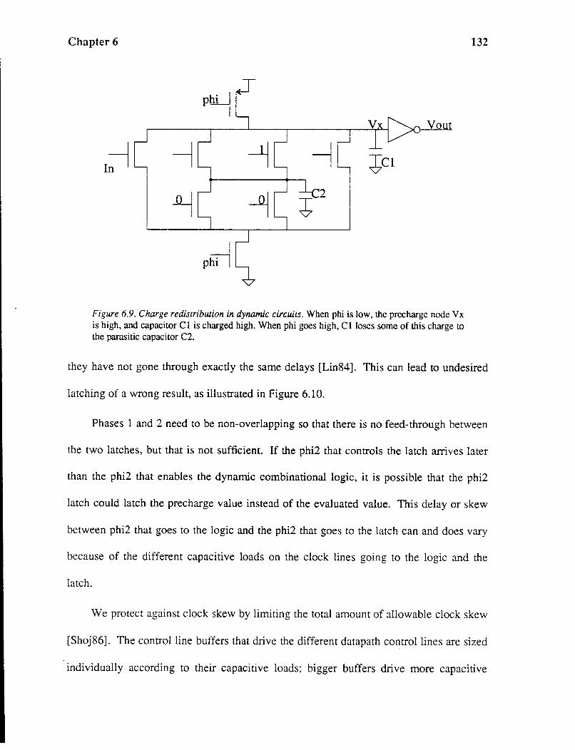
Chapter 6
I~
Figure 6.9. Charge redistribution in dynamic circuits. When phi is low, the precharge node Vx is high, and capacitor Cl is charged high. When phi goes high, Cl loses some of this charge to the parasitic capacitor C2.
132
they have not gone through exactly the same delays [Lin84]. This can lead to undesired
latching of a wrong result, as illustrated in Figure 6.10.
Phases 1 and 2 need to be non-overlapping so that there is no feed-through between
the two latches, but that is not sufficient. If the phi2 that controls the latch arrives later
than the phi2 that enables the dynamic combinational logic, it is possible that the phi2
latch could latch the precharge value instead of the evaluated value. This delay or skew
between phi2 that goes to the logic and the phi2 that goes to the latch can and does vary
because of the different capacitive loads on the clock lines going to the logic and the
latch.
We protect against clock skew by limiting the total amount of allowable clock skew
[Shoj86]. The control line buffers that drive the different datapath control lines are sized
individually according to their capacitive loads; bigger buffers drive more capacitive
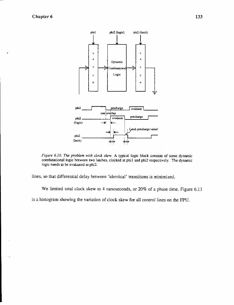
Chapter 6
phil phi2 (logic) phi2 (latch)
L L
A A
Dynamic
T T
c Logic c
H H
phil __j precharge I evaluate ._l __ _
I ' non~v~rlap
phi2 1! i-e..:v_al-ua_te..,l precharge r-----------~~1 :
(logic) ~ +--. !
Phi2
~. *-- ~ )Ytch precharge value!
--------~i :\_ r-(latch) ++ s~+
Figure 6.10. The problem with clock skew. A typical logic block consists of some dynamic combinational logic between two latches, clocked at phil and phi2 respectively. The dynamic logic needs to be evaluated at phi2.
lines, so that differential delay between 'identical' transitions is minimized.
133
We limited total clock skew to 4 nanoseconds, or 20% of a phase time. Figure 6.11
is a histogram showing the variation of clock skew for all control lines on the FPU.
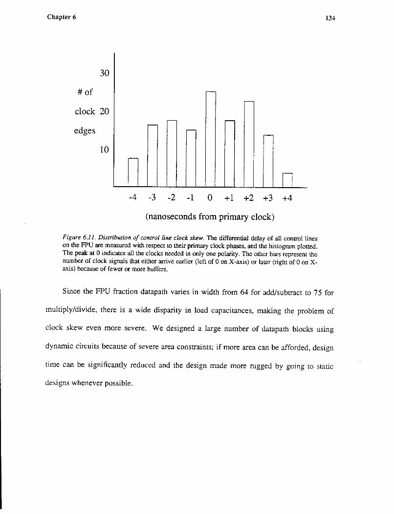
Chapter 6
30
#of ..---r--
clock 20 - r--
-r--
r--edges
10 -
n -4 -3 -2 -1 0 +1 +2 +3 +4
(nanoseconds from primary clock)
Figure 6.11. Distribution of control line clock skew. The differential delay of all control lines on the FPU are measured with respect to their primary clock phases, and the histogram plotted. The peak at 0 indicates all the clocks needed in only one polarity. The other bars represent the number of clock signals that either arrive earlier (left of 0 on X-axis) or later (right of 0 on Xaxis) because of fewer or more buffers.
134
Since the FPU fraction datapath varies in width from 64 for add/subtract to 75 for
multiply/divide, there is a wide disparity in load capacitances, making the problem of
clock skew even more severe. We designed a large number of datapath blocks using
dynamic circuits because of severe area constraints; if more area can be afforded, design
time can be significantly reduced and the design made more rugged by going to static
designs whenever possible.

Chapter 6 135
6.6. Summary
The design of the components of the SPUR FPU control unit are presented first in
this chapter, to form a basis for discussion of major performance limiting factors.
Instruction decoding, a pipeline for Load and Store operations, and the arithmetic control
unit, including the state machine and the cycle counter are discussed.
The basis for partitioning control into separate PLAs is discussed next. Here again,
area-time tradeoffs have to be investigated to determine the optimum mix of inputs and
outputs between different PLAs. In the case of SPUR, the central control was partitioned
into three PLAs with delays within 10% of each other and all less than one phase time, so
that control logic close to the datapath -- the second level of control -- had time to
complete evaluation within the allotted phase.
Circuit design options for control circuits are discussed next. Two static schemes
are compared for area, delay, and noise margin, for a variety of gates. Full static CMOS
provides a greater speed advantage than the pseudo-static design at the cost of extra area,
but is a safer design, because of its higher noise immunity, and has the added advantage
of not requiring any DC power. The impact of datapath design styles on control unit
design is explored.
Two of the main problems of dynamic circuit design -- charge redistribution and
clock skew -- are investigated next. Both problems, especially clock skew, could
potentially limit performance improvements with scaling technology. Ways of
minimizing clock skew are presented, and careful sizing of control line buffers to match
control line capacitance is shown to limit differential clock delays to within a small
percentage of processor cycle time.

....... '-""''.
Chapter 6 136
Jensen [Jens87] helped with the layout and circuit simulation of some control
components.

Chapter 6 137
6.7. References
[Gonc83] N. Goncalves and H. DeMan, NORA: A Racefree Dynamic CMOS Technique for Pipelined Logic Structures, IEEE Journal of Solid-State Circuits, Vol. SC-18, No.3 (June 1983), pp. 261-266.
[Jens87] D. Jensen, Control Implementation for the SPUR Floating Point Coprocessor, Computer Science Division (EECS) Report No. UCB/CSD 87/369, University of California, Berkeley (August 24, 1987).
[Jeon87] D. Jeong, G. Borriello, D. A. Hodges and R. H. Katz, Design of PLL-Based Clock Generation Circuits, IEEE Journal of Solid-State Circuits, Vol. SC-22, No.2 (April1987), pp. 255-261.
[Kram82] R. Krambeck, C. Lee and H. Law, High-Speed Compact Circuits with CMOS, IEEE Journal of Solid-State Circuits, Vol. SC-17, No. 3 (June 1982), pp. 614-619.
[Lee86] C. M. Lee and E. W. Szeto, Zipper CMOS, IEEE Circuits and Devices(May 1986), pp. 10-17.
[Lin84] T. Lin and C. Mead, Signal Delay in General RC Networks, IEEE Transactions on CAD of Integrated Circuits and Systems, Vol. CAD-3, No.4 (October 1984), pp. 331-349.
[Oklo85] V. J. Oklobdzija and R. K. Montoye, Design-Performance Trade-offs in CMOS Domino Logic, Proc. IEEE Int' !. Custom !.C. Conf(May, 1985).
[Pret86] J. A. Pretorius, A. S. Shubat and C. A. T. Salama, Charge Redistribution and noise margins in Domino CMOS Logic, IEEE Transactions on Circuits and Systems, Vol. CAS-33 (August 1986), pp. 786-793.
[Shoj86] M. Shoji, Elimination of Process-Dependent Clock Skew in CMOS VLSI, IEEE Journal of Solid-State Circuits, Vol. SC-21, No. 5 (October 1986), pp. 875-880.
7 Implications of Scaling Technology
138
This chapter discusses the effects of technology scaling on floating-point
computation. Perhaps the single most dominant factor in the performance improvement
of processors in recent years has been the evolution of technology towards finer
geometries. This trend has shown no sign of diminishing, and is expected to continue at
around this rate, for about the next ten years. This has allowed the individual transistors
to get faster and smaller, with more transistors fitting on a single chip, which itself is also
getting larger. This trend has continued unabated since the early 1970's, with minimum
line-widths decreasing from around eight microns in 1972 to around one micron in 1988 .
. Chip sizes have gone up from 10 sq.mm. to 100 sq.mm., and the number of transistors

Chapter 7 139
from 1,000 to 250,000 for processors and 10,000 to 4 million for memories [Myer86]
[Asai86]. The effects of scaling are pervasive across all levels of processor design, and
we shall look at all of them in turn, from devices and circuits, through logic and micro-
architecture, to algorithms and system architecture.
7.1. Scaling at the Device/Circuit Level
Classical, or constant-field scaling, [Denn74] attempts to scale all dimensions of a
technology, all device voltages, and all concentration densities by the same factor a. The
effect of this scaling on device and circuit parameters is shown in Table 7 .1.
Table 7.1: Effect of classical scalin on device and circuit parameters. Device Parameters Circuit Parameters
Parameter Scale Factor Parameter Scale Factor Length, Width 1/a Parasitic Capacitance 1/a Gate Oxide Thickness 1/a Gate Area l/a2
Supply Voltage 1/a Gate Delay 1/a Junction Depth 1/a Power Dissipation l/a2
Depletion Layer 1/a Power-Delay Product 1/a3
Substrate Doping a Current Density a
As device parameters are scaled by a constant factor a, circuit area, delay and power-delay product increase significantly. Note that substrate doping and current density increase with scaling, ultimately becoming some of the limiting factors.
We see that reducing the feature size by a causes area to decrease by the square of
a and the speed to increase by the same factor. But scaling cannot go on indefinitely,
and junction and oxide breakdown at high electric fields limit the extent of scaling.
Again, the problem of increasing sub-threshold conduction makes it difficult to reduce
transistor threshold voltages much below 0.6 volt. This militates against the
proportionate scaling of the power supply voltage, leading to a slower decrease in the
power supply voltage compared to the decrease in line widths. When scaling with
Chapter7 140
constant power supply voltage, the gate delays decrease by the square of a (instead of a
for classical scaling), but the power dissipation increases by a, leading to power-delay
product that decreases at the rate of 1/a, which is less dramatic than that for classical
scaling.
Deviations from classical scaling have to be made in several instances, as we
approach sub-micron dimensions [Labo82] [Take85]. One such case is that of
interconnect resistance. With classical scaling, the delay time of local interconnects
remains the same since line resistance increases by a, while line capacitance decreases
by a, keeping the RC delay constant. The delay for long interconnects actually
increases, while the delay time of transistors decreases by a. One way to keep
interconnect resistances small is to scale down interconnect thicknesses at a rate smaller
than a. Interconnect density, though, has improved rapidly over the last few years, with
reductions in metal and polysilicon pitch, and the availability of second and third metal
layers. This should help solve some of the communication bottlenecks when multiple
sub-systems are integrated on the same chip.
Other concerns at sub-micron device sizes include mobility degradation, increased
susceptibility to latch-up, increased leakage current, reduced noise immunity, increased
power dissipation at higher frequencies, and an increase in the ratio of wiring capacitance
to device capacitance.
Mobility degradation will not allow speed improvements to continue at the rate
predicted by classical scaling. Even with constant electric fields within the transistor,
intrinsic material properties will limit performance enhancement, limiting gains in device
transconductance and hence speed. Other short-channel effects like drain-induced barrier
Chapter 7 141
lowering will also ultimately limit scaling [Pfie85]. Increased sub-threshold leakage
currents, together with decrease in device and interconnect capacitance, will determine
the scaling limits of dynamic CMOS circuits, while static CMOS circuits will be limited
by noise immunity degradation caused by short-channel effects.
7 .2. Scaling at the LogidMicro-architectural Level
The principal challenge at this level will be the design and implementation of clock
distribution systems [Ance82] [Frie86]. At sub-micron geometries, it is conceivable that
there will be several million transistors on a single chip, and ensuring proper
synchronization between different parts of the chip will require significant effort.
One of the approaches that can be extrapolated down from multi-board-level design
is the notion of independent modules on a single chip, interconnected by a synchronous
communication mechanism. This avoids a key problem of the self-timed approach,
where there is no unique time reference; also, the same clocking design philosophy used
in the design of individual circuits and sub-modules, can be extended to the entire chip.
Different modules within the chip, each possibly containing 100,000 transistors,
could be considered isochronic: that is, they would have an identical time reference
throughout the region of the module, much like an equipotential region, as shown in
Figure 7.1.
Once the entire chip is partitioned into separate isochronic regions, the individual
module clocks will have to be synchronized to the master clock generator. This can be
done using phase-locked-loops (PLLs), as shown in Figure 7.2.
Chapter7
!Or-----------------------------------~ mm
5
0 5 !Omm
Figure 7.1. Isochronic Regions on a Single VLSI Chip. The size of each region depends on the circuit density and capacitive loading on clock lines. Each isochronic region, e.g. multiplier array or high-radix divider, is driven by its own clock, with maximum clock skew in an entire region held below some fraction of the clock period.
r_ o 1 Oock Broadcast Oock
Gen.
'itp Divide
Module Module byN Module Oock
Communication l I T Oock
Communication Bus
Figure 7.2. Clock Distribution between Modules. Communication between modules is synchronized to the communication clock, which is derived from the crystal clock generator. Since driver and wire delays are there in each module, the communication clock can be slower than the broadcast clock.
142
Chapter 7 143
We have seen how classical scaling can lead to proportionate increase in wire delay
-- while gate delay decreases, wire delay remains constant -- but even if interconnect
scaling occurs at a slower rate than gate lengths, communication delay will be
increasingly important in determining total delay. Meta-stability may be avoided by
maintaining correct phase relationship between the communication clock and the
broadcast clock. Phase-locked-loops (PLLs) are needed in each module, to ensure
synchronization between each internal module clock and the communication clock, to
maintain a synchronous communication interface between modules. The PLLs need not
be very accurate, as long as they are able to compensate for process variations and
temperature effects on propagation delay.
7.3. Scaling and Arithmetic Algorithms
Further enhancements in algorithm performance will come from two inter-related
factors. First, as technology continues to scale to smaller geometries, individual
transistors and logic gates will improve in performance. Second, for the same total chip
area, scaling will also allow more logic on a single chip. This will allow designers to go
to faster algorithms and get even greater speed-up than that achievable by simply scaling
technology. Figure 7.3 shows the effect of scaling a floating-point unit from 2 microns to
1 micron and 0.5 micron, leading to about a 400% increase in device density at 1 micron.
For addition and subtraction, individual components of the datapath, like the adder
and shifter, will speed up as technology scales. An optimization can be added to the
add/subtract datapath to distinguish between two mutually exclusive cases: a long
alignment right shift and a long normalizing left shift to the fraction. Normalizing
Chapter 7
10~----------------------------~ mm
5
0 5 !Omm
Figure 7.3. Impact of scaling the FPU from 2J.L to 05J.L. The FPU, as presently designed, is reduced to approximately a fourth its present size when the technology scales from two to 1 micron, and to about 6% its present size at 0.5 micron, freeing up 75% to 94% of the chip area at lJ.l. and 0.5J.L respectively.
144
implies possibly long left shifts of the intermediate result, while rounding implies that the
intermediate result gets no shift at all or at most a shift of one bit right or left, depending
on whether the number is greater or less than unity. Of course it is quite possible that
neither a long right shift or a long left shift are necessary. The mutually exclusive long-
shift conditions can be summarized as follows:
If 0~ R-Shift ~;;],then
a) when normalizing, :Q L-Shift ~63 or
b) when rounding, L-Shift ~1
If ~2 R-Shift ~67, then
definitely going to round, and L-Shift ~1
Chapter 7 145
It turns out that if the exponent difference indicates that a long alignment right shift
is necessary, the datapath effectively looks like a right shifter followed by an adder. On
the other hand, if the exponents are close, the long alignment right shift is not necessary,
and the datapath could look like an adder followed by a left shifter. It is thus possible,
with a little extra control, to eliminate one shifter delay from the add/subtract critical
path.
Going from 2 micron to 1 micron technology, large combinational multipliers will
become feasible as components in an FPU, requiring area comparable to the SPUR FPU
multiplier, as seen in Figure 7.4. A 64 x 32 array multiplier in 1 micron technology
should take about 60% of the area of the present multiplier area; a 64 x 64 array
multiplier in 1 micron technology should be about the same size as the iterative SPUR
multiplier, while providing about a lOx speed improvement.
Dividers, being inherently sequential in nature, are harder to speed up. The
escalating area and time cost in the quotient selection logic will probably limit the use of
non-restoring divide to radix 16 [Tayl85]. The area needed for partial remainder
evaluation will be virtually unaffected, but the quotient selection logic will increase from
radix 4 by about 6 times. Prescaling schemes [Erce85], to generate more quotient bits
per iteration, are worth exploring. Eight and even sixteen bits per iteration seem feasible,
provided that initial setup, final remainder adjustment, and data flow can be handled
efficiently. Figure 7.5 shows algorithmic options for divide with changing technology.
The estimate for prescaling in Figure 7.5 takes into account two 64 x 8 multipliers, and
the increase in datapath width by eight bits; on the other hand, quotient selection logic is
greatly simplified.

Chapter 7
------------·----------------------------------··-·-----·----·--------------·-----···----···---------.. . . ! Multiply Algorithm Area-Time Cost i Area
4
Area 0 2 micron
~ 1 micron
3 ·····················································-······t······+·········· Time [] 2 micron
I 1 micron Area 2 f···································=-~~~~: ............................. , .......... .
0 ~~~~~~--~~~~~--~~~~~--
Multiply Multiply Multiply 64*8 64*32 64*64
~--·----------·······:~~-~~---·····--·------···--~~~---·-----····------~~:. ••••••••••••••••. 1
Figure 7.4. Multiply Algorithm Area-Time Cost. Area and time are normalized to those for our implementation in 2 micron CMOS. For example, our multiply scheme will be 25% its present size when built in 1 micron CMOS and will be 4 times as fast.
146
High radix prescale dividers should become feasible as technology scales from 2
micron to 1 micron. A radix 256 prescale divider in 1 micron CMOS, occupying about
the same area as a radix-4 SRT divider in 2 micron CMOS, could provide an order of
magnitude speed improvement, combining the effects of faster technology and faster
algorithms.
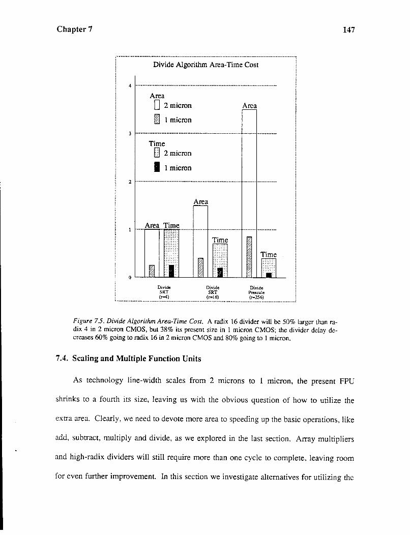
Chapter 7
-------------------·---------···-----------------------------------··-------------------·--------------- .. ' ' ' ' i Divide Algorithm Area-Time Cost i
4 ----------------------------------------------------------------------------------
Area D 2 micron Area
~ 1 micron
3 ------------------------- ------------------------------------ ------- -----------
Time [l 2 micron
I 1 micron
2 ------------------------------------------------------------- ------- -----------
Area Time
Divide SRT (1'24)
Area
Divide SRT
(1'216)
Divide Prescale (r=256)
'
--------------------------------------------------------------------------------------------------------
Figure 7 5. Divide Algorithm Area-Time Cost. A radix 16 divider will be 50% larger than radix 4 in 2 micron CMOS, but 38% its present size in 1 micron CMOS; the divider delay decreases 60% going to radix 16 in 2 micron CMOS and 80% going to 1 micron.
7.4. Scaling and Multiple Function Units
147
As technology line-width scales from 2 microns to 1 micron, the present FPU
shrinks to a fourth its size, leaving us with the obvious question of how to utilize the
extra area. Clearly, we need to devote more area to speeding up the basic operations, like
add, subtract, multiply and divide, as we explored in the last section. Array multipliers
and high-radix dividers will still require more than one cycle to complete, leaving room
for even further improvement In this section we investigate alternatives for utilizing the

Chapter 7 148
increased device density to achieve even higher throughput.
Presently, most FPUs share the add/subtract fraction unit's components, including
the shifter, adder and rounding logic, for different instructions. For higher performance
and increased parallelism, these components could be duplicated, so that the different
arithmetic units can be independent. Keeping these functional units independent, and
with a multi-port on-chip register file, it should be possible to begin execution of multiple
arithmetic operations simultaneous! y. Figure 7. 6 shows the interaction of different
function units in such a system.
Instr
Control Decode
I .___, Add/Subtract Unit 1 r-
~ Add/Subtract Unit 2 r--l/0 Register Arith ~
Data Control File Control ~ Multiply Unit i4-----
~ Divide Unit ~
Figure 7.6. Increased parallelism with independent function units. The register file has multiple ports, so that it can service all four independent functions, for add/subtract, multiply and divide. Two add/subtract units are shown, to balance operation frequencies (see Ch.2). In addition, the architecture remains decoupled, so that I/0 and arithmetic can proceed independently and simultaneously.
There are several design alternatives to take advantage of parallelism between
different function units. The individual operations may be pipelined to improve
performance, with nominal increase in hardware. A logical sequence of pipeline stages
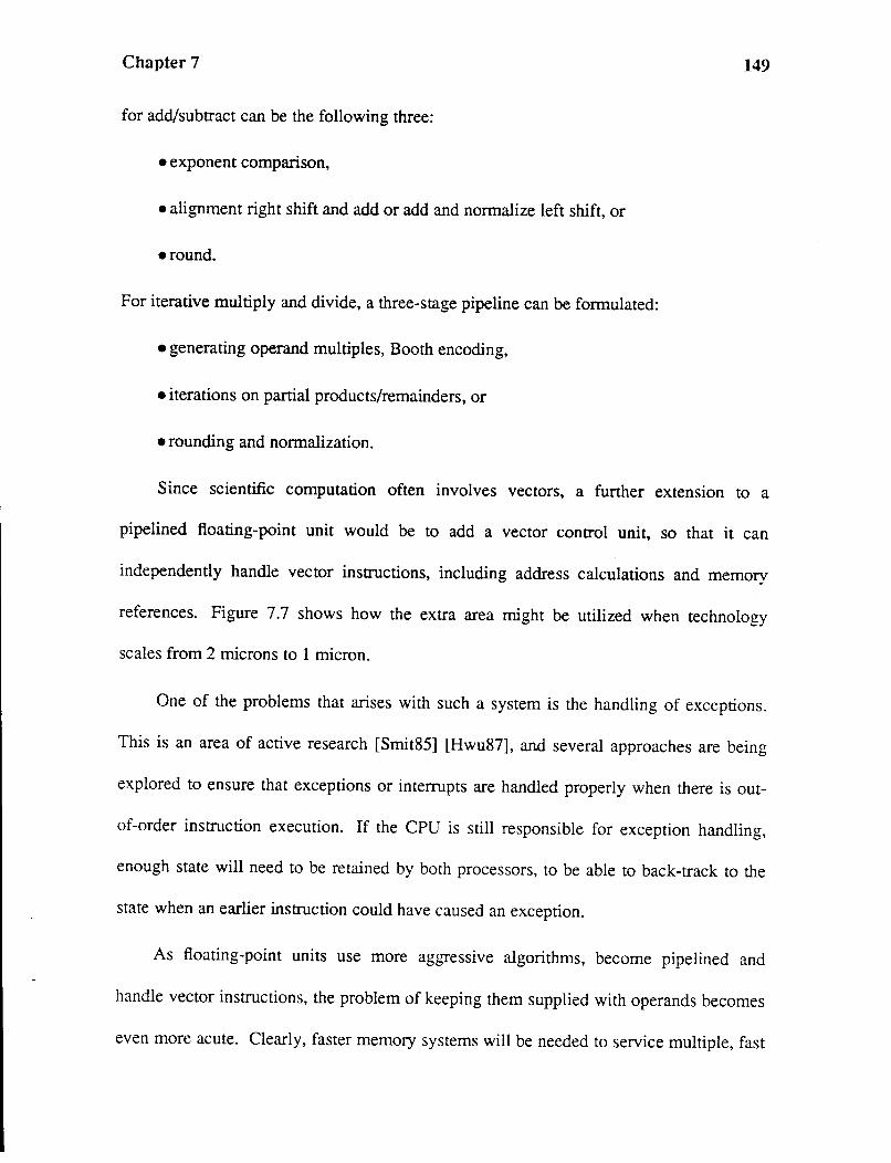
Chapter 7
for add/subtract can be the following three:
• exponent comparison,
• alignment right shift and add or add and normalize left shift, or
•round.
For iterative multiply and divide, a three-stage pipeline can be formulated:
• generating operand multiples, Booth encoding,
• iterations on partial products/remainders, or
• rounding and normalization.
149
Since scientific computation often involves vectors, a further extension to a
pipelined floating-point unit would be to add a vector control unit, so that it can
independently handle vector instructions, including address calculations and memory
references. Figure 7.7 shows how the extra area might be utilized when technology
scales from 2 microns to 1 micron.
One of the problems that arises with such a system is the handling of exceptions.
This is an area of active research [Smit85] [Hwu87], and several approaches are being
explored to ensure that exceptions or interrupts are handled properly when there is out
of-order instruction execution. If the CPU is still responsible for exception handling,
enough state will need to be retained by both processors, to be able to back-track to the
state when an earlier instruction could have caused an exception.
As floating-point units use more aggressive algorithms, become pipelined and
handle vector instructions, the problem of keeping them supplied with operands becomes
even more acute. Clearly, faster memory systems will be needed to service multiple, fast
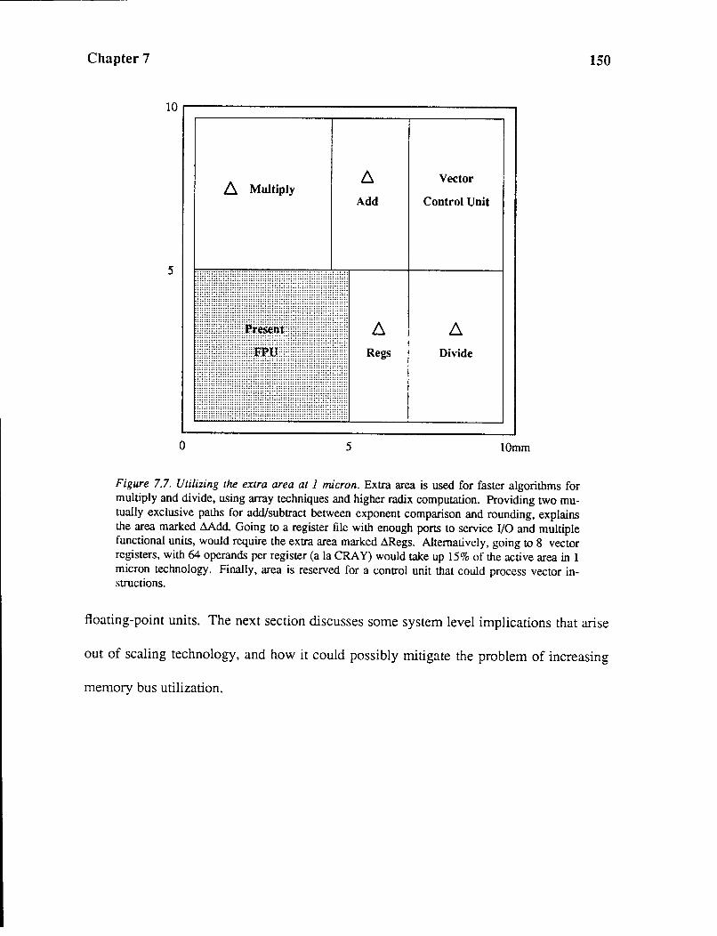
Chapter 7
10~--------------------------------------~
!J. Multiply
5
0 5
Add
Vector
Control Unit
Regs Divide
10mm
Figure 7.7. Utilizing the extra area at 1 micron. Extra area is used for faster algorithms for multiply and divide, using array techniques and higher radix computation. Providing two mutually exclusive paths for add/subtract between exponent comparison and rounding, explains the area marked LlAdd. Going to a register file with enough ports to service l/0 and multiple functional units, would require the extra area marked LlR.egs. Alternatively, going to 8 vector registers, with 64 operands per register (ala CRA Y) would take up 15% of the active area in 1 micron technology. Finally, area is reserved for a control unit that could process vector instructions.
150
floating-point units. The next section discusses some system level implications that arise
out of scaling technology, and how it could possibly mitigate the problem of increasing
memory bus utilization.

Chapter 7 151
7.5. Scaling at the Architectural Level
Recall from Chapter 3 that one of the three components of overhead in a
coprocessor interface is the cache overhead. Cache access overhead becomes the major
component of communication overhead with a fast FPU. The problem worsens as
floating-point units improve in speed and optimizing compilers take advantage of
different forms of available concurrency and generate more efficient code. A very
aggressive, fully pipelined FPU architecture would nominally require one floating-point
operation started each cycle. This presumes some form of DMA between the cache and
the FPU to keep the FPU supplied with operands. The cache miss overhead will
probably not scale with technology, getting further compounded when multiple
processors share memory over a common bus. Figure 7. 8 shows the effects of various
FPU operation speeds and cache service times on system saturation -- the number of
processors that lead to 100% memory bus utilization -- for the program DP and LL5,
kernel 5 of the Livermore Loops from Chapter 2. For the same cache miss overhead, the
system saturates with fewer processors as FPU speed increases. As technology and
algorithms provide us with faster floating-point execution, the requirements on the
memory system for a shared-bus multiprocessor become even more critical. It is also
evident from Figure 7.8 that going to a faster memory system with half the cache service
time increases system saturation, allowing more processors to be connected to the
system, with commensurate net speed-up [Bose88].
One of the ways to reduce main memory accesses may be to integrate more of the
memory hierarchy with the processors. In the previous section, we outlined possibilities
for faster floating-point performance going from two micron technology to one micron
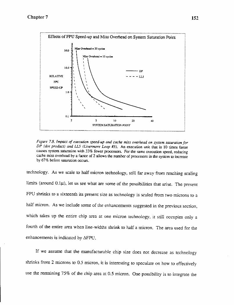
Chapter 7
1:·:.-------Eii~~~-~£-f;Fu-s~ct~~~-~ct--Mi~-~-o~~;h~~ct-~~-s-;~~~~-s-~~~~i~~-r;~i~~------···\
Mias Overhead • 20 cycles 50.0 I
10.0
Miss Overhead • 10 cycles I
I I
---DP
RELATIVE - - - - LL5
FPU
SPEED-UP
1.0
' ' 0.1 __________ _... _______ _
2 5 10 20 40
SYSTEM SATURATION POINT ' . ~-------------------------------····---------····---------·-·---------·-·------·---------------------------·----·----------------·---····--·-----·J
Figure 7.8. Impact of execution speed-up and cache miss overhead on system saturation for DP (dot product) and IL5 (Livermore Loop #5). An execution unit that is 10 times faster causes system saturation with 33% fewer processors. For the same execution speed, reducing cache miss overhead by a factor of 2 allows the number of processors in the system to increase by 67% before saturation occurs.
152
technology. As we scale to half micron technology, still far away from reaching scaling
limits (around 0.1~--L), let us see what are some of the possibilities that arise. The present
FPU shrinks to a sixteenth its present size as technology is scaled from two microns to a
half micron. As we include some of the enhancements suggested in the previous section,
which takes up the entire chip area at one micron technology, it still occupies only a
fourth of the entire area when line-widths shrink to half a micron. The area used for the
enhancements is indicated by .1FPU.
If we assume that the manufacturable chip size does not decrease as technology
shrinks from 2 microns to 0.5 micron, it is interesting to speculate on how to effectively
use the remaining 75% of the chip area at 0.5 micron. One possibility is to integrate the
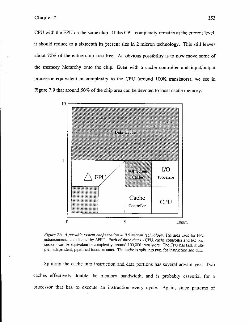
Chapter 7 153
CPU with the FPU on the same chip. If the CPU complexity remains at the current level,
it should reduce to a sixteenth its present size in 2 micron technology. This still leaves
about 70% of the entire chip area free. An obvious possibility is to now move some of
the memory hierarchy onto the chip. Even with a cache controller and input/output
processor equivalent in complexity to the CPU (around lOOK transistors), we see in
Figure 7.9 that around 50% of the chip area can be devoted to local cache memory.
5
I/0 Processor
Cache Controller
CPU
0 5 lOmm
Figure 7.9. A possible system configuration at 0.5 micron technology. The area used for FPU enhancements is indicated by Lif'PU. Each of three chips- CPU, cache controller and I/0 processor- can be equivalent in complexity, around 100,000 transistors. The FPU has fast, multiple, independent, pipelined function units. The cache is split into two, for instruction and data.
Splitting the cache into instruction and data portions has several advantages. Two
caches effectively double the memory bandwidth, and is probably essential for a
processor that has to execute an instruction every cycle. Again, since patterns of

Chapter 7 154
instruction and data references tend to be different, having two separate caches allows
independent, optimal choices of each cache's design parameters. One might even want
to split the data cache into two components, one servicing the integer CPU and the other
servicing the vector FPU, and the same would apply to the I/0 controller.
Extrapolating current memory cell sizes [Wada87] [Kimu87], it is conceivable that
the instruction cache can be 32KBytes of static RAM or 96KBytes of dynamic RAM;
and the size of the data cache can be 256KBytes of static RAM or 768KBytes of dynamic
RAM! Using the static RAM numbers for a SPUR-like system, but with a 64-bit bus and
sub-blocks, the miss ratio on the instruction cache could be reduced to less than 5%, and
the miss ratio on the data cache could be reduced to less than 1% [Hi1187].
7 .6. Summary
Technology scaling will continue steadily into the sub-micron region, leading to
denser, faster, larger chips. Technology scaling limits will be determined initially by
junction breakdown at high electric fields, and finally by quantum-mechanical tunneling,
around 0.1 micron. Special circuit techniques will need to be developed to counter
emerging problems with scaling, like increased power dissipation at higher frequencies,
lower noise margins, greater sensitivity to latch-up, and increased sub-threshold leakage
current.
System clocking will require careful design and implementation, if we are to take
advantage of integration in the range of 10 million transistors. Function modules, each
with around 100,000 transistors, may need to be have local clock generators, with local
phase-locked-loops providing the necessary tracking between modules, for synchronous

Chapter 7 155
communication.
Fast algorithms and their implementation and low overhead in communication are
both critical for high performance floating-point support in modern systems. Fast
algorithms for arithmetic and their implementation are discussed, in light of scaling
technology allowing higher levels of integration. It should soon be possible to integrate
multiple, pipelined function units on a single chip, providing an order of magnitude faster
execution with a factor of two scaling in technology.
The consequences of increasing memory bus utilization are investigated, especially
in light of faster floating-point processors. As floating-point computation speeds
increase, effective memory access times must also decrease to allow utilization of the
processors in the system. However, cache service times do not easily scale with
technology, and may become the bottleneck of future shared-memory multiprocessor
systems. Supporting fast scientific computation effectively with such systems may soon
require the design emphasis to shift from arithmetic algorithms to faster memory systems
to ensure that multiple, fast floating-point units remain compute-bound and not limited
by the memory. As technology scales from 2 microns to 0.5 micron, it may be possible
to integrate large instruction and data caches onto the same chip, together with integer
and floating-point processors.

Chapter 7 156
7. 7. References
[Ance82] F. Anceau, A Synchronous Approach for Clocking VLSI Systems, IEEE Journal of Solid-State Circuits, Vol. SC-17, No. 1 (February 1982), pp. 51-56.
[Asai86] S. Asai, Semiconductor Memory Trends, Proceedings of the IEEE, Vol. 74, No. 12 (December 1986), pp. 1623-1635.
[Bose88] B. K. Bose, P. M. Hansen, C. Lee and D. A. Patterson, Fast Scientific Computation in CMOS VLSI Shared-Memory Multiprocessors, Proc. IEEE Int'/ Symposium on Circuits and Systems(June, 1988), pp. 811-814.
[Denn74] R. H. Dennard, F. H. Gaensslen, L. Kuhn and H. N. Yu, Design of IonImplanted MOSFETs with very small physical dimensions, IEEE Journal of Solid-State Circuits, Vol. SC-9, No.5 (October 1974), pp. 256-268.
[Erce85] M. Ercegovac and T. Lang, A Division Algorithm with Prediction of Quotient Digits, Proc. Seventh IEEE Symposium on Computer Arithmetic(June 1985), pp. 51-56.
[Frie86] E. G. Friedman and S. Powell, Design and Analysis of a Hierarchical Clock Distribution System for Synchronous Standard Cell/Macrocell VLSI, IEEE Journal of Solid-State Circuits, Vol. SC-21, No.2 (April1986), pp. 240-246.
[Hill87] M. Hill, private communication (September 1987). [Hwu87] W. M. Hwu and Y. N. Patt, Checkpoint repair for High-Performance Out
of-Order Execution Machines, IEEE Transactions on Computers, Vol. C-36, No. 12 (December 1987), pp. 1496-1514.
[Kimu87] K. Kimura and K. Shimohigashi, A 65ns 4 Mbit CMOS DRAM with a Twisted Driveline Sense Amplifier, IEEE Journal of Solid State Circuits, Vol. SC-22, No.5 (October 1987), pp. 651-656.
[Labo82] V. Laboratory, Technology and Design Challenges of MOS VLSI, IEEE Journal of Solid-State Circuits, Vol. SC-17, No.3 (June 1982), pp. 442-448.
[Myer86] G. J. Myers, A. Y. C. Yu and D. L. House, Microprocessor Technology Trends, Proceedings of the IEEE, Vol. 74, No. 12 (December 1986), pp. 1605-1622.
[Pfie85] J. R. Pfiester, J. D. Shott and J. D. Meindl, Performance Limits of CMOS ULSI, IEEE Journal of Solid-State Circuits, Vol. SC-20, No. 1 (February 1985), pp. 253-263.
[Smit85] J. E. Smith and A. R. Pleszkun, Implementation of Precise Interrupts in Pipelined Processors, Proc. Twelfth Annual Symposium on Computer Architecture(June 1985), pp. 36-44.
[Tak:e85] E. Takeda, G. A. C. Jones and H. Ahmed, Constraints on the Application of 0.51J. MOSFETs to ULSI Systems, IEEE Journal of Solid-State Circuits, Vol. SC-20, No. 1 (February 1985), pp. 242-247.
[Tayl85] G. S. Taylor, Radix 16 SRT Division Methods With Overlapped Quotient Selection Stages, Proc. Seventh IEEE Symposium on Computer Arithmetic(June 1985), pp. 64-71.
Chapter 7 157
[Wada87] T. Wada and T. Hirose, A 34ns 1 Mbit CMOS SRAM Using Triple Polysilicon, IEEE Journal of Solid State Circuits, Vol. SC-22, No. 5 (October 1987), pp. 727-732.

158
8 Conclusions
This short chapter concludes this thesis with a recapitulation of the issues addressed
m the preceding chapters, emphasizing contributions in analysis and synthesis in the
present work. The chapter ends with recommendations for future work, suggesting
directions for further research that could enhance and extend the work reported here.
8.1. Summary
From a study of several computationally-intensive programs and program kernels
taken from a wide variety of real-world applications, the following common
characteristics emerge from static and dynamic measurements:
Chapter 8
• operands are mostly array elements, accessed in a regular arithmetic progression;
• most operations are simple, with add/subtract, multiply and divide being the most frequent;
• memory reads occur almost three times as often as memory writes, and the ratio of floating-point operations to memory references falls in a small range close to unity; and • there is scope for parallelism with floating-point operations at various levels, including integer computations and memory accesses.
159
From a comparison of several coprocessor interfaces, we find that the main
contributors to a high performance interface are: • a decoupled control and execution architecture allow data transfers to proceed while FPU functions are performed; • on-chip FPU register file and a wide data path between the memory and FPU minimize data transfer overhead; • an intelligent interface control unit allows FPU instruction decoding and execution in parallel with CPU instruction decoding and execution for maximum concurrency; and • implicit and explicit synchronization mechanisms provide the programmer complete control and flexibility.
The tradeoffs in implementing these features in hardware are discussed, and it is
shown that the increase in control complexity stems from maintaining decoupled control
units for memory and arithmetic operations. The datapath needs to support a wide bus --
at least 64 bits for extended precision, and requires a multi-port register file on chip to
accommodate I/0 parallelism.
The implications of hardware support for the IEEE standard are analyzed, and the
basis for partitioning tasks between hardware and software explored. It is found that it is
possible to delegate the evaluation of special functions and exception handling to
software, and implement the rest in hardware, while still retaining high performance.
Area versus time costs for different algorithms are compared, for the
implementation of the basic arithmetic functions. For a floating-point unit implemented

Chapter 8 160
on a single chip in 21J. CMOS technology, it is found that high-radix iterative techniques
work well for multiply, and significant hardware sharing occurs if implemented together
with iterative radix-4 SRT divide.
The very wide data-widths -- up to 75 bits -- in a floating-point unit fraction
datapath present unique challenges in logic and circuit design. Specific design details are
presented for all the area-intensive and time-critical datapath components in 2 micron
CMOS, including: a multi-ported 87-bit register file (for exponent and fraction) design
with access time of 17.7 nanoseconds; an optimized parallel-prefix 66-bit adder design
with carry computation of 25 nanoseconds; a 67 -bit bi-directional shifter and decoder
with embedded sticky bit generation, with a delay of 18.7 nanoseconds; and a compact
67-bit leading-one's detector that evaluates in 15 nanoseconds.
Techniques are developed for pipelining an iterative 64 x 8 multiplier to provide a
64 x 64 multiply in nine iterations, with two iterations per clock cycle. Effectively, the
inner loop provides the speed of a 64 x 16 multiplier, for significantly less area. The
design of a radix-4 SRT divider is presented, that computes the iterations for an extended
precision divide in 17 cycles. Even though two quotient bits are generated per iteration,
pipeline stages are overlapped to allow parallelism between quotient selection and partial
remainder formation, making it possible for four quotient bits to be generated every
cycle. Consequently, we have a divider that provides the speed of radix-16 division for
the area of only a radix-4 divider. Methods are outlined for the formation of the
rounding bits -- Guard, Round and Sticky -- for multiplication and division, that requires
minimal hardware without slowing down the iteration pipeline, and proceeds in parallel
with formation of the final product.
...
Chapter 8 161
Design details are presented for FPU control units, including instruction decoding,
pipelining Load/Store instructions, state machine and cycle counter, and tradeoffs in PLA
partitioning are discussed. Circuit design options and consequences in control unit
design are explored, and a method is outlined for limiting clock skew or differential
clock delay to within just 16% of processor cycle time.
Scaling technology provides smaller, faster transistors, allowing more logic to be
integrated onto a single chip. Floating-point unit speed-up will come from faster cycle
times as well as from the possibility of implementing faster algorithms on a chip. Large,
combinational multiplier arrays and high-radix prescale dividers look like promising
candidates for speeding up these functions. It should soon be possible to integrate
multiple, pipelined function units on a single chip, providing an order of magnitude faster
execution with a factor of two scaling in technology.
As floating-point computation speeds increase, effective memory access times must
also decrease to allow utilization of the processors in the system. However, cache
service times do not easily scale with technology, and may become the bottleneck of
future shared-memory multiprocessor systems. ·Supporting fast scientific computation
effectively with such systems may soon require the design emphasis to shift from
arithmetic algorithms to faster memory systems to ensure that multiple, fast floating
point units remain compute-bound and not limited by the memory. As technology scales
from 2 microns to 0.5 micron, it should be possible to integrate large instruction and data
caches onto the same chip, together with integer and floating-point processors. Projected
sizes of instruction and data caches using static RAM design in 0.5 micron technology
are 32KBytes and 256KBytes respectively.
Chapter 8 162
8.2. Future Work
The work reported in this thesis can be developed and extended in several
directions. As technology scales to smaller geometries, new circuit techniques will need
to be developed to counter the effects of speed-up less than proportionate to density
improvements. Operating circuits at lower temperatures [Hana85] and techniques for
suppressing hot carrier generation [Saku85] appear promising. Investigation of design
feasibility in other technologies, such as gallium arsenide, will become increasingly
important as MOS approaches the limits of scaling around 0.1 micron in about a decade.
Once again, area-time tradeoff analyses should help match the appropriate algorithms to
available technology.
Long before the limits of MOS VLSI scaling are reached, major design challenges
await us. In algorithms, much work remains in exploring fast algorithms for divide, with
possible extensions for square root. As multipliers are implemented with larger and
larger combinational arrays, division times are unable to keep pace and will have to be
speeded up. With more aggressive algorithms and higher device density, signal delay
between logic blocks will become an increasingly larger percentage of the signal delay
within blocks. This will require studies into alternative timing strategies [Wann83],
including hierarchical clock generation and distribution techniques that will allow large,
complex logic modules to run independently while being able to communicate
synchronously with each other [Beau85].
As floating-point processors get faster with independent function units that are
pipelined and possibly vectored, the problem of exceptions with out-of-order instruction
execution will have to be addressed, so that interrupts are precise and can be traced back
Chapter 8 163
to a known and retrievable processor state. System partitioning with millions of
available transistors on a single chip, or on multiple chips on a single wafer (Wafer Scale
Integration), is an open architectural issue. As arithmetic units get faster, demanding new
instructions every cycle, memory system design for fast scientific computation will be at
least as important as the design of the computation algorithms themselves [Weis84]
[Bose89].
Concomitant with higher levels of system integration, will be the need for more
sophisticated computer-aided design tools [Newt87] that can support design efforts
involving millions of transistors. Significant developments will be required in the areas
of simulation at the behavioral level, good silicon compilation with logic and timing
verification, with special emphasis on testability.
Chapter 8 164
8.3. References
[Beau85] J. Beausang and A. Albicki, A Method to Obtain an Optimal Clocking Scheme for a Digital System, Proceedings of ICCD(October 1985), pp. 68-72.
[Bose89] B. K. Bose, P. M. Hansen, C. Lee and D. A. Patterson, VLSI Multiprocessor/Memory Interactions for Scientific Computation, accepted for publication in Journal of Parallel and Distributed Computing(1989).
[Hana85] S. Hanamura, M. Aoki and T. Masuhara, Low Temperature CMOS 8x8b Multipliers with Sub IOns Speeds, Proceedings of ISSCC(February 1985), pp. 210-211.
[Newt87] A. R. Newton and A. L. San giovanni-Vincentelli, Computer-Aided Design for VLSI Circuits, IEEE Computer, Vol. 19, No.4 (Aprill987).
[Saku85] T. Sakurai, M. Kakumu and T. Iizuka, Hot-Carrier Suppressed VLSI with Submicron Geometry, Proceedings of ISSCC(February 1985), pp. 272-273.
[Wann83] D. F. Wann and M. A. Franklin, Asynchronous and Clocked Control Structures for VLSI-based interconnection networks, IEEE Transaction on Computers, Vol. C-32, No.3 (March 1983), pp. 284-293.
[Weis84] S. Weiss and J. E. Smith, Instruction Issue Logic in Pipelined Supercomputers, IEEE Transaction on Computers, Vol. C-33 (November 1984 ), pp. 1013-1022.
165
...
Appendices
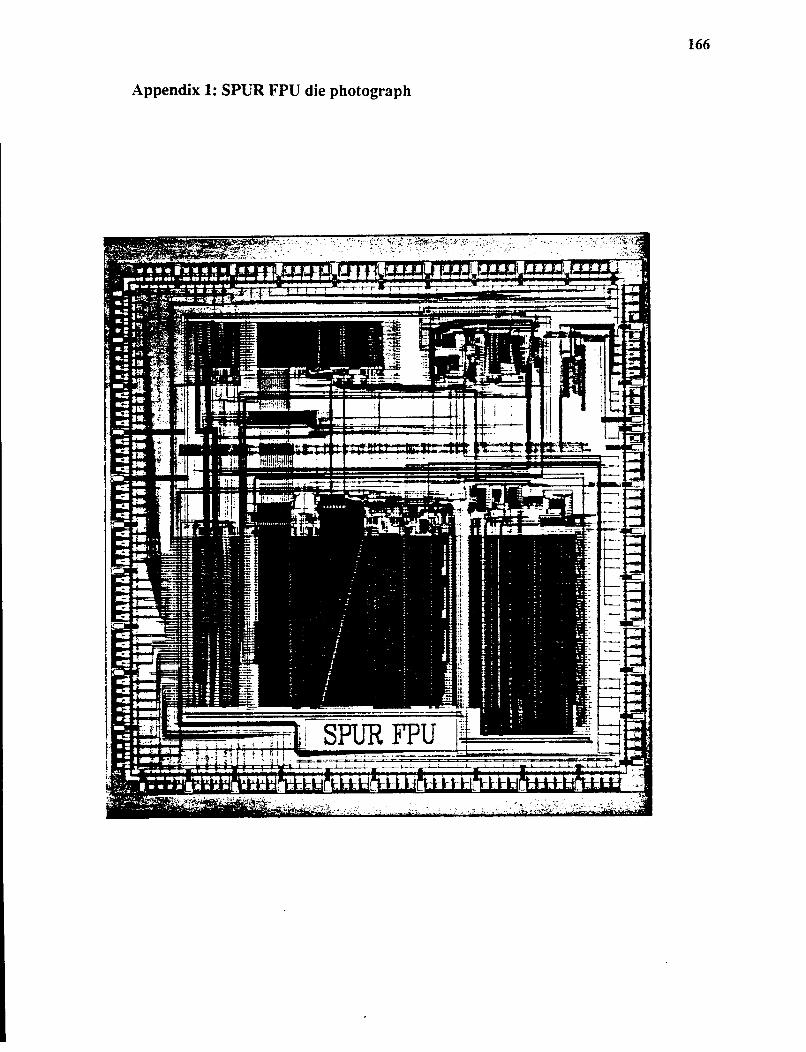
166
Appendix 1: SPUR FPU die photograph

167
Appendix 2: SPUR FPU Instruction Set and Cycle Times
Table A2.1: SPUR FPU Instruction Set and Cycle Times Instruction Instruction Semantics Latency in Cycles
FADD Rd,Rs1,Rs2 FPU Rd <-- FPU Rs1 + FPU Rs2 4 FSUB Rd,Rs1,Rs2 FPU Rd <-- FPU Rs1 - FPU Rs2 4 FMUL Rd,Rs1,Rs2 FPU Rd <-- FPU Rs1 x FPU Rs2 9 FDIV Rd,Rs1,Rs2 FPU Rd <-- FPU Rsl/ FPU Rs2 21 FMOV Rd,Rsl,O FPU Rd <-- FPU Rsl 4 FABS Rd,Rs1,0 FPU Rd <-- FPU Rs1, sign=O 4 FNEG Rd,Rs1,0 FPU Rd <-- FPU Rs1, sign complemented 4 FCMP cond,Rs 1 ,Rs2 FPSW <--result 4 CVTS Rd,Rs1,0 FPU Rd <-- FPU Rsl, convert to single 4 CVTD Rd,Rsl,O FPU Rd <-- FPU Rsl, convert to double 4 LD_SGL Rd,Rsl,RC FPU Rd <-- M[(Rsl+RC)] 4 LD_DBL Rd,Rs1,RC FPU Rd <-- M[(Rsl+RC)] 4 LD_EXTl Rd,Rsl,RC FPU Rd <-- M[(Rsl+RC)] 4 LD_EXT2 Rd,Rsl,RC FPU Rd <-- M[(Rsl+RC)] 4 ST_SGL Rs2,Rsl,RC FPU Rs2 --> M[(Rsl+RC)] 4 ST_DBL Rs2,Rsl,RC FPU Rs2 --> M[(Rsl+RC)] 4 ST_EXTI Rs2,Rsl,RC FPU Rs2 --> M[(Rsl+RC)] 4 ST EXT2 Rs2,Rsl,RC FPU Rs2 --> M[(Rs1+RC)] 4
The instructions are gathered into two groups -- arithmetic and memory. There is an implicit conversion to the common internal format on a Load, while explicit conversion is necessary on a Store. A cycle is 100 nanoseconds, and consists of four phases each 20 nanoseconds long and separated from the next by 5 nanoseconds. Arithmetic and memory operations may proceed simultaneously; back-to-back floating-point operations can overlap result write and next instruction fetch, effectively reducing the latency of each of the above instructions by one cycle.
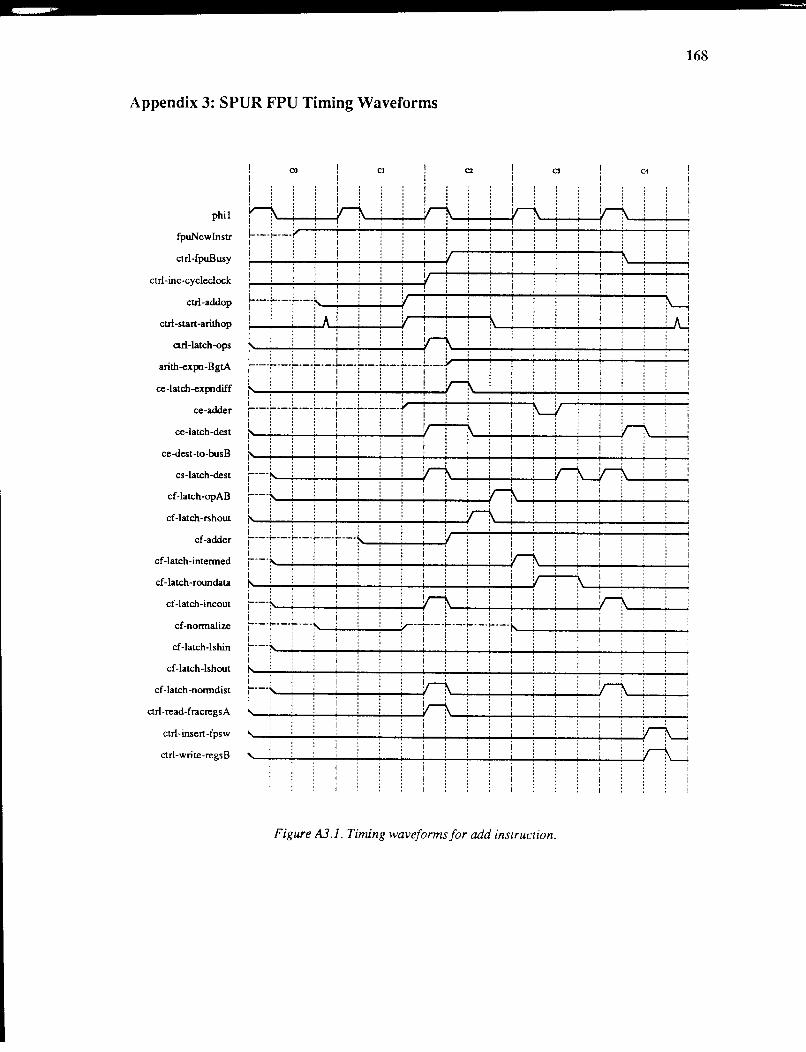
168
Appendix 3: SPUR FPU Timing Waveforms
phil
fpuNewinstr
ctrl-fpuBusy
ctrl-inc-cycleclock
ctrl-addop
ctrl-start -arithop
ctrl-latch-ops
arith-expn-BgtA
ce-latch-expndiff
ce-adder
ce-latch-dest
ce-dest-to-busB
cs-latch-dest
cf-latch-opAB
cf-latch-rshout
cf-adder
cf-latch-intenned
cf-latch-roundata
cf -latch-incout
cf-nonnalize
cf-latch-lshin
cf-latch-lshout
cf -latch -nonndist
ctrl-read-fracregsA
ctrl-insert-fpsw
ctrl-write-regsB
co Cl C2 C3 C4
L_ __ ;_ ___ :r----+~----+--i'-+--+---!--T--i----!---:--i--;.-o---:---1 I ' ' I
•i ••· :. i, y·.· ~ . .:''---;----;----; I I I -i i ~.vr~!---+--~--~~--~--+-_,~-+j--~--~~--~
r : 1 L--L-L--L .. :.v,.-;.!-+-+--+--+--~-+--:--;--+--+---i~.· : i I : : : ! :..__, ! ! ! ! " vr-+: --!---; i ~ ~ i i i r-r'-~~~~--~~~~~~~ i • · · I · • · I ,---:---:·--:---,---:·--:·--:---,---l i i i i l l i i ~: ;: I : : : i : : : i 1.....-i---+---f---i---+---~-i:---f--+--il L ___ [... ___ [... ___ [... ___ L_ __ [..._ __ [..._ __ ~r""""li~-+----+---~-t----i~.·.. : !.1 1 I : : : I : : i i'---f i 1 : : : i : ~,...._.____,\ !.:n.·. :1. ! ! i' : : : . : r ~'----!~-+---+--~--:---+~' : ~ i i i i i 11'---+--~--~-~~-~--~--;---~~----+---t--~--~--~--~--~~ i i !r-i. i i if"'i.:, I if"'i. :: ,---!" ... ---:~-+---+---+--:---:---off : ''-· ---:----:-: ---+i---:--f : ~ : ,..__.;.....___,; __ _, i ! i l--4 : : i : ,---:--'---~-+---;---+-~---+---+1--...;..--+, ---!( i\ i i i :
h ~ I ~ !--\~ ... ~--~--~--~~-~--+-___,;~_. ~--+--+--+--+---~ .... """"1~-+-----~i---?;:v : i i : : : i : i ir---\ ~---~ i 1 i i I f : ''-· ---"---+-~--.;......--;--_,______. i : : : i i ' i ~--~:--~:--~:--~~--~~--~~--~~--~~!~! ~:~~~--~~--~~ I : ! : i :
r---~~~i---+--~--,__~--~~v--\~-~---,__~~--~~ --+---~~~~~~--~ I i · · i i • · I i i, ~---;----:----~ :r·-r-·--:---; ---;-- --1'----i----i---+----"----:---i---~---'
~---! i i i i i i i i I
Figure AJ.l. Timing waveforms for add instruction.
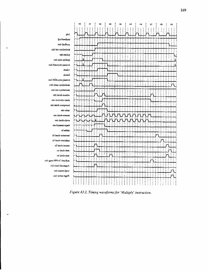
phil
fpu."<cwinstr
ctrl· fpuBusy
ctrl·inc-cycleclock
ctrl·mulop
ctrl-start-arithop
ctrl·firstcycle-passivc
clockl
clock2
ctrl-MDcycle-passivc
ctrl-clear-cyclcclock
ctrl-inc-cyclcclock
ctrl-latch-muldiv
ctrl-mul+div-latch
em·latch-compmcd
em-clear
em-latch-master
em-latch-slave
em-bytcscl·mpril
cf·adder
cf-latch-intcrmcd
cf-latch-roundata
cf-latch·incout
ce-latch·dcst
cs-latch-dcst
ctrl-gate·PPS+C-fracBus
ctrl-read·fracregsA
ctrl-insert·fpsw
ctrl-write-regsB
co Cl Cl C4 C6 C7 Cll
i : ' r+-~~-+~+-~-+~~~-+~~+-~-+~+-~-+~~~~~~-~-~-+~' ~~
i : : i : : ~ i ' : i I I • ' I • I • l i ~r1-~L~~ ~~,~~~~~~~~~-r~~~~~~~~~~. i I , , ii""TT"'7 I , , . il i : : ili : : rr:-n iAj I : : I ' I' : : : I : I H ili ~ I ; ; ! i l i1J ji !I ;ii,...W...W i t-~ i j j i , : : i ~ I
H !i i!iii!m-ti \ H il! ¥ i ' ' ' ' ~ i : i i I I I I ' I I • I I : I
I I i iihiihi i i fiJ i"""T"""! :'"'T'!""f :· I I : : I j i i i j i i i t : : : I : I I ' ' ' I ' ' ' !....l j !,...i : i, i-~ i i i i i i ~ J.j ~-i~....:-+-!-!-:..~~~+--!-!-+...:...lh'-~~....;...+-~-:..-ll ~~~-~-~-+~-~-W i i ~:· : i i::: i::: i:: H: I t i i i i i ; i i i i , ~ i l, i ~: : : i : i : i lr!-+-H i 1 ~ 1 ! i i ! ! i r : l ' ~ ! ; lJ.-U..LH.J.-· : . . . I : : : I : : : I : : I i-0-u-u-· j i i ' I j i: i I:: i.n--t-ti: : 1, 1, I I I I I I I I :rn-n-p· . 1 : • -+--;-.;.....,H--i-...:...+-~~-+-;-~~--i-~+-+-1 ~+-~-+-+-~! I : : : I : : : I ' ' ! j I r-::-:-r-w.J i i i 1
1:::1:::1 n·: .::.i H ; ~~ i i i i i 1 • • .... .... • -+-+-......,-+~-...... --...... +-~~--~r :''-+1 ~,.....,. _ _,_........,! l~~:+:~i~j~i+i~i~~~~~~~~~~~~~~~~i~~:. ···:.Y-~~1 ,~j iiI!! i i i ! , ~I! I i '' ·' '' ·' ~ :,' i, M!,: :. ; ·1 ~;, ! : I ! ! ! ' ~ I I ~ j , 1 t I I I I I :'-i-1 ""'11~-i--i-+-i-+-i--i--i-+-i-+-:-"1-+-i-i-r-i--i-~1 -t-~H1 : , · I ~: ·i:::m: i ili..L I : I, I : : • • I I : i i I
H I n: r.:. ruJj i : ; i :
n·.· .· ..... ~~~i~:.....;..: ...;.: ..... i 11 I j : . · j : : : i j i I j : j ~ i ! n .. i l : 1 i ! n .. i i 1 ! 1 1 ! r :'1
Figure A3.2. Timing waveforms for 'Multiply' instruction.
169

phil
fpuNewlnstr
ctrl-fpuBusy
ctrl-divop
ctrl-inc-cyc!eclock
ctr!-clear-cyclec!ock
ctrl- fi n;tcycle- passive
ctrl-MDcycle-passive
em-!atch-compmcd
an-clear
em-c!ear-div
em-latch-master
em-latch-slave
em-mux-dvr
ctrl-latch-muldiv
ctrl-mul+div-latch
ctrl-gate-PPS+C-fracBua
ctrl-gate-quotient-fracBus
ctrl-latch-remsign
cf-adder
cf-latch-intermed
cf-latch-roundata
cf-latch-incout
ce-latch-dcst
cs-latch-dcst
ctrl-read-fracregsA
ctrl-inscrt-fpsw
ctrl-write-regsB
170
i,,,i,,,l,,,l,,,l,,,l,,,l ,1,,,1,,,1,,,1,, 1,,,1,,,1 :' ':':1·':':':1· 1,,,1 ,,, I I I ""'Wtrrm"' . ........... ................ ......... . ... ~ .... . 1-:.:..:.1·: ..• _::1:::1:::1 :1:::1:::1:::1:: 1:::1:::1 ..... 1 ... 1 1:: :: :::1 i iiii: .. iiiii :!!1!!!1!:!1 11!!!1!!!1:!!1!: 1!!!1:::1 I! :I! ::1!!!1 1 .. 'i"· .. · riiiiiiijinjiiijiiijiiij jiiijiiijiiijii ji'ijiiij ii ijiiijiiij ;i~ i:::i:::,:::,:::,:::,:::, ,:::,:::,:::,:: ,: :,:::, ,: :i:::i:::i i!! i!;i:!!i! ~iiiilliiliiii:liiilil:·r iiiii'ilillli:i ii ;;;;;i il !i!ii!~~!! ''· '·'~ Wi iii i i Hi iii iii iii iii i i iii ii iii i iii i i iii iii i i : !: ; :! : i i! iii i i :: n:: i i~r .. , ... , ... , .. ' 1 ... .. , .. ,, .. '· ,, ... ,. !: .. , ... , ... , i:: i:::rM-H ili.i..l.iliJt1iiiiiil'iili i ilii iiiiliili ii iiiiii .. ,. iiilli:::i iii ililifW !iii!iiiWii!i~l: :,:: ,::: ::,:::,:: '.:: ::1.:::·.::1. ::1: :1::: I ::1 1:: I :::1::: I n.l.i..LLLLJl.l..i..W.Jli: iii\ dlil lli!llii! 1 11' 1 1" 1 ~:;: :;:::; ::; j:: j!!:f1.ilj li!iiiiihii!iiiii !iii iiiii iiiiiiiii iiiiiiiii iii !!iii! iii j:: iiiiiiiii ~~ ...... ,, .... :i::: ::;:::::: ;:::;:::; :;: ,j.,,j .. 1 ! .. ;:::i:::; i:: : i: :: i i:: i i i : i: : i: :: i i i i: i :: i: i: i : i i::: i i :: i : i : : i: :; i iii i:: i i i: i: iii I :::t: ::l:::t:::t: :t:::l :t:::t.::t:::l:: t:::t: ::1 ;,; ;,; ;; I ;;! 1:: 1 ... ,. ::-, i J J i j J J J j J J i j i i J j J J j J J J j i j J i i j i i J i i J i j J i j iii j iii j ; I; :I::; j ; :I j i J j J i J j i f\j iiiiiiiiiiiiiiiiii iii iii iiiiiliiiliiilii iiii iiiii iii iii iii iii iii i iiiiiii i !\\\i\\\i\\\i\\\i\ \i\\\i \!\\\i\\\i\\\i\\ !\\\!\\\! \!\ \\\\\! jjj i:: !\\:!\\\!
Figure A3.3. Timing waveforms for 'Divide' instruction.

phil
fpuNewlnstr
ctrl-fpuBusy
ctrl-inc-cycleclock
ctrl-cvtsop
clock 1-cvrtop
ctrl-start -arithop
ctrl-latch-ops
arith-expn-BgtA
ce-latch -expndiff
ce-adder
ce-latch-dest
ce-dest-to-busB
cs -latch -dest
cf-latch-opAB
cf -latch-rshout
cf-adder
cf -latch- in termed
cf-latch-roundata
cf-latch-incout
cf -normalize
cf-latch-lshin
cf-latch-lshout
cf -latch -norrndist
ctrl-read-fracregsA
ctrl-insert-fpsw
ctrl-write-regsB
co Ct C2 C3 C4
! I : : : . ,__._-;--+--+--i--+--+--i-_;.,--+--i--i' I r---:---:--t .... -~-~-_;_~r H i A i r. : : ~ .... -~--___. _ _,_....;..,.___. _ _,_-+-__,__~ !' ! v--r-.. i I : : : I : : j : i r----+----1---i---;---t---f---f----r-- :--' -+--i-+-+--i-+-+--+-+-+-~ i i i i i i ; ; i :.~ ·:.'--+--+-~--~~~~~~--+-~! " : : : i : : : I '! ~' I
~---~--L_L_i---\--- 1 __ J,..._._i -----~ . ._-!. __ .._~vr-_ ____._..._ _ ____. __ v-i i ! i ! i i
~--~~--+--+i--+--+--+--+i--~.~~'--+i--~-+--~-+--~-+--~~ ~---?- l h'--:-+. -+1 -..;....-:---;.-+--i---;.-..;....---i i ; i i ; ir--\ ~--""?' I i i ~ i''--i--i--+--i--i---i-----i
~'-~!~-+--!~~~~-~!~!~~~~~-~~-+~~~~~ ~---~--+---~---L-L"-i--+--+i.-~~:: r---:-+-+1 --+--:----+-+--:----+--+----t I : : : I : - i i_ : : : i : i ·n· i ---r- : : i : i i : : lL~:~-+-~i-+-~-+-r! ~-~~-ri--i~'--r-+--~+-~i 1- I I , I , : : j L_ : , ~~ i i i ;,.. I i --1' . . r 1""'....-_ __.__,.1_..;·-----· -----r '''-·....-,___.__ ... --II i----l----i---~""--~-..:..,_ ..... vr--~ ___.._.._-+----~ ~'----_,___,__. -+' _..__,___---;::~ i i : : : i i I , :--,
i----\ : : i i n : i j i I I : : : I .. ' ··~· 1, : I I : : : I j ! I ! I ' I I-' __ _;, : ~.. ',..--i, : : '
"' [I !\ V i\ i i I j i I i '----+-------:---+----4--~1 :, · ' I ~ i v--i\ I i I :'--~~--~--;-~--_;__~--__._--~. --~.~~ ' ' ' ir--X: :' ~ I : r :'---< ~~~---i--~--~~--+---+--41--~--i-~--~-+--~-i--~--;-~: : I ~~~~-+~--~~~~i--~+-~~-+-+~--~---~ I I ' : I i I i i I i i i
Figure A3.4. Timing waveforms for 'Convert (to) Single' instruction.
171
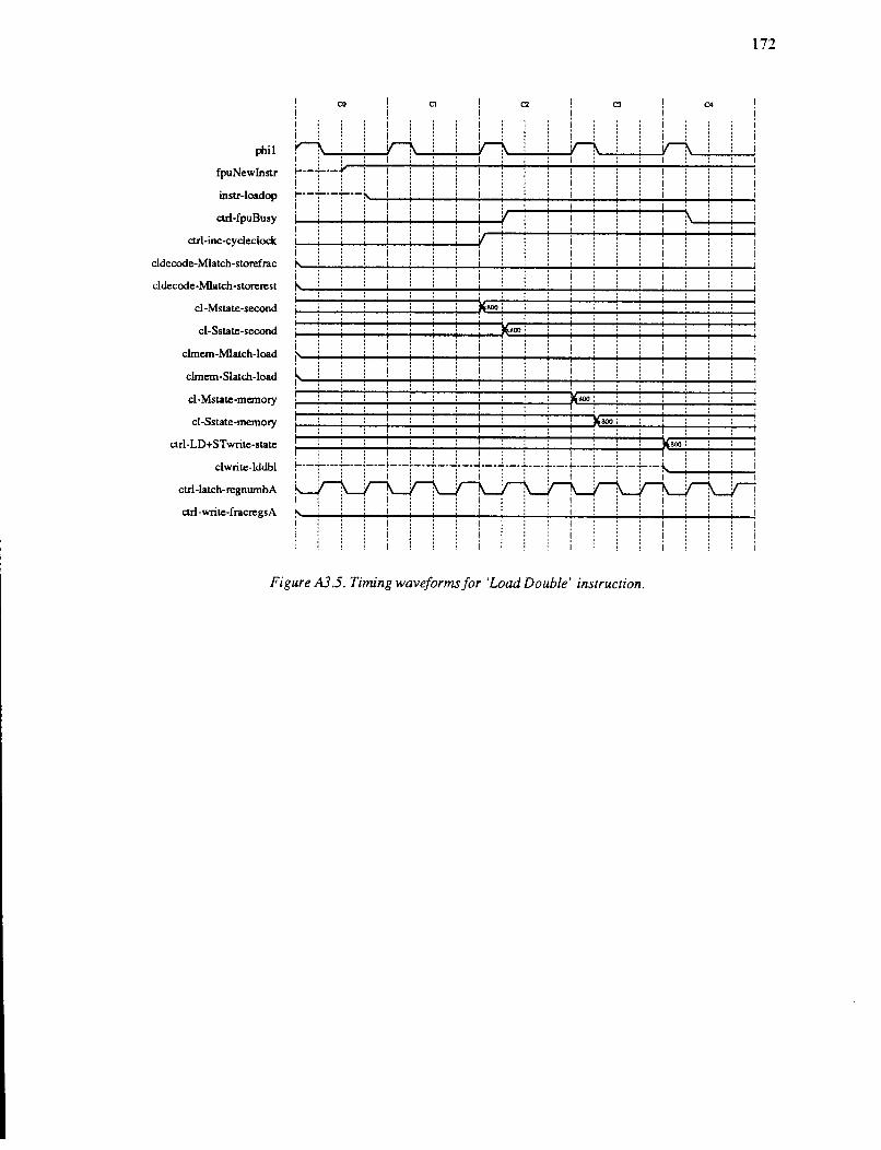
phil
fpuNewinstr
instr-loadop
ctrl-fpuBusy
ctrl-inc-cycleclock
cldecode-Mlatch-storefrac
cldecode-Mlatch-storerest
cl-Mstate-second
cl-Sstate-second
clmem-Mlatch-load
clmem-Slatch-load
cl-Mstate-memory
cl-Sstate-memory
ctrl-LD+STwrite-state
clwrite-lddbl
ctrl-latch-regnumbA
ctrl-write-fracregsA
172
co C1 C2 C4
~+-~~-+~--~+-~k~~~:--~~~~~--~~~~~~
~ ~~ioo~j~~~~~~-+~ i : :
~~_.--~~-+--~~~--+-_.~~~-+~--~~~--+-~~~~~ ri ~~+-+-~~~-+~~~~~~~:~~~~~~ i i ~=~:....:-; ~__,_-:---:---:---t : 14soo
: : : : : : : : : I : : : I =;;~--i---:-----t
~--t·-1---j---~-·-t-·-+-·i·-·t-·i·-·t·-·t·--t·-·i·--~·-t·-~ ..... --t----+---i
Figure A3.5. Timing waveforms for 'Load Double' instruction.
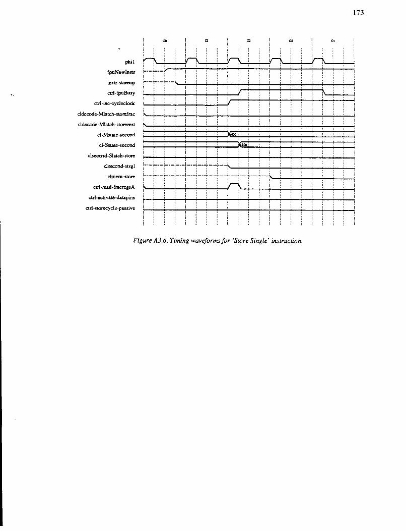
'·
phil
fpuNewinstr
instr-ston:op
ctrl-fpuBusy
ctrl-inc-cycleclodc
cldecode-Mlatch-storclrac
cldecode-Mlatch -st.orerest
cl-Mstate-second
cl-Sstate-second
clsecond-Slatch-store
clsecond-stsgl
clmem-store
ctrl-read-fracregs A
ctrl-activate-datapins
ctrl-storecycle-passive
173
a C2 C3 c•
I
! r. --:-. --:-. --:'--+--~--~~--_.:--~--~~--~--~--~~--~----~--~~ ~~ -.i~i--+-~~~--~+i~V ~~~_.~ ! : lr-~1--~------~~--~--._--~-+--~----~ ~! --i--~----~~--~~--~~ ! !
~~~~--~--~~~~~--:--~~--~~--~~~~~~
: ~~~~~-----~~-+-+-~~ ! : :
t:=t:=t:=!=:=t=:i=:j=:j:=:±-----~.;..: -----~-----~t-._-_+(_.___,___;,_+-....... ___, _ _,__, I : : ' I ! : : I ! ' : I -~--.;_--.;_-;.--~--.;__; __ -i l:: i::: n·. : i I ' ' I ' ' ' ' !'-· ~~·~~~-+-~ ...... -~~-~~~ i i i i i
Figure A3.6. Timing waveforms for 'Store Single' instruction.