by shahab poshtkouhi - university of toronto t-space · abstract modular ac nano-grid with...
TRANSCRIPT

Modular AC Nano-Grid with Four-QuadrantMicro-Inverters and High-Efficiency DC-DC Conversion
by
Shahab Poshtkouhi
A thesis submitted in conformity with the requirementsfor the degree of Doctor of Philosophy
Graduate Department of Electrical and Computer EngineeringUniversity of Toronto
Copyright © 2016 by Shahab Poshtkouhi

Abstract
Modular AC Nano-Grid with Four-Quadrant Micro-Inverters and High-Efficiency
DC-DC Conversion
Shahab Poshtkouhi
Doctor of Philosophy
Graduate Department of Electrical and Computer Engineering
University of Toronto
2016
A significant portion of the population in developing countries live in remote communi-
ties, where the power infrastructure and the required capital investment to set up local
grids do not exist. This is due to the fuel shipment and utilization costs required for
fossil fuel based generators, which are traditionally used in these local grids, as well as
high upfront costs associated with the centralized Energy Storage Systems (ESS). This
dissertation targets modular AC nano-grids for these remote communities developed at
minimal capital cost, where the generators are replaced with multiple inverters, con-
nected to either Photovoltaic (PV) or battery modules, which can be gradually added
to the nano-grid. A distributed droop-based control architecture is presented for the PV
and battery Micro-Inverters (MIV) in order to achieve frequency and voltage stability, as
well as active and reactive power sharing. The nano-grid voltage is regulated collectively
in either one of four operational regions. Effective load sharing and transient handling
are demonstrated experimentally by forming a nano-grid which consists of two custom
500 W MIVs.
The MIVs forming the nano-grid have to meet certain requirements. A two-stage MIV
architecture and control scheme with four-quadrant power-flow between the nano-grid,
the PV/battery and optional short-term storage is presented. The short-term storage
is realized using high energy-density Lithium-Ion Capacitor (LIC) technology. A real-
ii

time power smoothing algorithm utilizing LIC modules is developed and tested, while
the performance of the 100 W MIV is experimentally verified under closed-loop dynamic
conditions.
Two main limitations of the DAB topology, as the core of the MIV architecture’s dc-dc
stage, are addressed: 1) This topology demonstrates poor efficiency and limited regulation
accuracy at low power. These are improved by introducing a modified topology to operate
the DAB in Flyback mode, achieving up to an 8% increase in converter efficiency. 2) The
DAB topology needs four digital isolators for driving the active switches on the other
side of the isolation boundary. Two Phase-Locked-Loop (PLL) based synchronization
schemes are introduced in order to reduce the number of required digital isolators, hence
increasing reliability and reducing the implementation costs. One of these schemes is
demonstrated on a discrete 150 W DAB prototype, while both of them are implemented
on-chip in a 0.18µm 80V BCD process. In addition, the power-stage of the primary-side
of a 1 MHz, 50 W DAB converter is fully integrated on the same die. By using such a
high switching frequency, the size of passive elements in the DAB is reduced, resulting
in further cost reductions for the MIV.
The results of this dissertation pave the way for affordable nano-grids with minimal
capital cost, reliable performance and reduced complexity.
iii

Acknowledgements
“You are not a drop in the ocean, you are the entire ocean in a drop.”
– Rumi, 13th century Persian poet, jurist and scholar
First and foremost, I would like to thank my doctoral advisor, Professor Olivier
Trescases, for his exceptional level of guidance and support throughout my entire graduate
studies. Every time I left his office after a research meeting, I was more motivated
and much happier than when I was going in. His wisdom and vast technical knowledge
catalyzes unique synergies within “OTgrp”, our research group which I have been a proud
member of since its early days of foundation. I have learned so much from Olivier, not
only in the technical aspect, but also in business, management, and personal networking,
for which I will always be grateful.
I have had the pleasure of collaborating with many forward-looking companies as
well as a great number of talented individuals. I want to thank Solantro Semiconductor
for their visionary outlook and keen interest in niche humanitarian applications, which
prompted the nano-grid project. In particular, I have had the honor of working closely
with Ray Orr and Ben Bacque, whose creative approach to solving technical difficulties
has had a lasting influence on me. I also want to thank Mihai Varlan, Tony Reinberger,
Chris Gerolami, Nikolay Radimov, Edward Keyes, Edward MacRobbie, and Christian
Cojocaru from Solantro Semiconductor for their technical support and long fruitful dis-
cussions during my internship at Solantro. I have learned a lot from all of them. I have
had the pleasure of collaborating with Magnachip Semiconductor for the IC design and
fabrication presented in Chapter 5. I want to thank Michael Sun and Ikjoon Choi for
securing the silicon space on one of their highly popular shuttle runs as well as providing
much needed technical support throughout the design stage. I would like to express my
sincere gratitude to David King Li for his continuous effort on IDP (Chapter 2), Hus-
sam Hussein and Aliakbar Eski, for their significant contributions to the development
iv

and testing of many DAB prototypes (Chapters 3 and 4), and Miad Fard, for his valued
cooperation in the design and testing of the SPM IC (Chapter 5). This thesis would not
have got so far without their important contributions.
I want to thank all the friends I have made and worked with in my graduate studies.
I will never forget my shared memories with Victor (Yue) Wen, Mazhar and Andishe
Moshirvaziri, Vishal Palaniappan, Shuze Zhao, Shawkat Zaman, Steven Chung, Masa-
fumi Otsuka, and Ahmad Diab Marzouk. I thank them for the discussion, encouragement,
and friendship.
I received generous financial support from Ontario Centres of Excellence (OCE),
Solantro Semiconductor, Hatch, NSERC, OGS, and Rogers Graduate Scholarship. With-
out this funding, my Ph.D. would not have been as smooth as it was. I acknowledge the
support from all these sources.
I know that I can never be thankful enough to my mother, whose hard work and
ambitions have always been the main source of inspiration to me. I know that I can
never fully embrace all the dedications and sacrifices my father has done for me. If I were
to choose, I could not have possibly asked for better parents, whose unconditional love
and support have always been there for me.
I definitely cannot thank Tania enough. Now that I look back at it, I know that
I found her just in time, at a time when I was overwhelmed with stress and endless
uncertainties. Her patience and understanding boosted me through this rough stage of
my life. Had it not been for her, my Ph.D. track would have been longer, harder, and
definitely lonelier. I admit that when I developed the “smoothing” algorithm in Chapter
3, I did not believe it could be done any better any smoother. Well, she never stops
proving me wrong, and I love it.
v

Contents
1 Introduction 1
1.1 Modular AC Nano-Grids . . . . . . . . . . . . . . . . . . . . . . . . . . . 4
1.2 Bidirectional Topologies . . . . . . . . . . . . . . . . . . . . . . . . . . . 8
1.3 Thesis Outline and Objectives . . . . . . . . . . . . . . . . . . . . . . . . 9
2 Nano-Grid Architecture and Control 18
2.1 Proposed Droop Control . . . . . . . . . . . . . . . . . . . . . . . . . . . 19
2.1.1 Nano-Grid Voltage Partitioning . . . . . . . . . . . . . . . . . . . 24
2.1.2 PV and Battery Inverter Control . . . . . . . . . . . . . . . . . . 24
2.2 Nano-Grid Test Case . . . . . . . . . . . . . . . . . . . . . . . . . . . . . 30
2.3 Nano-Grid Experimental Results . . . . . . . . . . . . . . . . . . . . . . 35
2.4 Chapter Summary . . . . . . . . . . . . . . . . . . . . . . . . . . . . . . 39
3 MIV Architecture and Control 43
3.1 DC-DC Stage . . . . . . . . . . . . . . . . . . . . . . . . . . . . . . . . . 44
3.2 DC-AC Stage . . . . . . . . . . . . . . . . . . . . . . . . . . . . . . . . . 48
3.3 Short-Term Storage . . . . . . . . . . . . . . . . . . . . . . . . . . . . . . 49
3.4 Power Smoothing Algorithm . . . . . . . . . . . . . . . . . . . . . . . . . 50
3.5 Experimental Results . . . . . . . . . . . . . . . . . . . . . . . . . . . . . 54
3.5.1 MIV Operation . . . . . . . . . . . . . . . . . . . . . . . . . . . . 54
3.5.2 Smoothing Algorithm Performance Evaluation . . . . . . . . . . . 57
vi

3.6 Chapter Summary . . . . . . . . . . . . . . . . . . . . . . . . . . . . . . 60
4 DAB Converter: Drawbacks and Enhancements 64
4.1 Low-Power Efficiency Enhancement . . . . . . . . . . . . . . . . . . . . . 65
4.1.1 Modified DAB Architecture and Principle of Operation . . . . . . 65
DAB Mode . . . . . . . . . . . . . . . . . . . . . . . . . . . . . . 66
Flyback Mode . . . . . . . . . . . . . . . . . . . . . . . . . . . . . 66
Dual Mode Control . . . . . . . . . . . . . . . . . . . . . . . . . . 70
4.1.2 Regulation Accuracy at Low Power . . . . . . . . . . . . . . . . . 70
4.1.3 Transformer Design . . . . . . . . . . . . . . . . . . . . . . . . . . 73
4.1.4 Efficiency Analysis . . . . . . . . . . . . . . . . . . . . . . . . . . 75
Conduction Losses . . . . . . . . . . . . . . . . . . . . . . . . . . 75
Switching Losses . . . . . . . . . . . . . . . . . . . . . . . . . . . 77
Core Losses . . . . . . . . . . . . . . . . . . . . . . . . . . . . . . 77
Loss Comparison in Two Modes . . . . . . . . . . . . . . . . . . . 78
4.1.5 Simulation and Experimental Results . . . . . . . . . . . . . . . . 79
4.2 Reliability and Isolation . . . . . . . . . . . . . . . . . . . . . . . . . . . 83
4.2.1 PTS Scheme for the DAB Topology . . . . . . . . . . . . . . . . . 87
Digital PLL Implementation Scheme and Analog Interface . . . . 90
Data Transmission . . . . . . . . . . . . . . . . . . . . . . . . . . 92
4.2.2 Effect of Transformer Leakage Inductance . . . . . . . . . . . . . 92
4.2.3 Extension to Other Isolated Bidirectional Topologies . . . . . . . 96
4.2.4 Experimental Results . . . . . . . . . . . . . . . . . . . . . . . . . 99
4.3 Chapter Summary . . . . . . . . . . . . . . . . . . . . . . . . . . . . . . 104
5 On-Chip Synchronization and Integrated DAB Converter 110
5.1 PLL Implementation . . . . . . . . . . . . . . . . . . . . . . . . . . . . . 111
5.2 DIS Scheme Synchronization . . . . . . . . . . . . . . . . . . . . . . . . . 113
vii

5.3 PTS Scheme Synchronization . . . . . . . . . . . . . . . . . . . . . . . . 116
5.4 Integrated Power Stage . . . . . . . . . . . . . . . . . . . . . . . . . . . . 117
5.5 Experimental Results . . . . . . . . . . . . . . . . . . . . . . . . . . . . . 121
5.6 Chapter Summary . . . . . . . . . . . . . . . . . . . . . . . . . . . . . . 130
6 Conclusions 134
6.1 Contributions . . . . . . . . . . . . . . . . . . . . . . . . . . . . . . . . . 135
6.2 Future Work . . . . . . . . . . . . . . . . . . . . . . . . . . . . . . . . . . 137
A Intelligent Distribution Panel 140
A.1 IDP Architecture . . . . . . . . . . . . . . . . . . . . . . . . . . . . . . . 140
A.2 Measurements and Processing . . . . . . . . . . . . . . . . . . . . . . . . 143
A.3 IDP Experimental Results . . . . . . . . . . . . . . . . . . . . . . . . . . 145
A.4 Appendix Summary . . . . . . . . . . . . . . . . . . . . . . . . . . . . . . 148
B Household Load Modeling and Emulation 150
B.1 Load Profile Acquisition . . . . . . . . . . . . . . . . . . . . . . . . . . . 150
B.2 Load Profile Emulation . . . . . . . . . . . . . . . . . . . . . . . . . . . . 151
B.3 Appendix Summary . . . . . . . . . . . . . . . . . . . . . . . . . . . . . . 155
viii

List of Tables
1.1 Comparison of AC and DC Micro and Nano-Grids . . . . . . . . . . . . . 6
2.1 Operational Regions of Vg and Interpretations for PV/Battery MIVs and
Local Loads . . . . . . . . . . . . . . . . . . . . . . . . . . . . . . . . . . 25
2.2 Parameters of the Simulated Nano-Grid . . . . . . . . . . . . . . . . . . . 31
3.1 MIV Prototype Specifications . . . . . . . . . . . . . . . . . . . . . . . . 54
3.2 LIC and PV Specifications . . . . . . . . . . . . . . . . . . . . . . . . . . 58
4.1 Dual Mode DAB Converter Prototype Specifications . . . . . . . . . . . . 81
4.2 DAB Converter with PTS Scheme Prototype Specifications . . . . . . . . 100
5.1 DAB Converter Prototype Specifications with External Power Stage . . . 123
5.2 DAB Converter Prototype Specifications with Internal Power Stage as
Primary-Side . . . . . . . . . . . . . . . . . . . . . . . . . . . . . . . . . 127
5.3 Comparison of Driving Schemes in Isolated Converters . . . . . . . . . . 131
A.1 Comparison of IDP MSOGI-FLL Outputs and Readings from E-Load for
Four Test Cases . . . . . . . . . . . . . . . . . . . . . . . . . . . . . . . . 147
ix

List of Figures
1.1 Projected world energy consumption between 2010 and 2040 [1]. . . . . . 2
1.2 Visualization of the remote places on earth, created by the European Com-
missions Joint Research Centre and the World Bank [6]. . . . . . . . . . 2
1.3 Price history of silicon PV cells ($/Wp) [8]. . . . . . . . . . . . . . . . . . 3
1.4 Architecture of (a) a nano-grid with central ESS and generator, and (b)
the proposed modular nano-grid. . . . . . . . . . . . . . . . . . . . . . . 7
1.5 Two-stage MIV architecture with integrated storage targeted in this work. 10
1.6 The full system implementation of the nano-grid. . . . . . . . . . . . . . 11
2.1 Equivalent Thevenin model of a single MIV connected to the nano-grid. . 20
2.2 P -V droop characteristic for (a) battery, and (b) PV MIVs. . . . . . . . 22
2.3 Q-f droop characteristic for battery and PV MIVs. . . . . . . . . . . . . 23
2.4 Control approaches for the PV and battery inverters based on regulation
of virtual resistance and the synthetic internal voltage. . . . . . . . . . . 25
2.5 (a) P , and (b) Q for the two parallel battery inverters with different SOC.
SOCn1 = 0.25, and SOCn2 = 0.1. The inverters are cold started at t = 0 s. 28
2.6 (a) P , and (b) Q for the two parallel battery inverters with different series
resistances. RL1 = 0.1 Ω, and RL2 = 0.3 Ω. . . . . . . . . . . . . . . . . . 29
2.7 Block diagram of the inverter control implementation. . . . . . . . . . . . 30
2.8 The RMS nano-grid voltage, Vg, throughout the simulated test scenario. . 31
2.9 The real power of MIV1-5, P1−5, throughout the simulated test scenario. 32
x

2.10 The reactive power of MIV1-5, Q1−5, throughout the simulated test scenario. 32
2.11 Simulated (a) vg(t), and (b) ig1−5(t) for t = [9.8-10.2] s. At t = 10 s, the
reactive load of 600 VAR is removed, and a real load-step of 1000 W is
introduced. . . . . . . . . . . . . . . . . . . . . . . . . . . . . . . . . . . 34
2.12 Experimental testbench for two parallel battery/PV inverters with RLC
load bank. . . . . . . . . . . . . . . . . . . . . . . . . . . . . . . . . . . . 35
2.13 Start-up of MIV1, while MIV2 is not active (P = 200 W and Q = 0 VAR). 35
2.14 MIV1 operation, while MIV2 is not active. MIV2 draws reactive power
due to its output filter. . . . . . . . . . . . . . . . . . . . . . . . . . . . . 36
2.15 (a) The reference and measured nano-grid frequency. (b) The active and
reactive components of grid current, Igd and Igq. The load transient is 200
W - 160 VAR → 200 W + 0 VAR. . . . . . . . . . . . . . . . . . . . . . 36
2.16 Parallel operation and transient response of the two battery inverter sys-
tem, with SOCn1 = SOCn2 = 0.5. The load transient is 400 W - 42 VAR
→ 200 W + 0 VAR. . . . . . . . . . . . . . . . . . . . . . . . . . . . . . 37
2.17 Parallel operation and transient response of two battery inverter, with
SOCn1 = 2SOCn2 = 0.5. The load transient is 280 W + 0 VAR → 280
W + 153 VAR. . . . . . . . . . . . . . . . . . . . . . . . . . . . . . . . . 37
2.18 Parallel operation of one PV inverter (MIV1), and one battery inverter
(MIV2). The PV inverter is delivering its MPP power of 420 W, and the
remaining 80 W is supplied by the battery inverter. . . . . . . . . . . . . 38
3.1 Two-stage MIV architecture with integrated storage. . . . . . . . . . . . 43
3.2 (a) Architecture, and (b) simplified control diagram for the dc-dc stage. . 46
3.3 Switching waveforms of the DAB. . . . . . . . . . . . . . . . . . . . . . . 47
3.4 (a) Architecture and (b) simplified control diagram for the dc-ac stage. . 49
3.5 (a) Physical structure of Lithium-Ion Capacitor [13]. (b) Ragone plot for
different storage technologies [14]. . . . . . . . . . . . . . . . . . . . . . . 51
xi

3.6 Power smoothing and LIC SOC control. . . . . . . . . . . . . . . . . . . 53
3.7 Measured efficiency of the DAB, LIC and dc-ac stages. . . . . . . . . . . 55
3.8 Steady-state waveforms for the DAB converter (ILDAB:5 A/div). . . . . . 55
3.9 Step changes in (a) Vpv,ref , and (b) ILIC,ref (ILIC :2 A/div). . . . . . . . . 56
3.10 MIV dynamic response at unity power factor with two consecutive P steps,
40 W → 16 W → 40 W (Ig:0.2 A/div). . . . . . . . . . . . . . . . . . . . 57
3.11 (a) PV power, Ppv, the running average, Ppv,ave, the fitted polynomial,
s(θ), and the LIC power, PLIC . (b) dPdt, ds(θ)
dt, and (c) VLIC for a typical
cloudy day. . . . . . . . . . . . . . . . . . . . . . . . . . . . . . . . . . . 59
4.1 a) Proposed modified DAB dc-dc topology for improved low power effi-
ciency. b) Switch configuration in Flyback mode. . . . . . . . . . . . . . 67
4.2 Switching waveforms in (a) DAB mode with optimized DC-link voltage
(Vbus = nVin), and (b) Flyback mode. . . . . . . . . . . . . . . . . . . . . 68
4.3 Simplified conceptual control diagram of the modified DAB converter. . . 71
4.4 (a) PDAB and dPDAB
dtdin DAB mode, and (b) PDAB and dPDAB
dTsin Flyback
mode. . . . . . . . . . . . . . . . . . . . . . . . . . . . . . . . . . . . . . 72
4.5 (a) Planar transformer used in this work for dual-mode operation, and (b)
typical B-H curve for C95 magnetic material [11]. . . . . . . . . . . . . . 74
4.6 Simulated power losses for (a) P = 10 W, and (b) P = 40 W. . . . . . . 78
4.7 Steady-state waveforms of the converter in (a) DAB mode without dy-
namically adjusted DC link voltage, (b) DAB mode with adjusted DC
link voltage (Vbus = n Vin) at Vin = 22 V (ILDAB:5 A/div), and (c) Fly-
back mode at Vin = 25 V (ILDAB:5 A/div). . . . . . . . . . . . . . . . . . 80
4.8 Simulated ILDAB and ILm in Flyback mode operating in CCM. . . . . . . 82
4.9 Measured step-response of Flyback mode: PDAB: 9.1 W → 19.5 W (Iin:0.2
A/div, ILDAB: 10 A/div). . . . . . . . . . . . . . . . . . . . . . . . . . . 82
4.10 Measured efficiency, η, of the converter. . . . . . . . . . . . . . . . . . . . 83
xii

4.11 Architecture of a two-stage bidirectional MIV with (a) one digital isolator
per transistor and additional isolators for communication between stages,
(b) DIS scheme requiring isolators only for communication, and (c) pro-
posed PTS scheme where the switching information are extracted from the
power transformer on the primary-side. . . . . . . . . . . . . . . . . . . . 85
4.12 (a) High-frequency digital isolator with capacitive or magnetic isolation.
(b) Typical operating waveforms. . . . . . . . . . . . . . . . . . . . . . . 86
4.13 DAB dc-dc converter with (a) primary-side and (b) secondary-side con-
troller utilizing conventional digital isolators. . . . . . . . . . . . . . . . . 88
4.14 DIS synchronization scheme for the DAB topology. . . . . . . . . . . . . 89
4.15 PTS synchronization scheme for the DAB topology. . . . . . . . . . . . . 89
4.16 PLL implementation for clock synchronization across the DAB transformer.
The primary-side bridge is not shown. The phase selection for the DAB
converter (seltp) can be performed either by a voltage, power or MPPT
control loop (as shown here). . . . . . . . . . . . . . . . . . . . . . . . . . 90
4.17 (a) Startup of the synchronization process. (b) Proposed communication
scheme based on frequency modulation. . . . . . . . . . . . . . . . . . . . 91
4.18 Single-comparator sensing for the PTS scheme with the leakage inductance. 93
4.19 (a) Waveforms for Vsns and comp when (4.26) is satisfied and (b) when
(4.26) is not satisfied, causing the PLL to lock to the primary-side which
leads to system instability. . . . . . . . . . . . . . . . . . . . . . . . . . . 94
4.20 (a) Simulated FPGA core voltage, Vcore, and (b) zoomed out, and (c)
zoomed in DAB inductor current, ILDAB, with single-comparator solution.
The large leakage inductance introduced at t = 3.5 ms causes the PLL to
become unstable. . . . . . . . . . . . . . . . . . . . . . . . . . . . . . . . 95
4.21 (a) Simulated Vsns, and (b) comp signal with single-comparator solution
(time-scale:10 µs/div). . . . . . . . . . . . . . . . . . . . . . . . . . . . . 96
xiii

4.22 The proposed two-comparator solution to generate the comp signal. c3
denotes the gating signal to the switch M3. . . . . . . . . . . . . . . . . . 97
4.23 (a) Simulated FPGA core voltage, Vcore, and (b) zoomed in DAB inductor
current, ILDAB, with two-comparator solution (time-scale:10 µs/div). The
PLL is stable despite the introduction of a large leakage inductance at t
= 3.5 ms. . . . . . . . . . . . . . . . . . . . . . . . . . . . . . . . . . . . 97
4.24 (a) Simulated Vsns, and (b) comp signal with two-comparator solution
(time-scale:10 µs/div). . . . . . . . . . . . . . . . . . . . . . . . . . . . . 98
4.25 Additional candidate topologies for the PTS scheme; (a) Bidirectional
flyback [33], and (b) full-bridge push-pull based topology [34]. . . . . . . 99
4.26 The 150 W DAB converter prototype which includes no digital isolators.
The controller is implemented on an FPGA board (not shown). . . . . . 100
4.27 Measured DAB waveforms in steady-state (ILDAB:1/3 A/div, Vx2:500 V/div
(attenuated by 10×). . . . . . . . . . . . . . . . . . . . . . . . . . . . . . 101
4.28 Measured efficiency of the DAB converter at two different switching fre-
quencies. . . . . . . . . . . . . . . . . . . . . . . . . . . . . . . . . . . . . 101
4.29 Measured unit time delay versus core voltage for the VCO in the primary-
side controller. . . . . . . . . . . . . . . . . . . . . . . . . . . . . . . . . . 102
4.30 Measured PLL locking in the DAB converter, showing synchronization of
the two bridges without any digital isolators resulting in the activation of
the DAB converter. . . . . . . . . . . . . . . . . . . . . . . . . . . . . . . 102
4.31 Frequency-modulation based data communication. Vgs3 denotes the gate-
to-source voltage of MOSFET M3, controlled by gate signal c3. . . . . . . 103
5.1 Simplified architecture of the two proposed synchronization schemes (DIS
and PTS) implemented on a DAB dc-dc converter. . . . . . . . . . . . . 111
5.2 The IC block diagram of the PTS and DIS schemes, and the precise phase-
shift generation. . . . . . . . . . . . . . . . . . . . . . . . . . . . . . . . . 112
xiv

5.3 The simulated delay-line frequency, fdl, vs. the bias voltage, Vc. . . . . . 113
5.4 Schematics of (a) the loop-filter, and (b) the phase-detector block. . . . . 114
5.5 Two-chip GISO transmission simulation at 100 MHz bitstream. . . . . . 115
5.6 GISO packet including the preamble and data periods. The PLL is acti-
vated during preamble period. . . . . . . . . . . . . . . . . . . . . . . . . 116
5.7 (a) The on-chip half-bridge with over-current protection, and (b) the full
primary-side power-stage of the DAB converter. . . . . . . . . . . . . . . 118
5.8 The schematic of the gate-driver circuit. . . . . . . . . . . . . . . . . . . 119
5.9 (a) Schematic, and (b) simulated operating waveforms of the high-side
level-shifter at Vin = 70 V. . . . . . . . . . . . . . . . . . . . . . . . . . . 120
5.10 The programmable dead-time block. . . . . . . . . . . . . . . . . . . . . 120
5.11 Schematic of the over-temperature protection block. . . . . . . . . . . . . 121
5.12 (a) The layout, and (b) the packaged chip micrograph (2.5×4.5 mm2 in
0.18µm 80V BCD process). . . . . . . . . . . . . . . . . . . . . . . . . . 122
5.13 (a) Start-up, and (b) steady state operation of the synchronization process
in the DIS mode. . . . . . . . . . . . . . . . . . . . . . . . . . . . . . . . 124
5.14 (a) Start-up, and (b) steady state operation of the synchronization process
in the PTS mode. . . . . . . . . . . . . . . . . . . . . . . . . . . . . . . . 125
5.15 Synchronized DAB converter waveforms in the (a) DIS mode with contin-
uous GISOin input clock, and (b) PTS mode (ILDAB: 5A/div). . . . . . 126
5.16 The power stage of the 1 MHz DAB converter with internal primary-side
bridge. The IC is soldered on a separate board and is placed face down
on the main power board. . . . . . . . . . . . . . . . . . . . . . . . . . . 127
5.17 Switching waveforms of the integrated DAB converter at Vin = 40 V, Vbus
= 115 V, and PDAB = 45 W (ILDAB = 1 A/div). . . . . . . . . . . . . . 128
5.18 The efficiency of the DAB converter with integrated primary-side for dif-
ferent Vin and Vbus. . . . . . . . . . . . . . . . . . . . . . . . . . . . . . . 128
xv

5.19 The zoomed-in primary-side switching nodes V1 and V2 (Vin = 35 V). . . 129
5.20 Primary-side shut-down due to (a) over-current, and (b) over-temperature
faults (ILDAB = 1 A/div). . . . . . . . . . . . . . . . . . . . . . . . . . . 129
A.1 IDP Architecture. . . . . . . . . . . . . . . . . . . . . . . . . . . . . . . . 141
A.2 Assembled Power and DAQ boards. . . . . . . . . . . . . . . . . . . . . . 142
A.3 The IDP motherboard PCB (top view). . . . . . . . . . . . . . . . . . . . 143
A.4 SOGI-FLL architecture [3]. . . . . . . . . . . . . . . . . . . . . . . . . . . 144
A.5 Simulation results for MSOGI-FLL demonstrating the start-up and suc-
cessful locking to the (a) frequency, and (b) fundamental and harmonics
contents of u(t). . . . . . . . . . . . . . . . . . . . . . . . . . . . . . . . . 145
A.6 Assembled ten-channel IDP. . . . . . . . . . . . . . . . . . . . . . . . . . 146
A.7 The smart breaker command and AC line current when (a) connecting,
and (b) disconnecting the channel. . . . . . . . . . . . . . . . . . . . . . 146
B.1 (a) The load acquisition setup diagram, and (b) the modified double-socket
power outlet receptacle. . . . . . . . . . . . . . . . . . . . . . . . . . . . 151
B.2 Grid voltage and steady-state AC current of a typical (a) small fan, and
(b) microwave (Vg attenuated by 100×). . . . . . . . . . . . . . . . . . . 152
B.3 The load characterization process. . . . . . . . . . . . . . . . . . . . . . . 153
B.4 (a) The AC current measurement, and (b) the reconstructed waveform for
a typical 60 W laptop charger in idle state (not charging). . . . . . . . . 154
xvi

List of Acronyms
EIA: Energy Information Association
OECD: Organization for Economic Cooperation and Development
Btu: British thermal units
PV: Photovoltaic
ESS: Energy Storage System
BMS: Battery Management System
MIV: Micro-Inverter
MPPT: Maximum Power Point Tracking
THD: Total Harmonic Distortion
IDP: Intelligent Distribution Panel
SOC: State-of-Charge
DAB: Dual-Active-Bridge
DC: Direct Current
AC: Alternating Current
IC: Integrated Circuit
DER: Distributed Energy Resources
PCC: Point of Common Coupling
EMI: Electromagnetic Interference
VSI: Voltage Source Inverter
CSI: Current Source Inverter
LIC: Lithium-Ion Capacitor
LUT: Look-Up Table
EDLC: Electric Double Layer Capacitor
ESR: Equivalent Series Resistance
xvii

BIPV: Building-Integrated Photovoltaic
BCM: Boundary Conduction Mode
PC: Personal Computer
FPGA: Field Programmable Gate Array
BVS: Bus Voltage Scaling
ZVS: Zero-Voltage-Switching
LSB: Least Significant Bit
CCM: Continuous Conduction Mode
SiP: System-in-Package
PWM: Pulse-Width-Modulation
Mbps: Mega bit-per-second
DIS: Digital Isolator Sensing
PTS: Power Transformer Sensing
PLL: Phase-Locked-Loop
PSM: Phase-Shift-Modulation
VCO: Voltage Controlled Oscillator
DAC: Digital-to-Analog Converter
CMOS: Complementary MetalOxideSemiconductor
CPLD: Complex Programming Logic Device
TTL: Transistor-Transistor Logic
BCD: Bipolar CMOS DMOS
SPI: Serial Peripheral Interface
GUI: Graphical User Interface
GISO: Galvanically Isolated interface
PCB: Printed Circuit Board
UPS: Uninterruptible Power Supply
DAQ: Data Acquisition
xviii

ADC: Analog-to-Digital Converter
CPU: Central Processing Unit
BBB: BeagleBone Black
FFT: Fast Fourier Transform
SOGI: Second Order General Integrator
MSOGI-FLL: Multiple Second Order General Integrator - Frequency-Locked-Loop
PF: Power Factor
CF: Crest Factor
xix

Chapter 1
Introduction
As projected by the U.S. Energy Information Administration (EIA), the total world
energy demand is expected to grow by 56% between 2010 and 2040, as shown in Fig. 1.1
[1]. The world’s total energy consumption growth rate is predicted to be between 1.3%
and 1.4% on average between 2020 and 2035 [1]. Most of this growth will come from
non-OECD (non-Organization for Economic Cooperation and Development) countries,
where demand is driven by strong economic growth and rising population [1]. China
and India mark two of the biggest countries in this category with the highest growth in
projected energy demand. In fact, while the energy use per capita for OECD countries
is anticipated to remain almost the same by 2040, it is predicted to rise by 46% for
non-OECD countries, from 50 Million British thermal units (MBtu) to 73 MBtu per
capita [1].
This upward trend in energy consumption is mostly due to the increasing use of
electricity by the industrial sector, despite technological improvements in operational
efficiency [2, 3]. However, the energy demand for rural areas and remote isolated com-
munities in developing countries has been increasing, as they host about half of the total
population in these countries [4]. By definition, a remote community is a community that
is either located far from highly populated settlements, or lacks transportation links that
1

Chapter 1. Introduction 2
Figure 1.1: Projected world energy consumption between 2010 and 2040 [1].
are typical in more populated areas [5]. The planet’s most logistically remote locations
are highlighted in Fig. 1.2 by considering their ground travel time to the nearest city
having a population of at least 50,000 people [6]. As of 2009, 292 remote communities
existed in Canada, with a total population of approximately 200,000 people [7].
Figure 1.2: Visualization of the remote places on earth, created by the European Commissions
Joint Research Centre and the World Bank [6].
Most of the remote communities in Canada are off-grid and powered by fossil fuel
generators, namely diesel and gasoline [7]. However, the high cost of maintenance and
fuel transport together with the decreasing cost of solar installations make the integration

Chapter 1. Introduction 3
Figure 1.3: Price history of silicon PV cells ($/Wp) [8].
of solar energy very attractive [9]. For instance, the residential monthly electricity charge
in the Northwest Territories has a median of C$0.72/kWh [10], while the average cost of
electricity from PV generation was reduced to between US$0.11 and US$0.13 for North
American installations in 2014 [11]. This difference compensates for the lack of solar
irradiation in these territories. The average price-per-peak power ($/Wp) of commercial
silicon photovoltaic (PV) cells reached US$0.30 in 2015, and continues to shrink, as shown
in Fig. 1.3 [12]. The inverter costs have also been shrinking between 10-15% annually [13].
Efforts have been made to realize renewable energy integration in remote communities.
The solar installation is generally implemented as a supplement to the existing fossil fuel
plants. A 70 kW off-grid PV system installation and integration with diesel generators
for a remote community in Canada is discussed in [10].
In applications involving remote communities and villages, there is a need for modular

Chapter 1. Introduction 4
power electronics with minimal capital cost, while allowing gradual expansion of gener-
ation capacity. Due to high initial costs of conventional solar installations, it is essential
to follow a modular model for sustainable growth of generation and storage capacity
in remote communities with very limited budgets for infrastructure. The intermittent
nature of PV, and thus the need for storage, is a major challenge, even if power-quality
and grid requirements are reduced compared to large-scale grids due to the types of loads
and isolated nature of these applications.
AC nano-grids are independent systems with the following characteristics [14]:
1. They are off-grid systems.
2. They are below 20 kW in peak load power.
3. They consist of energy generation, storage and delivery.
4. They serve a single household, building, or loads in close proximity.
5. Several nano-grids can be connected together in order to share their loads and
resources.
In many ways, nano-grids can be considered as small micro-grids with lower power-
level [14]. There is a growing application base for AC nano-grids ranging from underpop-
ulated remote communities and research stations, to developing nations that lack reliable
power infrastructure [15].
This thesis targets AC nano-grids for remote communities, where PV modules are
used either as the sole energy source, or to supplement the existing fuel based generators.
Batteries are used as storage elements in the nano-grid.
1.1 Modular AC Nano-Grids
The energy consumption per capita of remote communities is significantly lower compared
to the urban areas. For instance, the minimum amount of target accessible energy per

Chapter 1. Introduction 5
rural and urban households in Africa is 250 kWh and 500 kWh per year, respectively
[16]. The average residential electricity consumption per capita for sub-Saharan Africa
including South Africa is 317 kWh per year. With South Africa excluded, this number
drops to 225 kWh per year (616 Wh per day) [16]. A single PV panel and battery
can provide this level of energy requirement, motivating a modular approach towards
establishing the nano-grid.
DC nano-grids have been proposed and deployed for lighting and powering substa-
tions. While they provide enormous benefits in terms of simplicity, they are limited in
scalability and range of applications. Furthermore, pricing and safety are two key concern
in DC grids due to expensive DC breakers and contactors with short lifetimes, primarily
because of the lack of zero crossing points in DC waveforms [17]. Despite slightly lower
conversion efficiency, AC nano-grids can be considered superior to DC nano-grids due to
the following:
1. The plethora of devices that are designed for AC operation.
2. Simple conversion between voltage levels by using transformers.
3. Low cost of protection devices.
A general comparison between AC and DC micro and nano-grids is provided in Table 1.1.
A typical AC nano-grid with Micro-Inverters (MIV) is shown in Fig. 1.4(a). The
Energy Storage System (ESS) is usually based on a large centralized bidirectional ac-dc
converter, connected to a battery bank [19, 20]. The ESS generally includes a Battery
Management System (BMS) with cell-level monitoring and balancing circuits. A fuel
based generator is also used, not only to provide energy, but to regulate the voltage
and frequency of the nano-grid. An alternative architecture consisting of distributed
storage rather than the centralized ESS is proposed in Fig. 1.4(b), which has the following
advantages:

Chapter 1. Introduction 6
Table 1.1: Comparison of AC and DC Micro and Nano-Grids
AC DC
Standards and Codes Well developed a Not fully developed
Installation and Easier, well understood More complex
Maintenance by electricians
Safety Issues Moderate High
Single-Phase Power Required Not applicable
Decoupling
Number of High, more Relatively low, fewer conversion stages
Electrical Components conversion stages to/from DC sources (PV, fuel cells, batteries)
Generation-to-Load Lower than DC Higher
Conversion Efficiency
ae.g. IEEE 1547 Series Standards [18]
1. There is no need for a large costly central inverter to be installed within the space-
limited confines of the household.
2. A generator is not needed, and the voltage and frequency are collectively regulated
by the MIVs. It should be noted that in case of remote areas where the amount of
available solar energy is low, there might be a need for a seasonal generator back-
up system. Alternatively, other renewable energy resources, such as wind, could be
justifiable in such places.
3. The architecture is highly modular and the generation capacity can be easily ex-
panded with limited cost due to the parallel architecture.
4. The labor component of the installation cost is reduced significantly for the battery
system, as there is no need to interface the large centralized DC storage unit to the
AC system.
For the sake of scalability and low capital costs, the nano-grid is configured as a collec-
tion of individual and autonomous PV and battery inverters connected to loads via an In-
telligent Distribution Panel (IDP), which provides monitoring, individual load/generation/storage

Chapter 1. Introduction 7
Vpvm
+
-
Ig
MIV
AC
Loads
Ipvm AC Module m
Central
ESS
Vpv1
+
-
MIV
Ipv1
Vg
+
-
AC Module 1
+
-
VpVV vm
+
-
MIVIpII vm AC Module m
VpVV v1
+
-
MIV
IpII v1 AC Module 1
AC Generator
(diesel)
(a)
AC load
Intelligent Distribution PanelUser
Interface
Battery
MIVs
PV
MIVs
Power Bus
AC load
AC load
Neighboring
nano-grid
(b)
Figure 1.4: Architecture of (a) a nano-grid with central ESS and generator, and (b) the proposed
modular nano-grid.

Chapter 1. Introduction 8
channel control, and a platform for high-level control. These elements function coopera-
tively to form an autonomous AC electrical grid of up to 20 kW in peak power delivery.
The system is designed such that multiple separate nano-grids can connect together
through the IDP forming a larger electrical grid.
1.2 Bidirectional Topologies
MIVs provide high-granularity distributed Maximum Power Point Tracking (MPPT)
at the module or sub-string level for PV units [21–23]. The MIV-based architecture
leads to increased robustness to clouds, dirt, and aging effects as well as irradiance
mismatches and temperature variations between different modules or sub-strings. Several
companies and PVmanufacturers have emerged in recent years aiming at developing these
architectures [24–26].
Existing MIVs satisfy the need for low capital-cost and expandable AC generation,
but not storage. There is compelling argument to extend this technology to include dis-
tributed storage. Integrated storage helps to buffer the frequent irradiance fluctuations,
as well as providing back-up power support if needed [27, 28]. With high penetration
of Distributed Energy Resources (DER) in developed electrical grids, the importance of
reactive power support from the interfacing inverters becomes more significant [29]. Poor
reactive support can result in instability in the local grid. Similarly, in small nano-grids
with no generators, the reactive power must be provided by the MIVs. The developed
MIV architecture should able to interface to both PV and battery units, providing MPPT
or charge control. A two-stage topology with bidirectional real power capability and four-
quadrant operation is needed in order to satisfy these requirements. While the MIV cost
is slightly increased, the improved system modularity has tremendous value in the target
application.
The general architecture of a two-stage MIV with an integrated storage, and targeted

Chapter 1. Introduction 9
in this work, is shown in Fig. 1.5. While some two-stage MIVs have a slightly lower
efficiency than single-stage MIVs, the high voltage dc-link capacitance, Cbus, can be con-
veniently used for AC power decoupling in single-phase systems [30]. Power decoupling
is required in all single-phase AC systems due to the inherent mismatch between the
instantaneous DC input and AC output power levels [30]. In addition, achieving a range
of requirements such as MPPT and charge control for PV and battery units, as well
as four-quadrant operation with acceptable output current Total Harmonic Distortion
(THD), is simpler in two-stage MIVs.
A low-power single-stage multi-port converter for PV and battery is proposed in [31],
while a 3-kW interconnection of a battery pack and a PV module through an isolated
dc-dc converter is discussed in [32]. However, the integration of storage with low energy
density within the MIV architecture is not explored in the literature, although some
tri-port isolated topologies have been proposed to interface multiple PV and storage
elements [33,34]. The dc-dc stage of the proposed MIV architecture in Fig. 1.5 contains a
secondary input for the optional integration of an extra storage element. There are many
advantages in integrating storage with the MIV architecture, including better transient
handling and presence of local backup power. The integrated storage can also be used
to reduce stress, and saving on fuel costs of the fuel-based generators, in case they exist
in the nano-grid, by input power smoothing. Power smoothing is defined as filtering
out high frequency power fluctuations, by buffering the instantaneous power delivered
by/to the MIVs using the local storage unit. The short-term storage can also be used to
mitigate the relatively slow diesel generator start-up [35].
1.3 Thesis Outline and Objectives
The scope of this dissertation spans three main areas, covering the electrical challenges in
the AC nano-grid from the architectural, modular and integration points of view. While

Chapter 1. Introduction 10
+
Vbus-
Nano-
grid+
Vin
- +
VLIC-
Ig
Dc-Dc Stage Dc-Ac Stage
Integrated
Storage Interface
Cbus
Dc-Ac Stage
Iin
Dc-Dc Stage
Integrated
Storage Interfrr ace ILIC
Integrated
Storage
+
Vg-
Figure 1.5: Two-stage MIV architecture with integrated storage targeted in this work.
the targeted full system is shown in Fig. 1.6, the focus of the first part of this disserta-
tion is on experimental demonstration of the proposed nano-grid architecture shown in
Fig. 1.4(b). The main goals are to regulate the nano-grid’s voltage and frequency, while
maximizing the harvested solar energy and maintaining the reference SOC for all battery
modules. This is beyond the scope of most of the published work on micro and nano-
grids, which solely focus on high-level simulations [36–39]. The architectural challenges
are addressed in Chapter 2 with the following key objectives:
1. Coordinate the control of multiple PV and battery MIVs to achieve MPPT, battery
SOC targets, and load regulation.
2. Develop a voltage and frequency regulation scheme for the nano-grid.
3. Experimentally demonstrate the fundamental operation of an AC nano-grid com-
posed of two MIVs.
The second part of this dissertation, in Chapters 3 and 4, is primarily oriented to-
wards developing a MIV architecture to be used in the modular nano-grid. A two-stage
MIV architecture is developed and presented in Chapter 3. MPPT and charge control
mechanisms for PV and battery units are implemented in the dc-dc stage. The potential

Chapter 1. Introduction 11
Battery
MIV
Battery
MIV
PV MIV
PV MIV
AC Load
AC e-load
Nano-grid #1 – < 20
kVA
Intelligent Distribution
Panel (IDP) #1
Communication
Monitoring/Processing
Battery and PV inverters +
Distributed Storage
IDP #2
AC Load
Nano-grid #1 – < 20
kVA
Figure 1.6: The full system implementation of the nano-grid.
benefits of using an integrated storage are evaluated as well by introducing a predictive
power smoothing algorithm.
The Dual-Active-Bridge (DAB) topology, as the core of the dc-dc stage in the pro-
posed MIV architecture, suffers from poor efficiency and low regulation accuracy at low
power. In addition, similar to any bidirectional isolated topology, it is prone to reliability
issues and extra implementation costs due to the need for multiple digital isolators. The
digital isolators are needed in order to drive the active switches on both sides of isola-

Chapter 1. Introduction 12
tion, as well as providing a communication channel between the stages. These two key
problems of the DAB topology are discussed and addressed in Chapter 4.
The objectives of the second part of this dissertation are:
1. Development of an interface to either PV or battery units.
2. Development of an interface to an optional integrated short-term storage element.
3. Providing bidirectional real and reactive power-flow (four-quadrant operation).
4. Addressing the mentioned key problems of the DAB topology.
The development of a mixed-signal IC integrating the power-stage of the dc-dc stage
and additional circuity for phase synchronization, which is required for controlling the
power-flow of the DAB, is the main focus of the third part of this dissertation. The
proposed MIV architecture has a large part count. As a result, its reliability does not
match the lifetime expectancy of PV modules, while its implementation costs are too
high. In addition, achieving high switching frequencies in excess of 1 MHz for high-
voltage silicon technology is only feasible by reducing power-stage parasitics, hence the
need for an integrated solution. By scaling up the switching frequency, the size of passive
components is drastically reduced, resulting in lower implementation costs. An IC is
designed and discussed in Chapter 5 with the following objectives:
1. Integrate all active switches and drivers on the primary-side of the DAB, where it
is interfaced to PV or battery.
2. Achieve reliable power-stage operation by implementing on-chip over-current and
over-temperature protection.
3. Demonstrate and compare two alternative on-chip mixed-signal schemes for phase
synchronization in order to reduce the implementation cost of the DAB topology
and enhance reliability by eliminating the need for additional digital isolators.
The conclusions and proposed directions for future work are provided in Chapter 6.

References
[1] “International Energy Outlook 2014,” U.S. Energy Information Administration,
2014, available at http://www.eia.gov/forecasts/ieo/pdf/0484(2014).pdf.
[2] “Energy Efficiency Trends in industry in the EU,” Enerdata, supported
by Intelligent Energy Europe, 2012, available at http://www.odyssee-
mure.eu/publications/br/Industry-indicators-brochure.pdf.
[3] “ First Estimates from 2010 Manufacturing Energy Consumption
Surve,” U.S. Energy Information Administration, 2012, available at
http://www.eia.gov/consumption/manufacturing/.
[4] “Rural Population Change in Developing Countries: Lessons for Policymaking,”
The Food and Agriculture Organization of the United Nations, 2008, available at
www://ftp.fao.org/docrep/fao/011/aj981e/aj981e00.pdf.
[5] “Isolated Post: The realities of policing in remote commu-
nities,” Royal Canadian Mounted Police, 2009, available at
http://publications.gc.ca/collections/collection 2010/grc-rcmp/JS62-126-71-1-
eng.pdf.
[6] “Where is the remotest place on Earth?” New Scientist, 2009, available at
https://www.newscientist.com/gallery/small-world/.
13

REFERENCES 14
[7] “Status of Remote/Off-Grid Communities in Canada,” Government of Canada,
2011, available at https://www.bullfrogpower.com/remotemicrogrids.
[8] “Price History of Silicon PV Cells,” Energy Trend, 2015, available at
http://pv.energytrend.com/.
[9] R. Wies, R. Johnson, A. Agarwal, and T. Chubb, “Economic analysis and envi-
ronmental impacts of a pv with diesel-battery system for remote villages,” in IEEE
Power Engineering Society General Meeting, vol. 2, 2004, pp. 1898–1905.
[10] S. Pelland, D. Turcotte, G. Colgate, and A. Swingler, “Nemiah valley photovoltaic-
diesel mini-grid: System performance and fuel saving based on one year of monitored
data,” IEEE Transactions on Sustainable Energy, vol. 3, no. 1, pp. 167–175, 2012.
[11] “Renewable Power Generation Costs in 2014,” International Renewable Energy
Agency, 2015, available at http://www.irena.org/documentdownloads/publications.
[12] “Renewable Power Generation Costs in 2014,” Inter-
national Renewable Energy Agency, 2015, available at
http://www.irena.org/DocumentDownloads/Publications/IRENA.
[13] D. Feldman, G. Barbose, R. Margolis, T. James, S. Weaver, N. Dargh-
outh, R. Fu, C. Davidson, S. Booth, and R. Wiser, “Photovoltaic Sys-
tem Pricing Trends,” U.S. Department of Energy, 2014, available at
http://www.nrel.gov/docs/fy14osti/62558.pdf.
[14] B. Nordman, K. Christensen, and A. Meier, “Think globally, distribute power lo-
cally: The promise of nanogrids,” Computer, vol. 45, no. 9, pp. 89–91, Sept 2012.
[15] J. Schonberger, R. Duke, and S. Round, “Dc-bus signaling: A distributed control
strategy for a hybrid renewable nanogrid,” IEEE Transactions on Industrial Elec-
tronics, vol. 53, no. 5, pp. 1453–1460, Oct 2006.
REFERENCES 15
[16] “OECD/EIA 2014 Africa Energy Outlook,” International Energy Agency, 2014,
available at http://www.iea.org/publications/freepublications/publication/africa-
energy-outlook.html.
[17] “Five minute guide: Microgrids,” Arup, available at
http://www.arup.com/Services/Microgrids.aspx.
[18] “IEEE Standard for Interconnecting Distributed Resources with Electric Power Sys-
tems,” IEEE Std. 1547, 2003.
[19] L. Xu and D. Chen, “Control and operation of a dc microgrid with variable genera-
tion and energy storage,” IEEE Transactions on Power Delivery, vol. 26, no. 4, pp.
2513–2522, 2011.
[20] G. Suvire, M. Molina, and P. Mercado, “Improving the integration of wind power
generation into ac microgrids using flywheel energy storage,” IEEE Transactions on
Smart Grid, vol. 3, no. 4, pp. 1945–1954, 2012.
[21] L. Linares, R. Erickson, S. MacAlpine, and M. Brandemuehl, “Improved Energy
Capture in Series String Photovoltaics via Smart Distributed Power Electronics,” in
IEEE Applied Power Electronics Conference and Exposition, 2009, pp. 904 –910.
[22] N. Femia, G. Lisi, G. Petrone, G. Spagnuolo, and M. Vitelli, “Distributed maximum
power point tracking of photovoltaic arrays: Novel approach and system analysis,”
IEEE Transactions on Industrial Electronics, vol. 55, no. 7, pp. 2610 –2621, July
2008.
[23] S. Poshtkouhi, V. Palaniappan, M. Fard, and O. Trescases, “A general approach
for quantifying the benefit of distributed power electronics for fine grained mppt in
photovoltaic applications using 3-d modeling,” IEEE Transactions on Power Elec-
tronics, vol. 27, no. 11, pp. 4656–4666, 2012.
REFERENCES 16
[24] R. Erickson and A. Rogers, “A microinverter for building-integrated photovoltaics,”
in IEEE Applied Power Electronics Conference and Exposition, 2009, pp. 911 –917.
[25] “Directgrid dga smart series,” Island Technologies Datasheet, 2010, available
http://www.directgrid.com.
[26] “Enphase m190 microninveter,” Enphase Datasheet, 2009, available
http://enphaseenergy.com.
[27] M. Alam, K. Muttaqi, and D. Sutanto, “Mitigation of rooftop solar pv impacts and
evening peak support by managing available capacity of distributed energy storage
systems,” IEEE Transactions on Power Systems, vol. PP, no. 99, pp. 1–11, 2013.
[28] L. Liu, H. Li, Z. Wu, and Y. Zhou, “A cascaded photovoltaic system integrating seg-
mented energy storages with self-regulating power allocation control and wide range
reactive power compensation,” IEEE Transactions on Power Electronics, vol. 26,
no. 12, pp. 3545–3559, 2011.
[29] S. Romanowitz, E. Muljadi, C. Butterfield, and Y. R, “VAR Support from Dis-
tributed Wind Energy Resources,” National Renewable Energy Laboratory, 2004,
available at http://www.nrel.gov/docs/fy04osti/36210.pdf.
[30] H. Hu, S. Harb, N. Kutkut, Z. Shen, and I. Batarseh, “A single-stage microin-
verter without using eletrolytic capacitors,” IEEE Transactions on Power Electron-
ics, vol. 28, no. 6, pp. 2677–2687, June 2013.
[31] Y.-M. Chen, A. Huang, and X. Yu, “A high step-up three-port dc-dc converter for
stand-alone pv/battery power systems,” IEEE Transactions on Power Electronics,
vol. 28, no. 11, pp. 5049–5062, 2013.
[32] Z. Wang and H. Li, “An integrated three-port bidirectional dc-dc converter for pv

REFERENCES 17
application on a dc distribution system,” IEEE Transactions on Power Electronics,
vol. 28, no. 10, pp. 4612–4624, 2013.
[33] S. Poshtkouhi and O. Trescases, “Multi-input single-inductor dc-dc converter for
mppt in parallel-connected photovoltaic applications,” in IEEE Applied Power Elec-
tronics Conference and Exposition (APEC), March 2011, pp. 41–47.
[34] W. Li, C. Xu, H. Luo, Y. Hu, X. He, and C. Xia, “Decoupling-controlled triport
composited dc/dc converter for multiple energy interface,” IEEE Transactions on
Industrial Electronics, vol. 62, no. 7, pp. 4504–4513, July 2015.
[35] T. Theubou, R. Wamkeue, and I. Kamwa, “Dynamic model of diesel generator set
for hybrid wind-diesel small grids applications,” in IEEE Canadian Conference on
Electrical Computer Engineering (CCECE), 2012, pp. 1–4.
[36] F. Katiraei, M. Iravani, and P. Lehn, “Micro-grid autonomous operation during and
subsequent to islanding process,” IEEE Transactions on Power Delivery, vol. 20,
no. 1, pp. 248–257, Jan 2005.
[37] M. Hosseinzadeh and F. Salmasi, “Power management of an isolated hybrid ac/dc
micro-grid with fuzzy control of battery banks,” IET Renewable Power Generation,
vol. 9, no. 5, pp. 484–493, 2015.
[38] W. Kohn, Z. Zabinsky, and A. Nerode, “A micro-grid distributed intelligent control
and management system,” IEEE Transactions on Smart Grid, vol. PP, no. 99, pp.
1–1, 2015.
[39] S. Dasgupta, S. Mohan, S. Sahoo, and S. Panda, “A plug and play operational
approach for implementation of an autonomous-micro-grid system,” IEEE Transac-
tions on Industrial Informatics, vol. 8, no. 3, pp. 615–629, Aug 2012.

Chapter 2
Nano-Grid Architecture and Control
Various elements of the nano-grid function cooperatively to form an AC electrical net-
work. The main architectural challenges that must be addressed in order to realize an
AC nano-grid are:
1. Voltage and frequency stability of the nano-grid using only local MIV control: PV
and battery inverters must be controlled in order to maintain the nano-grid voltage
and frequency within acceptable ranges, namely within ±10% and ±1% of their
nominal values, respectively. Furthermore, the developed control method should be
fully distributed and should not depend on any means of communication between
inverters for reliability purposes.
2. Active and reactive power sharing among the inverters: The active power sharing
should be based on individual PV Maximum Power Point (MPP) and battery SOC
target values. The reactive power must be shared evenly amongst the MIVs.
The steps taken in order to overcome both of these challenges are described in Sec-
tion 2.1. The proposed control method is verified with a simulation test case and an
experimental setup in Section 2.2 and Section 2.3, respectively.
18

Chapter 2. Nano-Grid Architecture and Control 19
2.1 Proposed Droop Control
The nano-grid has to meet standard frequency and voltage stability criteria, and achieve
active and reactive power sharing among the units. A distributed control scheme has to
be employed locally in the inverters in order to achieve these objectives. This control
scheme should not rely on any communication between inverters for reliability reasons
and maintaining modularity of the system.
A control technique widely used for active power sharing in large power systems is
droop control, also referred to as power-speed characteristic [1, 2]. In classical droop
control, the rotational speed of each generation unit is locally monitored to derive how
much real power, P , needs to be provided based on a reverse linear relationship between
them. The rotational speed of the prime movers driving generators in the grid is directly
related to the grid frequency, f , hence forming a direct P -f relationship. From the control
perspective, droop control is essentially a proportional controller where the control gain
specifies the steady-state power distribution among the generators. It can be shown
that there is a strong correlation between P and f , rendering the conventional P -f
droop scheme very effective for the conventional grid. A strong correlation also exists
between Q, and the difference between generator voltage, Eg, and the grid voltage, Vg,
in this case. This is deduced from small-angle assumption on the difference phase-angle
between a generator and a load, connected over a largely inductive line, as given by [3]
P ≈ Eg · Vg
XL
sinϕd ≈Eg · Vg
XL
ϕd, (2.1)
Q ≈ Eg · Vg
XL
cosϕd −V 2g
XL
≈ Eg · Vg
XL
−V 2g
XL
, (2.2)
where XL is the dominant inductive impedance of the line, ϕd is the phase difference
between the generator voltage, Eg, and the grid voltage at the point of load connection,
Vg.
In electrical grids with long transmission lines, droop control is usually only applied
to obtain a desired active power distribution, while the voltage amplitude at a generator

Chapter 2. Nano-Grid Architecture and Control 20
Rv
MIV Model
dE jÐ
RL XL
0ÐgV
Figure 2.1: Equivalent Thevenin model of a single MIV connected to the nano-grid.
bus is regulated to a nominal voltage set-point via an Automatic Voltage Regulator
(AVR) acting on the excitation of the synchronous generators [4]. Due to its simplicity,
the droop technique has been adapted to micro and nano-grids [5–7], where inverters
connected to Distributed Energy Resources (DER) can be the major suppliers, as opposed
to synchronous generators in the conventional electrical grid.
If the impedance of transmission lines in the nano-grid is largely resistive, the corre-
lation functions between P -f and Q-V swap roles, meaning that the frequency strongly
correlates to reactive power, while the voltage is tied to real power [8]. The following
equation is achieved for P and Q of a MIV for highly resistive transmission lines
P ≈ E · Vg
Rv +RL
cosϕd −V 2g
Rv +RL
≈ E · Vg
Rv +RL
−V 2g
Rv +RL
, (2.3)
Q ≈ − E · Vg
Rv +RL
sinϕd ≈ − E · Vg
Rv +RL
ϕd, (2.4)
where RL is the line’s resistance. In small-sized nano-grids, the power lines are typ-
ically relatively short with a range of few meters. As a result, the AVR employed at
the transmission level is in general not appropriate, since slight differences in voltage
amplitudes can cause high reactive power-flows. As a consequence, the reactive power
sharing among generation units cannot be ensured. Therefore, droop control is typically
applied to achieve a desired reactive power distribution between MIV units.

Chapter 2. Nano-Grid Architecture and Control 21
The droop control scheme can be visualized using the equivalent Thevenin model of
the MIV [9], as shown in Fig. 2.1. Each MIV can be effectively controlled to behave like
a programmable sinusoidal voltage source, E∠ϕd, in series with a programmable virtual
resistance, Rv. Higher Rv results in reduced effect of RL, hence better power sharing
between MIVs. However, it limits the response time of the nano-grid to transients by
reducing the P/V and Q/f gains according to (2.3) and (2.4). This Thevenin model
with virtual output resistance has been proposed in literature in order to set the output
impedance of the inverter, increase the stability of the system, and share linear and
nonlinear loads [10].
In [11], it is claimed that the traditional P -f and Q-V droop control schemes, which
depend on the assumption that the grid’s transmission lines impedance, XL, is much
bigger than the resistance, RL, also seem to work in micro-grids. This is despite the fact
that for micro-grids, usually RL ≫ XL because of the type of cables used. The reactance
of over-head lines in transmission lines dominates their resistance, while the reverse is true
for low-voltage cables in residential setups. However, the use of conventional droop leads
to increased reactive power mismatch between inverters. In [12], the authors argue that
despite inaccuracies in real and reactive power sharing caused by cross coupling between
P -V and Q-f in resistive nano-grids, conventional P -f and Q-V droop schemes can
work provided there is secondary control. Because of the resistive nano-grid nature, each
inverter observes a different voltage at its Point of Common Coupling (PCC), so droop-
based Q sharing is unequal, hence the need for secondary control to improve steady-state
sharing accuracy. The authors argue that by using f as the droop-control parameter for
P , all inverters utilize the same control variable, so real power sharing is very accurate.
Reactive power sharing can be further compromised, unlike the real power sharing, as
P has to be specifically controlled in order to achieve MPPT and SOC targets in PV
and battery inverters. However, significant mismatches in reactive power can result in
higher losses and potential over-loading of inverters. Also, this type of secondary control

Chapter 2. Nano-Grid Architecture and Control 22
cannot be afforded in a fully distributed scheme. In addition, the stability of the system
is further compromised because P -f and Q-V are not strongly correlated in a resistive
nano-grid. In [8], the authors analyze P -f versus P -V droop control, and show that for
resistive nano-grids, P -V droop has two additional advantages as well:
1. There is an inherent active power sharing that occurs as a result of line resistances,
meaning that the closest MIV to the load gets the largest real power share. This
fact follows directly from (2.4). This inherent effect results in reduced line losses.
2. The amount of reactive power that is used for synchronization and power balance is
lower, i.e. there is lower circulating current between the inverters in the nano-grid.
+Pmax
Ptarg
kdis
P
Vnom Vmax1
Vmin2
SOCn3 < SOCn2 < SOCn1
kchg
Vmax2 VgCharging
Discharging
(a)
+Pmax
kMPP
P
Vnom Vmax1Vmin2 Vmax2Vg
PMPP1PMPP2PMPP3
(b)
Figure 2.2: P -V droop characteristic for (a) battery, and (b) PV MIVs.
Chapter 2. Nano-Grid Architecture and Control 23
+Qmax
-Qmax
kQ
Q
ffmaxfmin fnom
Figure 2.3: Q-f droop characteristic for battery and PV MIVs.
Improved stability with no need for secondary control, lower losses and more effective
Q sharing form the basis to adopt the P -V and Q-f droop-based control scheme in
this work. The harmonic current sharing can also be ensured as well, as long as the
implemented output resistance loop has a higher control bandwidth than the harmonics
frequency band of interest. For example, the IEEE standard defining the recommended
practice and requirements for harmonic control in electrical power systems, specifies
limitation up to 35th harmonic content, which is at 2.1 kHz for the 60 Hz line frequency
[13].
The employed P -V droop schemes are different for battery and PV inverters, and
are shown in Fig. 2.2(a), (b), respectively. PV inverters can only supply power up to
their MPP power, and do not follow the droop characteristic, unless there is excess power
with batteries fully charged. Battery inverters must be able to both supply and draw
power from the nano-grid. They do so by following their respective droop characteristic,
depending on Vg. The Q-f droop characteristic for both PV and battery inverters is

Chapter 2. Nano-Grid Architecture and Control 24
shown in Fig. 2.3. It should be noted that the Q-f droop exhibits a positive droop slope,
due to the inverse relationship between reactive power and frequency in a resistive grid,
as in (2.4).
2.1.1 Nano-Grid Voltage Partitioning
The allowable voltage range of a small micro or nano-grid typically spans from -10% to
+10% of its nominal value, Vnom. Vnom can be set to either 240 V, 110 V, or any other
voltage based on regional requirements. A specific binning of nano-grid voltage, Vg, in
this range for P -V droop operation and interpretations for battery and PV inverters
are provided in Table 2.1. Uncontrolled cross-charging of batteries, which can lead
to a battery at a lower SOC charging a battery at a higher SOC, is undesirable and
inefficient. Instead, SOC balancing is favored. The uncontrolled cross-charge is avoided
by preventing power-flow into any battery inverter when Vg is below Vnom. In this case,
all batteries support the nano-grid by providing power, based on their respective SOCs.
When Vg ≥ Vnom, the batteries charge based on their droop characteristic. The maximum
charge power of the batteries is set to Ptarg, which is a design parameter and affects the
lifetime of batteries, as well as the their capacity utilization. PV inverters operate at
their MPP power, PMPP , unless Vg ≥ Vmax1, in which case there is an excess generated
power in the system, hence they diverge from their MPP.
Each MIV in the system reads its corresponding immediate output voltage, VPCC .
This voltage for different MIVs are nearly identical, as the nano-grid is physically very
confined with small cable impedances.
2.1.2 PV and Battery Inverter Control
Bidirectional architecture and transient handling capability of battery inverters are useful
for maintaining the stability of the nano-grid, by providing support during transients and
nano-grid start-up. The PV inverters, on the other hand, are favored to run as constant

Chapter 2. Nano-Grid Architecture and Control 25
Table 2.1: Operational Regions of Vg and Interpretations for PV/Battery MIVs and Local
Loads
Condition a PV MIVs Battery MIVs Local Loads
Vmax1 ≤ Vg ≤ Vmax2 Diverge Charging, Supplied
from MPP Ptarg satisfied
Vnom ≤ Vg < Vmax1 MPP Charging, Ptarg Supplied
not satisfied for all
Vmin1 ≤ Vg < Vnom MPP Discharging Supplied
Vmin2 ≤ Vg < Vmin1 MPP Discharging Not fully supplied b
aVg higher than Vmax2 or lower than Vmin2 is considered a fault condition.bLoad shedding is necessary.
power sources, provided that the nano-grid can fully absorb their real power. These
characteristics lead to two different control approaches for the PV and battery inverters,
as shown in Fig. 2.4.
Rv
PV MIV
12max dV jÐ
RL1 XL1
0ÐgV
Rv,acb
Battery MIV
2dE jÐ
RL2XL2
PCC PCC
Local
Loads
Ig1 Ig2
Figure 2.4: Control approaches for the PV and battery inverters based on regulation of virtual
resistance and the synthetic internal voltage.
The internal control of all inverters forces them to behave as a voltage source with a
series resistance, as shown in Fig. 2.4. The P -V droop can be realized by either changing

Chapter 2. Nano-Grid Architecture and Control 26
Rv or the synthetic internal voltage, E. For PV inverters, the source voltage, E, is
fixed to the nano-grid’s voltage absolute maximum value, Vmax2, and Rv is varied in
order to keep the PV panel operating at MPP point, or follow the droop characteristic
if Vg ≥ Vmax1. The lower limit of the virtual resistance, Rv,min, is set such that a voltage
drop from Vmax2 to Vmax1 is achieved at the maximum rated power of the inverter, Pmax:
Rv,min =V 2max2 − Vmax2Vmax1
Pmax
. (2.5)
When PV inverters are not delivering any significant power, their virtual resistance is
high. The ability to control this resistance also allows for soft-start of the PV inverters:
Rv remains high until frequency, phase, and voltage lock to the nano-grid, and then
decreases to the target value.
The virtual resistance, Rv, is fixed for the battery inverters in order to limit the grid
impedance under light-load and transient conditions. Rv is set to the fixed value, Rv,acb,
which results in a voltage drop from Vmin1 to Vmin2 at Pmax:
Rv,acb =V 2min1 − Vmin1Vmin2
Pmax
. (2.6)
E is adjusted accordingly to meet the target charge/discharge power. if E ≥ Vg, the
battery is discharged, otherwise it is charged. The equation that governs the battery
inverter’s internal voltage, when target charge power, Ptarg, is being met is as follows
Echarge =PtargRv,acb + V 2
g
Vg
, (2.7)
where Ptarg is an external variable, and can be set manually or adjusted depending
on factors like battery’s SOC, and remaining daylight hours. When the target charge
power cannot be met, the battery charging power is determined based on the linear P -V
droop characteristic. When power-flow is detected as having reversed, for instance under

Chapter 2. Nano-Grid Architecture and Control 27
heavy load conditions, the nano-grid voltage drops, and the battery inverters revert to
the nano-grid support mode in which the batteries are discharged.
In both charging and discharging modes, the droop slopes, kchg and kdis, are changed
internally in proportion to the SOC of the battery, as depicted in Fig. 2.2. As a result,
units with higher SOC provide higher power to the loads, or are charged with less power
than other battery inverters, resulting in an eventual leveling of the battery SOCs. The
equations that dictate the droop slopes when charging and discharging are as follows
kchg =Ptarg
Vnom − Vg
· (1− SOCn), (2.8)
kdis =Pmax
Vmin2 − Vnom
· SOCn, (2.9)
where SOCn is the SOC of the battery, normalized to the range (0, 1).
Two simulation scenarios of two battery inverters connected in parallel are shown in
Fig. 2.5 and Fig. 2.6. In Fig. 2.5, SOCn of the first and second battery units are set
to 0.25 and 0.1 respectively. As expected, inverter 1 delivers 2.5× more active power
than the second inverter to the load. In the second scenario, the SOC values are the
same, but the virtual resistance of the second unit is intentionally set to 3× the virtual
resistance of the first unit. This is an exaggerated case of unequal cable impedances in
the system. In return, Inverter 1 delivers 3× less real power than inverter 2. Q is shared
equally in both cases due to the similar Q-f droop scheme for both inverters. It should
be noted that equal reactive power sharing is not the optimized behavior, as the inverters
with higher P have less capacity to deliver Q, based on their maximum apparent power
rating, Smax. This adjustment can be made by adaptively changing the Q-f slope of the
inverters based on their delivered real power, or by hard-limiting Q when Smax is reached.
However, this is not a significant concern, as the commercial loads typically satisfy power
factor standards which are imposed based on their power rating. As a result, the amount
of anticipated reactive load power in the system is much less than real power, as the
power-factor is typically ≥ 0.9 [14].
Chapter 2. Nano-Grid Architecture and Control 28
0 100 200 300 400 500 600 700 800 900 1000−20
0
20
40
60
80
100
120
140
160
180
Time (ms)
P (
W)
P1
P2
(a)
0 100 200 300 400 500 600 700 800 900 10000
20
40
60
80
100
120
140
160
180
200
Time (ms)
Q (
VA
R)
Q1
Q2
(b)
Figure 2.5: (a) P , and (b) Q for the two parallel battery inverters with different SOC. SOCn1
= 0.25, and SOCn2 = 0.1. The inverters are cold started at t = 0 s.
The proposed inverter control implementation block diagram is shown in Fig. 2.7. P
and Q are calculated based on periodic measurements of grid current, ig(t), and vg(t). In
order to achieve MPPT operation for PV inverters in two stage MIVs, the dc-link voltage,
Vbus, is regulated to the reference, Vbus,ref , ensuring that the MPP power delivered by the
dc-dc stage of the inverter is injected into the grid by the dc-ac stage. This is achieved

Chapter 2. Nano-Grid Architecture and Control 29
0 100 200 300 400 500 600 700 800 900 10000
50
100
150
200
250
Time (ms)
P (
W)
P1
P2
(a)
0 100 200 300 400 500 600 700 800 900 10000
20
40
60
80
100
120
140
Time (ms)
Q (
VA
R)
Q1
Q2
(b)
Figure 2.6: (a) P , and (b) Q for the two parallel battery inverters with different series resis-
tances. RL1 = 0.1 Ω, and RL2 = 0.3 Ω.
by regulating Rv. For battery inverters, E is controlled based on SOCn. The phase of
the internal voltage source is altered for both PV and battery inverters in the same way
based on the Q-f droop. The reference value, ig,ref (t), is generated for the inverter’s
internal current loop accordingly, and the corresponding switching signals are generated
for the dc-ac stage.

Chapter 2. Nano-Grid Architecture and Control 30
ADC
ADC
mode:(1) PV inverter
(2) Battery Inverter
-+
Vbus,ref
Vbus
Hc1(s)
Fig. 2.2 (a), (b)P and Q
calculation
ig(t)
vg(t)P
Q/f droop
Fig. 2.2
Q
Grid PLL
-+ Reference
Generatorf φd
mode
´
Rv(2.5) and (2.6)
+-++
E
mode
).sin(2 dtE dòj
+-
ig,ref(t)
Hc2(s)
Inverter
Switching
Control
Switching
Signals
SOCn
Figure 2.7: Block diagram of the inverter control implementation.
2.2 Nano-Grid Test Case
A simulation nano-grid test case consisting of three PV inverters (MIV1-3), and two
battery inverters (MIV4-5) is built in SIMetrix SIMPLIS environment. The parameters
of such system are listed in Table 2.2. The MPP power for MIV1 is ramped up from zero
to Pmax = 500 W during t = [0-15] s. It is then reduced down linearly to 0 W during t =
[15-20] s. MIV1 is shut down at t = 20 s. The MPP power for MIV2 is set to Pmax/2 =
250 W. MPP power of MIV3 is set to Pmax = 500 W. A variable RLC load is connected
directly to the AC bus. The nano-grid voltage, Vg, as well as real and reactive power of
each MIV, P1−5 and Q1−5, are shown in Fig. 2.8, Fig. 2.9, and Fig. 2.10 respectively.
Time Interval I (0 s < t < 5 s): PV inverters are all delivering their respective
MPP power to a resistive load of 400 W. SOCn4 and SOCn5 are set to 0.7 and 0.4,
respectively. As a result, MIV5’s battery is charging with a higher power than MIV4’s
battery. The excess power is not enough to meet the charging target of batteries. This

Chapter 2. Nano-Grid Architecture and Control 31
Table 2.2: Parameters of the Simulated Nano-Grid
Parameter Value Units
Number of PV Inverters 3
Number of Battery Inverters 2
Nominal Nano-Grid Frequency, fnom 60 Hz
Q-f Droop Slope, kQ 500 VAR/Hz
Nominal Nano-Grid Voltage, Vnom 240 V
Maximum Real Power Rating of MIVs, Pmax 500 W
Maximum Apparent Power Rating of MIVs, Smax 510 VA
Battery’s Charge Power Target, Ptarg -350 W
0 5 10 15 20
220
225
230
235
240
245
250
255
260
Time (s)
Vg (
V)
Vmax2
Vmax1
Vnom
Vmin1
Vmin2
Figure 2.8: The RMS nano-grid voltage, Vg, throughout the simulated test scenario.
is reflected in the nano-grid voltage in this time interval, as Vnom < Vg < Vmax1.
Time Interval II (5 s < t < 10 s): PV inverters are all operating at MPP.

Chapter 2. Nano-Grid Architecture and Control 32
0 5 10 15 20−400
−300
−200
−100
0
100
200
300
400
500
600
Time (s)
P (
W)
P1
P2
P3
P4
P5
Figure 2.9: The real power of MIV1-5, P1−5, throughout the simulated test scenario.
0 5 10 15 20−300
−200
−100
0
100
200
300
400
Time (s)
Q (
VA
R)
Q1
Q2
Q3
Q4
Q5
Figure 2.10: The reactive power of MIV1-5, Q1−5, throughout the simulated test scenario.

Chapter 2. Nano-Grid Architecture and Control 33
A reactive load of 600 VAR is added to the nano-grid at t = 5 s. As a result, Q
sharing happens between the MIVs. MIV3 cannot effectively participate, as it reaches its
maximum apparent power limit, Smax. At t = 6.5 s, the target charge power of MIV5 is
met, and its charging power remains flat at Ptarg = -350 W thereafter. The target charge
power for MIV4 is not met throughout the interval, hence Vg remains in the same region
as Time Interval I, but at a higher value.
Time Interval III (10 s < t < 15 s): The reactive load is removed, and a resistive
load of 1000 W is connected to the nano-grid at t = 10 s. Furthermore, SOCn5 is changed
to 0, so that it does not support the load in this interval. With the heavy load connected,
MIV4 is in discharge mode, while the PV inverters are delivering their MPP power. Vg
falls below Vnom, reflecting the status of nano-grid.
Time Interval IV (15 s < t < 20 s): MPP power of MIV1 is ramped down to 0
W and it is shut down, resulting in more real power flowing out of MIV4’s battery. At t
= 16.5 s, SOCn5 is reverted back to 0.4, and it shares the load with other inverters. Vg
keeps on dropping as MIV1 MPP power drops and more power is supplied by battery
inverters.
Time Interval V (20 s < t < 23 s): The real load power is reduced down to 0 W
at t = 20 s. A capacitive load of -600 VAR is added to the nano-grid. With no resistive
load in the system, MIV3 diverges from its MPP power at t = 21 s when Vg reaches Vmax1
= 252 V. At this point, both batteries are meeting their target charge power, resulting in
Vmax1 < Vg < Vmax2. The reactive load is shared by the MIVs. Similar to Time Interval
II, MIV3 does not participate effectively, due to its maximum apparent power limit.
The waveforms are zoomed in to closely examine the parallel-system operation. vg(t)
and the MIVs’ current waveforms, ig1−5(t), for t = [9.8-10.2] s are shown in Fig. 2.11(a),
(b) respectively. As the real power load-step is introduced at t = 10 s, the internal voltage
phases of battery inverters are rotated within a few grid cycles so that they provide power
by discharging their respective batteries. This is reflected in the grid voltage, vg(t), which

Chapter 2. Nano-Grid Architecture and Control 34
9.8 9.85 9.9 9.95 10 10.05 10.1 10.15 10.2−400
−300
−200
−100
0
100
200
300
400
Time (s)
v g(t
) (V
)
(a)
9.8 9.85 9.9 9.95 10 10.05 10.1 10.15 10.2−4
−3
−2
−1
0
1
2
3
4
Time (s)
i g(t
) (A
)
ig1
ig2
ig3
ig4
ig5
(b)
Figure 2.11: Simulated (a) vg(t), and (b) ig1−5(t) for t = [9.8-10.2] s. At t = 10 s, the reactive
load of 600 VAR is removed, and a real load-step of 1000 W is introduced.
smoothly settles at a peak lower than√2Vnom after the load-step.

Chapter 2. Nano-Grid Architecture and Control 35
2.3 Nano-Grid Experimental Results
The basic operation of two parallel-connected inverters with a RLC load bank is demon-
strated using two custom programmable 500 W MIVs [15,16], as shown in Fig. 2.12. The
successful operation of two parallel-connected PV and battery inverters is the first step
towards a fully functional nano-grid with multiple inverters. Each inverter can either
connect to a rooftop PV panel, or a set of parallel DC electronic load (e-load) and power
supply, which emulate the battery’s charge and discharge conditions. The parameters of
the inverters and target nano-grid are listed in Table 2.2. The start-up sequence is
MIV1
RLC
Load
Bank
MIV2
+
Vg(t)
-
ig1(t)
ig2(t)
Figure 2.12: Experimental testbench for two parallel battery/PV inverters with RLC load bank.
vg
ig1
ig2
Figure 2.13: Start-up of MIV1, while MIV2 is not active (P = 200 W and Q = 0 VAR).
shown in Fig. 2.13. MIV1 is set as a battery inverter, supplying a 200 W load. MIV2

Chapter 2. Nano-Grid Architecture and Control 36
ig1
ig2
vg
Figure 2.14: MIV1 operation, while MIV2 is not active. MIV2 draws reactive power due to its
output filter.
0 50 100 150 200 25059.6
59.7
59.8
59.9
60
60.1
60.2
60.3
Grid Cycle
Fre
qu
en
cy (
Hz)
f
fref
(a)
0 50 100 150 200 250 300−0.8
−0.6
−0.4
−0.2
0
0.2
0.4
0.6
0.8
Grid Cycle
RMS Current (A)
Igq
Igd
(b)
Figure 2.15: (a) The reference and measured nano-grid frequency. (b) The active and reactive
components of grid current, Igd and Igq. The load transient is 200 W - 160 VAR → 200 W +
0 VAR.
is not active, but there is a net effective Q of -60 VAR drawn by the capacitor in its
Electromagnetic Interference (EMI) filter. This reactive power has to be provided by
MIV1. The reactive current flow is apparent in Fig. 2.14; Consequently, MIV1 observes a
capacitive nano-grid and f < fnom due to the Q-f droop characteristic. The Q-f droop
characteristic performance is shown in Fig. 2.15 (a), (b), where the reactive load of a sin-
gle battery inverter is dropped from -160 VAR to 0 VAR. A real load of 200 W is present.

Chapter 2. Nano-Grid Architecture and Control 37
vg
ig2
ig1
Figure 2.16: Parallel operation and transient response of the two battery inverter system, with
SOCn1 = SOCn2 = 0.5. The load transient is 400 W - 42 VAR → 200 W + 0 VAR.
vg
ig1
ig2
Figure 2.17: Parallel operation and transient response of two battery inverter, with SOCn1 =
2SOCn2 = 0.5. The load transient is 280 W + 0 VAR → 280 W + 153 VAR.
The nano-grid frequency, f , tracks ftarget, which is set by the Q-f droop function. The
settling time is ≈200 grid cycles, or 3.3 s.The reactive component of the grid current,
Igq, converges to zero as the reactive load is removed. The active component of the grid
current, Igq, is effectively decoupled from the reactive component.
The parallel operation and transient response of two battery inverters with same SOC
are shown in Fig. 2.16. A resistive load of 400 W and a reactive load of -42 VAR are
shared equally between MIV1 and MIV2, before being reduced down to 200 W and 0
VAR. The parallel operation of two battery inverters with different SOCs is shown in

Chapter 2. Nano-Grid Architecture and Control 38
ig1
ig2
vg
Figure 2.18: Parallel operation of one PV inverter (MIV1), and one battery inverter (MIV2).
The PV inverter is delivering its MPP power of 420 W, and the remaining 80 W is supplied by
the battery inverter.
Fig. 2.17. In this case, SOCn1 = 2SOCn2, which results in 2× more discharging power
from MIV1. A reactive load of Q = 153 VAR is added during the operation, resulting
in the phase and frequency shift. The parallel operation of a PV inverter (MIV1) and a
battery inverter (MIV2) is shown in Fig. 2.18. An active load of 500 W, and a capacitive
load of -160 VAR are shared. The PV MPP power is 420 W, and the remaining 80 W is
provided by the battery inverter.
These experimental test cases demonstrate that the voltage and frequency remain
well-regulated under different load conditions.

Chapter 2. Nano-Grid Architecture and Control 39
2.4 Chapter Summary
A fully distributed nano-grid control architecture based on droop control was developed,
implemented and tested. Unlike the classical P -f droop scheme utilized in large power
networks, a P -V droop scheme is utilized due to the small physical size of the nano-
grid and the resistive nature of power cables. PV and battery inverters are modeled as
a synthetic sinusoidal voltage source, E∠ϕd, in series with a virtual resistance, Rv. E
and Rv are regulated for battery and PV inverters in order to follow the target P -V
droop scheme. PV inverters primarily function as constant power sources in order to
operate at their respective MPPs, unless the nano-grid voltage, Vg, is too high signalling
an excess of generation. The battery inverters, on the other hand, charge/discharge
based on their SOC level, i.e. the charge and discharge droop slopes for each battery
inverter are linearly changed based on its respective SOC. Vg is considered as a global
communication variable between inverters, by partitioning into four different operational
regions. Q sharing is achieved among all inverters by employing a Q-f droop scheme,
and applying it through the phase angle, ∠ϕd. Q is automatically reduced in an inverter
if the maximum apparent power limit, Smax, is reached. The core functionality of the
developed control architecture was demonstrated for a system consisting of two inverters
operating in parallel. The simulations and experimental results prove that a modular
nano-grid can be constructed and scaled by adding more PV and battery inverters.

References
[1] R. Wright, “Understanding modern generator control,” IEEE Transactions on En-
ergy Conversion, vol. 4, no. 3, pp. 453–458, Sep 1989.
[2] W. Wang and M. Barnes, “Power flow algorithms for multi-terminal vsc-hvdc with
droop control,” IEEE Transactions on Power Systems, vol. 29, no. 4, pp. 1721–1730,
July 2014.
[3] J. Vasquez, J. Guerrero, A. Luna, P. Rodriguez, and R. Teodorescu, “Adaptive
droop control applied to voltage-source inverters operating in grid-connected and
islanded modes,” IEEE Transactions on Industrial Electronics, vol. 56, no. 10, pp.
4088–4096, Oct 2009.
[4] J. Schiffer, D. Goldin, J. Raisch, and T. Sezi, “Synchronization of droop-controlled
microgrids with distributed rotational and electronic generation,” in IEEE 52nd
Annual Conference on Decision and Control (CDC), Dec 2013, pp. 2334–2339.
[5] X. Lu, J. Guerrero, K. Sun, and J. Vasquez, “An improved droop control method for
dc microgrids based on low bandwidth communication with dc bus voltage restora-
tion and enhanced current sharing accuracy,” IEEE Transactions on Power Elec-
tronics, vol. 29, no. 4, pp. 1800–1812, April 2014.
[6] R. Majumder, G. Ledwich, A. Ghosh, S. Chakrabarti, and F. Zare, “Droop control
of converter-interfaced microsources in rural distributed generation,” IEEE Trans-
actions on Power Delivery, vol. 25, no. 4, pp. 2768–2778, Oct 2010.
40

REFERENCES 41
[7] A. Micallef, M. Apap, C. Spiteri-Staines, and J. Guerrero, “Cooperative control
with virtual selective harmonic capacitance for harmonic voltage compensation in
islanded microgrids,” in IECON 2012 - 38th Annual Conference on IEEE Industrial
Electronics Society, Oct 2012, pp. 5619–5624.
[8] T. Vandoorn, J. De Kooning, B. Meersman, J. Guerrero, and L. Vandevelde, “Auto-
matic power-sharing modification of p / v droop controllers in low-voltage resistive
microgrids,” IEEE Transactions on Power Delivery, vol. 27, no. 4, pp. 2318–2325,
Oct 2012.
[9] H. Shi, F. Zhuo, D. Zhang, Z. Geng, and F. Wang, “Adaptive implementation strat-
egy of virtual impedance for paralleled inverters ups,” in IEEE Energy Conversion
Congress and Exposition (ECCE), Sept 2014, pp. 158–162.
[10] S. Williamson, A. Griffo, B. Stark, and J. Booker, “Control of parallel single-phase
inverters in a low-head pico-hydro off-grid network,” in 39th Annual Conference of
the IEEE Industrial Electronics Society (IECON), Nov 2013, pp. 1571–1576.
[11] A. Engler and N. Soultanis, “Droop control in lv-grids,” in International Conference
on Future Power Systems, Nov 2005, pp. 6 pp.–6.
[12] Q. Shafiee, J. Guerrero, and J. Vasquez, “Distributed secondary control for islanded
microgrids: A novel approach,” IEEE Transactions on Power Electronics, vol. 29,
no. 2, pp. 1018–1031, Feb 2014.
[13] “IEEE Recommended Practices and Requirements for Harmonic Control in Electri-
cal Power Systems,” IEEE Std 519-1992, pp. 1–112, April 1993.
[14] “Power Factor Correction Evaluation,” Australian Building Codes Board, 2002,
available http://www.abcb.gov.au.

REFERENCES 42
[15] B. Bacque, T. Gachovska, R. Orr, N. Radimov, D. Li, S. Poshtkouhi, and
O. Trescases, “Solving the last mile problem for energy self-forming nano-grids,”
in IEEE Canada International Humanitarian Technology Conference (IHTC), May
2015, pp. 1–4.
[16] N. Radimov, R. Orr, and T. Gachovska, “Bi-directional cllc converter front-end for
off-grid battery inverters,” in IEEE Canada International Humanitarian Technology
Conference (IHTC), May 2015, pp. 1–4.

Chapter 3
MIV Architecture and Control
The MIV architecture developed for the AC nano-grid should satisfy the following re-
quirements:
1. Bidirectional real power-flow.
2. MPPT for the PV input and realizing desired power targets for the storage elements.
3. Nano-grid requirements such as four-quadrant operating capability and low THD
of the grid current, Ig.
+
Vbus-
Nano-
grid+
Vin
- +
VLIC-
ILIC
Ig
Dc-Dc Stage Dc-Ac Stage
Integrated Storage
Interface
+
Vg-
Cbus
Integrated Storage
Interfrr ace
Figure 3.1: Two-stage MIV architecture with integrated storage.
Due to the variety of requirements, a two-stage MIV architecture is more suitable as it
provides more degrees of freedom. The MIV architecture, shown in Fig. 3.1, can connect
43

Chapter 3. MIV Architecture and Control 44
to either a PV or battery unit. It also supports an extra integrated storage element
interfaced through a separate bidirectional converter. This storage can be used for tasks
such as short-term power smoothing, back-up power, and improved transient response [1].
The dc-dc stage is responsible for MPPT and SOC control for the PV/battery and
integrated storage, while the dc-ac stage is designed to achieve the grid requirements,
such as reactive power support.
Many topologies have been proposed in the literature for both stages. Full-bridge,
half-bridge, and multi-level converters are among the most popular dc-ac topologies for
Voltage Source (VSI) and Current Source Inverters (CSIs) [2–4]. While these topologies
demonstrate trade-off in terms of THD, switch utilization and efficiency, the main focus
of this chapter is put on the dc-dc stage, where direct interaction with energy sources
(PV) and storage (battery and ultra-capacitor) takes place.
The dc-dc and dc-ac stages are discussed in Section 3.1 and Section 3.2, respectively.
The short-term storage integrated with the MIV architecture is presented in Section 3.3,
while a power smoothing algorithm utilizing this storage is designed and discussed in
Section 3.4. The experimental results for a 100 W prototype are provided in Section 3.5.
3.1 DC-DC Stage
The dc-dc stage needs to be designed with the following properties:
1. Tri-port architecture in order to interface to the PV/battery and dc-link, as well
as optional integration of short-term storage (LIC).
2. Bidirectional power capability.
3. Galvanically isolated. An isolated topology is preferred in order to address ground-
ing issues and comply with standards, such as IEC61727 [2]. Furthermore, achiev-
ing high efficiency in non-isolated topologies is challenging due to extreme input to

Chapter 3. MIV Architecture and Control 45
output voltage ratio.
The proposed dc-dc architecture is shown in Fig. 3.2(a). Two dc-dc converters in-
terface directly to the input voltage, Vin. Interfacing the low-voltage DC storage, either
batteries or ultra-capacitors, directly to the input is preferable for high efficiency [5].
For PV inverters, the synchronous boost connected to the the short-term storage unit,
is operated in duty-cycle control in order to regulate Vin to the reference voltage, Vpv,ref ,
which is set by the MPPT block. In battery inverters, the duty-cycle control is used to
achieve the reference power, P ∗, which is set by regulating the dc-link voltage, Vbus, to
the reference Vbus,ref .
The second converter is an isolated Dual-Active-Bridge (DAB) that interfaces with
the high voltage dc-link. The DAB topology was selected as the main converter in
the dc-dc stage based on (1) galvanic isolation, (2) bidirectional capability, (3) soft-
switching operation, and (4) simple phase-shift power control with seamless transition
between negative and positive power-flow [6, 7]. Other soft-switching topologies such
as bidirectional CLLC resonant converter [8], require more complex control, and higher
part count due to existence of resonant elements. In recent years, high-efficiency DAB
converters have been demonstrated for applications ranging from Electric Vehicle (EV)
battery chargers [9,10] to Photovoltaic (PV) micro-inverters with integrated storage [1].
This topology is shown in Fig. 3.2 (a). The average power from Vin to Vbus, PDAB, is
PDAB =VinVbus
nωsLDAB
ϕ(1− |ϕ|π), (3.1)
where n is the transformer’s turns ratio, LDAB is the DAB inductance, which is the sum
of transformer’s leakage inductance, Lleak, and an optional external inductance, Lext. ϕ
is the phase-shift between the two bridges, and ωs = 2πfs, where fs is the switching
frequency.

Chapter 3. MIV Architecture and Control 46
1:n Cbus
Iin
+
Vin
-Lm
+
Vbus
-
ILDAB
+Vx1-
+Vx2-
Cin
+ VLDAB -M1 M2
M3 M4
M5 M6
M8M7
c3 c4
c1 c2
c7 c8
c5 c6
To dc-ac
stage
LDAB=Lext+Lleak
Phase Shifted by φ
LLIC
+
VLIC
-
ILIC
c9
c10
Short Term
Storage
(a)
ILIC
ILIC,ref
Gc1(s)PWM
Generator
c1-4
Phase-Shift
Block
c5-8φ
-
+
Gc2(s)
PWM
Generatorc9-10
-
+
Vpv,refMPPT
Block
VinIin
Generated by
the power-
smoothing loop
D2
-
+
P*
Pin
mode
0
1 mode:(0) PV inverter
(1) Battery InvererVbus
Vbus,ref
-
+
(b)
Figure 3.2: (a) Architecture, and (b) simplified control diagram for the dc-dc stage.
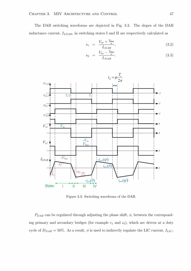
Chapter 3. MIV Architecture and Control 47
The DAB switching waveforms are depicted in Fig. 3.3. The slopes of the DAB
inductance current, ILDAB, in switching states I and II are respectively calculated as
s1 =Vin +
Vbus
n
LDAB
, (3.2)
s2 =Vin − Vbus
n
LDAB
. (3.3)
c1,4
c2,3
c6,7
c5,8
t
t
t
t
t
t
Vx1
Vx2
ILDAB
Vin
-VinVbus
-Vbus
TsTs/2
s1-s1
t
s2
-ipri(0)
-ipri(φ)
pj2
sd
Tt =
ipri(0)
ipri(φ)
I II III IVState:
-s2
Figure 3.3: Switching waveforms of the DAB.
PDAB can be regulated through adjusting the phase shift, ϕ, between the correspond-
ing primary and secondary bridges (for example c1 and c6), which are driven at a duty
cycle of DDAB = 50%. As a result, ϕ is used to indirectly regulate the LIC current, ILIC ,

Chapter 3. MIV Architecture and Control 48
to the reference, ILIC,ref , while MPPT or battery power control are achieved by regulating
Vin, or PDAB. This is obtained through adjusting the duty cycle of the LIC synchronous
boost converter, DLIC . This control process is illustrated in Fig. 3.2(b). These two inner
loop compensators are designed based on the separation of time constants; the bandwidth
of Gc1(s) is much lower than Gc2(s) to ensure stability.
3.2 DC-AC Stage
The dc-ac inverter stage consists of a soft-switching synchronous buck converter, followed
by a low-frequency unfolder full-bridge, as shown in Fig. 3.4(a). In grid-tied mode,
the high-voltage buck converter regulates the dc-link voltage, Vbus, while shaping the
Phase-Locked-Loop (PLL) synchronized grid current to achieve unity power factor, unless
reactive power support is needed. While in the nano-grid, the reference nano-grid current,
ig,ref (t) is generated by the droop functions. The inductor current, ILbuck, is regulated in
Boundary Conduction Mode (BCM) for soft-switching and high-efficiency [3]. At unity
power factor and P >0, the required on-time at time t, Ton(t), for the high-side switch is
Ton(t) = Lbuck∆I(t)
Vbus − |vg(t)|, (3.4)
where Lbuck is the buck converter inductance, and ∆I(t) is the current ripple of Lbuck at
time t. Similarly, the required Ton(t) for the low-side switch when P ≤ 0, and Q = 0 is
Ton(t) = Lbuck∆I(t)
|vg(t)|. (3.5)
The simplified control diagram for the dc-ac stage is shown in Fig. 3.4(b). Normalized
values for the on-time, Ton,nrm, throughout the half line-cycle are pre-calculated and
stored in a Look-Up Table (LUT), such that the average inductor current < ILbuck >Ts
is sinusoidal. Furthermore, normalized grid current values based on different Vbus and
nano-grid voltages are stored in a separate LUT. The reference grid current, ig,ref , is

Chapter 3. MIV Architecture and Control 49
Lbuck
Cbuck
Lfilter
+vg(t)-
c13 c16
c15 c14To dc-dcstage
c11
c12
ILbuck
+
Vbus
-
+
vgrid,rect(t)
-
Lfilter
Cfilter
(a)
+-
vg(t)
c15-16
c13-14
LUT 1 Free-wheeling
counterclk
reset
+-
Ton
ILbuck(t)
+
Ton,nrm
+
+-
c11
c12 DQILbuck
tT/2
TonMOD
MOD
|ig,ref(t)|
|ig,nrm(t)|
K
|)(|
)(
tv
tv
g
g
|)(|
)(
,
,
ti
ti
refg
refg
MOD==
LUT 2vg(t)
Vbus
ig(t)
Droop
Control
∆ILbuck
(b)
Figure 3.4: (a) Architecture and (b) simplified control diagram for the dc-ac stage.
used to determine the multiplier coefficient, K. Ton is determined by scaling the Ton,nrm
by this factor in order to achieve the P and Q targets.
3.3 Short-Term Storage
Battery or capacitor technology are viable options for this storage unit. While the bat-
teries suffer from short lifetime, specially under severe charge/discharge cycles, and tra-
ditional capacitors do not offer high energy density, Electric Double Layer Capacitors

Chapter 3. MIV Architecture and Control 50
(EDLC) are a compromise. EDLCs, also known as ultra-capacitors (u-caps), have a
symmetric input and output specific power in the range of 0.5-25 kW/kg [11], which is
at least 10× higher than typical Lithium-Ion (Li-Ion) batteries [12]. U-caps also offer
higher cycle-life, lower Equivalent Series Resistance (ESR) and reduced susceptibility to
high depth-of-discharge. A Lithium-Ion Capacitor (LIC) is a hybrid device that combines
the intercalation mechanism of traditional Li-Ion batteries with the cathode of EDLCs,
as shown in Fig. 3.5(a) [13]. The cathode exhibits an activated carbon material, while
charge is stored at the interface between the carbon and the electrolyte. The anode is
generally pre-doped with Lithium ions, resulting in a lower anode voltage, and a higher
cell voltage of 3.8-4 V versus 2.5-2.7 V for conventional EDLCs [13]. Unlike EDLCs, LICs
have a minimum operating voltage, VLIC,min. Overall, LICs have 2-4× higher energy den-
sity than EDLCs, as shown in Fig. 3.5(b). LICs are well suited as the distributed storage
units, where relatively high energy for power smoothing on the time-scale of minutes,
together with high cycle-life are required. Unlike batteries, LICs are expected to match
the required 20-25 year lifespan of PV systems.
3.4 Power Smoothing Algorithm
The short-term storage can be used to filter out the real power delivered or absorbed by
the converter, which in turn can improve the nano-grid power quality by reducing the
amount of power change in a time-unit, or dP/dt factor [15]. It can also lead to savings
on fuel costs for diesel generators in the conventional micro and nano-grids [16, 17],
where back-up gensets are used. The power smoothing feature can also be used to
filter out high spikes in batteries’ currents resulting in an improvement in the lifetime
of the batteries [18, 19]. A lag-free algorithm to achieve this feature in the MIV is
introduced based on predicted power prediction in this section. It is important to develop
a predictive approach with a limited storage capacity, as it helps mitigate the offset power

Chapter 3. MIV Architecture and Control 51
(a)
0.01
0.1
1
10
100
0.1 1 10 100 1000
Sp
ecific
Po
we
r (k
W/k
g)
Specific Energy (Wh/kg)
ucap 2.5 V
ucap 2.7 V
Battery discharge
Battery charge
LIC 3.8 V
EDLC U-capsBattery:Discharge
Battery:Charge
High-power batteries
High-energybatteries
LICs: Used in this work
(b)
Figure 3.5: (a) Physical structure of Lithium-Ion Capacitor [13]. (b) Ragone plot for different
storage technologies [14].
discrepancies due to the time delay between the original and smoothed power curves.
The smoothing process is illustrated in Fig. 3.6. Pin is sampled every 10 s and passed
to a moving averaging window of approximately 5 minutes, based on the low-latency Hull
digital filter [20], generating Pave. The LIC energy capacity for each MIV is chosen based
on providing/absorbing the rated inverter power for approximately 5 minutes, which

Chapter 3. MIV Architecture and Control 52
provides a sufficient buffer for startup and typical cloud variations.
At each sample point, the Least Square Estimation (LSE) method is used to generate
the polynomial s(θ) that best fits this curve, by finding the optimization vector variable
θ:
θ = argminθ
m∑n=1
(Pave(n)− s(n,θ))2, (3.6)
where m is the number of previous samples which are used for the prediction. In this
case, an averaging window of 5 minutes is considered, and thus m = 30, assuming that
the measurements are done every 10 s. To simplify the solution, it is generally assumed
that the signal (Pave in this case) can be modelled with a polynomial, in which case the
estimate s(θ) can be expressed as
s(θ) = Hθ, (3.7)
where H is any matrix of size m× (p + 1), while p is the order of polynomial which is
used in the estimation. In this work, p = 8 is chosen. A higher order polynomial increases
the prediction accuracy resulting in a smoother power curve; however the computation
effort and over-fitting risk increases substantially with p. A common expression for H is
as follows
Hm,p+1 =
1 1 · · · 1
1 21 · · · 2p
......
. . ....
1 m1 · · · mp
. (3.8)
It can be shown that θ = (HTH)−1HTP ave, and thus s(θ) can be constructed using
( 3.4). By evaluating s(m+ 1,θ), Pave(m+ 1) is forecasted. In order for PDAB to follow
the average power curve, the difference power, Pdiff , must be supplied or absorbed by
the LIC:
P ∗LIC(m+ 1) =
Pdiff
ηLICPdiff ≥ 0.
Pdiff .ηLIC Pdiff < 0,
(3.9)

Chapter 3. MIV Architecture and Control 53
where ηLIC is the LIC dc-dc converter efficiency, and P ∗LIC(m+ 1) is the calculated LIC
power reference at sample-time m+ 1. Pdiff is defined by the following
Pdiff = s(m+ 1,θ)− Pave(m+ 1). (3.10)
Vin
Iin
Hull
Moving
Averaging
PinLSE
Pave s(θ)
+
-
P*LIC
LIC SOC
Estimation
+
SOCref
Gc4(s)
+
I*LIC
I**LIC
ILIC,ref
Power Smoothing Loop
SOC Management Loop
+
To the LIC
Converter
LICV
1
-
Figure 3.6: Power smoothing and LIC SOC control.
A SOC management loop is implemented to gradually steer the LIC SOC to ≈50%
by generating the offset LIC current command, I∗∗LIC . The SOC is estimated by the LIC
voltage, by considering the well-known quadratic formula for stored energy of a capacitor,
E = 12CLICV
2LIC . The LIC’s capacitance is well maintained during its lifetime [13].
Maintaining the SOC near the mid-range is essential to maximize the potential swing.
The LIC current command at sample time m+ 1, is therefore
ILIC(m+ 1) =P ∗LIC(m+ 1)
VLIC
+ I∗∗LIC(m+ 1). (3.11)

Chapter 3. MIV Architecture and Control 54
3.5 Experimental Results
A 100 W MIV prototype was fabricated on a custom Printed Circuit Board (PCB) and
its operation was demonstrated. The prototype parameters are listed in Table 3.1. The
dc-dc and dc-ac stages are digitally controlled by an on-board FPGA and 16-bit micro-
controller, respectively. The DAB transformer was designed as a custom planar magnetic
element in order to limit the profile of the prototype to less than the thickness of a typical
PV panel.
Table 3.1: MIV Prototype Specifications
Parameter Value Units
Dc-Dc Stage Switching Frequency, fs 156 kHz
(DAB and LIC Converter)
Input Capacitance, Cin 450 µF
Bus Capacitance, Cbus 270 µF
Bus Voltage, Vbus 450 V
DAB Inductance, LDAB 4.7 µH
LIC Converter Inductance, LLIC 10 µH
Dc-Ac stage Inductance, Lbuck 500 µH
Transformer Turns Ratio, n 19
3.5.1 MIV Operation
The measured efficiency of the DAB, LIC and dc-ac stages are shown in Fig. 3.7. These
efficiency curves are nearly symmetrical and thus the data is shown only for the positive

Chapter 3. MIV Architecture and Control 55
75
80
85
90
95
100
0 20 40 60 80 100 Efficiency (%
) Power (W)
DAB Converter
Dc-ac stage
LIC Converter
Figure 3.7: Measured efficiency of the DAB, LIC and dc-ac stages.
c5
c2
ILDAB
ᵩ Ts
DAB
buspv
L
n
VV +
DAB
buspv
L
n
VV +-
Figure 3.8: Steady-state waveforms for the DAB converter (ILDAB:5 A/div).
power flow. The converter stages achieve a peak efficiency of 95.1%, 97.2%, and 96.3%,
for DAB, LIC and dc-ac stages, respectively.
The steady-state DAB waveforms at the rated power of 100 W are shown in Fig.3.8.
The dynamic response of the PV voltage regulation loop for a step change in Vpv,ref and
ILIC,ref are shown in Fig. 3.9(a) and (b), respectively. In both cases, ILIC and Vin keep
well regulated to their respective reference values, mitigating the disturbance induced by
the other control loop. The dynamic response of a battery inverter to consecutive step
changes in P ∗, while Q = 0, is shown in Fig. 3.10.
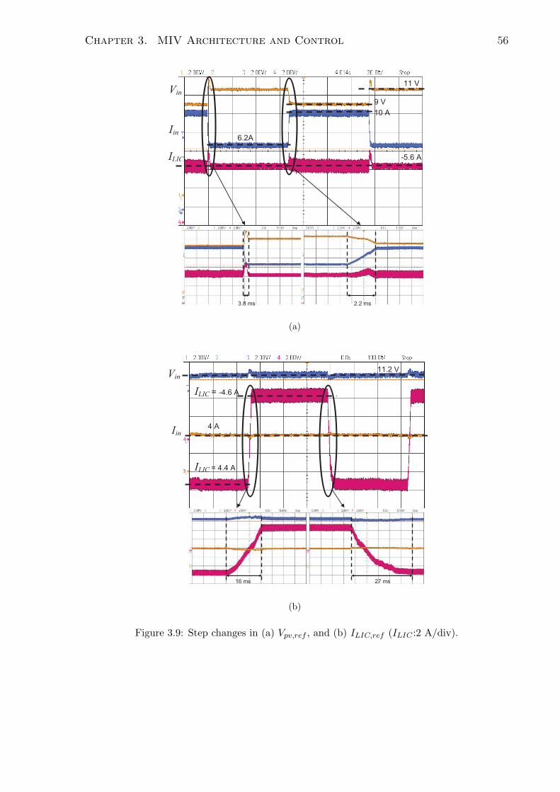
Chapter 3. MIV Architecture and Control 56
Vin
Iin
ILIC
11 V
9 V
10 A
6.2A
-5.6 A
3.8 ms 2.2 ms
(a)
ILIC = -4.6 A
Iin
Vin11.2 V
4 A
ILIC = 4.4 A
16 ms 27 ms
(b)
Figure 3.9: Step changes in (a) Vpv,ref , and (b) ILIC,ref (ILIC :2 A/div).

Chapter 3. MIV Architecture and Control 57
Vgrid
Igrid
678 V
0.22 A 0.6 A
Figure 3.10: MIV dynamic response at unity power factor with two consecutive P steps, 40 W
→ 16 W → 40 W (Ig:0.2 A/div).
3.5.2 Smoothing Algorithm Performance Evaluation
The smoothing process was demonstrated using a Building-Integrated PV module (BIPV)
as the input. The measured power curve of the BIPV module is shown in Fig. 3.11(a).
A relatively cloudy day was chosen to illustrate the power smoothing process. The test
was run on November 16, 2013, for a rooftop installation at the University of Toronto.
The activation of the PV module’s internal sub-string bypass diodes at the start of the
day is clearly visible, leading to fast variations in power at sunrise. The power smoothing
algorithm depicted in Fig. 3.6 was separately implemented on a PC running NI LabVIEW,
allowing a flexible choice of filtering parameters, while all other controls are implemented
locally in the micro-controller and FPGA. Two 4.4 Wh LICs are connected in series,

Chapter 3. MIV Architecture and Control 58
Table 3.2: LIC and PV Specifications
Parameter Value Units
Nominal MPPT PV Voltage, Vmpp 10 V
Nominal MPPT PV Current, Impp 10 A
Total Minimum LIC Voltage, VLIC,min 4.4 V
Total Maximum LIC Voltage, VLIC,max 7.6 V
Total LIC Capacitance, CLIC 2200 F
Total LIC Energy Capacitance, ELIC 8.8 Wh
# of Series-Connected LIC Modules 2
resulting in a voltage range of 4.4 V≤ VLIC ≤7.6 V. The specifications for the PV and
LICs used in this experiment are listed in Table 3.2. The net generated power, P , is
approximately 7× smoother than Pin, as shown in Fig. 3.11(b). The LIC voltage swing
throughout the cloudy day is shown in Fig. 3.11(c), which demonstrates the proper sizing
of the storage module for the considered averaging period. The slow SOC regulation
loop correctly steers the LIC voltage towards 6.2 V throughout the day. The level of
smoothing can be increased by tuning the filter parameters to utilize a wider range of
the LIC’s capacity. There is clearly a trade-off between the amount of power smoothing
and the energy yield of the inverter module, based on the LIC converter efficiency.

Chapter 3. MIV Architecture and Control 59
6 7 8 9 10 11 12 13 14 15 16 17 18−20
−10
0
10
20
30
40
50
60
70
80
90
100
t
Po
we
r (W
)
Ppv
s(θ)
Ppv,ave
PLIC
(hour)
(a)
6 7 8 9 10 11 12 13 14 15 16 17 18−4−3−2−1012345678
t
dP/dt(W/s)
dPpv/dt
ds(θ)/dt
(hour)
(b)
6 7 8 9 10 11 12 13 14 15 16 17 185.25.35.45.55.65.75.85.9
66.16.26.36.46.56.66.7
t
VL
IC (
V)
(hour)
SOC = 50%
(c)
Figure 3.11: (a) PV power, Ppv, the running average, Ppv,ave, the fitted polynomial, s(θ), and
the LIC power, PLIC . (b)dPdt ,
ds(θ)dt , and (c) VLIC for a typical cloudy day.

Chapter 3. MIV Architecture and Control 60
3.6 Chapter Summary
A two-stage, four-quadrant MIV architecture and simple control scheme were developed
for the modular low-cost nano-grid application. The two-stage MIV architecture is com-
prised of a dc-dc and a dc-ac stage:
1. The dc-dc stage consists of a DAB converter connecting the PV/battery to the high
voltage dc-link, as well as a boost converter interfacing an extra short-term storage
element.
2. The dc-ac stage consists of a buck converter succeeded by an active unfolder.
The MIV architecture features the integration of LIC technology as the short-term stor-
age. The LIC technology exhibits the extended lifetime of ultra-capacitors, which matches
well with the expected lifetime of the PV modules, while demonstrating an order of mag-
nitude higher energy density.
Stable MIV operation was achieved by incorporating a dual loop approach in the dc-
dc stage. The DAB indirectly regulates the LIC’s current, while MPPT/battery power
regulation is achieved by the LIC dc-dc converter. The four-quadrant dc-ac stage operates
in BCM current control which ensures a high efficiency of up to 96.3%.
A lag-free averaging scheme was introduced which decreases the real power variations
of a PV inveter by up to 7× on a typical cloudy day by utilizing the short-term storage.
This benefits the stability of the nano-grid while saving on fuel and maintenance costs and
improving generator lifetime, if a conventional generator is used in the system. There is an
inherent trade-off between the degree of power smoothing and the MIV overall efficiency;
more processed power in the LIC converter results in more filtering and smoother power
generation.

References
[1] S. Poshtkouhi, M. Fard, H. Hussein, L. Dos Santos, O. Trescases, M. Varlan, and
T. Lipan, “A dual-active-bridge based bi-directional micro-inverter with integrated
short-term Li-Ion ultra-capacitor storage and active power smoothing for modu-
lar PV systems,” in IEEE Applied Power Electronics Conference and Exposition
(APEC), March 2014, pp. 643–649.
[2] S. Kjaer, J. Pedersen, and F. Blaabjerg, “A review of single-phase grid-connected
inverters for photovoltaic modules,” IEEE Transactions on Industry Applications,
vol. 41, no. 5, pp. 1292–1306, Sept 2005.
[3] R. Erickson and D. Maksimovic, Fundamentals of Power Electronics, Second Ed.
Springer, 2001.
[4] J. Salmon, A. Knight, and J. Ewanchuk, “Single phase multi-level pwm inverter
topologies using coupled inductors,” in IEEE Power Electronics Specialists Confer-
ence (PESC), June 2008, pp. 802–808.
[5] Z. Wang and H. Li, “An integrated three-port bidirectional dc-dc converter for pv
application on a dc distribution system,” IEEE Transactions on Power Electronics,
vol. 28, no. 10, pp. 4612–4624, 2013.
[6] F. Krismer and J. Kolar, “Efficiency-optimized high-current dual active bridge con-
verter for automotive applications,” IEEE Transactions on Industrial Electronics,
vol. 59, no. 7, pp. 2745–2760, 2012.
61

REFERENCES 62
[7] H. Qin and J. Kimball, “Generalized average modeling of dual active bridge dc-dc
converter,” IEEE Transactions on Power Electronics, vol. 27, no. 4, pp. 2078–2084,
2012.
[8] W. Chen, P. Rong, and Z. Lu, “Snubberless bidirectional dc-dc converter with new
cllc resonant tank featuring minimized switching loss,” IEEE Transactions on In-
dustrial Electronics, vol. 57, no. 9, pp. 3075–3086, Sept 2010.
[9] Y.-C. Wang, Y.-C. Wu, and T.-L. Lee, “Design and implementation of a bidirec-
tional isolated dual-active-bridge-based dc/dc converter with dual-phase-shift con-
trol for electric vehicle battery,” in IEEE Energy Conversion Congress and Exposi-
tion (ECCE), Sept 2013, pp. 5468–5475.
[10] D. Costinett, K. Hathaway, M. Rehman, M. Evzelman, R. Zane, Y. Levron, and
D. Maksimovic, “Active balancing system for electric vehicles with incorporated
low voltage bus,” in IEEE Applied Power Electronics Conference and Exposition
(APEC), March 2014, pp. 3230–3236.
[11] “48 V ultra-capacitor specifications,” Maxwell Technologies Inc. datasheet, 2011,
available at http://maxwell.interconnectnet.com/ultracapacitors/datasheets/datasheet/48V/series/1009365.pdf.
[12] “U-Charge Xp Lithium Iron Magnesium Phospate Battery,” Valence Technology
datasheet, 2010, available at http://www.valence.com/energy-storage/xp-12v-19v-
lithium-phosphate-battery-module.
[13] “Lithium-Ion Capacitor,” JSR Micro, 2012, available at
http://www.jsrmicro.com/index.php/EnergyAndEnvironment/.
[14] O. Laldin, M. Moshirvaziri, and O. Trescases, “Predictive algorithm for optimiz-
ing power flow in hybrid ultracapacitor/battery storage systems for light electric
vehicles,” IEEE Transactions on Power Electronics, vol. 28, no. 8, pp. 3882–3895,
2013.

REFERENCES 63
[15] M. Datta, T. Senjyu, A. Yona, T. Funabashi, and C.-H. Kim, “A frequency-control
approach by photovoltaic generator in a pv-diesel hybrid power system,” IEEE
Transactions on Energy Conversion, vol. 26, no. 2, pp. 559–571, 2011.
[16] J.-H. Lee, S.-H. Lee, and S.-K. Sul, “Variable-speed engine generator with superca-
pacitor: Isolated power generation system and fuel efficiency,” IEEE Transactions
on Industry Applications, vol. 45, no. 6, pp. 2130–2135, 2009.
[17] M. Datta, T. Senjyu, A. Yona, T. Funabashi, and C.-H. Kim, “A coordinated control
method for leveling pv output power fluctuations of pv-diesel hybrid systems con-
nected to isolated power utility,” IEEE Transactions on Energy Conversion, vol. 24,
no. 1, pp. 153–162, 2009.
[18] L. Shao, M. Moshirvaziri, C. Malherbe, A. Moshirvaziri, A. Eski, S. Dallas, F. Hur-
zook, and O. Trescases, “Ultracapacitor/battery hybrid energy storage system with
real-time power-mix control validated experimentally in a custom electric vehicle,” in
IEEE Applied Power Electronics Conference and Exposition (APEC), March 2015,
pp. 1331–1336.
[19] J. Blanes, R. Gutierrez, A. Garrigos, J. Lizan, and J. Cuadrado, “Electric vehicle
battery life extension using ultracapacitors and an fpga controlled interleaved buck-
boost converter,” IEEE Transactions on Power Electronics, vol. 28, no. 12, pp.
5940–5948, Dec 2013.
[20] “Hull Moving Average (HMA),” Alan Hull, available at
http://www.justdata.com.au/Journals/AlanHull/.

Chapter 4
DAB Converter: Drawbacks and
Enhancements
A typical PV generation system spends more than two-thirds of the time operating below
50% of its rated power [1]. It is therefore desirable to operate the MIV in an alternate
low-power mode in order to maintain high efficiency over a broad power range. This
is crucial in any commercial MIV architecture; for example the European Efficiency
index dedicates 32% of the total evaluation weight to operation below 30% of the rated
power [2]. In addition, the implementation cost of the MIV needs to be reduced, while its
reliability has to be increased in order to match the lifetime expectancy of PV modules.
The DAB topology is utilized as the core of the dc-dc stage in the developed MIV
architecture introduced in Chapter 3. Despite the attractive features of this topology,
there are two main inherent drawbacks to it:
1. The conventional DAB converter suffers from relatively poor efficiency at low power
due to the loss of ZVS and extended drive losses of its high number of active
switches [3]. In addition, the regulation accuracy is compromised at low-power
levels, as proven in Section 4.1.2. This issue can be addressed by operating at
other switching modes at these power levels and performing Bus Voltage Scaling
64

Chapter 4. DAB Converter: Drawbacks and Enhancements 65
(BVS), which can be done as an extra degree of freedom in two-stage MIVs. These
methods are discussed in detail in Section 4.1.
2. Due to the presence of active switches on both sides of the galvanic isolation in
the dc-dc stage, the gating signals have to be sent from the controller side to the
other side using multiple digital isolators. Digital isolators are typically needed for
data communication between the dc-dc and dc-ac stages as well. This results in
extra cost and more power consumption, while compromising the reliability of the
MIV by adding potential points of failure. This is particularly more important in
low-power, high-frequency converters designed for low-cost PV applications. New
methods have to be developed in order to mitigate the need for such devices. This
issue is addressed in Section 4.2.
4.1 Low-Power Efficiency Enhancement
A general design method for conventional DAB mode operation based on frequency op-
timization is introduced in [3]. Switching frequency optimization results in limited effi-
ciency improvements at low power. Higher efficiency are achieved by utilizing burst-mode
operation, which has been recently proposed in [4, 5]; however this method leads to in-
creased input voltage ripple for PV inverters, which is detrimental to MPPT efficiency.
By slightly modifying the conventional DAB topology, a new Flyback-based mode of
operation can be achieved, which is discussed in the following section.
4.1.1 Modified DAB Architecture and Principle of Operation
The modified DAB topology is shown in Fig. 4.1(a). This converter is a modified DAB
that interfaces Vin with the dc link, Vbus, and utilizes one more switch, M7b in one of the
secondary legs.

Chapter 4. DAB Converter: Drawbacks and Enhancements 66
DAB Mode
The switching waveforms of the modified DAB converter are shown in Fig. 3.3. In
two-stage MIV architectures, Vbus is generally regulated to a fixed voltage. The reference
voltage, Vbus,ref , is usually chosen to optimize efficiency at the nominal operating point [1].
It can be shown that the DAB converter achieves turn-on ZVS and maximum efficiency
when Vbus = nVin, as the reactive circulating current is minimized [3]. The switching
waveforms of the DAB converter with optimized Vbus are shown in Fig. 4.2(a). Meeting
this condition leads to s2 = 0, which is the slope of ILDAB during State II, thereby
resulting in full free-wheeling in ILDAB during this state. In order to minimize the losses
in the DAB, the reference for the dc-link voltage, Vbus,ref , is dynamically adjusted such
that Vbus,ref = nVin. For PV inverters, it is well-known that the MPP voltage undergoes
a relatively low fluctuation of about 30% during the course of a typical day [6]. This is
in contrast to the PV current at MPP, IMPP , which is proportional to irradiance and
thus has large-scale fluctuations, especially on cloudy days. Vin has slow dynamics for
battery inverters as well, which is desirable in terms of the dc-link voltage adjustment
bandwidth.
Flyback Mode
By driving M1 and M4 simultaneously on the primary-side, the converter can be operated
similar to a conventional two-transistor flyback converter (2T-flyback) [7]. The switch
configuration in Flyback mode is shown in Fig. 4.1(b). The switches M1 and M4 remain
active, M8 is kept on and all other switches are off. The secondary-side bridge is modified
by adding one switch, M7b, to achieve bidirectional blocking capability in the Flyback
mode. The rising and falling slopes of the magnetizing inductance current, ILm , are given

Chapter 4. DAB Converter: Drawbacks and Enhancements 67
LDAB 1:n Cbus
+
Vin
-
Lm
+
Vbus
-
ILDAB
ILm+Vx1-
+Vx2-
ID
Cin
+ VLDAB -M1 M2
M3 M4
M5 M6
M8M7
M7b
Iin
Primary Side Secondary Side
(a)
LDAB 1:n Cbus
+
Vin
-
Lm
+
Vbus
-
ILDAB
ILm+Vx1-
+Vx2-
ID
Cin
+ VLDAB -M1 M2
M3 M4
M5 M6
M8M7
M7b
OFF
ON
Switching
Iin
(b)
Figure 4.1: a) Proposed modified DAB dc-dc topology for improved low power efficiency. b)
Switch configuration in Flyback mode.
by
s3 =Vin
LDAB + Lm
, (4.1)
s4 =−Vbus
nLm
. (4.2)
The DAB inductance circulates energy in every switching period in this mode. The
rising slope of ILDAB is the same as s3 and the falling slope is
s5 =−Vin − Vbus
n
LDAB
. (4.3)

Chapter 4. DAB Converter: Drawbacks and Enhancements 68
c1,4
c2,3
c6,7
c5,8
t
t
t
t
t
t
Vx1
Vx2
ILDAB
Vin
-VinVbus=nVin
-Vbus
TsTs/2
s1-s1
t
s2=0
-ipri(0)
-ipri(φ)
pj2
sd
Tt =
ipri(0)
ipri(φ)
I II III IVState:
(a)
c1,4
c2,3,5-7
Ton=
D1Ts
t
t
t
ILDAB
ILm
Ts
t
t
ID
D2Ts
s3
s3 s5
s4
s7s6
Circulating
Charge
t
c8
sssssss3333sssss
I
II
III IVState:
(b)
Figure 4.2: Switching waveforms in (a) DAB mode with optimized DC-link voltage (Vbus =
nVin), and (b) Flyback mode.

Chapter 4. DAB Converter: Drawbacks and Enhancements 69
Finally, the output diode current, ID, delivers charge to the bus with the following slopes
in switching states II and III
s6 =s4 − s5
n, (4.4)
s7 =s4n. (4.5)
The 2T-flyback topology exhibits several advantages over DAB mode for low power
conditions, including lower switching and gate-drive losses (two switching devices versus
nine in the DAB mode). Unlike the more conventional single transistor flyback topology,
the body diodes of M2 and M3 clamp the drain voltage on M1 and M4, which limits the
blocking voltage rating on the primary switches to Vin. The Flyback mode is operated
with fixed on-time, Ton, in Pulse Frequency Modulation (PFM) mode [8], where Ton is
given by
Ton = D1Ts, (4.6)
D1 is the duty cycle in Flyback mode, and Ts is the switching period.
The corresponding converter waveforms are shown in Fig. 4.2(b). There are two
inherent limitations to the 2T-flyback topology:
1. D1 must be less than 50% in order to avoid transformer saturation.
2. Vbus must be less than nVin, to ensure that the body diode of M5 transfers power to
Vbus when the primary-side switches are off. As a result, Vbus needs to be reduced
in Flyback mode.
The presence of LDAB, which is not required in the 2T-flyback topology, results in
additional losses, since it circulates current in a switching period. The energy captured
in LDAB is transferred back to the input capacitance, Cin, in the 2T-flyback topology, as
opposed to a conventional flyback scheme, which does not provide a return path for the

Chapter 4. DAB Converter: Drawbacks and Enhancements 70
energy absorbed by the leakage inductance. In addition, LDAB results in the soft turn-on
of the output diode.
The Flyback mode exhibits unidirectional power transfer. The converter can operate
with reverse power flow by adding another switch on the primary-side. This additional
switch is not included in the experimental prototype, as the efficiency in DAB mode
is sensitive to conduction losses at the low-voltage, high-current primary-side. While
possible, reverse power capability is not strictly needed in low-power Flyback mode; the
DAB can be prevented from operating in this condition by adopting burst-mode control
instead, albeit at slightly lower efficiency than Flyback mode.
Dual Mode Control
The conceptual control diagram for a stand-alone DAB converter, without any interface
to short-term storage, is shown in Fig. 4.3. In this case, the phase-shift ϕ is used to
directly control the power-flow, PDAB. c1−8 denote the gating voltages for switches M1−8.
The DAB mode is adopted if PDAB is higher than a threshold value, Pthresh, or if PDAB
is negative, in which case the storage is charged directly from the bus. In DAB mode,
ϕ is controlled to regulate the power-flow to/from the dc-ac stage, based on MPPT or
the desired power target, for PV and battery inverters respectively. In Flyback mode,
Ts is adjusted by the controller, Gc2(s), in order to regulate PDAB to the reference P ∗.
Assuming that the magnetizing inductance of the transformer, Lm, is much larger than
LDAB, the power-flow is given by
PDAB =(VinD1)
2Ts
2Lm
. (4.7)
4.1.2 Regulation Accuracy at Low Power
In the following analysis it is shown that the power regulation accuracy is greatly im-
proved by operating in Flyback mode at low power levels. In turn, this alleviates the
potential for limit-cycle oscillations. Limit-cycle oscillations are commonly observed in

Chapter 4. DAB Converter: Drawbacks and Enhancements 71
c’5-8
clk
reset
+
P*
φ c’1-4
Ton
c’5-8
φ c’1-4
clkll
reset
ToTT n
DAB mode
Flyback mode
Ts
M
U
X
Mode
Selector
-PDAB
c’1-8
Gc2(s) +-
Free-wheeling
counter
c”1
c”2
c”3-7
c”8
c”1-8
c1-8
Enable (en)Condition
threshDAB PP ££0
0<DABP
DABthresh PP <
1 (DAB Mode)
1 (DAB Mode)
0 (Flyback Mode)
en
+-
Gc1(s)
PWM
Phase-Shift
0
Figure 4.3: Simplified conceptual control diagram of the modified DAB converter.
digitally controlled SMPS based on the quantizer resolutions, whether in current-mode [9]
or voltage-mode control [10].
The power versus time-shift, td, of a DAB converter with switching frequency, fs =
195 kHz, is shown in Fig. 4.4(a). The plot includes the theoretical prediction from the
DAB ideal power-flow equation, as well as the simulated result for a non-ideal converter
having the same specifications.
The ideal incremental power versus time-shift, dPDAB
dtd, is also shown in the same figure,
which peaks at PDAB=0. Namely
dPDAB
dtd= − td
|td|VinVbus
nωsLDAB
(2π
Ts
)(1− 4
Ts
|td|). (4.8)
This results in a nonlinear incremental power versus phase-shift profile in the DAB mode,
with the regulation accuracy being worse in the low-power region. In Flyback mode, the
converter operates with variable switching frequency, fs = 1/Ts. The power versus Ts
is shown in Fig. 4.4(b) for both the ideal case based on (4.7) and simulated converter
considering the conduction losses. The ideal dPDAB
dTsfactor in this mode is given by
dPDAB
dTs
= −(VinTon)2
2LmTs2 . (4.9)

Chapter 4. DAB Converter: Drawbacks and Enhancements 72
−1.5 −1 −0.5 0 0.5 1 1.5−150
−100
−50
0
50
100
150
td (µs)
PD
AB (
W)
−1.5 −1 −0.5 0 0.5 1 1.50
5
10
15
20
25
30
dPDAB
/dtd (W/µs)
Ideal PDAB
(W)
Simulated PDAB
(W)
dPDAB
/dtd
(W/µs)
(a)
20 25 30 35 40 45 505
10
15
20
25
30
35
40
45
Ts (µs)
PD
AB (
W)
20 25 30 35 40 45 50−4
−3.5
−3
−2.5
−2
−1.5
−1
−0.5
0dP
DAB/dT
s (W/µs)
Ideal PDAB
(W)
Simulated PDAB
(W)
dPDAB
/dTs
(W/µs)
(b)
Figure 4.4: (a) PDAB and dPDABdtd
in DAB mode, and (b) PDAB and dPDABdTs
in Flyback mode.

Chapter 4. DAB Converter: Drawbacks and Enhancements 73
The incremental power in Flyback mode has the opposite trend compared to DAB
mode; dPDAB/dTs is less at low power levels, which improves the accuracy of the power
regulation loop.
Based on a time resolution of 20 ns for a 50 MHz clock frequency, and according to
Fig. 4.4, a single LSB increase in td at PDAB = 6 W results in a 50 mW (0.8%) increase
in PDAB in Flyback mode. However, the same LSB increase in DAB mode results in
480 mW (8%) increase in PDAB, which corresponds to more than 3 bits of reduction
in the effective control resolution. Dual mode operation therefore benefits not only the
efficiency, but also the control performance.
4.1.3 Transformer Design
The transformer designed for dual-mode operation is shown in Fig. 4.5(a). The 3C95
Ferrite material has low core losses up to 100C [11]. The typical magnetic flux density
versus magnetic field for this material is shown in Fig. 4.5(b). Assuming a gap-less core,
the transformer in DAB mode exhibits the following peak magnetic flux density which is
independent of the power level
Bpeak =1
4Acn2
Vbus,dab · Ts,dab, (4.10)
where Ac is the core’s cross sectional area, Ts,dab is the switching period in DAB mode,
Vbus,DAB is the dc link voltage in DAB mode and n2 is the number of turns on the
secondary winding of the transformer. Assuming that LDAB ≪ Lm, Bpeak in Flyback
mode depends on Ton and is given by
Bpeak =1
Acn1
Vin · Ton, (4.11)
where n1 is the number of turns on the primary winding of the transformer. Comparing
(4.10) and (4.11), the maximum on-time in Flyback mode is limited to
Ton ≤ 1
4n
Vbus,dab
Vin
Ts,dab, (4.12)

Chapter 4. DAB Converter: Drawbacks and Enhancements 74
38 mm
32.65 mm12.25
mm
(a) (b)
Figure 4.5: (a) Planar transformer used in this work for dual-mode operation, and (b) typical
B-H curve for C95 magnetic material [11].
such that peak flux density does not exceed the value from DAB mode. For example if
Vbus,dab = nVin, and Ts,dab = 5.12 µs, the maximum Ton is 1.28 µs. Replacing (4.12) in
(4.7), and considering the fact that D1 ≤ 0.5 and Vbus,dab = nVin, the maximum power
transfer in Flyback mode is therefore given by
Pfl,max =V 2inTs,dab
16Lm
. (4.13)
In practice, the transformer in a DAB converter is designed to limit the core losses at
the rated power and maximum frequency, which results in the saturation flux density of
the material being well above Bpeak from (4.10). As a result, it is possible to increase
Ton substantially higher than predicted by (4.12) for the Flyback operation at low power
and low frequency, without resorting to a gapped core. A Ton value of 8 µs is used to
achieve Pthresh = 40 W in Flyback mode without introducing an air gap into the core.
The maximum on-time suggested by (4.12) is 1.28 µs, hence the core operates with a

Chapter 4. DAB Converter: Drawbacks and Enhancements 75
significantly higher Bpeak in Flyback mode.
4.1.4 Efficiency Analysis
This section discusses the dominant power losses in the DAB and Flyback modes. An
approximate loss analysis is useful to evaluate the threshold reference power value, Pthresh.
Conduction Losses
As shown in Fig. 3.3(a), the current into the leakage inductance and primary winding of
the transformer approach a perfect trapezoid when Vbus = nVin. The following equation
for the RMS current at the primary-side of transformer, Ipri, can be obtained from [12]
Ipri =1
3π(ipri(0)
2γ + ipri(ϕ)2(ϕ− γ)
+(π − ϕ)(ipri(0)2 + ipri(ϕ)
2 − ipri(0)ipri(ϕ)), (4.14)
where
γ =ipri(0)
ipri(0)− ipri(ϕ), (4.15)
and ipri(0) and ipri(ϕ) are the instantaneous currents of the transformer at the primary-
side at times t = 0 and t = ϕωs, respectively. These can be easily calculated considering
the symmetry of the transformer current [12]
ipri(0) =1
2LDABωs
(πVin − (π − 2ϕ)Vbus
n), (4.16)
ipri(ϕ) =1
2LDABωs
((π − 2ϕ)Vin − πVbus
n). (4.17)
Similar calculations can be done for the transformer’s secondary-side RMS current,
Isec. Two primary and two secondary switches are conducting at each instance in DAB
mode. Thus, the conduction losses in this mode are approximated by
PDAB,cond = (2Ron,pri +RLDAB)I2pri + (4.18)
2.5Ron,secI2sec,

Chapter 4. DAB Converter: Drawbacks and Enhancements 76
where Ron,pri and Ron,sec are the primary and secondary-side switches’ on-resistances
respectively, and RLDABis the lumped winding resistance of the transformer and inductor.
The factor of 2.5× on the secondary-side comes from the fact that there are two back-
to-back switches, M7, and M7b on one leg in the secondary-side to support the Flyback
operation. All five switches on the secondary-side are chosen to be identical. This results
in a slightly asymmetrical voltage on the transformer taps during one switching cycle in
the DAB mode. The on-resistance of the MOSFETs used in the secondary-side of the
converter have a relatively high positive temperature coefficient. The resulting thermal
feedback mechanism helps to avoid transformer saturation or significant DC magnetizing
flux in the transformer in DAB mode.
Neglecting the clamping diodes’ conduction interval, the RMS current for the two
switches, IM1,M4 , and in the output diode, D, in the 2T-flyback converter can be obtained
as [13]
IM1,M4 =nPDAB
√D1
Vbus(1−D1), (4.19)
ID =D2TsVbus
n2Lm
√D2
3, (4.20)
where D2 is approximated by
D2 =nVinD1
Vbus
. (4.21)
The total conduction loss in Flyback mode is
PFlbk,cond = (2Ron,pri +RLDAB)I2M1 + (4.22)
VF ID +Ron,secI2D,
where VF is the output diode’s forward voltage.

Chapter 4. DAB Converter: Drawbacks and Enhancements 77
Switching Losses
The switches in DAB mode can be turned on realizing Zero Voltage Switching (ZVS) [12].
However the turn-off losses are not fully eliminated. Assuming the output capacitance of
MOSFETs is small enough, the total switching losses in this mode can be approximated
by
PDAB,sw =1
2fstoff (Vin(ipri(0) + ipri(ϕ) + (4.23)
Vbus(isec(0) + isec(ϕ)),
where toff is the turn-off time of the MOSFETs.
Switches M1 and M2 exhibit hard switching at turn-off in Flyback mode. Thus, the
corresponding switching loss in Flyback mode can be approximated as
PFlbk,sw =V 2inD1toff
2(LDAB + Lm). (4.24)
The gate-driver losses are not analyzed here in detail, however there are nine active
switches in DAB mode compared to only two in Flyback mode. Considering that fs is
lower in Flyback mode, the overall gate-driver losses are drastically reduced.
Core Losses
Core losses are present in the high-frequency transformer and external inductor LDAB
in both DAB and Flyback modes. These losses can be roughly approximated using the
basic Steinmetz equation [14]
Pcore = kfαs B
βpeak, (4.25)
where Bpeak is the peak flux density, and k, α, and β are the Steinmetz parameters,
which depend on the core material. Core losses constitute a relatively low percentage of

Chapter 4. DAB Converter: Drawbacks and Enhancements 78
0
0.2
0.4
0.6
0.8
1
1.2
1.4
1.6
1.8DAB
Flyback
PDAB = 10 W
PowerLoss(W)
Conduction Switching Core
(a)
0
0.5
1
1.5
2
2.5
3
3.5DAB
Flyback
PDAB = 40 W
PowerLoss(W)
Conduction Switching Core
(b)
Figure 4.6: Simulated power losses for (a) P = 10 W, and (b) P = 40 W.
the total losses in DAB mode [12] due to high-frequency ac-ac operation. However, core
losses are dominant in Flyback mode due to the magnetizing inductance waveform. This
simplified analysis neglects the skin effect in all conductors, which can be significant,
especially in DAB mode due to high frequency operation.
Loss Comparison in Two Modes
The calculated loss breakdown for the two power levels, PDAB = 10 W and PDAB = 40 W,
is shown in Fig. 4.6. The considered prototype specifications are listed in Table 4.1. The
conduction losses in all active and passive elements are lumped together. The switching
losses also include the drive losses. In Flyback mode, the switching losses are reduced
by at least 10×, mostly by eliminating the turn-off losses on the high-voltage side, at a
cost of marginal increase in conduction losses. The transformer and inductor core loss is
slightly higher in Flyback mode, due to higher Bpeak. The core losses in Flyback mode
increase rapidly with the power due to higher Bpeak and fs. This is not the case for the
DAB converter, in which the core losses remain almost constant over the full phase shift
range due to constant Lm excitation based on (4.10) [15].

Chapter 4. DAB Converter: Drawbacks and Enhancements 79
4.1.5 Simulation and Experimental Results
A prototype of the system shown in Fig. 4.1(b) was fabricated on a custom Printed
Circuit Board, with power rating of 100 W. The main specifications of the prototype
are listed in Table 4.1. A minimum frequency of 20 kHz is adopted in Flyback mode to
avoid interfering with the audible range, while a fixed frequency of 195 kHz is adopted
for DAB mode. The DAB converter can be operated with lower frequencies without
saturating the magnetic cores, however, reducing the switching frequency increases RMS
currents in the converter. Furthermore, the turn-off process happens at higher current
values and thus the total switching losses do not scale down linearly with frequency. For
example, reducing the switching frequency by 50% increases the RMS current in primary,
secondary and active devices by about 38% at PDAB = 70 W, which translates into ≈90%
more conduction losses, while the total switching losses are reduced by 22%.
The converters are digitally controlled using an on-board FPGA. A custom planar
transformer shown in Fig. 4.5(a) was designed to reduce the weight and profile of the
prototype. The sub-optimal general operation of the DAB converter without dynamic
Vbus scaling is shown in Fig. 4.7 (a). The steady-state waveforms in DAB mode with
bus voltage scaling (Vbus = nVin) and Flyback mode at PDAB = 70 W, and PDAB = 15
W, are shown in Fig. 4.7(b) and (c) respectively. There are two interesting phenomena
which are noticeable in Flyback mode. First, the oscillations which are observed on the
voltage across the DAB inductance, VLDAB, are due to the resonance of LDAB with the
output capacitance of the MOSFETs on the primary-side and the capacitance on the
transformer’s primary winding. Second, ILDAB has two distinct rising slopes. The rising
slope following turn-on is large, then reduces to s3, as shown in the ideal waveforms in
Fig. 3.3(b). This happens when Lm is not fully demagnetized by the start of the switching
cycle in Flyback mode. This effect is shown in Fig. 4.8 when the Flyback is operating
in Continuous Conduction Mode (CCM). The initial rising slope of ILDAB, is equal to s1
from (3.1).

Chapter 4. DAB Converter: Drawbacks and Enhancements 80
44 V
7 V
-44 V
-VLDAB
-ILDAB5.5 A
-5.5 Ac8
c4
-7 V
-5 A
5 A
(a)
44 V
0 V
-44 V
VLDAB
-ILDAB 5.5 A
-5.5 A
c8
c4
(b)
8 A
ILDAB
Vbus
170 V
-VLDAB
c4
(c)
Figure 4.7: Steady-state waveforms of the converter in (a) DAB mode without dynamically
adjusted DC link voltage, (b) DAB mode with adjusted DC link voltage (Vbus = n Vin) at Vin
= 22 V (ILDAB:5 A/div), and (c) Flyback mode at Vin = 25 V (ILDAB:5 A/div).

Chapter 4. DAB Converter: Drawbacks and Enhancements 81
Table 4.1: Dual Mode DAB Converter Prototype Specifications
Parameter Value Unit
Rated Power, Pnom 100 W
Dc-dc Stage Switching Frequency, fs
DAB Mode 195 kHz
Flyback Mode 20-50 kHz
Fixed On-Time, Ton 8 µs
Input Capacitance, Cin 300 µF
Bus Capacitance, Cbus 100 µF
DAB Inductance, LDAB 4.2 µH
Magnetizing Inductance, Lm 32 µH
Bus Voltage Range, Vbus
DAB mode 200-270 V
Flyback mode 170 V
Transformer Turns Ratio, n 9
Based on Fig. 4.5(b), Lm increases significantly at low magnetizing currents. This
prevents the full demagnetization of Lm in one switching cycle. As a result, ILm has a
minimum value of about 1 A. This effect can be mitigated by introducing an air gap in
the transformer. This will reduce the reluctance of the core and linearize Lm for the full
operating range. The closed-loop dynamic response of Flyback mode for a step change
in P ∗, while the dedicated integrated storage converter is off, is shown in Fig. 4.9. fs is

Chapter 4. DAB Converter: Drawbacks and Enhancements 82
400 410 420 430 440 4500
1
2
3
4
5
6
7
8
Time (µs)
Curr
ent (A
)
ILm
ILDAB
s3
s4
s5
s1
Figure 4.8: Simulated ILDAB and ILm in Flyback mode operating in CCM.
0.75 A
0.35 A
ILDAB
VPV
Iin
Figure 4.9: Measured step-response of Flyback mode: PDAB: 9.1 W → 19.5 W (Iin:0.2 A/div,
ILDAB: 10 A/div).

Chapter 4. DAB Converter: Drawbacks and Enhancements 83
75
80
85
90
95
100
10 15 20 25 30 35 40 50 60 70 80 90 100
DAB Mode
Flyback Mode
PDAB(W)
(%)
Figure 4.10: Measured efficiency, η, of the converter.
increased in Flyback mode by the controller to accommodate the higher input power.
The measured efficiency of the converter, η, in both modes is shown in Fig. 4.10. A
peak efficiency of 94% is achieved in DAB mode, while the Flyback mode has a superior
efficiency up to PDAB = 40 W. The power is limited in the Flyback mode due to the
maximum duty ratio of 50%. The design was carried out such that the two efficiency
curves intercept at a point close to the maximum transferable power in Flyback mode.
The operation is switched to DAB mode from Flyback mode at this point for higher
reference power values.
4.2 Reliability and Isolation
The bidirectional dc-dc stage of the two-stage MIV architecture, as shown in Fig. 4.11(a),
requires active devices on both primary and secondary-sides of the isolation. Using a
conventional driving scheme, the controller operates either on the primary or secondary-
side of the transformer and four high-frequency gating signals are transmitted to the

Chapter 4. DAB Converter: Drawbacks and Enhancements 84
other side using digital isolators. Certain unidirectional dc-dc topologies, such as the
LLC converter, may also be designed with active switches on both sides of the isolation
for improved efficiency [16]. As the switching frequency is scaled up for improved power
density in modern converters, driving multiple switches on both sides of the transformer
with precise timing becomes a major challenge. Low-frequency communication is also
required between the dc-dc and dc-ac stages for tasks such as start-up, fault-handling
and feedforward control loops, hence the need for additional digital isolators.
Low-power opto-isolators are commonly used in power electronics applications; how-
ever, they suffer from long and poorly matched delays, which typically exceed 10 ns.
They also exhibit short lifetime at high temperature [17, 18], which is a major issue in
renewable energy applications with high lifetime expectancies. More recently, digital
isolators and isolated gate-drivers based on either miniaturized magnetic components or
capacitive coupling either on the PCB [19] or on-chip [20–24] have solved some of these
shortcomings, while offering a high level of integration, as shown in Fig. 4.12(a). An
isolated gate-driver architecture with off-chip magnetics is proposed in [23, 24]. These
isolators and drivers typically modulate the PWM signal with a carrier in the range of
hundreds of MHz [23,24] in order to reduce the size of the isolation passive elements. This
process is shown in Fig. 4.12(b). They potentially require precise mechanical alignment
between primary and secondary-side coils. The cost is also typically high, due to com-
plex System-in-Package (SiP) solutions or high isolation ratings required for the process
technology. Most importantly, the driver cost scales with the number of active switches.
These isolators are also susceptible to EMI issues and consume nearly as much power
as the gate-driver itself. Modern digital isolators have a price range of above $1, and
consume well above 10 mW active power at 1 Mbps [25–28], which increases with higher
bit rates. Both the high cost and power consumption of digital isolators are prohibitive
for low-power MIVs.
Two alternative synchronization schemes can be realized to eliminate the need for

Chapter 4. DAB Converter: Drawbacks and Enhancements 85
+
Vbus-
ac grid+
Vin-
Dc-dc Stage Dc-ac Stage
Digital
Controller
Digital
Isolators
communicationDigital
Controller
gate
signals
× ns
+
ViVV n-
Dc-dc Stage
Digital
Controller
gate
sigi ngg alsll
×
+
VbVV us
-
Dc-ac Stage
Digital
Isolators
communicationDigital
Controller
ns
gate
signals
(a)
+
Vbus-
ac grid+
Vin-
Dc-dc Stage Dc-ac Stage
Digital
ControllerSync./
communication
Digital
Controller
gate
signalsgate
signals
+
ViVV n-
Dc-dc Stage
Digital
Controller
gate
sigi ngg alsll
+
VbVV us
-
Dc-ac Stage
SySS nc./
communication
Digital
Controller
gate
sigi ngg alsll
(b)
Sync.
+
Vbus-
ac grid+
Vin-
Dc-dc Stage Dc-ac Stage
Digital
Controllercommunication
Digital
Controller
gate
signalsgate
signals
SySS nc.
+
ViVV n-
Dc-dc Stage
Digital
Controller
gate
sigi ngg alsll
+
VbVV us
-
Dc-ac Stage
communicationDigital
Controller
gate
sigi ngg alsll
(c)
Figure 4.11: Architecture of a two-stage bidirectional MIV with (a) one digital isolator per
transistor and additional isolators for communication between stages, (b) DIS scheme requiring
isolators only for communication, and (c) proposed PTS scheme where the switching information
are extracted from the power transformer on the primary-side.
using one isolator per transistor:
1. Single Digital Isolator Sensing (DIS) scheme, where the main clock, switching tim-
ing, and phase information are encoded in the data packets sent through a single

Chapter 4. DAB Converter: Drawbacks and Enhancements 86
RXTXTX RXor
Isolation Barrier
(Capacitve or
Magnetic)
High-Frequency
Modulator
High-Frequency
Demodulator
Input Signal Output Signal
(a)Latency (Typically >10 ns)
Input signal
Modulated signal
Output signal
(b)
Figure 4.12: (a) High-frequency digital isolator with capacitive or magnetic isolation. (b)
Typical operating waveforms.
digital isolator, as shown in Fig. 4.11(b). The receiving controller can then recover
this information.
2. The Power Transformer Sensing (PTS) scheme, which relies on extracting the
switching information directly from sensing the reflected switching waveform across
the power transformer, thus reconstructing the driving waveforms accordingly on
the receiving side, as shown in Fig. 4.11(c).
In both schemes, the active devices on the secondary-side of the dc-dc stage are driven
by the dc-ac stage controller. The PTS scheme is analyzed in the rest of this Chapter,
while the DIS scheme is fully analyzed in Section 5.2. The proposed PTS scheme works
based on extracting switching information from the power transformer, and reconstruct-
ing the driving waveforms, as shown in Fig. 4.11(c). The secondary-side controller gen-
erates a reference clock, and runs the secondary-side of the dc-dc stage as well as the

Chapter 4. DAB Converter: Drawbacks and Enhancements 87
dc-ac stage; The power transformer can thus be utilized also as a communication device,
by sensing the reflected voltage on its primary-side. The primary-side controller locks to
this waveform by using a Phase-Locked-Loop (PLL). As a result, the dc-dc stage is run
by both primary and secondary controllers, each driving the active switches on their re-
spective sides. A unidirectional communication scheme for low through-put data transfer
using the PTS scheme is also feasible and will be proposed.
4.2.1 PTS Scheme for the DAB Topology
In this section, the PTS scheme is demonstrated on a DAB topology with Phase-Shift
Modulation (PSM).
The conventional implementations of the DAB converter, using only a primary-side
or secondary-side controller are shown in Fig. 4.13(a), (b), respectively. One method of
reducing the number of digital isolators is to synchronize the primary and secondary-
side drivers using a single high-speed digital isolator, as shown in Fig. 4.14. Using the
DIS scheme, the secondary-side controller periodically transmits a high-frequency signal
to the primary-side controller. The system reference clock, clk ref , is provided by the
oscillator on the secondary-side controller. Using this scheme, the clock used on the
primary-side controller, clk sync, is synchronized to clk ref using a digital PLL. Data
can also be transmitted via the same channel.
The system architecture can be further simplified as shown in Fig. 4.15. Unlike
Fig. 4.14, the PLL is locked by directly sensing the reflected voltage at Vsns = Vx2/n
through a low-power comparator, as will be explained in Section 4.2.1. The reference
clock in the PTS scheme is provided by the switching on the secondary-side. The main
power transformer is therefore used both for power isolation and gating synchronization.
The PTS scheme can also be used to transmit data to the primary-side using switching
frequency modulation.

Chapter 4. DAB Converter: Drawbacks and Enhancements 88
LDAB
Primary-Side Controller
+
Vbus
-
clk_ref
M1 M2
M3
M4
M5 M6
M7M8
c1 c3 c2 c4
Vx1Vx2Vx1VV
+x2
+
x2-
1 : n
Vsnsx1-
sns
+
sns-
Osc.
c5
c7
c6
c8
Digital Isolators
+
Vin
-
Vs5
Vs5
Vs6
Vs1
(a)
LDAB+
Vbus
-
M1 M2
M3
M4
M5 M6
M7M8
Vx1Vx2Vx1VV
+x2
+
x2-
1 : n
Vsnsx1-
sns
+
sns-
c4
c2
c3
c1
Digital Isolators
+
Vin
-
Secondary-Side Controller
clk_ref
c5 c7 c6 c8
Osc.
Vs1
Vs2
Vs1
Vs2
(b)
Figure 4.13: DAB dc-dc converter with (a) primary-side and (b) secondary-side controller
utilizing conventional digital isolators.

Chapter 4. DAB Converter: Drawbacks and Enhancements 89
LDAB
Primary Controller Secondary Controller
+
Vbus
-
Osc.clk_ref
PLLclk_sync
M1 M2
M3 M4
M5 M6
M7M8
c1 c3 c2 c4 c5 c7 c6 c8
Vx2
1 : n
Vx1Vx1V+x1VVx1VV
-
Vsnssns+
sns-
Vs5Vs1
+
Vin
-
Digital Isolator
Figure 4.14: DIS synchronization scheme for the DAB topology.
LDAB
Primary Controller Secondary Controller
+
Vbus
-
+
Vin
-
Osc.clk_ref
PLLclk_sync
M1 M2
M3 M4
M5 M6
M7M8
c1 c3 c2 c4 c5 c7 c6 c8
Vx2
1 : n
Vx1Vx1V+x1VVx1VV
-
Vsnssns+
sns-
Vs5Vs1
<
Figure 4.15: PTS synchronization scheme for the DAB topology.

Chapter 4. DAB Converter: Drawbacks and Enhancements 90
Secondary-Side Controller
+
Vbus
-
Osc.clk_ref
M5 M6
M7M8
c5 c7 c6 c8
Vx2x2
+
x2-
1 : n
Vsnssns
+
sns-
comp
MUX
Logic +
DT Control
Counter
2k cells
Phase
Detect
Loop FilterGl(z)
DACVcore
clk_syn
c
PLL
DelaySelect
m
MPPT
+
Vref
Vin ADC
ADCIin
Gc(z)
seltp
k
selct
m
to power stage
c1-4
selselFPGA:
Primary-Side Controller
CommDetect
data_out
Clk Div
data_in
Vs5
<
Figure 4.16: PLL implementation for clock synchronization across the DAB transformer. The
primary-side bridge is not shown. The phase selection for the DAB converter (seltp) can be
performed either by a voltage, power or MPPT control loop (as shown here).
Digital PLL Implementation Scheme and Analog Interface
The detailed clock generation scheme for the primary-side controller is shown in Fig. 4.16.
The majority of the functionality is implemented in the digital domain within an FPGA,
acting as the primary-side controller. A high-speed comparator generates the comp signal
when the sense signal, Vsns, changes polarity. The comp signal is in-phase with clk ref .
A Voltage Controlled Oscillator (VCO) within the FPGA is implemented using a ring
oscillator comprised of 2k delay elements, whose supply voltage is adjusted by a Digital-to-
Analog Converter (DAC). The core supply voltage, Vcore, of the entire FPGA is controlled
in this way. An on-chip implementation would allow the PLL to be implemented more
efficiently. The output of the ring oscillator is divided by an m−bit counter to produce
clk sync. The digital phase detector and loop filter are used to adjust the DAC input
voltage such that the VCO frequency is locked to 2mfs, while the phase of clk sync is
aligned to clk ref . Similar to the well known hybrid Digital Pulse-Width Modulators
[29–31], the combination of a counter and delay-line with a total resolution of k + m

Chapter 4. DAB Converter: Drawbacks and Enhancements 91
bits allows a flexible trade-off between power consumption and area real-estate for future
on-chip implementation. The delay-line allows a high-resolution phase-shift control to
be implemented, in order to regulate the power-flow in the DAB converter. The startup
reset
c5-8
c5
c1D = 50 %
comp
pll_enstart PLL
Vcore
lock_ok
t
t
t
t
t
tc1-4
td
(a)
data_in
fs
Vcore
lock_ok
t
t
t
t
1 0 1 1 0 1 1 0 0
data_outt
(b)
Figure 4.17: (a) Startup of the synchronization process. (b) Proposed communication scheme
based on frequency modulation.
sequence is shown in Fig. 4.17(a). The secondary-side controller first starts switching the
bridge through c5−8 when reset is disabled. Once multiple transitions are detected on the
comp signal, the primary-side controller enables the phase detector and locks clk sync
to clk ref by adjusting Vcore. When a lock is detected within the phase generator, the

Chapter 4. DAB Converter: Drawbacks and Enhancements 92
lock ok signal is asserted and triggers the primary-side controller to turn on the gating
pulses c1−4. The phase offset between the primary and secondary-side bridges is then
separately controlled by the voltage feedback loop.
Data Transmission
The proposed synchronization scheme can be also used to transmit arbitrary data from
the secondary to the primary-side with minimal additional hardware, by slowly modulat-
ing the switching frequency. Frequency modulation has been demonstrated in Power Line
Communication (PLC) schemes [32]. The low-frequency data can be used to transmit
high-level supervisory commands, temperature information, configuration parameters,
etc. The process is illustrated in Fig. 4.17(b). When communication is periodically en-
abled, the data in bit stream modulates the reference frequency on the secondary-side
through a clock divider (Clk Div), as shown in Fig. 4.16. On the primary-side, the change
in frequency causes the PLL to temporarily go out of lock, while Vcore is adjusted. The
output of the digital PLL loop filter is fed to a communication detection block (Comm
Detect), that reconstructs the data based on the deviation from the nominal value in the
locked frequency. The communication bit-rate rate is limited by the switching frequency
and PLL locking time. In many power electronics applications including PV, a bit-rate
in the few kHz range is acceptable for supervisory functions.
4.2.2 Effect of Transformer Leakage Inductance
The DAB inductance, LDAB, is the sum of the transformer’s leakage inductance, Lleak,
and an external inductance, Lext, as shown in Fig. 4.18. In theory a DAB converter can
be designed without any external inductance, however, this is usually avoided due to the
unpredictable nature of Lleak. The waveforms of Vsns and Vcomp are shown in Fig. 4.19 for
Lleak =0. The leakage inductance distorts the Vsns during td. If Lleak is sufficiently large,
or if the input voltage is much higher than the reflected bus voltage on the primary-side,

Chapter 4. DAB Converter: Drawbacks and Enhancements 93
Transformer
LLeakLext +Vsns-
+Vx2-
+Vx1-
comp>+ -
Figure 4.18: Single-comparator sensing for the PTS scheme with the leakage inductance.
the PLL will not lock to the secondary-side switching waveform. It can be shown that
the PLL remains locked to the secondary-side if
Vbus
n
Lext
Lleak
≥ Vin. (4.26)
If (4.26) is not satisfied, the comparator output follows the primary-side timing, as
illustrated in Fig. 4.19(b), thus the intended PLL lock to the secondary-side is lost. When
the PLL locking scheme is not feasible, the system can start up properly; however due to
PLL drift, the primary and secondary-side frequencies will gradually drift apart, causing
the converter to malfunction. This phenomenon is simulated and shown in Fig. 4.20.
A DAB converter with the specifications listed in Table 4.2 is simulated. At t =
3.5 ms, Lext is decreased from 3.5 µH to 1.5 µH, and the leakage inductance, Lleak is
increased from 0 to 2 µH. The FPGA core voltage, Vcore, is shown in Fig. 4.20(a). Major
current oscillations occur due to the drift between primary and secondary-side bridges, as
shown in Fig. 4.20(b). The current oscillations are shown on a shorter time-scale of one
switching cycle in Fig. 4.20(c). The Vsns and comp signal are shown in Fig. 4.21 (a), (b),
respectively. The comp signal is locked to the primary-side switching, as opposed to the
secondary-side, causing the PLL drift. The loss of lock can be mitigated by introducing
a two-comparator solution, as depicted in Fig. 4.22. If Vsns ≥ v+, Vx2 is definitely high.
Otherwise, only if |Vsns| < v+ and Vx1 is low, Vx2 is high. The comparators’ threshold

Chapter 4. DAB Converter: Drawbacks and Enhancements 94
t
t
t
Vx1
Vx2
Vsns
Vin
-VinVbus
-Vbus
t
comp
td
(a)
t
t
t
Vx1
Vx2
Vsns
Vin
-VinVbus
-Vbus
t
comp
td
(b)
Figure 4.19: (a) Waveforms for Vsns and comp when (4.26) is satisfied and (b) when (4.26) is
not satisfied, causing the PLL to lock to the primary-side which leads to system instability.
levels, v+ and −v+, must be adjusted properly according to the expected value of Lleak:
|Vbus
nLext − VinLleak
LDAB
| < v+ <Vbus
nLext + VinLleak
LDAB
. (4.27)
The simulation result for the DAB converter with the proposed two-comparator solu-
tion is shown in Fig. 4.23. Vcore does not drift when the leakage inductance is introduced
at t = 3.5 ms, as shown in Fig. 4.23(a). ILDAB remains oscillation-free, as the comp

Chapter 4. DAB Converter: Drawbacks and Enhancements 95
0.004 0.006 0.008 0.01 0.012 0.014 0.016 0.018 0.020.79
0.8
0.81
0.82
0.83
0.84
0.85
0.86
0.87
Time (s)
Vco
re (
V)
Leakage inductanceintroduced
(a)
0.004 0.006 0.008 0.01 0.012 0.014 0.016 0.018 0.02−15
−10
−5
0
5
10
15
Time (s)
I LD
AB (
A)
(b)
0.0119 0.012 0.0121 0.0122 0.0123 0.0124 0.0125−15
−10
−5
0
5
10
15
Time (s)
I LD
AB (
A)
(c)
Figure 4.20: (a) Simulated FPGA core voltage, Vcore, and (b) zoomed out, and (c) zoomed in
DAB inductor current, ILDAB, with single-comparator solution. The large leakage inductance
introduced at t = 3.5 ms causes the PLL to become unstable.

Chapter 4. DAB Converter: Drawbacks and Enhancements 96
0.0124 0.01241 0.01242 0.01243 0.01244 0.01245 0.01246 0.01247 0.01248 0.01249 0.0125−15
−10
−5
0
5
10
15
Time (s)
Vsn
s (V
)
Primary−side switching
Secondary−side switching
(a)
0.0124 0.01241 0.01242 0.01243 0.01244 0.01245 0.01246 0.01247 0.01248 0.01249 0.01250
0.2
0.4
0.6
0.8
1
1.2
1.4
1.6
1.8
2
Time (s)
comp
(b)
Figure 4.21: (a) Simulated Vsns, and (b) comp signal with single-comparator solution (time-
scale:10 µs/div).
signal remains locked to the secondary-side switching, as shown in Fig. 4.24.
4.2.3 Extension to Other Isolated Bidirectional Topologies
While the DAB topology is the main focus of this work, the proposed PTS scheme can be
conveniently applied to a variety of bidirectional topologies. Two such topologies, based
on common unidirectional flyback and push-pull converters, are shown in Fig. 4.25 (a),
(b), respectively [33, 34]. Current sensing methods have been used in the bidirectional

Chapter 4. DAB Converter: Drawbacks and Enhancements 97
c3
+
-
+
-
Vsns
-v+
v+
comp
>
>
Figure 4.22: The proposed two-comparator solution to generate the comp signal. c3 denotes
the gating signal to the switch M3.
0.004 0.006 0.008 0.01 0.012 0.014 0.016 0.018 0.020.82
0.83
0.84
0.85
0.86
Time (s)
Vcore(V)
Leakage inductanceintroduced
(a)
0.0124 0.01241 0.01242 0.01243 0.01244 0.01245 0.01246 0.01247 0.01248 0.01249 0.0125−5
−4
−3
−2
−1
0
1
2
3
4
5
Time (s)
I LD
AB (
A)
(b)
Figure 4.23: (a) Simulated FPGA core voltage, Vcore, and (b) zoomed in DAB inductor current,
ILDAB, with two-comparator solution (time-scale:10 µs/div). The PLL is stable despite the
introduction of a large leakage inductance at t = 3.5 ms.
flyback topology to turn on the secondary-side (primary-side) switch, when the power-
flow is from primary (secondary) to secondary (primary) side [35]. Applying the PTS

Chapter 4. DAB Converter: Drawbacks and Enhancements 98
0.0124 0.01241 0.01242 0.01243 0.01244 0.01245 0.01246 0.01247 0.01248 0.01249 0.0125−15
−10
−5
0
5
10
15
Time (s)
Vsn
s (V
) Primary−side switching
Secondary−side switching
(a)
0.0124 0.01241 0.01242 0.01243 0.01244 0.01245 0.01246 0.01247 0.01248 0.01249 0.01250
0.2
0.4
0.6
0.8
1
1.2
1.4
1.6
1.8
2
Time (s)
comp
(b)
Figure 4.24: (a) Simulated Vsns, and (b) comp signal with two-comparator solution (time-
scale:10 µs/div).
scheme, the voltage Vsns can be sensed across the power transformer in order to drive
the secondary-side switch accordingly. In the full-bridge push-pull based topology, the
switches are driven with 50% duty cycle on the primary-side. The reflected voltage, Vsns,
can be sensed on the secondary-side, and used to retrieve the switching frequency, and
derive the precise timing of the secondary-side switches.

Chapter 4. DAB Converter: Drawbacks and Enhancements 99
1:n
+
Vin
-
Lm
Primary-Side Secondary-Side
+
Vbus
-
Cin Cout
+Vsns-
(a)
1:n:n
+
Vin
-
Lm
+
Vbus
-
Cin
Primary-Side Secondary-Side
Cout
+Vsns-
(b)
Figure 4.25: Additional candidate topologies for the PTS scheme; (a) Bidirectional flyback [33],
and (b) full-bridge push-pull based topology [34].
4.2.4 Experimental Results
A 150 W DAB converter prototype, as shown in Fig. 4.26, was fabricated on a custom
PCB with the parameters listed in Table I. The primary-side controller is implemented
in an FPGA evaluation board, modified to accommodate the supply voltage modulation
scheme shown in Fig. 4.16. The FPGA is a Xilinx Spartan 3E, implemented in 65 nm
CMOS with a nominal core voltage of Vcore = 1.2 V. The secondary-side controller is
implemented with a low-cost Complex Programming Logic Device (CPLD) on the same

Chapter 4. DAB Converter: Drawbacks and Enhancements 100
Table 4.2: DAB Converter with PTS Scheme Prototype Specifications
Parameter Value Units
Rated Power, Pnom 150 W
Dc-dc Stage Switching Frequency, fs 125-135 kHz
Primary-Side Capacitance, Cin 1 mF
Secondary-Side Capacitance, Cbus 270 µF
DAB Inductance, LDAB 3.5 µH
Primary-Side Voltage, Vin 24 V
Bus Voltage, Vbus 400 V
Transformer Turns Ratio, n 15
PCB as the DAB converter.
Primary Side
Secondary
-Side
Bridge
FPGA ConnectorFVcore
Connect
CPLD
Primary-
Side
Bridge
Figure 4.26: The 150 W DAB converter prototype which includes no digital isolators. The
controller is implemented on an FPGA board (not shown).

Chapter 4. DAB Converter: Drawbacks and Enhancements 101
ILDAB
Vs1
Vs5
comp
Figure 4.27: Measured DAB waveforms in steady-state (ILDAB:1/3 A/div, Vx2:500 V/div (at-
tenuated by 10×).
−200 −150 −100 −50 0 50 100 150 20050
60
70
80
90
100
Pout
(W)
Effic
iency (
%)
fs = 125 kHz
fs = 135 kHz
Figure 4.28: Measured efficiency of the DAB converter at two different switching frequencies.
The steady-state DAB waveforms at fs = 125 kHz and PDAB = 140 W are shown in
Fig. 4.27. The converter efficiency for the nominal switching frequency of fs =135 kHz
and modulating frequency of 125 kHz is shown in Fig. 4.28. The DAB achieves a peak
efficiency of 93.4%, and 94.2% respectively. The relatively poor light-load efficiency of
the DAB converter can be improved using a number of techniques, including burst-mode

Chapter 4. DAB Converter: Drawbacks and Enhancements 102
0.8 0.9 1 1.1 1.2 1.31.4
1.6
1.8
2
2.2
2.4
2.6
2.8x 10
−9
Vcore
(V)
Tim
e D
ela
y (
s)
Figure 4.29: Measured unit time delay versus core voltage for the VCO in the primary-side
controller.
Vcore
comp
clk_sync
lock_ok
Vgs3
160 µs
Figure 4.30: Measured PLL locking in the DAB converter, showing synchronization of the two
bridges without any digital isolators resulting in the activation of the DAB converter.
and Flyback mode [36], which is outside the scope of this work. The PLL parameters
are set to k = 3 and m = 9, resulting in a 12-bit phase-shift resolution. The measured
delay versus core voltage for each delay element in the FPGA is shown in Fig. 4.29. The

Chapter 4. DAB Converter: Drawbacks and Enhancements 103
Vcore
lock_ok
data_in
data_out
44 mV
fs = 135 kHz
fs = 125 kHz
Figure 4.31: Frequency-modulation based data communication. Vgs3 denotes the gate-to-source
voltage of MOSFET M3, controlled by gate signal c3.
equivalent VCO frequency varies by ≈42% over the operating range of Vcore.
The PLL operation and successful locking after startup is shown in Fig. 4.30. The
lock ok signal is asserted 160 µs after startup. The non-linear behavior of the system is
mainly due to the nonlinear VCO characteristic, as shown in Fig. 4.29. The communi-
cation process is shown in Fig. 4.31, which shows the PLL locking to both values of fs.
With a settling time of ≤ 200 µs, a communication frequency of several hundred Hz is
feasible.
The power consumption of the entire FPGA is 72 mW, which would be greatly reduced
in a custom IC, while a set of 4 typical TTL logic opto-isolators consume at least 130
mW. The data out bit-stream is correctly reconstructed with a ≈ 200 µs delay. In a
typical application, the DAB converter would operate at the nominal fs, and initiate the
frequency modulation only when data transmission is needed.

Chapter 4. DAB Converter: Drawbacks and Enhancements 104
4.3 Chapter Summary
Despite the advantages highlighted in Section 3.1, the DAB topology has several limita-
tions. It suffers from poor efficiency and low regulation accuracy at low power. In addi-
tion, digital isolators are needed for driving active switches across the isolation boundary
which imposes extra cost and reliability issues. In this chapter, these two key challenges
were addressed.
A flyback based mode of operation was developed which exhibits 8% higher efficiency
than DAB mode at 10% of the rated power. The Flyback mode is achieved at the cost
of an additional switch. While Flyback mode exhibits more core losses and slightly more
conduction losses compared to DAB mode, the switching losses are significantly reduced
by eliminating most of the switching actions, and reducing the frequency. In addition,
it was shown that higher accuracy in power regulation at low power levels is achieved in
Flyback mode compared to DAB mode, resulting in a more stable operation without any
limit cycle oscillations.
Secondly, Two PLL based synchronization schemes were introduced in order to elim-
inate the need for expensive and unreliable digital isolators. The PTS synchronization
scheme, based on sensing the reflected voltage on the transformer, was demonstrated on
a DAB prototype. This PLL based synchronization scheme is a promising alternative
to opto-isolators as well as emerging RF based digital isolators, increasing the system
reliability, reducing system costs, and potentially reducing the controller power consump-
tion with on-chip implementation. Low-frequency communication was also demonstrated
with minimal additional complexity. The dual-comparator approach successfully miti-
gates the risk of false lock due to high leakage inductance in the DAB transformer. The
PTS scheme may be adapted to other isolated topologies, or to accommodate more com-
plex DAB modulation schemes such as variable duty cycle adopted for extended ZVS
range [3, 37].

References
[1] S. Poshtkouhi, V. Palaniappan, M. Fard, and O. Trescases, “A general approach
for quantifying the benefit of distributed power electronics for fine grained mppt in
photovoltaic applications using 3-d modeling,” IEEE Transactions on Power Elec-
tronics, vol. 27, no. 11, pp. 4656–4666, 2012.
[2] “European or CEC Efficiency,” available at http://files.pvsyst.com/help/index.html.
[3] F. Krismer and J. Kolar, “Efficiency-optimized high-current dual active bridge con-
verter for automotive applications,” IEEE Transactions on Industrial Electronics,
vol. 59, no. 7, pp. 2745–2760, 2012.
[4] G. Oggier and M. Ordonez, “High efficiency switching sequence and enhanced dy-
namic regulation for dab converters in solid-state transformers,” in IEEE Applied
Power Electronics Conference and Exposition (APEC), March 2014, pp. 326–333.
[5] A. Rodriguez, A. Vazquez, D. Lamar, M. Hernando, and J. Sebastian, “Different
purpose design strategies and techniques to improve the performance of a dual active
bridge with phase-shift control,” IEEE Transactions on Power Electronics, vol. 30,
no. 2, pp. 790–804, Feb 2015.
[6] M. Park and I.-K. Yu, “A study on the optimal voltage for mppt obtained by surface
temperature of solar cell,” in 30th Annual Conference of IEEE Industrial Electronics
Society, 2004, vol. 3, 2004, pp. 2040–2045 Vol. 3.
105

REFERENCES 106
[7] D. D. C. Lu, H.-C. Iu, and V. Pjevalica, “A single-stage ac/dc converter with high
power factor, regulated bus voltage, and output voltage,” IEEE Transactions on
Power Electronics, vol. 23, no. 1, pp. 218–228, 2008.
[8] R. Erickson and D. Maksimovic, Fundamentals of Power Electronics, Second Ed.
Springer, 2001.
[9] O. Trescases, A. Prodic, and W. T. Ng, “Digitally controlled current-mode dc-dc
converter ic,” IEEE Transactions on Circuits and Systems I: Regular Papers, vol. 58,
no. 1, pp. 219–231, Jan 2011.
[10] S. Saggini, W. Stefanutti, D. Trevisan, P. Mattavelli, and G. Garcea, “Prediction
of limit-cycles oscillations in digitally controlled dc-dc converters using statistical
approach,” in IEEE Industrial Electronics Society Conference (IECON), Nov 2005,
pp. 6 pp.–.
[11] “FerroxCube E65/32/27 Datasheet,” Ferroxcube, available at
http://www.ferroxcube.com/FerroxcubeCorporateReception/datasheet/e653227.pdf.
[12] H. Qin and J. Kimball, “Generalized average modeling of dual active bridge dc-dc
converter,” IEEE Transactions on Power Electronics, vol. 27, no. 4, pp. 2078–2084,
April 2012.
[13] D. Murthy-Bellur and M. Kazimierczuk, “Two-switch flyback-forward pwm dc-dc
converter with reduced switch voltage stress,” in IEEE International Symposium on
Circuits and Systems (ISCAS), May 2010, pp. 3705–3708.
[14] J. Reinert, A. Brockmeyer, and R. De Doncker, “Calculation of losses in ferro- and
ferrimagnetic materials based on the modified steinmetz equation,” IEEE Transac-
tions on Industry Applications, vol. 37, no. 4, pp. 1055–1061, Jul 2001.

REFERENCES 107
[15] B. Cougo and J. Kolar, “Integration of leakage inductance in tape wound core trans-
formers for dual active bridge converters,” in International Conference on Integrated
Power Electronics Systems (CIPS), March 2012, pp. 1–6.
[16] S. Abe, T. Ninomiya, T. Zaitsu, J. Yamamoto, and S. Ueda, “Seamless operation
of bi-directional llc resonant converter for pv system,” in IEEE Applied Power Elec-
tronics Conference and Exposition (APEC), March 2014, pp. 2011–2016.
[17] A. Thaduri, A. Verma, G. Vinod, and R. Gopalan, “Reliability prediction of opto-
couplers for the safety of digital instrumentation,” in IEEE International Conference
on Quality and Reliability (ICQR), Sept 2011, pp. 491–495.
[18] P. Jacob, G. Nicoletti, and M. Rutsch, “Reliability failures in small optocoupling and
dc/dc converter devices,” in International Symposium on the Physical and Failure
Analysis of Integrated Circuits, July 2006, pp. 167–170.
[19] S. Hui, S. C. Tang, and H.-H. Chung, “Optimal operation of coreless pcb
transformer-isolated gate drive circuits with wide switching frequency range,” IEEE
Transactions on Power Electronics, vol. 14, no. 3, pp. 506–514, May 1999.
[20] Y. Moghe, A. Terry, and D. Luzon, “Monolithic 2.5kv rms, 1.8v;3.3v dual-channel
640mbps digital isolator in 0.5 um sos,” in IEEE International SOI Conference
(SOI), Oct 2012, pp. 1–2.
[21] T. V. Nguyen, J.-C. Crebier, and P.-O. Jeannin, “Design and investigation of an
isolated gate driver using cmos integrated circuit and hf transformer for interleaved
dc/dc converter,” IEEE Transactions on Industry Applications, vol. 49, no. 1, pp.
189–197, Jan 2013.
[22] S. Nagai, T. Fukuda, N. Otsuka, D. Ueda, N. Negoro, H. Sakai, T. Ueda, and
T. Tanaka, “A one-chip isolated gate driver with an electromagnetic resonant coupler

REFERENCES 108
using a spdt switch,” in International Symposium on Power Semiconductor Devices
and ICs (ISPSD), June 2012, pp. 73–76.
[23] K. Muhammad and D.-C. Lu, “Magnetically isolated gate driver with leakage in-
ductance immunity,” IEEE Transactions on Power Electronics, vol. 29, no. 4, pp.
1567–1572, April 2014.
[24] B. Chen, “icoupler products with isopower technology: Signal and power transfer
across isolation barrier using microtransformers,” Analog Devices Inc., 2006, avail-
able http://www.analog.com/static/imported-files/overviews/isoPower.pdf.
[25] “IL600 Series Isolators:Passive-Input Digital Isolators CMOS Outputs,” Datasheet,
NVE Corporation, 2015, available https://www.nve.com.
[26] “ISO72x Single Channel High-Speed Digital Isolators,” Datasheet, Texas Instru-
ments, 2015, available http://www.ti.com/.
[27] “Si8410:LOW-POWER SINGLE AND DUAL-CHANNEL DIGITAL ISOLA-
TORS,” Datasheet, Silicon Labs, 2013, available https://www.silabs.com.
[28] “ADUM1100: iCoupler Digital Isolator,” Datasheet, Analog Devices Inc., 2015,
available http://www.analog.com/.
[29] D. Costinett, M. Rodriguez, and D. Maksimovic, “Simple digital pulse width mod-
ulator under 100 ps resolution using general-purpose fpgas,” IEEE Transactions on
Power Electronics, vol. 28, no. 10, pp. 4466–4472, Oct 2013.
[30] O. Trescases, G. Wei, and W.-T. Ng, “A segmented digital pulse width modulator
with self-calibration for low-power smps,” in IEEE Conference on Electron Devices
and Solid-State Circuits, Dec 2005, pp. 367–370.

REFERENCES 109
[31] H. Chen, S. Li, Q. Niu, Y. Wu, and F. Zhou, “A multi-phase self-sensing clock gener-
ator for hybrid dpwm application,” in International Conference on ASIC (ASICON),
Oct 2007, pp. 635–638.
[32] W. Stefanutti, S. Saggini, P. Mattavelli, and M. Ghioni, “Power line communication
in digitally controlled dc-dc converters using switching frequency modulation,” IEEE
Transactions on Industrial Electronics, vol. 55, no. 4, pp. 1509–1518, April 2008.
[33] G. Chen, Y.-S. Lee, S. Hui, D. Xu, and Y. Wang, “Actively clamped bidirectional
flyback converter,” IEEE Transactions on Industrial Electronics, vol. 47, no. 4, pp.
770–779, Aug 2000.
[34] E. Hiraki, K. Hirao, T. Tanaka, and T. Mishima, “A push-pull converter based
bidirectional dc-dc interface for energy storage systems,” in European Conference
on Power Electronics and Applications (EPE), Sept 2009, pp. 1–10.
[35] X. Xie, J. Zhang, C. Zhao, and Z. Qian, “An improved current-driven method for
synchronous flyback ac/dc converters,” in International Telecommunications Energy
Conference (INTELEC), Sept 2006, pp. 1–5.
[36] S. Poshtkouhi and O. Trescases, “A dual active bridge dc-dc converter with optimal
dc-link voltage scaling and flyback mode for enhanced low-power operation in hybrid
pv/storage systems,” in International Power Electronics Conference (IPEC), May
2014, pp. 2336–2342.
[37] F. Krismer and J. Kolar, “Accurate small-signal model for the digital control of an
automotive bidirectional dual active bridge,” IEEE Transactions on Power Elec-
tronics, vol. 24, no. 12, pp. 2756–2768, 2009.

Chapter 5
On-Chip Synchronization and
Integrated DAB Converter
The implementation cost can be lowered by integrating components and reducing the part
count of the MIV. More integration also leads to fewer potential points of failure. By
fully integrating the drivers and power devices, the parasitic inductances can be reduced,
allowing a higher switching frequency leading to smaller magnetics in general. Due to
the device and circuit parasitics, switching frequencies at several 100 kHz are typically
challenging to achieve with high-voltage silicon power devices.
A custom IC with monolithically integrated power transistors, gate-drivers, digital
phase-shift modulation and phase synchronization is presented in this chapter and is
used as part of the DAB converter. The phase-shift modulation and synchronization
are achieved using the PTS and DIS schemes, and are discussed in Section 4.2. While
both schemes are compatible with a variety of isolated topologies, as discussed in Sec-
tion 4.2.3, this implementation is focused on the soft-switching DAB converter. The IC
is developed in a 80V 0.18µm BCD technology with floating 1.8V, 5V, and 80V devices.
Both synchronization schemes are implemented on-chip, as shown in Fig. 5.1:
1. In DIS scheme, phase synchronization is achieved using a high-frequency isolated
110

Chapter 5. On-Chip Synchronization and Integrated DAB Converter111
communication channel. The DIS mode is activated when mode = 1.
2. In PTS scheme, phase synchronization is achieved by sensing the reflected voltage
through the power transformer. The PTS mode is activated when mode = 0.
In both schemes, the active devices on the secondary-side of the dc-dc stage are driven
by the dc-ac stage controller, as shown in Fig. 4.11(b), (c), and a PLL is used for clock
recovery, as shown in Fig. 5.1. SPI communication and a memory bank are implemented
digitally in order to set the programmable parameters through a custom Graphical User
Interface (GUI).
LDAB1:n Cbus
+
Vin
-
+
Vbus
-
ILDABV1
V2
Cin
+ VLDAB -M1 M2
M3 M4
M5 M6
M8M7
I1
Primary-Side Secondary-Side
Digital
ControllerDecoder/
Encoder
PLL
clk_ref
clk_sync
counter
Digital Controller φ
Vin I1 Vbus
+
-
s0
s1
mode
++
-
Decoder/rr
EncoderHF
Transformer
c1 c4 c3 c2
c1 c2
c3 c4
c5 c6 c7 c8
c5 c6
c7 c8
PTS Mode
DIS Mode
clkswShift
Register
Dead-time
and Logic
clk_shift
k
m
V3
V4+Vsns-
Figure 5.1: Simplified architecture of the two proposed synchronization schemes (DIS and PTS)
implemented on a DAB dc-dc converter.
5.1 PLL Implementation
In order to achieve synchronization across an isolated boundary, the system must be able
to lock to an external clock source. The synchronization is achieved using a PLL. A fully

Chapter 5. On-Chip Synchronization and Integrated DAB Converter112
on-chip PLL, as shown in Fig. 5.2, is implemented. The PLL consists of VCO, clock
divider, loop-filter, and phase detector blocks, as in a conventional PLL architecture [1].
The PLL is designed to lock over a very wide frequency range, from 500 kHz to 100 MHz,
using a digitally configurable clock divider and loop-filter in order to accommodate both
PTS and DIS schemes.
The VCO is comprised of a ring of 32 inverters with voltage-controlled delay. The
simulated frequency of the delay-line, fdl, vs. the inverters’ bias voltage, Vc, is shown in
Fig. 5.3. A frequency range of [80-120] MHz is achieved for Vc = [0.8-1.2] V, in which
the VCO is quite linear with a slope of 105 MHz/V. The maximum measured frequency
range is lower due to the parasitics. The bias voltage Vc is generated from an analog
Logic
SPI
Shift Register
+-
+-
GISOCM,ref
HF
Transformer
10 Ω
10 Ω
Counter
Phase
Detector
Logic
+-Vsns
modes0s1
80-120
MHz
Prog. Loop
Filter
GISOp
GISOn
GISOin
GISOCM
MUXDelay
select
Counterclksw
Logic
SPI
Shiftff Register
+-
+-
GIGG SII OCMCC ,MM refe
10 Ω
10 Ω
Counter
Phase
Detector
Logic
++-
modedds0s1
80-120
MHz
Prog. Loop
Filter
GIGG SII OpO
GIGG SII On
GIGG SII Oin
GIGG SII OCMCC
MUXDelay
select
Counter
clk_ref
clk_sync
clk_shift
Vc
DWN
UP
VCO
filt_config
On-Chip
φ
clk_div
+
-
GISO_data
TX
RX
GISO_drive_strength
GISO_hyst
km
Pre_Charge
clk_div
clk_dl
clk_dl
hold
Ipump
Ipump
MOSIMISO
SCLK/CS
PTS
Scheme
DIS
Schemecomp
Figure 5.2: The IC block diagram of the PTS and DIS schemes, and the precise phase-shift
generation.
loop-filter which consists of three on-chip passive elements, R1, C1, and C2. All these

Chapter 5. On-Chip Synchronization and Integrated DAB Converter113
60
70
80
90
100
110
120
130
140
150
0 0.2 0.4 0.6 0.8 1 1.2 1.4 1.6 1.8
De
lay-L
ine
Fre
qu
en
cy,f dl(H
z)
Bias Voltage, Vc (V)
Figure 5.3: The simulated delay-line frequency, fdl, vs. the bias voltage, Vc.
elements are made as programmable banks with 214 = 16384 different combinations, as
shown in Fig. 5.4(a), and occupy a total space of 260 µm × 400 µm on-chip.
The loop-filter passive bank is preceded by an on-chip charge-pump. The charge-pump
current, Ipump, is programmable and can provide a range of 20-200 µA. This current is
either pumped in or out of the loop-filter, depending on the UP and DWN signals,
generated by the phase-detector block. The phase-detector compares the rising edges of
an external reference clock, clk ref , and the internal synchronized clock of the delay-line,
clk sync, as shown in Fig. 5.4(b). It consists of two Flip-Flops and a NAND gate. A
comparator is used in order to pre-charge the voltage Vc to Vc,ref , a programmable value
which is set within the VCO’s linear range.
5.2 DIS Scheme Synchronization
A single digital isolator is utilized in the DIS scheme to achieve two purposes:
1. Synchronize both controllers on opposite sides of the isolation barrier.

Chapter 5. On-Chip Synchronization and Integrated DAB Converter114
Vc
Filt_config[0]
Filt_config[1]
Filt_config[2]
Filt_config[3]
Filt_config[4:8]
Filt_config[9:13]
0.04
pF
0.08
pF0.16
pF
0.32
pF
0.64
pF
4 kΩ
8 kΩ
16 kΩ
32 kΩ
64 kΩ
4 pF 8 pF
16 pF
32 pF 64 pF
(a)
RST
D QRST
DWN
clk_ref
clk_sync
VDD
VDD
UP
Vc,ref
Vc
D Q
+
- Pre_Charge
s0
s0
s1
s1
hold
(b)
Figure 5.4: Schematics of (a) the loop-filter, and (b) the phase-detector block.
2. Transmit data between the controllers, as needed for control and fault handling.
A custom low-power, high-speed Galvanically Isolated interface (GISO), as shown in
Fig. 5.2, was developed to demonstrate the DIS scheme. High-frequency modulation, up
to 100 MHz, is adopted to reduce the air-core transformer size, which can be implemented
using PCB traces. The high-speed GISO transceiver is designed with 1.8V devices and
transmits a differential low-amplitude signal (typically ≥ 50 mV) across an on-chip 20
Ω termination resistor, with a common-mode voltage, GISOCM = 0.9 V, as shown in
Fig. 5.2. The critical GISO parameters, including the driver signal-swing and the receiver
hysteresis are digitally programmable via the SPI interface. A two-chip transistor-level
simulation of the GISO interface operating at 100 MHz is shown in Fig. 5.5, where a
typical delay of 8 ns is observed from the transmitting to receiving IC.
A typical GISO communication packet includes two main components, as shown in
Fig. 5.6. The preamble period of the packet serves as the reference clock, clk ref , for the
PLL. The PLL is enabled during the preamble period. The bits following the preamble
contain the data and can be recovered using a variety of well-known methods, such as
Manchester coding [2]. The PLL is put into a hold state, where the phase-detector is

Chapter 5. On-Chip Synchronization and Integrated DAB Converter115
5 5.5 6 6.5 7 7.5 8 8.5 9 9.5 10
x 10−8
−0.5
0
0.5
1
1.5
2
Vo
lta
ge
(V
)
5 5.5 6 6.5 7 7.5 8 8.5 9 9.5 10
x 10−8
0.7
0.8
0.9
1
1.1
Time (s)
Vo
lta
ge
(V
)GISO
n
GISOp
GISO_data
GISOin
GISOCM
Figure 5.5: Two-chip GISO transmission simulation at 100 MHz bitstream.
disabled in between consecutive preamble periods, as shown in Fig. 5.4(b). The VCO is
therefore free-running during this time. It is necessary to maintain regular communication
in order to guarantee an acceptable PLL drift. Furthermore, the PLL is placed in the hold
state for 3% of the switching period, Ts, during power-transistor switching, as shown in
Fig. 5.6, in order to minimize the disturbance on the synchronizing operation. The locked
output of PLL, clk sync, is used as the main system clock in order to generate the phase-
shifted PWM signal, clk sw, which is used to control either the primary or secondary-side
bridge of the DAB converter. The phase-shift is achieved by using a combination of delay-
line and a counter for fine and coarse delay adjustment, respectively, as shown in Fig. 5.2.
The phase-shift resolution is k + m, where k and m are the number of delay elements
and counter bits respectively; k = 5 and m = 7 are adopted in this work. This results in
a phase-shift resolution of 300 ps for fdl = 100 MHz.
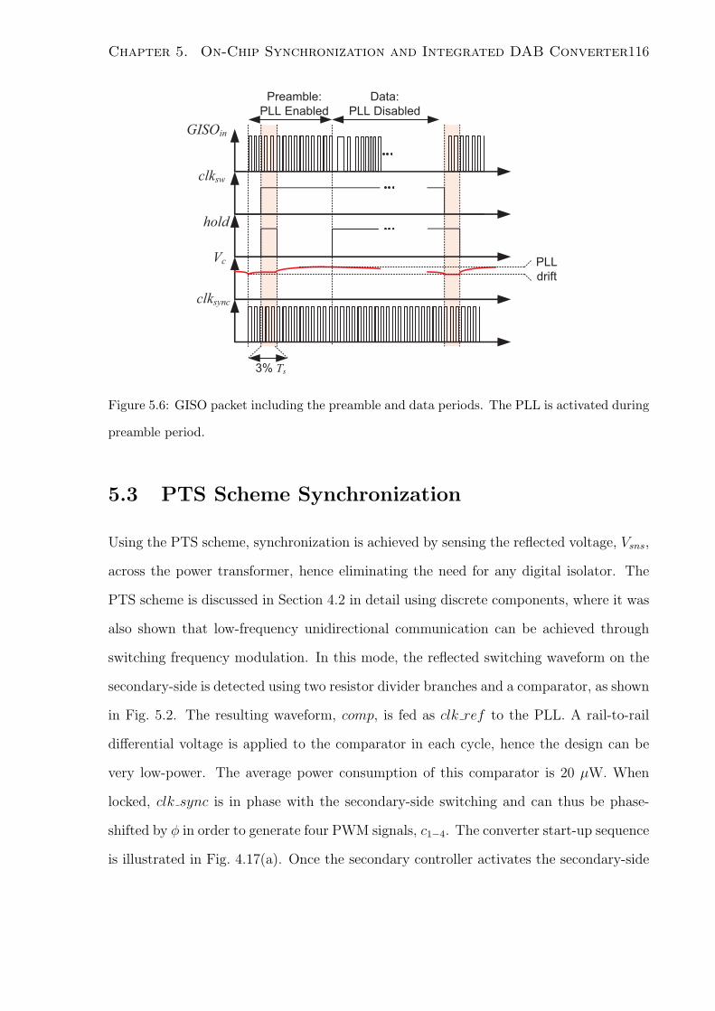
Chapter 5. On-Chip Synchronization and Integrated DAB Converter116
hold
Vc
clksync
GISOin
clksw
Preamble:
PLL Enabled
Data:
PLL Disabled
3% Ts
PLL
drift
Figure 5.6: GISO packet including the preamble and data periods. The PLL is activated during
preamble period.
5.3 PTS Scheme Synchronization
Using the PTS scheme, synchronization is achieved by sensing the reflected voltage, Vsns,
across the power transformer, hence eliminating the need for any digital isolator. The
PTS scheme is discussed in Section 4.2 in detail using discrete components, where it was
also shown that low-frequency unidirectional communication can be achieved through
switching frequency modulation. In this mode, the reflected switching waveform on the
secondary-side is detected using two resistor divider branches and a comparator, as shown
in Fig. 5.2. The resulting waveform, comp, is fed as clk ref to the PLL. A rail-to-rail
differential voltage is applied to the comparator in each cycle, hence the design can be
very low-power. The average power consumption of this comparator is 20 µW. When
locked, clk sync is in phase with the secondary-side switching and can thus be phase-
shifted by ϕ in order to generate four PWM signals, c1−4. The converter start-up sequence
is illustrated in Fig. 4.17(a). Once the secondary controller activates the secondary-side

Chapter 5. On-Chip Synchronization and Integrated DAB Converter117
bridge, the switching is sensed on the primary-side and the PLL is enabled. The charge-
pump output voltage, Vc, is regulated in order to synchronize clk sync to clk ref . Once
PLL locking is achieved, the converter can start-up by driving c1−4.
5.4 Integrated Power Stage
The complete power-stage for a full-bridge topology, shown in Fig. 5.1, consisting of two
low-side and two high-side 80V NDMOS devices is implemented on-chip, as depicted in
Fig. 5.7. Each device has a dimension of 1150 µm × 1080 µm, and is designed to have a
nominal on-resistance, Ron = 100 mΩ at Vgs = 5 V and temperature, Temp = 25C. The
simulated gate-charge of each device, Qg, is 2.2 nC. The final extracted simulation gives
an Ron of 173 mΩ under these conditions and normal process corner. Ron is measured
to be 195 mΩ. Full integration of the primary or secondary-side of the DAB converter
can be achieved using these devices. However, in a two-stage MIV architecture with high
voltage DC-link, discrete high-voltage devices need to be used for the secondary-side.
Four identical gate drivers, each consisting of four inverting stages, are designed to
drive the power FETs. The gate-driver circuit is shown in Fig. 5.8. Two 5V NAND and
NOR logic gates are used to prevent the shoot-through current in the last stage of the
driver. This helps the efficiency and reduces EMI and latch-up issues. Each gate-driver
consumes 26 mW at drive voltage, Vdd5 = 5 V and switching frequency, fs = 1 MHz.
The high-side gate-drivers are supplied by the external bootstrap circuit consisting of an
external capacitor, Cbt, and bootstrap diode, Dbt. High-side and low-side level shifters
are implemented as input stages to the gate-drivers. The design of the high-side level-
shifter is specifically challenging, as high-voltage devices are needed in order to clamp the
voltage on low-voltage driving devices. Furthermore, the level-shifter has to demonstrate
low delay and slew. A stacked topology, with 5V latching pairs, and proposed in [3], is
adopted for this work. The circuit topology is shown in Fig. 5.9(a). FETsMls5−8, are 80V

Chapter 5. On-Chip Synchronization and Integrated DAB Converter118
Vin
+
-
+
-
Vdd
Vdd5
Vdd5
Mh
Ml
Ibias Ibias Vclamp1
Vclamp2
OCP
HS Level-
Shifter
LS Level-
Shifter
Vdd5Vdd
Deadtime
Vx
clkin
Cbt
1 1Ks
DbtVboot
LS
HS
HS_L
LS_L
+
-
+
-
VdVV ddd
VdVV ddd 5dd
MhMM
MlMM
IIbII iasaa IIIbII iasaa VcVV lall mpm 1
VcVV lall mpm 2
OCPCC
HS Level-
Shiftff er
LS Level-
Shiftff er
VdVV ddd 5ddVdVV ddd
Deadtime
VxVV
clkll ik n
1 1KsKK
LS
HSHH
HSHH _L
LS_LMSFp MSFn
Mcl1
Mcl2
Vdd
Vdd
Vdd5 Vdd5
Vdd5Vdd
On-Chip
Over-Current
Protection
HBGND
Bootstrap
Circuit
(a)
LDABVx 1:n
Vx
Vin
Vin
GND
GND
OCP
OCP
Over-Temperature
Protection
OTP
Blanking
clkin
clkin
clks
clks
+
Vx2
-
VxVV
VxVV
ViVV n
ViVV n
GND
GND
OCPCC
OCPCC
Over-Temperature
Protection
OTPTT
Blanking
clkll ikk n
clkll ikk n
clkll sk
HBA
HBB
On-Chip
Vboot
Vboot
V1
V2
Bootstrap
Circuit A
Bootstrap
Circuit B
Vin (<80 V)Vdd5Vdd
Cin
(b)
Figure 5.7: (a) The on-chip half-bridge with over-current protection, and (b) the full primary-
side power-stage of the DAB converter.

Chapter 5. On-Chip Synchronization and Integrated DAB Converter119
Vgate
Mh/Ml
Vx/gnd
Vboot/Vdd5Vin/Vx
HS_L/LS_L
Figure 5.8: The schematic of the gate-driver circuit.
devices which clamp the voltage on upper floating 5V devices, Mls1−4. The transistors
Mls1−2 and Mls3−4 form a pair of latching inverters with the NDMOS transistors Mls5−6,
respectively. The simulated performance of the level-shifter is shown in Fig. 5.9(b). The
level-shifter’s rising and falling delay-time are typically 10 ns, which is reasonable for fs
= 1 MHz. The level-shifter consumes 105 µW on average for Vin = 70 V, and fs = 1
MHz.
Programmable dead-time blocks are implemented based on unit delay cells, as shown
in Fig. 5.10. Each dead-time value is adjustable with 32 different levels, and can achieve
a maximum of 64 ns in nominal conditions.
Peak and valley over-current protection are implemented using two small 80V FETs
(SenseFETs) in parallel with each low-side device, as shown in Fig. 5.7(a) [4]. Current
protection of low-side devices is sufficient, as in the DAB topology, low-side and a high-
side devices of the opposing legs are turned on and off simultaneously. Two current
sources with values Ibias = 2.2 mA, are driven into SenseFETs MSFp and MSFn. The
positive current limit is reached when the drain voltage of MSFp becomes greater than
the drain voltage of Ml, when Ml is on. Similarly, the negative current limit is reached
when the source voltage of Ml becomes greater than the source voltage of MSFn. The
two 80V clamping devices Mcl1 and Mcl2 protect the low-voltage comparator from high

Chapter 5. On-Chip Synchronization and Integrated DAB Converter120
HS_L
HS
Vboot
VxMls5 Mls6
Mls1 Mls3
Mls7 Mls8
Mls2 Mls4
Vdd
MlMM sll 1 MlMM sll 3
MlMM sll 2 MlMM sll 4
Floating 5V Devices
VxVVMlMM sll 5 MlMM sll 6
MlMM sll 7 MlMM sll 8
VdVV ddd
80V Devices
(a)
3 3.5 4 4.5 5 5.5
0
10
20
30
40
50
60
70
Time (µs)
Vo
lta
ge
(V
)
HS
HS_L
Vx
Vdd5
(b)
Figure 5.9: (a) Schematic, and (b) simulated operating waveforms of the high-side level-shifter
at Vin = 70 V.
1x 2x 4x 8x 16x
1x 2x 4x 8x 16x
LS
HSdeadtime[9:5]
deadtime[4:0]
S0 S0 S0 S0 S0
S0 S0 S0 S0 S0
S1 S1 S1 S1 S1
S1 S1 S1 S1 S1
clk_sw
Figure 5.10: The programmable dead-time block.

Chapter 5. On-Chip Synchronization and Integrated DAB Converter121
voltages at switching node Vx by turning on ≈30 ns after Ml is switched on. The
SenseFET scheme provides an almost lossless method for over-current protection, and is
not prone to temperature gradients and process corner variations. The size ratio of the
main device to each SenseFET, Ks, is 1600, resulting in a limit current, Ilimit = ±3.5 A.
An over-temperature protection block is designed based on an on-chip pnp BJT device,
as shown in Fig. 5.11. The emitter-base voltage, Vbe, of the BJT device has a negative
temperature coefficient of ≈ -2.5 mV/C. The circuit block is tuned to trigger at Vbe =
0.634 V, asserting the output OTP at Temp ≈ 115C.
+
-
Vdd
VA
VA(V)
Temp
(°C)
OTP
115
0.634
125 kΩ
230 kΩ
10 µA
Vdd
Figure 5.11: Schematic of the over-temperature protection block.
5.5 Experimental Results
The fabricated DAB synchronization IC is shown in Fig. 5.12 and measures 2.5×4.5
mm2. The chip was tested with a 50 W discrete DAB converter with the parameters
listed in Table 5.1. The start-up process as well as steady-state operation in the
DIS and PTS modes are shown in Fig. 5.13 and Fig. 5.14, respectively. The PLL is
constantly active in PTS mode, except for when hold is high due to PWM edges. The
PLL is put in the hold state in between the data packets as well in DIS mode. The DAB

Chapter 5. On-Chip Synchronization and Integrated DAB Converter122
Mh2
Ml2
Ml1
Mh1 GISO
Digital
Core
and
SPI
PLL
Comparator
(a)
GISO block
Digital
Core
Comparator
Delay Line
SPI
PLL
2.5 mm
4.5 mm
(b)
Figure 5.12: (a) The layout, and (b) the packaged chip micrograph (2.5×4.5 mm2 in 0.18µm
80V BCD process).
current waveform in Fig. 5.15(a) is captured by activating the persistence mode of the
oscilloscope, proving very low PLL jitter in DAB operation. The delay-line, which is the
most power consuming part of the PLL, consumes 0.846 mW on average when oscillating
at the maximum frequency of 100 MHz. The GISO transmission consumes 27 mW in the
transmitter and 63 µW in the receiver when operating continuously at 100 MHz. The
average power consumption of GISO block in DIS mode can be much lower based on the
frequency of communication.

Chapter 5. On-Chip Synchronization and Integrated DAB Converter123
Table 5.1: DAB Converter Prototype Specifications with External Power Stage
Parameter Value Unit
Switching Frequency, fs 500 kHz
DAB Inductance, LDAB 6.9 µH
Primary-Side Voltage, Vin 30 V
Bus Voltage, Vbus 90 V
Transformer Turns Ratio, n 3.5
Nominal Power, PDAB 50 W
The internal power stage was tested by using it as the primary-side in a DAB converter
with specifications listed in Table 5.2. The four internal switches were driven as the
primary-side, while the secondary-side switches were realized using external devices. The
converter’s power stage is shown in Fig. 5.16. The steady-state switching waveforms
when PDAB = 45 W, are shown in Fig. 5.17. The converter achieves 94% efficiency at
this power level, as shown in Fig. 5.18. At low power levels, ZVS is lost, especially
in the high-voltage secondary-side, which in turn reduces the converter’s efficiency. The
efficiency at low power can be boosted by operating in burst-mode [5,6] or Flyback mode.
The zoomed-in primary-side switching nodes, V1 and V2, are shown in Fig. 5.19. Due
to soft-switching and integrated devices, there is no observable ringing, even at fs = 1
MHz. The rise and fall times are ≈ 23 ns. The transition times are a function of DAB
inductor current, ILDAB. In the soft-switching DAB converter, higher currents discharge
the parasitic switching node capacitances faster, which result in shorter transition times.
The over-temperature protection block is tested by running the converter continuously
while increasing the ambient temperature of the IC using a heat-gun. The converter’s
shut-down due to the over-temperature block is shown in Fig. 5.20(b). The over-current

Chapter 5. On-Chip Synchronization and Integrated DAB Converter124
GISOin
Vc
Pre-Charge
hold
700 mV
920 mV
(a)
DataPreamble
hold
Vc
(b)
Figure 5.13: (a) Start-up, and (b) steady state operation of the synchronization process in the
DIS mode.
limit protection is shown in Fig.5.20(a), where the primary-side switching is shut-down
immediately after an intentional step in Vin is introduced. Due to a digital flaw in
the digital logic synthesis process, the low-side power devices are driven on when over-

Chapter 5. On-Chip Synchronization and Integrated DAB Converter125
Vc
Vx2
clk_sync
700 mV
920 mV
(a)
Vx2
Vc
clk_sync
(b)
Figure 5.14: (a) Start-up, and (b) steady state operation of the synchronization process in the
PTS mode.
temperature or over-current signals are asserted. As a result, unwanted oscillations in
ILDAB occur as long as the secondary-side switching is active.

Chapter 5. On-Chip Synchronization and Integrated DAB Converter126
clk_sync
Vx2
GISOin
Vc
ILDAB
(a)
ILDAB
Vc
Vx1
clk_sync
td td
(b)
Figure 5.15: Synchronized DAB converter waveforms in the (a) DIS mode with continuous
GISOin input clock, and (b) PTS mode (ILDAB: 5A/div).

Chapter 5. On-Chip Synchronization and Integrated DAB Converter127
Table 5.2: DAB Converter Prototype Specifications with Internal Power Stage as Primary-Side
Parameter Value Unit
Switching Frequency, fs 1 MHz
DAB Inductance, LDAB 3.9 µH
Primary-Side Voltage, Vin 30-40 V
Bus Voltage, Vbus 87-115 V
Transformer Turns Ratio, n 3
Nominal Power, PDAB 50 W
Input Capacitance, Cin 60 µF
Bus Capacitance, Cbus 20 µF
On-Resistance of Secondary-Side Switches 450 mΩ
On-Resistance of Primary-Side Switches (Integrated) 193 mΩ
Cin LDAB
DAB Transformer
Secondary-Side
Primary
-Side
IC
Figure 5.16: The power stage of the 1 MHz DAB converter with internal primary-side bridge.
The IC is soldered on a separate board and is placed face down on the main power board.

Chapter 5. On-Chip Synchronization and Integrated DAB Converter128
ILDAB
V4
V1
Figure 5.17: Switching waveforms of the integrated DAB converter at Vin = 40 V, Vbus = 115
V, and PDAB = 45 W (ILDAB = 1 A/div).
−50−45−40−35−30−25−20−15−10 −5 0 5 10 15 20 25 30 35 40 45 5078
80
82
84
86
88
90
92
94
PDAB
(W)
Eff
icie
ncy (
%)
Vin
= 30 V, Vbus
= 87 V
Vin
= 35 V, Vbus
= 100 V
Vin
= 40 V, Vbus
= 115 V
Figure 5.18: The efficiency of the DAB converter with integrated primary-side for different Vin
and Vbus.
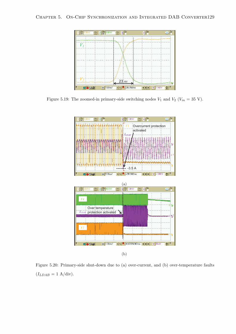
Chapter 5. On-Chip Synchronization and Integrated DAB Converter129
V1
V2 23 ns
Figure 5.19: The zoomed-in primary-side switching nodes V1 and V2 (Vin = 35 V).
V1
ILDAB
-3.5 A
Overcurrent protection
activated
(a)
V1
Over temperature
protection activated
V4
ILDAB
(b)
Figure 5.20: Primary-side shut-down due to (a) over-current, and (b) over-temperature faults
(ILDAB = 1 A/div).
Chapter 5. On-Chip Synchronization and Integrated DAB Converter130
5.6 Chapter Summary
An on-chip demonstration of both PTS, which was first introduced in Chapter 4, and DIS
synchronization schemes are presented in this chapter. While both PLL-based schemes
are superior in cost and performance to the conventional approach of using one opto-
isolator per transistor, they have important differences. A qualitative comparison of
these schemes is provided in Table 5.3. Compared to the DIS scheme, the PLL frequency
in the PTS scheme is limited to the switching frequency, which restricts both the locking
speed and the data transmission rate; however this may be well justified by the reduced
cost and simplicity of operating without any digital isolators. DIS is more expensive and
consumes more power than PTS, since it requires an off-chip air-core transformer for the
GISO transceiver, however it is much more flexible in terms of data communication and
power topology. The DIS scheme can be used in a variety of isolated topologies, while the
PTS scheme’s feasibility needs to be assessed for each specific topology. The developed
IC is promising for future use in high-frequency isolated dc-dc converters.
The power-stage and protection circuits for a full-bridge converter was also imple-
mented. The full-bridge is used as the primary-side of a DAB converter, which achieves
94% peak efficiency at Vin = 40 V and Vbus = 115 V, at PDAB = 45 W. Achieving this
high efficiency is very challenging for silicon devices at 1 MHz switching frequency. While
the power-level is lower than a MIV requirement, which is typically 200-500 W, multiple
integrated primary-side bridges can be used in parallel together with a single high-voltage
secondary-side with discrete devices to realize a much higher power dc-dc stage [7–9].

Chapter 5. On-Chip Synchronization and Integrated DAB Converter131
Table 5.3: Comparison of Driving Schemes in Isolated Converters
Scheme Conventional PTS (Section 5.3) DIS (Section 5.2)
Number of Digital Isolators 4 0 1
Required for Driving (DAB)
Continuous Communication No Yes Optional
(required to avoid PLL drift)
PLL Operation None Low frequency High frequency
Absolute Phase Reference N/A Available through comp Communicated
Communication Capability No Yes Yes
(unidirectional)
Power Consumption High Lowest Low
Power Converter Topology No limitation Limited by No limit
transformer leakage inductance
High Voltage Comparator None Yes No

References
[1] T. Chan Carusone, D. Johns, and K. Martin, Analog Integrated Circuit Design, Second
Ed. Wiley, 2001.
[2] G. Raghul, K. Sudhakar, and M. Devi, “Design and implementation of encoding
techniques for wireless applications,” in International Conference on Circuit, Power
and Computing Technologies (ICCPCT), March 2015, pp. 1–7.
[3] Y. Moghe, T. Lehmann, and T. Piessens, “Nanosecond delay floating high voltage
level shifters in a 0.35 µm hv-cmos technology,” IEEE Journal of Solid-State Circuits,
vol. 46, no. 2, pp. 485–497, Feb 2011.
[4] M. Zaman, Y. Wen, R. Fernandes, B. Buter, T. Doorn, M. Dijkstra, H. Bergveld,
and O. Trescases, “A cell-level differential power processing ic for concentrating-pv
systems with bidirectional hysteretic current-mode control and closed-loop frequency
regulation,” IEEE Transactions on Power Electronics, vol. 30, no. 12, pp. 7230–7244,
Dec 2015.
[5] G. Oggier and M. Ordonez, “High efficiency switching sequence and enhanced dy-
namic regulation for dab converters in solid-state transformers,” in IEEE Applied
Power Electronics Conference and Exposition (APEC), March 2014, pp. 326–333.
[6] A. Rodriguez, A. Vazquez, D. Lamar, M. Hernando, and J. Sebastian, “Different
purpose design strategies and techniques to improve the performance of a dual active
132

REFERENCES 133
bridge with phase-shift control,” IEEE Transactions on Power Electronics, vol. 30,
no. 2, pp. 790–804, Feb 2015.
[7] H. Tao, A. Kotsopoulos, J. Duarte, and M. Hendrix, “A soft-switched three-port
bidirectional converter for fuel cell and supercapacitor applications,” in IEEE Power
Electronics Specialists Conference (PESC), June 2005, pp. 2487–2493.
[8] Z. Wang and H. Li, “An integrated three-port bidirectional dc-dc converter for pv
application on a dc distribution system,” IEEE Transactions on Power Electronics,
vol. 28, no. 10, pp. 4612–4624, Oct 2013.
[9] B. Zhao, Q. Song, W. Liu, and Y. Sun, “Overview of dual-active-bridge isolated
bidirectional dc-dc converter for high-frequency-link power-conversion system,” IEEE
Transactions on Power Electronics, vol. 29, no. 8, pp. 4091–4106, Aug 2014.

Chapter 6
Conclusions
The development of micro and nano-grids based on renewable energy technology is ben-
eficial for the environment, limits the capital cost and eliminates the need for fossil fuel
generators in remote communities and areas with no accessible electrical grid. Stable and
expandable micro and nano-grids should be utilized to satisfy the energy needs of such
areas and communities.
In this work, the important electrical challenges that need to be addressed for the
development of such systems were targeted at various levels. The system-level and archi-
tectural challenges with stability of such systems were discussed in Chapter 2. From a
modularity point of view, a four-quadrant two-stage MIV architecture with active power
smoothing was proposed in Chapter 3. The low-power efficiency and regulation accuracy
of PV inverters are important factors in determining their total energy yield, as solar pan-
els typically spend a significant amount of time generating much lower than their nominal
power. These factors, together with reliability of the proposed MIV architecture, were
improved by introducing the following enhancements to the DAB dc-dc stage in Chapter
4: 1) By slightly modifying the DAB topology, Flyback based operation was achieved,
which has much higher efficiency at low power, and 2) by proposing the PTS scheme, the
need for unreliable digital isolators in this topology was eliminated. The implementation
134

Chapter 6. Conclusions 135
costs can be reduced by lowering the part count of the MIV as well as reducing the size
of passive elements though scaling up the switching frequency. This was addressed by
integrating the full primary-side of the DAB topology, switching synchronization and
phase-shift control modules together on a same IC in Chapter 5.
6.1 Contributions
The main contributions of this dissertation are summarized as follows, in the order in
which they were presented:
1. Nano-Grid Architecture and Control: A fully distributed system-level con-
trol scheme based on droop control was developed. Unlike the conventional droop
scheme for large grids, P -V droop scheme is adopted and applied due to the small
physical size and resistive nature of power cables in the nano-grid. Q-f droop is
also applied for reactive power sharing. The nano-grid voltage is divided into four
operating regions and P -V droop slopes are actively changed for battery invert-
ers in order to eliminate uncontrolled cross-charging and achieving inherent SOC
balancing. The performance of this control scheme is validated by a simulation
test-case, which covers a variety of possible scenarios in a system consisting of mul-
tiple inverters. Furthermore, the stable operation of two paralleled MIVs supplying
a RLC load was demonstrated. The system demonstrates voltage and frequency
transient handling in less than a grid cycle, as well as successful start-up process.
2. MIV Architecture and Control: A four-quadrant MIV architecture which can
interface to PV and battery units was developed. The proposed two-stage MIV ar-
chitecture allows for the integration of short-term LIC storage elements, which are
interfaced via the dc-dc stage. Stable MIV operation is achieved by incorporating
a dual-loop control approach in the dc-dc stage: The DAB converter indirectly reg-
ulates the LIC’s current, while MPPT/battery power regulation is achieved by the

Chapter 6. Conclusions 136
LIC dc-dc converter. The stable operation of this scheme was demonstrated exper-
imentally. The four-quadrant 100 W dc-ac stage operates in BCM current control
and achieves a peak efficiency of 96.3%. A lag-free averaging scheme was presented
and demonstrated on a PV inverter. The real power variations are decreased,
which leads to fuel cost saving, generator lifetime improvement and reduction in
maintenance costs, if a generator is used as a back-up to the nano-grid.
3. DAB Converter Efficiency Enhancement at Low Power: The DAB converter
is employed in the dc-dc stage of the proposed two-stage MIV as the interface be-
tween PV/battery and the bus capacitance. A modification of the DAB converter
in the dual-stage MIV architecture was presented in order to achieve higher effi-
ciency at low power levels. The modified flyback based switching scheme exhibits
higher efficiency than DAB mode at low power levels, which comes at the cost of
an additional switch. The switching losses are significantly reduced by eliminating
most of the switching actions and decreasing the switching frequency. In addition,
it was shown that the Flyback mode achieves higher accuracy in power regulation
for low power levels compared to the DAB mode.
4. Reduction of Digital Isolators for DAB Synchronization: Two switching
synchronization schemes, PTS and DIS, were developed for the isolated topologies
in order to eliminate the need for expensive and unreliable digital isolators. The DIS
scheme only requires one digital isolator as the switching information are modulated
by a high-frequency carrier and transmitted over the converter’s isolation boundary,
while the PLL-based PTS scheme does not require any digital isolators and is based
on sensing the reflected voltage on the power transformer’s taps. The PTS scheme
was demonstrated on a DAB prototype. Low-frequency communication based on
this scheme was also demonstrated with minimal additional complexity. A proposed
dual-comparator approach successfully mitigates the inherent issue of PTS scheme

Chapter 6. Conclusions 137
for the DAB converter with high leakage inductance. It was shown that PTS scheme
can be potentially adapted to work for other isolated topologies as well.
5. Integrated DAB Converter: An on-chip demonstration of both PTS and DIS
synchronization schemes for the DAB converter were presented in a 0.18µm 80V
process. For this purpose, an integrated on-chip PLL is implemented, which can
lock to a wide frequency range, 500 kHz-100 MHz. In addition, precise phase-shift
is achieved with a resolution of 300 ps in order to control the power-flow. For DIS
mode, a low-power GISO transceiver is implemented on-chip, which can transmit
and receive bitstreams of up to 100 MHz using a small off-chip air-core transformer.
As CMOS technology node continues to shrink for digital applications, there is also
a strong interest of integrating high-voltage devices in standard low-voltage CMOS
process for high-voltage applications. As a result, a complete power-stage for a
full-bridge converter is implemented on-chip as well.
The performance of PTS and DIS schemes were demonstrated using an off-chip
DAB converter, while efficient operation of the internal power stage was demon-
strated separately. The integrated power converter achieves 94% efficiency at 45
W.
6.2 Future Work
The following topics are recommended extensions of the work presented in this disserta-
tion:
1. System-Level Planning and Control: Load shedding is necessary when gen-
eration and storage elements’ SOC levels are insufficient to meet the momentary
load demands. However, loads can be shed due to a specific energy management
policy which is programmed into the IDP. Lower priority loads can be shed during
peak hours of generation in order to save more energy for night hours, when more

Chapter 6. Conclusions 138
important loads need to be powered. In addition, the effect of deep discharge and
increased charge/discharge cycles on the lifetime of the batteries should be taken
into account. Very high-level system simulations with a focus on real power-flow
should be set up in order to investigate various load shedding and energy planning
strategies. Typical household load profile, generation predictive models, and bat-
tery storage models need to be constructed and used in this simulation test bed.
The results will be used in developing effective policies for load and generation
management, leading to a smart nano-grid system.
2. System-Level Stability Analysis and Parameter Optimization: The droop-
based system-level control scheme presented in Chapter 2 can be further studied
analytically to optimize the parameters and ensure the frequency and voltage sta-
bility over the wide operating range of the nano-grid, while considering the device
limits. The stability analysis problem proves to be quite challenging due to the AC
operation and multiple MIVs working in parallel; however there have been efforts
to address such systems from the control perspective. The derivation of a full ana-
lytical model will also be useful for high-level control in order to adaptively adjust
the droop parameters based on the nano-grid’s status. This will result in a higher
quality power delivery and improved transient behavior.
3. Extension of PTS Scheme to Other Isolated Topologies: The PTS scheme
works based on using the power transformer as a communication means across the
isolation boundary. This scheme can be extended to other isolated topologies; how-
ever, its effective operation is dependant on the switching information that can be
derived from sensing the reflected voltage on the transformer’s taps. The successful
adaptation of PTS scheme to other isolated topologies can save implementation
costs by reducing the number of digital isolators needed for data communication
as well as transmitting gating signals over the isolation boundary in order to drive

Chapter 6. Conclusions 139
active switches.

Appendix A
Intelligent Distribution Panel
The nano-grid is configured as a collection of autonomous PV and battery inverters
connected to loads via an IDP. The IDP is at the core of the nano-grid, and serves to
monitor solar generation, storage levels, and loads. It can also provide high-level control
for droop slope adjustments and load shedding policy. IDPs can be connected together
to form an autonomous, interconnected network where energy-deprived IDPs seek access
to energy sources through neighboring IDPs.
While the primary objective of this dissertation is to address problems associated
with rural electrification, this concept can also benefit urban installations. The IDP’s
ability to shed loads enhances grid stability and reduces consumers’ utility costs by saving
energy during peak billing periods.
A.1 IDP Architecture
An IDP is developed completely in-house based on a typical residential electrical distri-
bution panel which is augmented with the following components:
1. A DC Uninterruptible Power Supply (UPS).
2. Modular smart breakers and metering hardware.
140

Appendix A. Intelligent Distribution Panel 141
3. Communication bus.
4. Motherboard hosting the central controller unit.
The IDP architecture and main components are shown in Fig. A.1.
V
L
N
Filter
ADC Voltage
ConditioningPeak
detector
Relay Driver
Filter
M
U
X
10
4-bit
address
Power Board
DAQ Board
V
L
N
Filter
ADC Voltage
ConditioninggPeak
detector
Relay Driver
Filter
M
U
X
4-bit
address
Power Board
DAQ Board
Channel 1
UPS
MCU
(BeagleBone
Black)
USB
UART PC
DC-DC Voltage
RegulatorsUPS
MCU
(BeagleBone
Black))
USB
UART
DC-DC Voltage
ReggulatorsMotherboard
Filter ADC
V
DPST Relay
V
L
N
Filter
ADC Voltage
ConditioningPeak
detector
Relay Driver
Filter
M
U
X
5 V24 V
Power Board
DAQ Board
V
L
N
Filter
ADC Voltage
ConditioninggPeak
detector
Relay Driver
Filter
M
U
X
5 V24 V
Power Board
DAQ Board
Channel n
V
DPST Relay
Voltage sensing
4-bit
address
24-V DC Output
24-V DC
Output AC Input
5 V24 V
ComminucationandAux.PowerBus
Figure A.1: IDP Architecture.
The smart breakers are responsible for monitoring and controlling the status of each
AC channel. A smart breaker can be broken into two core components, a Data Acquisition
(DAQ) board and a power board, which are assembled together, as shown in Fig. A.2.
The power board monitors and controls the AC current flow in each channel. It is
equipped with a voltage detector circuit to sense the presence of AC voltage, as well as two

Appendix A. Intelligent Distribution Panel 142
Hall sensors, which measure the current flowing through the breaker. The power board
also houses a Double Pole Single Throw (DPST) relay that opens/closes the channel
based on the command from the central controller.
The main role of the DAQ board is to process and translate the analog information
from the power board into digital signals and drive the relay on the power board. All
analog signals are fed to an anti-aliasing second-order Sallen-Key filter [1]. The filter’s
output is sampled by an Analog-to-Digital Converter (ADC) at 12.5 kSample/sec. The
digital data is transmitted to the central controller through the Serial Peripheral Interface
(SPI) line on the communication bus. The same SPI line is also used by the central
controller to send commands to the 24-V relay driver on the DAQ board. When activated,
the relay disconnects the AC line at the zero-crossings of the electrical current.
Relay
Hall-Effect
Current Sensors
Power Board
DAQ Board
Figure A.2: Assembled Power and DAQ boards.
The motherboard, as shown in Fig. A.3, houses the central processor unit and provides
connections to all peripherals including the smart breakers and the 240/120-VAC to 24-V
DC UPS. The UPS is only meant to power the internal circuitry of IDP during a power
outage. This unit is equipped with a battery sized to maintain the IDP operation for
twelve hours without grid power.
An additional feature of the motherboard is nano-grid voltage sensing. The voltage
sensing network is similar to the current sensing circuitry on the smart breakers. A

Appendix A. Intelligent Distribution Panel 143
high-precision voltage divider generates an analog signal that is passed through an anti-
aliasing Sallen-Key filter before it is fed to a 12-bit ADC. The sampled voltage is then
transmitted via an opto-coupler to the CPU.
The information collected on individual channels are routed to a central processing
unit on the IDP, the Beaglebone Black (BBB). The BBB utilizes a Cortex A8 CPU
clocked at 1 GHz, suitable for real-time complex power measurement and supervisory
control algorithms. Additionally, wireless adaptors can be added through available pe-
ripheral USB ports.
BeagleBone BlackVoltage
Regulator
Voltage
RegulatorVoltage
Sensor
Figure A.3: The IDP motherboard PCB (top view).
A.2 Measurements and Processing
The voltage and current harmonic contents, which are mainly caused by non-linear loads,
are an important reason for reduced power quality and device break-downs [2]. Excess
harmonic contents induce excessive losses and can lead to failures of electrical equipment
and appliances. They must be closely monitored and mitigated in power infrastructure.
In areas where a stiff grid is not available, particularly in the case of the nano-grid,
monitoring harmonics is challenging since the fundamental frequency is subject to higher
volatility due to lack of mechanical inertia in the system. The varying grid frequency and
harmonic contents render the computationally intensive Fast Fourier Transform (FFT)
based algorithms ineffective [3, 4].

Appendix A. Intelligent Distribution Panel 144
In order to achieve efficient low-latency power and frequency measurements, a Mul-
tiple Second Order General Integrator - Frequency-Locked-Loop (MSOGI-FLL) [3, 4] is
implemented in the IDP to monitor the fundamental, harmonics, and frequency of the
AC voltage and individual channel AC currents. The simplified schematic of a Second
Order General Integrator (SOGI) with FLL is shown in Fig. A.4. The MSOGI-FLL
utilizes multiple second order bandpass filters, formed using integrators, in combination
with a frequency locked loop to lock to the fundamental component and its harmonics.
The MSOGI-FLL code was developed and simulated in MATLAB to verify its pre-
cision in tracking the fundamental, harmonics and line frequency, f . The trajectory of
MSOGI-FLL tracking a specific function, u(t), is illustrated in Fig. A.5. u(t) is defined
as
u(t) = 10 · cos(2πft) + 5 · cos(2π(3f)t) + (A.1)
2 · cos(2π(7f)t),
where f = 55 Hz, which is the highest/lowest allowable operational value for the nano-
grid frequency based on the Q-f droop characteristic, when fnom = 50/60 Hz.
+
-k +
-ò
ò
ò
u(t)u’(t)
f’
qv’
-k’
ò-k’
+-
ò
òqv’
FLL
SOGI
Figure A.4: SOGI-FLL architecture [3].
High-level control can be implemented in the IDP processing platform. At start-up,
the nano-grid’s voltage is checked to ensure it is in a stable state for loads to connect.
With the grid stabilized and all the loads connected, the IDP continuously calculates the

Appendix A. Intelligent Distribution Panel 145
0 0.1 0.2 0.3 0.4 0.5 0.644
46
48
50
52
54
56
Time (s)
F (
Hz)
(a)
0 0.1 0.2 0.3 0.4
−10
−5
0
5
10
Time (s)
Amplitude
Fundamental
3rd Harmonic
5th Harmonic
7th Harmonic
(b)
Figure A.5: Simulation results for MSOGI-FLL demonstrating the start-up and successful
locking to the (a) frequency, and (b) fundamental and harmonics contents of u(t).
power flowing through each smart breaker on a regular basis. The power measurements
and diagnostic results are transmitted to a user-designated device (local computer, smart
phone, etc.) through the BBB USB port. Should any of the channels draw power
exceeding the pre-defined limits, the IDP automatically disconnects the relevant relay
and alerts the user. In a grid-tied system, users can also program the IDP to disconnect
low priority loads during periods of peak billing to save up on their electricity bills in
case a grid-tied system is in use.
When faults or power shortage occur, each IDP can help restore the grid by shedding
loads based on their power ratings and user-designated priority. In addition, it is possible
to connect two IDPs through one of the channels and allow power to flow from one IDP
to another at users’ discretion.
A.3 IDP Experimental Results
The assembled IDP is shown in Fig. A.6. The dimensions of power and DAQ boards are
such that they are compatible with existing AC panels. The measurement results of IDP
versus the e-load reading at four different load profiles and varying frequency are detailed

Appendix A. Intelligent Distribution Panel 146
Power and
DAQ boards
Mo
the
rbo
ard
UP
S a
nd
Battery
Communication Bus
Communication Bus
Figure A.6: Assembled ten-channel IDP.
Line Current
Smart Break ON
Command
Hard turn-on
(a)
Line Current
Smart Break OFF
Command
Soft turn-off
(b)
Figure A.7: The smart breaker command and AC line current when (a) connecting, and (b)
disconnecting the channel.
in Table A.1. The results match within 1% at high power levels (≥ 100 W/VAR/VA),
while at low power, significant inaccuracy can occur. This is due to the offset errors of
the measurement devices, and can be reduced by calibrating these devices.
The relay turn-on and turn-off events are shown in Fig. A.7 (a), (b), respectively.
The relay disconnect happens at AC current’s zero crossing, and it is envisioned that the
turn-on can also benefit from soft switching by proper timing control.

Appendix A. Intelligent Distribution Panel 147
Table A.1: Comparison of IDP MSOGI-FLL Outputs and Readings from E-Load for Four Test
Cases
Test 1 P (W) Q (VAR) S (VA) f (Hz)
E-load Reading 694.10 620.00 930.52 59.99
IDP Measurement 687.31 624.54 928.69 60.08
Error Percentage -0.98 % 0.76 % -0.20 % 0.15 %
Test 2 P (W) Q (VAR) S (VA) f (Hz)
E-Load Reading 12.6 4.23 13.27 59.99
IDP Measurement 12.79 3.06 13.16 60.09
Error Percentage -1.5 % 1.50 % -0.82 % 0.16 %
Test 3 P (W) Q (VAR) S (VA) f (Hz)
E-Load Reading 91.05 657.57 664.19 59.99
IDP Measurement 72.41 653.48 657.48 60.07
Error Percentage -20.47 % -0.62 % -1.01 % 0.13 %
Test 4 P (W) Q (VAR) S (VA) f (Hz)
E-Load Reading 811.71 830.74 1161.66 55.01
IDP Measurement 804.24 833.32 1158.11 55.47
Error Percentage -0.92 % 0.31 % -0.30 % 0.85 %

Appendix A. Intelligent Distribution Panel 148
A.4 Appendix Summary
An intelligent power distribution panel that can monitor and control power-flow in a
nano-grid was presented in this appendix. The IDP can enhance grid stability by pro-
viding a platform for monitoring, processing and high-level control. The IDP concept
can be extended to grid-tied systems, where it can be used to reduce utility costs and
enhance grid stability. Experimental and simulation results demonstrate that the IDP
can accurately track the real and reactive power, grid frequency, and fundamental and
harmonic contents under various loads and grid conditions. It can also individually con-
trol different channels through built-in relays. This feature is necessary for load shedding,
generation and storage management.

References
[1] D. Jurisic, G. S. Moschytz, and N. Mijat, “Low-sensitivity active-RC high- and band-
pass second-order Sallen Key allpole filters,” in IEEE International Symposium on
Circuits and Systems (ISCAS), vol. 4, 2002, pp. IV–241–IV–244 vol.4.
[2] J. Desmet, C. Debruyne, J. Vanalme, and L. Vandevelde, “Power injection by dis-
tributed generation and the influence of harmonic load conditions,” in 2010 IEEE
Power and Energy Society General Meeting, July 2010, pp. 1–6.
[3] P. Rodriguez, A. Luna, I. Candela, R. Mujal, R. Teodorescu, and F. Blaabjerg, “Mul-
tiresonant frequency-locked loop for grid synchronization of power converters under
distorted grid conditions,” IEEE Transactions on Industrial Electronics, vol. 58, no. 1,
pp. 127–138, Jan 2011.
[4] J. Matas, M. Castilla, J. Miret, L. Garcia de Vicuna, and R. Guzman, “An adap-
tive prefiltering method to improve the speed/accuracy tradeoff of voltage sequence
detection methods under adverse grid conditions,” IEEE Transactions on Industrial
Electronics, vol. 61, no. 5, pp. 2139–2151, May 2014.
149

Appendix B
Household Load Modeling and
Emulation
Typical household load profiles have to be captured and emulated in the target nano-
grid demo, as depicted in Fig. 1.6. A semi-automated process is developed in order to
perform this task for given single-phase AC electrical appliances. This process consists
of two main phases:
1. Acquisition, which includes measuring and saving the load’s AC current as well as
the grid voltage.
2. Analysis and emulation, which includes breaking down the AC voltage and current
data into certain meaningful variables, and using this information to aggregate and
emulate the load profiles using an e-load.
This appendix addresses these two main phases in the following two sections.
B.1 Load Profile Acquisition
An isolated voltage probe together with a current probe are used to capture and save
the data on a portable oscilloscope. Using a digital oscilloscope is advantageous to data-
150

Appendix B. Household Load Modeling and Emulation 151
loggers as it includes high-speed ADCs, as well as real-time flexibility to set the timescale,
and capture the load transient and start-up profiles. The load acquisition setup diagram is
shown in Fig. B.1(a). An AC double-socket power outlet receptacle, shown in Fig. B.1(b),
is transformed to easily connect to the isolated voltage probe through the second socket,
and provide the current loop for the hall-sensor based current probe.
Load Under Test
Isolated
Voltage
Probe
Current
Probe
Portable
Digital
Oscilloscope
Hard
Drive
AC Grid
L
N
ig(t)
+
vg(t)
-
CH1
CH2
(a)
On/Off
Switch
Current
Loop
Socket 1
Socket 2
(b)
Figure B.1: (a) The load acquisition setup diagram, and (b) the modified double-socket power
outlet receptacle.
The load characterization has been done for more than 20 different common loads,
such as oven, air conditioning unit, and wall charger, in a typical North American house-
hold. Captured steady-state voltage and current waveforms for a small fan and microwave
are shown in Fig. B.2(a), (b), respectively.
B.2 Load Profile Emulation
The load profile can be emulated using an e-load. A 3.6 kW Chroma 63803 AC e-load
is used for this purpose [1]. The emulation is done through setting up a combination of
crest and power factors, CF and PF , through the e-load. A true four quadrant e-load
can accurately model the characterized load profile, however, to the best of the author’s

Appendix B. Household Load Modeling and Emulation 152
0.24 0.26 0.28 0.3 0.32 0.34 0.36−8
−6
−4
−2
0
2
4
6
8
Time (s)
Vg (
V)
an
d I
g (
A)
Voltage
Current
(a)
1.82 1.84 1.86 1.88 1.9 1.92 1.94−25
−20
−15
−10
−5
0
5
10
15
20
Time (s)
Vg (
V)
and I
g (
A)
Voltage
Current
(b)
Figure B.2: Grid voltage and steady-state AC current of a typical (a) small fan, and (b)
microwave (Vg attenuated by 100×).

Appendix B. Household Load Modeling and Emulation 153
vg(t)MSOGI-
FLL T><2()
fT
1=
T><2()
ig(t)
T><()
PF
P
S
Peak
Detector Ig,peak
Ig
Vg
CF
PLTo the
e-load
Figure B.3: The load characterization process.
knowledge, all the off-the-shelf AC e-loads in the market utilize a diode rectifier stage,
succeeded by a RLC passive filter bank. The load characterization process is shown in
Fig. B.3. The captured voltage waveform is passed to a MSOGI-FLL block, which is
described in Chapter 2, and the fundamental frequency, f , is determined. The active
and reactive power as well as the PF are deduced consequently. The CF is determined
as Ig,peak/Ig, where Ig,peak is the peak of the current waveform. These values, together
with the desired real load power, PL, are transmitted to the e-load through the serial
RS-232 port. In case multiple loads need to be aggregated and emulated by the e-load,
the reconstructed waveforms are added together, and the process is repeated for the
aggregated sum. The AC current of a commercial phone charger, and the reconstructed
waveform by the e-load are shown in Fig. B.4 (a), (b), respectively.

Appendix B. Household Load Modeling and Emulation 154
(a)
0.15 0.16 0.17 0.18 0.19 0.2 0.21 0.22 0.23 0.24
−0.1
−0.05
0
0.05
0.1
−0.1
−0.05
0
0.05
0.1
−0.1
Time (s)
AC
Cu
rre
nt
(A)
(b)
Figure B.4: (a) The AC current measurement, and (b) the reconstructed waveform for a typical
60 W laptop charger in idle state (not charging).

Appendix B. Household Load Modeling and Emulation 155
B.3 Appendix Summary
In this chapter, a semi-automated process was developed in order to aggregate and emu-
late the AC load profile for typical household appliances using an e-load. The acquisition
is performed by a setup consisting of a digital oscilloscope, and current and voltage
probes, while the analysis is performed using custom developed software in MATLAB.
Extracted PF and CF are then used to reconstruct the current waveform. These two
steps were demonstrated on a 60 W laptop charger in idle state.

References
[1] “Programmable ac and dc electronic load model 63800 series,” Chroma, available
http://www.chromausa.com/pdf/63800-E.pdf.
156