c 2005 by peter jeremy czoschke. all rights reserved
TRANSCRIPT

c© 2005 by Peter Jeremy Czoschke. All rights reserved.

QUANTUM ELECTRONIC EFFECTS IN ULTRATHIN METALFILMS ON SEMICONDUCTORS
BY
PETER JEREMY CZOSCHKE
B.A., Carleton College, 1997M.S., University of Illinois at Urbana-Champaign, 2002
DISSERTATION
Submitted in partial fulfillment of the requirementsfor the degree of Doctor of Philosophy in Physics
in the Graduate College of theUniversity of Illinois at Urbana-Champaign, 2005
Urbana, Illinois
Abstract
As the size of a metallic system approaches the atomic scale, deviationsfrom the bulk are expected in a plethora of different physical properties dueto quantum size effects. In this work, two of these effects are investigatedin detail: the structural distortions that arise due to quantum confinementof a metal’s itinerant electrons to an ultrathin film and variations in thesurface energy (relative stability) of such films as a function of thickness.These effects are first examined from a theoretical viewpoint, where modelsbased upon a free-electron gas confined to a one-dimensional quantum wellare derived to illustrate the basic physical phenomena. These models areengineered such that they are realistic enough to be used in the analysis ofempirical data with the adjustment of a small number of phenomenologicalparameters.
These effects are then investigated experimentally using surface x-raydiffraction at a third-generation synchrotron radiation facility (the AdvancedPhoton Source at Argonne National Laboratory). Extended reflectivityspectra from smooth atomic-scale Pb films prepared on Si(111) substratesat 110 K are obtained for thicknesses of 6–19 atomic layers that exhibitdistinctive features indicative of quasibilayer lattice distortions. A detailedanalysis shows variations within the layer structure of each film that are cor-related with Friedel-like charge density oscillations at the film boundaries.Variations in the lattice distortions are also observed as a function of thick-ness with a quasibilayer periodicity. This effect is explained in the contextof quantum size effects using the theoretical models.
A second experiment is also described in which initially smooth Pb filmsare progressively annealed from 110 K to near room temperature. The filmmorphology is examined every 5–10 K by scanning the extended x-ray re-flectivity, which reveals the initially smooth films breaking up into islandsof specific heights. Once the samples reach a state of quasi-equilibrium,the distributions of island heights are measured, which show strong quasi-bilayer variations in the relative stability of different height islands (filmthicknesses). These variations are related to electronic contributions to thesurface energy using the free-electron-based theoretical models.
iii

Acknowledgments
This research and dissertation would not have been possible without thehelp and support of many people. In particular, I would like to thank myadvisor, Professor Tai-Chang Chiang, for always being there for questions,answers, or just friendly discussions. I would also like to thank the staffat the UNICAT beamline, in particular Hawoong Hong, who spent many alate night with me troubleshooting a technical problem or mulling over thelatest strange diffraction pattern we were seeing. Past and current membersof the Chiang National Lab research group also deserve mention, especiallyTim Kidd and Martin Holt, who both helped me in those early years ofmy graduate career when I needed to learn the basics and develop the self-confidence to be a good scientist.
I am also very grateful for the personal support I received from myfamily. Many thanks go to my Mom and Dad, who instilled in me a greatlove for learning and a thirst for knowledge; to my wife, Becky, who waswilling to pull up anchor in Minnesota from her friends and family to comeout to the middle of corn country, just to let me follow my dream of gettingthe best education possible. Her love and support were always there for me,something on which I knew I could always rely. Last but not least, a bigkiss and hug go to my baby daughter, Meredith, who showed (is showing)me what the truly important things in life are.
This work is based upon work supported by the U.S. Department of En-ergy, Division of Materials Sciences (Grant No. DEFG02-91ER45439). TheUNICAT facility at the Advanced Photon Source (APS) is supported bythe U.S. Department of Energy through the Frederick Seitz Materials Re-search Laboratory at the University of Illinois at Urbana-Champaign, theOak Ridge National Laboratory, the National Institute of Standards andTechnology, and UOP LLC. The APS is supported by the U.S. Departmentof Energy (Grant No. W-31-109-ENG-38). We also acknowledge partialequipment and personnel support from the Petroleum Research Fund, ad-ministered by the American Chemical Society, and the U.S. National ScienceFoundation (Grant No. DMR-02-03003).
iv

Table of Contents
Page
List of Figures . . . . . . . . . . . . . . . . . . . . . . . . . . . . vii
List of Tables . . . . . . . . . . . . . . . . . . . . . . . . . . . . ix
List of Abbreviations . . . . . . . . . . . . . . . . . . . . . . . x
List of Symbols and Constants . . . . . . . . . . . . . . . . . . xi
1 Introduction . . . . . . . . . . . . . . . . . . . . . . . . . . . 11.1 Quantum Size Effects . . . . . . . . . . . . . . . . . . . . . . 11.2 Step Height Oscillations in Ultrathin Metal Films . . . . . . . 21.3 The Preferred or “Magic” Thickness Effect . . . . . . . . . . 4
2 Surface X-Ray Diffraction . . . . . . . . . . . . . . . . . . . 72.1 Introduction . . . . . . . . . . . . . . . . . . . . . . . . . . . . 72.2 Crystal Lattices . . . . . . . . . . . . . . . . . . . . . . . . . . 8
2.2.1 The Unit Cell . . . . . . . . . . . . . . . . . . . . . . . 82.2.2 Miller Indices and Crystal Planes . . . . . . . . . . . . 102.2.3 Surface Coordinates . . . . . . . . . . . . . . . . . . . 13
2.3 Diffraction and the Reciprocal Lattice . . . . . . . . . . . . . 142.3.1 Bragg Reflections . . . . . . . . . . . . . . . . . . . . . 142.3.2 The von Laue Formalism . . . . . . . . . . . . . . . . 16
2.4 Reconstructions and Superperiodicities . . . . . . . . . . . . . 192.5 Calculation of the Scattered Intensity . . . . . . . . . . . . . 21
2.5.1 The Structure Factor . . . . . . . . . . . . . . . . . . . 212.5.2 Diffraction from a 3D Crystal . . . . . . . . . . . . . . 262.5.3 Diffraction from a Film . . . . . . . . . . . . . . . . . 282.5.4 Geometrical Correction Factors . . . . . . . . . . . . . 30
2.6 Extended Reflectivity of a Pb/Si(111) Film . . . . . . . . . . 352.6.1 Overview . . . . . . . . . . . . . . . . . . . . . . . . . 352.6.2 Substrate Amplitude Contribution . . . . . . . . . . . 362.6.3 Film Structure Factor . . . . . . . . . . . . . . . . . . 372.6.4 Calculation of the Measured Intensity . . . . . . . . . 39
3 Experimental Methods . . . . . . . . . . . . . . . . . . . . . 433.1 Introduction . . . . . . . . . . . . . . . . . . . . . . . . . . . . 433.2 Ultrahigh Vacuum . . . . . . . . . . . . . . . . . . . . . . . . 44
3.2.1 Characteristics . . . . . . . . . . . . . . . . . . . . . . 443.2.2 Vacuum Pumps . . . . . . . . . . . . . . . . . . . . . . 46
v

3.2.3 Achieving UHV . . . . . . . . . . . . . . . . . . . . . . 483.3 X-Ray Detectors . . . . . . . . . . . . . . . . . . . . . . . . . 50
3.3.1 Point Detectors . . . . . . . . . . . . . . . . . . . . . . 503.3.2 Measurement Corrections . . . . . . . . . . . . . . . . 52
3.4 Experimental Setup . . . . . . . . . . . . . . . . . . . . . . . 563.4.1 The UNICAT Beamline Sector 33ID at the APS . . . 563.4.2 The SXRD Station at Sector 33ID . . . . . . . . . . . 59
3.5 Sample Preparation . . . . . . . . . . . . . . . . . . . . . . . 633.5.1 Molecular Beam Epitaxy . . . . . . . . . . . . . . . . 633.5.2 Sample Pretreatment . . . . . . . . . . . . . . . . . . . 64
3.6 Collection of X-Ray Reflectivity Data . . . . . . . . . . . . . 663.6.1 The Rocking Curve Method . . . . . . . . . . . . . . . 663.6.2 The Ridge Scan Method . . . . . . . . . . . . . . . . . 723.6.3 Error Analysis . . . . . . . . . . . . . . . . . . . . . . 75
4 Free-Electron Models . . . . . . . . . . . . . . . . . . . . . 764.1 Introduction . . . . . . . . . . . . . . . . . . . . . . . . . . . . 764.2 Charge Density . . . . . . . . . . . . . . . . . . . . . . . . . . 774.3 Fermi Level . . . . . . . . . . . . . . . . . . . . . . . . . . . . 814.4 Lattice Distortions . . . . . . . . . . . . . . . . . . . . . . . . 87
4.4.1 Overview . . . . . . . . . . . . . . . . . . . . . . . . . 874.4.2 The Local Charge Density Gradient . . . . . . . . . . 894.4.3 The Electrostatic Force . . . . . . . . . . . . . . . . . 90
4.5 Surface Energy . . . . . . . . . . . . . . . . . . . . . . . . . . 924.5.1 Overview . . . . . . . . . . . . . . . . . . . . . . . . . 924.5.2 Infinite Well . . . . . . . . . . . . . . . . . . . . . . . . 924.5.3 Finite Well . . . . . . . . . . . . . . . . . . . . . . . . 96
5 Lattice Distortions in Pb/Si(111) Films . . . . . . . . . . 1025.1 Experiment Overview . . . . . . . . . . . . . . . . . . . . . . 1025.2 Growth Behavior . . . . . . . . . . . . . . . . . . . . . . . . . 1025.3 Quasibilayer Lattice Distortions . . . . . . . . . . . . . . . . . 1065.4 Discussion and Comparison with Other Studies . . . . . . . . 1125.5 Summary . . . . . . . . . . . . . . . . . . . . . . . . . . . . . 115
6 Surface Energy of Pb/Si(111) Films . . . . . . . . . . . . . 1166.1 Experiment Overview . . . . . . . . . . . . . . . . . . . . . . 1166.2 Extended X-Ray Reflectivity Analysis . . . . . . . . . . . . . 1176.3 Evolution of Film Morphology with Annealing . . . . . . . . 1236.4 Surface Energy . . . . . . . . . . . . . . . . . . . . . . . . . . 1286.5 Discussion . . . . . . . . . . . . . . . . . . . . . . . . . . . . . 1316.6 Summary . . . . . . . . . . . . . . . . . . . . . . . . . . . . . 132
7 Conclusions and Outlook . . . . . . . . . . . . . . . . . . . 133
References . . . . . . . . . . . . . . . . . . . . . . . . . . . . . . 135
Author’s Biography . . . . . . . . . . . . . . . . . . . . . . . . 142
vi

List of Figures
Figure Page
1.1 Microscopy images showing evidence of lattice distortions . . 31.2 Scanning tunneling microscopy image of flat-topped islands
with preferred heights . . . . . . . . . . . . . . . . . . . . . . 51.3 Oscillations in the surface energy found from first-principles
calculations . . . . . . . . . . . . . . . . . . . . . . . . . . . . 6
2.1 The fcc and diamond lattices . . . . . . . . . . . . . . . . . . 92.2 Stacking of the fcc(111) lattice planes . . . . . . . . . . . . . 112.3 (111) atomic planes of the diamond lattice. . . . . . . . . . . 122.4 Unit cell for a fcc(111) surface . . . . . . . . . . . . . . . . . 132.5 Diagram showing the Bragg angle and momentum transfer . . 152.6 Example of a surface reconstruction . . . . . . . . . . . . . . 202.7 Scattering geometry for a single electron . . . . . . . . . . . . 232.8 Atomic scattering factor for Si . . . . . . . . . . . . . . . . . 252.9 N -slit interference function . . . . . . . . . . . . . . . . . . . 282.10 Schematic showing interference between the top layers of a film 372.11 Example reflectivity profiles for Pb/Si(111) films . . . . . . . 40
3.1 Detector dead time effect for a scintillation detector . . . . . 543.2 Aerial view of the APS . . . . . . . . . . . . . . . . . . . . . . 563.3 Diagram of a wiggler or undulator . . . . . . . . . . . . . . . 573.4 Picture of an undulator at the APS . . . . . . . . . . . . . . . 583.5 Schematic of a double-crystal monochromator . . . . . . . . . 593.6 Diffractometer and UHV chamber . . . . . . . . . . . . . . . 603.7 Sample mount . . . . . . . . . . . . . . . . . . . . . . . . . . . 623.8 Raw reflectivity data for different surfaces during sample prepa-
ration . . . . . . . . . . . . . . . . . . . . . . . . . . . . . . . 653.9 Diagram of the scattering geometry slightly offset from the
specular condition . . . . . . . . . . . . . . . . . . . . . . . . 673.10 Comparison of data collected with the rocking curve and ridge
scan methods . . . . . . . . . . . . . . . . . . . . . . . . . . . 683.11 Maps of a Pb/Si(111) reflectivity rod in angular space and
reciprocal space . . . . . . . . . . . . . . . . . . . . . . . . . . 693.12 Diagram showing the range of momentum transfer collected
by the detector slits . . . . . . . . . . . . . . . . . . . . . . . 71
4.1 The Fermi sphere of allowed states in a film . . . . . . . . . . 784.2 The self-normalized charge density variations in a metal film 804.3 Fermi energy of a Pb(111) film . . . . . . . . . . . . . . . . . 83
vii

LIST OF FIGURES
4.4 Charge density profiles for the infinite quantum well model . 844.5 The Fermi energy for a charge balanced Pb(111) film . . . . . 864.6 The charge density and electric field in an infinite quantum
well . . . . . . . . . . . . . . . . . . . . . . . . . . . . . . . . 894.7 Surface energy of a Pb(111) film using the infinite quantum
well model . . . . . . . . . . . . . . . . . . . . . . . . . . . . . 954.8 Schematic of the finite quantum well . . . . . . . . . . . . . . 964.9 Surface energy using the finite quantum well model . . . . . . 994.10 Electron density calculated using a finite quantum well model 100
5.1 Reflected intensity at the out-of-phase point for Pb(111) dur-ing film growth . . . . . . . . . . . . . . . . . . . . . . . . . . 103
5.2 Roughness of films with integer coverages . . . . . . . . . . . 1055.3 Full x-ray reflectivity data set . . . . . . . . . . . . . . . . . . 1075.4 Select reflectivity data and different fits for N = 7, 13, and
18 AL . . . . . . . . . . . . . . . . . . . . . . . . . . . . . . . 1085.5 Lattice distortions inside the film for N = 14 . . . . . . . . . 1095.6 Outer layer expansions as a function of thickness . . . . . . . 1105.7 Net thicknesses and deduced step heights as a function of
thickness . . . . . . . . . . . . . . . . . . . . . . . . . . . . . . 114
6.1 X-ray reflectivity for a sample with a stable initial thickness(6 AL) . . . . . . . . . . . . . . . . . . . . . . . . . . . . . . . 118
6.2 X-ray reflectivity for a sample with an unstable initial thick-ness (11 AL) . . . . . . . . . . . . . . . . . . . . . . . . . . . 119
6.3 Simulated reflectivity profiles for different thickness distribu-tions . . . . . . . . . . . . . . . . . . . . . . . . . . . . . . . . 121
6.4 Thickness distributions used for calculation of simulated re-flectivity profiles . . . . . . . . . . . . . . . . . . . . . . . . . 122
6.5 Evolution of film morphology for a stable initial thickness(6 AL) . . . . . . . . . . . . . . . . . . . . . . . . . . . . . . . 125
6.6 Wetting layer coverage during annealing . . . . . . . . . . . . 1266.7 Evolution of film morphology for an unstable initial thickness
(11 AL) . . . . . . . . . . . . . . . . . . . . . . . . . . . . . . 1276.8 Empirical stability data and deduced surface energy . . . . . 129
viii

List of Tables
Table Page
2.1 Selection Rules . . . . . . . . . . . . . . . . . . . . . . . . . . 18
3.1 Different pressure ranges and characteristics of the vacuum . 453.2 Pump-down procedure for reaching UHV . . . . . . . . . . . 49
ix

List of Abbreviations
1D,2D,3D One-, Two-, and Three-Dimensional.
AL Atomic Layer.
APS Advanced Photon Source.
c/s Counts per second.
CTR Crystal Truncation Rod.
fcc Face-centered cubic.
HAS Helium Atom Scattering.
ID Insertion Device.
LEED Low Energy Electron Diffraction.
MBE Molecular Beam Epitaxy.
QSE Quantum Size Effects.
RHEED Reflection High Energy Electron Diffraction.
r.l.u. Reciprocal lattice unit(s).
rms Root-mean-square.
STM Scanning Tunneling Microscopy.
SXRD Surface X-Ray Diffraction.
TDS Thermal Diffuse Scattering.
TSP Titanium Sublimation Pump.
UHV Ultrahigh Vacuum.
UNICAT University, National Laboratory, Industry Collaborative Ac-cess Team.
x

List of Symbols andConstants
α, β The angles the incident and exit x-ray beams make with the sam-ple surface. In a specular geometry, α ≈ β.
∆ Charge spillage at one interface of a film, in units of length.
ε0 Permittivity of the vacuum, 8.854× 10⁻¹² C2/(Jm).
εb, εs Energy densities of the bulk and surface, respectively. Note thatthe bulk density has units of energy per volume whereas the sur-face density is in energy per area.
θ The Bragg angle for a reflection.
2θ The scattering angle, which is the angle between ki and kf . Ina specular geometry, 2θ = α + β. Also related to the magni-tude of the momentum transfer (for elastic scattering) as q =2k sin(2θ/2).
θn The occupancy (coverage) of layer n relative to a bulk Pb(111)layer.
λ X-ray wavelength, which in this study was 0.623 A, correspondingto 19.9 keV.
Λ Partial coherence factor (see Sec. 2.6.4), Λ = 1 corresponds to afully coherent structure factor.
ρ Charge density.
ω Sample rocking angle (offset from specular), ω = (α− β)/2.
a A lattice constant of the conventional unit cell. For lead andsilicon at 110 K, aPb = 4.92 A and aSi = 5.43 A.
a A real-space basis vector (crystal axis) of the conventional unitcell.
a′ A real-space basis vector (crystal axis) of the surface coordinatesystem. By convention, in SXRD a′3 is chosen to be nominallyparallel to the surface normal of the sample.
A Surface area of a single film interface.
xi

LIST OF SYMBOLS AND CONSTANTS
Acell Area of the surface unit cell. For a (111)-oriented fcc or diamondsurface, Acell = a2
√3/4.
A Scattered x-ray amplitude.
b A reciprocal-space basis vector.
c The speed of light, 2.998× 10⁸ m/s.
C Geometric correction factor(s).
D Total width of a theoretical quantum well.
e Unit of fundamental charge, 1.602× 10⁻¹⁹ C.
EF Fermi energy, EF = ~2k2F
2me.
ES The surface energy per surface atom of a film, ES = Acellεs.
h, ~ Planck’s constant and Planck’s constant over 2π, h = 6.626 ×10⁻³⁴ m2 kg/s.
hc The product of a photon’s energy and wavelength, 12 398.4 eV A.
~2
2meRatio of an electron’s energy to k2, 3.81 eV A2.
H, K, L Bulk-indexed Miller indices.
kB Boltzmann’s constant, 8.617× 10⁻⁵ eV/K.
k, k Wave vector and its magnitude, usually in A−1. ki and kf referto the wave vectors of the incident and exit x-ray beams, respec-tively, and k = 2π/λ.
kF Fermi wave vector.
l The component of momentum transfer parallel to the surface nor-mal, measured in Si(111) reciprocal lattice units (0.668 A−1),l = qzaSi
√3/(2π).
me Mass of the electron, 9.109× 10⁻³¹ kg.
N Number of atomic layers in a film.
Nval The number of valence electrons per atom of film material (Nval =4 for Pb).
pN The fractional surface area covered by a film of thickness N AL.
q, q Momentum transfer and its magnitude, q ≡ kf − ki.
r0 The classical radius of the electron, also called the Thomson scat-tering length, r0 = e2
4πε0mec2= 2.817× 10⁻⁵ A.
xii

LIST OF SYMBOLS AND CONSTANTS
t Average interlayer spacing. For bulk Pb(111) at 110 K, t =2.84 A.
T Temperature, taken in this study (Chapter 6) to be the annealingtemperature.
V System volume. In model calculations of a film, V = DA.
Z Atomic number, or the number of electrons around an un-ionizedatom.
xiii
1 Introduction
1.1 Quantum Size Effects
With the smallest feature size on current electronic devices already ap-proaching the atomic scale, a fundamental understanding of the physicalconsequences of shrinking such devices is becoming increasingly important.When the thickness of a metal film or the size of a metallic nanostructurebecomes comparable to the quantum coherence length of its itinerant elec-trons, effects due to confinement and quantization of the allowed electronicstates become significant. Since these effects are highly size-dependent, theyare generally termed quantum size effects (QSE). QSE have been observedin a multitude of different physical properties of metal nanostructures, in-cluding their transport characteristics, thermal stability, work function, su-perconducting transition temperature, electron-phonon coupling, electronicstructure, surface charge density, growth behavior and morphology, chemi-cal reactivity, and surface energy [1–45]. To further understand such effectson a fundamental physical level, it is useful to start with a simplified systemin which only one of the three spatial dimensions has a length scale in thequantum regime. Thin films and quasi-two-dimensional nanostructures fallinto this category and are the subject of this research. In particular, two ef-fects will be focused upon: film lattice distortions due to QSE and variationsin the surface energy as a function of film thickness or island height.
Both of these physical effects are examined experimentally using surfacex-ray diffraction (SXRD) from a high-brilliance synchrotron source. In eachcase, ultrathin lead (Pb) films or film nanostructures grown on silicon (Si)substrates are the samples used as prototypes of the metal-on-semiconductorsystem. Pb/Si films were chosen for this research for several reasons. Dueto decades of investment by the semiconductor industry, high-quality single-crystal wafers of Si are readily available and low-cost. For the same reason,systems based on Si surfaces are of great interest for technological appli-cations. Furthermore, clean and smooth Si surfaces can be prepared veryeasily and reproducibly simply by heating the substrates to high temper-atures in vacuo. Pb is an attractive material for use as a film because it
1

1. INTRODUCTION
does not intermix with Si, so the Pb/Si interface is abrupt [46–49], and itis very free-electron-like, with a Fermi surface that is close to spherical [50].In addition, previous studies have shown Pb films to be strongly affectedby QSE, with interesting surface morphologies and growth behaviors havingbeen observed and correlated with electronic structure (see below).
The electronic structure of a thin metal-on-semiconductor film can beviewed as a one-dimensional potential well in which the itinerant electronsof the metal are confined on one side by the film-vacuum potential barrierand on the other side by the band gap of the semiconductor. To aid in theexperimental investigations and further elucidate the physics of QSE, a seriesof theoretical models based on a free-electron gas confined to such a quantumwell are derived in Chapter 4. As the models are developed with the specificpurpose of explaining empirical data, they are engineered to contain a smallnumber of adjustable parameters to account for the specific phenomenologyencountered in the experiments. The results from the models are then usedin least-squares fitting routines to help explain the SXRD data.
1.2 Step Height Oscillations in Ultrathin Metal
Films
One of the effects for which there is less experimental data available is the im-pact quantum confinement has on the lattice structural distortion (strain)of atomic-scale metal films relative to the bulk. Scanning tunneling mi-croscopy (STM) and helium-atom scattering (HAS) experiments have allreported lattice distortions related to QSE [17–20]; however, these tech-niques probe primarily the electron density at the surface of the sample,shedding little light on the internal film or buried interface structure. Astudy using x rays, which scatter primarily off the electrons bound to theatomic cores and have long penetration lengths, can thus provide valuablecomplementary information to the existing body of work.
An example of results from a STM study [19] showing evidence of struc-tural distortions in thin Pb/Si films is reproduced in Fig. 1.1. In this work,films were grown at 200 K, a temperature at which steep-sided islands formon the Si surface, between which is a single wetting layer. The samplesare prepared in a metastable state in which stepped terraces are present onthe island tops. The height profile of the island tops was then scanned tomeasure the step heights between terraces differing in thickness by a singleatomic layer. As can be seen in the cross-sectional profile in Fig. 1.1(a), thestep heights are different depending on the absolute height of the terraces N ,
2

1. INTRODUCTION
Figure 1.1: (a) STM images (300 nm×300 nm) showing evidence of step heightvariations as a function of thickness. The height profile is measured along the lineshown in Frame 1. Frames 2 and 3 are subsequent images of the same island. (b)The deviation from the ideal island height as a function of the island height N ,which shows bilayer oscillations. Reproduced from Ref. 19.
expressed in atomic layers (AL) and measured from the wetting layer (notfrom the substrate). In this case, the step height between N = 5 and N = 6is clearly larger than that between N = 6 and N = 7. The deviation of thetotal island height from the ideal is shown in Fig. 1.1(b), which indicatesthe presence of bilayer oscillations in the film thickness as a function of N .Furthermore, the magnitude of these oscillations is surprisingly large, 0.4–0.8 A. These bilayer oscillations were correlated with the electronic structureof the islands using scanning tunneling spectroscopy.
The STM study provides tantalizing evidence of some sort of structuraldistortion due to QSE; however, since it used a scanning probe technique,only the top surface of the islands could be probed, with no information onthe internal lattice structure or buried interface available. In Chapter 5, anattempt to observe and understand this effect is undertaken using SXRD,which probes all the atomic layers in the film on equal footing since thepenetration length of the x rays is much greater than the film thickness.Since the structural distortions are specifically indicated to vary for differentisland heights or film thicknesses, the morphology of the film must be asuniform as possible for a SXRD study to be successful. Fortunately, itwas found that smooth, closed films could be grown if the substrates areproperly pretreated and the growth temperature is low enough (∼110 K).By studying smooth films of near-atomic uniformity, the film morphology isgreatly simplified and a study of the vertical lattice distortions is possible.
The experimental analysis in Chapter 5 indeed indicates the presence of
3
1. INTRODUCTION
strong lattice distortions in the Pb films. However, the structural effects arefound to be much more complicated than those originally observed in theSTM study. Not only are oscillations in total film thickness observed witha bilayer (quasibilayer, actually) periodicity, but lattice distortions are alsofound within each film that are linked to QSE. This connection is explicitlymade via the theoretical models developed in Chapter 4. The internal latticedistortions in the films also have a quasibilayer periodicity and are primarilynear the film surface and the buried film-substrate interface. These distor-tions dampen away from the film boundaries in a manner very similar to theFriedel oscillations in the electronic charge density present at the surface ofa bulk-truncated metal [51]. The variations in total film thickness observedare similar to those shown in Fig. 1.1(b) but are shown to be primarily asecondary result of more complicated structural distortions present in thelayer structure of the film.
1.3 The Preferred or “Magic” Thickness Effect
The other frames in Fig. 1.1(a) show subsequent images of the same Pbisland taken after a short period of time, which show that the N = 6 portionsof the island tend to disappear in favor of N = 5 or N = 7 thicknesses.This behavior would seem to indicate that the N = 6 height is less stablethan the other two terrace heights. This fact is confirmed by other x-raydiffraction, STM, and low-energy electron diffraction (LEED) studies [21–26], which have found that the morphology of Pb films grown on Si substratesat temperatures of 150–200 K consists of flat-topped, steep-sided islands ofpreferred heights. An example of this morphology is shown in Fig. 1.2(a),with a height histogram of the image shown in Fig. 1.2(b). Under theproper conditions, surfaces with islands mostly of a single uniform heightcan be prepared [22–28]. For this reason, such island heights are often called“magic” heights (thicknesses). The origin of this effect has been attributedto QSE, where electronic contributions to the surface energy of the filmsor islands result in local minima for certain thicknesses that cause thosethicknesses to be more stable than others. In some cases, this effect can bequite dramatic, enabling the growth of unusually stable atomically-uniformfilms with the magic thickness [28,44,45].
More generally, electronic contributions cause oscillations in the surfaceenergy as a function of thickness. This effect is examined theoretically inChapter 4 in the context of a free-electron gas confined to a quantum well.In the case of Pb films, the oscillations due to QSE have a quasibilayer peri-
4

1. INTRODUCTION
Figure 1.2: (a) A 200 nm×200 nm STM image of islands grown at 200 K showingthe flat-topped, steep-sided morphology. (b) A histogram showing that the islandsare overwhelmingly of heights 4 AL and 6 AL above a reference height of 2 AL.Reproduced from Ref. 25.
odicity which result in films with either even or odd numbers of atomic layersbeing preferred, with a cross-over between the two happening periodicallyfollowing a regular superperiodic beating pattern. These quasibilayer oscil-lations have also been seen in first-principles calculations [26, 29, 41]. Theresults of some of these calculations are reproduced in Fig. 1.3. From thisfigure, the origin of the preferred thickness effect can be seen. The surfaceenergy has a global minimum at N = 1, which corresponds to a wettinglayer. A second deep local minimum can be seen at N = 6. For thicknessesbetween these two, the system can lower its overall energy by phase sepa-rating into surface regions with thicknesses of 1 and 6 AL, thereby resultingin the flat-topped islands observed in the microscopy studies. Note that theN values shown in Fig. 1.3 differ by 1 AL from those in Fig. 1.1 and by2 AL from those in Fig. 1.2 since the latter two studies did not include thewetting layer in their thickness calculations. In the last case, there is also adiffuse lattice gas layer on top of the wetting layer that is also not included.
Thus, evidence of electronic effects for specific film thicknesses has beenreported, but comprehensive empirical information on the surface energyover a broad range of thicknesses is lacking. The technique of x-ray diffrac-tion is well-suited to provide such measurements since it both measuresabsolute film thicknesses and provides a statistical sampling over a macro-scopic area. By preparing a sample that is near thermal equilibrium, abroad range of thicknesses can be present on the sample that reflects thelocal energy landscape of the system. The distribution of thicknesses can
5

1. INTRODUCTION
Figure 1.3: Results of first-principles calculations of a supported Pb/Sifilm showing quasibilayer oscillations in the surface energy. The local min-imum at N = 6 results in a phase separation of films with thicknessesbetween 1 and 6 AL (≡ML) into uniform-height islands surrounded by awetting layer. Reproduced from Ref. 26.
be measured using x-ray diffraction to obtain the relative film stability as afunction of thickness, which is related to the surface energy. Such a study ispresented in Chapter 6, where quantitative information on the surface en-ergy of Pb/Si films is obtained over a broad range of thicknesses. The resultsare consistent with those from the theoretical model for the surface energydeveloped in Chapter 4 and with the first-principles calculations shown inFig. 1.3. This study represents the first empirical measurements of QSE inthe surface energy over a comprehensive range of thicknesses.
6

2 Surface X-Ray Diffraction
2.1 Introduction
This chapter is meant as a brief introduction to the technique of SXRD andthe background needed to understand it. This technique can be used formany different purposes to obtain a wealth of information about the prop-erties of a sample’s surface, as described elsewhere in many different booksand reviews [52–57]. However, since only a very narrow scope of these par-ticular applications is relevant to the present work, only the backgroundand theory needed to understand the subsequent chapters will be discussedin detail. In particular, only elastic scattering in the kinematic regime (nomultiple scattering) will be considered. Due to the weak interaction of x rayswith conventional condensed matter, this simplification is justified. That be-ing said, there are a number of techniques that specifically capitalize on theinformation one can obtain from non-kinematic effects. However, since theexperimental conditions in this study were specifically chosen to minimizesuch effects, they will not be discussed in detail.
In addition, although a wealth of three-dimensional information can beobtained from the examination of all the various crystal truncation rods, inthis study only measurements of the specularly reflected intensity (specularrod) will be presented, which contains no contributions due to the in-planeorder of the sample’s atomic layers. In this manner, the out-of-plane ordercan be studied without the details of the lateral structure of the films in-fluencing the data, effectively reducing the problem to one-dimension alongthe surface normal.
The chapter begins with an introduction to the concept of crystal lat-tices and the nomenclature used to describe them. Particular attention willbe paid to the face-centered cubic (fcc) and diamond lattice structures sincethey are most relevant to the present work. Since we will be primarily in-terested in surfaces and quasi-2D films adsorbed to surfaces, a coordinatesystem based upon the symmetry and structure of a crystal surface willbe introduced and its relationship to the bulk coordinate system explained.The basic phenomenon of diffraction will then be discussed, both from the
7

2. SURFACE X-RAY DIFFRACTION
scalar Bragg viewpoint as well as the vectorial von Laue formulation. An im-portant concept in the description of diffraction phenomena is the reciprocallattice, which will be described and related to the real-space (direct) latticeof the crystal. After a brief discussion of the effects that surface reconstruc-tions and lattice superperiodicities have on observed diffraction patterns, theformulas used to quantitatively describe the diffracted intensity from a crys-talline sample are derived, along with a number of experimental correctionfactors that need to be taken into account. Finally, the specific equationsfor the extended reflectivity from Pb/Si(111) films are derived that will beused in the rest of the work to fit experimental data.
2.2 Crystal Lattices
2.2.1 The Unit Cell
A crystal by definition is a three-dimensional repetition of some identicalconfiguration of atoms or molecules, called the unit cell. A crystal is con-structed from its constituent unit cells like a 3D block composed of identi-cal bricks, where each brick has the same relative distribution of atoms ormolecules within itself. In the case of a crystal, the bricks can have anyshape, as long as they are identical and fill up the entire crystal volumewithout any intervening spaces when stacked together. The regular mannerin which the unit cells are repeated to make up the crystal can be describedby three non-coplanar vectors called the crystal axes, which are convention-ally denoted by the vectors a1, a2, and a3. If the unit cell is taken to havethe form of a parallelepiped (which it can always be chosen to be), thenthese vectors describe the orientation and lengths of the three distinct edgesof the unit cell.
There is no unique unit cell for any given crystal lattice or choice ofcrystal axes. However, there are two special types of unit cells that bearspecial attention. The first is called the primitive unit cell, which is a unitcell that contains the fewest number of atoms possible while still by itselfdescribing the crystal structure. However, the primitive unit cell is notalways the most convenient to work with and sometimes by using a largerunit cell (and hence not primitive), it can be chosen to be a nice symmetricshape (e.g., a cube). This second type of unit cell is called the conventionalunit cell. Note that to conserve the volume of the crystal, the physicalvolume of the conventional unit cell must be equal to an integer times thevolume of the primitive unit cell. The conventional unit cell will also have a
8

2. SURFACE X-RAY DIFFRACTION
Figure 2.1: (a) The structure of the fcc conventional unit cell. (b) A primitiveunit cell is shown as a shaded parallelepiped, which has a one-atom basis. (c) Thediamond lattice, which is the same as a fcc lattice with a two-atom basis. Thevector showing the relative position of the second atom in this basis is shown. (d)Some of the (111) planes of the fcc lattice. Adapted from Ref. 58.
correspondingly greater number of atoms contained within it. In general, ifa unit cell contains more than one atom or molecule in it, the configurationof the individual constituents (i.e., their relative positions) throughout theunit cell is called a basis. The distinctions between these terms will becomeclearer with the examples outlined below.
In this work, we will be primarily concerned only with Si, which has adiamond lattice structure, and Pb, whose lattice structure is face-centered-cubic (fcc). Since the diamond structure is a special case of the fcc lattice,we will for now concentrate on the latter. The atomic arrangement of a fcclattice is shown in Fig. 2.1(a). The conventional unit cell for this latticeconsists of a cube with atoms positioned at each of the corners and in themiddle of each face of the cube. The fcc conventional unit cell is not a prim-itive unit cell. A primitive unit cell for the fcc lattice is shown in Fig. 2.1(b)as a shaded region. It can be seen that this unit cell is primitive by displac-
9

2. SURFACE X-RAY DIFFRACTION
ing the parallelepiped slightly along one of its diagonals and noticing thatit then encompasses only one atom. In contrast, if one displaces the con-ventional unit cell (the cube) along one of its diagonals, it becomes evidentthat it contains four atoms — one corner atom and three of the face-centeredatoms. As such, it can be inferred that the volume of the conventional unitcell is four times that of the primitive unit cell. The lattice constant of a fccmaterial denotes the length of one edge of the cube of the conventional unitcell. In the case of Pb, this constant is aPb = 4.92 A at 110 K.
The diamond lattice is a variant of the fcc lattice where the primitiveunit cell has a two-atom basis. That is, the local surroundings of the twoatoms in the basis are different and thus must both be included in the prim-itive unit cell. The structure of the diamond conventional unit cell is shownin Fig. 2.1(c). The additional atoms are shown as white circles to distinguishthem from the normal fcc positions. In addition, the vector pointing to thesecond atom in the basis is shown. That is, the basis can be described ashaving one atom at the origin and the other located at the vector positionR = 1
4(a1 + a2 + a3) (where a1 = ax, a2 = ay, and a3 = az are the crystalaxes for the conventional unit cell). Under careful inspection, one will noticethat all of the white circles in the diagram lie at this vector position withrelation to one of the fcc positions, and that every fcc atom has a correspond-ing white atom companion (not all are visible in the figure). The diamondlattice can thus be considered to be two interpenetrating fcc lattices, withone displaced by R with respect to the other. As with the fcc lattice, thelattice parameter quoted for a material with a diamond lattice structurecorresponds to the length of one edge of the cube of the conventional unitcell (aSi = 5.43 A at 110 K).
2.2.2 Miller Indices and Crystal Planes
Vectors composed of combinations of the crystal axes can be used to de-note different directions and atomic planes with respect to the crystal struc-ture. The coefficients of the three crystal axes are called the Miller indices.Specifically, a direction is notated with square brackets and the three Millerindices. By convention, these indices are usually chosen to be integers andnegative numbers are notated with a bar (1 = −1). For example, [100] isequivalent to a1, whereas [210] denotes the direction 2a1 − a2. Similarly, acrystallographic plane of the crystal is denoted with the vector normal tothe plane. In this case, the Miller indices are placed in round braces — e.g.,(110) denotes the plane whose normal lies along the [110] direction. Thus,
10

2. SURFACE X-RAY DIFFRACTION
Figure 2.2: The (111) planes of the fcc lattice form a close-packed stackingsequence with three distinct in-plane arrangements relative to one anotherthat stack ABCABCABC . . .. The conventional unit cell is also shown.Adapted from Ref. 59.
when one refers to the (111) surface of a crystal, they are speaking of acrystal facet whose exposed surface is the (111) crystallographic plane. Byits nature, a crystal possesses certain rotational and inversion symmetries.As such, certain directions and crystallographic planes will be symmetricallyequivalent to one another. For example, in the case of a cubic system, the[100], [010], and [001] directions are all equivalent since they are all relatedby a symmetry operation (rotation by 90 in this case) allowed by the crystalstructure.
In our case, the substrates used were single-crystal Si(111) wafers, mean-ing the top polished surface of the wafer is nominally the (111) crystallo-graphic plane. When Pb is thermally evaporated on these substrates (seeSec. 3.5.1), the films form with a (111)-oriented crystalline structure. The(111) planes of a fcc material are shown in Fig. 2.1(d) with respect the con-ventional unit cell. Since Pb is a fcc material, each atomic layer of Pb on theSi substrate has the structure of one of these Pb(111) planes. However, asis evident in Fig. 2.1(d), three of these planes occur in every unit cell (therewill be an additional one at either the top-right or bottom-left corner, whichmust be included). If these three planes are stacked one on top of the other,it can be seen that they have different arrangements of atoms relative toone another, as shown in Fig. 2.2. Specifically, each individual plane formsa triangular net of atoms. However, when the planes are stacked, they arenot placed one on top of the other, but are offset slightly so that the atomsstack closely together. For this reason, the fcc lattice is often called cu-bic close-packed, since it represents the densest manner in which spheres
11

2. SURFACE X-RAY DIFFRACTION
√
3a
√
3
12a
√
3
3a
Figure 2.3: The (111) planes of the diamond lattice form three sets ofbilayers per unit cell with the interlayer spacings shown. The unit cell inthe surface (hexagonal) coordinate system is shown with a solid red box.By displacing the box slightly (dashed box) it is clear that this choice ofunit cell contains six atoms, compared to eight in the conventional unit cell.
can be packed together into a 3D structure.∗ Every third stacking planehas an identical orientation and relative lateral displacement, resulting inan ABCABCABC. . . stacking order. There exist alternative close-packedstructures that have a similar hexagonal (or triangular) nets of atoms ineach plane but that have a different stacking order. For example, the hexag-onal close-packed (hcp) lattice has the stacking order ABABAB. . . . Suchstructures represent independent crystal lattices, though, which are distinctfrom the fcc lattice of Pb.
Since the fcc unit cell has a length of a√
3 along the [111] direction, theinterlayer spacing between the atomic layers of a fcc material in this directionis a
√3
3 . In contrast, the diamond lattice consists of two interpenetrating fcclattices, with one displaced from the other by the vector 1
4(a1 + a2 + a3),which is equivalent to 1
4 of the unit cell length in the [111] direction. Thus,the atomic layer structure of (111) planes in a diamond structure is the sameas the fcc(111) structure with an additional atom directly above each of thefcc(111) planes a distance of a
√3
4 , which places it a distance of a√
312 below
the next fcc(111) plane above it. The layer structure thus consists of threesets of bilayers, each consisting of two layers separated by a
√3
12 and withthe interbilayer distance being a
√3
3 . A cross-section of this layer structureis shown in Fig. 2.3. Due to the bilayer structure of the atomic planes inthe [111] direction, there are two possibilities for truncation of the surface:
∗Next time you buy oranges at the grocery store, notice how they are stacked (if theyare stacked at all). Although they likely are not aware of it, an attentive grocer will stackspherical produce in fcc(111) planes since it is the most efficient method of packing theproduct on the shelf and forms a nice pyramidal structure.
12
2. SURFACE X-RAY DIFFRACTION
a′
1
a′
2
Surface unit cell
Conventional unit cell
cross-section
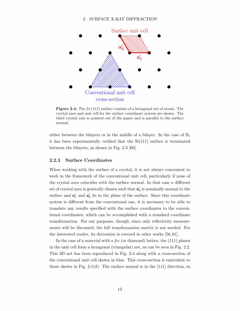
Figure 2.4: The fcc(111) surface consists of a hexagonal net of atoms. Thecrystal axes and unit cell for the surface coordinate system are shown. Thethird crystal axis is pointed out of the paper and is parallel to the surfacenormal.
either between the bilayers or in the middle of a bilayer. In the case of Si,it has been experimentally verified that the Si(111) surface is terminatedbetween the bilayers, as shown in Fig. 2.3 [60].
2.2.3 Surface Coordinates
When working with the surface of a crystal, it is not always convenient towork in the framework of the conventional unit cell, particularly if none ofthe crystal axes coincides with the surface normal. In that case a differentset of crystal axes is generally chosen such that a′3 is nominally normal to thesurface and a′1 and a′2 lie in the plane of the surface. Since this coordinatesystem is different from the conventional one, it is necessary to be able totranslate any results specified with the surface coordinates to the conven-tional coordinates, which can be accomplished with a standard coordinatetransformation. For our purposes, though, since only reflectivity measure-ments will be discussed, the full transformation matrix is not needed. Forthe interested reader, its derivation is covered in other works [56,61].
In the case of a material with a fcc (or diamond) lattice, the (111) planesin the unit cell form a hexagonal (triangular) net, as can be seen in Fig. 2.2.This 2D net has been reproduced in Fig. 2.4 along with a cross-section ofthe conventional unit cell shown in blue. This cross-section is equivalent tothose shown in Fig. 2.1(d). The surface normal is in the [111] direction, so
13

2. SURFACE X-RAY DIFFRACTION
the third crystal axis in the surface coordinate system is
a′3 = a1 + a2 + a3. (2.1)
The standard choice for the in-plane crystal axes is shown with red arrowsin Fig. 2.4 along with the surface unit cell defined thereby. By noting thatthe distance between neighboring atoms in the (111) surface corresponds tohalf of the diagonal of one of the cubic faces of the conventional unit cell[see Fig. 2.1(d)], it should be clear that both of the lengths of each of thesesurface crystal axes is
√2
2 a. Specifically, these vectors are [61]
a′1 =12(a1 − a2)
a′2 =12(a2 − a3).
(2.2)
Thus, the area of the surface unit cell is Acell =√
34 a2. From Eq. (2.1),
the length of the third crystal axis is√
3a. Thus, the volume of the unitcell in the surface coordinate system is 3
4 of the volume of the conventionalunit cell. In the case of a fcc lattice, this means that the surface unit cellvolume encompasses three atoms (compared to the four encompassed by theconventional unit cell volume, as discussed in Sec. 2.2.1). In the case of adiamond lattice, this means the surface unit cell volume encompasses sixatoms, as is evident in Fig. 2.3.
2.3 Diffraction and the Reciprocal Lattice
2.3.1 Bragg Reflections
The phenomenon of x-ray diffraction arises from the coherent interactionof electromagnetic waves scattered from a periodic collection of moleculesor atoms in a crystal lattice. X rays are used because their wavelength ison the order of the interatomic spacing between the atomic constituentsof a solid. Of all the scattered waves, only those scattered elastically willinterfere coherently. Inelastically scattered waves generally all have differentwavelengths and thus contribute to a diffuse incoherent background. Theelastically scattered waves all have the wavelength of the incident radiation,but have different phases based upon the differences in path lengths betweenthe scattering elements in the crystal. Diffraction arises when the scatteredwaves from all (or a macroscopic fraction, anyway) of the atoms in thecrystal have the same phase. There are two historical perspectives to this
14

2. SURFACE X-RAY DIFFRACTION
ki kf
q
d
θθ
d sin θ
Figure 2.5: In the Bragg formalism, x rays reflect specularly from crystal-lographic planes in the crystal. When x rays reflected from different parallelplanes add constructively, one sees a Bragg reflection. The angle θ at whichsuch a reflection occurs is called the Bragg angle. Such a reflection can alsobe described with the momentum transfer vector q in the Laue formalism,in which case the condition for observing a Bragg reflection is when themomentum transfer vector points to a reciprocal lattice point.
phenomenon of diffraction. Both are equally valid and in fact equivalent,but approach it from a slightly different viewpoint.
The viewpoint of Bragg diffraction is based on three assumptions:
Assumption #1. A crystal can be decomposed into parallel lattice planeswith regular interplanar spacings, denoted by d.
Assumption #2. X rays are specularly reflected from these crystallograph-ic planes like light from a mirror.
Assumption #3. At specific angles of reflection, the reflected x rays in-terfere constructively and produce a diffracted beam. These angles withrespect to the crystal planes are called Bragg angles.
This formulation is illustrated in Fig. 2.5, where three successive planes ofatoms in a crystal are shown that have an interplanar spacing of d. Theincident plane-wave x-rays make an angle θ with the planes of the crystaland are reflected specularly. The path length difference between the x raysreflected from the top atomic plane and the one below it is 2d sin θ. For thesewaves to interfere constructively, this path length difference must be equalto an integer number of x-ray wavelengths. Thus, in the Bragg formulation,
15
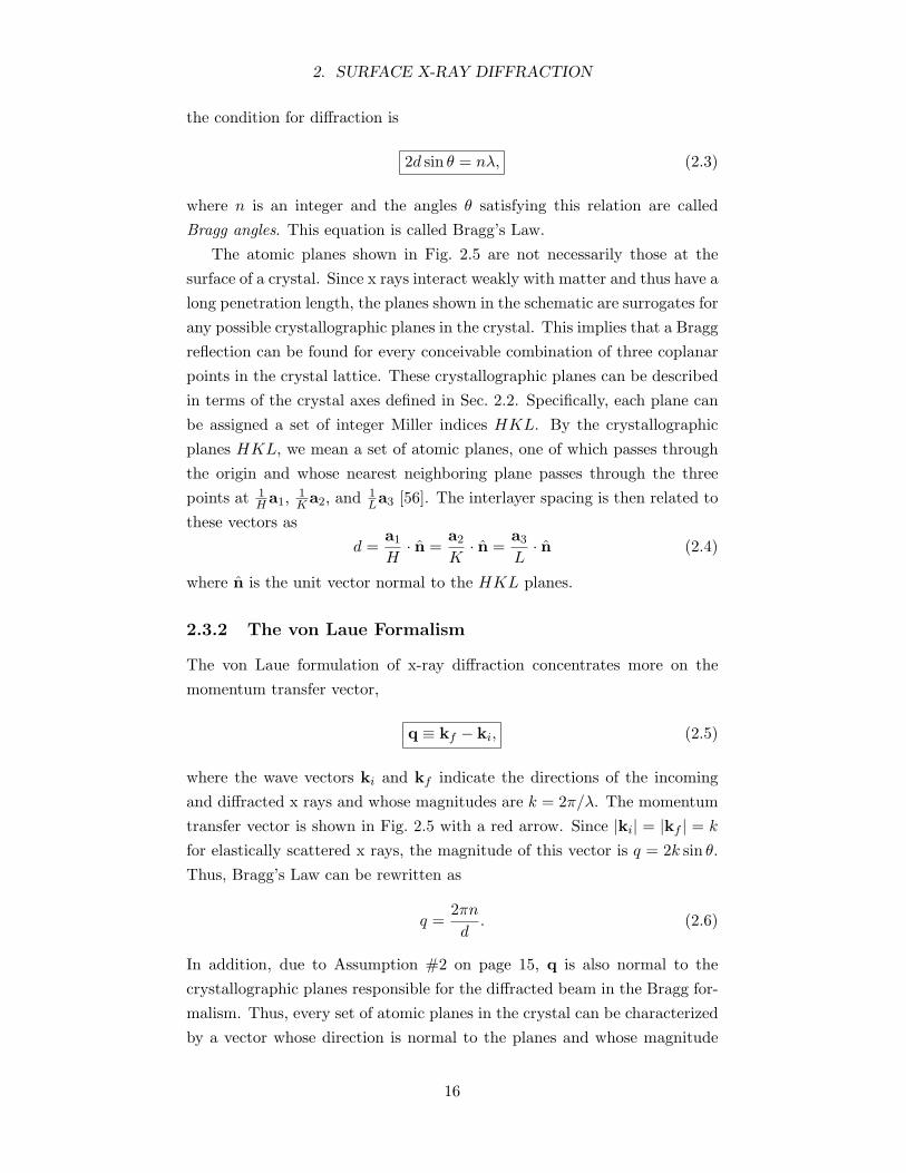
2. SURFACE X-RAY DIFFRACTION
the condition for diffraction is
2d sin θ = nλ, (2.3)
where n is an integer and the angles θ satisfying this relation are calledBragg angles. This equation is called Bragg’s Law.
The atomic planes shown in Fig. 2.5 are not necessarily those at thesurface of a crystal. Since x rays interact weakly with matter and thus have along penetration length, the planes shown in the schematic are surrogates forany possible crystallographic planes in the crystal. This implies that a Braggreflection can be found for every conceivable combination of three coplanarpoints in the crystal lattice. These crystallographic planes can be describedin terms of the crystal axes defined in Sec. 2.2. Specifically, each plane canbe assigned a set of integer Miller indices HKL. By the crystallographicplanes HKL, we mean a set of atomic planes, one of which passes throughthe origin and whose nearest neighboring plane passes through the threepoints at 1
H a1, 1K a2, and 1
La3 [56]. The interlayer spacing is then related tothese vectors as
d =a1
H· n =
a2
K· n =
a3
L· n (2.4)
where n is the unit vector normal to the HKL planes.
2.3.2 The von Laue Formalism
The von Laue formulation of x-ray diffraction concentrates more on themomentum transfer vector,
q ≡ kf − ki, (2.5)
where the wave vectors ki and kf indicate the directions of the incomingand diffracted x rays and whose magnitudes are k = 2π/λ. The momentumtransfer vector is shown in Fig. 2.5 with a red arrow. Since |ki| = |kf | = k
for elastically scattered x rays, the magnitude of this vector is q = 2k sin θ.Thus, Bragg’s Law can be rewritten as
q =2πn
d. (2.6)
In addition, due to Assumption #2 on page 15, q is also normal to thecrystallographic planes responsible for the diffracted beam in the Bragg for-malism. Thus, every set of atomic planes in the crystal can be characterizedby a vector whose direction is normal to the planes and whose magnitude
16

2. SURFACE X-RAY DIFFRACTION
is proportional to the reciprocal of their interplanar spacing in the crystal.Specifically, the unit normal vector in Eqs. (2.4) can be taken to be n = q/q.Together with Eqs. (2.6) and (2.4), this yields the Laue conditions
q · a1 = 2πH (2.7a)
q · a2 = 2πK (2.7b)
q · a3 = 2πL (2.7c)
where by convention the integer n is absorbed into H, K, and L.Thus, every Bragg reflection has a corresponding q vector. Since the
dimensions of q are inverse-length, the mathematical space in which thisvector resides is called reciprocal space. The structure of reciprocal space iscomplementary to that of the real space of the crystal. Specifically, if thebasis vectors of reciprocal space are chosen such that they are orthogonal totwo of the three crystal axes,
ai · bj = 2πδij , (2.8)
then the momentum transfer vector for the Bragg reflection correspondingto the crystallographic planes HKL can be conveniently written as
q = Hb1 + Kb2 + Lb3, (2.9)
which by inspection can be seen to obey the Laue conditions, Eqs. (2.7).The only basis vectors that obey the orthogonality relation, Eq. (2.8),
are
b1 = 2πa2 × a3
a1 · (a2 × a3)(2.10a)
b2 = 2πa3 × a1
a1 · (a2 × a3)(2.10b)
b3 = 2πa1 × a2
a1 · (a2 × a3), (2.10c)
which can be seen from the following example. To construct the basis vectorb1, one first notes that to be orthogonal to both a2 and a3, it must be parallelto a2 × a3. The magnitude of this cross product is the area of the unit cellfacet spanned by the vectors a2 and a3. By Eq. (2.8), the magnitude ofb1 must be inversely proportional to the length of a1 projected onto thevector a2 × a3, which is just the “height” of the parallelepiped defined bythe three crystal axes. Thus, the proper quantity with which to normalize
17

2. SURFACE X-RAY DIFFRACTION
Unit Cell Type Selection Rule (Allowed Reflections)Primitive (Simple) Any H, K,L
Body Centered H + K + L = 2n
Face CenteredH, K, L all odd orH, K, L all even
Diamond(fcc + 2-atom basis)
H, K, L all odd orH, K, L all even and H + K + L = 4n
Hexagonal Close-PackedL even orH + 2K 6= 3n
Table 2.1: Selection rules for common types of crystal lattices. In all cases, nis any integer and H, K, L refer to the bulk-indexed Miller indices of a Braggreflection.
b1 is a1 · (a2 × a3), the volume of the unit cell. This yields the definition ofb1 given by Eq. (2.10a). A similar procedure can be followed for b2 and b3.
The Laue conditions thus describe a 3D lattice of points in reciprocalspace, each of which corresponds to a q vector for a Bragg reflection. Thesepoints are called Bragg points and the lattice formed by these points in recip-rocal space is called the reciprocal lattice. In the case where the crystal axesdescribe a unit cell with a one-atom basis (such as the simple cubic lattice,for instance), every possible combination of integers HKL corresponds toa Bragg peak. However, if the conventional unit cell has multiple identicalatoms in its basis then some HKL combinations may not refer to allowedBragg peaks and are thus termed “forbidden.” This idea can be understoodqualitatively as follows.† Consider for example the fcc conventional unitcell [Fig. 2.1(a)], which has a four-atom basis. Since the reciprocal latticehas the inverse properties of the direct (crystal) lattice, the packing of moreatoms into the real-space unit cell (i.e., denser lattice points) means that thereciprocal space unit cell must have fewer points in it. That is, not everyunit cell in reciprocal space, as defined by the basis vectors bj , will have avalid Bragg point in it. The rules by which one determines which points inthe reciprocal lattice correspond to “allowed” Bragg reflections and whichare forbidden are called selection rules. The selection rules for some basicunit cell types are shown in Table 2.1. For instance, the simple cubic latticehas no forbidden reflections; whereas for the fcc lattice, whose conventionalunit cell is a cube with a basis, only reflections where all the Miller indicesare either even or odd integers are allowed.
†The selection rules for determining which peaks are allowed or forbidden can also bedetermined analytically by constructing the structure factor for the unit cell (Sec. 2.5).See for example, pp. 125–129 in Ref. 55.
18

2. SURFACE X-RAY DIFFRACTION
The selection rules are the result of an additional symmetry in the crystallattice that is not represented in the conventional unit cell. If this additionalsymmetry is broken in some way — e.g., if some of the atoms in the basisare not identical, or they are displaced from their ideal positions — then theselection rules will not necessarily apply. That is, the fcc conventional unitcell has four atoms in it. If these atoms are all identical, then the selectionrule (H, K, and L must be all odd or all even) applies. However, if one ormore of these atoms is different in some way, then the selection rule maybe broken. Similarly, if a material has a unit cell that has additional atomsin its basis, then additional selection rules may apply. For instance, for adiamond lattice, which is a special version of the fcc lattice with twice asmany atoms per unit cell (the primitive unit cell has a two-atom basis), allthe selection rules of fcc apply, plus the additional one that even if H, K,and L are all even, unless they add up to 4n the peak is forbidden.
2.4 Reconstructions and Superperiodicities
In the last section, the inverse nature of the reciprocal lattice was discussedin the context of selection rules. There it was found that if the conventionalunit cell in real space is larger than the primitive unit cell, then there mustbe correspondingly fewer allowed reflections in reciprocal space. That is, ahigher density of lattice points in real space translates to a lower densityof lattice points in reciprocal space. This discussion all took place withinthe context of bulk crystal lattices. The structure of a crystal surface candeviate significantly from the structure of the bulk, though, and truncationof the crystal structure often results in dangling bonds that cause a rear-rangement of the surface atoms into a superstructural configuration. Sucha phenomenon is known as surface reconstruction.
As an example of this effect, consider a crystal surface whose bulk trun-cation would result in a square lattice of atoms. The direct (real-space)and reciprocal lattice along with the respective basis vectors in the surfacecoordinate system are shown in the top portion of Fig. 2.6. Depending onthe details of the atomic structure of the crystal near the surface, the sys-tem may be able to reduce its surface energy slightly by shifting every otherrow of atoms a minute amount in alternating directions, as shown in thebottom portion of the figure. The surface in this case has formed a 2 × 1reconstruction since the surface unit cell has effectively doubled its size inthe a′1 direction.
In Sec. 2.3 it was found that the magnitude of b1 is proportional to
19

2. SURFACE X-RAY DIFFRACTION
⇓ ⇓
Direct Lattice Reciprocal Lattice
2× 1 Reconstruction 1
2-order peaks
a′1
a′2
a′′1
= 2a′1
b′1
b′2
b′′1
= 1
2b′
1
Figure 2.6: Illustration of a surface reconstruction. In this case, simpletruncation of the crystal would result in a square lattice of atoms. Thereciprocal lattice also thus consists of a square lattice of points. However,the lowest-energy configuration of the surface atoms may be such that theyform a superstructure, in this case a 2 × 1 reconstruction. This effectivelychanges the size of the surface unit cell, resulting in corresponding super-structure peaks in reciprocal space.
1/|a1|; thus, an expansion of the effective real space unit cell by a factor oftwo must be accompanied by a shrinkage of the reciprocal space unit cellby a factor of two. This will result in superstructure peaks being found atfractional-order positions in reciprocal space (they are fractionally-orderedwith respect to the original basis vectors, which are still used for indexingpurposes). This effect is illustrated in the bottom portion of Fig. 2.6. Inpractice, since the shifts in atomic positions that cause the reconstructionare usually only very slight, the superstructure peaks are in general muchweaker in intensity than the other peaks.
Although in this example it was assumed that the atoms that form thereconstruction are the surface atoms of a bulk-truncated crystal, such surfacereconstructions can also be induced by one or more layers of adsorbate beingdeposited onto the crystal surface. The effects on the diffraction patterns
20

2. SURFACE X-RAY DIFFRACTION
observed are similar to those described above with the additional complica-tion that the superstructure formed by the adsorbate atoms may be eithercommensurate or incommensurate with the atomic lattice of the crystal sur-face. In the former case, the diffraction features of the adsorbate layer(s)will combine with those due to the underlying crystal lattice and interferencebetween the scattered waves from the two may occur. In the latter case, theadsorbed atoms may form their own independent lattice and/or superstruc-ture that usually have some orientational relationship to the lattice of theunderlying crystal surface, even if they do not share the same periodicity.The diffracted waves from the adsorbate atoms will in general not interferewith those from the underlying substrate in this case, with a notable excep-tion being the case of the reflectivity, which always contains contributionsfrom all the surface layers, regardless of their in-plane orientations. Thereflectivity will be discussed in Secs. 2.5 and 2.6.
The superstructure that is formed by a surface reconstruction, like theone described above, extends in two dimensions in the plane of the crystalsurface. As will be seen in Chapter 5, it is also possible for the structure of acrystal surface or film to have a superperiodic structure along the directionnormal to the surface of the sample. For instance, bilayer oscillations inthe interlayer spacings of the atomic layers of a film will have much thesame effect as the 2× 1 reconstruction shown in Fig. 2.6, except that sincethe superperiodicity lies in the direction of a′3, the superstructure peaks willshow up in the b′3 direction in reciprocal space instead of in the b′1 direction.Conceptually, though, the two effects are analogous — a superperiodicityin the real space lattice results in fractional-order diffraction features inreciprocal space.
2.5 Calculation of the Scattered Intensity
2.5.1 The Structure Factor
Since x rays are wavelike in nature, the scattered intensity from a collectionof particles is calculated by first summing the amplitudes of the waves fromeach individual particle. Once the total amplitude is known, its square mod-ulus is proportional to the measured intensity. The first step in calculatingthe scattered amplitude is to consider a single charged particle. The expres-sion for the cross-section of a charged particle for scattering electromagnetic
21

2. SURFACE X-RAY DIFFRACTION
radiation is given by the Thomson formula [62]
dσ
dΩ= P
(e2
4πε0mc2
)2
, (2.11)
where P is a polarization factor and m is the mass of the scatterer. Sincethe mass of an electron is more than three orders of magnitude smaller thanthe mass of a proton, less than 1/106 of the measured signal will be due toscattering from the protons in the nucleus; thus, it will be subsequently as-sumed that the measured intensity is solely due to scattering from electrons.In that case, this formula can be rewritten as
dσ
dΩ= Pr2
0 (2.12)
where r0 = e2
4πε0mec2= 1.617 × 10⁻⁵ A is called the Thomson scattering
length. The Thomson formula is classical in nature, which in principle issubject to corrections due to the quantum mechanical nature of the photonand scatterer. In particular, when the momenta of the incident and scatteredphotons are different, contributions due to inelastic scattering will occur.Such scattering can either be due to recoil of the electron, in which case it istermed Compton scattering, or in the case of an electron bound to an atomicnucleus, due to the electron making a transition to an excited state of theatom. Compton scattering is diffuse in nature and for our purposes can beconsidered part of the background that is subtracted from the data. In thecase of atomic transitions, as long as the incident x-ray energy is far fromany absorption edges of the material,‡ the corrections due to such effects arenegligible. Therefore, for our purposes, the Thomson formula is an accuratereflection of the electromagnetic cross-section of an electron.
The amplitude of a photon scattered from an electron at position r withrespect to the origin is then
A1 = A0r01
R0eiq·r, (2.13)
where A0 is the amplitude of the incoming plane wave and the factor of1/R0 arises from the spherical nature of the scattered wave. The polariza-tion factor has been left out for the time being and will be reintroduced inSec. 2.5.4. The phase factor of eiq·r is due to the electron not being locatedat the origin. That is, relative to a wave scattered from the origin, the pho-
‡In the field of x-ray diffraction, the energies at which atomic transitions occur arecommonly referred to as absorption edges due to the enormous jump in the absorptioncross-section of the atom at these energies.
22

2. SURFACE X-RAY DIFFRACTION
ki
kf
2θ
r
ki · r −kf · r
Figure 2.7: The geometry for scattering from a single electron. The scat-tered wave picks up a phase of (ki − kf ) · r relative to a wave scatteredfrom the origin. The scattering angle 2θ is defined as the angle between thevectors ki and kf .
ton picks up a phase shift of ki · r along its incoming path and a phase shiftof −kf · r along its outgoing path, as shown in Fig. 2.7; hence, the totalphase factor is e−i(ki−kf )·r = eiq·r. This factor is arbitrary at the moment,since the origin is arbitrary; however, it will be of crucial importance whenmore than one electron is involved and the scattered waves from each parti-cle interfere with one another. Note that since only elastic scattering will beconsidered, |kf | = |ki| = k and the magnitude of the momentum transfer is
q = 2k sin(
2θ
2
), (2.14)
where 2θ is the scattering angle, defined as the angle between ki and kf .As its notation suggests, the scattering angle is related to the Bragg angleintroduced in Sec. 2.3; however, the scattering angle is a more generalizedquantity that need not be related to a Bragg reflection per se. Indeed, wehave yet to build a crystal lattice, without which diffraction cannot arise.
The amplitude from a collection of electrons located at positions rj isjust the sum of those from each individual scatterer, taking into accounttheir different phases,
A = A0r01
R0
∑
j
eiq·rj , (2.15)
where it has been assumed that the distance to the detector is much largerthan the size of the sample volume illuminated by the incident beam; thatis, R0 À |rj |. The scattering from an atom is not simply the scattering froma collection of free electrons, though, so Eq. (2.15) must be generalized to
23

2. SURFACE X-RAY DIFFRACTION
an integral
Aatom = A0r01
R0
∫ρ(r)eiq·rd3r, (2.16)
where the electron density, ρ(r), is described by the quantum mechanicalwave functions of the electrons surrounding the nucleus. In such an integralit is customary to consider the vector origin to be the center of the atom.The integral in Eq. (2.16) is called the atomic scattering factor
f(q) =∫
ρ(r)eiq·rd3r, (2.17)
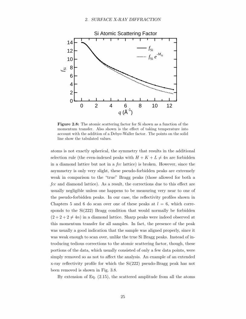
which is the Fourier transform of the electron density of the atom. For verysmall momentum transfers, the exponential factor approaches unity andf(q) → Z, the number of electrons in the atom. In its most general treat-ment, f(q) is a complex quantity dependent on the incident x-ray energy. Ifthe x-ray energy is close to an atomic absorption edge, the Thomson formulano longer adequately describes the cross-section of the electrons in the atomand corrections are necessary. However, since the x-ray energies used in thisstudy were specifically chosen to avoid any such absorption edges, no suchcorrections were made to the atomic scattering factors used. The value ofthe atomic scattering factor as a function of the momentum transfer is tabu-lated for virtually all of the elements of the periodic table [63]. In this work,the values used for the atomic scattering factor were obtained via a cubicspline interpolation of the tabulated values for the neutral atoms. Since theatomic scattering factor varies monotonically and only very slowly, such ascheme yields accurate results. An example of the atomic scattering factoris shown in Fig. 2.8 for Si, which shows the tabulated values as well as theinterpolation curve used.
The atomic scattering factor is written in Eq. (2.17) as a function ofthe magnitude of q since it is almost always spherically symmetric, owingto the approximate spherical symmetry of the core electron density aroundmost atoms. However, deviations from complete spherical symmetry canhave important effects. Most notably, such asymmetries are responsible forviolations of the selection rules for carbon (diamond), silicon, and germa-nium [64]. These materials all form a diamond lattice whose primitive unitcell is that of a fcc lattice with a two-atom basis. As discussed in Sec. 2.3,if the atoms in this basis are identical, an additional selection rule appliesdue to an additional symmetry in the crystal, as shown in Table 2.1. In thecases of carbon, silicon, and germanium, the atoms are identical but theirorientations are slightly different. Since the electron density surrounding the
24
2. SURFACE X-RAY DIFFRACTION
14
12
10
8
6
4
2
0
f Si
121086420q (Å
-1)
Si Atomic Scattering Factor
fSi
fSi e-MSi
Figure 2.8: The atomic scattering factor for Si shown as a function of themomentum transfer. Also shown is the effect of taking temperature intoaccount with the addition of a Debye-Waller factor. The points on the solidline show the tabulated values.
atoms is not exactly spherical, the symmetry that results in the additionalselection rule (the even-indexed peaks with H + K + L 6= 4n are forbiddenin a diamond lattice but not in a fcc lattice) is broken. However, since theasymmetry is only very slight, these pseudo-forbidden peaks are extremelyweak in comparison to the “true” Bragg peaks (those allowed for both afcc and diamond lattice). As a result, the corrections due to this effect areusually negligible unless one happens to be measuring very near to one ofthe pseudo-forbidden peaks. In our case, the reflectivity profiles shown inChapters 5 and 6 do scan over one of these peaks at l = 6, which corre-sponds to the Si(222) Bragg condition that would normally be forbidden(2 + 2 + 2 6= 4n) in a diamond lattice. Sharp peaks were indeed observed atthis momentum transfer for all samples. In fact, the presence of the peakwas usually a good indication that the sample was aligned properly, since itwas weak enough to scan over, unlike the true Si Bragg peaks. Instead of in-troducing tedious corrections to the atomic scattering factor, though, theseportions of the data, which usually consisted of only a few data points, weresimply removed so as not to affect the analysis. An example of an extendedx-ray reflectivity profile for which the Si(222) pseudo-Bragg peak has notbeen removed is shown in Fig. 3.8.
By extension of Eq. (2.15), the scattered amplitude from all the atoms
25
2. SURFACE X-RAY DIFFRACTION
in the unit cell of a crystal is
A = A0r01
R0F (q) (2.18)
whereF (q) =
∑
j∈cell
f(q)eiq·Rj (2.19)
is called the structure factor, since it describes the geometrical arrangementof the atoms in the unit cell. The sum in this expression is over all the atomsin the unit cell, each positioned at Rj with respect to the cell origin. Sincethis arrangement is usually not spherically symmetric, F (q) is in generala function of the vector q, unlike the atomic scattering factor. Just as theatomic scattering factor is the Fourier transform of the electron density of anatom, the structure factor is the Fourier transform of the electron density ofa crystal’s unit cell. Since the unit cell is the fundamental entity or buildingblock of a crystal, F (q) is the primary quantity representing the atomicbasis of the crystal structure. For this reason, the structure factor plays aprominent role in x-ray crystallography.
In the case of a film, the presence of lattice relaxations or distortions inthe film structure often results in the interlayer spacings being dependent ontheir vertical positions in the film. For this reason, when deriving a modelto describe the scattered amplitude from a film, the structure factor for thefilm is often taken to extend the entire film thickness, with the positions ofthe individual atomic layers in the film described by separate parameters(see Sec. 2.6.3).
2.5.2 Diffraction from a 3D Crystal
The total scattered intensity from a crystal is proportional to the sum ofthe amplitudes from all the crystal’s unit cells. It is the combined ampli-tude from the symmetric arrangement of a large number of unit cells in thecrystal that focuses the scattered x-rays into distinct beams, resulting in thephenomenon that is commonly referred to as diffraction. For simplicity ofdiscussion, it will be assumed that the crystal consists of a parallelepipedwith N1, N2, and N3 unit cells in the directions of the three crystal axesa1, a2, and a3, respectively. However, the arguments that follow are equallyvalid regardless of the shape of the crystal in question [56]. The scattered
26
2. SURFACE X-RAY DIFFRACTION
amplitude from all these unit cells is
Axtal = A0r01
R0F (q)SN1(q · a1)SN2(q · a2)SN3(q · a3) (2.20)
where SN (x) is the geometric sum
SN (x) =N−1∑
n=0
eixn (2.21)
=1− eixN
1− eix. (2.22)
Since the measured intensity will be proportional to the square modulus ofthe amplitude, the quantity of interest is
∣∣SN (x)∣∣2 =
sin2(
12Nx
)
sin2(
12x
) , (2.23)
which is called the N -slit interference function. An example of this functionis shown in Fig. 2.9 for N = 10. As can be seen, it consists of N − 2interference fringes between two large peaks whose heights scale as N2 andwidths scale as 1/N . In the limit, N →∞, the N -slit function tends to anarray of Dirac delta functions spaced by 2π in x. In the case of a bulk crystal,N1, N2, N3 → ∞ and Eq. (2.20) is zero everywhere except when the Laueconditions, Eqs. 2.7, are satisfied simultaneously. The large peaks in theN -slit interference function of Fig. 2.9 are thus the Bragg peaks describedin Sec. 2.3.
Since the intensity is proportional to the square modulus of the scatteredamplitude, it can be concluded that the diffraction pattern from a 3D crystalis zero everywhere except at discrete points that lie on a lattice in reciprocalspace, where the intensity is
IHKL ∝∣∣∣∣A0r0
1R0
F (Hb1 + Kb2 + Lb3)N1N2N3
∣∣∣∣2
. (2.24)
This equation is written as a proportionality relationship since there are anumber of experimental corrections that must still be taken into account,which will be detailed in Sec. 2.5.4. However, first a discussion of the differ-ences between the diffraction from a 3D crystal and a 2D film is in order.
27

2. SURFACE X-RAY DIFFRACTION
0
2
2π/N
0 π 2π
2|
|2
(a)
(b)
-Slit Interference Function
Figure 2.9: The N -slit interference function for N = 10 on (a) a linearscale and (b) a log scale. The heights of the main peaks scale as N2, theirwidths as 1/N , and they become Dirac delta functions as N →∞.
2.5.3 Diffraction from a Film
The conditions for constructive interference (diffraction) from a 3D crystalresult in a lattice of Bragg points in reciprocal space defined by the Laueconditions. However, in the case of a film, the crystal is only large in twoof the three dimensions. We will operate in the surface coordinate systemof the film, as described in Sec. 2.2, where a′3 is directed along the surfacenormal (the z direction) and a′1 and a′2 both lie in the plane of the film andare thus perpendicular to a′3. In this case, N1, N2 → ∞, and N3 = N isthe number of layers in the film (a film of uniform thickness is assumed forthe time being). Then the third Laue condition, Eq. (2.7c), is relaxed andthe (former) points in reciprocal space defined by Eqs. (2.7a) and (2.7b)each have a profile like that of Fig. 2.9 extending in the z direction. These
28

2. SURFACE X-RAY DIFFRACTION
features are called “rods” due to their one-dimensional nature in reciprocalspace. In fact, such rod-like features are found around the Bragg pointsof bulk crystals as well, provided the crystal surface is sharp enough. Forthis reason, these features are often referred to as crystal truncation rods(CTRs) [65].
Regardless of the in-plane structure of the film and substrate, thereis always a CTR for H = K = 0; that is, when q is aligned along thesurface normal (q · r = qzz). This CTR is the specular rod and it offers auseful probe of the structural features normal to the surface — for example,vertical layer relaxations — without concern for the details of the lateralstructure of the film or substrate. Such measurements are valuable wheneffects due to the lateral structure or in-plane order of the sample are not theprimary focus. Although off-specular rods in principle collectively containmore information than the specular rod alone, if the in-plane structure of thefilm or substrate is not well-ordered, or if it is different for different portionsof the film, the intensity along these rods will either be diffuse or dividedamong different regions of reciprocal space (e.g., different surface domainsmay have different in-plane orientations). In contrast, the reflectivity rodcontains contributions from all the film overlayers regardless of their in-plane structure, and absolute information on vertical layer relaxations andfilm thicknesses can be obtained. It should be noted that unlike off-specularrods in most cases, the specular rod always contains contributions from boththe substrate and the film overlayers. Thus, the scattered amplitudes fromboth must be added together to calculate the intensity along this rod.
For small momentum transfers (q ¿ 2π/a′3), the intensity along thespecular rod is termed the x-ray reflectivity. It is relatively insensitive to thediscrete atomic nature of the film and may include dynamical effects [54,55].For higher momentum transfers, diffraction effects due to the crystallinestructure of the film and substrate are evident. The rod profile in thisregime is thus termed the extended x-ray reflectivity. To obtain informationon the atomic-layer structure of the sample, large momentum transfers mustbe measured. Thus, for a study of lattice relaxations in film overlayers, ormeasurement of the distribution of film thicknesses present with atomic-layer resolution, the extended reflectivity is the appropriate portion of therod to measure.
29

2. SURFACE X-RAY DIFFRACTION
2.5.4 Geometrical Correction Factors
The measured intensity is proportional to the square modulus of the to-tal scattered amplitude. However, the simplified treatment presented thusfar ignores many of the experimental realities of measuring scattered x-rayintensities. The combined effects of these geometry-dependent correctionfactors will be denoted with the symbol C and can be broken up into thecomponents [66]
C = P CLCRCA (2.25)
where P is the polarization factor, CL is the Lorentz factor, CR is the rodinterception factor, and CA is the beam footprint area correction factor, allof which will be discussed below. Since these corrections are all specific tothe scattering geometry chosen in the experiment, they in themselves do notcontain any information about the structure of the sample. For this reason,and for simplicity of analysis, these geometric corrections were applied to theexperimental data before analysis. Thus, most of the x-ray data presentedin this work are the experimentally measured intensities divided by C.
The other corrections discussed in this section are those due to temper-ature effects and those due to surface roughness. As will be seen, theseeffects have more to do with the details of the physical state and structureof the sample and therefore must in general be taken into account at thelevel of the structure factor calculation. Furthermore, additional correctionsto the raw data may be necessary depending on the type of detector usedand the absolute intensity of the scattered x-rays. Such corrections will beseparately discussed in Sec. 3.3.2.
Polarization factor
The factor P introduced in Eq. (2.12) results from the different polariza-tions of the incoming and outgoing x-ray beams. Specifically, P = |εi · ε∗f |2,where εi and εf denote the polarization vectors for the incident and scat-tered waves, respectively. In this work, synchrotron radiation was usedexclusively to obtain the x-ray diffraction data. The x rays produced froma synchrotron result either from the emission of radiation as the electronsorbit around the synchrotron ring (bending magnet source) or from the hor-izontal “wiggling” motion produced as the electrons pass through a series ofvertically-oriented permanent magnets placed in the path of the electrons(an insertion device). In any case, the acceleration of the electrons is al-ways in the horizontal plane and hence the emitted x rays will be linearly
30

2. SURFACE X-RAY DIFFRACTION
polarized in the horizontal plane as well.§ The polarization factor is thusP = cos2 ψ, where ψ is the angle between ki and the projection of kf ontothe horizontal plane. For the experiments done in this study, the scatteringplane (the plane formed by ki and kf ) was always horizontal, so in our caseψ = 2θ and
P = cos2(2θ). (2.26)
To avoid any confusion, it should be noted that most texts quote thepolarization factor as
P ′ =1 + cos2(2θ)
2, (2.27)
which is true if the incident x rays are unpolarized. This expression can beeasily obtained by noting that if the experiment had been set up such thatthe scattering plane were vertical, then the polarization factor would havebeen P = 1. Quantum mechanically, unpolarized x-rays are in a superpo-sition of two arbitrary orthogonal polarization states, which can be chosento be aligned and perpendicular to the scattering plane, respectively. Thescattered x-ray intensity is then the average of the scattering from the twodifferent polarization states, which yields Eq. (2.27).
Integrated intensity and the Lorentz factor
One would normally assume that the intensity as calculated in the previ-ous sections would be an observable quantity; however, a number of exper-imental realities make measurement of such intensities impossible. Sampledefects and mosaicity, finite energy resolution of the monochromatic source,and angular dispersion of the incident beam will all result in a finite spread-ing of the scattered beam. As a result, in practice the intensity of either a2D or 3D region of reciprocal space is measured. This quantity is called theintegrated intensity and is usually measured by scanning an angle with thediffractometer while measuring the scattered intensity. Hence, the actualintegration is done in angular space, which must be converted to recipro-cal space to compare it with theoretical models. This can be done using astandard coordinate transformation for the appropriate diffractometer andgeometry [56, 66–68]. In the end, the integrated intensity is found to berelated to the peak intensity by a factor called the Lorentz factor, whichis equal to the inverse of the Jacobian of the transformation from angularspace to reciprocal space. For measurements along the specular rod, the
§A notable exception to this rule exists in which a specialized undulator can be con-structed to produce circularly polarized x-rays. However, such devices are rare and werecertainly not used in this study.
31

2. SURFACE X-RAY DIFFRACTION
Lorentz factor is simply [66,67]
CL =
1sin(2α) (rocking curve)
1sin α (ridge scan)
(2.28)
where α is the angle the incident x-ray beam makes with the sample sur-face and the terms “rocking curve” and “ridge scan” refer to two differentmethods of measuring the specular rod to be discussed in Sec. 3.6.
Rod interception factor
The rod interception factor is related to the manner in which a diffrac-tion rod from a 2D or quasi-2D system is experimentally measured. Thesetechniques are discussed in detail in Sec. 3.6, when the origin of the rod in-terception factor will be illustrated more clearly. However, a brief discussionof the correction it entails is presented here for the sake of completeness.
The acceptance area of the detector is usually defined using a pair ofslits. Such slits are generally perpendicular to each other and to the direc-tion of the x-ray beam being measured. With the rocking curve method ofmeasuring the integrated intensity of the specular rod, these detector slitsare scanned across the specular condition to obtain a cross-sectional pro-file of the rod from which the background and integrated intensities can bedetermined. The resulting integration volume from such a procedure sam-ples a slice of the specular rod that has a finite thickness in the z directionand that varies depending on the slit settings and angles of incidence andreflection (see Fig. 3.11). Specifically, the thickness of the cross-sectionalslice is proportional to cosβ, where β is the angle the scattered x rays makewith the sample surface [see Eq. (3.9)]. Hence, as the intensities at differentplaces along the specular rod are measured (using the same slit settings),the magnitude of the integrated intensity varies as
CR = cosβ. (2.29)
This factor is only necessary for data collected using the rocking curvemethod.
Beam footprint area
The measured intensity from a diffraction feature of a film will be pro-portional to the illuminated area of the sample. Actually, the area of the
32
2. SURFACE X-RAY DIFFRACTION
sample that will contribute to the signal measured is the intersection of theprojected areas of the beam footprint on the sample and the areal accep-tance of the detector being used. In addition, angular dispersion of thesource x-ray beam and finite angular acceptance of the detector should inprinciple also be accounted for [66, 67]. However, in practice, the detectorslit settings are generally chosen such that the entire illuminated area ofthe sample is accepted, and with modern beamline optics and proper col-limation of the scattered beam, angular dispersion is usually negligible. Inparticular, for the specular geometry, in which the beam footprint seen fromthe perspective of the detector is simply the incident beam profile (usuallyon the order of 0.5 mm× 0.5 mm), acceptance of the fully collimated beamby the detector is generally not a problem and the correction factor can beregarded as equal to the illuminated area of the sample. Assuming thatthe sample subtends the entire width of the beam, the area of the beamfootprint in a specular geometry is proportional to
CA =1
sinα(2.30)
where α is the angle the incident x rays make with the sample surface.
Debye-Waller factor and TDS
So far, it has been assumed that the atoms occupy fixed positions withinthe crystal lattice. However, thermal fluctuations in the atomic positions willbe present at any finite temperature. Two effects arise from these thermalvibrations. First, a Debye-Waller factor of the form e−M must be includedin the structure factor, where M ≡ 1
2 〈q · u〉2 and u is the displacementvector of the atoms from their equilibrium positions in the crystal due tothermal vibrations [56]. Since atoms of different materials will respond dif-ferently to thermal excitations, M will be dependent on both temperatureand material. Thus, a unit cell that contains atoms of many different typeswill need to have the correct Debye-Waller factor applied to each atom inthe structure factor. For this reason it is often most appropriate to applythe Debye-Waller factor directly to the atomic scattering factors. Althoughtheoretically-derived values for the Debye-Waller factor are available [69], inthe case of a film, where the response of the atoms to thermal excitations isnot necessarily the same as their bulk counterparts, it is generally left as afree parameter that is determined from a fit to the experimental data. Anexample of the effect the Debye-Waller factor has on the atomic scattering
33
2. SURFACE X-RAY DIFFRACTION
factor of a Si atom can be seen in Fig. 2.8.Of course, the vibrations of the atoms in a crystal are not isotropic,
but are subject to the spectrum of different phonon modes for the material.This fact results in a second temperature-related phenomenon called thermaldiffuse scattering (TDS). In terms of effects on the scattered intensity, TDSappears as a series of broad diffuse peaks in reciprocal space emanating inhigh-symmetry directions from the Bragg points. As such, TDS does notinterfere much with the comparatively sharp diffraction features presentedin this work and can be considered part of the background that is subtractedfrom the signal.
Roughness
There are two different mtehods that can be used to account for theroughness of a sample surface. First, a simple model of the statistical prop-erties of the surface roughness can be assumed and the results on the mea-sured intensity profile calculated analytically. This method has been shownto work well for a variety of different surfaces by assuming an exponentialdistribution of heights on the surface [65]. In this model, layer 0, at thelowest (inner) end of the roughness boundary region, is assumed to be fullyoccupied, layer 1 right above it has a fraction β of sites occupied (not to beconfused with the angle β), layer 2 has fraction β2, etc. The intensity fromsuch a surface is related to the ideally truncated surface by an additionalmultiplicative factor
Irough = Iideal(1− β)2
1 + β2 − 2β cos(q · a3). (2.31)
Alternately, the distribution of heights present on the surface can be de-scribed explicitly, with the relative site occupancy of the different layers inthe boundary region included as free parameters to be determined by a fitto the experimental data. Such a method requires a diffraction profile withenough information that the free parameters are sufficiently constrained.
In the case of a supported film, there are two physical regions in whichroughness is present. First, the thickness of the film itself (i.e., the num-ber of atomic layers on top of the substrate) will not be perfectly uniform,resulting in a distribution of thicknesses. In our case, it will be found thatthe lattice structure of the film overlayers is itself thickness-dependent, sothe surface morphology must be described explicitly. Since the films studiedwill have thicknesses less than 20 AL, the intensity along the specular rodwill have a rich structure with enough information to determine the film
34

2. SURFACE X-RAY DIFFRACTION
roughness explicitly, following the second method outlined above. Second,the underlying substrate on which the film is grown is not a perfectly flatsurface. Since this roughness is due to statistical variations related to thesample preparation, it can be described using Eq. (2.31). However, cleanSi(111) surfaces have been found in previous studies to have very small de-grees of roughness [65], which was also found to be the case in this study,where the data analysis was found to be unaffected by inclusion of such afactor.
2.6 Extended Reflectivity of a Pb/Si(111) Film
2.6.1 Overview
In this section, the formulas derived in the previous sections of this chap-ter are applied to generate explicit equations for the extended reflectivityof a Pb/Si(111) film. These equations will then be used in a least-squaresalgorithm in Chapters 5 and 6 to fit experimental data. Since we are onlyconcerned with the specularly reflected intensity, the momentum transfervector is parallel to the surface normal (the z direction). Using the surfacecoordinate system described in Sec. 2.2.3, q · a1 = q · a2 = 0 and the scat-tering amplitude is dependent only on qz. Thus, only the positioning andrelative occupancy (density) of the atomic planes of the film and substratein the z direction affect the reflectivity. By convention, the momentumtransfer is specified using the reciprocal lattice units of the substrate; hence,in this work, the momentum transfer will be quoted with the index l, theperpendicular momentum transfer in Si(111) reciprocal lattice units (1 r.l.u.= 0.668 A−1):
l =aSi
√3
2πqz. (2.32)
Using this convention, the Si(111) Bragg peak will appear at l = 3, whereassince Pb has a lattice constant roughly 10% larger than Si, the Pb(111)Bragg peak will appear at l ≈ 3.3.
Two distinct surface morphologies were encountered in the experiments.In Chapter 5, films were grown at 110 K in progressive steps, where thethickness of the film was varied by deposition of additional Pb on the sam-ple surface. In these experiments, the film growth was found to follow alayer-by-layer mode in which closed films form with low degrees of rough-ness. Since the temperature was held constant, the film morphology waseffectively frozen in place and can be considered to be more-or-less uniform
35

2. SURFACE X-RAY DIFFRACTION
over large lateral distances. An intensity calculated assuming only coherentcontributions to the intensity is appropriate for such a morphology.
In contrast, Chapter 6 presents experiments where the Pb depositionwas only done once per sample. After deposition, the films were annealedto progressively higher temperatures. Eventually, the additional thermalenergy is enough that the atoms on the sample surface begin to rearrangethemselves into nanostructures that are more stable than the closed filmspresent immediately after deposition. If the distances between such struc-tures is large enough, an incoherent contribution to the measured intensitymay be discernible. In this case, the total intensity results from the incoher-ent addition of the scattered intensities from different regions of the surface.The formula for the reflected intensity differs somewhat for such a sample,with the introduction of a partial coherence factor necessary.
2.6.2 Substrate Amplitude Contribution
Since the reflectivity rod of the film overlayers coincides with that of thesubstrate, the scattered amplitudes from the two must be added together.All the substrates in this study were pretreated by a method that has beenshown to result in a bulk-truncated Si(111) surface (see Sec. 3.5.2). Ignoringfor the time being any lattice relaxations near the surface of the Si crystal,the contribution of the substrate to the scattered amplitude is that of asemi-infinite crystal truncated at z = 0 and extending in the −z direction
ASi(qz) ∝ σSiFSi(qz)∞∑
j=0
e−iqzaSi
√3j , (2.33)
where σSi is the atomic density of a Si(111) plane, aSi
√3 is the length of the
unit cell in the [111] direction, and FSi(qz) is the structure factor of Si asa function of the perpendicular momentum transfer. In the [111] direction,the Si unit cell consists of three equally spaced bilayers, with the interlayerspacing within each bilayer being 1
12 of the total unit cell length (see Fig. 2.3).For the purpose of calculating the reflectivity, the different in-plane atomicarrangements of the three bilayers in each unit cell are immaterial and thethree bilayers can be treated identically. Thus, the reflectivity structurefactor for Si is
FSi(qz) = fSi(qz)e−MSi
(1 + e−iqzaSi
√3/12
)
×(1 + e−iqzaSi
√3/3 + e−iqzaSi2
√3/3
)(2.34)
36

2. SURFACE X-RAY DIFFRACTION
d23
d12
N Layers N + 1 Layers
......
......
......
zN−3
zN−2
zN−1
zN
zN+1
Figure 2.10: Roughness in the film will manifest itself at the atomic scaleas a distribution of thicknesses N. Since the relaxation of each atomiclayer will depend on its position relative to the film boundary, the posi-tions of the layers from regions of different thicknesses will tend to differ.To account for this effect in the reflectivity, either the exact positions ofthe layers for each region of thickness need to be known, or an effectivedistribution in z can be used analogous to a Debye-Waller factor.
where the first term in parentheses is due to the interlayer spacing withineach bilayer and the second is the three instances of the bilayer per unit cell.Equation (2.33) then becomes
ASi(qz) ∝ σSifSi(qz)e−MSi
(1 + e−iqzaSi
√3/12
) ∞∑
j=0
e−iqzaSi
√3j/3 (2.35)
= σSifSi(qz)e−MSi1 + e−iqzaSi
√3/12
1− e−iqzaSi
√3/3
. (2.36)
The presence of lattice relaxations in the top substrate layers can be takeninto account by adding additional Si layers to this amplitude that haveadjustable vertical positions. Such an effect was included in analysis ofsome of the data; however, due to the much greater electron density of thePb overlayers it was found that effects due to lattice relaxations of the topSi layers were not observable. As such, all of the results presented do notinclude any parameters describing substrate layer relaxations.
2.6.3 Film Structure Factor
Allowing for possible lattice distortions in the film in the direction of thesurface normal, the amplitudes from all the film layers will be included inthe structure factor of the film. The scattered amplitude from the film is
37

2. SURFACE X-RAY DIFFRACTION
thenAPb ∝ σPbFPb(qz) (2.37)
where σPb is the atomic density of a bulk Pb(111) layer. Note that sinceSi has a diamond lattice structure and Pb has a fcc lattice structure, their(111)-surface atomic densities are related by
σPb
σSi=
(aSi
aPb
)2
. (2.38)
Following prior work in the literature, the structure factor for the film isusually written as [60,70]
FPb(qz) = fPb(qz)Nmax∑
j=1
θjeiqzzje−
12q2zζ2
j (2.39)
where Nmax is the number of atomic layers in the thickest portion of the filmand θj is the fractional occupancy of layer j. The last exponential term issimilar to a Debye-Waller factor and accounts for a finite layer distribution inz, where ζj is the root-mean-square displacement of the atoms in layer j fromtheir average position, zj , which is measured relative to the Si surface. Thisterm is particularly important in systems with substantial lattice relaxationssince the atomic layers in regions of different thicknesses will in general notline up. This effect is expected to be larger for near surface layers, asillustrated in Fig. 2.10. The ζj values for these layers will have a significantcomponent due to the static displacements of the layers in different regions,resulting in a value that depends on j. For films with significant roughness— i.e., with a wide range of thicknesses — the number of independent zj ,θj , and ζj parameters can become quite large.
Alternatively, in a model that describes the film layer structure moreprecisely, where the zj parameters are different for each thickness N , the ζj
parameters will be approximately independent of j and can be taken outsidethe sum as a standard Debye-Waller factor e−MPb . In such a model, the filmcontribution to the structure factor is written as
FPb(qz) = fPb(qz)e−MPb∑
N
pN
N∑
j=1
eiqzzj,N (2.40)
where pN is the fractional surface area covered by N Pb layers and the first
38

2. SURFACE X-RAY DIFFRACTION
sum is over all thicknesses present in the film. That is,
θj =∑
N≥j
pN , (2.41)
and ∑
N
pN = 1. (2.42)
In this scheme, the coverage of the film, which is proportional to the totalnumber of Pb atoms in the film and is measured in AL of Pb,∗ is
Θ =∑
N
NpN . (2.43)
Generalizing the zj values to be N -dependent will add numerous addi-tional parameters if they are taken as independent degrees of freedom, whichcan substantially complicate the data analysis. To avoid this difficulty, aphysical model is derived in Sec. 4.4 that describes the lattice distortions.From this model, the zj,N are calculated using only a small number of ad-justable parameters, eliminating most of the independent variables. Thismodel for the x-ray reflectivity has far fewer degrees of freedom than themodel using Eq. (2.39), yet was found to reproduce the results with a sim-ilar degree of precision, indicating that the zj,N values calculated with thelattice distortion model accurately reflect the actual film morphology.
2.6.4 Calculation of the Measured Intensity
As discussed in Sec. 2.6.1, any sample will have regions of different thick-nesses. If the lateral distances between these regions is much smaller thanthe coherence length of the scattered x rays, the integrated intensity is pro-portional to the coherent sum of the contributions from the substrate andthe Pb overlayers
Icoh(qz) ∝ C ∣∣ASi(qz) +APb(qz)∣∣2, (2.44)
where C is given by Eq. (2.25). Equation (2.44) is written as a proportion-ality relationship since in practice only the relative intensity is measured;thus, an arbitrary scale factor must be included when comparing theoreticalcalculations with empirical measurements.
∗In other texts, coverages are often quoted in “monolayers”, which may be relative tothe atomic surface density of either the film or substrate. Here the unit of “atomic layer”is used, which is less ambiguous. In terms of coverage, 1 AL is equal to a monolayer inPb units.
39

2. SURFACE X-RAY DIFFRACTION
Inte
nsity
(ar
b. u
nits
)
76543l (r.l.u.)
Λ=1 (Coherent) Λ=0
(a)
(b)
Figure 2.11: Examples of the extended reflectivity for two different Pbfilms on Si(111) substrates. The intensities using both the coherent andincoherent calculations are shown. (a) A film with a significant degree ofroughness (5.7 A rms). Few interference fringes are present between the PbBragg peaks at l ≈ 3.3 and 6.6. (b) A film with a low degree of roughness(2.3 A rms). More interference fringes are evident, with the profile verysimilar to the ideal N -slit interference function shown in Fig. 2.9(b). Tak-ing into account the incoherent addition of regions of different thicknessestends to raise the relative intensity of the profile between the Bragg peaksand diminish the interference fringes. In both cases, the distribution ofthicknesses used to calculate the profiles, which include a wetting layer, isshown in the insets.
40

2. SURFACE X-RAY DIFFRACTION
If regions of different thicknesses are separated by significant lateral dis-tances, the reflected intensity will have a component due to incoherent scat-tering from these different regions. In the extreme case, where all the thick-ness regions add up incoherently, the total intensity is the weighted sum ofthe intensities from each separate region, which consists of a single heightisland surrounded by a wetting layer. Since the wetting layer fills in thespace between the different thickness regions, it will contribute coherentlyin each case. The structure factor for a region with islands that are N layersthick surrounded by the wetting layer is thus
FNPb(qz) = fPb(qz)e−MPb
p1e
iqzz1 + (1− p1)N∑
j=1
eiqzzj,N
(2.45)
and the total scattered intensity is the incoherent sum of the intensities fromeach individual thickness region is
Iincoh(qz) ∝ C∑
N>1
pN
1− p1
∣∣∣ASi(qz) + σPbFNPb(qz)
∣∣∣2. (2.46)
Note that in the ideal case where the surface consists of islands of only onethickness separated by regions covered only by the wetting layer, Eq. (2.45)reduces to Eq. (2.40) and Eq. (2.46) reduces to Eq. (2.44); i.e., the incoherentand coherent intensities are equivalent, as one would expect.
In actuality, the reflected intensity is likely some combination of coherentand incoherent scattering from regions of different thicknesses, in which casethe measured reflected intensity is
I(qz) = ΛIcoh(qz) + (1− Λ)Iincoh(qz) (2.47)
where Λ is a partial coherence factor (0 ≤ Λ ≤ 1), which is treated as afitting parameter in the analysis. The calculated extended x-ray reflectivityfor two different Pb films is shown in Fig. 2.11 to illustrate the effects ofroughness and the coherence factor on the rod profile. In this graph, the re-flectivity is plotted as a function of l, as defined in Eq. (2.32). Figure 2.11(a)shows the reflectivity profile for a rough film (5.7 A rms), with the pN dis-tribution shown in the inset. Both the coherent (solid curve) and incoherent(dotted curve) intensities are shown. The main features in both cases arethe Si(111) Bragg peak at l = 3 and the Pb(111) and (222) Bragg peaks atl ≈ 3.3 and 6.6, respectively. In between the Pb Bragg peaks are relativelyfew fringes due to the significant film roughness. In contrast, the calcula-
41

2. SURFACE X-RAY DIFFRACTION
tion for a smooth film (2.3 A rms), shown in Fig. 2.11(b), exhibits morepronounced interference fringes very similar to the N -slit function profile inFig. 2.9(b). From this figure two primary effects due to the coherence factorare apparent. First, the ratio between the intensities at the in-phase (Braggpeaks) and out-of-phase conditions (midway between the Bragg peaks) forPb is different, with the incoherent profile being on average more intensethan the coherent profile. Second, the interference fringes are more pro-nounced in the coherent calculations than the incoherent ones.
42

3 Experimental Methods
3.1 Introduction
This chapter provides an overview of the methods and equipment that wereused in the experimental portion of this work. Since all of the experimentsinvolved the preparation of the samples in an ultrahigh vacuum (UHV)environment, a brief introduction to this technology as well as a general de-scription of the vacuum setup used will be given. However, since a completeunderstanding of vacuum technology and UHV hardware is not necessaryto understand the results presented here, the focus will be primarily on theequipment and procedures used specifically in the experiments described inthis work. The interested reader is directed to other sources [71–73] for amore comprehensive discussion of UHV technology and its applications.
Next, various different methods and instruments used to detect x raysare described. Although there exists a wide range of sophisticated detectorsto choose from [74–76], the discussion in this chapter will focus on thosethat were used in this study, which were all single-channel photon counters(point detectors).
Since x rays interact weakly with matter, the use of a high-brilliancesynchrotron source is all but necessary to do high-resolution atomic-scalestudies. All of the experimental data in this work were collected usingmonochromatic x rays from an undulator source at a third-generation syn-chrotron storage ring. This facility and the experimental equipment usedthere are described along with a brief overview of how the x-ray beam isgenerated and produced.
Then the methods used to prepare the samples and to grow the metalfilms are discussed. In particular, it was found that a pretreatment of thesemiconductor substrates greatly improved the quality of the metal films.The resultant films after deposition have near-atomic uniformity in thicknessthat enables monolayer-resolved studies to be done. Such a pretreatmentalso results in a bulklike truncation of the Si substrate which simplifies theanalysis and provides a sharp buried interface that enhances the quantumconfinement effects that will be studied.
43

3. EXPERIMENTAL METHODS
Finally, two different techniques for measuring the x-ray reflectivity rodare presented. The rocking curve method provides highly accurate dataover the widest range of momentum transfer and is traditionally the onemost widely used for high-resolution CTR measurements; however, it re-quires a great deal of time to acquire a single set of data. Due to the timeconstraints on experiments at a synchrotron facility, such a time-consumingmethod makes a study difficult when the measurements need to be repeatedfrequently for the same physical sample. The ridge scan method of collectingthe extended x-ray reflectivity solves this problem by collecting the entirereflectivity rod in just 1–3 scans, which greatly reduces the amount of timeneeded to acquire a single set of data. Both methods have certain limitationsand advantages over the other that will be discussed in detail. For the rangeof momentum transfer studied in this work the two methods were found toyield equivalent data.
3.2 Ultrahigh Vacuum
3.2.1 Characteristics
For a study of the atomic-scale properties of surfaces, precise control of thepreparation and cleanliness of the sample surface is essential. Since a surfaceby definition is exposed to the ambient environment, it is always subject tocontamination. In the case of a reactive surface, residual gas atoms maychemically bond with exposed atoms at the surface to form molecular com-pounds of the material that are not desired (an oxide layer, for instance).However, even an inert sample will have condensed layers of gas atoms ormolecules adsorb onto it. Herein lies the utility of a vacuum chamber. Byremoving the bulk of the ambient gas in a controlled environment, a samplesurface can be kept clean for an extended period of time during which it canbe manipulated in a controllable and repeatable manner to study the physi-cal processes at work. Depending on the application to be performed on thesurface, different pressure ranges are needed. The highest degree of vacuum(i.e., with the lowest ambient pressure) is termed ultrahigh vacuum and itrequires special procedures and equipment to produce and maintain. Thedifferent classes of vacuum and their pressure ranges are shown in Table 3.1.
Although the Systeme International unit of pressure is the Pascal (N/m2,abbreviated as Pa), traditionally in high-vacuum science the unit of torr(mm Hg) is used, named after Evangelista Torricelli (1609–1647), the inven-tor of the mercury barometer and a contemporary of Galileo. Another unit
44

3. EXPERIMENTAL METHODS
Name PressureRange (torr)
MonolayerFormation Time (s)
Mean FreePath (m)
Low (Rough) 760 – 10−3 10−9 – 10−4 10−6 – 10−2
High 10−3 – 10−8 10−4 – 10 10−2 – 104
Ultrahigh 10−8 – 10−9 10 – 500 104 – 105
10−9 – 10−10 500 – 104 105 – 106
< 10−10 > 104 > 106
Table 3.1: Various pressure ranges and some of the typical characteristics of thevacuum environment in those ranges. All values should be taken as approximateorders of magnitude for a typical vacuum system.
that is commonly used is the millibar (mbar). The conversion amongst theseunits is 0.75 torr = 1 mbar = 100 Pa. One atmosphere (atm) of pressure isequal to 760 torr = 1013 mbar = 105 Pa.
A rough indication of the length of time a sensitive sample surface canbe kept clean in a vacuum environment is the time it takes for a single layerof molecules to form on the surface assuming a unity probability for sticking.This quantity can be estimated by calculating the arrival rate of atoms onthe surface given the molecular density of the ambient gas [71] and is calledthe monolayer formation time. The monolayer formation time for differentpressure ranges is shown in Table 3.1, where it can be seen that in orderto keep a sample surface in good condition for more than a few minutes,pressures on the order of 10−10 torr must be achieved, which is well into theUHV regime.
In addition to being able to keep a sample surface clean, a vacuum envi-ronment also enables the use of a variety of techniques essential for surfacescience due to the increased mean free paths. When the mean free pathof particles in a system is greater than the system size, the gas moleculesare said to be in the molecular flow regime. In this regime, the behaviorof particles in the gas phase is no longer dominated by interparticle colli-sions, as with a gas at atmospheric pressure. This regime is in contrast withthe viscous flow regime, in which a gas behaves like a fluid, with pressuredifferentials and possibly turbulence governing the diffusion properties ofthe molecules. Operating in the molecular flow regime is required for tech-niques that rely on focused particle beams, such as electron diffraction, ionsputtering, molecular beam epitaxy, electron microscopy, etc.
45
3. EXPERIMENTAL METHODS
3.2.2 Vacuum Pumps
In order to achieve and maintain UHV pressures, specialized pumps must beused both to initially evacuate the chamber and then to balance the gas loadthat is constantly being produced by outgassing from exposed surfaces anddiffusion into the chamber. In all cases, any one pump is only appropriatefor a certain range of pressures; hence, a series of different pumps must beused in sequence to attain very low pressures.
Roughing pump
A “roughing” pump is so named because it is meant to bring or maintaina system at rough vacuum pressures. These pumps perform the bulk ofthe volume gas removal of the vacuum chamber during the initial stagesof evacuation. They rely on pumping mechanisms that are appropriate forgases in the viscous flow regime. Specifically, they all generally consist of achamber that changes its configuration in such a way that it sucks gas inone end and spits it out the other. They accomplish this by compressingthe gas coming in an inlet and physically transporting it to an exhaust port.This process relies on the fluidic properties of the gas. Many ingeniousdesigns have been developed to do this sort of pumping, which are discussedelsewhere in exhaustive detail [72, 73]. The base pressure achievable with aroughing pump is usually on the order of 10−3 torr. Since roughing pumpsare generally sealed with oil, which is a highly undesirable substance toget in an UHV chamber (see Sec. 3.2.3), these pumps are never connecteddirectly to the chamber but are rather used to “back” the outlet of anotherpump, usually a turbomolecular pump, as a final stage in a chain of pumpingstations. In the experimental setup used for this research, either a rotaryvane pump or a scroll pump was used as a roughing pump.
Turbomolecular pump
The turbomolecular (or “turbo”) pump is often the workhorse for sys-tems that only require high vacuum conditions and is the pump of choice toinitially evacuate an UHV chamber to these pressures. It consists of a seriesof turbines that spin at high speeds (10 000–100 000 rpm) to impart momen-tum to ambient gas molecules preferentially in a certain direction (namely,toward the pump’s outlet). A turbo pump has high pumping speeds, lowultimate pressures, and operates cleanly (little backstreaming of oils intothe chamber) and reliably. Typically, a turbo pump can maintain pressureson the order of 1 × 10⁻⁷ torr or below. The blades of the turbines in a
46

3. EXPERIMENTAL METHODS
turbo pump impart their momentum to the gas molecules most efficiently inthe molecular flow regime. Therefore, they are not suitable for exhaustingdirectly to atmospheric pressure and must be backed by a roughing pump ofsome sort, as described above. In the case of an UHV system, turbo pumpsare generally used to get the pressure of the vacuum chamber low enoughthat an ion pump can be used, at which time the chamber is sealed off fromthe surrounding atmosphere and the turbo pump disconnected.
Titanium sublimation pump
The titanium sublimation pump (TSP) reduces the pressure inside avacuum chamber not by moving gas molecules from the interior to the ex-terior of the physical system, as is done by the pumps described thus far,but rather it traps them by chemically bonding gas molecules into solidcompounds in a process called gettering. The pump itself simply consistsof a filament of titanium that is heated up using a high alternating current(∼50 amperes) that sublimates a fresh layer of titanium on the surroundingwalls. The chemically reactive titanium traps (getters) the residual gasesin the chamber by forming solid compounds (e.g., titanium oxide), therebyremoving them from the vacuum. Eventually, the titanium film becomessaturated and a new film of the metal must be sublimated. Hence, the TSPis generally only used at very low pressures. The use of titanium as a getter-ing agent results from its relatively low cost, low sublimation temperature,and its chemical reactivity with a wide range of different gases. However,due to the chemical nature of the pumping mechanism, the TSP does notpump inert gases such as helium or argon.
Sputter-ion pump
A sputter-ion pump, often referred to simply as an “ion pump,” is themost important pump in most UHV systems. Its general principle of oper-ation is to ionize any gas molecules that happen to wander into the bodyof the pump and then accelerate those ions through a high-voltage electricfield and bury them into the pump surfaces. The ions are produced throughcollisions with high energy electrons that are discharged from the cathode.The probability of producing a collision between these electrons and the gasmolecules in the vacuum is increased by confining the electrons to spiralpaths with magnetic fields produced by strong permanent magnets on theoutside of the pump. Some of the cathodes in the pump are made of titaniumor tantalum, which are sputtered by the high-energy gas ions impinging on
47
3. EXPERIMENTAL METHODS
them, depositing fresh layers on the surrounding surfaces. These surfacespump additional gas molecules by gettering, similar to a TSP. In addition,the sputtered material can further bury molecules that are already embed-ded near the anode. The ion pump is generally the pump of choice for thestandard UHV system, for it is clean (no oils), is dependable (no movingparts), has a long service life (easily several decades if treated properly),and has a very low ultimate pressure (∼10−11 torr). The ion pump will alsopump all kinds of gas molecules, including inert gases such as argon. As thepressure in the chamber decreases, the ionization current decreases propor-tionately, which can be used to measure the pressure inside the chamber.However, usually an ionization gauge (Bayard-Alpert) is used instead, whichmeasures an ionization current much in the same manner as an ion pumpbut is optimized for measuring pressures instead of pumping gases.
3.2.3 Achieving UHV
Getting a chamber down to UHV pressures is not just a matter of using theright pumps. Care must be taken to ensure that the inside surfaces of thepumping chamber and all materials inside are extremely clean and free ofgrease or oils. Indeed, any material that has a high vapor pressure is unsuit-able for use inside an UHV chamber. In addition, since part of the process ofgetting to UHV pressures involves heating up the chamber and all its innercomponents to 100–200C (see “Baking out” below), all the materials usedin the construction of the chamber and its constituent parts (including sam-ples and instruments) must be able to withstand heating to this temperaturerange for 12–24 hours. Generally, the chamber and as many of its parts aspossible are made from vacuum-fired 300-series stainless steel. Other com-mon materials used are aluminum, copper (oxygen free high-conductivity,preferably), tungsten (for filaments), glass, quartz, and ceramics. Electricalinsulation is accomplished with glass beads, pieces of alumina, or sometimessheets of mica. All removable parts of the chamber (port holes, instrumentconnections, windows, etc.) are connected to the chamber via flanges withcopper gaskets sandwiched between opposing knife edges. To ensure that allmaterials that go into the UHV chamber are absolutely clean, new equip-ment that will be in the vacuum is either electropolished, acid etched, or atleast scrubbed clean and degreased with organic solvents in an ultrasoundbath. All components must be handled with surgical gloves and similarlydegreased tools.
48

3. EXPERIMENTAL METHODS
Procedure Pump(s) Used PressureRange (torr)
Time(hours)
Volume gas removal Roughing 760 – 10−3 0.1 – 0.2Pumping down to highvacuum
Turbo + Rough 10−1 – 10−7 1 – 5
Seal off chamber,pump to unbaked basepressure
Ion 10−6 – 10−9 2 – 8
Bakeout Ion 10−6 – 10−8 12 – 24UHV experiments Ion, TSP 10−10 – 10−11 —
Table 3.2: A typical procedure for pumping down a vacuum chamber to UHVpressures, the pumps used in each step, and the typical time taken.
Pumping down
The actual pump down of the UHV chamber follows a logical progres-sion of steps to incrementally get from atmospheric pressure down to UHV.These steps are outlined in Table 3.2. First, the bulk volume of the gasin the chamber is removed with a roughing pump through a turbo pump.In practice, the turbo pump is generally started at the same time as theroughing pump since it takes it awhile to accelerate the turbines to effectivepumping velocities. By the time the turbo is up to speed, the chamber isusually roughed out and the turbo automatically takes over as the primarypumping mechanism, backed by the roughing pump. The chamber is evac-uated to high vacuum using the turbo pump, which may take 1–5 hours,depending on the size of the chamber and other factors. Once the chamberpressure is in the vicinity of 10−5–10−6 torr, the ion pump is turned on anda valve between the chamber and the turbo pump closed. At this point, thechamber is sealed from the exterior atmosphere. The ion pump is then runfor a few hours to get the chamber to a modest pressure before the bakeoutis started.
Baking out
The bakeout is a critical process for achieving low UHV pressures. Therate-limiting process that prevents an unbaked system from getting belowaround 10−9 torr is desorption of gases from the interior surfaces of thechamber and its components. A system that was at atmospheric pressurewill have multiple layers of material (mostly water vapor) adsorbed to itsinternal surfaces. When the system is evacuated to low pressures, these
49

3. EXPERIMENTAL METHODS
adsorbed layers will slowly outgas into the chamber. Left alone, these ad-sorbed layers can continue to outgas for years, preventing the pressure fromgetting below ∼10−9 torr. Luckily, this process can be accelerated by ordersof magnitude by “baking” the system at high temperatures (> 100C) foran extended period of time (12–24 hours).∗ Following this bakeout, anysamples or equipment in the chamber that may be subsequently heated upduring operation (e.g., filaments, evaporation crucibles) are outgassed neartheir operating temperatures to minimize any contamination of the vacuumenvironment during the experiment. The need for baking can be partly less-ened by carefully venting the system with dry nitrogen gas when bringingit back up to atmospheric pressure and keeping the chamber closed off fromthe ambient environment; however, in general, baking out the chamber is arequirement for reaching low UHV pressures.
After a thorough bakeout, the gas load due to desorption from the in-ternal surfaces of the system is usually replaced by other factors that limitthe ultimate base pressure of the UHV chamber. Namely, the outdiffusionof gases from the solid materials inside the system and permeation of gasesthrough the chamber walls and seals. In particular, the stainless steel that isused to build the vacuum chamber generally contains a significant amountof hydrogen that diffuses into it during the high-temperature fabricationprocess. This hydrogen will slowly diffuse to the surface of the walls of thechamber and outgas into the interior. To complicate matters further, dueto its low atomic weight, hydrogen is usually one of the gases pumped lessefficiently by ion pumps. Hence, in a clean, well-baked UHV chamber, thedominant residual gas at base pressure is usually hydrogen.
3.3 X-Ray Detectors
3.3.1 Point Detectors
The simplest form of x-ray detector is one which simply counts photons. Thistype of detector is also called a point detector since it does not distinguishbetween photons measured at different areas of its active surface. All ofthese detectors rely on an ionization process of some kind, either in a gas orin a solid. In any case, the number of ionization events, which is (ideally)proportional to the intensity of the incident x rays, is quantified in theform of pulses, which are then counted by accompanying electronics. If
∗Hence the ever-present tin foil that covers most UHV chambers, which is wrappedaround the system to create an oven effect, evening out and increasing the temperatureof the bakeout.
50

3. EXPERIMENTAL METHODS
used to measure the intensity of diffracted beams from the sample, theactive area of the detector is usually defined by a pair of slits that canbe adjusted to change the angular resolution of the measurements. Pointdetectors have the advantage that their angular and directional acceptancecan be easily specified, while blocking out unwanted background sources ofradiation such as upstream† air scattering. Hence, these detectors effectivelymeasure a “point” in reciprocal space, providing high-resolution data witha good signal-to-background ratio.
Ion chamber
The ion chamber detector is essentially a parallel plate capacitor that isheld at a high voltage (a few hundred volts, usually) and with a distancebetween the plates large enough to allow an x-ray beam to pass through. Thex rays will ionize a portion of the gas molecules between the two plates. Theelectron-ion pairs are separated by the electric field produced by the voltagedifferential and collected at the two plates. This process produces a smallionization current that is proportional to the number of ions produced. Thiscurrent is then amplified and converted to a frequency that is subsequentlycounted by the counting electronics. The ion chamber can be simply opento the ambient environment or it can be sealed and filled with other gases,depending on the application. The linearity of the detector’s response toan incident energy is dependent on the type of gas in the ion chamber aswell as the wavelength of the x rays being measured. The ion chamber hasthe advantage that it can be easily configured as a pass-through detectorwhere only a small portion of the x-ray beam is absorbed by the gas in thechamber and the rest is left unmolested to be used downstream. Such adetector is useful as a monitor of the intensity of the x-ray source, whichwill vary slightly over the duration of the experiment. In the present work,ion chambers were used in such a capacity to normalize the experimentaldata as described in Sec. 3.3.2.
Scintillation detector
A scintillation detector has two separate components. The initial com-ponent is composed of a (solid) material that easily fluoresces (scintillates)when exposed to x rays. The visible light photons then hit the photocathodeof a photomultiplier tube, which produces an electrical pulse whose height
†The terms “upstream” and “downstream” are often used to refer to relative positionsalong the beamline. “Upstream” refers to the direction towards the x-ray source.
51

3. EXPERIMENTAL METHODS
is roughly proportional to the energy of the incident x ray. Hence, a scintil-lation detector has a modest degree of energy resolution that can be used tofilter out higher energy x rays from higher harmonics or lower energy x raysfrom sample fluorescence. Such filtering can be done with a discriminator,the windows of which can be set by monitoring the pulses from the detectorwith an oscilloscope. The accepted pules are then shaped and counted bythe appropriate electronics. A scintillation detector is quick, efficient andvery sensitive. In fact, one must be careful not to expose the scintillationmaterial to the direct x-ray beam (or any other very intense beam, suchas that from a Bragg peak) without reducing the intensity of the x rays,otherwise the scintillation material can be damaged. A scintillation detec-tor was the primary detector used to collect the diffracted intensities in theexperiments.
PIN diode
The final detector that will be discussed is the PIN diode. This deviceis a solid-state detector comprised of three adjoining pieces of silicon: a p-type portion, an intrinsic portion, and a n-type portion. This configurationis responsible for the acronym in the moniker of the detector. When theintrinsic silicon portion is exposed to x rays, electrons are excited from thevalence band into the conduction band, creating an electron-hole pair. Ahigh bias voltage across the diode separates the electron from the hole muchas the high voltage in the ion chamber separates the electron-ion pairs. ThePIN diode is thus a solid-state version of the gas-filled ion chamber, withthe difference that it takes ∼30 eV to create a electron-ion pair in the ionchamber whereas for the intrinsic silicon it is closer to 3 eV. A PIN diode isthus much more sensitive. A PIN diode detector is very linear with a widedynamic range (10–106 c/s) over a broad range of energies (5–25 keV). Likethe ion chamber, though, it provides no energy resolution. In this research,a PIN diode was often used during orientation of the sample, since it is notprone to damage due to intense beams from bulk Bragg peaks.
3.3.2 Measurement Corrections
In addition to the correction factors discussed in Sec. 2.5.4, there may beadditional corrections that need to be be made depending on the type ofdetector used and its accompanying electronics. Since these factors arespecific to the equipment used in each individual experiment, all of the datapresented in this work has been adjusted for the effects described in this
52

3. EXPERIMENTAL METHODS
section.
Signal Normalization
The intensity of the x-ray source always fluctuates slightly over long timescales (minutes to hours). If nothing else, the current in the storage ring ofthe synchrotron will change slightly over time. More significantly though,the beamline itself is tuned to produce a highly focused beam of x rays upto 70 m from the source. Even very minute changes in the alignment of thebeamline optics, such as the thermal expansion or contraction of a crystal inthe monochromator, or even the passage of some heavy machinery throughthe experiment hall, may result in small fluctuations in the intensity of thebeam. In any case, to accurately compare data collected at different timesduring the experiment, the relative intensity of the incident x-ray beam mustbe known. This can be done with a monitor detector, which is usually anion chamber placed after the slits defining the incoming x-ray beam. Themeasured intensities are normalized to the monitor, and hence the incidentbeam intensity, by dividing the scattered intensity by the monitor value.
Use of Filters
Any detector used will have a limited dynamic range in which its responseis linear or quasi-linear. Indeed, in some cases, prolonged exposure of adetector to an overly intense x-ray beam can cause damage to it. Since thescattered intensities from 2D diffraction features may vary by multiple ordersof magnitude (for example, see Fig. 2.11), it is often necessary to adjust theincident x-ray intensity by a known factor. This can be accomplished by theinsertion of one or more thin foils (filters) into the path of the incoming x-ray beam. If the intensity along a diffraction rod is collected in a single scan(see Sec. 3.6.2), different filters may be needed for different portions of thescan to keep the signal strength in the optimal range. In such cases, specialhomegrown scanning scripts were used in this research that monitored theintensity of the scattered x-ray beam and adjusted the number and type offilters used to keep the measured signal within the optimal dynamic rangeof the detector. Note that as long as the monitor detector described aboveis downstream of the filters in the incident beam, the normalization of thesignal to the monitor value should automatically account for the relativechanges in the incident intensity, provided that any nonlinearities in theresponse of the monitor and detector are corrected for as described below.
53

3. EXPERIMENTAL METHODS
6
5
4
3
2
1
0
Mea
sure
d R
ate
(1
05 c/s
)
6543210
True Rate (105 c/s)
Dead Time = 0.57 s
Figure 3.1: Example of the dead time effect for a scintillation detectoras measured at Sector 33ID-E. At higher count rates, the detector beginsto miss counts as it approaches saturation. This effect can be partiallycorrected for analytically if the time constant of the detector and countingelectronics is measured. The solid curve is a fit using Eq. (3.1).
Dead Time
Any detector which produces pulses which are directly counted, suchas the scintillation detector of Sec. 3.3.1 (but not the ion chamber or PINdiode, see below) will have a characteristic response time. If two eventsare registered by the detector within this time period, they will not beresolved as distinct pulses. For this reason, this response time is referredto at the dead time of the detector. Actually, the dead time constant isdetermined by the combined system of the detector and its accompanyingcounting electronics. For slower count rates, the detection events will beamply spaced apart from each other and the dead time will have little effecton the measured intensity; however, as the count rate increases, more andmore pulses will be missed due to the detector’s dead time until eventuallythe detector reaches its saturation point. In any case, the dead time effectis responsible for a certain degree of nonlinearity in the response of a pulsegenerating detector such as a scintillation detector.
It can be shown that for small deviations from linearity, the count rate
54

3. EXPERIMENTAL METHODS
measured by a pulse-based detector is [77]
Rm =Rt
1 + Rtτ(3.1)
where Rt is the true count rate and τ is the dead time constant for thesystem. Inverting this equation yields
Rt =Rm
1−Rmτ(3.2)
for the true count rate in terms of the measured count rate. The dead timeconstant of the system can be determined empirically by measuring a refer-ence intensity over a wide dynamic range for the detector. This can be donein practice by using a set of filters with known transmission rates. Multipledata points in the dynamic range of the detector can then be obtained bysimply going through the series of filters and measuring how the count ratechanges, as demonstrated in Fig. 3.1. The reference count rate can be foundfrom the linearity of the lower end of the range and the dead time constantcan be found by a one-parameter fit using Eq. (3.1). In this case (for ascintillation detector at Sector 33ID-E), the dead time constant was foundto be 0.57 µs. In principle, if any component of the system is changed —the detector, the counting electronics, the amplifier, etc. — then the timeconstant of the system will change. In this research, the dead time constantwas consistently found to be between 0.5–1.0 µs.
To minimize the effect of the dead time correction, count rates weregenerally kept below 150 000 c/s so that the detector response was as linearas possible. Nonetheless, this effect was corrected for using Eq. (3.2) in allthe experimental data collected with a scintillation detector.
Dark Count
In the cases of the ion chamber and PIN diode, pulses directly from thedetector are not registered by the counting electronics. Rather, the detectorsthemselves produce a current that is amplified and converted to a voltage.The voltage level is run through a voltage-to-frequency converter which isthen fed to the counting electronics. Thus, as long as the current producedby the detector is proportional to the incident intensity, the response will belinear and no dead time correction is necessary. That being said, since theionization currents produced are generally quite small, the initial currentamplifier usually must have a high gain (∼106 V/A). As a result, smallamounts of electrical noise and leakage current can result in a finite count
55

3. EXPERIMENTAL METHODS
Figure 3.2: An aerial view of the APS showing the approximate locationof the UNICAT beamlines.
rate being registered even when the ionization current itself is zero. Thiscount rate is referred to as the dark count since it is present even when thex-ray source is turned off. The dark count can be minimized by adjustingthe offset level of the current amplifier. However, depending on the dynamicrange of the detector that is used (which may be quite large if the detectoris a monitor that sits after a set of filters, see Page 53), the dark count maystill need to be subtracted from the signal. In general, the dark count ratedrifts slowly over long time periods (hours to days), and as such should bemeasured on a regular basis.
3.4 Experimental Setup
3.4.1 The UNICAT Beamline Sector 33ID at the APS
All of the experimental data was collected at the Advanced Photon Source(APS), Argonne National Laboratory, outside of Chicago, IL. The APS is a7 GeV electron storage ring specifically designed for the production of syn-chrotron radiation. X rays are produced either using the bending magnetsthat keep the electrons moving in a circular orbit, or by insertion devicessuch as an undulator, which are tailored for the production of highly fo-cused intense x-ray beams. The experimental data presented in this work
56

3. EXPERIMENTAL METHODS
Figure 3.3: Diagram of an insertion device (wiggler or undulator). Mag-netic fields of alternating polarities are placed together in a regular fashion,causing the electrons to weave back and forth through the device. In thismanner the radiation from each oscillation in the path of the electrons addsup (incoherently in the case of a wiggler and coherently in the case of anundulator) to produce a more intense x-ray beam.
was obtained at Sector 33ID, operated by the UNICAT (University, NationalLaboratory, Industry Collaborative Access Team) collaboration. Below is abrief overview of this beamline and its respective components.
Undulator
The basic source of synchrotron radiation is the centripetal accelerationof x rays in a curved path [78]. Hence, synchrotron radiation can be easilyproduced simply by shooting an electron through a magnetic field. Indeed,this is the basis for bending magnet sources. However, a much more intensesource of x rays can be constructed by putting a series of magnetic fieldsoriented in opposite directions together, as illustrated in Fig. 3.3. Such adevice is commonly referred to as a wiggler. The intensity of a wiggler sourceis equal to 2N times the intensity of a single bending magnet, where N is thenumber of periods in the wiggler. An undulator is very similar to a wigglerexcept that the spacing between the magnets and their field strength (variedby adjusting the separation between the magnets) are tuned such that theradiation emitted from the electrons in one oscillation of its path is in phasewith the radiation emitted from the other oscillations. The coherent sum ofthe amplitudes of the radiated waves from each oscillation is only valid for
57

3. EXPERIMENTAL METHODS
Figure 3.4: A picture of an undulator while being serviced at the APS.
a very narrow band of energies (and their harmonics). Thus, the undulatoreffectively compresses the energy spectrum of the emitted radiation so thatit is concentrated at certain energies. A picture of an actual undulator atthe APS is shown in Fig. 3.4. Sector 33ID uses APS Undulator A as itsinsertion device, which provides high brilliance x-rays over the energy range4–40 keV.
Monochromator
After an initial white-beam‡ slit that is used to select the central coneof undulator radiation, the energy of the x rays is selected using a double-crystal Si(111) monochromator located approximately 45 m from the source,the first crystal of which is cooled by liquid nitrogen to disperse the large heatload of the intense white beam. Such a monochromator works by adjustingthe angle of incidence of the incoming x rays with the crystal such that it isa Bragg angle for the wavelength desired, as shown in Fig. 3.5. The crystalis of extremely high quality (commonly referred to as “perfect”) and as suchhas a very sharp Bragg peak. Since Bragg’s Law [Eq. (2.3)] involves boththe angle θ and the wavelength λ, only x rays of the λ corresponding to theBragg angle will be diffracted from the crystal, yielding a beam of x rays thatis essentially monochromatic (although it also contains higher harmonics, see
‡Even though the radiation from an undulator is quasi-monochromatic, the x-ray beamis still called “white” if it has not yet passed through a monochromator.
58

3. EXPERIMENTAL METHODS
Perfect Crystals
White BeamMono Beam
θ
θ
Figure 3.5: Schematic of a double-crystal monochromator. The reflectionangle of each of the two crystals is adjusted such that they are equal to aBragg angle θ. The result is that only a single wavelength (and its higherharmonics) is diffracted and passes through the monochromator. The sec-ond crystal retains the initial trajectory of the beam regardless of the angleθ chosen.
below). The second crystal of the monochromator is also tuned to the sameBragg angle and translated as needed so that the beam continues along thesame trajectory regardless of the monochromator setting.
Harmonic rejection and focusing
The Bragg angle used in the monochromator to select the x ray wave-length λ is also valid for the higher harmonics in the beam (λ/2, λ/3, etc.)that will be present in the radiation from the undulator. As such, the beamwill still not be entirely monochromatic after going through the monochro-mator. To provide harmonic rejection, the UNICAT beamline includes a setof two mirrors (arranged in the same configuration as the two monochroma-tor crystals, Fig. 3.5, except with a much smaller reflection angle, ∼0.1).Such mirrors are designed to reflect x rays specularly from their surface withalmost unit reflectivity by keeping the incident angle of the x-ray beam belowthe angle of total external reflection. Since this angle is energy dependent —it will be much smaller for the higher harmonics — the lowest harmonic ofthe beam (λ, the wavelength wanted) can be selectively reflected by choos-ing the reflection angle appropriately. In addition, at Sector 33ID, the firstmirror is dynamically bent to allow vertical collimation or focusing of thebeam. Horizontal (sagittal) focusing or collimation is done by bending thesecond crystal of the monochromator.
3.4.2 The SXRD Station at Sector 33ID
The actual instrument used to collect the x-ray diffraction data was thesurface x-ray diffraction station in Hutch E at Sector 33ID. This end station
59

3. EXPERIMENTAL METHODS
X RaysSample
(Inside Chamber)
Diffractometer Detector
Ion Pump
Beam Pipe(on Hutch Wall)
Evaporator
Figure 3.6: The surface x-ray diffraction station at Sector 33ID-E. The UHVchamber was specially designed and built to be integrated with a six-circle diffrac-tometer. Various components of the setup are marked.
is shown in Fig. 3.6 with some of its components marked. It consists of asix-circle diffractometer coupled with an UHV chamber including a standardcomplement of surface analysis tools. The center of the chamber is locatedapproximately 70 m from the undulator source and 23 m from the lastfocusing element (the first mirror) in the beamline. The x-ray beam size isdefined by a pair of slits at the front of the hutch (back wall in Fig. 3.6),with typical cross-sections being about 0.5× 0.5 mm2. A nitrogen-filled ionchamber placed immediately after these slits was used as the monitor bywhich the scattered intensity was normalized (see Sec. 3.3.2). A removablebeam pipe filled with helium gas extends from the exit of this ion chamberto within 0.3 m of the UHV chamber to reduce air scattering.
60

3. EXPERIMENTAL METHODS
UHV chamber and diffractometer
The UHV chamber is equipped with an ion pump and TSP and hasa base pressure of approximately 6 × 10⁻¹¹ torr. Under typical operatingconditions pressure inside the chamber was approximately 1.5× 10⁻¹⁰ torr.The system is also equipped with a reflection high-energy electron diffrac-tion (RHEED) gun, which is used to examine the initial quality of samplesurfaces or to observe different surface reconstructions while preparing thesample. Two different evaporation sources are available, mounted approx-imately 30 below the horizontal on the end (right side of Fig. 3.6) of theUHV chamber — a four-pocket electron-beam evaporation source and a sin-gle Knudsen cell thermal evaporator (see Sec. 3.5.1). Evaporation rates canbe calibrated using a water-cooled quartz crystal thickness monitor, whichcan be extended from a side arm of the chamber to sit in place of the sample.
The sample is mounted vertically behind a large semi-cylindrical beryl-lium window that allows the incident and exiting x-ray beams to pass intoand out of the UHV chamber. Two of the diffractometer angles are usedto orient the surface normal of the sample such that it is horizontal andcoincident with the φ axis of the diffractometer. These two angles are thenleft fixed for the rest of the experiment while the φ axis can be used torotate the sample about its normal. This orientation is accomplished byreflecting a laser beam from the sample surface through a large window onthe end (right side of Fig. 3.6) of the UHV chamber and rotating φ. Whenthe reflected beam remains stationary through a full rotation, the samplenormal is aligned with the φ axis of rotation. The remaining three degreesof freedom of the diffractometer are a rotation of the entire table about avertical axis to select the incident angle α and two perpendicular rotationaxes for the detector: one to select the exiting angle β and an additionalhorizontal rotation axis coincident with the φ axis for measurements of largein-plane components of momentum transfer (the δ axis). This mode of op-eration of the diffractometer is called the z-axis mode and its configurationis described in detail elsewhere [68].
Since all of the data is this research consists of reflectivity measurements,the δ angle was nominally set to zero and the scattering plane is then hor-izontal. In Fig. 3.6, the δ axis is set to a large (∼45) angle so it does notobscure the view. The detector is mounted behind a pair of slits located ap-proximately 600 mm from the center of rotation of the diffractometer (theintersection of all its various rotation axes), to which the sample surface isoriented using survey equipment. Speed-reducing gear boxes are used on all
61

3. EXPERIMENTAL METHODS
Thermocouple Sapphire Block
Sample Tungsten Coil(Indirect Heater)
Tantalum Clip
Liquid N2
Reservoir
Figure 3.7: The sample mount with various components labelled.
of the stepping motors of the diffractometer to provide an angular resolutionof approximately 2 arcseconds (0.0005).
Sample mount
The sample mounting arm is attached to the diffractometer and is cou-pled to the rest of the UHV chamber via a two-stage differentially pumpedrotary seal. The inner seal is pumped down to ∼10−9 torr via a low-volumeion pump whereas the outer seal is pump down to high vacuum pressureswith a turbo pump. No bursts of pressure are observable during rotationof the sample degrees of freedom on the diffractometer. The position of themounting arm is adjustable via an xyz stage that allows precise positioningof the sample surface with respect to the diffractometer rotation axes. Cur-rently, no sample transfer capability is available, so to mount the samplethe chamber must be brought up to atmospheric pressure and the mountingarm removed.
The actual mount for the sample is shown in Fig. 3.7 with various com-ponents labelled. The sample is thermally anchored to an open-cycle liquidnitrogen cryostat built into the end of the sample arm via a sapphire block
62

3. EXPERIMENTAL METHODS
at one end of the sample. Due to sapphire’s good thermal conductivityat low temperatures, this arrangement allows for cooling of the sample tobase temperatures of ∼100–110 K while keeping the sample electrically iso-lated from the mounting arm. The temperature of the sample is monitoredby a pair of thermocouples attached to the two tantalum mounting clips.The sample can be heated either by passing a direct current through thesample itself or via indirect heating from a tungsten coil positioned behindthe sample. Quoted temperatures are the average of the readings from thetwo thermocouples, with errors in the sample temperature ranging from ap-proximately ±5 at base temperature (110 K) up to ±20 at the highestannealing temperatures (300 K) during the experiment. Discrepancies inthe readings of the two thermocouples indicated the presence of a thermalgradient across the sample; however, due to the small footprint of the beam— about 0.5 mm parallel to the thermal gradient — compared to the 40 mmlength of the sample, the measured region of the sample can be consideredto be of uniform temperature to within .1, with the quoted errors repre-senting the confidence interval of the absolute temperature.
3.5 Sample Preparation
3.5.1 Molecular Beam Epitaxy
Deposition of elemental Pb on the substrates was done using molecular beamepitaxy (MBE). The long mean free paths in an UHV environment permitthe existence of well-formed beams of atoms or molecules. MBE is the useof such beams to deposit atoms on the surface of a sample. The beam it-self is produced by evaporation or sublimation of the source material froma crucible heated to high enough temperatures. The crucible itself musttherefore be made from material with a high melting point, low vapor pres-sure, and little propensity to alloy or react with the evaporant. Commonchoices are molybdenum, tungsten or a ceramic such as alumina or pyrolyticboron nitride (PBN). The crucible is brought to the requisite temperatureeither through resistive heating (an effusion or Knudsen cell), or by elec-tron bombardment of the crucible itself (an e-beam evaporator). Since thevapor pressure, and hence the rate of evaporation, of the source materialis highly dependent on temperature, care must be taken to ensure that thetemperature of the crucible is uniform and stable. For an effusion cell, this isaccomplished by enclosing the crucible in multiple layers of thermal shield-ing and using a temperature controller with feedback from a thermocouple
63

3. EXPERIMENTAL METHODS
near the crucible. For an e-beam evaporator, a feedback circuit monitorsthe emission current between the filament and crucible, which is propor-tional to the power dissipated by the crucible and is thus also related toits temperature, and attempts to keep it constant. In both cases, excessheat and thermal isolation of the source is maintained by water-cooling ofits encasement.
The “beam” aspect of MBE can be realized by leaving only a smallopening in the end of the crucible, effectively collimating the molecularbeam, which can then be directed at the sample. The uniformity of thedeposited film is dependent on the shape of the crucible, the distance fromthe source to the sample, and the position of the sample in the plume ofthe beam. In this research, Pb was evaporated from a PBN crucible in aKnudsen cell held at a temperature of 650 ± 0.1C. The uniformity of thedeposit on the sample given the distance from the evaporator (250 mm)is estimated to be within 1% across the width of the sample. The rate ofdeposition was calibrated with a quartz crystal oscillator — as the evaporantcollects on the crystal, its resonance frequency will change slightly, which canbe measured and converted to a thickness given certain physical parametersof the material.
3.5.2 Sample Pretreatment
The 10×40 mm Si(111) substrates were cut from P-doped commercial waferswith a nominal resistivity of 1–30 Ω·cm. They were attached to the samplemount as shown in Fig. 3.7 and degreased using an ultrasonic cleaner whilesubmerged in a methanol bath. After mounting in the chamber and beingpumped down to UHV pressures, any residual contaminants on the samplewere removed by prolonged (4–24 hours) outgassing at ∼600C. The oxidelayer covering the sample surface was then removed by flashing the substrateto ∼1250C for approximately 13 seconds, which reliably results in a highquality (7×7) reconstruction as verified by examining RHEED patterns andthe in-plane x-ray superstructure peaks from the reconstruction. The surfacewas then pretreated by depositing 4.5 A Pb on it by thermal evaporation,followed by a 10 minute anneal at ∼415C to desorb the excess Pb andto form the Pb/Si(111)-(
√3 ×√3)R30 phase with an initial coverage of
approximately 1.1 Pb monolayer, which is equivalent to 43 monolayer in Si
units. This pretreatment has been shown to result in bulklike terminationof the Si(111) interface [48, 49, 79, 80] upon which smooth Pb films can begrown at low temperatures [41, 81]. In subsequent chapters, this initial Pb
64

3. EXPERIMENTAL METHODS
Inte
nsity
(ar
b. u
nits
)
9876543210l (r.l.u.)
Si(111)-(7×7) Pb/Si(111)-(√3×√3)R30 6 AL Pb/Si(111)
Figure 3.8: The raw specular reflectivity rod for the initial Si(111)-(7 ×7) surface (black dots), the pretreated Pb/Si(111)-(
√3 ×√3)R30 surface
(blue squares), and a 6 AL Pb/Si(111) film grown on the Pb/Si(111)-(√
3×√3)R30 interface (red triangles).
wetting layer is included as part of the total thickness or coverage of a film.Quality of the initial Pb/Si(111)-(
√3×√3)R30 surface was monitored
by examination of the strength, width and exact location of the x-ray super-structure peaks due to the surface reconstruction [82] as well as with scansof the specular reflectivity rod. Examples of the reflectivity for a sample invarious stages of treatment are shown in Fig. 3.8. The abscissa in the graphis the momentum transfer in Si(111) reciprocal lattice units, Eq. (2.32). Thedata shown are the raw reflectivity data as collected using the ridge scanmethod (see Sec. 3.6) — no background subtraction has been done and thegeometric corrections discussed in Sec. 2.5.4 have not been applied. The onlymodifications that have been made to the data are the detector correctionsdiscussed in Sec. 3.3.2. The reflectivity rod of the Si(111)-(7× 7) surface isshown with black circular dots. The shoulders of the Si(111) and Si(333)Bragg peaks are clearly seen, as well as the pseudo-forbidden Si(222) peakdiscussed in Sec. 2.5.1. The relative intensity scale is the same for each setof data. The flat portion of the curve between l ≈ 4 and l ≈ 8 is due to thelarge background signal at higher momentum transfers.
After the pretreatment described above, the intensity between the Braggpeaks is increased significantly (blue squares), consistent with a single layer
65

3. EXPERIMENTAL METHODS
of Pb atoms on the surface of the sample. The lack of any other peaks in thespectrum indicates that the surface is free of any buildup of Pb crystallitesor islands. After deposition of approximately 5 AL of additional Pb (thusforming a film with a total thickness of 6 AL), the appearance of the Pb(111)and Pb(222) Bragg peaks is evident at l ≈ 3.3 and l ≈ 6.6, respectively, withfour interference fringes in-between. Such a profile is similar to the N -slitinterference function shown in Fig. 2.9. The Pb Bragg peaks indicate thatthe film has grown epitaxially with a (111) orientation. The deep minimabetween the interference fringes, which are shown actually going below thelevel of the Pb/Si(111)-(
√3×√3)R30 curve in places, are due to destructive
interference from the film overlayers and indicate a high degree of uniformityin the thickness of the Pb film. Away from the Si Bragg peaks, the scatteredintensity along the reflectivity rod of the 6 AL film is approximately twoorders of magnitude greater than that of the bare substrate. This effectis due to the much larger electron density of Pb (Z = 82) compared to Si(Z = 14). Since the measured intensity is roughly proportional to Z2, it willbe dominated by scattering from the Pb atoms on the surface.
3.6 Collection of X-Ray Reflectivity Data
3.6.1 The Rocking Curve Method
As discussed in Sec. 2.5.3, the 2D nature of thin films results in rod-likefeatures in reciprocal space. Although in principle these rods are one-dimensional, in reality they have a finite width due to the non-ideal nature ofthe sample (surface roughness, sample mosaicity, etc.). To compare experi-mental measurements with the intensity calculated by a kinematical model,the intensity integrated over the rod’s transverse extent must be measured.In addition, the background intensity due to inelastic (Compton) scatteringand TDS must be accounted for. Both of these requirements can be met bymeasuring the transverse rod profile at each point along the rod. In the caseof the specular rod, such a scan is termed a rocking curve since it consistsin a rotation of the sample about the y axis, defined as the axis in the planeof the surface and normal to the scattering plane (the plane formed by thevectors ki and kf ) while leaving the detector position fixed. In this manner,a cross-sectional profile of the rod is obtained as described below.
In a rocking curve scan, the momentum transfer vector is swept acrossthe rod, measuring the intensity at positions slightly offset from the specularcondition. The scattering geometry for such off-specular measurements is
66

3. EXPERIMENTAL METHODS
q
qx
qz
ω
βα
ki
kf
z
x
y
Figure 3.9: A diagram showing the scattering geometry slightly offsetfrom the specular condition. Since α 6= β, the momentum transfer hasan in-plane component whereas the out-of-plane component remains nearlythe same. In a rocking curve, the sample is rotated about the y axis (intothe page).
shown in Fig. 3.9. In this geometry, the angle the incident x-ray beam makeswith the sample surface, α, is close but not equal to the exiting angle β. Ifthe sample normal is in the scattering plane, as it is with a rocking curve,then the scattering angle is 2θ = α + β and the momentum transfer vectorhas the components
qx = k(cosβ − cosα) (3.3a)
qz = k(sinα + sinβ). (3.3b)
Note that from these equations, the magnitude of q is
q =√
q2x + q2
z (3.4)
= k√
2 + 2 (sinα sinβ − cosα cosβ) (3.5)
= 2k sin(
α + β
2
), (3.6)
which is consistent with Eq. (2.14).For measurements close to the specular condition, it is convenient to
describe the components of q in terms of the offset angle ω = (α−β)/2, the
67

3. EXPERIMENTAL METHODS
Inte
nsity
(ar
b. u
nits
)
9876543210l (r.l.u.)
322824201612840Scattering Angle 2
(deg.)
Rocking Curves Ridge Scan Background
-0.5 0 0.5 (deg.)
0
-0.2 0 0.2 (deg.)
0 -0.2 0 0.2 (deg.)
0
(a)
(b)(c)
(d)
Figure 3.10: (a) comparison of the data for the reflectivity rod measured with therocking curve method (solid black curve with points) and the ridge scan method(dotted red curve). The background found with the ridge scan method is shownas a dotted blue curve. (b)–(d) Rocking curves at l = 1.595, 6.62, and 7.775,respectively. The angular range integrated by the ridge scan method is shown withvertical dashed green lines. The red curves are fits to the rocking curve data withan asymmetric Voigt line shape with a linear background (blue dotted curves).
angle between q and the surface normal. From Fig. 3.9 is can be seen that
qx = 2k sin(
2θ
2
)sinω (3.7a)
qz = 2k sin(
2θ
2
)cosω. (3.7b)
If the offset angle is small, qz ∼ q and qx ∼ qω. Thus, a transverse scan of
68
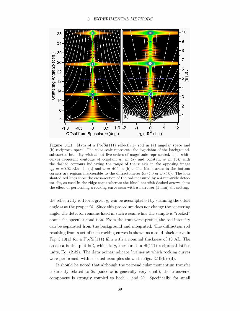
3. EXPERIMENTAL METHODS
Figure 3.11: Maps of a Pb/Si(111) reflectivity rod in (a) angular space and(b) reciprocal space. The color scale represents the logarithm of the background-subtracted intensity with about five orders of magnitude represented. The whitecurves represent contours of constant qx in (a) and constant ω in (b), withthe dashed contours indicating the range of the x axis in the opposing image[qx = ±0.02 r.l.u. in (a) and ω = ±1 in (b)]. The blank areas in the bottomcorners are regions inaccessible to the diffractometer (α < 0 or β < 0). The fourslanted red lines show the cross-section of the rod measured by a 4 mm-wide detec-tor slit, as used in the ridge scans whereas the blue lines with dashed arrows showthe effect of performing a rocking curve scan with a narrower (1 mm) slit setting.
the reflectivity rod for a given qz can be accomplished by scanning the offsetangle ω at the proper 2θ. Since this procedure does not change the scatteringangle, the detector remains fixed in such a scan while the sample is “rocked”about the specular condition. From the transverse profile, the rod intensitycan be separated from the background and integrated. The diffraction rodresulting from a set of such rocking curves is shown as a solid black curve inFig. 3.10(a) for a Pb/Si(111) film with a nominal thickness of 13 AL. Theabscissa is this plot is l, which is qz measured in Si(111) reciprocal latticeunits, Eq. (2.32). The data points indicate l values at which rocking curveswere performed, with selected examples shown in Figs. 3.10(b)–(d).
It should be noted that although the perpendicular momentum transferis directly related to 2θ (since ω is generally very small), the transversecomponent is strongly coupled to both ω and 2θ. Specifically, for small
69

3. EXPERIMENTAL METHODS
scattering angles qx ∝ ω 2θ. This fact results in a difference in the topologyof angular (ω-2θ) and reciprocal (qx-qz) space. Figure 3.11(a) shows theresults of the rocking curves used to determine the data in Fig. 3.10. Eachrocking curve is an ω scan for a specific value of 2θ and thus corresponds to asingle horizontal row in the image. In this manner, a map of the diffractionrod in angular space can be created. Since the width of the rod variesalong its length, rocking curves at different 2θ values require different stepsizes. To create an evenly spaced grid of points for the image, each rockingcurve was fit to an asymmetric Voigt curve (a convolution of a Gaussianand Lorentzian). To illustrate the different topology of angular space withrespect to reciprocal space, the white lines in the image show contours ofconstant qx, calculated using Eq. (3.7a). As can be seen, the width of the rodappears to follow the qx contours, which is especially noticeable as 2θ → 0,where the rod appears to flare out. The reason for this effect is that thediffraction rod is really a feature in reciprocal space, and as such will followits topology. This fact is explicitly demonstrated in Fig. 3.11(b), whichshows the same data as Fig. 3.11(a) but transformed into reciprocal space.The white lines in this case show contours of constant ω. In reciprocal space,the flaring-out effect is not present and the rod width is nearly uniformas a function of l.§ Since the rod is measured in angular space, it willappear to be broader at smaller scattering angles. Since scattering at α <
0 or β < 0 cannot be measured (blank areas in the bottom corners ofFig. 3.11), eventually the width of the rod in angular space is so large thatthe background cannot be accurately determined. This widening of the rodin angular space also has important ramifications for the ridge scan methoddiscussed in Sec. 3.6.2.
It is important to understand exactly what portion of reciprocal spaceis being measured by a rocking curve scan. The detector has a finite activearea defined by a pair of slits. This active area itself effectively integratesthe intensity over a 2D surface in reciprocal space. During the rocking curvescan, this surface is swept through reciprocal space to integrate over a 3Dvolume. The dimensions of this integration volume will determine the reso-lution of the rod measurement. This effect is illustrated in Fig. 3.12, whichshows a diagram representing the scattering geometry projected onto thescattering (xz) plane. For a given incident angle α, a range dβ of exitingbeams will be collected by the detector, corresponding to the angular ac-
§A slight broadening is evident at high values of l; however, this effect is due to theconvolution of the signal with the finite angular width of the slit used to measure therocking curves and is not due to actual broadening of the diffraction rod itself.
70

3. EXPERIMENTAL METHODS
q
dqz
dω ∼ dqx
kikf
βα
dβ
z
x
y
Figure 3.12: A diagram showing the range of momentum transfer collectedby the detector slits. For different β values, the orientation and length ofthe q vector is different, which collects a slightly diagonal slice of reciprocalspace that has a finite width in qz and effectively integrates over a range ofω (or qx).
ceptance of the slits. Each of these beams corresponds to a slightly differentq vector. The orientation of each q vector will be slightly offset from thesurface normal (z axis) by an amount dω = −dβ/2, which from Eq. (3.3a)corresponds to a variation
dqx = −k dβ sinβ (3.8)
in reciprocal space. Similarly, from Eq. (3.3b) the range of qz values whichare collected by the detector throughout the scan is
dqz = k dβ cosβ. (3.9)
The surface in reciprocal space over which the slits integrate is thus approxi-mately a rectangle that extends in the y direction (perpendicular to the pagein Fig. 3.12) due to the width of the slits normal to the scattering plane, andwhose other edge is a slanted line segment in the xz plane. The values ofdqx and dqz indicate the reciprocal space lengths between the endpoints ofthis line segment. Examples of the projection of this 2D rectangular surfaceonto the scattering plane (i.e., the line segment profile of the rectangle) areshown in Fig. 3.11 as red and blue lines. A rocking curve scan is thereforeequivalent to sweeping one of these rectangles across the diffraction rod inthe x direction, as shown with the blue dashed arrows. Such a scan willintegrate a slice of the rod that has a thickness of dqz. Since dqz ∝ cosβ,the thickness of this rod slice will vary as we move along the rod. This is
71

3. EXPERIMENTAL METHODS
the origin of the rod interception correction factor discussed in Sec. 2.5.4.In the case of 3D crystallography, where rocking curves are commonly
used to measure the integrated intensities of Bragg peaks, the detector slitsare opened relatively wide for the scan to maximize the integration volume.In that case, the Bragg peak is nominally a zero-dimensional feature (point)in reciprocal space. However, in surface diffraction, the features of interestare quasi-1D objects (rods), along which the intensity as a function of qz isdesired. In addition, the background surrounding these rods can be signifi-cant and must be taken into account. In this case, the preferred integrationvolume is a 2D cross-sectional slice of the rod that retains as much resolutionin qz as possible. As a result, the detector slits are generally narrowed tominimize dβ and hence dqz.
To summarize, the rocking curve method measures a cross-sectional pro-file of the diffraction rod for an approximately constant qz value. From thisprofile, the background can be found and the rod intensity integrated. Thismethod provides accurate rod intensities for a wide range of qz values. How-ever, since an individual scan must be carried out for each qz point alongthe rod, it requires a great deal of time both to collect the data and inits analysis. Since a high-demand synchrotron is generally used to do theexperiment, this limitation may be significant.
3.6.2 The Ridge Scan Method
As mentioned in the last section, the acceptance area of the detector itselfintegrates over a 2D surface in reciprocal space. If the diffraction rod issufficiently sharp in the transverse directions, a 2D cross-sectional slice of therod can be measured without rocking the sample at all by using sufficientlywide detector slit settings. In this manner, the integrated intensity of a pointon the rod is obtained directly with a single setting of the diffractometer.This type of measurement is illustrated in Fig. 3.11 with slanted red lines.This cross-section is truly a 2D slice of the rod, unlike the 3D volume thatis integrated with a rocking curve. In that case, the (narrower) slits werescanned across the diffraction rod, as shown with the blue lines and arrows.In the ridge scan method, a wider slit setting is used (hence the longer linein the figure) and the measurement is taken directly at each point along therod. Since the rod is integrated over a 2D surface instead of a 3D volume,the rod interception factor described in Sec. 2.5.4 is not needed.
The integrated intensity of the rod as a function of qz can thus be ob-tained by scanning α and β simultaneously while keeping α = β (ω = 0).
72

3. EXPERIMENTAL METHODS
This type of scan is commonly referred to as a θ-2θ scan, since both thescattering angle and the incident angle (which is equal to half the scatteringangle for the specular rod) are varied during the scan. This type of scan isequivalent to sweeping the slit profile shown at the bottom of Fig. 3.11(a)in a straight line up the middle of the map. The background level for eachpoint along the rod can be obtained by performing a similar type of scanwith an offset between α and β; i.e., with ω 6= 0. In this work, the back-ground for each ridge scan was obtained by taking the average of two scans,one with ω = 1 and another with ω = −1. Such background scans can bevisualized in Fig. 3.11(a) as sweeping up straight vertical lines in angularspace at the edges of the map. The results of using the ridge scan methodto measure the Pb/Si(111) specular rod in Fig. 3.11 is shown in Fig. 3.10as a red dotted curve. In both cases, the curves represent the backgroundsubtracted integrated intensity of the specular rod, with the experimentalcorrections described in Secs. 2.5.4 and 3.3.2 applied. Since the two meth-ods measure intensities on incompatible scales (the rocking curves integrateover a 3D volume of reciprocal space whereas the ridge scan integrates overa 2D surface), the ridge scan curve was multiplied by a scale factor to showthe two results on the same scale. The average of the two background scansthat were subtracted from the ridge scan is also shown in the figure as alight dotted blue curve.
The results from the two methods are essentially equivalent for l > 2.5.However, for the lower portion of the rod, the ridge scan method consistentlymeasures a lower intensity than the rocking curve method. The reason forthis discrepancy is that the size of the 2D surface used to integrate thetransverse profile of the diffraction rod is defined by the angular acceptanceof the detector slits. It is therefore a constant size in angular space. Thatis, the ridge scan samples a vertical swath of constant width in Fig. 3.11(a).However, as discussed in the last section, the diffraction rod appears tobroaden considerably in angular space as l → 0, following the contours ofconstant qx. At lower momentum transfers, the 2D integration surface isno longer wide enough in reciprocal space to sample the entire rod cross-section. This effect is illustrated in Figs. 3.10(b)–(d), where the angularrange sampled by the slits used to obtain the ridge scan data is shown withvertical dashed green lines. In Figs. 3.10(c) and (d), the range collected bythe slits clearly integrates over the full rod width whereas in Fig. 3.10(b),part of the rod intensity is not collected (note the different scale for ω).Therefore, the ridge scan method is only effective for obtaining integratedrod intensities for larger momentum transfers (in our case, for l > 2.5).
73

3. EXPERIMENTAL METHODS
Since this study focuses on the extended reflectivity, this limitation is notoverly restrictive.
Even though the ridge scan method is limited in the range of momentumtransfer that it can measure, it also possesses certain advantages over therocking curve method. First, since the diffraction rod is integrated over a 2Dsurface, the ridge scan method provides exceptionally high-resolution datain qz. In contrast, the rocking curve method always integrates a rod slice offinite thickness which limits its resolution in qz. More significantly though,the ridge scan method requires only a fraction of the amount of time toacquire a full set of extended reflectivity data compared to the rocking curvemethod. With the ridge scan method, the background-subtracted integratedintensity of the full rod can be measured with just three scans (one for ω = 0for the specular intensity and two background scans at ω = ±1), whereasa separate scan must be done for each point along the rod with the rockingcurve method. For example, the data in Fig. 3.10 represents the resultsof 280 individual rocking curves, each of which needed to be individuallyanalyzed to determine the background and to remove any spurious datapoints. Measuring the full diffraction rod using the rocking curve methodmay take 10–20 hours, depending on the spacing desired between the pointsalong the rod. In contrast, measuring the diffraction rod using the ridgescan method only takes about 20–40 minutes. For experiments such as thoseconducted in Chapters 5 and 6, where the specular rod of the same samplemay need to be measured dozens of times (at different temperatures orthicknesses), the ridge scan method is a necessity given the time constraintsof a synchrotron facility.
The ridge scan method provides a technique for measuring the upperportion of the reflectivity rod (the extended reflectivity) at high resolutionand in a short amount of time. For lower momentum transfers, the width ofthe diffraction rod must be measured to ensure that the detector slits in theridge scan collect the full integrated intensity of the rod. In practice, thiscan be verified by doing sample rocking curves to measure the transverserod profile. The angular width of the slits needed to integrate the entire rodwidth is then approximately twice the full width of the peak in the rockingcurve (dβ ≈ 2dω). In our case, it was found that with the slit setting used,the full rod intensity was collected for l > 2.5. For this reason, only datafor these momentum transfers were used in the experimental analyses.
74

3. EXPERIMENTAL METHODS
3.6.3 Error Analysis
Since the diffraction data were collected with a scintillation detector, whichproduces pulses that are counted, the statistical distribution of the raw in-tensity data should follow a Poisson distribution with a standard error of√
N0 where N0 is the number of pulses counted before background sub-traction and signal normalization. The fractional error in this case is thus1/√
N0. Since typical count rates were on the order of 104–105 c/s, thefractional errors due to statistical deviations were only about 0.3–1.0%. Toaccount for a certain degree of systematic error in the measurements (sam-ple misalignments, etc.), the statistical errors were combined quadraticallywith a 5% systematic error. Due to the high count rates, generally the bulkof the standard deviations for each data point are due to systematic errors.
In the process of doing the least-squares fits to the experimental data, areduced χ2 measure of the fit quality was used:
χ2 =1
N −MN∑
i=1
[yi − f(xi)]2
σ2i
(3.10)
where N is the number of points in the data set, M is the number of freeparameters in the model (thus, N −M is the number of degrees of freedom),yi = N0/Nm is the normalized count rate for data point i (Nm is the monitorcount discussed in Sec. 3.3.2), xi is its corresponding abscissa value, f(x)is the model function, and σi is the standard error for data point i. Asdescribed above, in our case the standard error is
σ2 =
(√N0
)2 + (0.05N0)2
N2m
, (3.11)
so
σ2i =
yi
Nm+ 0.025 y2
i . (3.12)
Thus, when χ2 ≈ 1 the model function describes the data to within theexperimental error of the measurements. Due to the multitude of differentfactors that influence the form of a reflectivity curve, typical χ2 values forthe best fits to the experimental data in Chapters 5 and 6 were generally inthe range χ2 = 5–10.
75

4 Free-Electron Models
4.1 Introduction
In an attempt to capture the essential physics of an ultrathin metal film, itis reasonable to approximate the system as a free-electron gas confined to aone-dimensional quantum well. This chapter develops a set of such modelsto describe some of the various thickness-dependent effects that arise dueto quantum confinement of a metal film’s itinerant electrons by its physicalboundaries (QSE) [83, 84]. The free-electron assumption in itself limits thedirect applicability of the unmodified models for the quantitative analysisof actual experiments. However, as will be seen, the addition of certain phe-nomenological factors can be done to mimic some of the physical realitiesof the system. The modified models are found to provide an adequate de-scription of the actual films studied, as long as they are interpreted withinthe proper context.
Adhering to the theme of simplicity, most of the models presented arebased upon a quantum well with infinite bounding potentials. Such a sim-plification enables us to derive analytic formulas for the wave functions ofthe confined electrons and the surface energy. The availability of an analyticsolution is conducive to incorporating the results of the model calculationinto a fitting algorithm with adjustable parameters that can be used to in-terpret experimental data. Since such a routine may need to recalculatethe model results thousands or even millions of times before arriving at anacceptable fit to the data, models that rely upon first-principles calculationsor that are purely numerical are not well-suited for incorporation into suchalgorithms due to their computationally intensive nature.
That being said, the finite quantum well model is explored at the end ofthe chapter for the sake of comparison. Conceptually it lacks the simplicityof the infinite well model. However, the finite well model offers an alternativeperspective within the free-electron framework. In the end, the results of thefinite well model are very similar to those found using the modified infinitewell model and as such offer a certain degree of validation that they areaccurate and physically reasonable.
76

4. FREE-ELECTRON MODELS
Before the specific models are presented, a certain theoretical base isdeveloped. First, in Sec. 4.2 the effects of quantum confinement on thecharge density inside an infinite well are described. Second, due to thediscrete quantum well states that arise, the Fermi level in a film is notnecessarily equal to that in the bulk material. This effect and differentviewpoints on how to approach it are discussed in Sec. 4.3, where it is foundthat the charge density oscillations of Sec. 4.2 provide valuable insight as tothe physical phenomena involved.
In the last two sections of the chapter, two different physical effects arediscussed in detail. The first is related to the Friedel-like oscillations inthe electronic charge density that arise at the film boundaries. Since theionic cores in the film’s crystalline lattice have a net positive charge, it isreasonable to expect them to respond to these electron density oscillations,causing lattice distortions with a corresponding periodicity. Two similarmodels are developed to describe these lattice distortions, which are usedin Chapter 5 to help explain the atomic-layer structure of thin Pb/Si(111)films.
The second effect is oscillations in the surface energy as a function ofthickness. These oscillations will be studied experimentally in Chapter 6,where it will be found that films annealed to a state of quasi-equilibrium havea wide distribution of thicknesses. The distributions are not smooth, though,indicating that some thicknesses are more stable than others, correspondingto variations in the surface energy of the film. In Sec. 4.5, a model for thiseffect within the free-electron context is presented, the functional results ofwhich are used in Chapter 6 to aid in the data analysis.
4.2 Charge Density
In the infinite well model, the free-electron wave function is subject to theboundary conditions
Ψ → 0 at z = 0, D (4.1)
where D is the width of the quantum well. The Fermi sphere of allowedelectronic states is correspondingly reduced to a series of subbands, as shownin Fig. 4.1, each having a wave function
Ψk(r) =
√2V
eikxx+ikyy sin(kzz) (4.2)
77

4. FREE-ELECTRON MODELS
kF
kz
n = 1
n = 2
n = 3
n = n0
ky
kx
Figure 4.1: Due to confinement of the itinerant electrons in the film toa quantum well, the Fermi sphere of allowed states is reduced to a set ofsubbands along the direction of confinement. The quantum number of thehighest occupied subband is denoted with n0.
where V is the volume of the system, the index kz can take on the values
kz =πn
Dn = 1, 2, 3, . . . , n0, (4.3)
and the quantum number of the highest occupied subband is
n0 = int(
kF D
π
). (4.4)
Thus, the wave functions for the electrons in each subband are that of a freeparticle in the xy plane (the plane of the film) and a standing wave in thez direction. The electronic charge density at a point in a free-electron gasis in general found by integrating over the Fermi sphere,
ρe(r) =2V
8π3
∫
|k|<kF
(−e)∣∣Ψk(r)
∣∣2d3k, (4.5)
where e is the magnitude of the charge of an electron and kF is the Fermiwave vector. However, in this case,
∣∣Ψk(r)∣∣2 = 2
V sin2(kzz), which is onlya function of z, as required by the translational symmetry of the system inthe xy plane. In addition, the Fermi sphere is no longer uniformly occupied,but is divided up into a series of discrete Fermi disks. Thus, the electronic
78

4. FREE-ELECTRON MODELS
charge density at a point 0 ≤ z ≤ D in the quantum well is
ρe(z) = − e
2π3
∫ kF
0dkz π
(k2
F − k2z
)sin2(kzz)
n0∑
n=1
2π
Dδ(kz − πn
D
)(4.6)
= − e
πD
n0∑
n=1
[k2
F −(πn
D
)2]
12
[1− cos
(2πnz
D
)]. (4.7)
The summation can be divided up into a portion which is constant withrespect to z and an oscillatory component:
ρe(z) = − e
2πD
[CD −
(k2
F +14
∂2
∂z2
)SD
(2πz
D
)](4.8)
where CD is given by
CD =n0∑
n=1
[k2
F −(πn
D
)2]
(4.9)
= n0k2F −
( π
D
)2 16n0(n0 + 1)(2n0 + 1), (4.10)
and SD is the dimensionless geometric sum
SD(x) =n0∑
n=1
cos(nx) (4.11)
=12
sin(n0x) cot(x
2
)− sin2
(n0x
2
). (4.12)
The subscripts on SD and CD are a reminder that both of these quantitieswill change with the size of the quantum well. The oscillatory behavior of ρe
is thus captured in SD, which gives rise to a n0-slit interference pattern witha characteristic wavelength of D/n0 ≈ π/kF = λF /2 (one half of the Fermiwavelength). To focus on the oscillatory component, the self-normalizedcharge density variations may be considered:
δρ(z) ≡ ρe(z)− 〈ρe(z)〉〈ρe(z)〉 (4.13)
= − 1CD
(k2
F +14
∂2
∂z2
)SD
(2πz
D
)(4.14)
where 〈· · · 〉 indicates the average over z. An example of this quantity isshown in Fig. 4.2 as a solid curve, where it exhibits sinusoidal oscillationsthat dampen away from the film boundaries (vertical dashed lines).
Note that in the limit D → ∞, our system changes from a quasi-two-
79

4. FREE-ELECTRON MODELS
-1
0
543210 ( F)
bulk
Figure 4.2: The self-normalized charge density variations in a metal film(solid curve) exhibit strong oscillations with a wavelength of λF /2, whichdampen away from the film boundaries. In the bulk limit (red dotted curve),they are identical to the normal Friedel oscillations found near the surfaceof bulk metals.
dimensional film into a semi-infinite slab. In this limit,
SD(x) →∫ kF
0cos
(kzDx
π
)D
πdkz (4.15)
=1x
sin(
kF Dx
π
)(4.16)
CD →∫ kF
0
(k2
F − k2z
) D
πdkz (4.17)
=D
π
23k3
F (4.18)
and Eq. (4.14) becomes
limD→∞
δρ(z) = −(
43k3
F
)−1 (k2
F +14
∂2
∂z2
)1z
sin(2kF z) (4.19)
= −32
(1 +
∂2
∂u2
)sinu
u(4.20)
= 3(
cosu
u2− sinu
u3
)(4.21)
where the substitution u = 2kF z has been made. This equation is thefamiliar form of the Friedel oscillations in the electron density near thesurface of a bulk metal, which one would expect to recover in this limit.For comparison, these regular Friedel oscillations are shown in Fig. 4.2 fora semi-infinite bulk metal (dotted curve).
When D is sufficiently large, the charge density variations are well rep-
80

4. FREE-ELECTRON MODELS
resented by the superposition of the Friedel oscillations due to the two filmboundaries. Intuitively, the Friedel oscillations derived from the two bound-aries can overlap and interfere as D becomes small, but the situation is ac-tually more complicated. The Friedel oscillations in a bulk metal arise dueto the upper limit to the wave vector (the Fermi level) of electronic statesavailable as Fourier components and the pinning of their relative phases dueto the loss of translational symmetry. The states that are available, though,form a continuum from k = 0 to kF . In the case of a thin film, the electronwave functions are pinned in phase by both boundaries, giving rise to inter-ference effects. Furthermore, the continuum of k states is reduced to a setof subbands, as shown in Fig. 4.1. This reduction in the Fourier basis setcan also lead to differences from the bulk. In short, charge oscillations inρe(z) and δρ(z) for a film are the result of a phased sum of a discrete set ofsubband wave functions. One distinct difference between the film’s densityoscillations and the bulk Friedel oscillations is that the charge density vari-ations in the film do not oscillate about the average charge density of thefilm (which would correspond to δρ = 0), but a value slightly larger. Thiseffect will have important consequences for the Fermi level.
4.3 Fermi Level
As the size of the quantum well gets smaller, the separation between thesubbands will get wider and the number of available states will decrease.There are two consequences of this that need to be recognized. First, thenumber of occupied electronic states (i.e., the total number of electrons)in the quantum well will not necessarily be proportional to the film thick-ness if one assumes a fixed Fermi level. Second, as can be seen in Fig. 4.2,the charge density variations have tails at the film boundaries. As a re-sult, regions of electron depletion are present near the film boundaries. Tocompensate, a net charge builds up in the rest of the film, which producesa charge imbalance. Both of these effects can be compensated for by anappropriate adjustment of the Fermi level as a function of thickness and byletting the quantum well width expand slightly at the film boundaries sothat the electron density can tunnel slightly past the classical boundaries ofthe film. Specifically, there are two different constraints that can be appliedto the model:
Constraint #1: Charge neutrality. The number of electrons in the the-oretical quantum well is required to be equal to the number of electrons oneexpects to find in the film given the bulk electron density of the material.
81

4. FREE-ELECTRON MODELS
This constrains the film to be electrically neutral overall, which is appro-priate for free-standing slab calculations, but not necessarily for supportedfilms, where an interface charge layer can form.
Constraint #2: Charge balance. The average electronic charge densityin the middle of the quantum well is balanced with the constant positivebackground due to the ion cores; i.e., the total charge density oscillatesabout zero. This constraint minimizes the net electric field in the film andhence also its Coulomb energy.
Although similar, these two constraints are distinct from each other —charge neutrality (Constraint #1) is not necessarily equivalent to chargebalance (Constraint #2). In the bulk, there is no distinction since bound-ary effects are negligible, but in the case of a film, both constraints aresatisfied only under very special circumstances, as will be seen below.
In the simplest case, the width of the quantum well is D = Nt, where t
is the average interlayer spacing of the film. This width is also the extent ofthe positive uniform background in the jellium model and will be referred toas the classical width of the film since it ignores any boundary effects and isappropriate in the D →∞ limit. However, in this case the infinite boundarypotentials do not allow any of the electronic charge density to spill past theclassical boundaries of the film. Nonetheless, such a scheme represents areasonable starting point for discussion. A more realistic treatment of theboundary conditions will be introduced later.
To enforce charge neutrality (Constraint #1), the diminishing numberof occupied states for decreasing film thickness must be compensated by anappropriate adjustment of the Fermi level. Given the thickness, the totalnumber of electrons in the film is
Ne = NvalNA
Acell(4.22)
where N is the number of atomic layers in the film, A is the surface area ofone film interface, Nval is the number of itinerant valence electrons per atomof film material (Nval = 4 for Pb), and Acell is the area of the surface unitcell. In contrast, the total number of electrons in the theoretical quantum
82

4. FREE-ELECTRON MODELS
2.0
1.8
1.6
1.4
1.2
1.0
Nor
mal
ized
76543210Pb Layers
Infinite Well Finite Well Infinite Well + ∆
Figure 4.3: The Fermi energy of a Pb(111) film as a function of thickness,normalized to its bulk free-electron value. In the infinite well model, whenthe quantum well width is exactly equal to Nt, the Fermi level rises dras-tically as the film thickness decreases (dotted curve) to compensate for theareas of electron depletion near the film boundaries (see Fig. 4.4). However,if the electron density is allowed to spill past the classical film boundaries,such compensation is unnecessary and the Fermi level oscillates about itsbulk value (solid curve). This Fermi level is very similar to that found in amodel where the bounding potentials are finite (dashed curve).
well is calculated by summing over the allowed subbands
NQWe =
2V
8π3
∫
|k|<kF
d3kn0∑
n=1
2π
Dδ(kz − πn
D
)(4.23)
=V
2π2D
n0∑
n=1
π
[k2
F −(πn
D
)2]
(4.24)
=A
2πCD (4.25)
where CD is defined in Eq. (4.10). Setting NQWe = Ne yields the constraint
CD =2πNvalN
Acell. (4.26)
The results of solving this constraint for the Fermi energy, EF = ~2k2F
2me, are
shown in Fig. 4.3 (dotted curve) normalized to the bulk free-electron value.As D → 0 the Fermi energy rises steeply and for the first few integer N thick-nesses, the Fermi level is up to ∼40% larger than its bulk value. Cusps arealso evident at thicknesses where an additional subband becomes occupied
83

4. FREE-ELECTRON MODELS
4
0
4
0
(a)
(b)
∆
|
e| (
e/at
om)
Figure 4.4: Charge density profiles for a quantum well with N = 5. (a)Assuming the boundary potentials are infinite in magnitude, the electroniccharge density is forced to zero at the film boundaries, causing an area ofelectron depletion (shaded areas below |ρe| = 4, the background chargedensity from the Pb ion cores). To compensate, the inner portion of thefilm takes on a net charge. (b) If the charge density is allowed to spill pastthe classical boundaries of the film, as happens in a real film, this effect canbe minimized.
(i.e., when n0 increases discontinuously) as the film thickness increases.The steep rise in EF is specific to the infinite boundary potentials, since it
is not present in a finite well model (dashed curve in Fig. 4.3, see Sec. 4.5.3).The infinite boundary potentials force the wave functions of all the quan-tum well states to go to zero, creating an area of electron depletion near thefilm boundaries, as illustrated in Fig. 4.4(a) with electron density profilesas calculated in Sec. 4.2. In order to satisfy the condition of overall chargeneutrality, Eq. (4.26), the electron density in the center portion of the quan-tum well must get ever larger with respect to the positive background asthe film thickness decreases to compensate for these areas of electron de-pletion. This charge imbalance leads to a net electric field inside the metalfilm. However, in a real metal film the confining potentials are not infiniteand the electron density will spill slightly past the classical boundaries of
84

4. FREE-ELECTRON MODELS
the film, reducing the region of electron depletion. To simulate this aspectof the system, define the well width to be
D = Nt + 2∆ (4.27)
where ∆ is the distance the quantum well is allowed to expand at eachboundary to allow for some charge spillage. This procedure is analogous tothe boundary phase shifts that are often employed in quantum well analyses[36]. For now, the symmetric case will be considered where the chargespillage at each interface is the same, which is not the case for an actualsupported film.
The charge imbalance that results in the steep rise in EF is minimizedwhen the electronic charge density oscillates about the constant positivebackground level due to the ionic cores; i.e., when Constraint #2 is satisfied.This condition is obtained by extracting the non-oscillatory component ofEq. (4.8)
ρe = − e
2πD
(CD +
12k2
F
). (4.28)
Note that this quantity is distinct from the average electronic charge density,〈ρe(z)〉, which is equal to the first term only — the quantity SD has a zerointegral between z = 0 and D, but oscillates about the value −1
2 away fromthe boundaries, as can be seen from Eq. (4.12). This difference results fromthe charge spillage tails in ρe(z) at the film boundaries, as seen in Fig. 4.4.In the limit D →∞, the effects of the interfaces become negligible, CD ∝ D
and ρe → 〈ρe(z)〉. This discrepancy is also evident in Fig. 4.2, where theself-normalized charge density variations for the film can be seen to oscillateabout a value slightly larger than zero. The condition of charge balance isthus obtained when ρe is equal to the magnitude of the constant positive(jellium) background
ρe = −Nval e
Acellt, (4.29)
which when combined with Eq. (4.28) yields
CD =2πNvalD
Acellt− 1
2k2
F . (4.30)
This constraint is very similar in form to Eq. (4.26). Note that if D = Nt,both constraints are only satisfied in the limit N → ∞. However, withD 6= Nt there are two degrees of freedom that can be used to meet thesetwo constraints: kF and ∆.
85

4. FREE-ELECTRON MODELS
1.12
1.08
1.04
1.00
0.96
Nor
mal
ized
87654321Well Thickness (AL)
Figure 4.5: The Fermi energy for a Pb(111) film as a function of thicknessapplying only the condition of charge balance (Constraint #2) inside thefilm, normalized to the free-electron bulk value.
Solving Eqs. (4.26) and (4.30) simultaneously along with Eq. (4.27), onefinds that the charge spillage is proportional to the Fermi energy
∆ =Acellt
4πNval
m
~2EF . (4.31)
Using the bulk Fermi level for Pb(111) gives a charge spillage of ∆ = 0.262t.The Fermi level for the infinite well model with this charge spillage is shownin Fig. 4.3 as a solid curve, which is within 1% of its bulk value for integerN ≥ 1. Figure 4.4(b) shows the electronic charge density profile inside thequantum well in this case, where it can be seen that the tails in the density liepartially outside the classical boundaries defined by the positive background,thus reducing the region of electron depletion within the classical boundaries.The result is a surface dipole layer. Note that the issue of charge spillageis automatically accounted for in a model with finite bounding potentials.Such a model is developed in Sec. 4.5.3, which yields results very similar tothe present model, as shown in Fig. 4.3 with a dashed curve.
It is also possible to enforce the charge balance condition (Constraint#2) while relaxing the charge neutrality constraint (Constraint #1). In thiscase, since Eq. (4.30) only explicitly contains the variables D and kF [asopposed to Eq. (4.26), which also explicitly depends on N ], the Fermi levelcan be found for a given well thickness. Solving Eq. (4.30) for kF in thiscase results in the Fermi level shown in Fig. 4.5. Note that here the Fermilevel is only dependent on the width of the quantum well, which is distinctfrom the values shown in Fig. 4.3, which are determined by N , the numberof atomic layers in the film. Of course, if the charge neutrality constraint
86

4. FREE-ELECTRON MODELS
is relaxed, then the theoretical film can take on a net charge. However,in practice the charge spillage parameter is still used, only it is utilizedas an adjustable parameter. As long as it is close to the value given byEq. (4.31), the discrepancy between total charge of the film and that of thequantum well is small. For a film supported on a substrate and in contactwith a reservoir of electrons, this effect is accounted for by the formation ofan interface charge layer. For such a system, charge conservation must beconsidered for the entire system, not for the film alone.
In summary, if only Constraint #1 is enforced, without taking into ac-count the charge spillage of the electron density past the classical boundariesof the film, the Fermi level rises steeply for small film thicknesses, a situationthat does not reflect reality. When charge spillage is added to the modeland charge balance is approximately achieved, the Fermi level is very closeto its bulk value. In this case, Constraint #1 is enforced while Constraint#2 is only approximately obeyed. Alternatively, in some instances it maybe more appropriate to enforce the charge balance condition while relaxingthe condition of charge neutrality. In this case, Constraint #2 is enforcedstrictly and the Fermi level is close to the bulk value as shown in Fig. 4.5.Constraint #1 will be approximately satisfied as long as the charge spillageis a reasonable value. In this case, the film takes on a net total charge; how-ever, such an effect is justified if the experimental reality of the substrate istaken into account.
4.4 Lattice Distortions
4.4.1 Overview
In Chapter 5, an analysis of x-ray diffraction data is presented that indicatesthe presence of significant lattice distortions (strain) in the atomic-layerstructure of ultrathin Pb/Si(111) films. These distortions are then correlatedwith the free-electron charge density oscillations described in Sec. 4.2. Inthis section, the free-electron models used in the experimental analysis arederived. In principle, the models are valid for any sufficiently free-electron-like metal film; however, the discussion and examples will concentrate onthe effects specific to Pb films since they are most applicable to the presentwork.
To relate the lattice distortions to the charge density variations, thereare two models that can be followed. Either one can recognize that anylattice distortions due to variations in the charge density will be propor-
87

4. FREE-ELECTRON MODELS
tional to the local gradient of the charge density near each atomic plane,or one can calculate the electrostatic force on each atomic plane due to thecharge distribution of the entire system. Within the local gradient approx-imation, the positively charged atomic cores move toward regions of higherelectronic charge, but the charge distribution away from the point of inter-est is ignored. The two models actually yield very similar functional formsfor the electronic forces, which is to be expected. The electrostatic fieldcorresponds to an integral of the charge density, while the local gradientcorresponds to a derivative of the charge density. Since the charge den-sity variations within the film are dominated by sinusoidal oscillations (at awavelength of λF /2), its integral and derivative should be similar. Numer-ical results to be presented below confirm that the differences (with properchoices of normalization constants) are small and well within the errors ofour analysis.
In Sec. 4.3 it was noted that the electronic charge density will tunnel intothe classically forbidden regions slightly and accounted for this reality withsymmetric charge spillage parameters at the well boundaries. However, forthe purpose of describing lattice distortions in the film, the asymmetry inthe properties of the two film interfaces is important. Thus, in this sectionthe width of the quantum well is defined to be
D = ∆s + Nt + ∆0 (4.32)
where ∆s and ∆0 are the charge spillage distances into the substrate andvacuum, respectively. Given this definition, the coordinate positions of eachatomic plane in the absence of any lattice distortions would be
zj = ∆s + (j − 12)t j = 1, 2, . . . , N, (4.33)
where j = 1 corresponds to the atomic layer closest to the substrate. Theintroduction of independent charge spillage parameters into the model isessentially equivalent to introducing one phase shift function at the surfacez = D − ∆0, and another at the buried interface z = ∆s. For an infinitebarrier, the phase shift has a fixed value of −π, but by moving the filmboundaries by ∆s and ∆0, the phase shifts become adjustable and can bemade to mimic the actual system [36].
The presence of the substrate is therefore being taken into account ex-plicitly in these models. Thus, the application of Constraint #2 is moreappropriate in this case and the Fermi level shown in Fig. 4.5 will be used.Charge is conserved for the film-substrate system but not necessarily for the
88

4. FREE-ELECTRON MODELS
-1
0
1 (Å
-1)
7654321Pb Layer
-5
0
5
(
) (V
/Å)
4
3
2
1
0|
(
)| (
e/at
om)
(a)
(b)
Figure 4.6: (a) The electronic charge density (solid curve) with a posi-tive uniform background (dotted lines) for a Pb(111) film with a nominalthickness of 7 AL. (b) The electric field inside the quantum well (solidcurve) compared to the first derivative of the self-normalized charge den-sity variations (dotted curve). Vertical dotted lines indicate the positions ofatomic planes in the well where the functions are sampled. The two curvesare functionally similar at the atomic planes but differ in the boundaryregions.
film alone; thus, the condition of charge neutrality for the film (Constraint#1) is not necessarily strictly obeyed. Since the values for ∆0 and ∆s wereboth found to be close to the value given by Eq. (4.31), the magnitude ofthe interface charge layer will be small and well within reasonable expecta-tions (a fraction of e per interface atom is typical, depending on the chargetransfer [85]).
4.4.2 The Local Charge Density Gradient
In calculating the local gradient of the charge density, any uniform posi-tive background (as in the jellium model) can be ignored since it does notcontribute to the derivative of the charge density anywhere except the twodiscontinuities at the film boundaries. Similarly, the constant portion tothe electronic charge density, CD, does not contribute to the charge densitygradient. Thus, for simplicity the self-normalized charge density variations,
89
4. FREE-ELECTRON MODELS
Eq. (4.14), are considered. Under the assumption that the displacementof each atomic plane is proportional to the local gradient of the calculatedcharge density, the change in atomic layer spacing between layers j and j+1is
∆tj,j+1 = K
[∂
∂zδρ(zj+1)− ∂
∂zδρ(zj)
](4.34)
where a linear response coefficient K has been included. Since this quantityinvolves a local difference, the local gradient approximation is expected towork well. In other words, electrostatic fields derived from charges far awayfrom the two atomic layers of interest should have little effect. This methodof calculating the lattice distortions results in a model with four adjustableparameters: K, ∆s, ∆0, and t. The last quantity should be close but notnecessarily identical to the value found in the bulk material.
An example of the charge density inside the quantum well in this model isshown in Fig. 4.6(a) (solid curve) along with its first derivative in Fig. 4.6(b)(dotted curve with scale on the right axis). Since the displacement of eachatomic plane in this model follows the first derivative of the charge densityvariations, this is the quantity that will determine the form of the latticedistortions. Since it is the derivative of an oscillatory function with a pe-riodicity of λF /2, the lattice distortions will also have this periodicity. ForPb(111), λF /2 ≈ 2
3 AL and so every two interlayer spacings of the film willcorrespond to approximately three full oscillations in the derivative of δρ.Since the lattice consists of discrete atomic planes, any distortions due tothe electronic charge density variations are therefore expected to have anapproximately bilayer periodicity.
Note that our numbering convention for the atomic layers differs fromthat used in many other studies in the literature, where the notation d12 isoften used to denote the interlayer distance between the two layers closestto the vacuum. Hence,
d12 = ∆tN−1,N + t
d23 = ∆tN−2,N−1 + t
...
dN−1,N = ∆t1,2 + t.
4.4.3 The Electrostatic Force
To calculate the electrostatic force, the total charge density is needed, in-cluding contributions from the positive atomic cores. In keeping with the
90
4. FREE-ELECTRON MODELS
spirit of the free-electron model, a uniform positive (jellium) background isused. The total charge density is then
ρ(z) = ρe(z) +Nval e
Acell t
[H(z −∆s)−H(z −D + ∆0)
], (4.35)
where H(x) is the Heaviside step function
H(x) =
0 x < 0
1 x > 0.(4.36)
The electric field is related to the charge density by
∂
∂zE(z) =
1ε0
ρ(z) (4.37)
where E is the z component of the electric field (the only non-zero componentby symmetry). Integrating this equation and using Eqs. (4.8) and (4.35)yields
E(z) =1ε0
∫ z
0ρ(z′)dz′ + E(0)
= − e
2πε0D
[CDz −
n0∑
n=1
(Dk2
F
2πn− πn
2D
)sin
(2πnz
D
)]
+Nval e
Acell t
[R(z −∆s)−R(z −D + ∆0)
]+ E(0) (4.38)
for the electric field, where R(x) is the ramp function
R(x) =
0 x < 0
x x > 0.(4.39)
The atomic cores each have a net charge of Nvale so the change in theinterlayer spacing between layers j and j + 1 is
∆tj,j+1 =Nval e
K ′[E(zj+1)− E(zj)
](4.40)
where K ′ is a force constant. Note that the term E(0) in Eq. (4.38) has noeffect on the interlayer spacings.
The electric field model for the lattice distortions also has four adjustableparameters, as with that of the last section, with the role of the linearresponse coefficient K taken by 1/K ′. A comparison of the electric field tothe first derivative of the charge density variations is shown in Fig. 4.6(b). As
91

4. FREE-ELECTRON MODELS
would be expected, they have a similar functional form over the range whereatomic planes are located. The differences can become significant outsidethe atomic layers due to the tail of charge spillage, but these differences areirrelevant to our analysis of atomic layer strain.
4.5 Surface Energy
4.5.1 Overview
In Chapter 6 a stability analysis is presented of Pb/Si(111) films that havebeen annealed to a state of quasi-equilibrium. Such experiments provideinformation on the relative stability of different film thicknesses over a widerange of thicknesses. In this section, two different free-electron models forthe surface energy of a metal film are discussed. The first model is basedupon an infinite quantum well model like that of the previous sections of thechapter, whereas the second model is based upon a quantum well with finitebounding potentials, the results of which are compared with the infinite wellmodel and are found to be similar.
These models are meant only to illustrate some of the thickness-depen-dent effects due to confinement of the itinerant electrons in a metal film(QSEs) and are not meant to describe the surface energy in quantitativedetail. Hence, only the functional form of the surface energy will be used inthe experimental analysis, with adjustable parameters included to accountfor the specific phenomenology encountered in the actual experiment. Forsimplicity, only the symmetric case is considered where the charge spillageat each interface is the same; i.e., the calculation is for a free-standing slab.Thus, the Fermi level shown in Fig. 4.3 as a solid curve is used where bothconstraints are approximately obeyed by using the charge spillage given byEq. (4.31) for the bulk free-electron Fermi energy. Since this calculationdoes not take into account the differences in the two film boundaries (i.e.,no substrate), it should only be considered correct to within an unknownphase shift with respect to the interface (that will henceforth become anadjustable parameter).
4.5.2 Infinite Well
The point of departure for calculating the surface energy of a metal film isthe same as it was in Sec. 4.2; namely, the film is modelled by a free-electrongas confined to a quantum well with infinite potential barriers. In general,
92

4. FREE-ELECTRON MODELS
the energy of a free-electron gas is
E =2V
8π3
∫
|k|<kF
d3k~2|k|22me
. (4.41)
However, when the gas is confined to a quantum well, the Fermi sphere ofallowed states is reduced to a series of subbands, as shown in Fig. 4.1. Thetotal electronic energy of the film then becomes
E =2V
8π3
∫
|k|<kF
d3k~2|k|22me
n0∑
n=1
2π
Dδ(kz − nπ
D
)(4.42)
=A~2
4π2me
n0∑
n=1
∫ √k2
F−k2z
02πk‖
(k2‖ + k2
z
)dk‖ (4.43)
=A~2
8πme
n0∑
n=1
(k4
F − k4z
)(4.44)
where A is the surface area of one interface of the film such that V = DA.In the last two expressions it is implicit that kz is the discrete index givenby Eq. (4.3). Substituting the explicit values for kz into the formula yields
E =A~2
8πme
[n0k
4F −
( π
D
)4n0∑
n=1
n4
](4.45)
=A~2
8πme
[n0k
4F −
( π
D
)4 130
n0(n0 + 1)(2n0 + 1)(3n20 + 3n0 − 1)
]. (4.46)
The total energy can be separated into contributions from the bulk andsurface [71]
E = εbV + 2εsA, (4.47)
where εb and εs are the bulk and surface energy densities, respectively. Thefactor of two results from the two separate surfaces of our model systemslab. The bulk contribution can be found by taking the D → ∞ limit ofEq. (4.46), when boundary effects are negligible,
εb = limD→∞
E
V(4.48)
=~2
(kbulk
F
)5
10π2m(4.49)
=35
Ne
VEbulk
F , (4.50)
93

4. FREE-ELECTRON MODELS
where the free-electron results for the electron density NeV = 1
3π2
(kbulk
F
)3
and the bulk Fermi energy EbulkF =
~2(kbulkF )2
2mewere used to arrive at the last
expression, which may be more familiar to the reader. Note that this sameexpression can be obtained by integrating Eq. (4.41) without the quantiza-tion condition, Eq. (4.3). Using Eqs. (4.46) and (4.47), the surface energydensity is then
εs =~2
16πm
[n0k
4F −
45π
(kbulk
F
)5D
−( π
D
)4(
15n5
0 +12n4
0 +13n3
0 −130
n0
)]. (4.51)
Using the Fermi level as found in Sec. 4.3 (solid curve in Fig. 4.3), therelative surface energy per surface atom, ES = Acellεs, for a Pb(111) filmcalculated with Eq. (4.51) is shown in Fig. 4.7(a) as a continuous functionof N (solid curve). A constant offset, which is irrelevant in a discussion ofthe relative stability of different thicknesses, has been subtracted off so thatthe amplitude of the oscillations is more apparent. The oscillations havea wavelength of π/kF = λF /2. This behavior, which is characteristic ofquantum size effect phenomena, can be understood as follows. The numberof subbands, or Fermi disks (see Fig. 4.1), that falls below the Fermi levelis n0 = int
(kF D
π
), so every expansion of the well D → D + π/kF results
in an additional subband crossing the Fermi level. This periodic additionof subbands results in oscillations in the surface energy that dampen as thesubbands get closer together with increasing film thickness. Since the Fermilevel shown in Fig. 4.3 is relatively constant, the oscillations in the surfaceenergy have a regular periodicity of π/kF .
Since the film must be composed of an integer number of atomic layers,the surface energy of an actual film will only take on the values at integerN , which are shown in Fig. 4.7(b) as open circles. Even-odd alternations inthe values are evident with a phase reversal (even-odd crossover) occurringperiodically. This effect is due to interaction of the discrete nature of theatomic lattice structure of the film with the oscillations in the surface energy.Half the Fermi wavelength for Pb(111) is very close to 2
3 an atomic interlayerspacing; thus, every two film layers corresponds to approximately three fulloscillations in the surface energy. Since the relationship is not exact, thebilayer alternations will have a beating pattern superimposed over themcausing the phase reversal effect. The envelope of this beating function isshown in Fig. 4.7(b) with dashed curves.
94

4. FREE-ELECTRON MODELS
-50
-25
0
25
50 Theory Fit
-20
-10
0
10
20
191715131197531Pb Thickness
(AL)
Theory Fit
(m
eV)
(a)
(b)
Figure 4.7: (a) The surface energy for a Pb(111) film calculated usinga model based on a free-electron gas confined to an infinite quantum wellwith charge spillage (solid curve). Oscillations are evident that are well-described by a damped sinusoidal form (dotted curve). (b) The same datafor thicknesses of an integer number of atomic layers. Bilayer oscillationswithin an overlying beating pattern (the envelope for which is shown withdashed curves) result from interference of the oscillations shown in (a) andthe discrete lattice of the crystalline film.
The relative surface energy is well-described by the phenomenologicalsinusoidal form
ES = Asin(2kbulk
F Nt + φ)Nα
+ B (4.52)
where A is an amplitude parameter, φ is a phase shift factor that will bedependent on the interface properties of the film, α is a decay exponent, andB is a constant offset, which was subtracted off from ES to obtain the valuesin Fig. 4.7. A fit of this function to the surface energy is shown as a dottedcurve in Fig. 4.7(a) and as crosses in Fig. 4.7(b). The decay exponent, whichis the only parameter value used in the experimental analysis, was found tobe α = 1.77 ± 0.09 over the range of N relevant to this work (it can vary
95

4. FREE-ELECTRON MODELS
z0 D
ESi Pb Vacuum
n = 1
n = 2
n = 3
n = 10EF
0
Vs
V0
Φ0
Φs
Figure 4.8: A schematic of the finite quantum well used to calculate thesurface energy. Two potential barriers confine the quantum well states tothe Pb film in the middle of the diagram. The wave functions are shownfor n = 1, 2, 3, and 10.
slightly for different ranges of N).
4.5.3 Finite Well
An alternative model for the surface energy of a thin metal film can beconstructed with finite potential barriers. The quantum well for such amodel is shown schematically in Fig. 4.8, where Vs is the confining potentialat the buried interface, and V0 is the vacuum confinement potential. Thesepotentials can be broken up into the components
Vs = EF + Φs
V0 = EF + Φ0
(4.53)
96

4. FREE-ELECTRON MODELS
where Φ0 is the work function of the film material and Φs is an effectivepotential step encountered by an electron travelling between the film andsubstrate. In an actual physical system, the electrons in the film materialare confined by the band gap of the semiconductor substrate, which doesnot behave like a simple potential barrier [36]. Thus, a simple step-potentialmodel is not expected to accurately describe the system. Nonetheless, thefinite quantum well model provides an alternative to the infinite well andillustrates some of the general strengths and weaknesses of using a free-electron model. In all subsequent calculations, the values Φ0 = 4 eV, thework function of Pb, and Φs = 0.6 eV, the Schottky barrier of the Pb/Si(111)interface [85], will be used.
The z components of the wave functions for the confined states in thismodel are of the form
ψ(z) =
C1 exp (κsz) z < 0
C2 sin(kzz) + C3 cos(kzz) 0 < z < D
C4 exp [−κ0(z −D)] z > D
(4.54)
where C1–C4 are constants subject to normalization and boundary condi-tions, and κs, κ0, and kz are all real quantities for confined states. Enforcingenergy conservation at the well boundaries (i.e., the three regions of the wavefunction must have the same energy) leads to the two relations
κs =
√2mVs
~2− k2
z
κ0 =
√2mV0
~2− k2
z .
(4.55)
Requiring continuity of ψ and its first derivative at the boundaries z = 0and z = D results in four more conditions
C1 = C3
C1κs = C2kz
C4 = C2 sin(kzD) + C3 cos(kzD)
−C4κ0 = C2kz cos(kzD)− C3kz sin(kzD),
(4.56)
which can be solved algebraically to yield the transcendental equation
tan(kzD) =κs + κ0
k2z − κsκ0
kz. (4.57)
Due to the periodic nature of the tangent function on the left side of this
97

4. FREE-ELECTRON MODELS
equation, there will be a series of discrete solutions to this equation for kz
(and thus also κs and κ0) corresponding to the discrete subbands or Fermidisks shown in Fig. 4.1. Using the trigonometric identities
arctan(
x + y
1− xy
)= arctanx + arctan y
and
arctanx =π
2− arctan
(1x
),
yeilds the result
kzD = nπ − arctan(
kz
κs
)− arctan
(kz
κ0
), (4.58)
which can be solved numerically for the discrete solutions indexed by theinteger n, which is the quantum number of the corresponding subband.Note that in the limit Vs, V0 → ∞, this equation reduces to Eq. (4.3), thequantization condition for the infinite well. Equation (4.58) is the usualBohr-Sommerfeld quantization rule, with the two arctangent terms relatedto the phase shifts at the two boundaries.
Finally, if one wishes to fully solve for the wave function given inEq. (4.54), the values for the constants C1–C4 can be determined by solvingthe normalization condition
∫ ∞
−∞
∣∣ψ(z)∣∣2dz = 1, (4.59)
which yields
C12
2κs+
C42
2κ0+
D
2(C2
2 + C32)
+1
4kz
(C3
2 − C22)sin(2kzD)
+C2C3
2kz
[1− cos(2kzD)
]= 1. (4.60)
Sample wave functions are shown in Fig. 4.8 for different subbands.As in Sec. 4.3, the Fermi level must be appropriately chosen so that the
number of electrons in the quantum well,
NQWe =
A
2π
∑
kz<kF
(k2
F − k2z
), (4.61)
remains equal to the number of free electrons given the amount of film
98

4. FREE-ELECTRON MODELS
20
10
0
-10
191715131197531Pb Thickness
(AL)
Theory Fit
-50
-25
0
25
50 Theory Fit
(m
eV) (a)
(b)
Figure 4.9: (a) The surface energy for a Pb(111) film calculated using amodel based on a free-electron gas confined to a finite quantum well (solidcurve), along with a fit to a damped sinusoidal function (dotted curve). (b)The same data for integer numbers of atomic layers. Bilayer oscillationssimilar to those in Fig. 4.7(b) are evident with a slightly different envelopefunction.
material, Eq. (4.22). The resulting Fermi level for a Pb(111) film is shown inFig. 4.3 as a dashed curve, which is very similar to that found in the infinitewell model with charge spillage. In this case, the Fermi energy remainsabove the bulk value for all thicknesses, though, with its value about 4%larger than the bulk for N = 1 and much closer thereafter.
A completely analogous procedure can be used to reach Eq. (4.44) forthe total electronic energy of the film and
εs =~2
16πm
∑
kz<kF
(k4
F − k4z
)− 45π
(kbulk
F
)5D
(4.62)
for the surface energy density. The relative surface energy per surface atom
99

4. FREE-ELECTRON MODELS
4
0
| (e
/ato
m)
Figure 4.10: The electronic charge density inside the film calculated withthe finite well model. The profile is very similar to that from the infinitewell model with charge spillage, Fig. 4.4(b). However, the average densityinside the film does not exactly cancel with the positive ionic background,resulting in the upwards bend in the surface energy as N → 0.
is shown in Fig. 4.9(a) with the values for integer N shown in Fig. 4.9(b). Itexhibits oscillations similar to those seen with the infinite well in Fig. 4.7. Inaddition, a slight upwards bend to the surface energy is apparent as N → 0,which is particularly noticeable in the integer N data of Fig. 4.9(b). Thiseffect can be accounted for by adding an additional parameter to Eq. (4.52)
ES = Asin(2kbulk
F Nt + φ) + C
Nα+ B. (4.63)
A fit to the surface energy with this equation is shown in Fig. 4.9(a) with adotted curve and Fig. 4.9(b) with crosses. The decay exponent in this casewas found to be α = 1.74± 0.05, consistent with the decay exponent of theinfinite well model. The amplitude was also found to be similar. Both mod-els exhibit quasibilayer oscillations that decay as ∼N−1.75 with thickness,which is the primary result taken from the free-electron calculations. Theextra parameter C in Eq. (4.63) was found to be unimportant in our fit tothe experimental data and is therefore not used.
An explanation for the upwards bend in the surface energy as the thick-ness gets smaller can be found by examination of the electronic charge den-sity in the finite quantum well, which can be calculated in the same manneras for the infinite well. The full wave function is this case is
Ψk(r) =1√A
eikxx+ikyyψn(z) (4.64)
100

4. FREE-ELECTRON MODELS
where ψn(z) is the properly normalized wave function for the subband in-dexed by the quantum number n, defined in Eq. (4.54). The electroniccharge density as a function of z is then
ρe(z) = − e
2π
∑
kz<kF
(k2
F − k2z
) ∣∣ψn(z)∣∣2. (4.65)
A plot of the electron density for N = 5 is shown in Fig. 4.10. As onewould expect, the electron density spills past the classical boundaries of thefilm due to the finite potential barriers, similar to the curve in Fig. 4.4(b).However, no condition of charge balance has been imposed analogous to thatdone for the infinite well model with Eq. (4.30). Since the charge spillage isautomatically accounted for in this model, there is no additional parametersuch as the ∆ used in the infinite well model that can be adjusted to meetsuch a constraint. As a result, the oscillations in the electron density insidethe film do not exactly cancel with the positive background from the ioncores and a net electric field is present in the film. This situation is similarto that in Fig. 4.4(a), but to a much lesser degree. In that case, the chargeimbalance in the quantum well resulted in an upwards bend in the Fermilevel as N → 0, which translates into a similar effect in the surface energy.
101

5 Lattice Distortions inPb/Si(111) Films
5.1 Experiment Overview
As mentioned in Chapter 1, Pb/Si films serve as prototypical metal-on-semiconductor systems that have already proved to exhibit strong effects dueto QSE. Most previous studies have focused on the interesting “nanomesa”morphology illustrated in Fig. 1.2. For this study, though, a lower growthtemperature was used at which it was found that the films follow a layer-by-layer growth mode. Such a growth mode allows examination of thicknessesthat are metastable with respect to the overall energy landscape (i.e., notpreferred or “magic”) as well as stable thicknesses. When the structureof these films is studied in detail, quasibilayer distortions are found in theatomic layer structure of the films consistent with a period of half the Fermiwavelength [83,86], which is characteristic of QSE phenomena.
For the experiment, Pb films were grown in situ using molecular beamepitaxy at a rate of 0.53 A/min. The sample temperature was maintainedat 110 K during deposition and for all subsequent measurements. Time-resolved information on the growth behavior and evolving film morphologywas obtained by monitoring the reflectivity of the sample at the out-of-phase condition for Pb(111). In addition, at near-integer coverages, filmgrowth was interrupted and the extended specular x-ray reflectivity rodprofile measured to determine the detailed film morphology. The integratedintensity of the reflectivity rod was measured both with the rocking curveand ridge scan methods, which were found to be equivalent for the rangeof momentum transfer studied (see Sec. 3.6). All of the experimental datapresented here were obtained via the ridge scan method since they representthe more comprehensive set.
5.2 Growth Behavior
During deposition, the growth of the Pb overlayers was monitored by mea-suring the reflected x-ray intensity at l = 1.65, where l is the perpendic-ular momentum transfer in Si(111) reciprocal lattice units as defined in
102

5. LATTICE DISTORTIONS IN PB/SI(111) FILMS
3
2
1
0
rms
(Å)
15131197531Pb Coverage (AL)
4
3
2
1
0
Inte
nsity
(ar
b. u
nits
)
50403020100Deposition Time (min.)
(a)
(b)
Experiment Fit to Model
Figure 5.1: (a) Experimentally observed oscillations in the reflected x-ray intensity at the out-of-phase point for Pb(111), l = 1.65, and a fitusing the model described in the text. The oscillations every two atomiclayers indicate that the growth is layer-by-layer whereas the decay of theoscillations is an indication of increasing roughness, which is shown in (b).
Eq. (2.32). This point in reciprocal space, halfway between the origin andthe Pb(111) Bragg condition, is the lowest-order out-of-phase condition forthe Pb overlayers and as such is highly sensitive to changes in the sur-face structure. The initial portion of such a growth curve is shown inFig. 5.1. The regular oscillations in the intensity are indicative of layer-by-layer growth [48,49,70], which in this case is independently supported byphotoemission measurements [81]. The decay of the oscillations is a resultof increasing surface roughness in the film. Quantitative information canbe extracted from these data using the model of Sec. 2.6 for the reflectedintensity with a number of simplifying assumptions. First, since only onepoint in reciprocal space is measured, the influence of lattice distortions onthe data will be minimal and it may be assumed that the atomic positionsof the Pb atoms are bulklike. Second, to reduce the number of parameters,
103

5. LATTICE DISTORTIONS IN PB/SI(111) FILMS
it is assumed that the distribution of thicknesses, pN, is Gaussian:
pN (τ) =B(τ)w(τ)
exp
−
[N −Θ(τ)
]2
w(τ)2
(5.1)
where w and Θ are the width of the distribution and the total film cov-erage (in AL), respectively, B is a normalization factor selected such thatEq. (2.42) is satisfied, and τ is the deposition time. Third, it is assumedthat both w and Θ are linear functions of τ . Note that the parameter w isonly obliquely related to the rms roughness, which is defined as
σrms(τ) = t
√∑
N
pN (τ)[N −Θ(τ)
]2. (5.2)
The results of a fit to this model are shown in Fig. 5.1(a) as a dottedcurve, with the corresponding roughness shown in Fig. 5.1(b). Consideringthe simplicity of the model and the number of assumptions it entails, thefit describes the data quite well after about 3 AL. Monitoring of an in-plane superstructure peak from the (
√3×√3)R30 interface reconstruction
shows it decaying rapidly during the initial phase of deposition. Thus, thebehavior of the data for Θ < 3 AL is probably affected by the transition ofthe initially compressed 1.1 monolayer interface layer of the (
√3×√3)R30
reconstruction to one of bulklike density. This interpretation is consistentwith previous studies that have shown that the reconstruction is removedupon burial [48, 49,80].
Using this method, one can determine the initial coverage, the rate ofdeposition, and the roughness of the film as a function of time while the filmis being grown. With this information, a film of a specific thickness can beobtained by interrupting the deposition at the desired coverage. High qualityfilms with precise coverages up to 29 AL have been grown using this method.As an additional check, independent measurements of the deposition ratewith a quartz crystal thickness monitor agree with the rates deduced fromthe fits to the growth curves to within 5%.
A layer-by-layer growth mode with small roughness is important for astudy of the thickness-dependence of a film’s structure. In the case of Pb,this can be problematic due to quasibilayer oscillations in the surface energyas shown in Fig. 1.3, which is the underlying cause of the “preferred thick-ness” effect that has been previously reported [21–28, 44, 45]. In fact, evenat 110 K, the temperature for this study at which the growth is layer-by-layer, some indication of variations in the film stability are evident when the
104

5. LATTICE DISTORTIONS IN PB/SI(111) FILMS
-0.5
0
0.5
rms
(Å/A
L2 )
181614121086Pb Coverage (AL)
4
3
2
1
rms
(Å)
(a)
(b)
Figure 5.2: (a) The deduced roughness of a single film (solid curve) wheredeposition was interrupted at integer coverages and the extended x-ray re-flectivity measured. Error bars are indicative of the range of values obtainedusing different fitting methods. The dotted curve is the roughness predictedby a fit to the growth curve of the film as in Fig. 5.1. (b) The discrete sec-ond derivative of the data in (a), which shows approximately quasibilayeroscillations in the relative film stability, consistent with oscillations in thesurface energy found empirically in Chapter 6 (see Fig. 6.8).
film roughness is examined in detail. Figure 5.2(a) shows the roughness ofa film whose growth was interrupted at integer coverages and the extendedx-ray reflectivity measured. From fits to the reflectivity, the pN parametersare determined and a value of the roughness is calculated with Eq. (5.2).The trend of the roughness values follows closely that predicted from thefit to the deposition curve (dotted curve); however, they do not increasesmoothly or even monotonically, with noticeable deviations from the over-all trend. This effect is indicative of differences in the relative stability ofdifferent film thicknesses. For layer-by-layer growth, the distribution of pN
values is peaked about the thickness closest to the coverage, as in Eq. (5.1),but if that thickness is relatively unstable compared to neighboring thick-nesses, the system will tend to be rougher, with the pN distribution broaderthan it would be due to normal stochastic effects. Thus, the discrete second
105

5. LATTICE DISTORTIONS IN PB/SI(111) FILMS
derivative of the roughness, σ′′rms, is an approximate indicator of the relativestability of the film as a function of thickness. Thicknesses with σ′′rms > 0are relatively stable whereas thicknesses with σ′′rms < 0 are only metastable.These data are shown in Fig. 5.2(b), and indicate that Pb/Si(111) films ofthicknesses N = 8, 10, 12 and 15 AL are relatively stable and N = 9, 13,16, and 18 are only metastable, with σ′′rms too close to zero for the otherthicknesses to make a prediction. These results are consistent with obser-vations of films grown or annealed at higher temperatures [21–23, 25, 26],and correspond well with the empirical form of the surface energy found inChapter 6. It can be therefore concluded that Pb grown on Si(111) at 110 Kfollows a metastable layer-by-layer growth mode.
5.3 Quasibilayer Lattice Distortions
Films of integer coverages were grown using the process described abovefor Θ = 6 − 19 AL. The extended x-ray reflectivity was then measured foreach coverage and fit using the formulas of Sec. 2.6. Since the films werenot annealed, the surface was assumed to be of relatively uniform thicknessover large lateral distances and no partial coherence factor was included[i.e., Eq. (2.44) was used]. The full set of extended x-ray reflectivity data isshown in Fig. 5.3, with selected coverages shown in more detail in Fig. 5.4.The reflectivity profiles show some unusual features due to the distortedlayer structure of the Pb overlayers. Approximately halfway between thePb(111), (222) and (333) Bragg peaks at l ≈ 3.3, 6.6 and 9.9 (the lastone not shown), respectively, one of the interference fringes is consistentlylarger than its neighbors (marked with inverted triangles). Since they appearnear the half-order position for Pb(111), these features are indicative of abilayer or quasibilayer superperiodicity in the structure of the film. Thiseffect is similar to the superstructure peaks often encountered with surfacereconstructions (see Sec. 2.4), except in this case the “reconstruction” is inthe direction normal to the surface. Since these half-order peaks are muchweaker in magnitude than the Pb Bragg peaks, the bilayer distortions areweak and possibly only present in regions near the surface and buried filminterface. As can be seen from the dashed curves in Fig. 5.4, these featurescannot be reproduced by a model that does not include lattice distortionsin the film layer structure.
The origin of the quasibilayer distortions can be attributed to the varia-tions in the charge density discussed in Sec. 4.2. Such variations are dampedoscillations with a characteristic wavelength of λF /2. For bulk Pb(111),
106
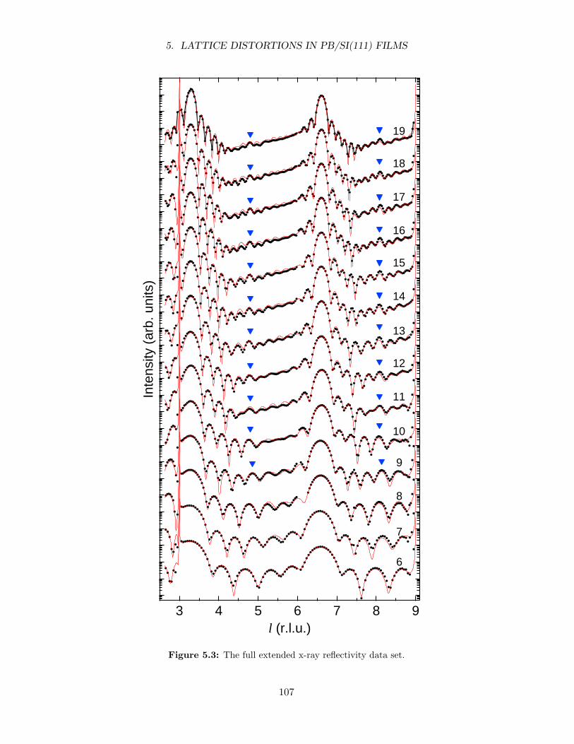
5. LATTICE DISTORTIONS IN PB/SI(111) FILMS
Inte
nsity
(ar
b. u
nits
)
9876543l (r.l.u.)
6
19
18
17
16
15
14
13
12
11
10
9
8
7
Figure 5.3: The full extended x-ray reflectivity data set.
107

5. LATTICE DISTORTIONS IN PB/SI(111) FILMS
Inte
nsity
(ar
b. u
nits
)
9876543l (r.l.u.)
18 AL
13 AL
7 AL
Experimental Data Model Fits No Layer Distortions
Figure 5.4: Extended x-ray reflectivity data (points) for selected cover-ages. The sharp peaks at l = 3 and 9 are the Si(111) and (333) Braggpeaks, respectively, while the interference fringes in-between are due to thePb overlayers. The areas marked by inverted triangles are half-order fea-tures indicative of a quasibilayer periodicity to the lattice structure of thePb film. Solid curves are fits using Method B described in the text. Dottedcurves are fits with uniform interlayer spacing in the film, which do notrepresent the data well, especially near the half-order features.
108

5. LATTICE DISTORTIONS IN PB/SI(111) FILMS
SU
BS
TR
AT
E VA
CU
UM
-8
-4
0
4
8
∆ 1
(%
0)
131197531Pb Layer
Figure 5.5: The internal lattice distortions for N = 14, calculated usingEq. (4.40) with the parameters from a fit to the extended x-ray reflectivity.Alternations in the distortions are evident, which leads to a quasibilayersuperperiod in the lattice structure, as shown with shaded boxes. Thiseffect manifests itself as a weak half-order superstructure peak in the x-rayprofiles, as seen in Figs. 5.3 and 5.4.
this wavelength is 1.98 A, which is close to 23 the bulk interlayer spacing
t0 = 2.84 A. Thus, every 2 AL of Pb roughly corresponds to an integralnumber of oscillations in the charge density. Since the relationship is notexact, the superperiodicity is quasibilayer, and the phase of even-odd oscil-lations can reverse over a sufficiently wide range of thicknesses.
Oscillations are evident in the lattice distortions resulting from the fitsto the x-ray reflectivity, an example of which is shown in Fig. 5.5 for N = 14.Most of the lattice relaxation occurs in the atomic layers closest to the twofilm boundaries, but the quasibilayer distortions penetrate deep into the filmas well. An instance of phase reversal (even-odd crossover) is also evident.The overall behavior reflects the force variations as shown in Fig. 4.6(b).The asymmetry of the values in Fig. 5.5 is due to different values for thetwo charge spillages ∆s and ∆0. The results for other thicknesses are qual-itatively similar. The thickness dependence of these lattice distortions orrelaxations is shown in Fig. 5.6, where the different sets of data points cor-respond to four different methods that were used to fit the x-ray data. Inall cases, the film structure factor was calculated using Eq. (2.40) with theintensity given by Eq. (2.44).
109

5. LATTICE DISTORTIONS IN PB/SI(111) FILMS
-5
0
5
∆
2,3
-5
0
5
∆
-2
-1
10
5
0∆
1,2
(%
0)
Model A Model B Averages
Model C Model D
-15
-10
-5
0
∆
-1
181614121086Pb Thickness
(AL)
(Nearest to Substrate)
(Nearest to Vacuum)
Figure 5.6: The lattice relaxations for the outer atomic layers for eachthickness N , where all values are in % t0. The different sets of data pointscorrespond to different fitting methods described in the text. The valuesfor Method A are the values calculated using the parameters for the dataset with coverage Θ = N AL. The points on the far right of each graphrepresent the values averaged over N for all four methods, along with errorbars deduced from the spread in the results.
110

5. LATTICE DISTORTIONS IN PB/SI(111) FILMS
Method A
The data for each coverage were fit separately with the lattice distor-tions described by Eq. (4.34), the local charge gradient model. To reducethe number of independent variables, parameters for the lattice distortionmodel were assumed to be independent of N for any particular coverage,but were allowed to be different for different coverages. This assumption isvalid for perfectly smooth films, but can be inaccurate for rough films. Sincethese parameters do depend on thickness and the film roughness is not nec-essarily negligible, the Debye-Waller parameter in Eq. (2.40) was replacedwith ζj factors, as in Eq. (2.39), but only for the Pb layers close to the filmboundaries. As a result, this method will be less reliable for extracting thethickness dependence of the lattice distortions, especially for higher cover-ages since they have the greatest degree of roughness. The results for thetwo outermost Pb atomic layers at each film interface are shown in Fig. 5.6as open circles, where the values for any particular thickness N are takenfrom the data set whose coverage is N AL (with a distribution of pN valuespeaked at that thickness).
Method B
The data for all 14 coverages were fit simultaneously using Eq. (4.34)for the lattice distortions. With this method, the parameters for the latticedistortion model were N -dependent and shared amongst all of the datasets. The other parameters needed to fit the data — the pN values, Debye-Waller factor, etc. — were separate for each coverage. The results forthe lattice relaxations of the outermost layers are shown in Fig. 5.6 as openupright triangles. Compared to Method A, this method involved fewer fittingparameters since no ζj factors were needed. Since the parameters of thelattice distortion model were N -dependent, this method is more likely toextract the thickness dependence of the interlayer relaxations.
Method C
As with Method B, all of the data sets for different coverages were fitsimultaneously, but with the lattice distortions calculated using the electro-static force model, Eq. (4.40). The same number of parameters were usedin the fits as with Method B. The results from this method are shown withopen inverted triangles in Fig. 5.6.
111

5. LATTICE DISTORTIONS IN PB/SI(111) FILMS
Method D
No model was used for the lattice distortions. Instead it was assumedthat any relaxations of the lattice would be limited to the atomic layersclosest to the interfaces. The two interlayer spacings closest to the substrateand the vacuum (four total) were fit as free parameters and were allowed tovary for different N . To keep the number of parameters reasonable, all 14data sets for different coverages were fit simultaneously as with Methods Band C, sharing the layer expansion parameters. The interlayer spacings forthe other Pb layers were assumed to be equal to a separate parameter, t,which introduces one additional parameter per data set to the fit comparedto Methods B and C. The results from this fit are shown as open squares inFig. 5.6.
5.4 Discussion and Comparison with Other
Studies
All four methods of analysis can be justified on physical grounds as reason-able models to describe the essential features of the system. They involvedifferent constraints on some aspects of the system and, in some cases, verydifferent numbers of fitting parameters, yet they all resulted in fits of compa-rable quality (measured by χ2). This is a strong indication that the modelsreflect the physical system. The spread in the results is an indication of thestandard error or level of confidence in the results. The black diamonds anderror bars at the right side of the panels in Fig. 5.6 show that, averagedover the thickness range of study, the top layer spacing of the Pb film iscontracted by 8.0 ± 2.4% relative to the bulk, while the next layer spacingis expanded by 2.2± 1.0%. These values are substantially larger than thosereported for bulk Pb(111) [87], but are closer to those resulting from recentfirst-principles calculations [88]. The layer spacing closest to the Si substrateis expanded by 5.8 ± 2.2%, and the next layer spacing is essentially bulk-like to within ±1.5%. In addition to these general trends that are related toFriedel oscillations associated with the film boundaries, the layer relaxationsexhibit quasibilayer oscillations as a function of film thickness that can beattributed to confinement and interference effects.
Results of the fits are shown as solid curves in Figs. 5.3 and 5.4. Thefits reproduce the aforementioned half-order features very well, especiallycompared to the example fits with no lattice distortions, shown as dottedcurves in Fig. 5.4. That being said, it was found that other solutions ex-
112

5. LATTICE DISTORTIONS IN PB/SI(111) FILMS
isted with χ2 values only slightly larger than the best fits. Such solutionsprimarily differed in the lattice relaxations for ∆t1,2 and ∆t2,3, the two in-terlayer spacings closest to the substrate. All solutions exhibited strongquasibilayer oscillations as a function of thickness; however, they differed inwhere the crossover from even to odd occurs — i.e., the phase of the oscilla-tions is weakly determined. For example, the turning point that is evidentat around N ≈ 17 in the data for ∆t1,2 in Fig. 5.6 was found at N ≈ 13 andN ≈ 11 in two other solutions with comparable χ2 values as the best fit. Allsolutions exhibited similar relaxation values for ∆tN−1,N and ∆tN−2,N−1,the relaxations of the layers closest to the vacuum. The greater uncer-tainty in the lattice distortions near the substrate may be due to interfacialroughness from the underlying Si(111) substrate, whose step heights will beincommensurate with the interlayer spacing of the Pb overlayers. However,these errors are no larger than the spread of values determined based on thefour different methods of analysis.
In this study, the penetration depth of the x rays used greatly exceededthe thicknesses of all the films studied, so the interference patterns in thedata are due to scattering from all the film overlayers. However, a techniquesuch as STM or HAS, with a short probing depth, will primarily measurethe step heights on the surface of the film (see for example Fig. 1.1). Tocompare with the results of such studies, Fig. 5.7 shows the deviation ofthe net film thicknesses from their ideal bulk values and the deduced stepheights as functions of N . Each thickness deviation value is the sum ofall the lattice distortions (i.e., the ∆tj,j+1 values) for any given N and thestep height values are defined as the difference between two net thicknessesdiffering by 1 AL. The error bars indicate the spread in values from thedifferent fitting methods. These values show clear quasibilayer oscillations,particularly for the smaller thicknesses. For larger thicknesses, the error barsget progressively wider, commensurate with the increase in film roughnessas shown in Figs. 5.1 and 5.2.
It should be noted that the term “step height” as used here refers to thevertical distances between the terrace heights of two thicknesses differing by1 AL. The local step height encountered by an atom diffusing across thesurface of the sample may be different, since additional lattice distortions inthe regions very near to the step edges probably occur to minimize the localstrain and shear energies. That is, the diagram in Fig. 2.10 is not indicativeof the local region around a step edge, but rather a schematic showing howthe atomic layers in the (terraces of) different regions of thickness may bemisaligned. Furthermore, lateral Friedel oscillations originating from the
113

5. LATTICE DISTORTIONS IN PB/SI(111) FILMS
6
4
2
0
-2Thi
ckne
ss D
evia
tion
(%
0)
-6
-3
0
3
6
Ste
p H
eigh
t Dev
iatio
n (%
0)
181614121086Nominal Pb Thickness
(AL)
(a)
(b)
Figure 5.7: (a) The net thicknesses calculated from the lattice distortions.Values are the deviation from the ideal thickness, Nt0, in % t0. Error barsare representative of the spread in values from the different fitting methodsdescribed in the text. (b) The deduced step heights at the surface, definedas the difference between every two adjacent points in (a).
step edges have been observed in the electron density [89, 90], which canalso affect the lattice structure. However, such edge effects will be limitedto a relatively local region (within a few lattice spacings) near the step edges.Since HAS is a scattering technique, it measures the statistical average ofthe scattering from the atomic planes, and STM studies generally measurethe heights of atomic terraces over an extended range. Thus, edge effectscan be neglected in such comparisons.
The oscillations in Fig. 5.7(b) are consistent with the STM results shownin Fig. 1.1, where it should be noted that the N values differ from thosepresented here by 1 AL since we have included the wetting layer in N .However, the amplitude of the oscillations in Fig. 5.7 is much smaller thanthat in Fig. 1.1(b), which may be partly attributable to the fact that STMmeasures the electron density at the surface, which may not reflect the true
114

5. LATTICE DISTORTIONS IN PB/SI(111) FILMS
positions of the atomic cores. Similarly, our results are also consistent withthose found in the HAS study of Ref. 18.
5.5 Summary
This chapter presented surface x-ray diffraction results of the growth andlayer structure (strain) of Pb/Si(111) films with thicknesses of 6–19 AL.At 110 K the system is found to follow a metastable layer-by-layer growthmode with increasing roughness. The extended x-ray reflectivity profileswere found to have distinctive half-order features present that are indicativeof a quasibilayer periodicity to the lattice structure. To describe the latticedistortions in the context of QSE, the free-electron models developed inChapter 4 are used that take into account the formation of quantum wellstates in the film and describe the Friedel-like oscillations in the electroniccharge density of the film. The free-electron models are found to explainthe quasibilayer lattice distortions of the film and enable a detailed fit of theexperimental data.
Extended x-ray reflectivity profiles at integer coverages were obtainedand analyzed to reveal the thickness dependence of the structural propertiesof the film. Quasibilayer oscillations are also observed in the outermostlattice relaxations as a function of thickness, similar to oscillations seen inother physical properties of the films due to QSE. Finally, the deviationsfrom the ideal film thicknesses are deduced and compared with previousSTM and HAS studies, where the present results are found to qualitativelyagree, albeit with a smaller amplitude of oscillation. It can be concludedthat quantum confinement has important effects on the physical structureof a nanoscale film.
115

6 Surface Energy ofPb/Si(111) Films
6.1 Experiment Overview
The relative stability of thin metal films has been shown to exhibit strongvariations as a function of thickness that have been attributed to elec-tronic contributions to the surface energy [26, 41, 44]. In addition, for cer-tain temperature ranges, some systems exhibit a peculiar film morphologywhere steep-sided, flat-topped islands of uniform height form on the sur-face (Fig. 1.2). Using x-ray diffraction and scanning tunneling spectroscopy,the formation of these “nanomesas” has been correlated with the electronicstructure of the films [15, 19, 20, 22–26]. This chapter presents a study ofthe morphological evolution of Pb films as a function of temperature. Thisevolution is explained in terms of QSE in the surface energy of the films, forwhich quantitative empirical information is obtained [84,91].
The experiment is a study of the structural evolution of smooth Pbfilms grown on Si(111) at 110 K as they are annealed to a state of localequilibrium near room temperature. By frequently interrupting the anneal-ing process and examining the film morphology, the system is effectivelyobserved exploring the local energy landscape as it evolves. Detailed discus-sions are presented for two different samples, one with an initial thicknessthat corresponds to a relatively stable configuration (low surface energy),and one with an initial thickness that is relatively unstable (high surface en-ergy). The structural evolution and thermal stability of the two films differmarkedly; however, analysis of their final quasi-equilibrium states producesthe same form for the surface energy, as expected. The annealing behavior ofthe films also reveals an additional effect; namely, after the initially smoothfilm breaks up, further annealing results in the formation of increasinglytaller islands. This effect is also attributed to quantum electronic effects.First principles calculations show that the most energetically favored con-figuration of the system consists of a single layer wetting the substrate (seeFig. 1.3); due to the initial volume of deposited film material, to conservemass the film morphology thus phase separates into surface regions coveredonly by a wetting layer, which has the lowest surface energy, and regions
116

6. SURFACE ENERGY OF PB/SI(111) FILMS
with islands of preferred heights. As the annealing temperature increases,the system has more thermal energy with which to rearrange the atoms onthe surface, resulting in the formation of taller islands and a correspondingincrease in the area covered by the wetting layer.
As in the experiment of Chapter 5, Pb films were grown in situ at 110 Kusing molecular beam epitaxy at a rate of 0.84 A/min. At this tempera-ture the system follows a metastable layer-by-layer growth mode that allowsfor monitoring of the coverage of the films during deposition by collectingthe reflected x-ray intensity at the lowest-order out-of-phase condition forPb(111), which exhibits layer-by-layer oscillations as described in Sec. 5.2.This technique allows for smooth films of precise coverage to be grown. Afterdeposition, the films were slowly annealed to progressively higher temper-atures in increments of approximately 5–10 K. After reaching each desiredannealing temperature, the sample was quenched back to 110 K for measure-ment of the specular extended x-ray reflectivity, which was obtained usingthe ridge scan method described in Sec. 3.6.
6.2 Extended X-Ray Reflectivity Analysis
Figures 6.1 and 6.2 show extended x-ray reflectivity data (points) for twosamples with initial coverages of 6 AL and 11 AL, respectively. The reflec-tivity profiles measured after annealing to the temperatures indicated areshown in progressive order starting from the base temperature at the bot-tom. Although data was collected every 5–10 K, only select temperaturesare shown to illustrate the major morphological changes. The sharp peaksat l = 3, 9, and 12 are the Si(111), (333), and (444) Bragg peaks, respec-tively, and the interference fringes in-between are due to the Pb overlayers.The broader peaks at l ≈ 3.3, 6.6, and 9.9 are the Pb(111), (222), and (333)Bragg peaks, respectively. The number and spacing of the fringes betweenthese peaks are an indication of the center of the thickness distribution of thefilm and its roughness. The reflectivity profiles for smooth films exhibit well-defined fringes with deep minima, similar to the N -slit interference functionshown in Fig. 2.9. In such a profile, the number of fringes is equal to thenumber of atomic layers in the film minus two. For example, the four well-defined fringes evident between the Pb Bragg peaks in the 110 K data inFig. 6.1 are indicative of a smooth film with a thickness of 6 AL. Thus, theappearance of additional fringes at intermediate temperatures indicates thatPb islands with larger thicknesses form on the surface. Detailed analysis ofthe data indicates that the average island height tends to get larger. That
117

6. SURFACE ENERGY OF PB/SI(111) FILMS
Inte
nsity
(ar
b. u
nits
)
1211109876543l (r.l.u.)
110 K
274 K
266 K
259 K
250 K
232 K
Figure 6.1: Extended x-ray reflectivity data (points) for a sample with acoverage of 6 AL after annealing to the temperatures indicated. Fits areshown as solid curves.
118

6. SURFACE ENERGY OF PB/SI(111) FILMS
Inte
nsity
(ar
b. u
nits
)
1211109876543
l (r.l.u.)
280 K
266 K
253 K
200 K
174 K
110 K
Figure 6.2: Extended x-ray reflectivity data (points) for a sample with acoverage of 11 AL after annealing to the temperatures indicated. Fits areshown as solid curves.
119

6. SURFACE ENERGY OF PB/SI(111) FILMS
is, the smooth film at 110 K breaks up into nanostructures that get higherwith increasing temperature. As discussed below, this curious behavior isrelated to a tendency for the system to favor the formation of surface regionscovered by only a single wetting layer and oscillations in the surface energysimilar to those calculated in Sec. 4.5 that favor the formation of islands ofspecific thicknesses.
The diminished fringes at the highest annealing temperatures indicatea relatively rough film. A broad distribution of thicknesses present on thesurface should result in a relatively featureless reflectivity profile in-betweenthe Pb Bragg peaks. However, in both sets of data small oscillations areevident roughly halfway between these peaks. Since these features occurclose to the half-order position for Pb, they are indicative of a bilayer orquasibilayer periodicity in the film structure. In Chapter 5, enhanced half-order features due to quasibilayer distortions in the film layer structurewere observed in smooth Pb films. However, as is shown below, due to filmroughness such lattice distortions do not explain the half-order oscillationsin this case. Rather, they can be attributed to a bilayer or quasibilayerperiodicity in the thickness distribution pN .
To illustrate the information content of these near-half-order oscillationsand to show this effect is not due to lattice distortions, simulated reflectivityprofiles were calculated for various thickness distributions with the atomiclayer positions calculated using the local density gradient model of Sec. 4.4.2,which was found to accurately describe the lattice structure of Pb films inChapter 5. Figure 6.3(a) shows the reflectivity for a rough sample with aGaussian distribution of thicknesses as shown in Fig. 6.4(a). Even with thepresence of quasibilayer lattice distortions, the broad distribution of thick-nesses in the film obscures any half-order feature in the curve of Fig. 6.3(a).However, half-order oscillations are present in the simulated reflectivity ofa sample that has a preference for either even or odd thicknesses, as shownin Fig. 6.3(b) with the distribution used shown in Fig. 6.4(b). However, thepositioning of the oscillations in this case, exactly centered at the half-orderposition of l ≈ 5, does not coincide with the positioning of the oscillations inthe experimental data shown at the bottom of Fig. 6.3 (which is the 280 Kdata from Fig. 6.2), as is highlighted with the vertical dotted line. Theshifting of the near-half-order oscillations observed can be reproduced bymodifying the bilayer distribution of thicknesses so that the preference foreven or odd thicknesses switches periodically, as shown in Fig. 6.4(c). Suchan effect is expected due to the beating patterns found in the surface energyin Sec. 4.5. The corresponding reflectivity for such a simulation is shown in
120
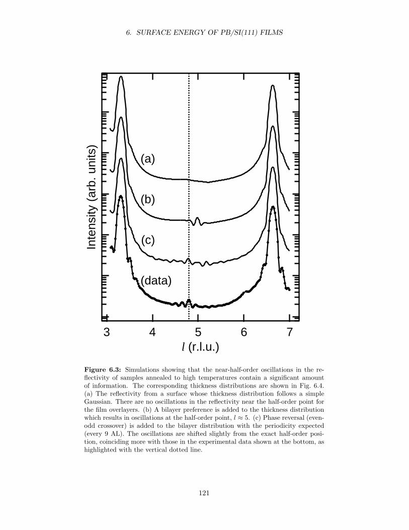
6. SURFACE ENERGY OF PB/SI(111) FILMS
Inte
nsity
(ar
b. u
nits
)
76543l (r.l.u.)
(a)
(b)
(c)
(data)
Figure 6.3: Simulations showing that the near-half-order oscillations in the re-flectivity of samples annealed to high temperatures contain a significant amountof information. The corresponding thickness distributions are shown in Fig. 6.4.(a) The reflectivity from a surface whose thickness distribution follows a simpleGaussian. There are no oscillations in the reflectivity near the half-order point forthe film overlayers. (b) A bilayer preference is added to the thickness distributionwhich results in oscillations at the half-order point, l ≈ 5. (c) Phase reversal (even-odd crossover) is added to the bilayer distribution with the periodicity expected(every 9 AL). The oscillations are shifted slightly from the exact half-order posi-tion, coinciding more with those in the experimental data shown at the bottom, ashighlighted with the vertical dotted line.
121

6. SURFACE ENERGY OF PB/SI(111) FILMS
5
0
(% S
urfa
ce A
rea
Cov
ered
)
403020100Pb Thickness
(AL)
5
0
5
0
5
0
(a)
(b)
(c)
(d)
Figure 6.4: The thickness distributions used in the simulations of Fig. 6.3. (a)A simple Gaussian distribution. (b) A dual-Gaussian distribution where the upperenvelope dictates the values for odd N . (c) The same dual-Gaussian distributionwith an even-odd crossover every 9 AL, the expected period of the beating functionin the surface energy. (d) The distribution resulting from a fit to the experimentaldata in Fig. 6.3(d), starting from the distribution in (c). In all cases, the coverageof the film, Eq. (2.43), is constrained to 11 AL (the coverage of the film whose datais shown) and the wetting layer, p1, was adjusted such that the surface formed aclosed film [Eq. (2.42)].
122

6. SURFACE ENERGY OF PB/SI(111) FILMS
Fig. 6.3(c), where it can be seen that the near-half-order oscillations are nowin phase with those in the data, although they are not reproduced exactly.By letting the pN be independent parameters and using the values shownin Fig. 6.4(c) as an initial condition, an accurate fit to the data can be ob-tained, the results of which are shown in Fig. 6.4(d). Thus, the presenceof the near-half-order oscillations in the data and their position relative tothe Pb Bragg peaks is indicative of quasibilayer oscillations in the thicknessdistribution.
Detailed information on the surface morphology was obtained by fittingeach reflectivity profile using Eq. (2.47) to obtain the thickness distributionpresent on the surface, pN. Each pN parameter was ultimately fit asan independent parameter except for p1, the coverage of the wetting layer,which was constrained such that Eq. (2.42) was satisfied. At the higherannealing temperatures, when the distribution of thicknesses present on thesurface is broad, the number of non-zero pN values needed to describe thesurface morphology is large. Local minima in parameter space were avoidedby starting the fit for each temperature (except the first) from the best fitof the previous temperature, effectively following the film morphology as itevolves. Due to the large number of independent parameters used in someof the fits, the sensitivity of the fits to any individual pN value was weak;however, as demonstrated with Figs. 6.3 and 6.4, the overall distributionof pN values is well-determined by the information contained in the near-half-order oscillations in the x-ray reflectivity profiles. As a consequence,given the confidence in the form of the thickness distribution demonstratedabove, the relative errors are estimated to be within 10% of each pN value.The partial coherence factor in Eq. (2.47) was found to be near unity (allcoherent scattering) for the lower annealing temperatures and on the orderof 0.5 for the highest temperatures, consistent with a surface morphologythat consists of many different height nanomesas that each extend laterallyfor significant distances.
6.3 Evolution of Film Morphology with
Annealing
The thickness distributions determined from the fits to the reflectivity datain Fig. 6.1 are shown in Fig. 6.5. After deposition at 110 K, the thicknessdistribution is sharply peaked about N = 6, corresponding to a very smoothfilm with a rms roughness of about 1.3 A. Upon annealing, no discernablechanges in the reflectivity profile are observed until 232 K, at which point
123

6. SURFACE ENERGY OF PB/SI(111) FILMS
regions of 8 and 10 AL start to form. These regions then become moreprevalent by 250 K and the residual 7 AL region has disappeared, which is aless-stable thickness. The dominant thickness of the film is still 6 AL up to266 K, though, at which point the distribution has broadened significantly.At 274 K, the preference for 6 AL due to the initial condition has disappearedand the surface has presumably reached a state of local equilibrium in whicheach thickness N is in equilibrium with its neighboring thicknesses N ±1. The rms roughness at this temperature is about 18 A. The thicknessdistributions show a clear preference for certain thicknesses over others witha quasibilayer periodicity, which is expected because of the near-half-orderoscillations present in the extended x-ray reflectivity profiles, as discussed inthe last section. Two of the expected even-odd crossover points are evidentas well at N ≈ 5 and N ≈ 14.
Phenomenologically, the fact that the thickness distribution gets broaderafter annealing is actually expected when one considers that the system fol-lows a Stranski-Krastanov growth mode at room temperature, where islandsform on top of a single wetting layer. However, in this case the distributionof thicknesses not only broadens, but its center moves upwards in N . Thatis, at lower temperatures, the distributions in Fig. 6.5 are peaked about theinitial thickness of 6 AL, but at the final temperature, the average structureheight above the wetting layer is about 12 AL, which implies that on aver-age the surface features are getting higher with increasing temperature. Toconserve the amount of Pb on the surface, the initially smooth film mustbreak up into islands separated by increasingly wide regions of the surfacecovered only by a wetting layer. The amount of the surface covered by onlya wetting layer, p1, found in our analysis is shown in Fig. 6.6. It increasesmonotonically with the annealing temperature. The most stable configura-tion of the system is to maximize the coverage of the wetting layer, which issupported by first-principles calculations that show a deep global minimumat N = 1 in the surface energy (see Fig. 1.3). However, the system cannotfully maximize the coverage of the bare wetting layer due to kinetic limi-tations and thermal fluctuations that will tend to roughen the surface andfavor a reasonable nanostructure height. The combination of these effectsexplains the annealing behavior observed.
In contrast to the 6 AL film, whose initial thickness persisted throughmost of the annealing process, indicating that this thickness is preferred,films with initial thicknesses that are not preferred exhibit a qualitativelydistinct behavior. Figure 6.7 shows the thickness distributions for the filmwith an initial coverage of 11 AL (Fig. 6.2) and its morphological changes
124

6. SURFACE ENERGY OF PB/SI(111) FILMS
50
0
(% S
urfa
ce A
rea
Cov
ered
)
2218141062Pb Thickness
(AL)
50
0
20
0
10
0
10
0
5
0
110 K
232 K
250 K
259 K
266 K
274 K
Figure 6.5: The coverage of different thicknesses present on the sample surfacefor each corresponding curve in Fig. 6.1, with the annealing temperatures indi-cated. The coverage values were determined via a fit using a model described inthe text. The surface evolution is shown to evolve from a very smooth film at 110 Kthrough various metastable “preferred thickness” states before reaching a state oflocal equilibrium. The preference of certain thicknesses over others corresponds toquasibilayer oscillations in the surface energy. The dotted line through the 274 Kdata is the result of applying a binomial filtering algorithm to the values for ananalysis of the surface energy.
125

6. SURFACE ENERGY OF PB/SI(111) FILMS
50
40
30
20
10
0 1
(% S
urfa
ce A
rea)
270250230110Annealing Temperature (K)
Figure 6.6: The amount of the 6 AL sample surface covered only by asingle wetting layer increases with temperature. The surface energy has adeep global minimum at N = 1 that results in the wetting layer being themost stable configuration of the system.
upon annealing to the indicated temperatures. As with the 6 AL film, theinitial distribution is sharply peaked about the initial thickness, consistentwith a layer-by-layer growth mode. However, in this case the initially smoothfilm (3.2 A rms roughness) begins to break up at a much lower temperatureof 174 K. By 200 K, the coverage of the initial 11 AL has largely disappearedand the film has bifurcated into the neighboring thicknesses of 10 and 12 AL,both of which are more stable than 11 AL. At 253 K, the surface is dominatedby regions of 12 AL, resulting from phase separation of the system into astate corresponding to a local minimum in the surface energy at N = 12and a state in the global minimum at N = 1. It is this temperature rangein which uniform height nanomesas have been observed in many microscopystudies [15, 19, 20, 22–25]. Annealing to higher temperatures results in abroadening of the thickness distribution until at 280 K, when the residualpreference for 12 AL from the uniform height phase has disappeared, the filmhas reached local equilibrium (28 A rms roughness). Since we started witha thicker film, there are more Pb atoms to rearrange and nanostructuresof larger height are able to form on the surface. The final distributionof thicknesses is correspondingly much broader and has a higher averagestructure height above the wetting layer of approximately 18 AL. As a result,the oscillations in the distribution, which are indicative of variations in therelative stability of different thicknesses, are present over a wider range,allowing a more comprehensive analysis of the surface energy.
126

6. SURFACE ENERGY OF PB/SI(111) FILMS
20
0
(
% S
urfa
ce A
rea
Cov
ered
)
3430262218141062
Pb Thickness
(AL)
20
0
40
20
0
40
20
0
10
0
5
0
110 K
174 K
200 K
253 K
266 K
280 K
Figure 6.7: Evolution of the structure of the 11 AL film after annealing to the tem-peratures indicated, obtained from fits to the extended reflectivity data in Fig. 6.2.In contrast to the 6 AL film, which is a stable thickness, this film bifurcates atthe comparatively low temperature of 174 K. Due to the higher volume (coverage)of Pb in the film, the final distribution of thicknesses is broader and peaked at agreater thickness than that in Fig. 6.5, providing information about the surfaceenergy over a broader range of thicknesses.
127

6. SURFACE ENERGY OF PB/SI(111) FILMS
6.4 Surface Energy
The variations in the thickness distributions of Figs. 6.5 and 6.7 are indica-tive of a relative preference for certain thicknesses over others. An exper-imental measure of the relative stability of a thickness can be obtained bycomparing the fractional surface area it covers with that of its neighbors
pN − pN−1 + pN+1
2= −1
2p′′N (6.1)
where p′′N is the discrete second derivative of pN . That is, thicknesses forwhich the local curvature of pN is negative (p′′N < 0) are relatively stable,since they cover more of the sample surface compared with their neighboringthicknesses. Conversely, if the local curvature of pN is positive (p′′N > 0), thethickness N is relatively unstable since the system prefers to form regionswith thicknesses of N±1 over N . The values of p′′N for the highest annealingtemperature data in Figs. 6.5 and 6.7 are shown as solid circles in Figs. 6.8(a)and 6.8(b), respectively. In both cases, quasibilayer oscillations about p′′N =0 are evident, a reflection of variations in the relative stability of differentthicknesses. As mentioned above, the 11 AL sample provides informationover a wider range of thicknesses than the 6 AL sample due to its greaterinitial thickness.
This effect will manifest itself as corresponding variations in the surfaceenergy, similar to those seen in the free-electron calculations of Sec. 4.5. Wecan extract empirical information about the surface energy by relating it tothe pN parameters, which should follow a Boltzmann distribution
pN = X e−ES(N)/kBT (6.2)
where kB is Boltzmann’s constant and T is taken to be the annealing temper-ature. In the case of a system that is in global thermodynamic equilibrium,X is simply a constant of proportionality. However, in the present case itis only assumed that the system is in a state of local equilibrium, in whichcase X is a slowly varying function of N . Thus, X will depend on a varietyof factors, including the film’s annealing history. To remove this ill-definedfunction from the analysis, the self-normalized local variations in pN areconsidered instead:
δpN ≡ pN − pN
pN
(6.3)
where pN is a local average of pN . Such a quantity corresponds to thesmoothly varying background underlying the oscillations in the pN values
128

6. SURFACE ENERGY OF PB/SI(111) FILMS
-10
0
10
Data Fit
-40
-20
0
20
40
(m
eV)
30252015105Pb Thickness (AL)
-5
0
5
(a)
(b)
(c)
11 AL
6 AL
Figure 6.8: The discrete second derivative of the pN values for the 274 K and 280 Kdata in Figs. 6.5 and 6.7 are shown as solid circles in (a) and (b), respectively. Two-parameter fits to these data as described in the text are shown as open circles, whichaccurately reproduce the quasibilayer oscillations and envelope beating functions.(c) The surface energy as calculated using Eq. (4.52) with the average parametersfrom the two fits in (a) and (b). Dashed lines show the beating envelopes for theexperimental values in (a) and (b) and the calculated values in (c). Vertical dottedlines indicate the nodes in the beating envelope of the surface energy in (c), whichcorrespond closely to the nodes in (a) and (b).
129

6. SURFACE ENERGY OF PB/SI(111) FILMS
of Figs. 6.5 and 6.7. As long as pN is calculated using only a small local setof pN values, X can be regarded as being approximately constant over thisset and δpN is independent of X . A reasonable method for calculating thelocal average is to use a binomial filtering algorithm [92]
pN =pN−1 + 2pN + pN+1
4. (6.4)
The pN values resulting from the application of this algorithm to the top pN
distributions in Figs. 6.5 and 6.7 are shown as dotted curves, which showthat it indeed produces smooth curves. Using this algorithm also has theadditional benefit that δpN is simply related to the discrete second derivativeof pN
δpN =−p′′N4pN
. (6.5)
The empirical discrete second derivative values in Figs. 6.8(a) and 6.8(b)were fit using the function
(p′′N
)theory
= −4 (pN )expt (δpN )theory , (6.6)
where the theoretical version of δpN is
(δpN )theory =4pN
pN−1 + 2pN + pN+1− 1, (6.7)
with the pN values calculated using Eq. (6.2) and the sinusoidal approxima-tion for the surface energy found from the free-electron model calculation,Eq. (4.52). Note that when this form for ES is used, the constant offset inEq. (4.52), B, cancels from Eq. (6.7). Due to a significant covariance foundbetween the parameters A and α, where the adjustment of one parametercould be largely compensated for by a complementary adjustment of theother, the value for the decay exponent found in Sec. 4.5, α = 1.77, wasfixed in the fits. The analysis was found to be relatively insensitive to thespecific value of the decay exponent, as long as it was between 0.9 < α < 2.0.Similar fits with α = 1 yield comparable surface energies that differ by lessthan 3 meV for most of the thickness range available. The Fermi wave vec-tor was taken to be the empirical value for bulk Pb(111), kF = 1.59 A−1.Thus, only two adjustable parameters were used in the fits: A and φ. Thefitted value of φ was (0.49 ± 0.01)π for both fits and the fitted value of A
was 1.0±0.3 eV for the 6 AL sample and 1.3±0.2 eV for the 11 AL sample.The surface energy shown in Fig. 6.8(c) was calculated using the average ofthese two values.
130
6. SURFACE ENERGY OF PB/SI(111) FILMS
6.5 Discussion
The annealing behavior of the two films is consistent with the surface energyshown in Fig. 6.8(c). At low temperatures, the system is kinetically limitedand can therefore be found in a metastable state where the predominantthickness is energetically unfavorable, as with the 11 AL film in this study.However, as the film is annealed and given more thermal energy, the unstable11 AL thickness easily bifurcates into the energetically preferred thicknessesof 10 and 12 AL. Upon further annealing, in some cases the film coalescesinto a state where the surface is mostly covered by islands of uniform height.For the initial 11 AL film, the preferred thickness of the islands (nanomesas)is 12 AL, which is actually indicated to have a higher surface energy than10 AL in Fig. 6.8(c). However, the system is prevented from forming uniform10 AL islands since this thickness is smaller than the initial thickness, andthe deep minimum in the surface energy for N = 1 favors the formation ofsurface regions covered only by a single wetting layer. As a consequence,a state that consists of 12 AL islands separated by regions of the surfacecovered only by the wetting layer is favored over a state in which both 10and 12 AL islands are present.
In contrast, for a film whose initial predominant thickness is more stable,like the 6 AL film in this study, the surface morphology remains unchangedup to a much higher temperature. When it does begin to evolve, the initial6 AL portion of the film is mostly retained while the unstable thicknesses(e.g., 7 AL) transform into higher stable thicknesses. The coverage of theinitial thickness in this case only slowly decays with increasing temperatureuntil local equilibrium is attained. We have collected similar data for otherinitial thicknesses, both preferred and not preferred, the annealing behaviorof which is consistent with the results presented here.
The overall phase shift of the surface energy and its envelope beatingfunction depend only on the boundary conditions at the film interfaces. Assuch, the nodal points in the surface energy envelope (the points where even-odd crossover occurs) should be found in the same places for the two datasets, which is indeed the case as seen in Fig. 6.8. Due to the symmetricboundary conditions used in the free-electron model of Sec. 4.5, the phaseshift in the surface energy calculated from it is different from the experi-mentally determined phase shift, as one would expect. The amplitudes ofoscillation found experimentally appear to be significantly greater than thefree-electron amplitude; however, they are consistent with the amplitudefound in the first-principles calculations shown in Fig. 1.3. The nodes in the
131

6. SURFACE ENERGY OF PB/SI(111) FILMS
beating envelope occur with the periodicity expected given the bulk Fermienergy, although there is a slight discrepancy for the first node at N ≈ 5 (seedotted vertical lines in Fig. 6.8). In this thickness region, interface effects aremore significant and the free-electron approximation of the surface energy,Eq. (4.52), becomes less accurate. However, the empirical stability datafor the lower N values in Figs. 6.8(a) and (b) is supported by independentphotoemission measurements [41], indicating that the data are reliable.
6.6 Summary
This chapter presented temperature-dependent x-ray diffraction data show-ing the morphological evolution of Pb films grown on Si(111) substrates.The films were grown at 110 K, at which temperature the system follows ametastable layer-by-layer growth mode. By annealing the films to around280 K in increments of 5–10 K, the surface morphology was observed passingthrough various metastable states before reaching a roughened state char-acterized by local equilibrium. The annealing behavior of two films withdifferent initial thicknesses clearly shows that certain film thicknesses aremore stable than others. A film with an initial thickness that is relativelystable (6 AL) remained intact up until approximately 230 K, at which pointit began to roughen and explore the broader energy landscape. In contrast,a film with an initial thickness that is relatively unstable (11 AL) beganto break up at the comparatively low temperature of 170–200 K, at whichpoint it decomposed (phase separated) into regions of thicknesses with lowersurface energies (islands dominated by a single height, 12 AL, surroundedby regions covered by the wetting layer only). This phenomenon of preferredheights can be explained by the phase separation of the system into a statecorresponding to a local minimum in the surface energy (the uniform-heightislands) and a state in the global minimum (the wetting layer).
In Sec. 4.5, the oscillations in the free-electron surface energy were foundto closely follow a damped sinusoidal form with a wavelength of λF /2. Thisresult is used to relate the details of the broad thickness distributions of theannealed films to their surface energy. These results draw a direct empiricallink between the formation of quantized electronic states due to confinementof the itinerant electrons to a metal film (QSE) and the relative stability ofdifferent film thicknesses, which can exhibit large variations for sizes differingby as little as a single atomic layer. Understanding such effects is criticalfor the engineering of metallic nanoscale devices.
132

7 Conclusions and Outlook
This dissertation has presented research on size-dependent quantum elec-tronic effects in ultrathin Pb/Si(111) films. These quantum size effects areinvestigated both theoretically with models based on a confined free-electrongas as well as experimentally with surface x-ray diffraction. The theoreticalmodels predict quasibilayer variations both in the atomic-layer structure ofthe films as well as their surface energy as a function of thickness. Thesepredictions are subsequently confirmed experimentally. In a layer-resolvedstudy of smooth films of thicknesses 6–19 AL, distinctive features appearin the extended x-ray reflectivity spectra indicative of lattice distortions inthe films with a quasibilayer superperiodicity. Detailed analysis reveals thatthese lattice distortions vary for different thickness films, again with a quasi-bilayer periodicity. In another experiment, the energetics of the system isinvestigated by annealing initially smooth Pb films to progressively highertemperatures, which causes the metastable films to break up into differentheight nanostructures. The structural evolution of these film nanostructuresis observed throughout the annealing process, which reveals quasibilayervariations in the relative stability of the film structures as a function ofheight (film thickness). These variations are directly linked to oscillationsin the surface energy similar to those calculated with the theoretical mod-els. Together, these studies have determined that the effects of quantumconfinement on atomic-scale metal structures can be dramatic and have asignificant impact both on the lattice structure and the thermal stability ofsuch nanostructures and films.
As always, there are many more directions in which this research couldcontinue. For example, it would be interesting to see if the effects describedin this work are also present in ultrathin liquid metal films. If a metal filmwith a thickness in the quantum regime could be prepared in the liquidstate on a semiconductor substrate, then the properties of the film couldconceivably be examined as a continuous function of thickness, which is incontrast with the integer number of atomic layers to which one is limitedwith epitaxial films. Another avenue of research that is currently being pur-sued is a real-time reflectivity study of the growth and annealing behaviors
133

7. CONCLUSIONS AND OUTLOOK
of Pb/Si(111) films. In such a study, the reflectivity rod is measured byscanning the incident angle of the x rays while a range of exiting beamsis collected simultaneously with an area detector such as a charge-coupleddevice (CCD). With this method, the rod can be measured in ∼2 min, an-other order-of-magnitude improvement over the ridge scan method outlinedin Sec. 3.6.2. Using this technique, real-time studies can be readily per-formed of the growth of these films at different growth temperatures and/orgrowth rates. By exploring the temperature/growth-rate parameter space,one can deduce information on the kinetic barriers that are involved in thepeculiar morphology that these films exhibit. In addition, the quantum sizeeffects described here are found in a variety of other properties of metalnanostructures, the details of which remain unexplored in many cases. Anexcellent example of one such property is the superconducting transitiontemperature. Preliminary results from other research groups [7, 8] appearto show variations in Tc for thin Pb films with a bilayer periodicity, similarto the those observed in the surface energy reported here. However, thesedata are not comprehensive and many details of the effect remain unknownor unexplored.
In conclusion, it is clear that quantum electronic effects play a significantrole in the physical characteristics of nanoscale metallic structures. Theseproperties can deviate significant from their bulk counterparts. As the sizeof technological devices settles more firmly in the quantum regime, thesesize-dependent effects will be of utmost importance.
134

References
[1] F. K. Schulte. “A theory of thin metal films: electron density, potentialsand work function.” Surf. Sci. 55, 427 (1976).
[2] S. Ciraci and I. P. Batra. “Theory of the quantum size effect in simplemetals.” Phys. Rev. B 33, 4294 (1986).
[3] P. J. Feibelman. “Static quantum-size effects in thin crystalline, simple-metal films.” Phys. Rev. B 27, 1991 (1983).
[4] G. A. Sorokin. “Influence of the surface scattering on the quantum sizeeffect.” Sov. Phys. Solid State 15, 1231 (1973).
[5] J. M. Blatt and C. J. Thompson. “Shape resonances in superconductingthin films.” Phys. Rev. Lett. 10, 332 (1963).
[6] B. G. Orr, H. M. Jaeger, and A. M. Goldman. “Transition-temperatureoscillations in thin superconducting films.” Phys. Rev. Lett. 53, 2046(1984).
[7] Y. Guo, Y.-F. Zhang, X.-Y. Bao, T.-Z. Han, Z. Tang, L.-X. Zhang,W.-G. Zhu, E. G. Wang, Q. Niu, Z. Q. Qiu, J.-F. Jia, Z.-X. Zhao, andQ.-K. Xue. “Superconductivity modulated by quantum size effects.”Science 306, 1915 (2004).
[8] T.-C. Chiang. “Superconductivity in thin films.” Science 306, 1900(2004).
[9] N. Trivedi and N. W. Ashcroft. “Quantum size effects in transportproperties of metallic films.” Phys. Rev. B 38, 12298 (1988).
[10] I. Vilfan, M. Henzler, O. Pfennigstorf, and H. Pfnur. “Anomalous thick-ness dependence of the Hall effect in ultrathin Pb layers on Si(111).”Phys. Rev. B 66, 241306(R) (2002).
[11] P. Saalfrank. “Quantum size effects in thin lead films.” Surf. Sci. 274,449 (1992).
[12] I. B. Altfeder, K. A. Matveev, and D. M. Chen. “Electron fringes on aquantum wedge.” Phys. Rev. Lett. 78, 2815 (1997).
[13] J. J. Paggel, C. M. Wei, M. Y. Chou, D.-A. Luh, T. Miller, and T.-C. Chiang. “Atomic-layer-resolved quantum oscillations in the workfunction: Theory and experiment for Ag/Fe(100).” Phys. Rev. B 66,233403 (2002).
135

REFERENCES
[14] P. J. Feibelman and D. R. Hamann. “Quantum-size effects in workfunctions of free-standing and adsorbed thin metal films.” Phys. Rev.B 29, 6463 (1984).
[15] M. Hupalo and M. C. Tringides. “Correlation between height selec-tion and electronic structure of the uniform height Pb/Si(111) islands.”Phys. Rev. B 65, 115406 (2002).
[16] A. Mans, J. H. Dil, A. R. H. F. Ettema, and H. H. Weitering. “Quantumelectronic stability and spectroscopy of ultrathin Pb films on Si(111)7×7.” Phys. Rev. B 66, 195410 (2002).
[17] A. Crottini, D. Cvetko, L. Floreano, R. Gotter, A. Morgante, andF. Tommasini. “Step height oscillations during layer-by-layer growthof Pb on Ge(001).” Phys. Rev. Lett. 79, 1527 (1997).
[18] J. Braun and J. P. Toennies. “Observation of a quantum size effect inthe surface electron density of thin lead films.” Surf. Sci. 384, L858(1997).
[19] W. B. Su, S. H. Chang, W. B. Jian, C. S. Chang, L. J. Chen, and T. T.Tsong. “Correlation between quantized electronic states and oscillatorythickness relaxations of 2D Pb islands on Si(111)-(7x7) surfaces.” Phys.Rev. Lett. 86, 5116 (2001).
[20] W.-B. Su, S.-H. Chang, C.-S. Chang, L. J. Chen, and T. T. Tsong.“Quantum size effects in low-temperature growth of Pb islands onSi(111)7x7 surfaces.” Jap. J. Appl. Phys. 40, 4299 (2001).
[21] R. Otero, A. L. Vazquez de Parga, and R. Miranda. “Observation ofpreferred heights in Pb nanoislands: A quantum size effect.” Phys. Rev.B 66, 115401 (2002).
[22] K. Budde, E. Abram, V. Yeh, and M. C. Tringides. “Uniform, self-organized, seven-step height Pb/Si(111)-(7× 7) islands at low temper-atures.” Phys. Rev. B 61, R10602 (2000).
[23] M. Hupalo, S. Kremmer, V. Yeh, L. Berbil-Bautista, E. Abram, andM. C. Tringides. “Uniform island height selection in the low tempera-ture growth of Pb/Si(111)-(7x7).” Surf. Sci. 493, 526 (2001).
[24] V. Yeh, L. Berbil-Bautista, C. Z. Wang, K. M. Ho, and M. C. Tringides.“Role of the metal/semiconductor interface in quantum size effects:Pb/Si(111).” Phys. Rev. Lett. 85, 5158 (2000).
[25] M. Hupalo, V. Yeh, L. Berbil-Bautista, S. Kremmer, E. Abram, andM. C. Tringides. “Uniform height island growth of Pb on Si(111)-Pb(
√3×√3) at low temperatures.” Phys. Rev. B 64, 155307 (2001).
[26] H. Hong, C.-M. Wei, M. Y. Chou, Z. Wu, L. Basile, H. Chen, M. Holt,and T.-C. Chiang. “Alternating layer and island growth of Pb on Si by
136

REFERENCES
spontaneous quantum phase separation.” Phys. Rev. Lett. 90, 076104(2003).
[27] L. Gavioli, K. R. Kimberlin, M. C. Tringides, J. F. Wendelken, andZ. Zhang. “Novel growth of Ag islands on Si(111): Plateaus with asingular height.” Phys. Rev. Lett. 82, 129 (1999).
[28] L. Huang, S. J. Chey, and J. H. Weaver. “Metastable structures andcritical thicknesses: Ag on Si(111)-7×7.” Surf. Sci. 416, L1101 (1998).
[29] C. M. Wei and M. Y. Chou. “Theory of quantum size effects in thinPb(111) films.” Phys. Rev. B 66, 233408 (2002).
[30] W. B. Jian, W. B. Su, C. S. Chang, and T. T. Tsong. “Vertical friedeloscillations in interface-induced surface charge modulations of ultrathinquantum islands.” Phys. Rev. Lett. 90, 196603 (2003).
[31] B. J. Hinch, C. Koziol, J. P. Toennies, and G. Zhang. “Single anddouble layer growth mechanisms induced by quantum size effects in Pbfilms deposited on Cu(111).” Vacuum 42, 309 (1991).
[32] M. Valden, X. Lai, and D. W. Goodman. “Onset of catalytic activity ofgold clusters on titania with the appearance of nonmetallic properties.”Science 281, 1647 (1998).
[33] N. D. Lang and W. Kohn. “Theory of metal surfaces: Charge densityand surface energy.” Phys. Rev. B 1, 4555 (1970).
[34] Z. Zhang, Q. Niu, and C.-K. Shih. ““Electronic growth” of metallicoverlayers on semiconductor substrates.” Phys. Rev. Lett. 80, 5381(1998).
[35] T. Valla, M. Kralj, A. Siber, M. Milun, P. Pervan, P. D. Johnson, andD. P. Woodruff. “Oscillatory electron-phonon coupling in ultra-thinsilver films on V(100).” J. Phys.: Condens. Matter 12, L477 (2000).
[36] T.-C. Chiang. “Photoemission studies of quantum well states in thinfilms.” Surf. Sci. Rep. 39, 181 (2000).
[37] L. Aballe, A. Barinov, A. Locatelli, S. Heun, and M. Kiskinova. “Tuningsurface reactivity via electron quantum confinement.” Phys. Rev. Lett.93, 196103 (2004).
[38] D.-A. Luh, T. Miller, J. J. Paggel, and T.-C. Chiang. “Large electron-phonon coupling at an interface.” Phys. Rev. Lett. 88, 256802 (2002).
[39] G. Materzanini, P. Saalfrank, and P. J. D. Lindan. “Quantum sizeeffects in metal films: energies and charge densities of Pb(111) grownon Cu(111).” Phys. Rev. B 63, 235405 (2001).
137

REFERENCES
[40] D. Schmicker, T. Hibma, K. A. Edwards, P. B. Howes, J. E. Macdon-ald, M. A. James, M. Breeman, and G. T. Barkema. “Low-temperaturegrowth of thin Pb layers and the quantum size effect.” J. Phys.: Con-dens. Matter 9, 969 (1997).
[41] M. H. Upton, C. M. Wei, M. Y. Chou, T. Miller, and T.-C. Chiang.“Thermal stability and electronic structure of atomically uniform Pbfilms on Si(111).” Phys. Rev. Lett. 93, 026802 (2004).
[42] J.-H. Cho, K. S. Kim, C. T. Chan, and Z. Zhang. “Oscillatory energeticsof flat Ag films on MgO(001).” Phys. Rev. B 63, 113408 (2001).
[43] C. M. Wei and M. Y. Chou. “Effects of the substrate on quantumwell states: A first-principles study for Ag/Fe(100).” Phys. Rev. B 68,125406 (2003).
[44] D.-A. Luh, T. Miller, J. J. Paggel, M. Y. Chou, and T.-C. Chiang.“Quantum electronic stability of atomically uniform films.” Science292, 1131 (2001).
[45] A. R. Smith, K.-J. Chao, Q. Niu, and C.-K. Shih. “Formation of atom-ically flat silver films on GaAs with a “silver mean” quasi periodicity.”Science 273, 226 (1996).
[46] E. Ganz, I. Hwang, F. Xiong, S. K. Theiss, and J. Golovchenko. Surf.Sci. 257, 259 (1991).
[47] M. J. Hadley, S. P. Tear, and T. N. Doust. J. Phys. Cond. Matt. 3,S277 (1989).
[48] P. B. Howes, K. A. Edwards, D. J. Hughes, J. E. Macdonald, T. Hibma,T. Bootsma, and M. A. James. “Influence of interfacial atomic structureon the Schottky-barrier height of Si(111)-Pb.” Phys. Rev. B 51, 17740(1995).
[49] P. B. Howes, K. A. Edwards, J. E. Macdonald, T. Hibma, T. Bootsma,M. A. James, and C. L. Nicklin. “The atomic structure of the Si(111)-(√
3×√3)-Pb reconstruction.” Surf. Rev. Lett. 5, 163 (1998).
[50] K. Horn, B. Riehl, A. Zartner, D. E. Eastman, K. Hermann, and J. Nof-fke. “Electronic energy bands of lead: Angle-resolved photoemissionand band-structure calculations.” Phys. Rev. B 30, 1711 (1984).
[51] A. Zangwill. Physics at Surfaces (Cambridge University Press, Cam-bridge, 1988).
[52] R. Feidenhans’l. “Surface structure determination by x-ray diffraction.”Surf. Sci. Rep. 10, 105 (1989).
[53] I. K. Robinson. Handbook on Synchrotron Radiation, volume 3, pp.221–266 (North-Holland Publishing Company, 1991).
138

REFERENCES
[54] I. K. Robinson and D. J. Tweet. “Surface x-ray diffraction.” Rep. Prog.Phys. 55, 599 (1992).
[55] J. Als-Nielsen and D. McMorrow. Elements of Modern X-Ray Physics(John Wiley & Sons, Chichester, 2001).
[56] B. E. Warren. X-ray Diffraction (Dover, New York, 1969).
[57] L. H. Schwartz and J. B. Cohen. Diffraction from Materials (Springer-Verlag Berlin, Heidelberg, 1987), second edition.
[58] N. W. Ashcroft and N. D. Mermin. Solid State Physics (HarcourtCollege Publishers, Philadelphia, 1976).
[59] M. P. Marder. Condensed Matter Physics (John Wiley & Sons, NewYork, 2000).
[60] I. K. Robinson and E. Vlieg. “X-ray reflectivity study of the Si(111)7×7surface.” Surf. Sci. 261, 123 (1992).
[61] R. D. Aburano. Interfacial Studies of Buried Semiconductor Surfaces.Ph.D. thesis, University of Illinois at Urbana-Champaign, Urbana, Illi-nois (1997).
[62] J. D. Jackson. Classical Electrodynamics, chapter 14.8, pp. 694–697(John Wiley & Sons, New York, 1999), third edition.
[63] E. N. Maslen, A. G. Fox, and M. A. O’Keefe. International Tablesfor X-Ray Crystallography, volume C, pp. 554–584 (Kluwer AcademicPublishers, Dordrecht, The Netherlands, 2004), third edition.
[64] J. Z. Tischler and B. W. Batterman. “Determination of magnitude,phase, and temperature dependence of forbidden reflections in siliconand germanium.” Phys. Rev. B 30, 70607066 (1984).
[65] I. K. Robinson. “Crystal truncation rods and surface roughness.” Phys.Rev. B 33, 3830 (1986).
[66] E. Vlieg. “Integrated intensities using a six-circle surface x-ray diffrac-tometer.” J. Appl. Cryst. 30, 532 (1997).
[67] E. D. Specht and F. J. Walker. “A method for the accurate determina-tion of crystal truncation rod intensities by x-ray diffraction.” J. Appl.Cryst. 26, 166 (1993).
[68] J. M. Bloch. “Angle and index caculations for a ‘z-axis’ x-ray diffrac-tometer.” J. Appl. Cryst. 18, 33 (1985).
[69] L.-M. Peng, G. Ren, S. L. Dudarev, and M. J. Whelan. “Debye-Wallerfactors and absorptive scattering factors of elemental crystals.” ActaCryst. A52, 456 (1996).
139

REFERENCES
[70] K. A. Edwards, P. B. Howes, J. E. Macdonald, T. Hibma, T. Bootsma,and M. A. James. “Observation of a structrual transition during thelow-temperature growth of the Si(111)7 × 7-Pb interface.” Surf. Sci.424, 169 (1999).
[71] J. A. Venables. Introduction to Surface and Thin Film Processes (Cam-bridge University Press, Cambridge, 2000).
[72] A. Roth. Vacuum Technology (Elsevier Science Publishers, 1990), third,updated and enlarged edition.
[73] J. F. O’Hanlon. A User’s Guide to Vacuum Technology (John Wiley &Sons, New York, 1989), second edition.
[74] G. F. Knoll. Radiation Detection and Measurement (John Wiley &Sons, New York, 1989), second edition.
[75] B. E. A. Saleh and M. C. Teich. Fundamentals of Photonics (JohnWiley & Sons, New York, 1991).
[76] J. G. Timothy and R. P. Madden. Handbook on Synchrotron Radi-ation, volume 1A, chapter 5, pp. 315–366 (North-Holland PublishingCompany, Amsterdam, 1983).
[77] L. H. Schwartz and J. B. Cohen. Diffraction from Materials, chapterD.2, pp. 554–557. In [57] (1987), second edition.
[78] J. D. Jackson. Classical Electrodynamics (John Wiley & Sons, NewYork, 1999).
[79] J. A. Carlisle, T. Miller, and T.-C. Chiang. “Photoemission study of thegrowth, desorption, Schottky-barrier formation, and atomic structureof Pb on Si(111).” Phys. Rev. B 45, 3400 (1992).
[80] P. B. Howes, K. A. Edwards, D. J. Hughes, J. E. Macdonald, T. Hibma,and M. A. James. “A surface x-ray diffraction study of the Si(lll)-Pb-buried interface.” Surf. Sci. 331-333, 646 (1995).
[81] M. H. Upton, T. Miller, and T.-C. Chiang. “Absolute determination offilm thickness from photoemission: Application to atomically uniformfilms of Pb on Si.” Appl. Phys. Lett. 85, 1235 (2004).
[82] F. Grey, R. Feidenhans’l, M. Nielsen, and R. L. Johnson. “The re-lationship between the metastable and stable phases of Pb/Si(111).”Colloque de Physique C7, 181 (1989).
[83] P. Czoschke, H. Hong, L. Basile, and T.-C. Chiang. “Surface x-raydiffraction study and quantum well analysis of the growth and atomic-layer structure of ultrathin Pb/Si(111) films.” Phys. Rev. B 71 (2005).(in press).
140

REFERENCES
[84] P. Czoschke, H. Hong, L. Basile, and T.-C. Chiang. “Quantum size ef-fects in the surface energy of Pb/Si(111) film nanostructures studied bysurface x-ray diffraction and model calculations.” (2005). (submitted).
[85] D. A. Ricci, T. Miller, and T.-C. Chiang. “Chemical tuning of metal-semiconductor interfaces.” Phys. Rev. Lett. 93, 136801 (2004).
[86] P. Czoschke, H. Hong, L. Basile, and T.-C. Chiang. “Quantum oscilla-tions in the layer structure of thin metal films.” Phys. Rev. Lett. 91,226801 (2003).
[87] Y. S. Li, F. Jona, and P. M. Marcus. “Multilayer relaxation of aPb111 surface.” Phys. Rev. B 43, 6337 (1991).
[88] C. M. Wei and M. Y. Chou. Unpublished.
[89] A. Samsavar, E. S. Hirschorn, T. Miller, F. M. Leibsle, J. A. Eades, andT.-C. Chiang. “High-resolution imaging of a dislocation on Cu(111).”Phys. Rev. Lett. 65, 1607 (1990).
[90] M. F. Crommie, C. P. Lutz, and D. M. Eigler. “Imaging standing wavesin a two-dimensional electron gas.” Nature 363, 524 (1993).
[91] P. Czoschke, H. Hong, L. Basile, and T.-C. Chiang. “Quantum beatingpatterns in the energetics of Pb film nanostructures.” Phys. Rev. Lett.93, 036103 (2004).
[92] P. Marchand and L. Marmet. “Binomial smoothing filter: A way toavoid some pitfalls of least-squares polynomial smoothing.” Rev. Sci.Instrum. 54, 1034 (1983).
141

Author’s Biography
Peter Jeremy Czoschke was born on April 17, 1975 in Madison, Wiscon-sin. He graduated magna cum laude with distinction in physics and honorsin music performance from Carleton College in 1997. From 1997–2000 heworked at ServiceNet, LLC; UnitedHealth Group; and Comdisco, Inc. in var-ious information technology technical roles. He received an M.S. in physicsfrom the University of Illinois at Urbana-Champaign in 2002 and his Ph.D.in 2005. He is married to Rebecca Leech Czoschke and has one daughter,Meredith Victoria Czoschke.
Publications
P. Czoschke, Hawoong Hong, L. Basile, and T.-C. Chiang. “Calculatedand observed quantum size effects in the surface energy of ultrathin Pbfilms on Si(111).” Physical Review B , (2005, submitted).
P. Czoschke, Hawoong Hong, L. Basile, and T.-C. Chiang. “An x-raystudy of the growth and layer structure of ultrathin Pb/Si(111) films.”Physical Review B 71, (2005, in press).
P. Czoschke, Hawoong Hong, L. Basile, and T.-C. Chiang. “QuantumBeating Patterns in the Energetics of Pb Film Nanostructures.” PhysicalReview Letters 93, 036103 (2004).
L. Basile, Hawoong Hong, P. Czoschke, and T.-C. Chiang. “X-ray studiesof the growth of smooth Ag films on Ge(111)-c(2x8).” Applied PhysicsLetters 84, 4995–4997 (2004).
P. Czoschke, Hawoong Hong, L. Basile, and T.-C. Chiang. “Quantum Os-cillations in the Layer Structure of Thin Metal Films.” Physical ReviewLetters 91, 226801 (2003).
M. Holt, P. Czoschke, Hawoong Hong, P. Zschack, H. K. Birnbaum, andT.-C. Chiang. “Phonon dispersions in niobium determined by x-raytransmission scattering.” Physical Review B 66, 064303 (2002).
142