cad flow for hotspot management in fpgas
TRANSCRIPT

CAD FLOW FOR HOTSPOT MANAGEMENT IN FPGAS
by
Rohit Dnyaneshwar Somwanshi
APPROVED BY SUPERVISORY COMMITTEE:
Dinesh K. Bhatia, Chair
Poras T. Balsara
Benjamin Carrion-Schaefer

Copyright c© 2017
Rohit Dnyaneshwar Somwanshi
All rights reserved

To my Parents, Sadhana and Dnyaneshwar,
and my lovely sister Samruddhi.

CAD FLOW FOR HOTSPOT MANAGEMENT IN FPGAS
by
ROHIT DNYANESHWAR SOMWANSHI, B.Tech., MS
THESIS
Presented to the Faculty of
The University of Texas at Dallas
in Partial Fulfillment
of the Requirements
for the Degree of
MASTER OF SCIENCE IN
ELECTRICAL ENGINEERING
THE UNIVERSITY OF TEXAS AT DALLAS
August 2017

ACKNOWLEDGMENTS
I would like to express my deepest gratitude to my thesis adviser Dr. Dinesh Bhatia for his
direction and inspiration for research. I am thankful to him for encouraging me to write a
thesis and steering me in the right direction. He never sent me back whenever I found myself
in trouble spot and needed his advice. Dr. Bhatia is not only a successful researcher but
also a very kind and big hearted person. Thank you, Professor!
I would like to thank Dr. Poras Balsara and Dr. Benjamin Carrion-Schaefer for being on
my committee and sharing their innovative ideas. I learned simplicity and comprehensibility
from Dr. Poras. I am thankful to Girish Deshpande who allowed me to work with him on a
small part of his Ph.D. topic. His expertise in using CAD tools and prior work in this area
allowed me to take pace. Girish pushed me for research and provided moral support.
Next, I would like to thank all my IDEA lab members. I enjoyed brainy discussions with
Sneha, Masoud, Devang, Abhishek, and Athul. They helped me in many stages during
research. I am thankful to Pingakshya Goswami who inspires me to learn more. I would
like to thank Deepika Pai for holding up with me during my thesis and group project. Big
thanks to Uma Maheshwari Subramanian and Pragya Shukla for encouraging my idea to do
a thesis. I would like to thank my friends and roommates. Lots of thanks to Mrs. Tulika,
Manu, Manasi. I enjoyed their hospitality and time spent on Thanksgiving. I am most
thankful to Geetanjali Sakore, she never stopped believing in me and stood as a constant
energy source.
I do not have words to thank my family for their sacrifice and encouragement. They always
prayed to God for my success. Dad, Mom, Sam, Vaibhav and Pradnyesh: I am deeply
grateful for your motivation and love.
May 2017
v

CAD FLOW FOR HOTSPOT MANAGEMENT IN FPGAS
Rohit Dnyaneshwar Somwanshi, MSEEThe University of Texas at Dallas, 2017
Supervising Professor: Dinesh K. Bhatia, Chair
Field Programmable Gate Arrays (FPGAs) are used not only for rapid prototyping but also
for implementing very high-performance computing engines. Advancements in big data, ma-
chine learning, and neural network are increasing FPGA devices in popularity. The statistics
show that most of the Integrated Circuits and FPGAs are damaged due to overheating or
high thermal gradient. Many companies declare breaks to Moore’s law due to very high
power densities in ICs. GPUs have an ability to work at few thousands GFLOPS processing
power. Single GPU device consumes hundreds of watts of power. FPGAs are cheap and
power efficient. However, power consumption and dissipation trend in FPGAs in increasing
for many applications.
This thesis focuses on thermal aware placement for FPGA mapped designs. In order to
accurately model the effect of physical locations of a logic block on the overall thermal
profile, we need to have accurate power and temperature estimation methods. We present
the results of a modified placement algorithm, that takes accurate logic block level power
estimates into account. We have presented a modified design flow that is built on top of
the Versatile Placement and Routing framework from University of Toronto. Our results
implicate a well improved thermal profile for FPGA mapped designs.
vi

TABLE OF CONTENTS
ACKNOWLEDGMENTS . . . . . . . . . . . . . . . . . . . . . . . . . . . . . . . . . v
ABSTRACT . . . . . . . . . . . . . . . . . . . . . . . . . . . . . . . . . . . . . . . . vi
LIST OF FIGURES . . . . . . . . . . . . . . . . . . . . . . . . . . . . . . . . . . . . ix
LIST OF TABLES . . . . . . . . . . . . . . . . . . . . . . . . . . . . . . . . . . . . . xi
CHAPTER 1 INTRODUCTION . . . . . . . . . . . . . . . . . . . . . . . . . . . . 1
1.1 Field Programmable Gate Arrays (FPGAs) . . . . . . . . . . . . . . . . . . . 1
1.1.1 Logic Blocks . . . . . . . . . . . . . . . . . . . . . . . . . . . . . . . . 2
1.1.2 Routing architecture . . . . . . . . . . . . . . . . . . . . . . . . . . . 3
1.2 FPGA Physical Design Flow . . . . . . . . . . . . . . . . . . . . . . . . . . . 4
1.2.1 Design Entry . . . . . . . . . . . . . . . . . . . . . . . . . . . . . . . 4
1.2.2 Technology Mapping . . . . . . . . . . . . . . . . . . . . . . . . . . . 5
1.2.3 Physical Placement . . . . . . . . . . . . . . . . . . . . . . . . . . . . 5
1.2.4 Routing . . . . . . . . . . . . . . . . . . . . . . . . . . . . . . . . . . 5
1.2.5 Configuration bit-stream generation . . . . . . . . . . . . . . . . . . . 6
1.3 Motivation . . . . . . . . . . . . . . . . . . . . . . . . . . . . . . . . . . . . . 6
1.4 Research Contributions and Thesis Organization . . . . . . . . . . . . . . . . 7
CHAPTER 2 POWER ESTIMATION IN FPGAS . . . . . . . . . . . . . . . . . . . 9
2.1 Introduction . . . . . . . . . . . . . . . . . . . . . . . . . . . . . . . . . . . . 9
2.2 Sources of power . . . . . . . . . . . . . . . . . . . . . . . . . . . . . . . . . 9
2.2.1 Static (Leakage) power . . . . . . . . . . . . . . . . . . . . . . . . . . 9
2.2.2 Dynamic power . . . . . . . . . . . . . . . . . . . . . . . . . . . . . . 10
2.2.3 Short circuit power . . . . . . . . . . . . . . . . . . . . . . . . . . . . 12
2.2.4 ACE 2.0 Activity estimation tool . . . . . . . . . . . . . . . . . . . . 18
2.2.5 FPGA SPICE for power measurement . . . . . . . . . . . . . . . . . 21
2.3 Power and Thermal modeling with CAD . . . . . . . . . . . . . . . . . . . . 24
2.3.1 3D-ICE thermal simulation tool . . . . . . . . . . . . . . . . . . . . . 26
2.4 Summary . . . . . . . . . . . . . . . . . . . . . . . . . . . . . . . . . . . . . 28
vii

CHAPTER 3 CAD FOR PLACEMENT AND ROUTING ALGORITHMS . . . . . 29
3.1 Introduction . . . . . . . . . . . . . . . . . . . . . . . . . . . . . . . . . . . . 29
3.2 Packing: VPack for logic block packing . . . . . . . . . . . . . . . . . . . . . 29
3.3 Placement . . . . . . . . . . . . . . . . . . . . . . . . . . . . . . . . . . . . . 32
3.3.1 Simulated Annealing . . . . . . . . . . . . . . . . . . . . . . . . . . . 33
3.3.2 Versatile Placement and Routing (VPR) . . . . . . . . . . . . . . . . 35
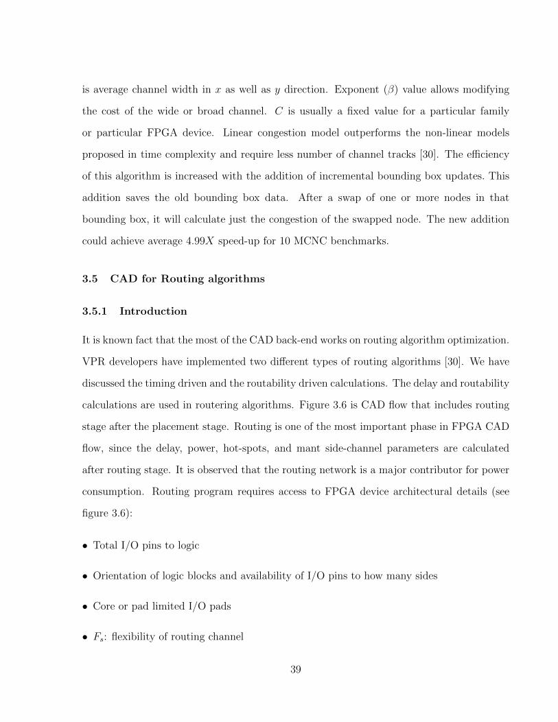
3.4 Linear congestion . . . . . . . . . . . . . . . . . . . . . . . . . . . . . . . . . 37
3.5 CAD for Routing algorithms . . . . . . . . . . . . . . . . . . . . . . . . . . . 39
3.5.1 Introduction . . . . . . . . . . . . . . . . . . . . . . . . . . . . . . . . 39
3.6 Delay measurement techniques . . . . . . . . . . . . . . . . . . . . . . . . . . 42
3.7 Motivation for optimization in floor planning for thermo-power aware CAD . 46
3.8 Summary . . . . . . . . . . . . . . . . . . . . . . . . . . . . . . . . . . . . . 46
CHAPTER 4 THERMAL-AWARE FPGA PLACEMENT . . . . . . . . . . . . . . 48
4.1 Introduction . . . . . . . . . . . . . . . . . . . . . . . . . . . . . . . . . . . . 48
4.2 Various thermal aware design methods for FPGAs . . . . . . . . . . . . . . . 48
4.2.1 Heat-sink based cooling . . . . . . . . . . . . . . . . . . . . . . . . . 49
4.2.2 Xilinx Power Analyzer for heat sink performance . . . . . . . . . . . 52
4.3 Thermal gradient in integrated circuits . . . . . . . . . . . . . . . . . . . . . 54
4.4 Modified Simulated Annealing cost function . . . . . . . . . . . . . . . . . . 56
4.4.1 Temperature Flattening . . . . . . . . . . . . . . . . . . . . . . . . . 56
4.4.2 Thermal benchmarking . . . . . . . . . . . . . . . . . . . . . . . . . . 58
4.5 Custom Thermal-Aware Flow . . . . . . . . . . . . . . . . . . . . . . . . . . 60
4.6 Result analysis . . . . . . . . . . . . . . . . . . . . . . . . . . . . . . . . . . 61
CHAPTER 5 CONCLUSION AND FUTURE WORK . . . . . . . . . . . . . . . . 65
5.1 Conclusion . . . . . . . . . . . . . . . . . . . . . . . . . . . . . . . . . . . . . 65
5.2 Future work . . . . . . . . . . . . . . . . . . . . . . . . . . . . . . . . . . . . 65
APPENDIX A . . . . . . . . . . . . . . . . . . . . . . . . . . . . . . . . . . . . . . 67
REFERENCES . . . . . . . . . . . . . . . . . . . . . . . . . . . . . . . . . . . . . . . 68
BIOGRAPHICAL SKETCH . . . . . . . . . . . . . . . . . . . . . . . . . . . . . . . . 72
CURRICULUM VITAE
viii

LIST OF FIGURES
1.1 Basic Logic Element . . . . . . . . . . . . . . . . . . . . . . . . . . . . . . . . . 2
1.2 Schematic representation of a generic island style FPGA . . . . . . . . . . . . . 3
1.3 Modern FPGA Architecture . . . . . . . . . . . . . . . . . . . . . . . . . . . . . 7
2.1 CMOS Ciruit for dynamic power consumption analysis [1] . . . . . . . . . . . . 11
2.2 Monte Carlo simulation flow [2] . . . . . . . . . . . . . . . . . . . . . . . . . . . 15
2.3 ACE Modified Algorithm [3] . . . . . . . . . . . . . . . . . . . . . . . . . . . . . 19
2.4 Simplification phases for reducing time complexity in ACE algorithm [3] . . . . 20
2.5 FPGA-SPICE CAD tool flow [4] . . . . . . . . . . . . . . . . . . . . . . . . . . 22
2.6 Grid level and Component level simulation testbench blocks in FPGA SPICE [4] 23
2.7 Effect of temperature on leakage current in CMOS devices [5] . . . . . . . . . . 24
2.8 Variation in power consumption and temperature with activities at input [3] . . 25
3.1 Combining two BLEs for reducing total inputs to a cluster. . . . . . . . . . . . . 30
3.2 VPack algorithm pseudo-code . . . . . . . . . . . . . . . . . . . . . . . . . . . . 32
3.3 Pseudo-code for simulated annealing based placer . . . . . . . . . . . . . . . . . 34
3.4 VPR CAD tool flow [6] . . . . . . . . . . . . . . . . . . . . . . . . . . . . . . . . 37
3.5 VPR assumed FPGA model [7] . . . . . . . . . . . . . . . . . . . . . . . . . . . 38
3.6 Position of router in VPR CAD . . . . . . . . . . . . . . . . . . . . . . . . . . . 40
3.7 Traditional router methodologies of expansion and sinking wires . . . . . . . . . 41
3.8 VPR router methodologies of expansion and sinking wires . . . . . . . . . . . . 42
3.9 Circuit representation of routing switches and routing network . . . . . . . . . . 43
3.10 Intuitive example to solve for Elmore delay for RC routing network . . . . . . . 44
3.11 Complete flow diagram of Versatile Placement and Routing evaluation . . . . . 45
4.1 Heat-sink structure for stacked or 2D FPGAs . . . . . . . . . . . . . . . . . . . 50
4.2 Variation of Tj with various VDD for airflow rates in Linear Feet per Meters . . . 54
4.3 Variation of Tj with different size and different quality heat-sinks . . . . . . . . 55
4.4 Illustration of the temperature flattening flow during placement. . . . . . . . . . 58
4.5 Placement of high power blocks from the golden run (a) and the location of thesame blocks in the custom run (b) with the new power numbers. The change inthe power values is due to the change in dynamic and leakage temperature values.Note that the scale for figure b is much smaller compared to a. . . . . . . . . . . 60
ix

4.6 Comparison of the heatmaps for alu4 showing the reference VPR design (a)against the one with the worst performance but the best thermal profile forγ = 0.5 (b). One of the several clusters of hot spots is circled in (a) for clar-ity. All temperatures shown are in Kelvin. . . . . . . . . . . . . . . . . . . . . . 61
4.7 The best and worst delay designs generated for each benchmark. The best(mindelay) design corresponds to the reference design using VPR default flow and theworst(max delay) design is the one at the power threshold that includes around20% of high power blocks for each benchmark. . . . . . . . . . . . . . . . . . . . 62
4.8 Normalized critical path delays versus the high power block spreading factor γ.The best design is obtained for γ = 0.2, 0.875 and the worst is at γ = 0.5 forthe custom cost function. The ratio of delays of custom run by golden run isrepresented by the upper plot . . . . . . . . . . . . . . . . . . . . . . . . . . . . 63
x

LIST OF TABLES
2.1 Performance comparison of activity estimators [3] . . . . . . . . . . . . . . . . . 18
2.2 Performance comparison of activity estimators [8] . . . . . . . . . . . . . . . . . 21
2.3 Performance comparison of activity estimators [3] [8] . . . . . . . . . . . . . . . 23
4.1 Vendor Recommendations for FPGA Cooling Solutions . . . . . . . . . . . . . . 52
4.2 Heatsink selection for benchmarks tested. . . . . . . . . . . . . . . . . . . . . . . 52
4.3 Thermal Resistances of commercial heatsinks . . . . . . . . . . . . . . . . . . . 53
4.4 Vendor Recommendations for heatsinks . . . . . . . . . . . . . . . . . . . . . . . 53
4.5 Thermal flow simulation results . . . . . . . . . . . . . . . . . . . . . . . . . . . 64
A.1 Benchmark Characteristics. . . . . . . . . . . . . . . . . . . . . . . . . . . . . . 67
xi

CHAPTER 1
INTRODUCTION
Gordon Moore made an observation in 1965 about the density of transistors in integrated
circuits (ICs). Moore's law states that the number of transistors in an IC doubles after 18
months. Moore's observation proved accurate for many decades. NVIDIA GP100 Pascal
GPU contains more than 15 billion transistors. One way to invest this many transistors is
multi-core processing units. Multi-core processing increases the performance of the appli-
cation. However, if we look at the trend of cores added, it is clear that the gain in terms
of performance by adding more number of cores is diminishing after a point. Additional
cores require adjustment to the existing software and OS. But simply adding more cores
is at times not very useful and sometimes wastes power. Field Programmable Gate Array
(FPGA) is the reconfigurable device which contains uncommitted silicon. FPGAs are tra-
ditionally developed for prototyping or functional testing the ASIC designs before sending
out to foundries. Advancements in FPGA architectures and CAD tools over the years have
made FPGA devices as preferred architecture for many search engines as well as primary
machines to run machine learning algorithms.
1.1 Field Programmable Gate Arrays (FPGAs)
The island style FPGA is an uncommitted pre-fabricated silicon semiconductor device formed
of uniform structures of arrays in island style Logic Blocks (LBs) or Configurable Logic Blocks
(CLBs)[9]. Each CLB consists of a set of Basic Logic Elements (BLEs) (see figure 1.1). Each
BLE has Look Up Table (LUT), D-Flip Flop, and a multiplexer to select the output out of
the BLE. The most common architecture of an FPGA is shown in figure 1.2. This common
island style FPGA architecture (see figure 1.2) is composed of three fundamental blocks,
namely :
1

Figure 1.1. Basic Logic Element
• Reconfigurable programmable logic blocks
• Internal wire routing network, programmable switch and connection boxes
• Input and Output pads that connect internal routing network to external connections
1.1.1 Logic Blocks
A logic block or Configurable logic block comprises of a number of BLEs (see figure 1.1).
If we zoom into each BLE, it will have k-LUT. In this notation, k is a number of inputs to
LUT. A k input LUT will require 2k SRAM bits for configuration. k-LUT can implement any
k-input logic function. The latest Xilinx series 7 FPGAs consists of memory slice (SLICEM)
and logic slice (SLICEL). Latest FPGAs include typically 4 to 10 Basic Logic Elements
in one cluster. There are fracturable BLE architectures proposed that contains possible
combinations and mixture of number of inputs. Logic block category also include memory,
Arithmatic and Logic Unit, DSPs, etc.
2

Figure 1.2. Schematic representation of a generic island style FPGA
1.1.2 Routing architecture
An island-style FPGA architecture as shown in figure 1.2 depicts the island of configurable
logic blocks in a sea of routing interconnect. Unified 2D grid array of CLBs are connected
by configurable routing metal wires. Network also connects primary inputs and outputs
to logic blocks. Re-programmability in pre-fabricated wiring segments comes from switch
and connection box connections. Typical routing network occupies 8090% of FPGA area.
Connection boxes (CB) route the output of LUTs to a switch box (SB). Limited number
of wiring tracks and SB connections pose the network congestion problem. The term Fc is
associated with connection box flexibility. It denotes the number of connections from the
logic block to route. Similarly, Fs is the flexibility of switch box. It is the possible connections
available inside SB for an input pin to route. Detailed discussion on routing algorithm and
architecture is provided in chapter 4.
3

1.2 FPGA Physical Design Flow
In this section we briefly describe the mapping process for FPGAs. There are following 5
stages involved in FPGA physical design flow.
• Design entry
• Technology mapping
• Physical placement
• Routing
• Configuration bit-stream generation
1.2.1 Design Entry
This is the first step in the process of mapping design on the FPGA device (figure 1.3
describes heterogeneous modern FPGA architecture). The hardware description language
depicts the circuit description design specification. There are various synthesis tools available
for entering the design. Most of the CAD tools supports Verilog or VHDL programs for
describing Register-Transfer Level (RTL). There are other ways to map the design such as,
adding schematics (.sch), net-list (.ngc, .edif) and microprocessors (.xmp) directly to the
project. Various custom or pre-defined IPs can be included in this method. For the synthesis
of the entered design, synthesis technology (for example XST) converts entered RTL or IPs
to a netlist that will be used for implementation. Technology and RTL schematics provide
information to the user about synthesized design. Synthesis tool parses the HDL code and
checks for the syntax. There are various types of special functions are available to used in
a HDL program like keep, case, OPT LEVEL, etc. for synthesizing constraints. Synthesis
tool can detect finite state machines in the program and apply the encoding style in order to
4

optimize the area and boost the speed. Macro generation, flip-flop re-timing, partitioning,
incremental synthesis, re synthesis, etc. are the schemes used by synthesis tool for FPGA
optimization.
1.2.2 Technology Mapping
FPGA architecture includes unified array of logic blocks. After translating the design in
the form of gate level netlist, technology mapping packs the design in the form of K input
Look Up Tables (K-LUTs) and combine LUTs to form Configurable Logic Blocks (CLBs).
Generally technology mapper optimizes for area utilized and minimum delay. Translate phase
takes the design constraint file (.ucf or .xdc) and relates it with the netlist. This translation
will produce native generic database (.ngd). Map deals with extracting the input-output
buffers (IOB) and CLBs defined in the .ngd file. Map produces native circuit description
file (.ncd). There are different types of algorithms for various optimization goals. Network
flow, bin packing algorithms are among the popular algorithms for technology mapping.
1.2.3 Physical Placement
Each block in the Configurable Logic Block (CLB) level netlist will be assigned a physical
location on FPGA device. The assignment of CLBs to unique x, y location process is called
as Physical Placement. Placement algorithm place the co-related blocks closer in order to
reduce delay and interconnection complexity.
1.2.4 Routing
Physical placement assigns a x, y location to each of the logic block in netlist. Figure 1.2
depicts the interconnection network connecting Logic Blocks through connection box and
switch box. Detailed routing architecture and algorithms are explained in chapter 3. Routing
algorithm need to consider congestion in network, critical path, and advance issues include
5

not only but false path, cross talk, power optimization. Multiple parameters such as the
architecture of routing network, logic block geometrical orientation, flexibility of switch and
connection box has an effect on performance of routing resource utilization and performance.
1.2.5 Configuration bit-stream generation
Bitgen generates a bitstream (.bit) which can configure the SRAM bits in FPGA. After
configuring the FPGA device, there are ways to test and debug the design. ChipScope
software can be used which allows adding debug cores in design. Integrated logic analyzer
(ILA), virtual input output (V IO) software cores make is possible to add probes at nets
which are to be considered for on-chip testing. ILA allows real-time probing and observing
the nets inside the logic.
1.3 Motivation
Growing size of FPGAs and performance hungry applications are draining a lot of power.
CAD tools consider wire-length and area of the chip utilized for the optimization problem.
However many research groups in the industry as well as in academia are now considering
power consumption and temperature of the chip as one of the major metric for optimization.
The problem of power consumption and a tremendous increase in temperature are major
concerns in proposed 3D FPGA designs. Because of which making the CAD tools power
and thermal aware is an open and very demanding field for research.
The key motivation for this research is to reduce the density of the hotspots. Reduction
in junction temperature can justify the purpose. The current research on power and ther-
mal aware designs is moving towards post implementation analysis and employing different
cooling mechanisms. However, this research focuses towards the early stage of the design
flow for thermal and power-aware placement algorithm. To achieve early awareness in CAD
tools for thermal and power-aware designs, it is most essential to obtain accurate simulation
6

Figure 1.3. Modern FPGA Architecture
model for power calculations. FPGA-SPICE [4] creates a hspice model of each of the block
in FPGA architecture. The uniformity in logic blocks and interconnection networks soothes
the process of determining power profile of FPGA. Xilinx Power Estimator (XPE) is a good
way to obtain vector-based or vector-less power numbers though simulating benchmarks.
This research is the demand in industrial as well as military application in FPGAs.
1.4 Research Contributions and Thesis Organization
In order to overcome the device failure due to hotspots and high junction temperature, we
came up with a few methods at different design stages.
7

• We have developed a power and thermal aware placement method. The placement
algorithm implemented in VPR [7] and T-VPack [10] (Versatile Packing Placement
and Routing) uses simulated annealing. We have modified the placement algorithm
(simulated annealing) that consider power as one of the optimization constraint. We
modified the cost function associated with this algorithm with adding extra we studied
the initial placement of the simulated annealing. For accurate results, we then obtained
CLB level power of benchmarks. Activity estimation of nets in design is carried out
with the help of ACE2.0 activity estimator [3].
• We studied heat sink performances with different board sizes and air-flows. The
sweep of airflow rate for different board size and qualities of the heat sink for maxi-
mum junction temperature is carried out. Simulation results shows ineffectiveness of
the active and passive heat-sinks in high performance computational FPGA devices.
The thesis is organized into following chapters:
In chapter 2 we present the brief study of different FPGA architectures and study of power
and temperature associated with components of FPGA.
In chapter 3 we describe different placement algorithms and form a base foundation for
understanding delay and power measurement techniques.
In chapter 4 we outline key research and prior works in FPGA thermal management field.
In chapter 5 we formulate and explain the proposed algorithm for placement scheme. We
also discuss the benchmarks used for capturing results. This section includes in detail study
of accurate power measurement tools, CAD tools used for research and CAD flow.
In chapter 6 we present conclusions, remarks and discuss future scopes of this work in
different dimensions.
8
CHAPTER 2
POWER ESTIMATION IN FPGAS
2.1 Introduction
This chapter describes power consumption and associated power and thermal measurements
in FPGA devices. We present literature and prior work on power analysis in VLSI design as
well as FPGAs. In high performance computing applications, there are two popular choices
when it comes to implementing algorithms on hardware. GPUs (graphical processing units)
are extremely common as they offer small multi-cores that enable extreme parallelism for
a large number of applications. GPUs are marred by their excessive demand for power
consumption. The alternative solution that seems to be emerging is the use of FPGAs.
FPGAs are popular due their low power consumption, low cost, and an ability to pro-
totype a large class of applications. An excessive computation demand is becoming more
and more responsible for rise of the on chip temperature, thermal failures, and is forcing the
design and use of aggressive cooling methods.
In order to attain accurate thermal characterization, it is important to study and under-
stand the mechanism of power dissipation in FPGAs and the the tools that are used for early
estimation and accurate evaluation of power associated with FPGA mapped applications.
We first present the general sources of power in CMOS technology and then present a survey
on literature for power estimation.
2.2 Sources of power
2.2.1 Static (Leakage) power
• PN junction Reverse Bias leakage This leakage is caused due to the leakage current
through reverse biased p-n diode junctions of the transistors. It is the current be-
tween the drain (or source) and the substrate. At the room-temperature this type of
9

leakages are minimum but as at the higher temperature, this leakage current can be
non-negligible.
• Sub-threshold leakage Subthreshold leakage is caused due to the flow of current in
weakly inverted source and drain terminal. The direction of current is from drain to
source hence it is also referred as D-S leakage. The exponential relation in leakage
current and Vth, with very small increase in Vth effects in a reduction in subthreshold
current.
Isub =µCoxW
LVT (2.1)
Where, µ is the electron mobility, Cox is oxide capacitance
• Gate leakage This leakage is due to the current because of low thickness of the oxide and
a tunnel through the gate oxide. Scaling down with the transistors, this type of leakage
is no more negligible. There are ways to reduce the gate leakage viz., not reducing the
oxide thickness below the limit with the process scaling, insulating the gate terminal
with the material of high dielectric constant.
Igate ∝ Weff. (2.2)
2.2.2 Dynamic power
Dynamic power is also called as switching power since it is the power dissipated in charging
and discharging the load capacitance by the CMOS circuit (see figure 2.1).
ic(t) = CLdccdt
(2.3)
Energy dissipation from VDD on every input transition from 2.3
EV DD =
∫ ∞0
iVDD(t)VDDdt = CLVDD
∫ VDD
0
dvC = CLV2DD (2.4)
10

Figure 2.1. CMOS Ciruit for dynamic power consumption analysis [1]
Similar calculations prove that energy stored in load capacitor is half of the energy
dissipated by VDD,
ECload=CLV
2DD
2= EDynamic (2.5)
The remaining half energy is dissipated in switching action (see equation2.5). Power is
integration of energy per unit time.
Pdynamic =CV 2fclk
2(2.6)
From the above equation of dynamic power dissipation, following techniques can be
implemented to reduce Pdynamic:
• Supply voltage has a square relation with Pd. Hence the reduction in supply voltage is
one of the most effective ways to reduce total dynamic power consumption. However,
there is a limit to reduce the supply voltage since it has a direct impact on circuit
performance and highest operating frequency. Chow et al. [11] proposes multiple
power supplies and scaling of the voltages as an alternative to a reduction in supply
voltage.
11

• Operating frequency and the switching activities have a direct impact on dynamic power
dissipation. Using pipe-lined architectures, implementing multiple clock domains, fre-
quency scaling is few of the successful techniques implemented in order to reduce
switching component. However, latest technologies are capable of working at tremen-
dously high clock frequencies for performance. Hence the demand for dynamic power
consumption is increasing.
• The last component in equation 2.6 is Cload. Cload is an additive effect of output capaci-
tance and self-capacitance of the CMOS devices in the circuits. This component also
includes wire capacitances. Hence optimally sizing the transistors and minimizing wire
capacitances will help in reducing overall Cload.
2.2.3 Short circuit power
Rise and fall at the input of a transistor cannot be a sharp edge. Input slew rate is responsible
for short circuit current. During the transition from low to high or high to low at the input
of the CMOS logic, it is possible that both pull up and pull down the network is active
which creates a path for current from VDD to Gnd. This conduction of current from supply
to ground is undesirable and called short circuit current.
ESC = VDDIpmostSC (2.7)
PSC = tSCVDDIpmosfclk (2.8)
This type of leakage can be minimized linearly by lowering the VDD. Also, designing less
sensitive output rise and fall time with respect to input slew rate will operate either PUN
or PDN at one instance which will avoid the short circuit path.
12

In early phases of technology scaling till 130 nm, dynamic power dominated the total
power dissipation. Moving towards low node process technologies, static leakage has played
a dominant role. The increase in static power dissipation component is due to lowering of the
channel width and overall transistor sizes. This phenomenon increases the leakage current
since the threshold voltage is continuously lowering with the scaling down of transistor sizing.
In this section, we focus on academic tools for estimation of power measurement in FPGAs.
We will also present prior works done in this area of research.
Power estimation performed at coarse grain architecture is less accurate than the estimation
performed fine grain architectures. Also, as we go down in the levels of abstraction, it
becomes increasingly difficult as well as computationally inefficient to perform accurate power
estimation. Power analysis and estimation can be sub-divided into two categories:
1. Simulation based power analysis: In this type of technique for power analysis,
Simulation Program with Integrated Circuit Emphasis (SPICE) based simulations are
used for estimation. Since SPICE simulations are performed at the device level, these
estimations have higher confidence and are accurate. It stimulates the dynamic be-
havior at the transistor level and demands SPICE netlist of components in the device.
High granularity and huge computation for large FPGAs makes simulation based anal-
ysis very time-consuming. To boost the execution time of the SPICE simulations, often
a transistor-level netlists will be combined to form high-level abstraction units. In the
case of FPGAs, a technology mapped CLB level netlist will always perform faster than
Basic Logic Element (BLE) or Logic Gates level netlist. However, these simulations
are highly dependent on quality and quantity if inputs to the circuit. Simulation-based
estimation procedure can be described as below:
(a) Since inputs pattern has a major impact on simulation results, decide on a number
of input vectors and simulate circuit under test with those patterns.
13

(b) In order to obtain an accurate estimation for dynamic power, it is important
to accurately model the switching behaviour of nets involved in a design. The
probability that the net will flip from a low to a high or vice versa is estimated
using an activity estimator block.
(c) Table based or statistical model based leakage power calculation model is used for
estimating the leakage power. The leakage power is related to temperature and
the sizing of the device and is easily modeled by a statistical model.
(d) Total power will include the dynamic, leakage and routing (global as well as local)
powers.
The major drawback of the simulation-based power estimation technique is set of in-
put pattern vectors. A bad choice of a set of vectors will have a high error in total
power measurement. A random vector generator is proposed in order to estimate most
accurate power profile. The algorithm comes from decision making and risks impact
theory. It is a mathematical model applicable to many such problems, in which out-
come depends on a large set of inputs. The algorithm starts with the random set
of values and calculates the results. The process of random generation of vectors for
simulations can perform many thousand iterations till it encounters a terminating con-
dition. Every iteration of the algorithm calculates mean and variance of the estimated
outcome. Loop condition determines confidence in the output and jumps to a termina-
tion or iterate with another random vector. The first publication of the above Monte
Carlo based method was published in 1940. Later on, Monte Carlo method [2] (see
figure 2.2) was used for solving a wide range of problems in computer programming
world. Simulation-based power estimation requires a set of input vectors for SPICE
simulation.
14

Figure 2.2. Monte Carlo simulation flow [2]
15

2. Probability based estimation: It has been studied in the past that the simulation
based estimation techniques are very time to consuming since SPICE execution for
large integrated circuit design is computationally expensive. Most research in the past
that is related to fast simulations and power estimation techniques publish about the
probabilistic estimation of power. Each net or wire in the circuit has static probability
P1(x) which can be defined as the probability that the value of net x will stick to logic
one. Static probability value has an importance in measuring leakage power since it is a
direct measure of how long a transistor can hold same logic value. The dynamic power
of a circuit is a direct function of switching activity of a net. Hence, the probability
of switching the steady state value on net from a logic high to logic low or low to high
during one clock cycle is defined as switching probability Ps(x). Notation As(x) of any
net x can be explained as an average number of times a net value transitions from low
to high or otherwise before attaining a steady state value and it is called as transition
density. It is clear that activity of the net is required for achieving accurate power
characteristics since dynamic power dissipation depends on the switching activity.
Probability based estimation techniques are also called as vector-less activity estimation
techniques. These approaches are computationally faster than the simulation based
estimations. Few probabilistic estimation methods ignore the temporal and spacial
correlation between two or more nets in same circuits. In the case of re-convergent
fan-out nets, we observe special correlation. In sequential feedback loops from the
output of the flip-flops to input forming network, we observe temporal correlation.
Lamoureux et al. [3] illustrated the error percentage by ignoring correlations. Ignoring
special correlation may result in 8 to 120 percent error and 15 to 50 percent possible
error with the ignoring of temporal correlations. There are techniques which consider
temporal as well as spacial correlations. [12] [13].
16

• Measuring accuracy of the activity estimator
There are a number of activity estimation tools available. Accuracy and execution
time for calculating activity estimate are the empirical quantities. Three metrics
are used for evaluating the accuracy of the activity estimator. The average relative
error is the average of the error in estimated activity of every wire in a design. It
can be calculated as follows (see equation 2.9):
Average relative error =
∑n∈circuit
Asest (n)−Assim (n)
Assim (n)
|circuit|(2.9)
Where, Asest is the estimated activity of net and Assim is the simulated activity
of net. Another evaluation measure is r2 correlation. It measures the co-ordinal
relationship between estimated and simulated values of activities. Formula for r2
correlation is:
r2 =ss2xy
ssxxssyy(2.10)
Here, ss denotes sum of squared values. The values are calculated co-ordinally
for xi which is estimated activity of net and yi is simulated activity in net space.
For each data point, xi (the estimated activity) and yi (simulated activity) is
considered. Desired value of term r2 is one since, when r2 is equal to one, it
describes the exact match in simulated and estimated activity values i.e. 100%
accurate estimation. Third evaluation metric is activity ratio. It is simply the
ratio of the summation of the estimated activities to simulated activities. Activity
ratio one describes most accurate estimation. The formula can be expressed in
below equation (see equation 2.11):
Activity ratio =
∑n∈circuitAsest(n)∑n∈circuitAssim(n)
(2.11)
Where, Asest , Assim is the estimated activity of net and the simulated activity of
net respectively.
17

Table 2.1. Performance comparison of activity estimators [3]Simulation Sis1.2 ACE1.0Comb Seq Comb Seq Comb Seq
Activity Ratio 1 1 1.17 1.40 1.21 2.37Avg error 0 0 0.02 0.09 0.07 0.08r2 1 1 0.88 0.72 0.89 0.47Runtime Sec 122 191 ∞ ∞ 31 108
2.2.4 ACE 2.0 Activity estimation tool
Above three parameters serve as metrics to measures for the accuracy of an estimator.
Lamoureux et al. [3] who proposed ACE 2.0 activity estimator compare the results of
two estimators shown in the table (see table 2.1). The author states that even for the
smallest sequential circuits, because of the insufficient storage Sis 1.2 [8] is unable to produce
estimations in finite time. Required execution time grows exponentially with the number of
inputs to the sequential elements. One observation to be made is that even though tools are
not able to produce estimates in finite time for many sequential circuits, the estimates for
combinational logic are relatively accurate and the speed of execution is better compared to
sequential circuits. To overcome the speed of estimation for sequential circuits, the author
has proposed a new ACE-2.0 [3] estimator for activity. Since Sis-1.0 is exponentially slow
with increasing number of inputs and ACE-1.0 is not very accurate, power aware CAD
tools demands fast and accurate estimator. ACE-2.0 tries to demonstrate both speed and
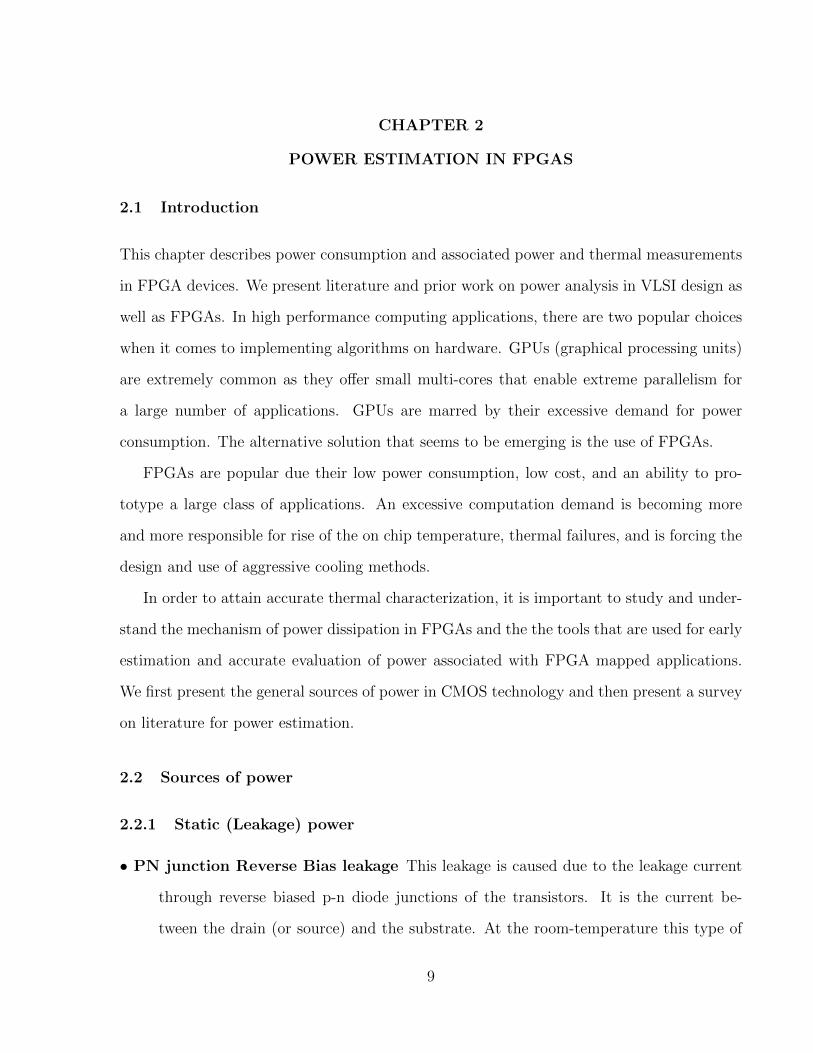
accuracy. New proposed algorithm works in three phases as detailed in figure 2.3.
Static power and switching power are the two components that are most important in
the calculation of power consumption. As seen in results earlier from table 2.1, sequential
feedback takes the longest time for execution. Usually, circuits with large number of flip-flops
are error prone in the calculation of probabilities. The new ACE tool works in three phases
(see figure 2.3). The first phase works on simplifying the calculations for a reduction in exe-
cution or simulation time. As discussed, sequential addition is one of the major contributors
18
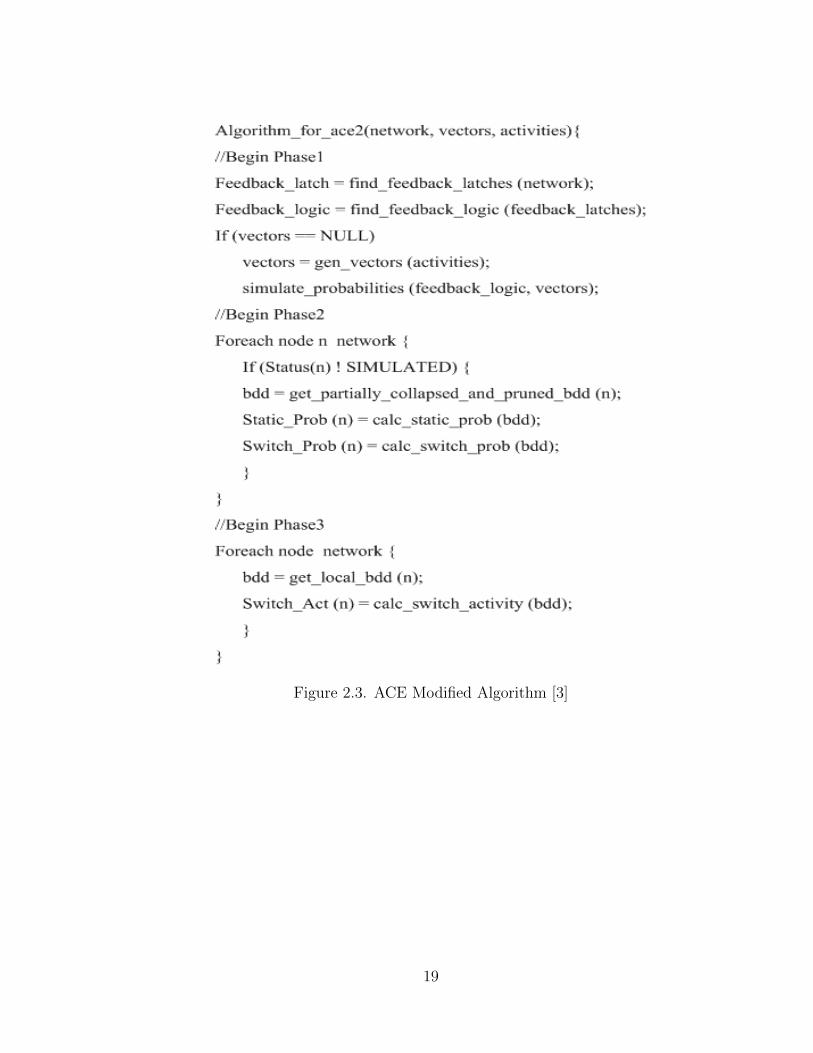
Figure 2.3. ACE Modified Algorithm [3]
19
Figure 2.4. Simplification phases for reducing time complexity in ACE algorithm [3]
for extra simulation time. This phase ignores the sequential feedback and then simulates
remaining logic. The assumption made here is that logic present in simulating sequential
circuits is very small compared to the remaining logic. Another method that is implemented
for reducing time complexity is a simulation of the switching probability instead of switch-
ing activities. A net can switch more than once during one clock cycle before reaching a
steady state value. But, observing the last steady state value on the wire after complete
cycle determines the switching probability. It is computationally cheaper to simulate for
probabilities than monitoring every single change occurred on every wire. We will call the
first simplification as simplify1 and second one as simplify2. (see figure 2.4)
In the phase2 of the algorithm, it calculates the ignored and remaining switching prob-
abilities in the sequential feedback loops. Lag-one model is used to calculate the switching
probabilities. For faster simulations, the gate level network is collapsed in the smaller net-
work. Binary Decision Diagram and Partial collapsing methodologies are used for forming
collapsed network. The partial Collapsing method can be understood in the figure 2.4. Since
20

Table 2.2. Performance comparison of activity estimators [8]ACE 2.0 Power Model CAD
Avg r2 Act rat Rel err Runtime Diff P saveseq 0.97 0.97 0.03 2.3 −0.1 8.8comb 0.86 1 0.02 25.9 0.6 14
it is possible that collapsed network will include special correlations, the activities estimated
will be un-precise. Collapsing into smaller networks will assure more accuracy. However, the
trade off with speed of simulation and accuracy is the key consideration. In the BDD prun-
ing method, a pruning threshold probability (minimum sw prob) is decided. Any probability
below the pruning threshold will not be considered in the calculation. Such sub-trees will be
removed and assigned P s=0 for the parent node of sub-tree. The algorithm is executed in
a recursive manner starting from root to the leaf of the tree. Phase3 of this algorithm works
on glitches. Many optimization tools ignore the propagation delay or the race conditions.
Effect propagation of glitches is studied, and using the lag-model, the existing algorithm is
modified for betterment in the calculation of switching probabilities. Results shown in table
2.2 describe the ACE-2 accuracy and performance.
2.2.5 FPGA SPICE for power measurement
Probability based power estimators are less accurate and not very flexible to architectural
modifications in the FPGA model. FPGA SPICE tool developed by Xifan Tang and Giovanni
De Micheli in 2015 [4] outperforms existing VersaPower [10] tool built inside VPR engine
[7]. This specific tool is built on top of the VTR suite. In the SPICE flow (see figure
2.5), the VersaPower [10] is replaced by the FPGA-SPICE [4] engine and it outputs the
SPICE level netlist to HSPICE simulator. This simulator also takes pre-built spice models
for components in FPGA. The tool has an ability to generate the netlist at three levels of
abstractions. With reference to an FPGA architecture, a full-chip, or a grid, or a component
level netlist can be generated. Full chip level netlist will require large memory storage to
21

Figure 2.5. FPGA-SPICE CAD tool flow [4]
execute. SPICE tool generates a transistor level netlist of components present in the FPGA
architecture. Granularity of SPICE simulation models is illustrated in (figure 2.6).
SPICE performs better for power calculations. It predicts the power numbers that con-
sider parasitic delays and activities as well. FPGA SPICE estimated power values are less
time complex and results can be analyzed from (table 2.3). In table 2.3, benchmark s298 is
evaluated for 3 different types process technologies. Chip level power estimation takes the
maximum time and it requires maximum memory compared to grid and component level
SPICE simulations.
22

Figure 2.6. Grid level and Component level simulation testbench blocks in FPGA SPICE [4]
Table 2.3. Performance comparison of activity estimators [3] [8]s298 runtime in min memory in Mb Power in mW
process tech 22nm 45nm 180nm 22nm 45nm 180nm 22nm 45nm 180nmChip 129.48 106.15 102.56 4780 4827 4306 1.56 4.13 15.63grid 10.27 9.82 8.25 768 768 825 1.41 3.37 18.03component 7.42 6.97 6.23 589 584 621 1.45 3.21 17.57
23

Figure 2.7. Effect of temperature on leakage current in CMOS devices [5]
2.3 Power and Thermal modeling with CAD
Total power consumption in VLSI circuits has two major components: dynamic power and
static power. We have seen the detailed description for both power dissipation components
in the previous section. Static power consumption is mainly a contribution of leakage cur-
rent (gate and sub-threshold). The leakage current and temperature relation are plotted in
figure 2.7. Looking at the equation of dynamic power dissipation (equation 2.6), the power
dissipation is not strongly related to temperature.However, static dissipation is related to
sub-threshold and gate leakage. Which directly are functions of temperatures (2.7).
From figures (2.8 and 2.7) it can be clearly seen the direct relationship in temperature and
power consumption. Pdyn is not exponential with temperature, but since higher frequency
components are associated with dynamic power consumption and same leads to increase in
junction temperature as well. (see equation 2.12)
Tj = Tamb + Ptotalθja (2.12)
24

Figure 2.8. Variation in power consumption and temperature with activities at input [3]
Here, Tj is the junction temperature, Tamb is ambient temperature, Ptotal is total power
consumption, and θja is junction to ambient thermal resistance.
The HotSpot thermal simulator [14] is popular for its use in block level thermal simu-
lations. Many CPU and computer architecture designing community utilizes HotSpot tool.
Re-configurability for different architectures is one of the advantages of HostSpot technology.
In the thermal model, a layer of an active semiconductor is divided into a number of units.
Each newly formed unit can be considered as a node. Each node has the thermal resistance
in vertical and horizontal direction. It accounts for lateral heat spreading complexity. Exist-
ing thermal simulators have the ability to simulate the system or package level. Since with
the high active silicon power consumption, more detailed and accurate simulation model was
needed. HotSpot takes reference from Runge-Kutta RC circuits in the fourth differential
order [15]. The differential equation solver is self-adaptive for different size of units. SESC-
Therm [16] is another thermal simulation model works on the principal of Finite Difference
Model (FDM) [17]. The principal is dividing the problem into multiple segments. Each
segment is evaluated separately. Solving a differential equation for the very large segment is
time expensive. However, FDM complexity exists in analyzing thermal conduction over the
25

segments. The core of this algorithm is similar to HotSpot. Each node is characterized by
source, sink, thermal resistance, and capacitance. Characteristics updates with the change
in temperature and on boundary conditions. Steady state power blurring algorithm [18] [19]
has an ability to solve thermal models using image processing tools. The methodology imple-
ments a filter or so-called thermal mast which convolve the power value matrix. Simulation
of the thermal mask is look up the table based implementation for reducing execution time.
2.3.1 3D-ICE thermal simulation tool
We use the 3D-ICE thermal simulator [20] for generating temperature values for FPGA.
This tool is developed by Embedded Systems Laboratory (ESL) research group in EPFL.
The primary contribution of 3D-ICE tool is to propose a compact transient thermal model
(CTTM) mainly for micro or macro fluid cooling. The modeling of FDA is not in in the
scope of the thesis. The software is built in C programming. It uses Flex, Bison tools for
computation and runs on gcc engine. Tool interface to the user takes physical parameters
and description of the IC layer(s): called stack description file, floorplan file which includes
power dissipation for each logic unit, and time of simulation.
VPR [7] and FPGA SPICE [4] tools generated power distribution is parsed. From the
architectural input provided to 3DICE [20], it generates a thermal grid. The output file
(thermal profile.tmp) will dump the temperature value for logic elements. Visual plotting
can be performed with the help of MATLAB tools.
An example FPGA stack file is described below:
material SILICON:
thermal conductivity 1.30e-4 ;
volumetric heat capacity 1.628e-12 ;
material BEOL :
26

thermal conductivity 2.25e-6 ;
volumetric heat capacity 2.175e-12 ;
top heat sink :
heat transfer coefficient 1.0e-7 ;
temperature 300 ;
dimensions :
chip length 12000, width 12000 ;
cell length 100, width 100 ;
layer PCB :
height 10 ;
material BEOL ;
die BOTTOM IC :
layer 10 BEOL ;
source 2 SILICON ;
layer 100 SILICON ;
stack:
die FPGA DIE 1 BOTTOM IC floorplan ”./alu4 golden.dat.flp”;
layer CONN TO PCB PCB ;
solver:
steady ;
initial temperature 300.0 ;
output:
Tmap ( FPGA DIE 1, ”alu4 golden.tmp”, final ) ;
27

2.4 Summary
In this section, we discussed the main sources of power dissipation in integrated circuits and
FPGAs. We also looked at the simulation based and probability based power estimation
techniques. We the concluded that simulation-based power estimation techniques are more
accurate than probability based power estimations. Power consumption is dependent on the
activity associated with the nets in a design. The modified ACE activity estimation tool
performs better than Sis and ACE 1.0 version. We will use the ACE2 tool in the thermal
and power aware CAD flow for FPGAs. We have described the relation between power
and temperature in circuits. Then we have described different thermal models available.
Comparing the performance and accuracy of various models, 3D ICE thermal simulation
tool is easy to use for stacked and 2D FPGAs.
28

CHAPTER 3
CAD FOR PLACEMENT AND ROUTING ALGORITHMS
3.1 Introduction
We have discussed the island style architecture of FPGAs and typical FPGA design flow
in section 1.2. The FPGAs will be programmed with the binary stream (bit-stream) which
configures the hundreds of thousand to million number of programmable switches to connect
to form a routing network. To perform this kind of programmability, an engineer need to
look into the state of every switch and connection configuration. If this was done manually,
implementing small design of hundred equivalent gates will take an enormous amount of
time. We looked into the FPGA implementation flow, in that an engineer writes RT-Level
program in HDL and XST then implementation tools (Computer Aided Design tools) take
care of generating configurations of millions of the connections and routes. However, the
researchers have delved into the problem of the most efficient and optimum algorithm for
placing, routing, and packing. After extensive research on architecture (value of K, N , I)
now most of the commercial FPGA companies are following a common trend of architecture.
The CAD tools are now aware of real time (transient) speed and area efficiency. The focus
of the CAD tools is now making the design power and thermal aware at the implementation
phase or even earlier than that [21] [22]. In this section, we will look in the FPGA flow in
detail and CAD tools perspective for implementing each if the stage in the flow.
3.2 Packing: VPack for logic block packing
Figure 3.1 explains the basic logic element (BLE) and formation of a cluster of multiple
BLEs [7]. The total input to single look-up table (LUT) is denoted by k. Each cluster
will be consisting of total N BLEs. I number of inputs wires to cluster inputs which further
propagate to BLEs inside the cluster. Mclk is defined for a number of clock inputs to a cluster.
29
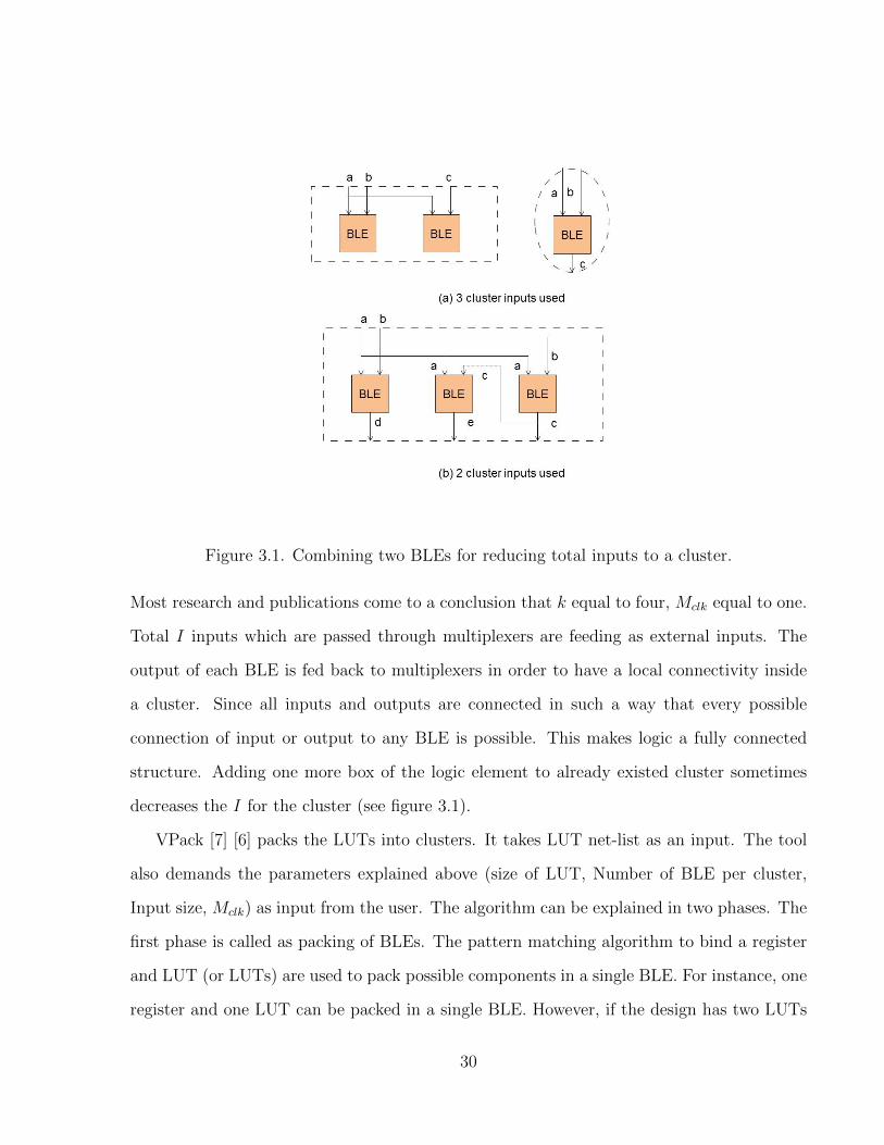
Figure 3.1. Combining two BLEs for reducing total inputs to a cluster.
Most research and publications come to a conclusion that k equal to four, Mclk equal to one.
Total I inputs which are passed through multiplexers are feeding as external inputs. The
output of each BLE is fed back to multiplexers in order to have a local connectivity inside
a cluster. Since all inputs and outputs are connected in such a way that every possible
connection of input or output to any BLE is possible. This makes logic a fully connected
structure. Adding one more box of the logic element to already existed cluster sometimes
decreases the I for the cluster (see figure 3.1).
VPack [7] [6] packs the LUTs into clusters. It takes LUT net-list as an input. The tool
also demands the parameters explained above (size of LUT, Number of BLE per cluster,
Input size, Mclk) as input from the user. The algorithm can be explained in two phases. The
first phase is called as packing of BLEs. The pattern matching algorithm to bind a register
and LUT (or LUTs) are used to pack possible components in a single BLE. For instance, one
register and one LUT can be packed in a single BLE. However, if the design has two LUTs
30

and one register then it will be packed in two separate BLEs. One BLE will be consisting of
a register and LUT. The other BLE will include a LUT. The second phase works on packing
the newly formed BLEs into the clusters. There are couples of optimization goals tied with
this process. First is to minimize the number of logic clusters needed. This can be stated in
a different way as to utilize all used cluster to maximum capacity (N). However, the FPGA
routing network connects the cluster globally. As we have discussed earlier in section 3.2,
I inputs are external to a cluster which potentially are the outputs of other cluster or the
same cluster. Optimizing for a minimum number of cluster inputs (I) will hugely reduce
the routing complexity. The pseudo code is explained in the figure 3.2. To form a cluster,
there are a few filters and conditions required. The maximum basic logic elements (BLEs)
cannot be more than N . The maximum number of different clock sources incoming to a
cluster cannot be more than Mclk. The total number of inputs to a cluster cannot be more
than I. Phase two of packing starts with a greedy implementation of packing of BLEs into
the clusters. If the greedy algorithm is unable to fill a cluster to its capacity, then a hill
climb implementation is used to utilize maximum of the cluster. Initially, a BLE is selected
such that it is not yet clustered (i.e. un-clustered). If there exist more than one such BLE,
then the one with maximum used input is selected. This ensures that BLE will utilize most
of the (I) inputs appearing at the cluster. The attraction of a BLE to a cluster is directly
proportional to a number of inputs outputs BLE have common with cluster (equation 3.1).
After the greedy and hill climb, high attraction BLEs will pack to clusters.
Attraction = [ inputs and outputs(BLE) ∩ inputs and outputs(C) ] (3.1)
In phase2 i.e. adding such BLE to cluster so that input set to the cluster does not grow
us is a critical phase. That BLE will be added which has least ∆BLE.
31

Figure 3.2. VPack algorithm pseudo-code
3.3 Placement
Placement stage in the FPGA CAD flow places logic blocks within a physical device. Op-
timum placement algorithm will have different optimization goals depending on the appli-
cation. Wire length driven placement optimizes for minimum distance and minimum wire
required in global as well as local routing network. It packs and places the design in a dense
manner and ensures dependent blocks are placed closer. Timing driven placer places the
blocks considering maximum frequency and circuit speed. Min-cut placer will divide the
number of logic blocks into two or more partitions such that the number of nets or wires
crossing the partition are minimized. Analytical placement algorithm [23] solves constraint-
based equations to minimize the wire length. It works with co-ordinates and geometrical
equations to solve objective function. We will discuss Simulated Annealing algorithm in
detail.
32

3.3.1 Simulated Annealing
In the year 1930, the traveling salesman problem (TSP) was presented which aims of cal-
culating the optimum tour for a set of multiple locations. Every location should be visited
and the tour ends at the starting point. The nearest neighbor approach could not result in
optimum path tour. The problem is known as non-deterministic in polynomial time com-
plete problem (NP-Complete). The difficulty of this problem solution grows when the set of
locations increases since the search space can be formulated by (n− 1)!. In the native form,
an annealing process is related to condensed matter physics. It is a process in which a solid
in a heat bath is energized by increasing the temperature. At high temperature, particles
are at high energy level with high entropy value. Solids undergo transformation to a liquid
state at very high temperature. The solid annealing process starts at such high temperature
(at high particle energy) level called initial temperature. Temperature is reduced in steps
and with each step reduction in temperature material is allowed to reach the thermal equi-
librium. The probability of the solid being at energy E, at a temperature T, can be given
by Boltzmann Distribution [24].
P (Energy = E) =1
Z(T )∗ exp(−E
kβT) (3.2)
Z(T ): Partition function used for normalization
kβ: Boltzmann constant
(−E/kβT ): Boltzmann factor
From the equation 3.2, with a reduction in temperature, solid reaches to minimum energy
and at a temperature (T=0) solid will have the minimum of all energy. However, if the
temperature reduction steps are fast that solid does not attain equilibrium at every step,
solid will not reform in low energy dense crystal but will have meta-stable defect prone brittle
structure.
33

Figure 3.3. Pseudo-code for simulated annealing based placer
Simulated annealing for placement The pseudo-code for SA based placement is de-
scribed in (figure 3.3) [6].
Cost = α∆wiring cost
wiringold+ (1− α)
∆time cost
time costold(3.3)
α decides the magnitude of the weight of wiring optimization cost which is subtracted
from magnitude of the weight of delay optimization cost for placement. Whenever the change
in cost (∆Cost = ∆C) is negative; implies that cost of the swap is reduced. In that case,
the move is accepted. The hill-climbing process may have a local minimum and after a hill a
global minimum. Hence, all of the increasing cost solutions may not be rejected. So increase
in cost is accepted with probability of acceptance given by,
P (acceptance) = e−∆C/T . (3.4)
The temperature reduction rate of the Simulated Annealing determined the terminating
condition of loop1. Loop2 determined the number of swaps (equilibrium) condition for
simulated annealing. For different design and circuit netlist, the loop conditions should vary
34

accordingly. Adaptive annealing schedule is required for loop termination and temperature
update conditions. The first presented schedule here is proposed by Huang et. al. [25].
This scheduler algorithm was developed for the VLSI standard cell placement algorithm.
The methodology starts at a random placement and randomly moves blocks for N number
of times (N is usually number of nets). After a finite number of moves, it calculates the
standard deviation of the cost over moves. For Simulated Annealing loop execution, the
initial temperature is set to 20σ [26]. The value of /lamda is typically kept 0.7. The update
step temperature is governed by the following equation [27]:
Tupdate = Told ∗ eλTold/σ (3.5)
One of the major drawback of implementing Huang and Lam [24] scheduler is the required
time complexity. The solver machine takes infinitely long time for large sized netlists. Swartz
and Sechen [27] have modified the scheduler (equation 3.6):
Tnew = [1− (α− 0.44)
40] ∗ Told (3.6)
Here, number 0.44 is statistically calculated desired acceptance rate and number 40 is
damping coefficient.
3.3.2 Versatile Placement and Routing (VPR)
In Versatile Placement and Routing tool flow [7] (see figure 3.4), an FPGA device is viewed
as many empty boxes or the blocks in which clusters are placed (refer figure 3.5). The VPR
tool on command line takes the .xml file input which describes the underlined architecture
of FPGA in which a design place and route will follow. This architecture XML includes
information about a number of i/o pins, pad limited or core limited IO pads, and routing
flexibility. Few extra details about the size of each component (logic block or IO pad) are
35

also defined in XML file. Architecture file also allows setting or changing locations of IO
pins on FPGA. However, many commercial FPGA vendors develop PCB and FPGA in
different teams, so locked pin configuration limits this ability to change the locations of the
pins in FPGA architecture. The tool uses simulated annealing algorithm for placement of
logic blocks. The algorithm details are explained in the FPGA flow section. Next section
introduces VPR version of the algorithm. The performance of simulated annealing algorithm
is dependent on three most important parameters. First is the temperature reduction rate
in the annealing process. Second is the number of moves in each of the temperature reading,
and third is exit condition for outer loop of annealing. Adaptive annealing scheduler was
one of the famous topics for research in past. The VPR tool considers the research work
in scheduling algorithm [28] [29] [27] for developing the explained three adaptive process
parameters. The initial temperature is calculated 20 times the standard deviation of first N
swaps. A number of operations in one temperature change is usually calculated as:
10 ∗ (Number of blocks)4/3 (3.7)
For third parameter to calculate the exit condition of annealing loop is expressed by:
T <ε.Cost
Nnets
(3.8)
ε that is used in VPR is 0.005.
Rupdated = Rold(1− 0.44− α) (3.9)
Block interchange policy implemented in such a way that the interchange of the two
blocks will be accepted only when R exchange is less than or equal to R max. Alpha (α)
is the control nob for range limiter. This function allows smaller or local moves easily and
that results in a probability of acceptance.
36

Figure 3.4. VPR CAD tool flow [6]
3.4 Linear congestion
One of the major issues in global routing the design is congestion in the path. As we
have described in FPGA architecture, a device has a flexibility number for a number of
routable paths or metal tracks. Wider the channel for routing, it will be easy to route the
design and there will be multiple ways to route design efficiently. However, the trade-off
of adding extra track comes with area and wire length. An optimum number of tracks for
an FPGA device can be dependent on many other parameters, logic blocks, switch-box,
aspect ratio, etc. Optimization goal for a router is to route complex design in minimum
wire and connections. This process of optimization can create congestion in one or many
37

Figure 3.5. VPR assumed FPGA model [7]
paths since critical path will have least slack and adding another logic block may not have
routing channel. Congestion problem is solved with assigning a cost to each path. More cost
dictates high usage and will route the design in other paths. The mathematical equation for
congestion cost is given as:
Cost of congestion =Nnets∑n=1
q(i)
[bbx(n)
Cavgx(n)β+
bby(n)
Cavgy(n)β
](3.10)
In this equation the quantity Nnets is total number of nets. Here, x and y components are
given by bounding box (BB) model. q is the factor multiplicand. For nets with more than 3
terminals, bounding box estimation underestimates the wire length. The q value is a function
of total nodes to which a net is connected. For three or fewer number of nodes, q is equal to
one. Bounding box estimates perimeter of the box i.e. maximum wire-length. C quantity
38
is average channel width in x as well as y direction. Exponent (β) value allows modifying
the cost of the wide or broad channel. C is usually a fixed value for a particular family
or particular FPGA device. Linear congestion model outperforms the non-linear models
proposed in time complexity and require less number of channel tracks [30]. The efficiency
of this algorithm is increased with the addition of incremental bounding box updates. This
addition saves the old bounding box data. After a swap of one or more nodes in that
bounding box, it will calculate just the congestion of the swapped node. The new addition
could achieve average 4.99X speed-up for 10 MCNC benchmarks.
3.5 CAD for Routing algorithms
3.5.1 Introduction
It is known fact that the most of the CAD back-end works on routing algorithm optimization.
VPR developers have implemented two different types of routing algorithms [30]. We have
discussed the timing driven and the routability driven calculations. The delay and routability
calculations are used in routering algorithms. Figure 3.6 is CAD flow that includes routing
stage after the placement stage. Routing is one of the most important phase in FPGA CAD
flow, since the delay, power, hot-spots, and mant side-channel parameters are calculated
after routing stage. It is observed that the routing network is a major contributor for power
consumption. Routing program requires access to FPGA device architectural details (see
figure 3.6):
• Total I/O pins to logic
• Orientation of logic blocks and availability of I/O pins to how many sides
• Core or pad limited I/O pads
• Fs: flexibility of routing channel
39

Figure 3.6. Position of router in VPR CAD
• Widths of metal used in routing, clock and power routing details
• Widths of vertical and horizontal routing channels
• Switch-box type and connectivity structure
• Lengths in between logic blocks
• Length in connections in switch-box (internal population)
• Connection box internal population wire length
VPR routability-driven router use pathfinder algorithm [7] (see figure 3.7 and figure 3.8).
It utilizes linear congestion model explained in section 3.4. Each of the path has a cost
associated that will be considered for routing the nets. Connection criticality and the slack
40

Figure 3.7. Traditional router methodologies of expansion and sinking wires
in routing network is calculated in pathfinder program. Cost of a logic block (node) is given
by,
Cost(n) = ConnCrit(i, j) delay(n) + [1 - ConnCrit(i, j)] . [b(n) + h(n)] - p(n) (3.11)
b(n): Basic fixed cost of node
h(n): History value of cost
p(n): Present congestion
Details about pathfinder algorithm can be found in [31].
Delay measurement techniques explain about Elmore delay model [32] based calculation.
Routing network present in FPGA can be characterized in the form of resistances and ca-
pacitors (see figure 3.9). Metal widths and lengths decide resistance (linear). Two parallel
metal wires are responsible for capacitances. The RC time delay can be calculated with
Elmore delay model. The total delay of a routing network can be described as Linear and
Elmore delays of buffers, switches, pass transistors. Elmore delay model based measurement
41

Figure 3.8. VPR router methodologies of expansion and sinking wires
is an accurate method for calculating delay with a high fidelity. The time complexity of
calculation is linear to the number of nets. For the circuit with millions of gates, linear time
complexity is not desirable. VPR keeps the history of capacitor and resistor values and with
the change in logic placement; it does not need to start from zero nodes. Result analysis by
[6] for 20 MCNC benchmarks concludes that a time-driven router is very fast.
3.6 Delay measurement techniques
Delay measurement and timing calculations are one of the most important information
needed for performance evaluation of any VLSI system. Two different algorithm imple-
mentations are evaluated on the basis of delay calculation. Best and most accurate way
of characterizing precise delay is SPICE simulation. However, simulating a transistor level
netlist takes an exponential amount of time for thousands of nets. In literature, RC-network
in tree or pi configurations is evaluated. Penfield and Rubinstein [33] proposed a delay model
that considered RC tree network.
42

Figure 3.9. Circuit representation of routing switches and routing network
VPR delay extraction algorithm works on the principal of Elmore delay. This algorithm
calculates the downstream capacitances. We have used following Elmore delay model based
delay calculation example to explain the delay calculation steps and the time complexity
associated for RC network (see figure 3.10).
Delay(source to sink) =∑
i∈interconnect
RiC(subtreei) + Td,i (3.12)
Here, Td,i is intrinsic delay of buffer. Looking into out1, delay can be calculated as,
Delay = R ∗ (C +C1 +C2 +C3) +R ∗ (C1 +C2 +C3) +R ∗ (C2 +C3) +R ∗ (C3) (3.13)
This simplifies to,
Delay = R ∗ (C + 2C1 + 3C2 + 4C3) (3.14)
43

Figure 3.10. Intuitive example to solve for Elmore delay for RC routing network
Also, for out2 node,
Delay = R ∗ (C + 2C4 + 3C5) (3.15)
Total delay to sink in case of FPGA devices is Elmore delay and fixed and finite switch and
connection box delay.
Critical path of a circuit calculation is also one of the important aspect of timing-driven
routing. Static timing analysis and the speed of the design has a direct impact of a critical
path. Delay of every individual component in hierarchy (gate or block), delay between the
two nodes (interconnection delay), and then path-based analysis with this two values are
three steps involved in measurement of critical path. The CAD tools calculate the delay
and static timing after the routing phase. Delay of logic blocks is a known quantity at
the beginning of the placement stage, since we know number of logic blocks after packing.
However, routing delay can be measured only after a successful routing phase. CAD flow for
delay measurement and routing tracks evaluation is described in the flow chart (see figure
3.11).
44

Figure 3.11. Complete flow diagram of Versatile Placement and Routing evaluation
45

3.7 Motivation for optimization in floor planning for thermo-power aware CAD
Power and thermal aware designs are in the demand since with the advancements in FPGA
architectures and need of the FPGAs in highly computational workplaces such as search
engines and data centers is increasing. Even with the high-quality heat sinks and cooling
methods, the high-performance computing devices are exceeding the maximum junction
temperature. Static and dynamic power dissipation is increasing drastically with scaling
down in the transistor size. Despite low power design methods and cooling techniques, the
reliability and life span of integrated chips is falling mainly because of the thermal gradient.
For academic research purpose, very few accurate power and temperature estimators are
available. We utilize the open source tools and perform the thermal awareness in design flow
at the floor planning stage. Early estimation and optimization for power and temperature
pave a way for high-performance architecture. Traditional placement and routing algorithms
considered wire lengths and delay as the major optimization goals while placing and routing
the cluster and slice netlist. We plan to add a power aware constraint for placing the logic
blocks in simulated annealing cost function. The addition comes at the cost of delay and
area. We plan to propose an algorithm and analyze the simulation results in the next chapter.
3.8 Summary
In this chapter, we have discussed detailed pack, placement, and routing algorithms in FPGA
design flow. We then described Versatile placement and routing tool for placing and rout-
ing FPGA logic blocks. FPGA-SPICE tool is used for calculating grid level power numbers.
FPGA-SPICE tool simulates grid, full chip or component level netlist for power estimation at
different hierarchy. The proposed flow replaces the VersaPower from VPR flow by HSPICE
based power simulator. Newly proposed ACE2.0 activity estimator is modified for accurate
power and for FPGA cad designs. We analyze the timing and routability based routing
46

algorithms. We simulate Simulated annealing with only wire-length and delay optimization
constraints and compared with modified constrained cost. Various formulations and com-
plexities for terminating condition and loop scheduling of annealing algorithm are studied.
This chapter sets CAD tool perspective and knowledge which will help in understanding
CAD aware flow explained in the next chapter.
47

CHAPTER 4
THERMAL-AWARE FPGA PLACEMENT
4.1 Introduction
Out of many types of failure modes in electronic components, thermal shock in the integrated
circuit chip is the phenomenon when the thermal gradient across the chip causes irregular
expansion due to stress or strain. It sometimes results in an arbitrary power profile thereby
burning or cracking the integrated circuit chip. When these chips are developed in computa-
tionally intense environment, the reliability of the system is greatly impacted by the thermal
issues.
FPGAs are starting to see greater usages in backend data center applications. Recent
attempts by Microsoft Corporation on implementing the Bing search engine algorithm on
FPGAs [34], Baidu migrating towards Xilinx FPGA based search, and many more are a
clear evidence that FPGAs will be more placed in the mainstream data center. Workloads
associated around search algorithms, deep learning neural networks, and image processing
demand extreme performance. Generally, performance comes at the cost of thermal side
effects that can impact reliability. Rising thermal and power budget demands with the high
performance computation systems requires improvement in cooling as well as power aware
design flow.
4.2 Various thermal aware design methods for FPGAs
There are 4 different levels of abstractions of techniques for low power and thermal aware
FPGA designs. At the architectural level: LUT sizing, routing network optimization, switch-
box, connection box designs are considered for optimizing the power. Typically, a designer
makes good trade off between power and performance. CAD deals with the power aware
design flows. In these design flows the optimization function captures the parameters related
48

to power dissipation and includes them to arrive at low power designs. System level considers
pipelining and low power modes. Device level designing is related to low operating voltages,
multiple voltage thresholds. To reduce the static power consumption, gating strategies are
often employed to switch off parts of the device that are not in use. With advancements in
the process technology, lowering the supply voltage (VDD) does not reduce the total power
consumption. For high performance design, clock frequency is increasing and hence also the
leakage power. Clock gating is used to reduce the glitch power. Dynamic voltage scaling
(DVS) is another popular technique used to reduce dynamic power [11]. System design
techniques such as package and heat sink design also play an important role in ensuring that
the design meets the thermal budget. Heat sink have proven the efficiency for keeping the
thermal budget when power density is increasing. Statistical vector-less power estimation
techniques are used by designers to gain an idea of the power dissipation and junction
temperature TJ during the design phase.
The term thermal design power (TDP) [35] is defined as the highest power that results
in heat dissipation for which a cooling system is designed to dissipate the produced heat.
TDP may not reflect the maximum power consumption by the chip but it is the maximum
power a chip can handle in the operational ambient conditions and the presence of available
cooling mechanism. Typically the peak power for a chip is approximately 1.5 times the
TDP. Heat sink and more aggressive cooling mechanisms such as liquid (water) cooling
are considered best to manage the heat dissipation associated with the high-performance
systems. Embedded applications and mobile devices may not be able to use such cooling
methods.
4.2.1 Heat-sink based cooling
Convection, radiation, and conduction are primary ways of heat dissipation in integrated
circuits. Heat transfer phenomenon is observed when two different thermal resistive materials
49

Figure 4.1. Heat-sink structure for stacked or 2D FPGAs
transfer the energy from hot object to cold. Thermal resistivity can be defined as capability of
the material to transfer heat. Heat sinks consists of the low thermal resistive material placed
on integrated circuit chip for the purpose of reducing chip temperature below maximum
thermal capability of device (Tjmax).
Heat Sink design plays an important part in thermal management. The heat sink profile,
TIM (Thermal Interface Material) and auxiliary cooling mechanisms all contribute to the
effectiveness of the thermal management strategy [36]. Heat sinks are of two types: Passive
heatsink consisting of a metal plate and an Active heatsink contains the airflow unit-for
instance a fan to circulate air through the heatsink assembly.
The primary components of a typical heat sink based thermal management system are
the heat sink, spreader, thermal interface material (TIM) and the package. Since air has a
high thermal resistance, the TIM is used as the interface between the die and the spreader
50

and the spreader and the heat sink (see figure 4.1). Some examples of TIMs are grease,
adhesives, thermal tape etc. These materials usually with have a thermal resistance of 0.15-
1.0 W/◦C. The heat dissipation depends on the total junction to ambient thermal resistance
θJA as shown in equation 4.1 [37]
θJA = θJC + θCS + θSA (4.1)
Where, θJC is the junction to case thermal resistance, θCS is the TIM resistance, and θSA
is the heat sink to ambient thermal resistance. The junction temperature TJ is the actual
temperature of the active die. The device manufacturer specifies the maximum junction
temperature for each device family (TJmax). The thermal resistance of a device without
and with a heatsink is given by equations 4.2 and 4.3 respectively (where P is the device
operating power and TA is the ambient temperature).
θJA = θJC + θCA =(TJ − TA)
P(4.2)
θJA = θJC + θCS + θSA =(TJ − TA)
P(4.3)
If an application running on FPGA which has a high thermal resistance dissipates a huge
amount of power, it will possibly exceed Tjmax. This necessitates the use of a heatsink to
maintain the device within the thermal operating budget. From the above equations, the
required thermal resistance of a heatsink for a given design and FPGA device is calculated
as:
θSA =(TJmax − TA)
P− θJC − θCS (4.4)
For stacked FPGAs, conventional air cooled heatsinks may not be sufficient and more
suitable hence effective alternatives have to be considered. One of the most promising
51

Table 4.1. Vendor Recommendations for FPGA Cooling SolutionsBenchmark Power dissip. Therm Resis Cooling technique
Low end 1-6 W 8-10 ◦C/W bare packageMid range 4-10 W 5-10 ◦C/W passive heatsink + spreaderHigh end 8-25 W ≤ 3◦C/W active heatsink + cooling
Table 4.2. Heatsink selection for benchmarks tested.Benchmark Total Power(W) θrequiredSA
stereovision1 17.1 3.12stereovision3 16.08 3.38blobmerge 11.03 4.92
approaches is thermo-power aware CAD. A number of academic works have looked at various
aspects of placement and routing optimization.
According to vendor documentation [38], the heat sink profiles (listed in table 4.1) are
suggested depending on the application: Actively cooled heat sinks require an external power
supply (5V-12V) for the fan. To compensate for designs with high power dissipation, higher
airflow rates and/or larger heat sinks have to be used. This can add to the overall weight of
the system and also make it noisy during operation. In conclusion large heat sink surfaces
and external power supply is necessary for effective cooling (from table 4.2). Active cooling
is not a feasible option for mobile high power devices.
4.2.2 Xilinx Power Analyzer for heat sink performance
Very large heat sinks are required to cool computation extensive design also heat sink air flow
pump consumes a finite amount of power, one of the research paths is to use micro-fluidic
cooling techniques. Fluid cooling is not in the scope of this thesis. Another alternative
to reduce the junction temperature is placement and routing optimization. Early stage
optimization goal reduces the risks to some extent and also allow using different packaging
and cooling techniques. To obtain cooling performance data we chose a set of large open
source benchmarks from the VTR toolset.
52

Table 4.3. Thermal Resistances of commercial heatsinksHeatsink θSA
HS1807EBP3805K52 4.1HS2132DBP3828K52 6.4HS2103DBP3828K52 3.9
INC35001-7/1.5K52+Li98 5.9
Table 4.4. Vendor Recommendations for heatsinksPower dissip. Cooling mechanism
1-4 W bare package4-10 W passive HS+spreader10-25 W active HS + cooling
We used the Xilinx FPGA flow to synthesize and implement the designs on a Virtex-6
FPGA. The toolset includes a power analysis utility for thermal management that can help
designers choose the appropriate thermal management solutions for their designs. For each
design, we used the highest performance settings supported by the manufacturer and we
chose the smallest device that could accommodate the design to ensure maximum utilization
and highest total power. The table 4.2 summarizes the results of our experiments. The
required θSA column from table 4.2 shows the required thermal resistance of heat sinks to
maintain the operating temperature within the thermal budget for the benchmarks tested.
The thermal resistance values of some commercial heat sinks for the Virtex family of devices
(at 200 LFM airflow) are also listed in table 4.3. Vendor recommended cooling cooling
solutions for range of power dissipation is presented in table 4.4.
A comparison of θSA required with the available heat sink values shows that it may be
difficult for the designer to meet the thermal operating budget using active or passive air
cooled heat sinks (see figure 4.2). One way to meet the thermal budget is to increase the
airflow rates (see figure 4.3) which will consume more power and also increase the system
operating noise. Also, this problem will be compounded for 3D FPGAs since stacking these
devices will result in much higher power dissipation.
53

Figure 4.2. Variation of Tj with various VDD for airflow rates in Linear Feet per Meters
4.3 Thermal gradient in integrated circuits
Reliability and lifespan of a device are major considerations during design and package
phase. Difference in distribution of heating in integrated circuits causes thermal gradient.
Large thermal gradient is observed in high performance design implementation. In the earlier
section we have discussed the direct relation in junction temperature and power consumption.
Thermal gradient is a result of uneven power dissipation in the local unit blocks which in
turn produce heat. High percentage of the chip failure is because of the power and thermal
gradient. For a transistor under constant power stress, the equation 4.5 is directly related
to power consumption and effective area responsible for conduction.
Pf = (PiKρCp)1/2Aj[Tc − T0]t
−1/2f (4.5)
54

Figure 4.3. Variation of Tj with different size and different quality heat-sinks
Pf= Failure power
ρ= Material density
Tf= Time to failure
K=Thermal Conductivity
Aj=Junction Area
T0=Temperature of the surrounding ambient
Tc= Critical Temperature 1415 0C melting point of Si and 675 0C
Cp= Specific heat capacity at constant pressure
Above addressed issues makes thermal gradient aware design as a high order optimiza-
tion goal in chip design flow. Temperature is non-neglectable parameter in design flow since
the chip reliability and tradeoff with performance are optimization goals. The Black’s equa-
tion(see equation 4.6) for abstract mathematical model of median time to failure (MTTF).
55

MTTF =A
jne( Q
jT) (4.6)
Where,
A= Constant
j= Current density
n= Architecture dependent model parameter
Q= Activation energy
k= Boltzmann’s constant
T= Temperature in K
Above relation in mean time to failure and temperature. Long interconnect networks
and associated capacitance in programmable switches can be significant component in power
budget. Hotspot is local high temperature area on a part of a chip. High activity blocks
consume more power which in turn produce heat. Placing high power blocks closer will result
in hotspot. Temperature is additive quantity. Closeness of many power consuming blocks
will result in hotspot. From the evaluations of heat-sink based designs, we have seen that
even large heat sinks are not enough efficient for high performance designs. Active heat-sinks
perform better than passive heat sinks. However active heat-sink needs external power and
use is difficult in-feasibility in embedded applications. We propose CAD solution which deals
with placement algorithm. CAD solution considers accurate power and thermal characteri-
zation. Modified simulated annealing cost function performs power aware placement at the
cost of wire-length and delay.
4.4 Modified Simulated Annealing cost function
4.4.1 Temperature Flattening
Temperature Flattening may be defined as the indirect manipulation of on-chip temperature
through various design techniques such that the temperature gradient does not exceed spec-
56

ified levels. Regions of local temperature maxima are called hotspots. Hotspots can hamper
chip performance and in extreme cases can cause the chip to fail. Hotspots can also lead to
increased leakage current which in turn can lead to elevated temperature[39]-this cyclic effect
can often cause designs that rely solely on external heat dissipation methods to experience
thermal failure. In the case of FPGAs, power profiling is usually done at the functional block
level where individual architectural blocks are simulated and are strategically placed during
the floorplanning stage [40]. The place and route stages of the flow usually do not take into
account any thermal or power related criteria since it is difficult to obtain an accurate esti-
mate of temperature at the post placement stage. The FPGA design flow consists of several
steps including design entry, technology mapping, clustering and packing followed by actual
place and route. For the experiments described in this research, we use the open source
academic VPR flow [7]. Consider a set B of packed logic blocks obtained using a packing
engine such as TV-Pack. A valid placement of the set B requires that each block is assigned
a unique location (x, y) on the FPGA while meeting constraints for wire length and timing.
These constraints are set by the designer which enables the EDA tool to narrow down the
set of valid placements for a given design. Consider that each block b ⊂ B dissipates power
bpower where bpower is the sum of dynamic and leakage power associated with the block.
We define the high power block set H as a subset of B where ∀hi ⊂ H, phi > pbi . The
on-chip hotspots are caused due to these high power blocks and therefore we focus our op-
timization strategy around the placement of these high power blocks. Each legal placement
of B, is characterized by three figures of merit (fmax, Tmax, ∆T ) which determine the QOR
(quality of result ) of the placement. Here fmax is the maximum operating frequency, Tmax
is the maximum observed junction temperature and ∆T is the difference between the max-
imum and minimum recorded on-chip temperatures. In a conventional FPGA flow, fmax is
usually the only figure of merit that is considered but for thermal-aware design flows, it is
also important to consider the on-chip spatial variation of temperatures to ensure proper
57

Figure 4.4. Illustration of the temperature flattening flow during placement.
functionality of the design. Therefore, the goal of our custom flow is to find a solution that
has a (fmax, Tmax, ∆T ) which meets the design specifications.
4.4.2 Thermal benchmarking
The custom thermal optimization flow is shown in figure 4.4. The VPR placement algorithm
tries to obtain a tradeoff between wire length and timing to obtain the tightest possible
58

placement. Although such a placement might result in a design that gives the best perfor-
mance, the resulting thermal profile is probably sub-optimal. Timing-aware placements are
agnostic of power and the best placement obtained using VPR might result in clusters of
high power blocks placed close together leading to hotspots. To test our hypothesis, we simu-
laated MCNC benchmarks with the VPR CAD flow at the default settings to obtain a set of
golden design. The golden design represent the best possible design that VPR can produce
for optimizing delay and wire-length for each of the benchmark. A grid level power profile
is then extracted from the golden placement with the help of FPGA-SPICE [4]. We chose
FPGA-SPICE tool over VPR because the native power estimation (VersaPower) in VPR’s
tool [10] is overly optimistic since it does not take into account parasitics as demonstrated
in [4]. The VPR placement algorithm’s cost function is modified as described in equation
4.7 for incorporating a spreading factor (γ) for the blocks that have power dissipation values
greater than the predetermined power threshold. The Cspread is the total separation between
all the blocks in H. In each case, the threshold was chosen such that around 20% of the high
power blocks were included in the set H. The values ∆Cwire, ∆Cdelay and ∆Cseperation refers
to the wire-length, delay and high power dissipating block separation costs for current iter-
ation of simulated annealing loop respectively, with α, β, and γ being the weights assigned
to each of the optimization cost metric. ∆C is the change in the overall placement cost in
the simulated annealing loop.
∆C = α · ∆CwireColdwire
+ β · ∆CdelayColddelay
+ γ ·Coldseparation
∆Cseparation(4.7)
For the purposes of this work, we define a grid as a CLB along with the associated muxes
and switches. A heat map is generated for the golden power dissipation values using an
academic thermal simulator [20]. This is the baseline thermal characteristic profile of the
golden (or reference) VPR design.
59

Figure 4.5. Placement of high power blocks from the golden run (a) and the location of thesame blocks in the custom run (b) with the new power numbers. The change in the powervalues is due to the change in dynamic and leakage temperature values. Note that the scalefor figure b is much smaller compared to a.
4.5 Custom Thermal-Aware Flow
To improve the thermal profile, we did a sweep of γ for various threshold values while
maintaining α = β. The figure 4.8 shows the variation of design performance with the
threshold for a specimen benchmark (alu4). Each data point on the curve represents a
complete successfully routed design. We chose the worst design in terms of performance in
each case since that design is likely to have the highest separation between the blocks in H
and used the normalized power values [41] from both the designs to generate a heat map
using a state of the art academic thermal simulator [42]. In almost all cases we observed
gains in terms of both junction temperature and the hotspot occurrence as shown in fig 4.5.
60

Figure 4.6. Comparison of the heatmaps for alu4 showing the reference VPR design (a)against the one with the worst performance but the best thermal profile for γ = 0.5 (b).One of the several clusters of hot spots is circled in (a) for clarity. All temperatures shownare in Kelvin.
4.6 Result analysis
As shown in figure 4.5 the golden designs generated by VPR showed the presence of clusters of
hotspots which confirms our initial hypothesis that the VPR designs may not be optimal from
a thermal perspective. Thermal map generated for alu4 benchmark by 3D ICE simulator can
be pictorially represented as shown in figure 4.6. We have discussed earlier about the trade-
offs in delay and power constraints. When we optimize for the power distribution, delay of
the circuit increases. Figure 4.7 depicts the tradeoffs with power aware flow. The figure 4.8
shows the variation of the circuit performance (critical path delay) with varying values of γ.
61

Figure 4.7. The best and worst delay designs generated for each benchmark. The best(mindelay) design corresponds to the reference design using VPR default flow and the worst(maxdelay) design is the one at the power threshold that includes around 20% of high powerblocks for each benchmark.
Every data point on the plot represents a circuit with a different QoR. The ideal case would
be selecting a solution based on (fmax) which also has the best ∆T . Since this is not possible
the solution space can be bounded by determining the limit on the circuit performance that
the designer is willing to accept. In our study, we chose the worst possible design at each
threshold so that we can obtain the lower bound on performance and compare the thermal
profile of that solution to the fastest design. It is worth noting that an examination of the
sweep results showed diminishing returns with values of threshold that included more than
20-30 % of all the blocks in the set H. This is due to the fact that VPR sizes the FPGA
to fit the circuit and therefore including too many blocks in H will result in the clusters of
62

Figure 4.8. Normalized critical path delays versus the high power block spreading factor γ.The best design is obtained for γ = 0.2, 0.875 and the worst is at γ = 0.5 for the custom costfunction. The ratio of delays of custom run by golden run is represented by the upper plot
high power blocks merely shifting to a different spatial region on the chip. Identifying the
right value of the threshold is a challenging task and is also benchmark dependent.
The table 4.5 shows the results for the benchmarks tested. The nHP is the percentage of
high power blocks in each benchmark and change in ∆ Tmax is the change in maximum overall
on-chip temperature. Benchmark characteristics are tabulated in appendix (table A.1). ∆
Separation is change in the distance between sum of all high-power blocks with different
placement. On average, we see a reduction up to 8 % in the junction temperature with the
most reduction observed for alu4. This data suggests that it is possible to achieve a reduction
in chip temperature through the judicious selection and placement of a small subset of high
63

Table 4.5. Thermal flow simulation resultsCircuit Total cells % nHP %∆ Tmax ∆Separation
alu4 1523 27 −8.0 4.3Xapex2 1879 15 -3.21 2.5Xapex4 1263 8 −2.67 2.6Xfrisc 3557 19 -2.12 2.0X
elliptic 3604 21 −6.36 4.1Xbigkey 1708 30 −4.90 3.8Xtseng 1048 25 −4.78 3.4X
power blocks. The power threshold value is the key component that determines the QoR of
this optimization strategy.
64

CHAPTER 5
CONCLUSION AND FUTURE WORK
5.1 Conclusion
Based on the results obtained, the thermal optimization strategy seems to merit further in-
vestigation. Effective simulated annealing scheduler can achieve and optimize the placement
for power-aware designs. Modification in CAD flow, junction temperature reduction with an
increase in γ, implementing the thermo-power placement on top of existing VPR tool, better
accurate power estimation than VPR which then provide accurate temperature profile are
few points to note out of the research.
We develop thermal management scheme at the early stage of the design flow. For the
process of extracting delay and power values from CLB granularity, SPICE models for DFF,
LUT, SRAM, BUFs, INV, MUXs are used. Static and dynamic power consumption of
combinational, sequential, switch and connection boxes and routing network are accurately
extracted with the help of FPGA-SPICE tool.
ACE 2.0 activity estimation tool which uses probability-based activity simulation model
for determining net switching probabilities and activities is explored and used for determining
dynamic power component.
The simulated annealing cost function adds γ constraint for optimization for power. It
increases the separation between high power blocks. Trade off with delay and wire-length is
plotted and results analyzed. Our final results show 8% reduction in junction temperature.
This reduction is with not-normalizing any power values.
5.2 Future work
Further refinement and automation of the flow would also prove to be a useful addition
to FPGA designers who are looking to implement high power designs. One aspect that
65

we are investigating is using a combination of physical design and CAD techniques for more
aggressive thermal flattening methods. Similar to the power-aware placement, the packaging
and routing stages in the design flow can also be modified and optimized for power. SPICE
simulations are time expensive for large benchmarks. Multi-threading can be utilized to
speed-up the simulations. The CAD flow can be embedded with packaging and micro-fluidic
cooling structures. Since the 3D architectures are getting popularity, further study and
optimization for TSV interconnect network formation and placing the circuit on different
layers can bring a new sense to algorithm and tool development. Heterogeneous FPGAs
were not considered for placement scheme.
Researchers are now looking into image processing algorithms for detecting hot-spots.
Recording the thermal map by thermo-camera for the adaptive cooling system can be one
of the big research focus.
66

APPENDIX A
Table A.1. Benchmark Characteristics.Benchmark No of Cells No of Nets No of Pads
alu4 1523 1536 22apex2 1879 1916 41apex4 1263 1271 28bigkey 1708 1935 426clma 8384 8444 144
elliptic 3604 3734 245frisc 3557 3575 136s298 1932 1934 10tseng 1048 1098 174
67
REFERENCES
[1] Sung-Mo Kang and Yusuf Leblebici. CMOS digital integrated circuits. Tata McGraw-Hill Education, 2003.
[2] Christopher Z. Mooney. Monte carlo simulation, volume 116. Sage Publications, 1997.
[3] J. Lamoureux and S. J. E. Wilton. Activity estimation for field-programmable gatearrays. In 2006 International Conference on Field Programmable Logic and Applications,pages 1–8, Aug 2006. doi: 10.1109/FPL.2006.311199.
[4] Xifan Tang, Pierre-Emmanuel Gaillardon, and Giovanni De Micheli. Fpga-spice: Asimulation-based power estimation framework for fpgas. In Computer Design (ICCD),2015 33rd IEEE International Conference on, pages 696–703. IEEE, 2015.
[5] Kaushik Roy, Saibal Mukhopadhyay, and Hamid Mahmoodi-Meimand. Leakage currentmechanisms and leakage reduction techniques in deep-submicrometer cmos circuits. Pro-ceedings of the IEEE, 91(2):305–327, 2003.
[6] Vaughn Betz, Jonathan Rose, and Alexander Marquardt. Architecture and CAD fordeep-submicron FPGAs, volume 497. Springer Science & Business Media, 2012.
[7] Vaughn Betz and Jonathan Rose. Vpr: A new packing, placement and routing tool forfpga research. In International Workshop on Field Programmable Logic and Applica-tions, pages 213–222. Springer, 1997.
[8] Nathalie Chan King Choy and Steven JE. Wilton. Activity-based power estimationand characterization of dsp and multiplier blocks in fpgas. In Field ProgrammableTechnology, 2006. FPT 2006. IEEE International Conference on, pages 253–256. IEEE,2006.
[9] Stephen D. Brown, Robert J. Francis, Jonathan Rose, and Zvonko G Vranesic. Field-programmable gate arrays, volume 180. Springer Science & Business Media, 2012.
[10] Jeffrey B. Goeders and Steven JE. Wilton. Versapower: Power estimation for diversefpga architectures. In (FPT), 2012. IEEE.
[11] Chun Tak Chow, Lai Suen Mandy Tsui, Philip Heng Wai Leong, Wayne Luk,and Steven JE Wilton. Dynamic voltage scaling for commercial fpgas. In Field-Programmable Technology, 2005. Proceedings. 2005 IEEE International Conference on,pages 173–180. IEEE, 2005.
[12] Chi-Ying Tsui, Massoud Pedram, and Alvin M Despain. Exact and approximate meth-ods for calculating signal and transition probabilities in fsms. In Proceedings of the 31stannual Design Automation Conference, pages 18–23. ACM, 1994.
68

[13] Radu Marculescu, Diana Marculescu, and Massoud Pedram. Switching activity analysisconsidering spatiotemporal correlations. In Proceedings of the 1994 IEEE/ACM inter-national conference on Computer-aided design, pages 294–299. IEEE Computer SocietyPress, 1994.
[14] Wei Huang, Shougata Ghosh, Sivakumar Velusamy, Karthik Sankaranarayanan, KevinSkadron, and Mircea R Stan. Hotspot: A compact thermal modeling methodologyfor early-stage vlsi design. IEEE Transactions on Very Large Scale Integration (VLSI)Systems, 14(5):501–513, 2006.
[15] Mathworld–a wolfram web resource Runge-Kutta Method. http://mathworld.
wolfram.com/Runge-KuttaMethod.html. Accessed: 2017-02-05.
[16] Amirkoushyar Ziabari, Ehsan K Ardestani, Jose Renau, and Ali Shakouri. Fast thermalsimulators for architecture level integrated circuit design. In Semiconductor ThermalMeasurement and Management Symposium (SEMI-THERM), 2011 27th Annual IEEE,pages 70–75. IEEE, 2011.
[17] John E. Akin. Finite element analysis for undergraduates. Academic Press, 1986.
[18] Je-Hyoung Park, Ali Shakouri, and Sung-Mo Kang. Fast evaluation method for transienthot spots in vlsi ics in packages. In Quality Electronic Design, 2008. ISQED 2008. 9thInternational Symposium on, pages 600–603. IEEE, 2008.
[19] Ali Shakouri, Kerry Maize, Philip Jackson, Xi Wang, Bjorn Vermeersch, and KazuakiYazawa. Ultrafast submicron thermal characterization of integrated circuits. In Phys-ical and Failure Analysis of Integrated Circuits (IPFA), 2012 19th IEEE InternationalSymposium on the, pages 1–2. IEEE, 2012.
[20] Arvind Sridhar, Alessandro Vincenzi, Martino Ruggiero, Thomas Brunschwiler, andDavid Atienza. 3d-ice: Fast compact transient thermal modeling for 3d ics with inter-tier liquid cooling. In Proceedings of the International Conference on Computer-AidedDesign, pages 463–470. IEEE Press, 2010.
[21] Shilpa Bhoj and Dinesh Bhatia. Thermal modeling and temperature driven placementfor fpgas. In Circuits and Systems, 2007. ISCAS 2007. IEEE International Symposiumon, pages 1053–1056. IEEE, 2007.
[22] Shilpa Bhoj. Thermal management methodology for FPGAs. The University of Texasat Dallas, 2008.
[23] Marcel Gort and Jason H. Anderson. Analytical placement for heterogeneous fpgas. InField Programmable Logic and Applications (FPL), 2012 22nd International Conferenceon, pages 143–150. IEEE, 2012.
69

[24] Peter JM. Van Laarhoven and Emile HL. Aarts. Simulated annealing. In SimulatedAnnealing: Theory and Applications, pages 7–15. Springer, 1987.
[25] Wei Zou, Sudhakar M Reddy, Irith Pomeranz, and Yu Huang. Soc test scheduling usingsimulated annealing. In VLSI Test Symposium, 2003. Proceedings. 21st, pages 325–330.IEEE, 2003.
[26] William Swartz and Carl Sechen. New algorithms for the placement and routing ofmacro cells. In Computer-Aided Design, 1990. ICCAD-90. Digest of Technical Papers.,1990 IEEE International Conference on, pages 336–339. IEEE, 1990.
[27] Carl Sechen. VLSI placement and global routing using simulated annealing, volume 54.Springer Science & Business Media, 2012.
[28] F. Romeo, Vincentelli Ak. Sangiovanni, and Md. Huang. An efficient general cool-ing schedule for simulated annealing. PROCEEDING OF IEEE INTERNATIONALCONFERENCE ON COMPUTER AIDED DESIGN, 1986.
[29] Jimmy Lam and Jean-Marc Delosme. Performance of a new annealing schedule. InProceedings of the 25th ACM/IEEE Design Automation Conference, pages 306–311.IEEE Computer Society Press, 1988.
[30] Vaughn Betz. Architecture and CAD for Speed and Area Optimization of FPGAs. PhDthesis, National Library of Canada= Bibliotheque nationale du Canada, 1998.
[31] Larry McMurchie and Carl Ebeling. Pathfinder: a negotiation-based performance-driven router for fpgas. In Proceedings of the 1995 ACM third international symposiumon Field-programmable gate arrays, pages 111–117. ACM, 1995.
[32] Jason Jingsheng Cong and Kwok-Shing Leung. Optimal wiresizing under elmore de-lay model. IEEE Transactions on Computer-Aided Design of Integrated Circuits andSystems, 14(3):321–336, 1995.
[33] Jorge Rubinstein, Paul Penfield, and Mark A Horowitz. Signal delay in rc tree networks.IEEE Transactions on Computer-Aided Design of Integrated Circuits and Systems, 2(3):202–211, 1983.
[34] A. Putnam, A. M. Caulfield, E. S. Chung, D. Chiou, K. Constantinides, J. Demme,H. Esmaeilzadeh, J. Fowers, G. P. Gopal, J. Gray, M. Haselman, S. Hauck, S. Heil,A. Hormati, J. Y. Kim, S. Lanka, J. Larus, E. Peterson, S. Pope, A. Smith, J. Thong,P. Y. Xiao, and D. Burger. A reconfigurable fabric for accelerating large-scale datacenterservices. IEEE Micro, 35(3):10–22, May 2015. ISSN 0272-1732. doi: 10.1109/MM.2015.42.
70

[35] D. Ganapathy and E. J. Warner. Defining thermal design power based on real-worldusage models. In 2008 11th Intersociety Conference on Thermal and ThermomechanicalPhenomena in Electronic Systems, pages 1242–1246, May 2008. doi: 10.1109/ITHERM.2008.4544402.
[36] H. Zhang, H. Y. Hwang, L. Bu, J. J. L. Aw, and D. M. W. Rhee. Thermal modelingand characterization of sic power module under both air cooling and liquid coolingconditions. In 2014 IEEE 16th Electronics Packaging Technology Conference (EPTC),pages 618–623, Dec 2014. doi: 10.1109/EPTC.2014.7028370.
[37] Thermal management for fpgas. https://www.altera.com/en_US/pdfs/literature/an/an358.pdf, . Accessed: 2017-02-05.
[38] Considerations for heatsink selection xilinx thermal data application. https://www.
xilinx.com/support/documentation/white_papers/wp258.pdf, . Accessed: 2017-02-05.
[39] Haihua Su, Frank Liu, Anirudh Devgan, Emrah Acar, and Sani Nassif. Full chip leakageestimation considering power supply and temperature variations. In Proceedings of the2003 international symposium on Low power electronics and design, pages 78–83. ACM,2003.
[40] Benjamin Carrion Schafer and Taewhan Kim. Hotspots elimination and temperatureflattening in vlsi circuits. IEEE transactions on very large scale integration (VLSI)systems, 16(11):1475–1487, 2008.
[41] Zhiyuan Yang and Ankur Srivastava. Physical design of 3d fpgas embedded with micro-channel-based fluidic cooling. In Proceedings of the 2016 ACM/SIGDA InternationalSymposium on Field-Programmable Gate Arrays, pages 54–63. ACM, 2016.
[42] Arvind Sridhar, Alessandro Vincenzi, Martino Ruggiero, Thomas Brunschwiler, andDavid Atienza. 3D-ICE: Fast Compact Transient Thermal Modeling for 3D ICs withInter-tier Liquid Cooling. In Proceedings of the International Conference on Computer-Aided Design, ICCAD ’10.
71

BIOGRAPHICAL SKETCH
Rohit Dnyaneshwar Somwanshi was born in Pune, Maharashtra, India on 7 November 1993.
He finished his high school in 2009 from C.K.Goyal, Pune. After that, he completed his un-
dergraduate degree (B.Tech) in Electronics Engineering with distinction from Vishwakarma
Institute of Technology, Pune in 2015. He joined The University of Texas at Dallas for his
Master of Science(M.S) in Electrical Engineering in August 2015. He has worked in IDEA
Lab from July 2015. His research interests include reconfigurable computing, CAD, and
VLSI systems.
72

CURRICULUM VITAE
Rohit Dnyaneshwar SomwanshiMay 17, 2017
Contact Information:
Department of Electrical EngineeringThe University of Texas at Dallas800 W. Campbell Rd.Richardson, TX 75080-3021, U.S.A.
Voice: (469) 734-4775Email: [email protected]
Educational History:
B.Tech., Electronics Engineering, Vishwakarma Institute of Technology, Pune, India, 2015M.S., Electrical Engineering, The University of Texas at Dallas, 2017
CAD flow for Hotspot Management in FPGAsMS ThesisElectrical Engineering Department, The University of Texas at DallasAdvisor: Dr. Dinesh K. Bhatia