california state university, northridge hardware
TRANSCRIPT

California State University, Northridge
Hardware Acceleration of Edge Detection Using HLS
A graduate project submitted in partial fulfilment of requirements
For the degree of Master of Science in
Computer Engineering
By
Pavan Kumar Murthy
May 2019

ii
The graduate student Pavan Kumar Murthy is approved:
_________________________ _______________
Dr. John Valdovinos Date
_________________________ _______________
Dr. Xiaojun (Ashley) Geng Date
_________________________ _______________
Dr. Shahnam Mirzaei, Chair Date
California State University, Northridge

iii
Acknowledgments
Firstly, I would like to convey my sincere gratitude and thanks to my graduate chair
Dr. Shahnam Mirzaei for providing his invaluable technical expertise that helped me
out in case of any technical issues and for the constant motivation, which helped me
in accomplishing the project objective.
I'd also like to extend my wholehearted thanks to all teaching and non-teaching staff
for imparting the necessary knowledge and for addressing all the technical needs that
helped in completion and submission of the project on time.
Lastly, I would like to thank my parents and friends for their constant support that
helped me throughout this long process.

iv
Table of Contents
Signature
ii
Acknowledgements
iii
List of Figures
vi
Abstract
viii
Chapter 1. An Overview on Image Processing
1.1 Edge Detection
1.1.1 Sobel Operator
1.1.1.1 Pseudo Code for Sobel Edge Detection
1
1
2
4
Chapter 2. System-on-Chip Design Stages
2.1 Design
2.2 Design Verification
2.3 Optimization
2.4 Fabrication
5
5
6
6
7
Chapter 3. Hardware Acceleration Using HLS
3.1 High-Level Synthesis
3.1.1 Phases of HLS
8
8
9
Chapter 4. Zybo Z7-20: Zynq-7000 ARM/FPGA SoC Development Board
4.1 Features of Zybo z7-20
4.2 Xilinx APSoC Architecture
11
11
12
Chapter 5. Image Processing Platform on Zybo Z7-20
5.1 Components in the Block Diagram
14
14
Chapter 6. Sobel Filter IP Creation Using Vivado HLS
6.1 Implementation
24
24

v
6.2 Interfacing
6.3 C Synthesis and Optimization
25
25
Chapter 7. Software Application
27
Chapter 8. Results and Analysis
8.1 C and Co Simulation Results
8.2 Resource Utilization
28
28
29
Chapter 9. Conclusion
31
Bibliography
32
Appendix
34

vi
List of Figures
Figure 1 Sobel Convolution Filters
2
Figure 2 Sobel pseudo convolution filter applied to an image
3
Figure 3 Sobel filter pixel calculation example
3
Figure 4 Gradient magnitude calculation
4
Figure 5 SoC Design Flow
6
Figure 6 HLS Scheduling and HLS Binding
9
Figure 7 HLS Control Logic Extraction Phase
10
Figure 8 Zybo Z7-20
11
Figure 9 Key Features
11
Figure 10 Block Diagram of Xilinx APSoC architecture
12
Figure 11 Zynq Processing System
15
Figure 12 DVI2RGB
16
Figure 13 AXI GPIO
17
Figure 14 Video Timing Controller (Detector)
18
Figure 15 Video In to AXIS
19
Figure 16 AXI-4 Stream Subset Converter
20
Figure 17 VDMA
21
Figure 18 Video Timing Controller (Generator
22
Figure 19 RGB2DVI
23
Figure 20 Dataflow Pipelining
26
Figure 21 Input Image for C and Co Simulation
28
Figure 22 Result of C and Co Simulation
28

vii
Figure 23 Parallel Sobel Operations
29
Figure 24 Performance Estimates
29
Figure 25 Resource Utilization
30
Figure 26 Apeman Action Camera
34
Figure 27 Image Processing Platform (Part 1)
41
Figure 28 Image Processing Platform (Part 2)
42
Figure 29 Image Processing Platform (Part 3)
43
Figure 30 HLS IP Integrated within the Image Processing Platform (Part 1)
44
Figure 31 HLS IP Integrated within the Image Processing Platform (Part 2)
45
Figure 32 HLS IP Integrated within the Image Processing Platform (Part 3)
46
Figure 33 HLS IP Integrated within the Image Processing Platform (Part 4)
47
Figure 34 HLS IP Integrated within the Image Processing Platform (Part 5)
48

viii
Abstract
Hardware Acceleration of Edge Detection Using HLS
By
Pavan Kumar Murthy
Master of Science in Computer Engineering
The hardware Acceleration of Edge Detection Using HLS report will describe the
implementation of Sobel edge detection algorithm on the programmable logic as well
as analysis of the resources utilised by the Zynq FPGA. To implement edge detection,
the HLS functions are leveraged to create an image processing platform. HLS allows
us to work at higher levels of abstraction when we want to develop an FPGA
application, thereby reducing the time required for developing the solution and
reducing the costs in case of a commercial project.
The system mainly consists of three modules namely the image processing platform
which includes the HDMI input to output that acts as a base for implementing image
processing algorithms, the Sobel edge detector IP developed using Vivado HLS, the
software application required to facilitate image capture from the camera module
which helps in accomplishing real-time edge detection.
The hardware module required for this project is implemented using Vivado Design
Suite, which includes Vivado 2017.4, Vivado HLS 2017.4.

1
CHAPTER 1
An Overview on Image Processing
Image processing is the technique of applying complex computer algorithms on input
images to get an enhanced image or to extract some features from an image. It is a
kind of signal processing in which the input signal is an image and the output signal
might be an image or a characteristic of the image. One of the most common and
basic operations in image processing is to apply edge detection operators.
1.1 Edge Detection
Edge detection is a mathematical process of image processing in which the input
image is digitally processed, and the location at which the image brightness rapidly
varies is identified. The edge detection provides useful information such as the shape,
size or the location of a particular object of interest.
One of the many methods of edge detection that is implemented in this project is the
edge detection using Sobel operator.

2
1.1.1 Sobel Operator
The Sobel operator typically creates a grey scale image which helps in identifying the
edges as shades of grey or white. Here the edges are identified by detecting the
change in the gradient values in both horizontal and vertical directions. To calculate
magnitude of the gradients convolution filters are applied to the original image and
the result of the convolution is combined to evaluate the magnitude of the gradient.
A convolution filter is much smaller when compared to the whole input image and
because of that the filter is slid over a little portion of the input image, to change the
pixel’s value and then shift one pixel to the right and this continues until it the end of
that row is reached. The process starts again at the beginning of the next row. Below
is the example of Sobel convolution filters.
Figure 1 Sobel Convolution Filters
3
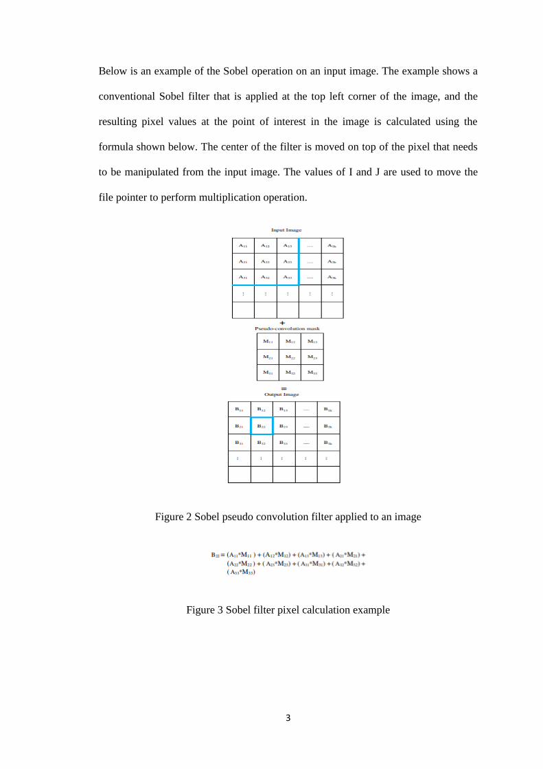
Below is an example of the Sobel operation on an input image. The example shows a
conventional Sobel filter that is applied at the top left corner of the image, and the
resulting pixel values at the point of interest in the image is calculated using the
formula shown below. The center of the filter is moved on top of the pixel that needs
to be manipulated from the input image. The values of I and J are used to move the
file pointer to perform multiplication operation.
Figure 2 Sobel pseudo convolution filter applied to an image
Figure 3 Sobel filter pixel calculation example

4
The gradient magnitude calculation formula is given below:
Figure 4 Gradient magnitude calculation
1.1.1.1 Pseudo Code for Sobel Edge Detection
a. Input the Sample image
b. Apply the convolution filters in both Gx and Gy directions.
c. Apply Sobel edge detection and the gradient on the input image
d. On the input image, apply convolution filters in Gx and Gy directions
separately.
e. Combine the magnitudes of the gradient calculated in both the directions to get
the absolute magnitude of the gradient.
f. The resulting magnitude of the gradient is the image with the edges in it.

5
CHAPTER 2
System-on-Chip Design Stages
2.1 Design
A system on chip includes both hardware functioning units like the microprocessor
which can be programmed using high level code like C/C++ and communication
systems like connect, control, direct and interface between the functional modules.
Basic idea behind SoC design is the development of both the hardware and software
modules at the same time. While designing the system, the optimizations and
constraints are also taken into account. The other key feature involved in the SoC
Design is the verification process.
After the architecture of the SoC is defined, the hardware elements required are
created at an abstract level using Hardware Description Language to define the
behaviour of the system or using C++ and synthesize the code into RTL using HLS
tools. These elements created are connected using HDL to create the entire SoC
design.
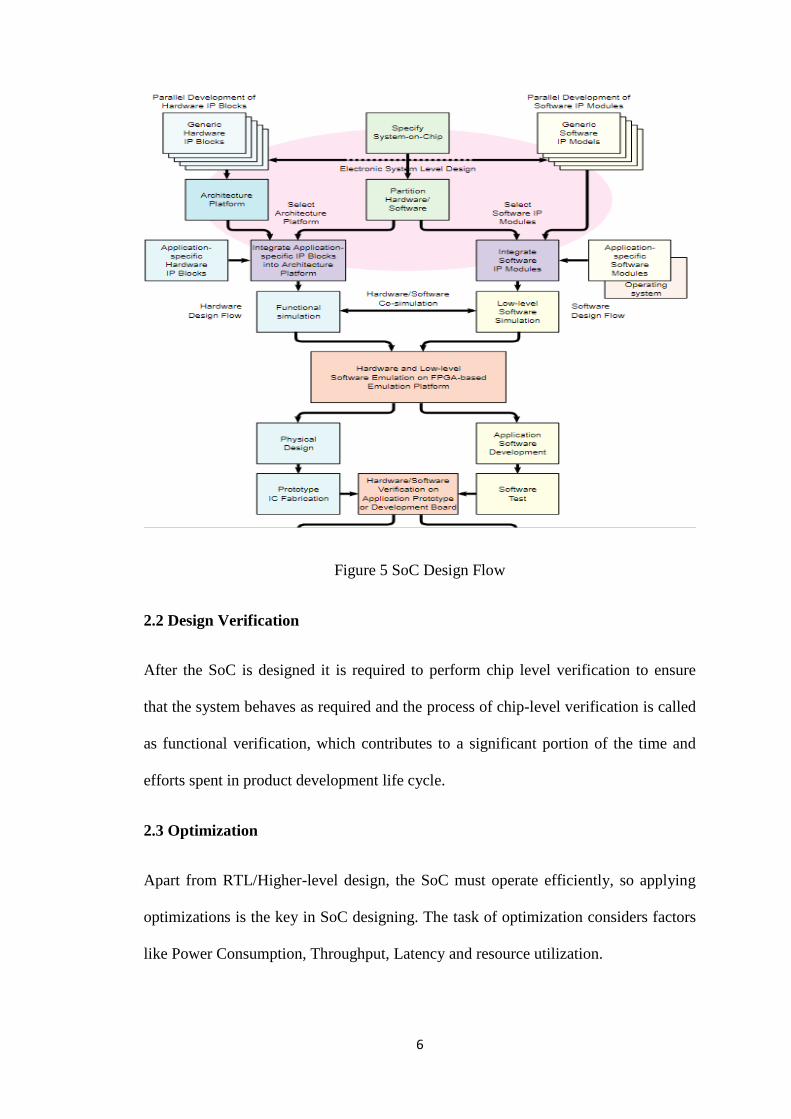
6
Figure 5 SoC Design Flow
2.2 Design Verification
After the SoC is designed it is required to perform chip level verification to ensure
that the system behaves as required and the process of chip-level verification is called
as functional verification, which contributes to a significant portion of the time and
efforts spent in product development life cycle.
2.3 Optimization
Apart from RTL/Higher-level design, the SoC must operate efficiently, so applying
optimizations is the key in SoC designing. The task of optimization considers factors
like Power Consumption, Throughput, Latency and resource utilization.

7
2.4 Fabrication
The optimization factors mentioned earlier is the basis for the place/route tool to
transform the designer’s intent into the SoC design. While transfomation is taking
place, the analysis of the design takes place using various methods of timing analysis,
simulations, and Logic analysers to confirm that the constraints related to timing,
signal integrity, etc. specified by the designer are met. Once the physical design
specifications are met, the files that describe each and every layer of the chip are sent
to the foundry’s mask shop for the etching process. These are then sent to the wafer
fabrication plant where the SoC dice is created, packaged and tested. SoCs are
customised using different types of technologies and some of the common ones are
Full Custom ASIC, Standard Cell ASIC and FPGAs.

8
CHAPTER 3
Hardware Acceleration Using HLS
3.1 High-Level Synthesis
High Level Synthesis (HLS) is a robotized configuration process in which the desired
algorithmic behaviour is interpreted and the digital hardware is created which
implements that behaviour. The main advantage is that use of HLS increases the level
of abstraction, while developing an FPGA application which saves time. Apart from
this, HLS also gives better control over optimizing the design architecture by
efficiently building and verifying the hardware.
The logic synthesis usually happens at RTL level, but in case of HLS we only define
the algorithm the system has to implement and the interconnect protocol. The HLS
tool handles the rest of the micro architecture design by transforming any untimed or
partially timed code into a fully synthesisable RTL code which gives a detailed cycle-
by-cycle implementation on the hardware.
Hardware Acceleration is the technique of utilizing computer hardware to perform
certain functions more efficiently than software-based implementation. Hardware
acceleration is peformed using Vivado HLS tool and its libraries such as:
HLS_OpenCV which enables us to leverage the OpenCV framework
HLS_Video library allows us to utilize the necessary image processing
functions.

9
3.1.1 Phases of HLS
The high level synthesis used to describe the design of the IP is untimed unlike the
Verilog/VHDL designs. Thus, when the HLS tool translates high level code into
Verilog/VHDL code, it goes through a number of stages before creating the RTL.
a. Scheduling – This stage determines and schedules execution of instructions
that are to be implemented.
b. Binding – This stage is for assigning the resources available on the device
once the scheduling phase is completed.
c. Control Logic Extraction – The control logic extraction phase is used to
extract the control signals and create control structures like creating state
machines to exert control over the behaviour of the model
Figure 6 HLS Scheduling and HLS Binding

10
Figure 7 HLS Control Logic Extraction Phase
While Performing the C synthesis, the HLS tool trades off between the performance
and logic resources availability which results in the performance of the IP core
implemented.

11
CHAPTER 4
Zybo Z7-20: Zynq-7000 ARM/FPGA SoC Development Board
4.1 Features of Zybo Z7-20
In this project, the Edge detection Algorithm is implemented on the Zybo Z7-20
board. The Zybo Z7 has a rich arrangement of media and network peripherals that can
be used to implement embedded vision algorithms like Edge detection, Object
tracking, etc. The Zybo Z7 is based on the Xilinx APSoC architecture which includes
a dual-core ARM Cortex-A9 processor with Xilinx 7-series FPGAs.
Figure 8 Zybo Z7-20
One of the features of the Zybo board used in this project is the HDMI input and
Output which enables attachment of a HDMI camera. The other key features of the
Zybo board include the following:
Figure 9 Key Features

12
4.2 Xilinx APSoC Architecture
The APSoC is a special kind of FPGA in which the ARM based processors as well as
the reconfigurable hardware on a chip is included. The block diagram of APSoC
architecture is given below. The architecture shows the PS sections marked in green
and PL section marked in yellow.
Figure 10 Block Diagram of Xilinx APSoC architecture

13
The APSoC features include the following
a. Processor Side: Dual core ARM Cortex – A9 MPCore processing system with
integrated memory controllers and peripherals. The ARM processor is
completely independent from the programmable logic
b. Programmable Logic: The firmly incorporated programmable rationale is used
to extend the processing system. It also provides high performance ARM AXI
interfaces. The PL side provides scalable density and performance.
c. Flexible Array of Input/Output: The APSoC provides wide scope of external
multi-standard I/O interfaces. It also provides HDMI IN and OUT that are
used in this project for real-time video streaming. The APSoC also has an elite
incorporated serial transceivers as well as Analog-to-Digital inputs.

14
CHAPTER 5
Image Processing Platform on Zybo Z7-20
The image processing platform is set-up on a Zybo-Z7 20 all programmable SOC that
enables HDMI input to output which is used as a base for HLS-based edge detection.
In addition to the Zybo the following is used in this project:
1. HDMI camera (Apeman 1080P action camera)
2. Cables for the HDMI input and output ports
3. HDMI monitor
The image streaming application is created using the following:
1. Vivado 2017.4
2. Xilinx SDK 2017.4
3. Digilent Vivado library (Download and Extract)
5.1 Components in the Block Diagram
In the Vivado block diagram we add the following IPs:
Zynq Processing System: The processing system is used to configure and
provide control signals for the whole image processing system. The DDR
of the processor is used as a DRAM buffer. The following configurations
are explicitly ensured:
a. PL clock 0 = 200 MHz
b. PL clock 1 = 100 MHz

15
c. HP 0 Slave enabled – The slave is used to transfer images to and from
the PS DDR
d. GP 0 Master enabled – This feature is used to configure and control
the flow of data in the whole image processing chain
Figure 11 Zynq Processing System

16
DVI2RGB:
a. This IP converts the HDMI image/video stream into a 24-bit RGB
format with the appropriate Hsync and Vsync.
b. The resolution is set 1280x720
Figure 12 DVI2RGB

17
AXI GPIO:
a. This IP provides universally useful input/output interface to AXI4-lite
interface.
b. The AXI GPIO is configured as a single output channel and the
reconfigurable width of the channel is set to 1.
c. We ensure that the AXI GPIO has a single output to ensure hot plug
detect from the HDMI source. Failure to assert this means that no
image/video is received from the camera module
Figure 13 AXI GPIO

18
Video Timing Controller:
a. The video timing controller IP is generally used with the input video
to AXI4-stream IP core that helps in detecting the format and timing of
the incoming video signal or with the AXI4-stream IP to video out to
create outgoing video timing for downstream sinks.
b. Here we configure the core to act as detector, which is used to detect
the mode of the incoming HDMI camera module.
Figure 14 Video Timing Controller (Detector)
19
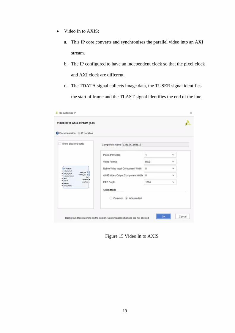
Video In to AXIS:
a. This IP core converts and synchronises the parallel video into an AXI
stream.
b. The IP configured to have an independent clock so that the pixel clock
and AXI clock are different.
c. The TDATA signal collects image data, the TUSER signal identifies
the start of frame and the TLAST signal identifies the end of the line.
Figure 15 Video In to AXIS

20
AXIS Subset Converter:
a. This IP provides re-map functionality using which the
TDATA/TUSER can be re-mapped into the correct RGB format.
b. The TDATA width is configured to 3 bytes
c. Here we use two of this IP core which is before and after the VDMA
Figure 16 AXI-4 Stream Subset Converter

21
Video Direct Memory:
a. This IP core is used to store the AXI stream video into AXI memory
mapped form for storage in the PS DDR memory.
b. For the output, the read channel accesses the PS DDR to convert the
AXI memory mapped into AXI stream.
c. Because we need to store as well as stream the video for the output, we
ensure that both the read and write channels are enabled.
Figure 17 VDMA
22
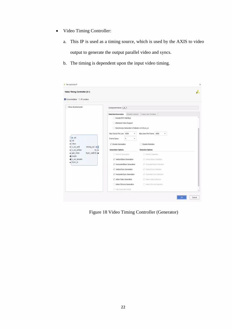
Video Timing Controller:
a. This IP is used as a timing source, which is used by the AXIS to video
output to generate the output parallel video and syncs.
b. The timing is dependent upon the input video timing.
Figure 18 Video Timing Controller (Generator)

23
RGB2DVI:
a. This IP converts the vertical/horizontal syncs along with the output
parallel video into HDMI format, for display purposes using an HDMI
monitor.
Figure 19 RGB2DVI
Dynamic Clock Generator:
a. To configure the output clocks dynamically, the dynamic clock
generator is used.
b. This enables the pixel clock frequency to be changed over using AXI-
lite depending on the video format received.

24
CHAPTER 6
Sobel Filter IP Creation Using Vivado HLS
The Sobel edge detection IP is created using HLS functions, which helps us in
skipping out the traditional RTL way of implementation on the FPGA. In case of the
RTL approach, it is required to create line buffers for the convolution filters and then
implement the magnitude calculation whereas, in case of High Level Synthesis, the
HLS tool will take care of the lower level RTL implementation.
6.1 Implementation
The IP is implemented using Vivado HLS and its HLS_OpenCV and HLS_Video
libraries that increase the levels of abstraction. To leverage the OpenCV framework
which is popular for implementing image processing algorithms, the HLS_OpenCV
library is used.
Some of the functions of the HLS_Video library used in this project are:
a. HLS::CvtColor – “This converts the color scheme between color and gray
scale depending upon the configuration”
b. HLS::Gaussian – “The Gaussian blurring is applied to the input image for
noise removal and image smoothening.”
c. HLS::Sobel – “Depending on the configuration, this function can be used to
apply Sobel convolution in either horizontal or vertical directions. Here two
implementations of this IP core are used as we need the convolution in both
the directions for the magnitude calculation.”

25
d. HLS::AddWeighted – “This IP core allows us to calculate the resulting
magnitude calculation using the results of the Sobel operator in both the
directions.”
6.2 Interfacing
The AXI stream is used to move image data within the programmable logic enabling
the creation of a high performance image processing path required for easy addition
and creation of elements.
As the Sobel IP has to be able to accept AXI stream input and generate its output in
the same format, below functions from Vivado HLS library is used.
a. HLS::AXIvideo2Mat – “Converts an AXI stream image/video into HLS::Mat
format on which further image processing algorithms can be implemented.”
b. HLS::Mat2AXIvideo – “Converts the image from HLS::Mat format to AXI
stream format, which is used for displaying the result of edge detection.”
6.3 C Synthesis and Optimizations
For optimization, the Dataflow #pragma is used in the C code to achieve the highest
possible frame rate.
The Sobel operation in both the directions is performed parallel, so that the use of
dataflow pragma ensures coarse grain pipelining.

26
Figure 20 Dataflow Pipelining
To apply the pipelining optimization the result of the Gaussian blurring is split into
two parallel paths and then recombined using the HLS::AddWeighted function to
calculate the magnitude of the gradient. The splitting is done using the
HLS::Duplicate that duplicates the Gaussian blurred image in two separate output
images that can be processed in parallel.
After the High level code is ready, the C simulation and synthesis is performed which
produces the output image in which the edges are extracted from the input image.
The high level code for implementing the Sobel IP core along with the video
streaming code to display the result of edge detection is given in the appendix. It
includes the header file, test-bench and the Sobel filter function code.

27
CHAPTER 7
SOFTWARE APPLICATION
After the block diagram is ready, the bitstream generated is built and exported to
Xilinx SDK to create the video streaming application. The software application
written in C will do the following:
a. The GPIO which is connected to the HDMI IN hot plug detect is asserted. The
HDMI source generates the video after a wait time of about 5 seconds, when
this signal is asserted
b. The Video Timing Controller acting as the detector is configured to report the
incoming video mode.
c. The Video Timing Controller acting as the generator is configured to generate
the timing in accordance with the video mode detected.
d. The dynamic clock is configured.
e. The VDMA is configured to have read/write access from the PS DDR.
The software application required for video streaming is given in the appendix.

28
CHAPTER 8
RESULTS AND ANALYSIS
8.1 C and Co Simulation Results
The input image provided for C and Co Simulation is:
Figure 21 Input Image for C and Co Simulation
The resulting output image with the edges extracted is:
Figure 22 Result of C and Co Simulation

29
8.2 Resource Utilization
Before exporting to HLS IP to the Vivado IP repository, the resources utilized by the
IP are analysed to ensure that the IP can be implemented on the Zybo board.
The analysis also confirms that the two Sobel operators used in the IP design using
dataflow pragma are working in parallel.
Figure 23 Parallel Sobel Operations
The summary of the performance estimates of the HLS IP are as below:
Figure 24 Performance Estimates

30
The summary of the resource utilisation of the HLS IP is as follows:
Figure 25 Resource Utilization
From the estimates above, it is clear that the resource utilized to implement the HLS
IP is less than the total available resources on the Zybo Z7 20 board.
After exporting the IP, a zip file containing all the necessary information required to
add the newly created Sobel IP is generated.
This file is added to the user IP repository in Vivado 2017.4 to integrate the HLS IP
with the image processing platform and the edge detection in real time is
implemented.

31
CHAPTER 9
CONCLUSION
Edge detection is almost everywhere when it comes to computer vision solutions like
ADAS, consumer products, retail etc. Designing these solutions using pure Hardware
Description Language is not easy because of the constant algorithm upgrades, which
means the RTL team involved in creation and verification flow will have to start over
which is highly undesirable and leads to delays in the production schedule. The only
solution to this is to adopt High-Level Synthesis design flow because high level
coding is easier to maintain, modify and re-use.
In this project an example of how to implement edge detection is successfully
demonstrated by integrating an Apeman HD camera with the very powerful Zynq
device which is used extensively in the field of image processing.
Although the objective of the project is accomplished, there is a lot of scope for
improvement because the Zynq can be used to implement more complex image
processing applications like Lane detection, Object tracking, etc., which I intend to
implement in the future.

32
Bibliography
[1] Adam Taylor (2018, May 11). “Creating a Zynq or FPGA-Based, Image
Processing Platform”.
https://www.hackster.io/adam-taylor/creating-a-zynq-or-fpga-based-image-
processing-platform-e79394
[2] “Digital Image Processing”. Retrieved from Wikipedia
https://en.wikipedia.org/wiki/Digital_image_processing
[3] Processing System 7 v5.5 LogiCORE IP Product Guide
https://www.xilinx.com/support/documentation/ip_documentation/processing_system
7/v5_5/pg082-processing-system7.pdf
[4] AXI Video Direct Memory Access v6.3 LogiCORE IP Product Guide
https://www.xilinx.com/support/documentation/ip_documentation/axi_vdma/v6_3/pg
020_axi_vdma.pdf
[5] Video Timing Controller v6.1 LogiCORE IP Product Guide.
https://www.xilinx.com/support/documentation/ip_documentation/v_tc/v6_1/pg016_v
_tc.pdf
[6] Jeff Johnson (2014, August 6). “Using the AXI DMA in Vivado”
http://www.fpgadeveloper.com/2014/08/using-the-axi-dma-in-vivado.html
[7] Zynq-7000, Technical Reference Manual
https://www.xilinx.com/support/documentation/user_guides/ug585-Zynq-7000-
TRM.pdf
[8] XAPP1167, Accelerating OpenCV Applications with Zynq-7000 All
Programmable SoC using Vivado HLS Video Libraries
https://www.xilinx.com/support/documentation/application_notes/xapp1167.pdf

33
[9] XAPP890, Zynq All Programmable SoC Sobel Filter Implementation Using the
Vivado HLS Tool
https://www.xilinx.com/support/documentation/application_notes/xapp890-zynq-
sobel-vivado-hls.pdf
[10] Vivado Design Suit User Guide, High Level Synthesis
https://www.xilinx.com/support/documentation/sw_manuals/xilinx2014_1/ug902-
vivado-high-level-synthesis.pdf
[11] Samta Gupta, Susmita Ghosh Mazumdar (2013, February 2). “Sobel Edge
Detection Algorithm”
https://pdfs.semanticscholar.org/6bca/fdf33445585966ee6fb3371dd1ce15241a62.pdf

34
APPENDIX
Camera used for HDMI input to the Zybo:
Figure 26 Apeman Action Camera
Some of the features of the camera include:
a. Resolution: 1280 x 720
b. 14MP 1080P full HD
c. 2-inch LCD display

35
High-Level Synthesis source codes:
Filename: cvt_colour.cpp
/************************************************************************** * Engineer: Pavan Kumar Murthy * Create Date: 03/14/2019 * File Name: cvt_colour.cpp * Description: This file is used apply sobel operator on the input image **************************************************************************/ #include "cvt_colour.h" void image_filter(STRM_AXI& STRM_IN, STRM_AXI& STRM_OUT) { #pragma HLS INTERFACE axis port=STRM_IN #pragma HLS INTERFACE axis port=STRM_OUT EDGE_RGB edge_0(EDGE_HHT, EDGE_WTH); EDGE_GRY edge_1(EDGE_HHT, EDGE_WTH); EDGE_GRY edge_2(EDGE_HHT, EDGE_WTH); EDGE_GRY edge_2a(EDGE_HHT, EDGE_WTH); EDGE_GRY edge_2b(EDGE_HHT, EDGE_WTH); EDGE_GRY edge_3(EDGE_HHT, EDGE_WTH); EDGE_GRY edge_4(EDGE_HHT, EDGE_WTH); EDGE_GRY edge_5(EDGE_HHT, EDGE_WTH); EDGE_RGB edge_6(EDGE_HHT, EDGE_WTH); ; #pragma HLS dataflow hls::AXIvideo2Mat(STRM_IN, edge_0); hls::CvtColor<HLS_BGR2GRAY>(edge_0, edge_1); hls::GaussianBlur<3,3>(edge_1,edge_2); hls::Duplicate(edge_2,edge_2a,edge_2b); hls::Sobel<1,0,3>(edge_2a, edge_3); hls::Sobel<0,1,3>(edge_2b, edge_4); hls::AddWeighted(edge_4,0.5,edge_3,0.5,0.0,edge_5); hls::CvtColor<HLS_GRAY2RGB>(edge_5, edge_6); hls::Mat2AXIvideo(edge_6, STRM_OUT); }

36
Filename: cvt_colour.h
/************************************************************************** * Engineer: Pavan Kumar Murthy * Create Date: 03/14/2019 * File Name: cvt_colour.h * Description: This file is used as header for cvt_colour.cpp **************************************************************************/ #include "hls_video.h" #include <ap_fixed.h> #define EDGE_WTH 1280 #define EDGE_HHT 720 typedef hls::stream<ap_axiu<24,1,1,1> > STRM_AXI; typedef hls::Mat<EDGE_HHT, EDGE_WTH, HLS_8UC3> EDGE_RGB; typedef hls::Mat<EDGE_HHT, EDGE_WTH, HLS_8UC1> EDGE_GRY; void image_filter(STRM_AXI& STRM_IN, STRM_AXI& STRM_OUT);

37
Filename: cvt_colour_tb.cpp
/************************************************************************** * Engineer: Pavan Kumar Murthy * Create Date: 03/14/2019 * File Name: cvt_colour.h * Description: This file is used as a testbench for cvt_colour.cpp **************************************************************************/ #include <hls_opencv.h> #include "cvt_colour.h" #include <iostream> using namespace std; int main (int argc, char** argv) { IplImage* srceImg; IplImage* dstnImg; STRM_AXI srceAxiStrm, dstnAxiStrm; srceImg = cvLoadImage("sample.bmp"); dstnImg = cvCreateImage(cvGetSize(srceImg), srceImg->depth, srceImg->nChannels); IplImage2AXIvideo(srceImg, srceAxiStrm); image_filter(srceAxiStrm, dstnAxiStrm); AXIvideo2IplImage(dstnAxiStrm, dstnImg); cvSaveImage("edge.bmp", dstnImg); cvReleaseImage(&srceImg); cvReleaseImage(&dstnImg); }

38
SDK software application:
Filename: helloworld.c
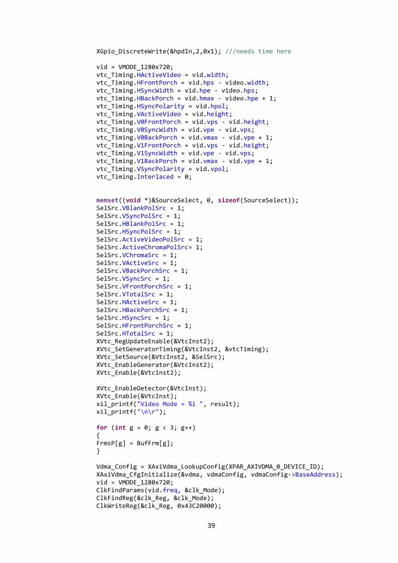
/************************************************************************ * Engineer: Pavan Kumar Murthy * Create Date: 03/21/2019 * File name: helloworld.c * Description: This file is used to stream real-time edge detection vide ************************************************************************/ #include <stdio.h> #include "platform.h" #include "xil_printf.h" #include "xparameters.h" #include "xgpio.h" #include "xvtc.h" #include "xaxivdma.h" #include "xaxivdma_i.h" #include "vga_modes.h" #include "dynclk.h" #define DEMO_IMG_FRAME (720*1280) #define DEMO_IMG_STRIDE (1280*3) #define DISPLAY_IMG_FRAMES 3 XVtc VtcInst0,VtcInst1; XVtc_Config *vtc_config0,*vtc_config1 ; XGpio hpdIn; XAxiVdma vdma; XAxiVdma_DmaSetup vdma_DMA; XAxiVdma_Config *vdma_Config; ClkConfig clk_Reg; ClkMode clk_Mode; u32 BufFrm[DISPLAY_IMG_FRAMES][DEMO_IMG_FRAME]; u32 *FrmsP[DISPLAY_IMG_FRAMES]; VideoMode vid; int main() { init_platform(); disable_caches(); XVtc_Timing vtc_Timing; XVtc_SourceSelect SelSrc; int op_status; u16 res; vtc_config = XVtc_LookupConfig(XPAR_VTC_0_DEVICE_ID); XVtc_CfgInitialize(&VtcInst, vtc_config, vtc_config->BaseAddress); vtc_config2 = XVtc_LookupConfig(XPAR_VTC_1_DEVICE_ID); XVtc_CfgInitialize(&VtcInst2, vtc_config2, vtc_config2>BaseAddress); //asserting the Hot Plug Detect XGpio_Initialize(&hpdIn, XPAR_AXI_GPIO_0_DEVICE_ID); XGpio_DiscreteWrite(&hpdIn,1,0x1); sleep(20);
39
XGpio_DiscreteWrite(&hpdIn,2,0x1); ///needs time here vid = VMODE_1280x720; vtc_Timing.HActiveVideo = vid.width; vtc_Timing.HFrontPorch = vid.hps - video.width; vtc_Timing.HSyncWidth = vid.hpe - video.hps; vtc_Timing.HBackPorch = vid.hmax - video.hpe + 1; vtc_Timing.HSyncPolarity = vid.hpol; vtc_Timing.VActiveVideo = vid.height; vtc_Timing.V0FrontPorch = vid.vps - vid.height; vtc_Timing.V0SyncWidth = vid.vpe - vid.vps; vtc_Timing.V0BackPorch = vid.vmax - vid.vpe + 1; vtc_Timing.V1FrontPorch = vid.vps - vid.height; vtc_Timing.V1SyncWidth = vid.vpe - vid.vps; vtc_Timing.V1BackPorch = vid.vmax - vid.vpe + 1; vtc_Timing.VSyncPolarity = vid.vpol; vtc_Timing.Interlaced = 0; memset((void *)&SourceSelect, 0, sizeof(SourceSelect)); SelSrc.VBlankPolSrc = 1; SelSrc.VSyncPolSrc = 1; SelSrc.HBlankPolSrc = 1; SelSrc.HSyncPolSrc = 1; SelSrc.ActiveVideoPolSrc = 1; SelSrc.ActiveChromaPolSrc= 1; SelSrc.VChromaSrc = 1; SelSrc.VActiveSrc = 1; SelSrc.VBackPorchSrc = 1; SelSrc.VSyncSrc = 1; SelSrc.VFrontPorchSrc = 1; SelSrc.VTotalSrc = 1; SelSrc.HActiveSrc = 1; SelSrc.HBackPorchSrc = 1; SelSrc.HSyncSrc = 1; SelSrc.HFrontPorchSrc = 1; SelSrc.HTotalSrc = 1; XVtc_RegUpdateEnable(&VtcInst2); XVtc_SetGeneratorTiming(&VtcInst2, &vtcTiming); XVtc_SetSource(&VtcInst2, &SelSrc); XVtc_EnableGenerator(&VtcInst2); XVtc_Enable(&VtcInst2); XVtc_EnableDetector(&VtcInst); XVtc_Enable(&VtcInst); xil_printf("Video Mode = %i ", result); xil_printf("\n\r"); for (int g = 0; g < 3; g++) { FrmsP[g] = BufFrm[g]; } Vdma_Config = XAxiVdma_LookupConfig(XPAR_AXIVDMA_0_DEVICE_ID); XAxiVdma_CfgInitialize(&vdma, vdmaConfig, vdmaConfig->BaseAddress); vid = VMODE_1280x720; ClkFindParams(vid.freq, &clk_Mode); ClkFindReg(&clk_Reg, &clk_Mode); ClkWriteReg(&clk_Reg, 0x43C20000);

40
ClkStop(0x43C20000); ClkStart(0x43C20000); vdma_DMA.FrameDelay = 0; vdma_DMA.EnableCircularBuf = 1; vdma_DMA.EnableSync = 0; vdma_DMA.PointNum = 0; vdma_DMA.EnableFrameCounter = 0; vdma_DMA.VertSizeInput = vid.height; vdma_DMA.HoriSizeInput = (vid.width)*3; vdma_DMA.FixedFrameStoreAddr = 0; vdma_DMA.FrameStoreStartAddr[0] = (u32) FrmsP[0]; vdma_DMA.Stride = (vid.width)*3; XAxiVdma_DmaConfig(&vdma, XAXIVDMA_WRITE, &(vdma_DMA)); op_status = XAxiVdma_DmaSetBufferAddr(&vdma, XAXIVDMA_WRITE,vdma_DMA.FrameStoreStartAddr); op_status = XAxiVdma_DmaStart(&vdma, XAXIVDMA_WRITE); op_status = XAxiVdma_StartParking(&vdma, 0, XAXIVDMA_WRITE); XAxiVdma_DmaConfig(&vdma, XAXIVDMA_READ, &(vdma_DMA)); XAxiVdma_DmaSetBufferAddr(&vdma, XAXIVDMA_READ,vdma_DMA.FrameStoreStartAddr); XAxiVdma_DmaStart(&vdma, XAXIVDMA_READ); XAxiVdma_StartParking(&vdma, 0, XAXIVDMA_READ); while(1) { } return 0; }

41
Block Diagram of the Image Processing Platform:
Part 1:
Figure 27 Image Processing Platform (Part 1)

42
Part 2:
Figure 28 Image Processing Platform (Part 2)

43
Part 3:
Figure 29 Image Processing Platform (Part 3)

44
Complete Block Diagram with the HLS IP Integrated:
Part 1:
Figure 30 HLS IP Integrated within the Image Processing Platform (Part 1)

45
Part 2:
Figure 31 HLS IP Integrated within the Image Processing Platform (Part 2)

46
Part 3:
Figure 32 HLS IP Integrated within the Image Processing Platform (Part 3)

47
Part 4:
Figure 33 HLS IP Integrated within the Image Processing Platform (Part 4)

48
Part 5:
Figure 34 HLS IP Integrated within the Image Processing Platform (Part 5)