cc2564c dual-mode bluetooth controller · external calibration required ... b24 b23 b22 b21 b20 a29...
TRANSCRIPT

Product
Folder
Sample &Buy
Technical
Documents
Tools &
Software
Support &Community
An IMPORTANT NOTICE at the end of this data sheet addresses availability, warranty, changes, use in safety-critical applications,intellectual property matters and other important disclaimers. PRODUCTION DATA.
CC2564CSWRS199A –APRIL 2016–REVISED NOVEMBER 2016
CC2564C Dual-Mode Bluetooth® Controller
1 Device Overview
1
1.1 Features1
• TI's Single-Chip Bluetooth® Solution WithBluetooth Basic Rate (BR), Enhanced Data Rate(EDR), and Low Energy (LE) Support
• Bluetooth 4.2 Component Qualified (DeclarationID: D032801); Compliant up to the HCI Layer
• Highly Optimized for Size-Constrained and Low-Cost Designs:– Single-Ended 50-Ω RF Interface– Package Footprint: 76 Terminals, 0.6-mm Pitch,
8-mm × 8-mm (VQFNP-MR)• BR and EDR Features Include:
– Up to Seven Active Devices– Scatternet: Up to Three Piconets
Simultaneously, One as Master and Two asSlaves
– Up to Two Synchronous Connection Oriented(SCO) Links on the Same Piconet
– Support for All Voice Air-Coding—ContinuouslyVariable Slope Delta (CVSD), A-Law, µ-Law,Modified Subband Coding (mSBC), andTransparent (Uncoded)
– Provide an Assisted Mode for HFP 1.6Wideband Speech (WBS) Profile or A2DPProfile to Reduce Host Processing and Power
– Support of Multiple Bluetooth Profiles WithEnhanced QoS
• Low Energy Features Include:– Multiple Sniff Instances Tightly Coupled to
Achieve Minimum Power Consumption– Independent Buffering for Low Energy Allows
Large Numbers of Multiple Connections WithoutAffecting BR or EDR Performance
– Built-In Coexistence and Prioritization Handlingfor BR, EDR, and Low Energy
– Capabilities of Link Layer TopologyScatternet—Can Act Concurrently as Peripheraland Central
– Network Support for up to 10 Devices– Time Line Optimization Algorithms to Achieve
Maximum Channel Utliization• Best-in-Class Bluetooth (RF) Performance (TX
Power, RX Sensitivity, Blocking)– Class 1 TX Power up to +12 dBm– Internal Temperature Detection and
Compensation to Ensure Minimal Variation inRF Performance Over Temperature, NoExternal Calibration Required
– Improved Adaptive Frequency Hopping (AFH)Algorithm With Minimum Adaptation Time
– Longer Range, Including Twice the Range ofOther Low-Energy-Only Solutions
• Advanced Power Management for ExtendedBattery Life and Ease of Design– On-Chip Power Management, Including Direct
Connection to Battery– Low Power Consumption for Active, Standby,
and Scan Bluetooth Modes– Shutdown and Sleep Modes to Minimize Power
Consumption• Physical Interfaces:
– UART Interface With Support for MaximumBluetooth Data Rates• UART Transport Layer (H4) With Maximum
Rate of 4 Mbps• Three-Wire UART Transport Layer (H5) With
Maximum Rate of 4 Mbps– Fully Programmable Digital Pulse-Code
Modulation (PCM)–Inter-IC Sound (I2S) CodecInterface
• Flexibility for Easy Stack Integration and ValidationInto MCUs and MPUs
• CC256x Bluetooth Hardware Evaluation Tool:PC-Based Application to Evaluate RF Performanceof the Device and Configure Service Pack
1.2 Applications• Wireless Audio Solutions• mPOS• Medical Devices• Set-Top Boxes (STBs)
• Wearable Devices• Sensor Hub, Sensor Gateway
– Home and Factory Automation

PCM-I2S
UART
CC2564C
I/Ointerface
Coprocessor(See Note)
BR/EDRmain processor
Modemarbitrator
DRP
Powermanagement
Clockmanagement
2.4-GHzband-pass filter
HCI
Slowclock
Fastclock
Power Shutdown
Copyright © 2016, Texas Instruments Incorporated
2
CC2564CSWRS199A –APRIL 2016–REVISED NOVEMBER 2016 www.ti.com
Submit Documentation FeedbackProduct Folder Links: CC2564C
Device Overview Copyright © 2016, Texas Instruments Incorporated
(1) For more information on these devices, see Section 9.
1.3 DescriptionThe TI CC2564C device is a complete Bluetooth® BR, EDR, and low energy HCI solution that reducesdesign effort and enables fast time to market. Based on TI’s seventh-generation Bluetooth core, theCC2564C device provides a product-proven solution that is Bluetooth 4.2 compliant. When coupled with amicrocontroller unit (MCU), this HCI device offers best-in-class RF performance with about twice the rangeof other Bluetooth low-energy solutions. Furthermore, TI’s power-management hardware and softwarealgorithms provide significant power savings in all commonly used Bluetooth BR, EDR, and low energymodes of operation.
The TI dual-mode Bluetooth stack software is certified and provided royalty free for MCUs and MPUs. TheiPod® (MFi) protocol is supported by add-on software packages. For more information, see TI Dual-ModeBluetooth Stack. Multiple profiles and sample applications are supported including the following:
Serial port profile (SPP)Advanced audio distribution profile (A2DP)Audio/video remote control profile (AVRCP)Hands-free profile (HFP)Human interface device (HID)Generic attribute profile (GATT)Several Bluetooth low energy profiles and services
Device Information (1)
PART NUMBER PACKAGE BODY SIZECC2564CRVM RVM (76) 8.00 mm × 8.00 mm × 0.60 mm
space1.4 Functional Block Diagram
Note: The following technologies and assisted modes cannot be used simultaneously with the coprocessor: Bluetooth lowenergy, assisted HFP 1.6 (WBS), and assisted A2DP. Only one technology or assisted mode can be used at a time.
Figure 1-1. Functional Block Diagram

3
CC2564Cwww.ti.com SWRS199A –APRIL 2016–REVISED NOVEMBER 2016
Submit Documentation FeedbackProduct Folder Links: CC2564C
Revision HistoryCopyright © 2016, Texas Instruments Incorporated
Table of Contents1 Device Overview ......................................... 1
1.1 Features .............................................. 11.2 Applications........................................... 11.3 Description............................................ 21.4 Functional Block Diagram ............................ 2
2 Revision History ......................................... 33 Device Comparison ..................................... 4
3.1 Related Products ..................................... 44 Terminal Configuration and Functions ............. 5
4.1 VQFN-MR Pin Diagram............................... 55 Specifications ............................................ 8
5.1 Absolute Maximum Ratings .......................... 85.2 ESD Ratings.......................................... 85.3 Power-On Hours...................................... 85.4 Recommended Operating Conditions ................ 95.5 Power Consumption Summary ....................... 95.6 Electrical Characteristics ............................ 115.7 Thermal Resistance Characteristics for VQFN-MR
(RVM) Package .................................... 115.8 Timing and Switching Characteristics ............... 12
6 Detailed Description ................................... 236.1 Overview ............................................ 23
6.2 Functional Block Diagram........................... 236.3 Clock Inputs ......................................... 236.4 Functional Blocks.................................... 276.5 Bluetooth® BR and EDR Features .................. 386.6 Bluetooth® low energy Description.................. 396.7 Bluetooth® Transport Layers ........................ 406.8 Changes from the CC2564B Device to the
CC2564C Device.................................... 407 Applications, Implementation, and Layout........ 41
7.1 Reference Design Schematics and BOM for Powerand Radio Connections ............................. 41
7.2 PCB Layout Guidelines ............................. 438 Device and Documentation Support ............... 47
8.1 Third-Party Products Disclaimer .................... 478.2 Tools and Software ................................. 478.3 Device Nomenclature ............................... 478.4 Documentation Support ............................. 488.5 Community Resources .............................. 488.6 Trademarks.......................................... 488.7 Electrostatic Discharge Caution..................... 488.8 Glossary ............................................. 48
9 Mechanical, Packaging, and OrderableInformation .............................................. 49
2 Revision HistoryNOTE: Page numbers for previous revisions may differ from page numbers in the current version.
Changes from April 8, 2016 to October 27, 2016 Page
• Updated document to PRODUCTION DATA ..................................................................................... 1

4
CC2564CSWRS199A –APRIL 2016–REVISED NOVEMBER 2016 www.ti.com
Submit Documentation FeedbackProduct Folder Links: CC2564C
Device Comparison Copyright © 2016, Texas Instruments Incorporated
(1) The assisted modes (HFP 1.6 and A2DP) are not supported simultaneously. Furthermore, the assisted modes are not supportedsimultaneously with Bluetooth low energy.
3 Device Comparison
Table 3-1 lists the features of the CC2564C device.
Table 3-1. CC2564C Device Features
DEVICE DESCRIPTIONTECHNOLOGY SUPPORTED ASSISTED MODES
SUPPORTED (1)
BR, EDR LOWENERGY
HFP 1.6(WBS) A2DP
CC2564C Bluetooth 4.2 + Bluetooth low energy √ √ √ √
3.1 Related ProductsWireless Connectivity The wireless connectivity portfolio offers a wide selection of low-power RF
solutions suitable for a broad range of application. The offerings range from fully customizedsolutions to turnkey offerings with precertified hardware and software (protocol).
Companion Products Review products that are frequently purchased or used with the CC2564C product.Reference Designs for CC2564 The TI Designs Reference Design Library is a robust reference design
library spanning analog, embedded processor, and connectivity. Created by TI experts tohelp you jump-start your system design, all TI Designs include schematic or block diagrams,BOMs and design files to speed your time to market. Search and download designs atti.com/tidesigns.

A30
A21
A31
A40
A1
A10
A11
A20
B19
B18
B10
B9
B1
B36
B28
B27
A2
A3
A4
A5
A6
A7
A8
A9
B2
B3
B4
B5
B6
B7
B8
B26
B25
B24
B23
B22
B21
B20
A29
A28
A27
A26
A25
A24
A23
A22
A32
A33
A34
A35
A36
A37
A38
A39
B29
B30
B31
B32
B33
B34
B35
B17
B16
B15
B14
B13
B12
B11
A19
A18
A17
A16
A15
A14
A13
A12
NC
NC
DIG_LDO_OUT
DIG_LDO_OUT
XTALM/FREFM
MLDO_OUT
nSHUTD
CL1.5_LDO_OUT
ADC_PPA_LDO_OUT
MLDO_OUT
NC
SRAM_LDO_OUT
MLDO_OUT
VSS_FREF
XTALP/FREFP
MLDO_IN
CL1.5_LDO_IN
MLDO_OUT
BT_RF
NC
NC
HCI_CTS
VSS
NC
HCI_RX
SLOW_CLK
VSS
NC
NC
VDD_IO
DIG_LDO_OUT
DIG_LDO_OUT
VDD_IO
TX_DBG
NC
VDD_IO
VDD_IO
NC
NC
NC
NC
NC
VD
D_IO
DC
O_LD
O_O
UT
VD
D_IO NC
NC
NC
DIG
_LD
O_O
UT
VS
S_D
CO
NC
NC
HC
I_R
TS
HC
I_T
X
VD
D_IO
AU
D_F
SY
NC
NC
VD
D_IO
DIG
_LD
O_O
UT
NC
NC
AU
D_C
LK
AU
D_O
UT
AU
D_IN
DIG
_LD
O_O
UT
SWRS121-002
NC
NC
NC
NC
NC
NC
NC
NC
NC
NC
NC
5
CC2564Cwww.ti.com SWRS199A –APRIL 2016–REVISED NOVEMBER 2016
Submit Documentation FeedbackProduct Folder Links: CC2564C
Terminal Configuration and FunctionsCopyright © 2016, Texas Instruments Incorporated
4 Terminal Configuration and Functions
4.1 VQFN-MR Pin DiagramFigure 4-1 shows the bottom view of the pin diagram (VQFN-MR package).
Figure 4-1. VQFN-MR Package Pin DiagramBottom View

6
CC2564CSWRS199A –APRIL 2016–REVISED NOVEMBER 2016 www.ti.com
Submit Documentation FeedbackProduct Folder Links: CC2564C
Terminal Configuration and Functions Copyright © 2016, Texas Instruments Incorporated
(1) I = input; O = output; I/O = bidirectional(2) I/O Type: Digital I/O cells. HY = input hysteresis, current = typical output current
4.1.1 Pin Attributes (VQFN-MR Package)Table 4-1 describes the pin attributes for the VQFN-MR package.
SPACER
Table 4-1. Pin Attributes (VQFN-MR Package)
NAME NO. PULL ATRESET
DEF.DIR. (1)
I/OType (2) DESCRIPTION
I/O Signals
AUD_CLK B32 PD I/O HY, 4mA PCM clock Fail-safe
AUD_FSYNC A35 PD I/O 4 mA PCM frame-sync signal Fail-safeAUD_IN B34 PD I 4 mA PCM data input Fail-safeAUD_OUT B33 PD O 4 mA PCM data output Fail-safe
HCI_CTS A29 PU I 8 mAHCI UART clear-to-sendThe device is allowed to send datawhen HCI_CTS is low.
HCI_RX A26 PU I 8 mAHCI universal asynchronousreceiver/transmitter (UART) datareceive
HCI_RTS A32 PU O 8 mAHCI UART request-to-sendThe host is allowed to send data whenHCI_RTS is low.
HCI_TX A33 PU O 8 mA HCI UART data transmit
TX_DBG B24 PU O 2 mATI internal debug messages. TIrecommends leaving an internal testpoint.
Clock SignalsSLOW_CLK A25 I 32.768-kHz clock in Fail-safe
XTALP/FREFP B4 I Fast clock in analog (sine wave)Output terminal of fast-clock crystal Fail-safe
XTALM/FREFM A4 I Fast clock in digital (square wave)Input terminal of fast-clock crystal Fail-safe
Analog SignalsBT_RF B8 I/O Bluetooth RF I/OnSHUTD A6 PD I Shutdown input (active low)Power and Ground SignalsADC_PPA_LDO_OUT A8 O ADC/PPA LDO output
CL1.5_LDO_IN B6 I Power amplifier (PA) LDO inputConnect directly to battery
CL1.5_LDO_OUT A7 O PA LDO outputDCO_LDO_OUT A12 O DCO LDO output
DIG_LDO_OUT
A2, A3,B15,B26,B27,
B35, B36
O
Digital LDO outputQFN pin B26 or B27 must be shortedto other DIG_LDO_OUT pins on thePCB.
MLDO_IN B5 I Main LDO inputConnect directly to battery
MLDO_OUT A5, A9,B2, B7 I/O Main LDO output (1.8-V nominal)
SRAM_LDO_OUT B1 O SRAM LDO output

7
CC2564Cwww.ti.com SWRS199A –APRIL 2016–REVISED NOVEMBER 2016
Submit Documentation FeedbackProduct Folder Links: CC2564C
Terminal Configuration and FunctionsCopyright © 2016, Texas Instruments Incorporated
Table 4-1. Pin Attributes (VQFN-MR Package) (continued)
NAME NO. PULL ATRESET
DEF.DIR. (1)
I/OType (2) DESCRIPTION
VDD_IO
A17,A34,A38,B18,B19,B21,
B22, B25
I I/O power supply (1.8-V nominal)
VSS A24, A28 I GroundVSS_DCO B11 I DCO groundVSS_FREF B3 I Fast clock ground
4.1.2 Connections for Unused Signals (VQFN-MR Package)Section 4.1.2 lists the connections for unused signals for the VQFN-MR package.
SPACERFUNCTION PIN NUMBER DESCRIPTION
NC A1 Not connectedNC A10 Not connectedNC A11 Not connectedNC A14 Not connectedNC A18 Not connectedNC A19 Not connectedNC A20 Not connectedNC A21 Not connectedNC A22 Not connectedNC A23 Not connectedNC A27 Not connectedNC A30 Not connectedNC A31 Not connectedNC A40 Not connectedNC B9 Not connectedNC B10 Not connectedNC B16 Not connectedNC B17 Not connectedNC B20 Not connectedNC B23 Not connectedNC A13 TI internal useNC A15 TI internal useNC A16 TI internal useNC A36 TI internal useNC A37 TI internal useNC A39 TI internal useNC B12 TI internal useNC B13 TI internal useNC B14 TI internal useNC B29 TI internal useNC B30 TI internal useNC B31 TI internal useNC B28 TI internal use

8
CC2564CSWRS199A –APRIL 2016–REVISED NOVEMBER 2016 www.ti.com
Submit Documentation FeedbackProduct Folder Links: CC2564C
Specifications Copyright © 2016, Texas Instruments Incorporated
(1) Stresses beyond those listed under Absolute Maximum Ratings may cause permanent damage to the device. These are stress ratingsonly and functional operation of the device at these or any other conditions beyond those indicated under Recommended OperatingConditions is not implied. Exposure to absolute-maximum-rated conditions for extended periods may affect device reliability.
(2) Maximum allowed depends on accumulated time at that voltage: VDD_IN is defined in Section 7.1.(3) Analog pins: BT_RF, XTALP, and XTALM(4) The reference design supports a temperature range of –20°C to +70°C because of the operating conditions of the crystal.
5 Specifications
Unless otherwise indicated, all measurements are taken at the device pins of the TI test evaluation board(EVB). All specifications are over process, voltage, and temperature, unless otherwise indicated.
5.1 Absolute Maximum Ratings (1)
Over operating free-air temperature range (unless otherwise indicated). All parameters are measured as follows:VDD_IN = 3.6 V and VDD_IO = 1.8 V (unless otherwise indicated).
MIN MAX UNIT
Supply voltageVDD_IN –0.5 4.8 V (2)
VDDIO_1.8 V –0.5 2.145 VInput voltage to analog pins (3) –0.5 2.1 VInput voltage to all other pins –0.5 VDD_IO + 0.5 VBluetooth RF inputs 10 dBmOperating ambient temperature, TA
(4) –40 85 °CStorage temperature, Tstg –55 125 °C
(1) JEDEC document JEP155 states that 500-V HBM allows safe manufacturing with a standard ESD control process.(2) JEDEC document JEP157 states that 250-V CDM allows safe manufacturing with a standard ESD control process.
5.2 ESD RatingsVALUE UNIT
V(ESD) Electrostatic dischargeHuman-body model (HBM), per ANSI/ESDA/JEDEC JS-001 (1) ±500
VCharged device model (CDM), per JEDEC specification JESD22-C101 (2) ±250
5.3 Power-On HoursDEVICE CONDITIONS POWER-ON HOURS
CC2564C Duty cycle = 25% active and 75% sleepTambient = 85ºC 15,400 (7 years)

9
CC2564Cwww.ti.com SWRS199A –APRIL 2016–REVISED NOVEMBER 2016
Submit Documentation FeedbackProduct Folder Links: CC2564C
SpecificationsCopyright © 2016, Texas Instruments Incorporated
(1) The device can be reliably operated for 7 years at Tambient of 85°C, assuming 25% active mode and 75% sleep mode (15,400cumulative active power-on hours).
(2) A crystal-based solution is limited by the temperature range required for the crystal to meet 20 ppm.
5.4 Recommended Operating ConditionsMIN MAX UNIT
VDD_IN Power supply voltage 1.7 4.8 V
VDD_IO I/O power supply voltage 1.62 1.92 V
VIH High-level input voltage Default condition 0.65 × VDD_IO VDD_IO V
VIL Low-level input voltage Default condition 0 0.35 × VDD_IO V
tr and tfI/O input rise and all times,10% to 90%—asynchronous mode 1 10 ns
I/O input rise and fall times,10% to 90%—synchronous mode (PCM) 1 2.5 ns
Maximum ripple on VDD_IN (sine wave) for1.8 V (DC-DC) mode
Condition: 0 to 0.1 MHz 60
mVp-p
Condition: 0.1 to 0.5 MHz 50
Condition: 0.5 to 2.5 MHz 30
Condition: 2.5 to 3.0 MHz 15
Condition: > 3.0 MHz 5
Voltage dips on VDD_IN (VBAT)Duration = 577 µs to 2.31 ms, period = 4.6 ms 400 mV
Maximum ambient operating temperature (1) (2) –40 85 °C
5.5 Power Consumption Summary
5.5.1 Static Current Consumption
(1) VBAT + VIO + VSHUTDOWN(2) VBAT + VIO(3) At maximum output power dBm(4) At maximum output power dBm(5) Both π/4 DQPSK and 8DPSK
OPERATIONAL MODE MIN TYP MAX UNITShutdown mode (1) 1 7 µADeep sleep mode (2) 40 105 µATotal I/O current consumption in active mode 1 mAContinuous transmission—GFSK (3) 107 mAContinuous transmission—EDR (4) (5) 112.5 mA

10
CC2564CSWRS199A –APRIL 2016–REVISED NOVEMBER 2016 www.ti.com
Submit Documentation FeedbackProduct Folder Links: CC2564C
Specifications Copyright © 2016, Texas Instruments Incorporated
5.5.2 Dynamic Current Consumption
5.5.2.1 Current Consumption for Different Bluetooth® BR and EDR ScenariosConditions: VDD_IN = 3.6 V, 25°C, 26-MHz XTAL, nominal unit, 10-dBm output power
OPERATIONAL MODE MASTER AND SLAVE AVERAGE CURRENT UNITSCO link HV3 Master and slave 13.7 mAExtended SCO (eSCO) link EV3 64 kbps, no retransmission Master and slave 13.2 mAeSCO link 2-EV3 64 kbps, no retransmission Master and slave 10 mAGFSK full throughput: TX = DH1, RX = DH5 Master and slave 40.5 mAEDR full throughput: TX = 2-DH1, RX = 2-DH5 Master and slave 41.2 mAEDR full throughput: TX = 3-DH1, RX = 3-DH5 Master and slave 41.2 mASniff, four attempts, 1.28 seconds Master and slave 145 µAPage or inquiry scan 1.28 seconds, 11.25 ms Master and slave 320 µAPage (1.28 seconds) and inquiry (2.56 seconds) scans,11.25 ms Master and slave 445 µA
A2DP source Master 13.9 mAA2DP sink Master 15.2 mAAssisted A2DP source Master 16.9 mAAssisted A2DP sink Master 18.1 mAAssisted WBS EV3; retransmit effort = 2;maximum latency = 8 ms Master and slave 17.5 and 18.5 mA
Assisted WBS 2EV3; retransmit effort = 2;maximum latency = 12 ms Master and slave 11.9 and 13 mA
5.5.2.2 Current Consumption for Different Low-Energy ScenariosConditions: VDD_IN = 3.6 V, 25°C, nominal unit, 10-dBm output power
MODE DESCRIPTION AVERAGECURRENT UNIT
Advertising, nonconnectableAdvertising in all three channels1.28-seconds advertising interval15 bytes advertise data
114 µA
Advertising, discoverableAdvertising in all three channels1.28-seconds advertising interval15 bytes advertise data
138 µA
ScanningListening to a single frequency per window1.28-seconds scan interval11.25-ms scan window
324 µA
ConnectedMaster role 500-ms connection interval
0-ms slave connection latencyEmpty TX and RX LL packets
169µA
Slave role 199
11
CC2564Cwww.ti.com SWRS199A –APRIL 2016–REVISED NOVEMBER 2016
Submit Documentation FeedbackProduct Folder Links: CC2564C
SpecificationsCopyright © 2016, Texas Instruments Incorporated
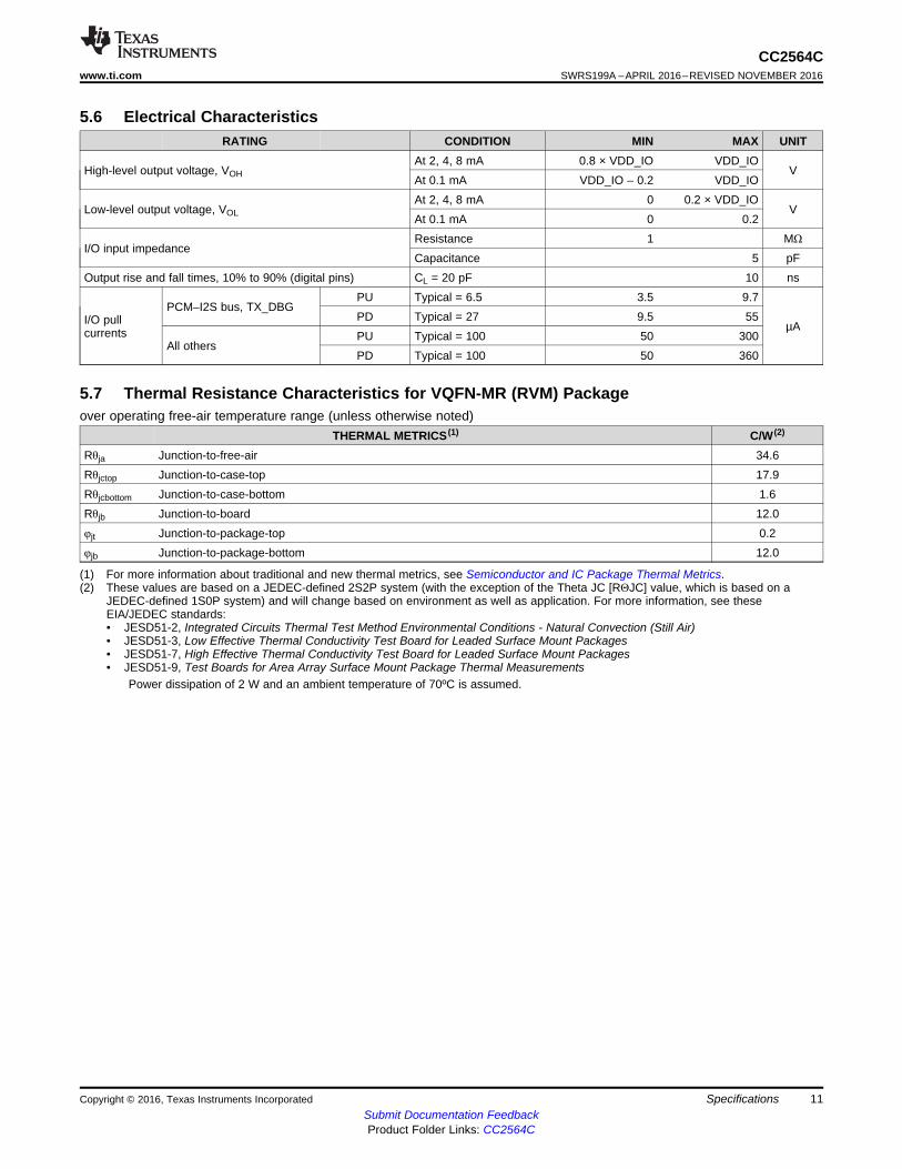
5.6 Electrical CharacteristicsRATING CONDITION MIN MAX UNIT
High-level output voltage, VOHAt 2, 4, 8 mA 0.8 × VDD_IO VDD_IO
VAt 0.1 mA VDD_IO – 0.2 VDD_IO
Low-level output voltage, VOLAt 2, 4, 8 mA 0 0.2 × VDD_IO
VAt 0.1 mA 0 0.2
I/O input impedanceResistance 1 MΩ
Capacitance 5 pFOutput rise and fall times, 10% to 90% (digital pins) CL = 20 pF 10 ns
I/O pullcurrents
PCM–I2S bus, TX_DBGPU Typical = 6.5 3.5 9.7
µAPD Typical = 27 9.5 55
All othersPU Typical = 100 50 300PD Typical = 100 50 360
5.7 Thermal Resistance Characteristics for VQFN-MR (RVM) Package
(1) For more information about traditional and new thermal metrics, see Semiconductor and IC Package Thermal Metrics.(2) These values are based on a JEDEC-defined 2S2P system (with the exception of the Theta JC [RΘJC] value, which is based on a
JEDEC-defined 1S0P system) and will change based on environment as well as application. For more information, see theseEIA/JEDEC standards:• JESD51-2, Integrated Circuits Thermal Test Method Environmental Conditions - Natural Convection (Still Air)• JESD51-3, Low Effective Thermal Conductivity Test Board for Leaded Surface Mount Packages• JESD51-7, High Effective Thermal Conductivity Test Board for Leaded Surface Mount Packages• JESD51-9, Test Boards for Area Array Surface Mount Package Thermal Measurements
Power dissipation of 2 W and an ambient temperature of 70ºC is assumed.
over operating free-air temperature range (unless otherwise noted)THERMAL METRICS (1) C/W (2)
Rθja Junction-to-free-air 34.6Rθjctop Junction-to-case-top 17.9Rθjcbottom Junction-to-case-bottom 1.6Rθjb Junction-to-board 12.0φjt Junction-to-package-top 0.2φjb Junction-to-package-bottom 12.0
12
CC2564CSWRS199A –APRIL 2016–REVISED NOVEMBER 2016 www.ti.com
Submit Documentation FeedbackProduct Folder Links: CC2564C
Specifications Copyright © 2016, Texas Instruments Incorporated
5.8 Timing and Switching Characteristics
5.8.1 Device Power SupplyThe CC2564C power-management hardware and software algorithms provide significant power savings,which is a critical parameter in an MCU-based system.
The power-management module is optimized for drawing extremely low currents.
5.8.1.1 Power Sources
The CC2564C device requires two power sources:• VDD_IN: main power supply for the device• VDD_IO: power source for the 1.8-V I/O ring
The HCI module includes several on-chip voltage regulators for increased noise immunity and can beconnected directly to the battery.
5.8.1.2 Device Power-Up and Power-Down Sequencing
The device includes the following power-up requirements (see Figure 5-1):• nSHUTD must be low. VDD_IN and VDD_IO are don't care I/O pins when nSHUTD is low. However,
signals are not allowed on the I/O pins if I/O power is not supplied, because the I/Os are not fail-safe.Exceptions are SLOW_CLK_IN and AUD_xxx, which are fail-safe and can tolerate external voltageswith no VDD_IO and VDD_IN.
• VDD_IO and VDD_IN must be stable before releasing nSHUTD.• The fast clock must be stable within 20 ms of nSHUTD going high.• The slow clock must be stable within 2 ms of nSHUTD going high.
The device indicates that the power-up sequence is complete by asserting RTS low, which occurs up to100 ms after nSHUTD goes high. If RTS does not go low, the device is not powered up. In this case,ensure that the sequence and requirements are met.
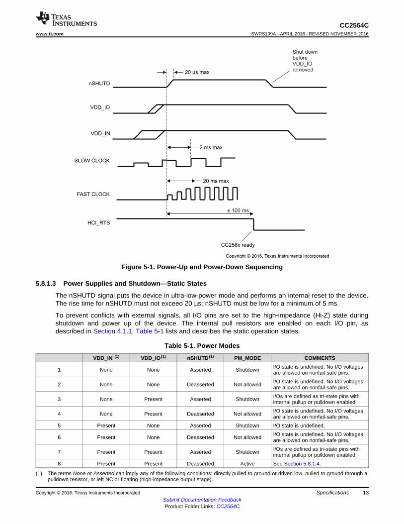
nSHUTD
VDD_IO
HCI_RTS
20 ms max
20 µs max
FAST CLOCK
SLOW CLOCK
CC256x ready
VDD_IN
2 ms max
± 100 ms
Shut downbeforeVDD_IOremoved
Copyright © 2016, Texas Instruments Incorporated
13
CC2564Cwww.ti.com SWRS199A –APRIL 2016–REVISED NOVEMBER 2016
Submit Documentation FeedbackProduct Folder Links: CC2564C
SpecificationsCopyright © 2016, Texas Instruments Incorporated
(1) The terms None or Asserted can imply any of the following conditions: directly pulled to ground or driven low, pulled to ground through apulldown resistor, or left NC or floating (high-impedance output stage).
Figure 5-1. Power-Up and Power-Down Sequencing
5.8.1.3 Power Supplies and Shutdown—Static States
The nSHUTD signal puts the device in ultra-low-power mode and performs an internal reset to the device.The rise time for nSHUTD must not exceed 20 µs; nSHUTD must be low for a minimum of 5 ms.
To prevent conflicts with external signals, all I/O pins are set to the high-impedance (Hi-Z) state duringshutdown and power up of the device. The internal pull resistors are enabled on each I/O pin, asdescribed in Section 4.1.1. Table 5-1 lists and describes the static operation states.
Table 5-1. Power Modes
VDD_IN (1) VDD_IO (1) nSHUTD (1) PM_MODE COMMENTS
1 None None Asserted Shutdown I/O state is undefined. No I/O voltagesare allowed on nonfail-safe pins.
2 None None Deasserted Not allowed I/O state is undefined. No I/O voltagesare allowed on nonfail-safe pins.
3 None Present Asserted Shutdown I/Os are defined as tri-state pins withinternal pullup or pulldown enabled.
4 None Present Deasserted Not allowed I/O state is undefined. No I/O voltagesare allowed on nonfail-safe pins.
5 Present None Asserted Shutdown I/O state is undefined.
6 Present None Deasserted Not allowed I/O state is undefined. No I/O voltagesare allowed on nonfail-safe pins.
7 Present Present Asserted Shutdown I/Os are defined as tri-state pins withinternal pullup or pulldown enabled.
8 Present Present Deasserted Active See Section 5.8.1.4.

14
CC2564CSWRS199A –APRIL 2016–REVISED NOVEMBER 2016 www.ti.com
Submit Documentation FeedbackProduct Folder Links: CC2564C
Specifications Copyright © 2016, Texas Instruments Incorporated
(1) I = input, O = output, Z = Hi-Z, – = no pull, PU = pullup, PD = pulldown, H = high, L = low
5.8.1.4 I/O States in Various Power Modes
CAUTION
Some device I/Os are not fail-safe (see Section 4.1.1). Fail-safe means that thepins do not draw current from an external voltage applied to the pin when I/Opower is not supplied to the device. External voltages are not allowed on theseI/O pins when the I/O supply voltage is not supplied because of possibledamage to the device.
Table 5-2 lists the I/O states in various power modes.
Table 5-2. I/O States in Various Power Modes
I/O NAMESHUTDOWN (1) DEFAULT ACTIVE (1) DEEP SLEEP (1)
I/O State Pull I/O State Pull I/O State PullHCI_RX Z PU I PU I PUHCI_TX Z PU O-H OHCI_RTS Z PU O-H OHCI_CTS Z PU I PU I PUAUD_CLK Z PD I PD I PDAUD_FSYNC Z PD I PD I PDAUD_IN Z PD I PD I PDAUD_OUT Z PD Z PD Z PDTX_DBG Z PU O
5.8.1.5 nSHUTD Requirements
(1) An internal pulldown retains shutdown mode when no external signal is applied to this pin.
PARAMETER MIN MAX UNITVIH Operation mode level (1) 1.42 1.98 VVIL Shutdown mode level (1) 0 0.4 V
Minimum time for nSHUT_DOWN low to reset the device 5 mstr and tf Rise and fall times 20 µs

15
CC2564Cwww.ti.com SWRS199A –APRIL 2016–REVISED NOVEMBER 2016
Submit Documentation FeedbackProduct Folder Links: CC2564C
SpecificationsCopyright © 2016, Texas Instruments Incorporated
5.8.2 Clock Specifications
5.8.2.1 Slow Clock Requirements
An external source must supply the slow clock and connect to the SLOW_CLK_IN pin (for example, thehost or external crystal oscillator). The source must be a digital signal in the range of 0 to 1.8 V. Theaccuracy of the slow-clock frequency must be 32.768 kHz ±250 ppm for Bluetooth use (as specified in theBluetooth specification). The external slow clock must be stable within 64 slow-clock cycles (2 ms)following the release of nSHUTD.
spaceCHARACTERISTICS CONDITION MIN TYP MAX UNITInput slow-clock frequency 32768 HzInput slow-clock accuracy(Initial + temp + aging) Bluetooth ±250 ppm
tr and tfInput transition time tr and tf(10% to 90%) 200 ns
Frequency input duty cycle 15% 50% 85%VIH Slow-clock input voltage limits Square wave,
DC-coupled0.65 × VDD_IO VDD_IO V peak
VIL 0 0.35 × VDD_IO V peakInput impedance 1 MΩ
Input capacitance 5 pF
5.8.2.2 External Fast Clock Crystal Requirements and Operation
spaceCHARACTERISTICS CONDITION MIN TYP MAX UNIT
fin Supported crystal frequencies 26, 38.4 MHz
Frequency accuracy(Initial + temperature + aging) ±20 ppm
Crystal oscillator negative resistance
26 MHz, external capacitance = 8 pF650 940
ΩIosc = 0.5 mA
26 MHz, external capacitance = 20 pF490 710
Iosc = 2.2 mA
10 bits
td_uart_swrs064
t1
HCI_RTS
Start bit Stop bit
HCI_RX
HCI_CTS
HCI_TX
t3 t4
t6
t2
16
CC2564CSWRS199A –APRIL 2016–REVISED NOVEMBER 2016 www.ti.com
Submit Documentation FeedbackProduct Folder Links: CC2564C
Specifications Copyright © 2016, Texas Instruments Incorporated
5.8.2.3 Fast Clock Source Requirements (–40°C to +85°C)
spaceCHARACTERISTICS CONDITION MIN TYP MAX UNIT
Supported frequencies, FREF 26, 38.4 MHzReference frequency accuracy Initial + temp + aging ±20 ppm
Fast-clock input voltage limits
Square wave, DC-coupledVIL –0.2 0.37 VVIH 1.0 2.1 V
Sine wave, AC-coupled 0.4 1.6 Vp-p
Sine wave, DC-coupled 0.4 1.6 Vp-p
Sine wave input limits, DC-coupled 0.0 1.6 VFast-clock input rise time(as % of clock period) Square wave, DC-coupled 10%
Duty cycle 35% 50% 65%
Phase noise for 26 MHz@ offset = 1 kHz –123.4
dBc/Hz@ offset = 10 kHz –133.4@ offset = 100 kHz –138.4
5.8.3 Peripherals
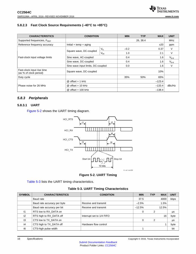
5.8.3.1 UART
Figure 5-2 shows the UART timing diagram.
Figure 5-2. UART Timing
Table 5-3 lists the UART timing characteristics.
Table 5-3. UART Timing Characteristics
SYMBOL CHARACTERISTICS CONDITION MIN TYP MAX UNITBaud rate 37.5 4000 kbpsBaud rate accuracy per byte Receive and transmit –2.5% 1.5%Baud rate accuracy per bit Receive and transmit –12.5% 12.5%
t1 RTS low to RX_DATA on 0 2 µst2 RTS high to RX_DATA off Interrupt set to 1/4 FIFO 16 bytet3 CTS low to TX_DATA on 0 2 µst4 CTS high to TX_DATA off Hardware flow control 1 bytet6 CTS-high pulse width 1 bit
AUD_CLK
AUD_OUT / FSYNC_OUT
AUD_IN / FSYNC_IN
tih
top
tis
Tclk Tw
td_aud_swrs064
Tw
TX STR D0 D1 D2 Dn PAR STP
tb
td_uart_swrs064
17
CC2564Cwww.ti.com SWRS199A –APRIL 2016–REVISED NOVEMBER 2016
Submit Documentation FeedbackProduct Folder Links: CC2564C
SpecificationsCopyright © 2016, Texas Instruments Incorporated
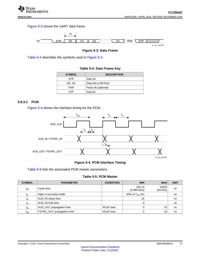
Figure 5-3 shows the UART data frame.
Figure 5-3. Data Frame
Table 5-4 describes the symbols used in Figure 5-3.
Table 5-4. Data Frame Key
SYMBOL DESCRIPTIONSTR Start bit
D0...Dn Data bits (LSB first)PAR Parity bit (optional)STP Stop bit
5.8.3.2 PCM
Figure 5-4 shows the interface timing for the PCM.
Figure 5-4. PCM Interface Timing
Table 5-5 lists the associated PCM master parameters.
Table 5-5. PCM Master
SYMBOL PARAMETER CONDITION MIN MAX UNIT
tclk Cycle time 244.14(4.096 MHz)
15625(64 kHz) ns
tw High or low pulse width 50% of Tclk min nstis AUD_IN setup time 25 nstih AUD_IN hold time 0 nstop AUD_OUT propagation time 40-pF load 0 10 nstop FSYNC_OUT propagation time 40-pF load 0 10 ns

18
CC2564CSWRS199A –APRIL 2016–REVISED NOVEMBER 2016 www.ti.com
Submit Documentation FeedbackProduct Folder Links: CC2564C
Specifications Copyright © 2016, Texas Instruments Incorporated
Table 5-6 lists the associated PCM slave parameters.
Table 5-6. PCM Slave
SYMBOL PARAMETER CONDITION MIN MAX UNIT
tclk Cycle time 66.67(15 MHz) ns
tw High or low pulse width 40% of Tclk nsTis AUD_IN setup time 8 nstih AUD_IN hold time 0 nstis AUD_FSYNC setup time 8 nstih AUD_FSYNC hold time 0 nstop AUD_OUT propagation time 40-pF load 0 21 ns
19
CC2564Cwww.ti.com SWRS199A –APRIL 2016–REVISED NOVEMBER 2016
Submit Documentation FeedbackProduct Folder Links: CC2564C
SpecificationsCopyright © 2016, Texas Instruments Incorporated
(1) Sensitivity degradation up to 3 dB may occur for minimum and typical values where the Bluetooth frequency is a harmonic of the fastclock.
(2) Numbers show ratio of desired signal to interfering signal. Smaller numbers indicate better C/I performance.
5.8.4 RF Performance
5.8.4.1 Bluetooth® BR and EDR RF Performance
All parameters in this section that are fast-clock dependent are verified using a 26-MHz XTAL and38.4-MHz TCXO.
5.8.4.1.1 Bluetooth® Receiver—In-Band Signals
CHARACTERISTICS CONDITION MIN TYP MAX BLUETOOTHSPECIFICATION UNIT
Operation frequency range 2402 2480 MHz
Channel spacing 1 MHz
Input impedance 50 Ω
Sensitivity, dirty TX on (1)
GFSK, BER = 0.1% –91.5 –95 –70
dBmπ/4-DQPSK, BER = 0.01% –90.5 –94.5 –70
8DPSK, BER = 0.01% –81 –87.5 –70
BER error floor at sensitivity +10 dB, dirty TX off
π/4-DQPSK 1E–6 1E–7 1E–5
8DPSK 1E–6 1E–5
Maximum usable input power
GFSK, BER = 0.1% –5 –20
dBmπ/4-DQPSK, BER = 0.1% –10
8DPSK, BER = 0.1% –10
Intermodulation characteristics Level of interferers (for n = 3, 4, and 5) –36 –30 –39 dBm
C/I performance (2)
Image = –1 MHz
GFSK, cochannel 8 10 11
dB
EDR, cochannelπ/4-DQPSK 9.5 11 13
8DPSK 16.5 20 21
GFSK, adjacent ±1 MHz –10 –5 0
EDR, adjacent ±1 MHz, (image)π/4-DQPSK –10 –5 0
8DPSK –5 –1 5
GFSK, adjacent +2 MHz –38 –35 –30
EDR, adjacent, +2 MHzπ/4-DQPSK –38 –35 –30
8DPSK –38 –30 –25
GFSK, adjacent –2 MHz –28 –20 –20
EDR, adjacent –2 MHzπ/4-DQPSK –28 –20 –20
8DPSK –22 –13 –13
GFSK, adjacent ≥ |±3| MHz –45 –43 –40
EDR, adjacent ≥ |±3| MHzπ/4-DQPSK –45 –43 –40
8DPSK –44 –36 –33
RF return loss –10 dB
RX mode LO leakage Frf = (received RF – 0.6 MHz) –63 –58 dBm
(1) Exceptions are taken out of the total 24 allowed in the Bluetooth specification.
5.8.4.1.2 Bluetooth® Receiver—General Blocking
CHARACTERISTICS CONDITION MIN TYP UNIT
Blocking performance over full range, according to Bluetoothspecification (1)
30 to 2000 MHz –6
dBm2000 to 2399 MHz –62484 to 3000 MHz –63 to 12.75 GHz –6

20
CC2564CSWRS199A –APRIL 2016–REVISED NOVEMBER 2016 www.ti.com
Submit Documentation FeedbackProduct Folder Links: CC2564C
Specifications Copyright © 2016, Texas Instruments Incorporated
(1) To modify maximum output power, use an HCI VS command.
5.8.4.1.3 Bluetooth® Transmitter—GFSK
CHARACTERISTICS MIN TYP MAX BLUETOOTHSPECIFICATION UNIT
Maximum RF outputpower (1)
VDD_IN = VBAT 12dBm
VDD_IN = external regulator to 1.8 V 10Power variation over Bluetooth band –1 1 dBGain control range 30 dBPower control step 5 2 to 8 dBAdjacent channel power |M–N| = 2 –45 ≤ –20 dBmAdjacent channel power |M–N| > 2 –50 ≤ –40 dBm
(1) To modify maximum output power, use an NCI VS command.
5.8.4.1.4 Bluetooth® Transmitter—EDR
CHARACTERISTICS MIN TYP MAX BLUETOOTHSPECIFICATION UNIT
EDR outputpower (1)
π/4-DQPSKVDD_IN = VBAT 5.5
dBmVDD_IN = external regulator to 1.8 V 5.5
8DPSKVDD_IN = VBAT 5.5VDD_IN = external regulator to 1.8 V 5.5
EDR relative power –2 1 –4 to +1 dBPower variation over Bluetooth band –1 1 dBGain control range 30 dBPower control step 5 2 to 8 dBAdjacent channel power |M–N| = 1 –36 ≤ –26 dBcAdjacent channel power |M–N| = 2 –30 ≤ –20 dBmAdjacent channel power |M–N| > 2 –42 ≤ –40 dBm
5.8.4.1.5 Bluetooth® Modulation—GFSK
CHARACTERISTICS CONDITION MIN TYP MAX BLUETOOTHSPECIFICATION UNIT
–20-dB bandwidth GFSK 925 ≤ 1000 kHz
F1 avg
Modulation characteristics
Δf1avgMod data = 4 1 s,4 0 s:111100001111...
165 140 to 175 kHz
F2 max
Δf2max ≥ limit for atleast 99.9% of allΔf2max
Mod data = 1010101... 130 > 115 kHz
Δf2avg, Δf1avg 88% > 80%
Absolute carrier frequencydrift
DH1 –25 25 < ±25kHz
DH3 and DH5 –35 35 < ±40
Drift rate 15 < 20 kHz/50 µs
Initial carrier frequencytolerance f0–fTX –75 +75 < ±75 kHz

21
CC2564Cwww.ti.com SWRS199A –APRIL 2016–REVISED NOVEMBER 2016
Submit Documentation FeedbackProduct Folder Links: CC2564C
SpecificationsCopyright © 2016, Texas Instruments Incorporated
(1) Maximum performance refers to maximum TX power.
5.8.4.1.6 Bluetooth® Modulation—EDR
CHARACTERISTICS CONDITION MIN TYP MAX BLUETOOTHSPECIFICATION UNIT
Carrier frequency stability ±5 ≤ 10 kHzInitial carrier frequency tolerance ±75 ±75 kHz
RMS DEVM (1) π/4-DQPSK 6% 20%8DPSK 6% 13%
99% DEVM (1) π/4-DQPSK 30% 30%8DPSK 20% 20%
Peak DEVM (1) π/4-DQPSK 14% 35%8DPSK 16% 25%
(1) Meets FCC and ETSI requirements with external filter shown in Figure 7-1.
5.8.4.1.7 Bluetooth® Transmitter—Out-of-Band and Spurious Emissions
CHARACTERISTICS CONDITION TYP MAX UNITSecond harmonic (1)
Measured at maximum output power–14 –2 dBm
Third harmonic (1) –10 –6 dBmFourth harmonics (1) –19 –11 dBm
(1) Sensitivity degradation up to 3 dB may occur where the Bluetooth low energy frequency is a harmonic of the fast clock.(2) Numbers show wanted signal-to-interfering signal ratio. Smaller numbers indicate better C/I performance.
5.8.4.2 Bluetooth® low energy RF Performance
All parameters in this section that are fast-clock dependent are verified using a 26-MHz XTAL and a38.4-MHz TCXO.
5.8.4.2.1 Bluetooth® low energy Receiver—In-Band Signals
CHARACTERISTIC CONDITION MIN TYP MAXBLUETOOTHlow energy
SPECIFICATIONUNIT
Operation frequency range 2402 2480 MHzChannel spacing 2 MHzInput impedance 50 Ω
Sensitivity, dirty TX on (1) PER = 30.8%; dirty TX on –96 ≤ –70 dBmMaximum usable input power GMSK, PER = 30.8% –5 ≥ –10 dBm
Intermodulation characteristics Level of interferers(for n = 3, 4, 5) –30 ≥ –50 dBm
C/I performance (2)
Image = –1 MHz
GMSK, cochannel 8 ≤ 21
dBGMSK, adjacent ±1 MHz –5 ≤ 15GMSK, adjacent +2 MHz –45 ≤ –17GMSK, adjacent –2 MHz –22 ≤ –15GMSK, adjacent ≥ |±3| MHz –47 ≤ –27
RX mode LO leakage Frf = (received RF – 0.6 MHz) –63 dBm
22
CC2564CSWRS199A –APRIL 2016–REVISED NOVEMBER 2016 www.ti.com
Submit Documentation FeedbackProduct Folder Links: CC2564C
Specifications Copyright © 2016, Texas Instruments Incorporated
(1) Exceptions are taken out of the total 10 allowed in the Bluetooth low energy specification.
5.8.4.2.2 Bluetooth® low energy Receiver—General Blocking
CHARACTERISTICS CONDITION MIN TYPBLUETOOTHlow energy
SPECIFICATIONUNIT
Blocking performance over fullrange, according to Bluetoothlow energy specification (1)
30 to 2000 MHz –15 ≥ –30
dBm2000 to 2399 MHz –15 ≥ –352484 to 3000 MHz –15 ≥ –353 to 12.75 GHz –15 ≥ –30
(1) To achieve the Bluetooth low energy specification of 10-dBm maximum, an insertion loss of > 2 dB is assumed between the RF ball andthe antenna. Otherwise, use an HCI VS command to modify the output power.
5.8.4.2.3 Bluetooth® low energy Transmitter
CHARACTERISTICS MIN TYP MAXBLUETOOTHlow energy
SPECIFICATIONUNIT
RF output powerVDD_IN = VBAT 12 (1) ≤10
dBmVDD_IN = External regulator to 1.8 V 10 ≤10
Power variation over Bluetooth low energy band 1 dBAdjacent channel power |M-N| = 2 –45 ≤ –20 dBmAdjacent channel power |M-N| > 2 –50 ≤ –30 dBm
5.8.4.2.4 Bluetooth® low energy Modulation
CHARACTERISTICS CONDITION MIN TYP MAXBLUETOOTHlow energy
SPECIFICATIONUNIT
Δf1 avg
Modulationcharacteristics
Δf1avg Mod data = 4 1s, 4 0 s:1111000011110000... 240 250 260 225 to 275 kHz
Δf2 max
Δf2max ≥ limit for atleast 99.9% of allΔf2max
Mod data = 1010101... 185 210 ≥ 185 kHz
Δf2avg, Δf1avg 0.85 0.9 ≥ 0.8Absolute carrierfrequency drift –25 25 ≤ ±50 kHz
Drift rate 15 ≤ 20 kHz/50 msInitial carrierfrequencytolerance
–75 75 ≤ ±100 kHz
(1) Meets FCC and ETSI requirements with external filter shown in Figure 7-1.
5.8.4.2.5 Bluetooth® low energy Transceiver, Out-Of-Band and Spurious Emissions
CHARACTERISTICS CONDITION TYP MAX UNITSecond harmonic (1)
Measured at maximum output power–14 –2 dBm
Third harmonic (1) –10 –6 dBmFourth harmonics (1) –19 –11 dBm

PCM-I2S
UART
CC2564C
I/Ointerface
Coprocessor(See Note)
BR/EDRmain processor
Modemarbitrator
DRP
Powermanagement
Clockmanagement
2.4-GHzband-pass filter
HCI
Slowclock
Fastclock
Power Shutdown
Copyright © 2016, Texas Instruments Incorporated
23
CC2564Cwww.ti.com SWRS199A –APRIL 2016–REVISED NOVEMBER 2016
Submit Documentation FeedbackProduct Folder Links: CC2564C
Detailed DescriptionCopyright © 2016, Texas Instruments Incorporated
6 Detailed Description
6.1 OverviewThe CC2564C architecture comprises a DRP and a point-to-multipoint baseband core. The architecture isbased on a single-processor ARM7TDMI® core. The device includes several on-chip peripherals to enableeasy communication with a host system and the Bluetooth BR, EDR, and low energy core.
6.2 Functional Block Diagram
NOTE: The following technologies and assisted modes cannot be used simultaneously with the coprocessor: Bluetooth lowenergy, assisted HFP 1.6 (WBS), and assisted A2DP. Only one technology or assisted mode can be used at a time.
Figure 6-1. CC2564C Functional Block Diagram
6.3 Clock InputsThis section describes the available clock inputs. For specifications, see Section 5.8.2.
6.3.1 Slow ClockAn external source must supply the slow clock and connect to the SLOW_CLK_IN pin (for example, thehost or external crystal oscillator). The source must be a digital signal in the range of 0 V to 1.8 V. Theaccuracy of the slow-clock frequency must be 32.768 kHz ±250 ppm for Bluetooth use (as specified in theBluetooth specification). The external slow clock must be stable within 64 slow-clock cycles (2 ms)following the release of nSHUTD.
6.3.2 Fast Clock Using External Clock SourceAn external clock source is fed to an internal pulse-shaping cell to provide the fast-clock signal for thedevice. The device incorporates an internal, automatic clock-scheme detection mechanism thatautomatically detects the fast-clock scheme used and configures the FREF cell accordingly. Thismechanism ensures that the electrical characteristics (loading) of the fast-clock input remain staticregardless of the scheme used and eliminates any power-consumption penalty-versus-scheme used.
The frequency variation of the fast-clock source must not exceed ±20 ppm (as defined by the Bluetoothspecification).
The external clock can be AC- or DC-coupled, sine or square wave.

FREFP
FREFM
CC2564C
VDD_IO
Copyright © 2016, Texas Instruments Incorporated
–0.2
V [V]Fref
Vhigh_min
t
2.1
1.0
Vlow_max0.37
clksqtd_wrs064
FREFP
FREFM
CC2564C
Copyright © 2016, Texas Instruments Incorporated
24
CC2564CSWRS199A –APRIL 2016–REVISED NOVEMBER 2016 www.ti.com
Submit Documentation FeedbackProduct Folder Links: CC2564C
Detailed Description Copyright © 2016, Texas Instruments Incorporated
6.3.2.1 External FREF DC-Coupled
Figure 6-2 and Figure 6-3 show the clock configuration when using a square wave, DC-coupled externalsource for the fast-clock input.
NOTEA shunt capacitor with a range of 10 nF must be added on the oscillator output to reject highharmonics and shape the signal to be close to a sinusoidal waveform.
TI recommends using only a dedicated LDO to feed the oscillator. Do not use the same VIOfor the oscillator and the CC2564C device.
Figure 6-2. Clock Configuration (Square Wave, DC-Coupled)
Figure 6-3. External Fast Clock (Square Wave, DC-Coupled)
Figure 6-4 and Figure 6-5 show the clock configuration when using a sine wave, DC-coupled externalsource for the fast clock input.
Figure 6-4. Clock Configuration (Sine Wave, DC-Coupled)

t
1 V
0.8
0.2
0
–0.2
–0.8
V [V]IN
VPP = 0.4 – 1.6 Vp-p
SWRS097-022
FREFP
FREFM
CC2564C
VDD_IO
68 pF
Copyright © 2016, Texas Instruments Incorporated
t
VIN
1.6 V
0
V = 0.2 – 1.4 Vdc
VPP = 0.4 – 1.6 Vp-p
SWRS097-023
25
CC2564Cwww.ti.com SWRS199A –APRIL 2016–REVISED NOVEMBER 2016
Submit Documentation FeedbackProduct Folder Links: CC2564C
Detailed DescriptionCopyright © 2016, Texas Instruments Incorporated
Figure 6-5. External Fast Clock (Sine Wave, DC-Coupled)
6.3.2.2 External FREF Sine Wave, AC-Coupled
Figure 6-6 and Figure 6-7 show the configuration when using a sine wave, AC-coupled external source forthe fast-clock input.
Figure 6-6. Clock Configuration (Sine Wave, AC-Coupled)
Figure 6-7. External Fast Clock (Sine Wave, AC-Coupled)
In cases where the input amplitude is greater than 1.6 Vp-p, the amplitude can be reduced to within limits.Using a small series capacitor forms a voltage divider with the internal input capacitance of approximately2 pF to provide the required amplitude at the device input.

Oscillatorbuffer
CC2564C
XTALM
XTALP
XTAL
C1
C2
Copyright © 2016, Texas Instruments Incorporated
26
CC2564CSWRS199A –APRIL 2016–REVISED NOVEMBER 2016 www.ti.com
Submit Documentation FeedbackProduct Folder Links: CC2564C
Detailed Description Copyright © 2016, Texas Instruments Incorporated
6.3.2.3 Fast Clock Using External Crystal
The CC2564C device incorporates an internal crystal oscillator buffer to support a crystal-based fast-clockscheme. The supported crystal frequencies are 26 and 38.4 MHz.
The frequency accuracy of the fast-clock source must not exceed ±20 ppm (including the accuracy of thecapacitors, as specified in the Bluetooth specification).
Figure 6-8 shows the recommended fast-clock circuitry.
Figure 6-8. Fast-Clock Crystal Circuit
Table 6-1 lists component values for the fast-clock crystal circuit.
(1) To achieve the required accuracy, values for C1 and C2 must betaken from the crystal manufacturer's data sheet and layoutconsiderations.
Table 6-1. Fast-Clock Crystal CircuitComponent Values
FREQ (MHz) C1 (pF) (1) C2 (pF) (1)
26 12 12

TX digital data
RX digital data
Digital
Demodulation
Amplitude
PhaseADPLL
FilterADC IFA LNA
Transmitter path
Receiver path
SWRS092-005
DPA
Copyright © 2016, Texas Instruments Incorporated
27
CC2564Cwww.ti.com SWRS199A –APRIL 2016–REVISED NOVEMBER 2016
Submit Documentation FeedbackProduct Folder Links: CC2564C
Detailed DescriptionCopyright © 2016, Texas Instruments Incorporated
6.4 Functional Blocks
6.4.1 RFThe CC2564C device is the third generation of Bluetooth single-chip devices using DRP architecture fromTI. Modifications and new features added to the DRP further improve radio performance.
Figure 6-9 shows the DRP block diagram.
Figure 6-9. DRP Block Diagram
6.4.1.1 Receiver
The receiver uses near-zero-IF architecture to convert the RF signal to baseband data. The signalreceived from the external antenna is input to a single-ended low-noise amplifier (LNA) and passed to amixer that downconverts the signal to IF, followed by a filter and amplifier. The signal is then quantized bya sigma-delta analog-to-digital converter (ADC) and further processed to reduce the interference level.
The demodulator digitally downconverts the signal to zero-IF and recovers the data stream using anadaptive-decision mechanism. The demodulator includes EDR processing with:• State-of-the-art performance• A maximum-likelihood sequence estimator (MLSE) to improve the performance of basic-rate GFSK
sensitivity• Adaptive equalization to enhance EDR modulation
New features include:• LNA input range narrowed to increase blocking performance• Active spur cancellation to increase robustness to spurs

28
CC2564CSWRS199A –APRIL 2016–REVISED NOVEMBER 2016 www.ti.com
Submit Documentation FeedbackProduct Folder Links: CC2564C
Detailed Description Copyright © 2016, Texas Instruments Incorporated
6.4.1.2 Transmitter
The transmitter is an all-digital, sigma-delta phase-locked loop (ADPLL) based with a digitally controlledoscillator (DCO) at 2.4 GHz as the RF clock. The transmitter directly modulates the digital PLL. The poweramplifier is also digitally controlled. The transmitter uses the polar-modulation technique. While the phase-modulated control word is fed to the ADPLL, the amplitude-modulated controlled word is fed to the class-Eamplifier to generate a Bluetooth standard-compliant RF signal.
New features include:• Improved TX output power• LMS algorithm to improve the differential error vector magnitude (DEVM)
6.4.2 Host Controller InterfaceThe CC2564C device incorporates one UART module dedicated to the HCI transport layer. The HCItransports commands, events, and ACL between the device and the host using HCI data packets.
The CC2564C device supports the H4 protocol (4-wire UART) with hardware flow control and the H5protocol (3-wire UART) with software flow control. The CC2564C device automatically detects the protocolon reception of the first command.
The maximum baud rate of the UART module is 4 Mbps; however, the default baud rate after power up isset to 115.2 kbps. The baud rate can thereafter be changed with a VS command. The device respondswith a command complete event (still at 115.2 kbps), after which the baud rate change occurs.
The UART module includes the following features:• Receiver detection of break, idle, framing, FIFO overflow, and parity error conditions• Transmitter underflow detection• CTS and RTS hardware flow control (H4 protocol)• XON and XOFF software flow control (H5 protocol)
Table 6-2 lists the UART module default settings.
Table 6-2. UART Module Default Settings
PARAMETER VALUEBit rate 115.2 kbps
Data length 8 bitsStop bit 1Parity None

Host CC2564C
Host_RX
Host_TX
Host_CTS
Host_RTS
HCI_RX
HCI_TX
HCI_CTS
HCI_RTS
Copyright © 2016, Texas Instruments Incorporated
29
CC2564Cwww.ti.com SWRS199A –APRIL 2016–REVISED NOVEMBER 2016
Submit Documentation FeedbackProduct Folder Links: CC2564C
Detailed DescriptionCopyright © 2016, Texas Instruments Incorporated
6.4.2.1 4-Wire UART Interface—H4 Protocol
The H4 UART Interface includes four signals:• TX• RX• CTS• RTS
Flow control between the host and the CC2564C device is bytewise by hardware.
Figure 6-10 shows the H4 UART interface.
Figure 6-10. H4 UART Interface
When the UART RX buffer of the device passes the flow control threshold, it sets the HCI_RTS signalhigh to stop transmission from the host.
When the HCI_CTS signal is set high, the device stops transmission on the interface. If HCI_CTS is sethigh while transmitting a byte, the device finishes transmitting the byte and stops the transmission.
The H4 protocol device includes a mechanism that handles the transition between active mode and sleepmode. The protocol occurs through the CTS and RTS UART lines and is known as the enhanced HCI lowlevel (eHCILL) power-management protocol.
For more information on the H4 UART protocol, see Volume 4 Host Controller Interface, Part A UARTTransport Layer of the Bluetooth Core Specifications(www.bluetooth.org/en-us/specification/adoptedspecifications).
Host CC2564C
Host_RX
Host_TX
HCI_RX
HCI_TX
GND GND
Copyright © 2016, Texas Instruments Incorporated
30
CC2564CSWRS199A –APRIL 2016–REVISED NOVEMBER 2016 www.ti.com
Submit Documentation FeedbackProduct Folder Links: CC2564C
Detailed Description Copyright © 2016, Texas Instruments Incorporated
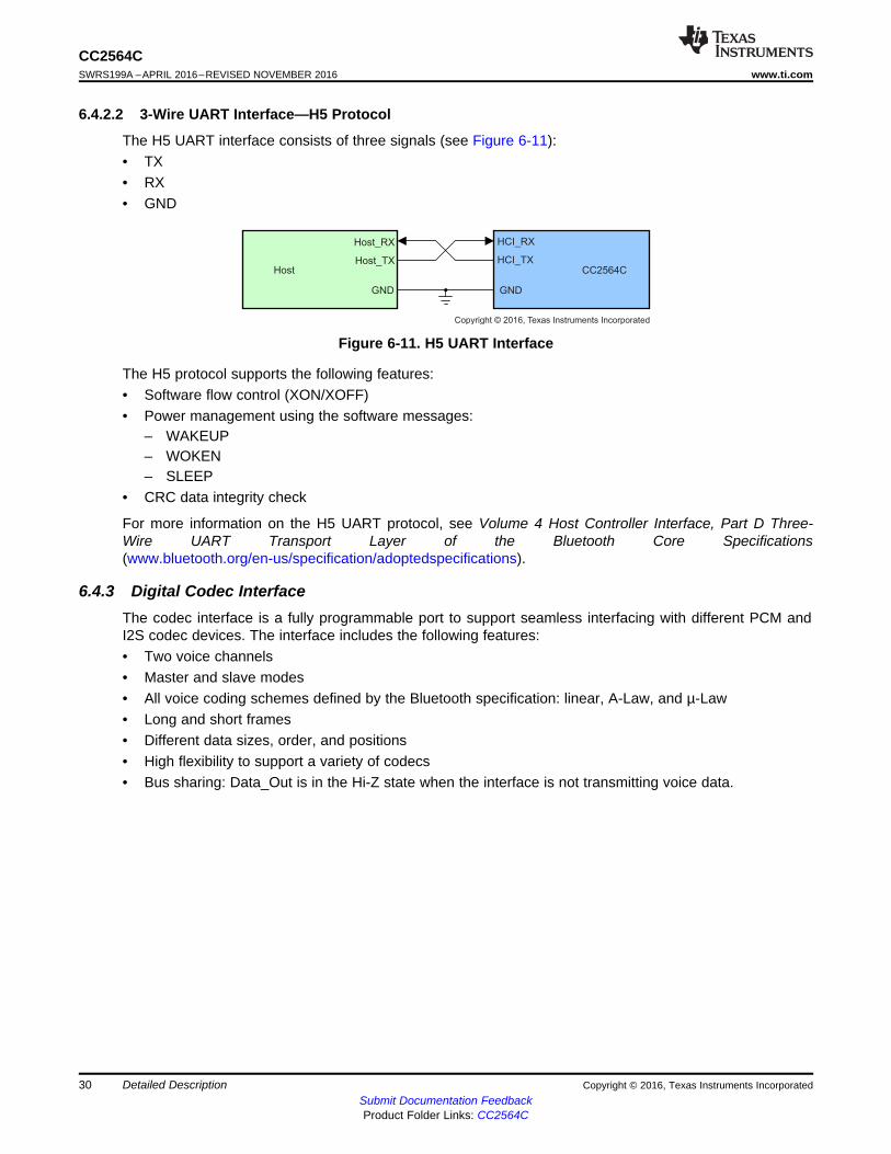
6.4.2.2 3-Wire UART Interface—H5 Protocol
The H5 UART interface consists of three signals (see Figure 6-11):• TX• RX• GND
Figure 6-11. H5 UART Interface
The H5 protocol supports the following features:• Software flow control (XON/XOFF)• Power management using the software messages:
– WAKEUP– WOKEN– SLEEP
• CRC data integrity check
For more information on the H5 UART protocol, see Volume 4 Host Controller Interface, Part D Three-Wire UART Transport Layer of the Bluetooth Core Specifications(www.bluetooth.org/en-us/specification/adoptedspecifications).
6.4.3 Digital Codec InterfaceThe codec interface is a fully programmable port to support seamless interfacing with different PCM andI2S codec devices. The interface includes the following features:• Two voice channels• Master and slave modes• All voice coding schemes defined by the Bluetooth specification: linear, A-Law, and µ-Law• Long and short frames• Different data sizes, order, and positions• High flexibility to support a variety of codecs• Bus sharing: Data_Out is in the Hi-Z state when the interface is not transmitting voice data.

31
CC2564Cwww.ti.com SWRS199A –APRIL 2016–REVISED NOVEMBER 2016
Submit Documentation FeedbackProduct Folder Links: CC2564C
Detailed DescriptionCopyright © 2016, Texas Instruments Incorporated
6.4.3.1 Hardware Interface
The interface includes four signals:• Clock: configurable direction (input or output)• Frame_Sync and Word_Sync: configurable direction (input or output)• Data_In: input• Data_Out: output or tri-state signal
The CC2564C device can be the master of the interface when generating the Clock and Frame_Syncsignals or the slave when receiving these two signals.
For slave mode, clock input frequencies of up to 15 MHz are supported. At clock rates above 12 MHz, themaximum data burst size is 32 bits.
For master mode, the device can generate any clock frequency from 64 kHz to 4.096 MHz.
6.4.3.2 I2S
When the codec interface is configured to support the I2S protocol, these settings are recommended:• Bidirectional, full-duplex interface• Two time slots per frame: time slot 0 for the left channel audio data; and time slot 1 for the right
channel audio data• The length of each time slot is configurable up to 40 serial clock cycles, and the length of the frame is
configurable up to 80 serial clock cycles
6.4.3.3 Data Format
The data format is fully configurable:• The data length can be from 8 to 320 bits in 1-bit increments when working with 2 channels, or up to
640 bits when working with 1 channel. The data length can be set independently for each channel.• The data position within a frame is also configurable within 1 clock (bit) resolution and can be set
independently (relative to the edge of the Frame_Sync signal) for each channel.• The Data_In and Data_Out bit order can be configured independently. For example; Data_In can start
with the most significant bit (MSB); Data_Out can start with the least significant bit (LSB). Eachchannel is separately configurable. The inverse bit order (that is, LSB first) is supported only forsample sizes up to 24 bits.
• Data_In and Data_Out are not required to be the same length.• The Data_Out line is configured to Hi-Z output between data words. Data_Out can also be set for
permanent Hi-Z output, regardless of the data output. This configuration allows the device to be a busslave in a multislave PCM environment. At power up, Data_Out is configured as Hi-Z output.
6.4.3.4 Frame-Idle Period
The codec interface handles frame-idle periods, during which the clock pauses and becomes 0 at the endof the frame after all data are transferred.
The device supports frame-idle periods both as master and slave of the codec bus.
When the device is the master of the interface, the frame-idle period is configurable. There are twoconfigurable parameters:• Clk_Idle_Start: indicates the number of clock cycles from the beginning of the frame to the beginning of
the frame-idle period. After Clk_Idle_Start clock cycles, the clock becomes 0.• Clk_Idle_End: indicates the time from the beginning of the frame to the end of the frame-idle period.
The time is given in multiples of clock periods.
The delta between Clk_Idle_Start and Clk_Idle_End is the clock idle period.
For example, for clock rate = 1 MHz, frame sync period = 10 kHz, Clk_Idle_Start = 60, Clk_Idle_End = 90.

PCM FSYNC
CC256x
SAMPLE TIME
PCM DATA IN
PCM CLK
D7 D3D5 D4 D2 D1 D0D6
SWRS121-004
Copyright © 2016, Texas Instruments Incorporated
Clock
Data_In
Frame_Sync
Frame period
Data_OutFrame idle
Clk_Idle_Start
Clk_Idle_End
frmidle_swrs064
32
CC2564CSWRS199A –APRIL 2016–REVISED NOVEMBER 2016 www.ti.com
Submit Documentation FeedbackProduct Folder Links: CC2564C
Detailed Description Copyright © 2016, Texas Instruments Incorporated
Between both Frame_Sync signals there are 70 clock cycles (instead of 100). The clock idle period starts60 clock cycles after the beginning of the frame and lasts 90 – 60 = 30 clock cycles. Thus, the idle periodends 100 – 90 = 10 clock cycles before the end of the frame. The data transmission must end before thebeginning of the idle period.
Figure 6-12 shows the frame idle timing.
Figure 6-12. Frame Idle Period
6.4.3.5 Clock-Edge Operation
The codec interface of the device can work on the rising or the falling edge of the clock and can samplethe Frame_Sync signal and the data at inversed polarity.
Figure 6-13 shows the operation of a falling-edge-clock type of codec. The codec is the master of the bus.The Frame_Sync signal is updated (by the codec) on the falling edge of the clock and is thereforesampled (by the device) on the next rising clock. The data from the codec is sampled (by the device) onthe falling edge of the clock.
Figure 6-13. Negative Clock Edge Operation
6.4.3.6 Two-Channel Bus Example
Figure 6-14 shows a 2-channel bus in which the two channels have different word sizes and arbitrarypositions in the bus frame.

...
Fsync
Data_Out
Data_In
...
Clock
FT
MSB LSB MSB LSB
PCM_data_window
CH1 data start FT = 0 CH1 data length = 11 CH2 datastart FT = 43
CH2 datalength = 8
Fsync period = 128Fsync length = 1
...
...
......
twochpcm_swrs064
9876543210127 42 43 44 0127
bit0
bit1
bit2
bit3
bit4
bit5
bit6
bit7
bit8
bit9
bit10
bit0
bit1
bit2
bit3
bit4
bit5
bit6
bit7
bit0
bit1
bit2
bit3
bit4
bit5
bit6
bit7
bit8
bit9
bit10
bit0
bit1
bit2
bit3
bit4
bit5
bit6
bit7
33
CC2564Cwww.ti.com SWRS199A –APRIL 2016–REVISED NOVEMBER 2016
Submit Documentation FeedbackProduct Folder Links: CC2564C
Detailed DescriptionCopyright © 2016, Texas Instruments Incorporated
NOTE: FT stands for frame timer.
Figure 6-14. 2-Channel Bus Timing
6.4.4 Assisted ModesThe CC2564C device contains an embedded coprocessor that can be used for multiple purposes (seeFigure 1-1). The CC2564C device uses the coprocessor to perform the LE functionality or to execute theassisted HFP 1.6 (WBS) or assisted A2DP functions. Only one of these functions can be executed at atime because they all use the same resources (that is, the coprocessor; see Table 3-1 for the modes ofoperation supported by each device).
This section describes the assisted HFP 1.6 (WBS) and assisted A2DP modes of operation. These modesof operation minimize host processing and power by taking advantage of the device coprocessor toperform the voice and audio SBC processing required in HFP 1.6 (WBS) and A2DP profiles. This sectionalso compares the architecture of the assisted modes with the common implementation of the HFP 1.6and A2DP profiles.
The assisted HFP 1.6 (WBS) and assisted A2DP modes of operation comply fully with the HFP 1.6 andA2DP Bluetooth specifications. For more information on these profiles, see the corresponding BluetoothProfile Specification (www.bluetooth.org/en-us/specification/adopted-specifications).
6.4.4.1 Assisted HFP 1.6 (WBS)
The HFP 1.6 Profile Specification adds the requirement for WBS support. The WBS feature allows twicethe voice quality versus legacy voice coding schemes at the same air bandwidth (64 kbps). This feature isachieved using a voice sampling rate of 16 kHz, a modified subband coding (mSBC) scheme, and apacket loss concealment (PLC) algorithm. The mSBC scheme is a modified version of the mandatoryaudio coding scheme used in the A2DP profile with the parameters listed in Table 6-3.
Table 6-3. mSBC Parameters
PARAMETER VALUEChannel mode MonoSampling rate 16 kHzAllocation method LoudnessSubbands 8Block length 15Bitpool 26
Host Processor
Bluetooth Stack
CC256xBluetooth Controller
HCI
HCI
Control
HFP1.6Profile
Audio codec
Data
Control
16 kHz16 bits
HFP 1.6 Architecture Assisted HFP 1.6 Architecture
SCO
L2CAP
Data
PCM/
I2S
mSBC + PLC
Host Processor
Bluetooth Stack
CC256xBluetooth Controller
HCI
HCI
Control
HFP1.6Profile
Audio codec
Data
Control
16 kHz16 bits
L2CAP
PCM/
I2S
mSBC + PLC
Copyright © 2016, Texas Instruments Incorporated
34
CC2564CSWRS199A –APRIL 2016–REVISED NOVEMBER 2016 www.ti.com
Submit Documentation FeedbackProduct Folder Links: CC2564C
Detailed Description Copyright © 2016, Texas Instruments Incorporated
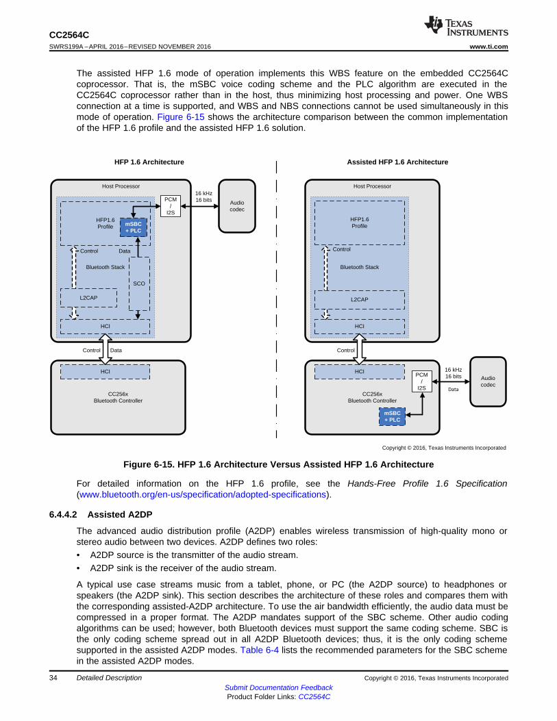
The assisted HFP 1.6 mode of operation implements this WBS feature on the embedded CC2564Ccoprocessor. That is, the mSBC voice coding scheme and the PLC algorithm are executed in theCC2564C coprocessor rather than in the host, thus minimizing host processing and power. One WBSconnection at a time is supported, and WBS and NBS connections cannot be used simultaneously in thismode of operation. Figure 6-15 shows the architecture comparison between the common implementationof the HFP 1.6 profile and the assisted HFP 1.6 solution.
Figure 6-15. HFP 1.6 Architecture Versus Assisted HFP 1.6 Architecture
For detailed information on the HFP 1.6 profile, see the Hands-Free Profile 1.6 Specification(www.bluetooth.org/en-us/specification/adopted-specifications).
6.4.4.2 Assisted A2DP
The advanced audio distribution profile (A2DP) enables wireless transmission of high-quality mono orstereo audio between two devices. A2DP defines two roles:• A2DP source is the transmitter of the audio stream.• A2DP sink is the receiver of the audio stream.
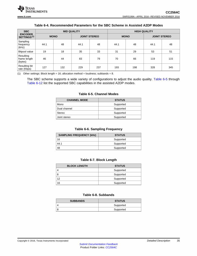
A typical use case streams music from a tablet, phone, or PC (the A2DP source) to headphones orspeakers (the A2DP sink). This section describes the architecture of these roles and compares them withthe corresponding assisted-A2DP architecture. To use the air bandwidth efficiently, the audio data must becompressed in a proper format. The A2DP mandates support of the SBC scheme. Other audio codingalgorithms can be used; however, both Bluetooth devices must support the same coding scheme. SBC isthe only coding scheme spread out in all A2DP Bluetooth devices; thus, it is the only coding schemesupported in the assisted A2DP modes. Table 6-4 lists the recommended parameters for the SBC schemein the assisted A2DP modes.
35
CC2564Cwww.ti.com SWRS199A –APRIL 2016–REVISED NOVEMBER 2016
Submit Documentation FeedbackProduct Folder Links: CC2564C
Detailed DescriptionCopyright © 2016, Texas Instruments Incorporated
(1) Other settings: Block length = 16; allocation method = loudness; subbands = 8.
Table 6-4. Recommended Parameters for the SBC Scheme in Assisted A2DP Modes
SBCENCODER
SETTINGS (1)
MID QUALITY HIGH QUALITY
MONO JOINT STEREO MONO JOINT STEREO
Samplingfrequency(kHz)
44.1 48 44.1 48 44.1 48 44.1 48
Bitpool value 19 18 35 33 31 29 53 51Resultingframe length(bytes)
46 44 83 79 70 66 119 115
Resulting bitrate (Kbps) 127 132 229 237 193 198 328 345
The SBC scheme supports a wide variety of configurations to adjust the audio quality. Table 6-5 throughTable 6-12 list the supported SBC capabilities in the assisted A2DP modes.
Table 6-5. Channel Modes
CHANNEL MODE STATUSMono SupportedDual channel SupportedStereo SupportedJoint stereo Supported
Table 6-6. Sampling Frequency
SAMPLING FREQUENCY (kHz) STATUS16 Supported44.1 Supported48 Supported
Table 6-7. Block Length
BLOCK LENGTH STATUS4 Supported8 Supported12 Supported16 Supported
Table 6-8. Subbands
SUBBANDS STATUS4 Supported8 Supported

36
CC2564CSWRS199A –APRIL 2016–REVISED NOVEMBER 2016 www.ti.com
Submit Documentation FeedbackProduct Folder Links: CC2564C
Detailed Description Copyright © 2016, Texas Instruments Incorporated
Table 6-9. Allocation Method
ALLOCATION METHOD STATUSSNR SupportedLoudness Supported
Table 6-10. Bitpool Values
BITPOOL RANGE STATUSAssisted A2DP sink: 2–54 SupportedAssisted A2DP source: 2–57 Supported
Table 6-11. L2CAP MTU Size
L2CAP MTU SIZE (BYTES) STATUSAssisted A2DP sink: 260–800 SupportedAssisted A2DP source: 260–1021 Supported
Table 6-12. Miscellaneous Parameters
ITEM VALUE STATUSA2DP content protection Protected Not supportedAVDTP service Basic type SupportedL2CAP mode Basic mode SupportedL2CAP flush Nonflushable Supported
For detailed information on the A2DP profile, see the A2DP Profile Specification at Adopted BluetoothCore Specifications.
6.4.4.2.1 Assisted A2DP Sink
The role of the A2DP sink is to receive the audio stream in an A2DP Bluetooth connection. In this role, theA2DP layer and its underlying layers are responsible for link management and data decoding. To handlethese tasks, two logic transports are defined:• Control and signaling logic transport• Data packet logic transport
The assisted A2DP takes advantage of this modularity to handle the data packet logic transport in theCC2564C device. First, the assisted A2DP implements a light L2CAP layer (L-L2CAP) and light AVDTPlayer (L-AVDTP) to defragment the packets. Then the assisted A2DP performs the SBC decoding on-chipto deliver raw audio data through the device PCM–I2S interface. Figure 6-16 shows the comparisonbetween a common A2DP sink architecture and the assisted A2DP sink architecture.

Host Processor
Bluetooth Stack
CC256xBluetooth Controller
HCI
HCI
Control
A2DPProfile
Audio codec
Data
Control
44.1 kHz48 kHz
A2DP Sink Architecture Assisted A2DP Sink Architecture
AVDTP
L2CAP
Data
16 bits
PCM/
I2S
SBC
Host Processor
Bluetooth Stack
CC256xBluetooth Controller
HCI
HCI
Control
A2DPProfile
Audio codec
Data
Control
44.1 kHz48 kHz
AVDTP
L2CAP
16 bits
PCM/
I2S
SBC
L-AVDTP
L-L2CAP
Copyright © 2016, Texas Instruments Incorporated
37
CC2564Cwww.ti.com SWRS199A –APRIL 2016–REVISED NOVEMBER 2016
Submit Documentation FeedbackProduct Folder Links: CC2564C
Detailed DescriptionCopyright © 2016, Texas Instruments Incorporated
Figure 6-16. A2DP Sink Architecture Versus Assisted A2DP Sink Architecture
For more information on the A2DP sink role, see the A2DP Profile Specification at Adopted BluetoothCore Specifications.
6.4.4.2.2 Assisted A2DP Source
The role of the A2DP source is to transmit the audio stream in an A2DP Bluetooth connection. In this role,the A2DP layer and its underlying layers are responsible for link management and data encoding. Tohandle these tasks, two logic transports are defined:• Control and signaling logic transport• Data packet logic transport
The assisted A2DP takes advantage of this modularity to handle the data packet logic transport in theCC2564C device. First, the assisted A2DP encodes the raw data from the CC2564C PCM–I2S interfaceusing an on-chip SBC encoder. Then the assisted A2DP implements an L-L2CAP layer and an L-AVDTPlayer to fragment and packetize the encoded audio data. Figure 6-17 shows the comparison between acommon A2DP source architecture and the assisted A2DP source architecture.

Host Processor
Bluetooth Stack
CC256xBluetooth Controller
HCI
HCI
Control
A2DPProfile
Data
Control
44.1 kHz48 kHz
A2DP Source Architecture Assisted A2DP Source Architecture
AVDTP
L2CAP
Data
16 bits
PCM/
I2S
Host Processor
Bluetooth Stack
CC256xBluetooth Controller
HCI
HCI
Control
A2DPProfile
Data
Control
44.1 kHz48 kHz
AVDTP
L2CAP
16 bits
PCM/
I2S
SBC
L-AVDTP
L-L2CAP
Audio codec
SBC
Audio codec
Copyright © 2016, Texas Instruments Incorporated
38
CC2564CSWRS199A –APRIL 2016–REVISED NOVEMBER 2016 www.ti.com
Submit Documentation FeedbackProduct Folder Links: CC2564C
Detailed Description Copyright © 2016, Texas Instruments Incorporated
Figure 6-17. A2DP Source Architecture Versus Assisted A2DP Source Architecture
For more information on the A2DP source role, see the A2DP Profile Specification at Adopted BluetoothCore Specifications.
6.5 Bluetooth® BR and EDR FeaturesThe CC2564C device complies with the Bluetooth 4.2 specification up to the HCI layer (for familymembers and technology supported, see Table 3-1):• Up to seven active devices• Scatternet: Up to three piconets simultaneously, one as master and two as slaves• Up to two SCO links on the same piconet• Very fast AFH algorithm for asynchronous connection-oriented link (ACL) and eSCO link• Supports typical 12-dBm TX power without an external power amplifier (PA), thus improving Bluetooth
link robustness• DRP single-ended 50-Ω I/O for easy RF interfacing• Internal temperature detection and compensation to ensure minimal variation in RF performance over
temperature• Includes a 128-bit hardware encryption accelerator as defined by the Bluetooth specifications

39
CC2564Cwww.ti.com SWRS199A –APRIL 2016–REVISED NOVEMBER 2016
Submit Documentation FeedbackProduct Folder Links: CC2564C
Detailed DescriptionCopyright © 2016, Texas Instruments Incorporated
• Flexible PCM and I2S digital codec interface:– Full flexibility of data format (linear, A-Law, µ-Law)– Data width– Data order– Sampling– Slot positioning– Master and slave modes– High clock rates up to 15 MHz for slave mode (or 4.096 MHz for master mode)
• Support for all voice air-coding– CVSD– A-Law– µ-Law– Transparent (uncoded)– mSBC
• The CC2564C device provides an assisted mode for the HFP 1.6 (wideband speech [WBS]) profile orA2DP profile to reduce host processing and power.
6.6 Bluetooth® low energy DescriptionThe CC2564C device complies with the Bluetooth 4.2 specification up to the HCI layer (for the familymembers and technology supported, see Table 3-1):• Solution optimized for proximity and sports use cases• Supports up to 10 simultaneous connections• Multiple sniff instances that are tightly coupled to achieve minimum power consumption• Independent buffering for low energy, allowing large numbers of multiple connections without affecting
BR or EDR performance• Built-in coexistence and prioritization handling
NOTEThe assisted modes (HFP 1.6 and A2DP) are not available when Bluetooth low energy isenabled.
Data
Control Event
UART transport layer
RF
Generalmodules:
HCI vendor-specific
Trace
Timers
Sleep
Host controller interface
HCI data handler HCI command handler
Link manager
Link controller
SWRS121-016
Data
Data
Copyright © 2016, Texas Instruments Incorporated
40
CC2564CSWRS199A –APRIL 2016–REVISED NOVEMBER 2016 www.ti.com
Submit Documentation FeedbackProduct Folder Links: CC2564C
Detailed Description Copyright © 2016, Texas Instruments Incorporated
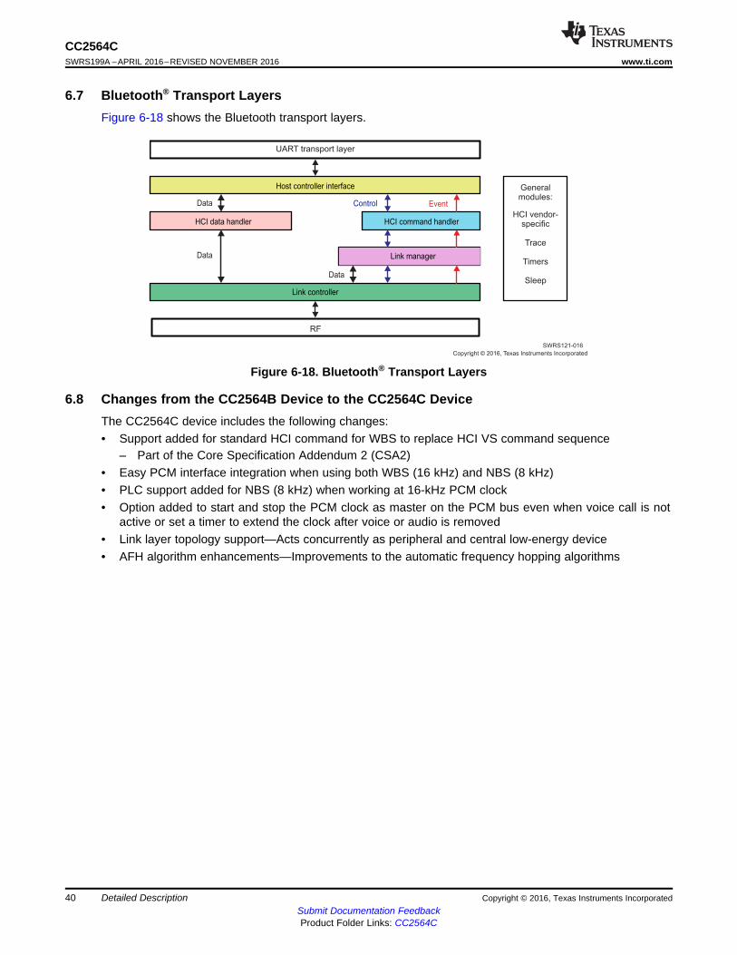
6.7 Bluetooth® Transport LayersFigure 6-18 shows the Bluetooth transport layers.
Figure 6-18. Bluetooth® Transport Layers
6.8 Changes from the CC2564B Device to the CC2564C DeviceThe CC2564C device includes the following changes:• Support added for standard HCI command for WBS to replace HCI VS command sequence
– Part of the Core Specification Addendum 2 (CSA2)• Easy PCM interface integration when using both WBS (16 kHz) and NBS (8 kHz)• PLC support added for NBS (8 kHz) when working at 16-kHz PCM clock• Option added to start and stop the PCM clock as master on the PCM bus even when voice call is not
active or set a timer to extend the clock after voice or audio is removed• Link layer topology support—Acts concurrently as peripheral and central low-energy device• AFH algorithm enhancements—Improvements to the automatic frequency hopping algorithms

41
CC2564Cwww.ti.com SWRS199A –APRIL 2016–REVISED NOVEMBER 2016
Submit Documentation FeedbackProduct Folder Links: CC2564C
Applications, Implementation, and LayoutCopyright © 2016, Texas Instruments Incorporated
7 Applications, Implementation, and Layout
NOTEInformation in the following Applications section is not part of the TI component specification,and TI does not warrant its accuracy or completeness. TI’s customers are responsible fordetermining suitability of components for their purposes. Customers should validate and testtheir design implementation to confirm system functionality.
7.1 Reference Design Schematics and BOM for Power and Radio Connections
Figure 7-1 shows the reference schematics for the VQFN-MR package. For complete schematics andPCB layout guidelines, contact your TI representative.

NC
CC256XRVM
Copyright © 2016, Texas Instruments IncorporatedApplications, Implementation, and LayoutSubmit Documentation FeedbackProduct Folder Links: CC2564C
42
CC2564CSWRS199A –APRIL 2016–REVISED NOVEMBER 2016 www.ti.com
Figure 7-1. Reference Schematics

43
CC2564Cwww.ti.com SWRS199A –APRIL 2016–REVISED NOVEMBER 2016
Submit Documentation FeedbackProduct Folder Links: CC2564C
Applications, Implementation, and LayoutCopyright © 2016, Texas Instruments Incorporated
Table 7-1 lists the BOM for the VQFN-MR package.
Table 7-1. Bill of Materials
QTY REF.DES. VALUE DESCRIPTION MANUFACTURER MANUFACTURER
PART NUMBERALT
PART NOTES
1 ANT1 NA ANT_IIFA_CC2420_32mil_MIR NA IIFA_CC2420 Chipantenna
Copper antennaon PCB
6 Capacitor 0.1 µF Capacitor, ceramic; 0.1-µF6.3-V 10% X7R 0402 Kemet C0402C104K9RACTU
2 Capacitor 1.0 µF Capacitor, ceramic; 1.0-µF6.3-V 10% X5R 0402 Taiyo Yuden JMK105BJ105KV-F
2 Capacitor 12 pF Capacitor, ceramic; 12 pF6.3-V X5R 10% 0402 Murata Electronics GRM1555C1H120JZ01D
2 Capacitor 0.47 µF Capacitor, ceramic; 0.47-µF6.3-V X5R ±10% 0402 Taiyo Yuden JMK105BJ474KV-F
1 FL1 2.45 GHz Filter, ceramic bandpass,2.45-GHz SMD Murata Electronics LFB212G45SG8C341
DEA162450BT_1260B3(TDK)
Place brownmarking up
1 OSC1 32.768 kHz 15 pF Oscillator; 32.768-kHz 15-pF1.5-V 3.3-V SMD
AbraconCorporation ASH7K-32.768KHZ-T Optional
1 U5 CC2564CRVM CC2564C dual-mode Bluetoothcontroller Texas Instruments CC2564CRVM
1 Y1 26 MHz Crystal, 26 MHz NDK NX2016SATZ1325D(Tai-SawTST)
1 C31 22 pF Capacitor, ceramic; 22-pF25-V 5% NP0 0201
Murata ElectronicsNorth America
GRM0335C1E220JD01D(EXS00A-CS06025)
7.2 PCB Layout GuidelinesThis section describes the PCB guidelines to speed up the PCB design using the CC256x QFN device.Following these guidelines ensures that the design will pass Bluetooth SIG certification and also minimizesrisk for regulatory certifications including FCC, ETSI, and CE. For more information, see CC256x QFNPCB Guidelines.
7.2.1 General PCB GuidelinesGeneral PCB guidelines follow:• You must verify the recommended PCB stackup in the PCB Design guidelines.• You must verify the dimensions of the QFN PCB footprint in the QFN Package Information section of
CC256x QFN PCB Guidelines and in Section 6.• The decoupling capacitors must be as close as possible to the QFN device.

44
CC2564CSWRS199A –APRIL 2016–REVISED NOVEMBER 2016 www.ti.com
Submit Documentation FeedbackProduct Folder Links: CC2564C
Applications, Implementation, and Layout Copyright © 2016, Texas Instruments Incorporated
7.2.2 Power Supply GuidelinesGuidelines for the power supply follow:• The trace width must be at least 10 mils for the VBAT and VIO traces.• The length of the traces must be as short as possible (pin to pin).• Decoupling capacitors must be as close as possible to the QFN device:
– The MLDO_IN capacitor must be close to pin B5.– The VDD_IO capacitor must be close to pins B18 and A17.
Guidelines for the LDOs follow:• The trace width for the trace between x_LDO_x pins and decoupling capacitors is at least 5 mils;
where possible, the recommended trace width is 10 mils.• Place the decoupling capacitor of MLDO_OUT (C20) as close as possible to pin A5.• These capacitors must close to the following pins:
– The DIG_LDO_OUT capacitor must be close to ball B15.– The DIG_LDO_OUT capacitor must be close to ball B27.– The DIG_LDO_OUT capacitor must be close to ball B36.
• The DIG_LDO_OUT capacitor connected to ball B36 must be isolated from the top layer GND (see theLow-Dropout Capacitors section in CC256x QFN PCB Guidelines).
• The decoupling capacitors for SRAM, ADCPPA, and CL1.5 LDO_OUT must be as close as possible totheir corresponding pins on the CC256x device.
• Place the device and capacitors together on the top side.• The ground connection of each capacitor must be directly connected to solid ground layer (layer 2).• The capacitor that is directly connected to pin A12 should be close to the device.• Connect the DCO_LDO_OUT capacitor isolated from layer 1 ground directly to layer 2 solid ground.
Guidelines for the ground layer follow:• Layer 2 must be a solid ground plane.• Isolate VSS_FREF from ground on the top layer and route it directly to ground on the second layer
(see the Key VSS Ball section in CC256x QFN PCB Guidelines).• Isolate VSS_DCO (ball B11) from ground. Include VSS_DCO in the illustration of the DCO_LDO_OUT
capacitor (see the DCO_LDO_OUT section in CC256x QFN PCB Guidelines).• A minimum of 13 vias on the thermal pad are required to increase ground coupling.• Connect VSS_FREF (ball B3) directly to solid ground, not to the thermal pad.

45
CC2564Cwww.ti.com SWRS199A –APRIL 2016–REVISED NOVEMBER 2016
Submit Documentation FeedbackProduct Folder Links: CC2564C
Applications, Implementation, and LayoutCopyright © 2016, Texas Instruments Incorporated
7.2.3 User InterfacesGuidelines for the UART follow:• The trace width for the UART must be at least 5 mils.• Run the four UART lines as a bus interface.• Determine if clocks, DC supply, or RF traces are not near these UART traces.• The ground plane on layer 2 is solid below these lines and there is ground around these traces on the
top layer.
Guidelines for the PCM follow:• The trace width for the PCM must be at least 5 mils.• Run the four PCM lines as a bus interface and approximately the same length.• Determine if clocks, DC supply, RF traces, and LDO capacitors are not near these PCM traces.• The ground plane on layer 2 is solid below these lines and there is ground around these traces on the
top layer.• Guidelines for TX_DBG follow:• Check for an accessible test point on the board from TX_DBG pin B24.
7.2.4 Clock InterfacesGuidelines for the slow clock follow:• The trace width for the slow clock must be at least 5 mils.• The signal lines for the slow clock must be as short as possible.• The ground plane on layer 2 is solid below these lines and there is ground around these traces on the
top layer.
Guidelines for the fast clock follow:• The trace width for the fast clock must be at least 5 mils.• Ensure that crystal tuning capacitors are close to crystal pads.• Make both traces (XTALM and XTALP) parallel as much as possible and approximately the same
length.• The ground plane on layer 2 is solid below these lines and there is ground around these traces on the
top layer.

46
CC2564CSWRS199A –APRIL 2016–REVISED NOVEMBER 2016 www.ti.com
Submit Documentation FeedbackProduct Folder Links: CC2564C
Applications, Implementation, and Layout Copyright © 2016, Texas Instruments Incorporated
7.2.5 RF InterfaceGuidelines for the RF Interface follow:• TI recommends using an RF shield (not mandatory).• Verify that RF traces are routed on the top layer and matched at 50 Ω with reference to ground.• Route the RF line between these NC pins:
– NC_2 (A10)– NC_3 (A11)– NC_14 (B9)– NC_15 (B10)These NC pins are grounded for better RF isolation.
NOTEThese pins are NC at the chip level, but TI recommends grounding them on the PCB layoutfor better RF isolation.
• Ensure the area underneath the BPF pads is grounded on layer 1 and layer 2.• Keep RF_IN and RF_OUT of the BPF pads clear of any ground fill (see the RF Trace section in
CC256x QFN PCB Guidelines).• Follow guidelines specified in the vendor-specific antenna design guides (including placement of
antenna).• Follow guidelines specified in the vendor-specific BPF design guides.• Verify that the Bluetooth RF trace is a 50-Ω, impedance-controlled trace with reference to solid ground.• Ensure that the RF trace length is as short as possible.

CC2564C
ZLLL G3YM7
= Last digit of the year= Month in hex number, 1-C for Jan-Dec= Primary site code for ANM= Secondary site code for ANM= Assembly lot code= Pin 1 indicator
YM7ZLLL
CC2564C xxx x
PrefixX = Experimental deviceBlank = Qualified device
Generic Part NumberPackage Designator
RVM = VQFNP-MR YFV = DSBGA
R = Large ReelT = Small Reel
Copyright © 2016, Texas Instruments Incorporated
47
CC2564Cwww.ti.com SWRS199A –APRIL 2016–REVISED NOVEMBER 2016
Submit Documentation FeedbackProduct Folder Links: CC2564C
Device and Documentation SupportCopyright © 2016, Texas Instruments Incorporated
8 Device and Documentation Support
8.1 Third-Party Products DisclaimerTI'S PUBLICATION OF INFORMATION REGARDING THIRD-PARTY PRODUCTS OR SERVICES DOESNOT CONSTITUTE AN ENDORSEMENT REGARDING THE SUITABILITY OF SUCH PRODUCTS ORSERVICES OR A WARRANTY, REPRESENTATION OR ENDORSEMENT OF SUCH PRODUCTS ORSERVICES, EITHER ALONE OR IN COMBINATION WITH ANY TI PRODUCT OR SERVICE.
8.2 Tools and SoftwareDesign Kits and Evaluation ModulesCC256x Bluetooth® Hardware Evaluation Tool This intuitive, user-friendly TI tool is used to evaluate
TI's Bluetooth chips and can be downloaded as a complete package from the TI web site.More specifically, the tool is used to configure the properties of the Bluetooth chip throughthe Service Pack (SP) and also allows testing of RF performance.
For a complete listing of development-support tools, see the TI CC256x wiki. For information on pricingand availability, contact the nearest TI field sales office or authorized distributor.
8.3 Device NomenclatureTo designate the stages in the product development cycle, TI assigns prefixes to the part numbers. Theseprefixes represent evolutionary stages of product development from engineering prototypes through fullyqualified production devices.
Device development evolutionary flow:X Experimental device that is not necessarily representative of the final device's electrical
specifications and may not use production assembly flow.P Prototype device that is not necessarily the final silicon die and may not necessarily meet
final electrical specifications.null Production version of the silicon die that is fully qualified.
Figure 8-1. CC2564C Device Nomenclature Figure 8-2. Chip Markings (VQFN-MR Package)
48
CC2564CSWRS199A –APRIL 2016–REVISED NOVEMBER 2016 www.ti.com
Submit Documentation FeedbackProduct Folder Links: CC2564C
Device and Documentation Support Copyright © 2016, Texas Instruments Incorporated
8.4 Documentation SupportTo receive notification of documentation updates, navigate to the device product folder on ti.com. In theupper right corner, click on Alert me to register and receive a weekly digest of any product information thathas changed. For change details, review the revision history included in any revised document.
The current documentation that describes the DSP, related peripherals, and other technical collateral is asfollows:
Application ReportsCC2564C Bluetooth 4.1 and 4.2 Application NotesCC256x QFN PCB Guidelines
User's GuidesCC2564B to CC2564C Migration GuideCC256xC QFN EM User’s GuideCC256x Reference Design FilesCC2564 Audio Sink Reference DesignCC256x Hardware Design Checklist
8.5 Community ResourcesThe following links connect to TI community resources. Linked contents are provided "AS IS" by therespective contributors. They do not constitute TI specifications and do not necessarily reflect TI's views;see TI's Terms of Use.TI E2E™ Online Community The TI engineer-ro-engineer (E2E) community was created to foster
collaboration among engineers. At e2e.ti.com, you can ask questions, share knowledge,explore ideas and help solve problems with fellow engineers.
TI Embedded Processors Wiki Established to help developers get started with Embedded Processorsfrom Texas Instruments and to foster innovation and growth of general knowledge about thehardware and software surrounding these devices.
8.6 TrademarksE2E is a trademark of Texas Instruments.ARM7TDMI is a registered trademark of ARM Limited.iPod is a registered trademark of Apple, Inc.Bluetooth is a registered trademark of Bluetooth SIG, Inc.All other trademarks are the property of their respective owners.
8.7 Electrostatic Discharge CautionThis integrated circuit can be damaged by ESD. Texas Instruments recommends that all integrated circuits be handled withappropriate precautions. Failure to observe proper handling and installation procedures can cause damage.
ESD damage can range from subtle performance degradation to complete device failure. Precision integrated circuits may be moresusceptible to damage because very small parametric changes could cause the device not to meet its published specifications.
8.8 GlossaryTI Glossary This glossary lists and explains terms, acronyms, and definitions.

49
CC2564Cwww.ti.com SWRS199A –APRIL 2016–REVISED NOVEMBER 2016
Submit Documentation FeedbackProduct Folder Links: CC2564C
Mechanical, Packaging, and Orderable InformationCopyright © 2016, Texas Instruments Incorporated
9 Mechanical, Packaging, and Orderable Information
The following pages include mechanical, packaging, and orderable information. This information is themost current data available for the designated devices. This data is subject to change without notice andrevision of this document. For browser-based versions of this data sheet, refer to the left-hand navigation.

PACKAGE OPTION ADDENDUM
www.ti.com 18-Nov-2016
Addendum-Page 1
PACKAGING INFORMATION
Orderable Device Status(1)
Package Type PackageDrawing
Pins PackageQty
Eco Plan(2)
Lead/Ball Finish(6)
MSL Peak Temp(3)
Op Temp (°C) Device Marking(4/5)
Samples
CC2564CRVMR ACTIVE VQFNP-MR RVM 76 2500 Green (RoHS& no Sb/Br)
CU SN Level-3-260C-168 HR -40 to 85 CC2564C
CC2564CRVMT ACTIVE VQFNP-MR RVM 76 250 Green (RoHS& no Sb/Br)
CU SN Level-3-260C-168 HR -40 to 85 CC2564C
(1) The marketing status values are defined as follows:ACTIVE: Product device recommended for new designs.LIFEBUY: TI has announced that the device will be discontinued, and a lifetime-buy period is in effect.NRND: Not recommended for new designs. Device is in production to support existing customers, but TI does not recommend using this part in a new design.PREVIEW: Device has been announced but is not in production. Samples may or may not be available.OBSOLETE: TI has discontinued the production of the device.
(2) Eco Plan - The planned eco-friendly classification: Pb-Free (RoHS), Pb-Free (RoHS Exempt), or Green (RoHS & no Sb/Br) - please check http://www.ti.com/productcontent for the latest availabilityinformation and additional product content details.TBD: The Pb-Free/Green conversion plan has not been defined.Pb-Free (RoHS): TI's terms "Lead-Free" or "Pb-Free" mean semiconductor products that are compatible with the current RoHS requirements for all 6 substances, including the requirement thatlead not exceed 0.1% by weight in homogeneous materials. Where designed to be soldered at high temperatures, TI Pb-Free products are suitable for use in specified lead-free processes.Pb-Free (RoHS Exempt): This component has a RoHS exemption for either 1) lead-based flip-chip solder bumps used between the die and package, or 2) lead-based die adhesive used betweenthe die and leadframe. The component is otherwise considered Pb-Free (RoHS compatible) as defined above.Green (RoHS & no Sb/Br): TI defines "Green" to mean Pb-Free (RoHS compatible), and free of Bromine (Br) and Antimony (Sb) based flame retardants (Br or Sb do not exceed 0.1% by weightin homogeneous material)
(3) MSL, Peak Temp. - The Moisture Sensitivity Level rating according to the JEDEC industry standard classifications, and peak solder temperature.
(4) There may be additional marking, which relates to the logo, the lot trace code information, or the environmental category on the device.
(5) Multiple Device Markings will be inside parentheses. Only one Device Marking contained in parentheses and separated by a "~" will appear on a device. If a line is indented then it is a continuationof the previous line and the two combined represent the entire Device Marking for that device.
(6) Lead/Ball Finish - Orderable Devices may have multiple material finish options. Finish options are separated by a vertical ruled line. Lead/Ball Finish values may wrap to two lines if the finishvalue exceeds the maximum column width.
Important Information and Disclaimer:The information provided on this page represents TI's knowledge and belief as of the date that it is provided. TI bases its knowledge and belief on informationprovided by third parties, and makes no representation or warranty as to the accuracy of such information. Efforts are underway to better integrate information from third parties. TI has taken andcontinues to take reasonable steps to provide representative and accurate information but may not have conducted destructive testing or chemical analysis on incoming materials and chemicals.TI and TI suppliers consider certain information to be proprietary, and thus CAS numbers and other limited information may not be available for release.

PACKAGE OPTION ADDENDUM
www.ti.com 18-Nov-2016
Addendum-Page 2
In no event shall TI's liability arising out of such information exceed the total purchase price of the TI part(s) at issue in this document sold by TI to Customer on an annual basis.

TAPE AND REEL INFORMATION
*All dimensions are nominal
Device PackageType
PackageDrawing
Pins SPQ ReelDiameter
(mm)
ReelWidth
W1 (mm)
A0(mm)
B0(mm)
K0(mm)
P1(mm)
W(mm)
Pin1Quadrant
CC2564CRVMT VQFNP-MR
RVM 76 250 180.0 16.4 8.35 8.35 1.7 12.0 16.0 Q2
PACKAGE MATERIALS INFORMATION
www.ti.com 21-Nov-2016
Pack Materials-Page 1

*All dimensions are nominal
Device Package Type Package Drawing Pins SPQ Length (mm) Width (mm) Height (mm)
CC2564CRVMT VQFNP-MR RVM 76 250 213.0 191.0 55.0
PACKAGE MATERIALS INFORMATION
www.ti.com 21-Nov-2016
Pack Materials-Page 2


IMPORTANT NOTICE
Texas Instruments Incorporated and its subsidiaries (TI) reserve the right to make corrections, enhancements, improvements and otherchanges to its semiconductor products and services per JESD46, latest issue, and to discontinue any product or service per JESD48, latestissue. Buyers should obtain the latest relevant information before placing orders and should verify that such information is current andcomplete. All semiconductor products (also referred to herein as “components”) are sold subject to TI’s terms and conditions of salesupplied at the time of order acknowledgment.TI warrants performance of its components to the specifications applicable at the time of sale, in accordance with the warranty in TI’s termsand conditions of sale of semiconductor products. Testing and other quality control techniques are used to the extent TI deems necessaryto support this warranty. Except where mandated by applicable law, testing of all parameters of each component is not necessarilyperformed.TI assumes no liability for applications assistance or the design of Buyers’ products. Buyers are responsible for their products andapplications using TI components. To minimize the risks associated with Buyers’ products and applications, Buyers should provideadequate design and operating safeguards.TI does not warrant or represent that any license, either express or implied, is granted under any patent right, copyright, mask work right, orother intellectual property right relating to any combination, machine, or process in which TI components or services are used. Informationpublished by TI regarding third-party products or services does not constitute a license to use such products or services or a warranty orendorsement thereof. Use of such information may require a license from a third party under the patents or other intellectual property of thethird party, or a license from TI under the patents or other intellectual property of TI.Reproduction of significant portions of TI information in TI data books or data sheets is permissible only if reproduction is without alterationand is accompanied by all associated warranties, conditions, limitations, and notices. TI is not responsible or liable for such altereddocumentation. Information of third parties may be subject to additional restrictions.Resale of TI components or services with statements different from or beyond the parameters stated by TI for that component or servicevoids all express and any implied warranties for the associated TI component or service and is an unfair and deceptive business practice.TI is not responsible or liable for any such statements.Buyer acknowledges and agrees that it is solely responsible for compliance with all legal, regulatory and safety-related requirementsconcerning its products, and any use of TI components in its applications, notwithstanding any applications-related information or supportthat may be provided by TI. Buyer represents and agrees that it has all the necessary expertise to create and implement safeguards whichanticipate dangerous consequences of failures, monitor failures and their consequences, lessen the likelihood of failures that might causeharm and take appropriate remedial actions. Buyer will fully indemnify TI and its representatives against any damages arising out of the useof any TI components in safety-critical applications.In some cases, TI components may be promoted specifically to facilitate safety-related applications. With such components, TI’s goal is tohelp enable customers to design and create their own end-product solutions that meet applicable functional safety standards andrequirements. Nonetheless, such components are subject to these terms.No TI components are authorized for use in FDA Class III (or similar life-critical medical equipment) unless authorized officers of the partieshave executed a special agreement specifically governing such use.Only those TI components which TI has specifically designated as military grade or “enhanced plastic” are designed and intended for use inmilitary/aerospace applications or environments. Buyer acknowledges and agrees that any military or aerospace use of TI componentswhich have not been so designated is solely at the Buyer's risk, and that Buyer is solely responsible for compliance with all legal andregulatory requirements in connection with such use.TI has specifically designated certain components as meeting ISO/TS16949 requirements, mainly for automotive use. In any case of use ofnon-designated products, TI will not be responsible for any failure to meet ISO/TS16949.
Products ApplicationsAudio www.ti.com/audio Automotive and Transportation www.ti.com/automotiveAmplifiers amplifier.ti.com Communications and Telecom www.ti.com/communicationsData Converters dataconverter.ti.com Computers and Peripherals www.ti.com/computersDLP® Products www.dlp.com Consumer Electronics www.ti.com/consumer-appsDSP dsp.ti.com Energy and Lighting www.ti.com/energyClocks and Timers www.ti.com/clocks Industrial www.ti.com/industrialInterface interface.ti.com Medical www.ti.com/medicalLogic logic.ti.com Security www.ti.com/securityPower Mgmt power.ti.com Space, Avionics and Defense www.ti.com/space-avionics-defenseMicrocontrollers microcontroller.ti.com Video and Imaging www.ti.com/videoRFID www.ti-rfid.comOMAP Applications Processors www.ti.com/omap TI E2E Community e2e.ti.comWireless Connectivity www.ti.com/wirelessconnectivity
Mailing Address: Texas Instruments, Post Office Box 655303, Dallas, Texas 75265Copyright © 2016, Texas Instruments Incorporated