cc3000 ieee 802.11b/g solution module · cc3000 swrs126 –november 2012 table 1. cc3000 module...
TRANSCRIPT

SWRS126-013
Product
Folder
Sample &Buy
Technical
Documents
Tools &
Software
Support &Community
CC3000
www.ti.com SWRS126 –NOVEMBER 2012
TI SimpleLink™ CC3000 Module – Wi-Fi 802.11b/g Network Processor1FEATURES • Operating temperature: –20°C to 70°C
• Based on TI's seventh generation of proven234• Wireless network processor
Wi-Fi solutions– IEEE 802.11 b/g• Complete platform solution including user and– Embedded IPv4 TCP/IP stack
porting guides, API guide, sample• Best-in-class radio performance Wi-Fi™ applications, and support community
– TX power: +18.0 dBm at 11 Mbps, CCK– RX sensitivity: –88 dBm, 8% PER, 11 Mbps APPLICATIONS
• Works with low MIPS and low-cost MCUs with • Home automationcompact memory footprint • Home security
• FCC, IC, and CE certified with a chip antenna • Connected appliances• HW design files and design guide available • Smart energy
from TI• M2M communication
• Integrated crystal and power management• Small form factor: 16.3 mm × 13.5 mm × 2 mm
DESCRIPTIONThe TI CC3000 module is a self-contained wireless network processor that simplifies the implementation ofInternet connectivity (see Figure 1). TI's SimpleLink™ Wi-Fi solution minimizes the software requirements of thehost microcontroller (MCU) and is thus the ideal solution for embedded applications using any low-cost and low-power MCU.
The TI CC3000 module reduces development time, lowers manufacturing costs, saves board space, easescertification, and minimizes the RF expertise required. This complete platform solution includes software drivers,sample applications, API guide, user documentation, and a world-class support community.
For more information on TI’s wireless platform solutions for Wi-Fi, go to TI's Wireless Connectivity wiki(www.ti.com/connectivitywiki).
Figure 1. Wi-Fi Solution for TI SimpleLink CC3000 Module
1
Please be aware that an important notice concerning availability, standard warranty, and use in critical applications ofTexas Instruments semiconductor products and disclaimers thereto appears at the end of this data sheet.
2SimpleLink, Smart Config are trademarks of Texas Instruments.3Wi-Fi is a trademark of Wi-Fi Alliance.4All other trademarks are the property of their respective owners.
PRODUCTION DATA information is current as of publication date. Copyright © 2012, Texas Instruments IncorporatedProducts conform to specifications per the terms of the TexasInstruments standard warranty. Production processing does notnecessarily include testing of all parameters.
Not Recommended For New Designs

CC3000
SWRS126 –NOVEMBER 2012 www.ti.com
This integrated circuit can be damaged by ESD. Texas Instruments recommends that all integrated circuits be handled withappropriate precautions. Failure to observe proper handling and installation procedures can cause damage.
ESD damage can range from subtle performance degradation to complete device failure. Precision integrated circuits may be moresusceptible to damage because very small parametric changes could cause the device not to meet its published specifications.
FEATURES
WLAN• 802.11b/g integrated radio, modem, and MAC supporting WLAN communication as a BSS station with CCK
and OFDM rates from 1 to 54 Mbps in the 2.4-GHz ISM band• Auto-calibrated radio with a single-ended 50-Ω interface enables easy connection to the antenna without
requiring expertise in radio circuit design.• Advanced connection manager with seven user-configurable profiles stored in an NVMEM allows automatic
fast connection to an access point without user or host intervention.• Supports all Wi-Fi security modes for personal networks: WEP, WPA, and WPA2 with on-chip security
accelerators• Smart Config™ WLAN provisioning tools allow customers to connect a headless device to a WLAN network
using a smart phone, tablet, or PC.
Network Stack• Integrated IPv4 TCP/IP stack with BSD socket APIs enables simple internet connectivity with any
microcontroller, microprocessor, or ASIC.• Supports four simultaneous TCP or UDP sockets• Built-in network protocols: ARP, ICMP, DHCP client, and DNS client enable easy connection to the local
network and to the Internet.
Host Interface and Driver• Interfaces over 4-wire serial peripheral interface (SPI) with any microcontroller, or processor at clock speed
up to16 MHz• Low footprint driver provided for TI MCUs and easily ported to any processor or ASIC• Simple APIs enable easy integration with any single-threaded or multi-threaded application.
System• Works from a single, preregulated power supply or connects directly to a battery• Separated I/O voltage rail allows flexible integration with host processors• Ultra-low leakage shut-down mode with current <5 µA• Integrated clock sources
EEPROM• Integrated EEPROM stores firmware patch, network configuration, and MAC address.• Programmable through an I2C interface or over APIs from the host, allowing over-the-air firmware upgrades• Can store 5 KB of user data accessible to the host application, enhancing the MCU NVM
2 Submit Documentation Feedback Copyright © 2012, Texas Instruments Incorporated
Product Folder Links: CC3000
Not Recommended For New Designs

13.5000
16.3000
0.5000 0.7000
1.2000
0.3000
1.9000
1.9000
2.1000
1.7000
1.9000
2.4000
1.9000 2.1000
1.2000
1.20000.7000
1.9000
Unit: mm
36 29
4643
29
28
4037
38 41
4239
19
4544
1811
10
PIN-1
SWRS126-002
CC3000
www.ti.com SWRS126 –NOVEMBER 2012
PACKAGE INFORMATION
Module Outline
For the PCB layout of your applications, TI recommends the footprint shown in Figure 2.
Figure 2. CC3000 Module Footprint and Pinouts
Pin Description
Table 1 describes the CC3000 module pins.
Table 1. CC3000 Module Pins Description
Pin Signal Name Type State at State After Voltage Level DescriptionReset Reset
1 GND GND — — — Ground
2 Reserved_1 — — — 1.8 V Reserved. Connect to test point.
3 NC — — — — Not connected
4 Reserved_2 — — — 1.8 V Reserved. Connect to test point.
5 WL_EN2 (1) I Hi-Z — — Mode setting
6 WL_RS232_TX (2) O Hi-Z Force 1 1.8 V RS232 test-mode signal (1.8-V logic).Connect to test point. Serial connectionfor CC3000 radio tool.
7 WL_EN1 I Hi-Z — — Mode setting
8 WL_RS232_RX (2) I Hi-Z PU 1.8 V RS232 test-mode signal (1.8-V logic).Connect to test point. Serial connectionfor CC3000 radio tool.
9 GND GND — — — Ground
10 GND GND — — — Ground
11 GND GND — — — Ground
12 SPI_CS I Hi-Z PU VIO_HOST Host interface SPI chip-select (CS)
13 SPI_DOUT O Hi-Z PU VIO_HOST Host interface SPI data out
14 SPI_IRQ O Hi-Z Force 1 VIO_HOST Host interface SPI interrupt
(1) Connect WL_EN1 to WL_EL2 for proper operation of the module.(2) Leave unconnected in function module.
Copyright © 2012, Texas Instruments Incorporated Submit Documentation Feedback 3
Product Folder Links: CC3000
Not Recommended For New Designs

CC3000
SWRS126 –NOVEMBER 2012 www.ti.com
Table 1. CC3000 Module Pins Description (continued)
Pin Signal Name Type State at State After Voltage Level DescriptionReset Reset
15 SPI_DIN I Hi-Z PU VIO_HOST Host interface SPI data in
16 GND GND — — — Ground
17 SPI_CLK I Hi-Z PD VIO_HOST Host interface SPI clock
18 GND GND — — — Ground
19 VBAT_IN Power — — VBAT Power supply input, 2.7 to 4.8 V
20 GND GND — — — Ground
21 EXT_32K — — — — Not used. Connect to ground.
22 GND GND — — — Ground
23 VIO_HOST Power — — VIO_HOST VIO host supply voltage
24 Reserved 3 — — — — Reserved. Connect to test point.
25 GND GND — — — Ground
26 VBAT_SW_EN I — — VIO_HOST Module enable. Connect to host GPIO.
27 SDA_EEPROM (3) I/O 1.8 V I2C data line from EEPROM
28 SDA_CC3000 (3) I/O 1.8 V I2C data line from the CC3000 module
29 SCL_EEPROM (4) I/O 1.8 V I2C clock line from EEPROM
30 SCL_CC3000 (4) I/O 1.8 V I2C clock line from the CC3000module
31 GND GND — — — Ground
32 GND GND — — — Ground
33 GND GND — — — Ground
34 GND GND — — — Ground
35 RF_ANT RF — — — WLAN antenna port, 50-Ω single
36 GND GND — — — Ground
37 GND GND — — — Ground
38 GND GND — — — Ground
39 GND GND — — — Ground
40 GND GND — — — Ground
41 GND GND — — — Ground
42 GND GND — — — Ground
43 GND GND — — — Ground
44 GND GND — — — Ground
45 GND GND — — — Ground
46 GND GND — — — Ground
(3) Connect SDA_EEPROM and SDA_CC3000 through a 0-Ω resistor.(4) Connect SLC_EEPROM and SLC_CC3000 through a 0-Ω resistor.
4 Submit Documentation Feedback Copyright © 2012, Texas Instruments Incorporated
Product Folder Links: CC3000
Not Recommended For New Designs
CC3000
www.ti.com SWRS126 –NOVEMBER 2012
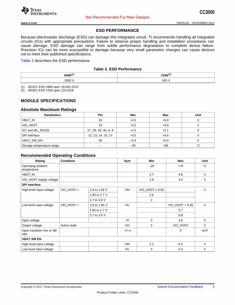
ESD PERFORMANCE
Because electrostatic discharge (ESD) can damage this integrated circuit, TI recommends handling all integratedcircuits (ICs) with appropriate precautions. Failure to observe proper handling and installation procedures cancause damage. ESD damage can range from subtle performance degradation to complete device failure.Precision ICs can be more susceptible to damage because very small parametric changes can cause devicesnot to meet their published specifications.
Table 2 describes the ESD performance.
Table 2. ESD Performance
HDM (1) CDM (2)
1000 V 500 V
(1) JEDEC ESD HBM spec JS-001-2012(2) JEDEC ESD CDM spec 22C101E
spaceMODULE SPECIFICATIONS
Absolute Maximum RatingsParameters Pin Min Max Unit
VBAT_IN 19 –0.5 +6.0 V
VIO_HOST 23 –0.5 +4.6 V
I2C and WL_RS232 27, 28, 29, 30, 6, 8 –0.5 +2.1 V
SPI interface 12, 13, 14, 15, 17 –0.5 +4.6 V
VBAT_SW_EN 26 –0.3 +6.0 V
Storage temperature range – –40 +85 °C
Recommended Operating ConditionsRating Condition Sym Min Max Unit
Operating ambient –20 +70 °Ctemperature
VBAT_IN 2.7 4.8 V
VIO_HOST supply voltage 1.8 3.6 V
SPI interface
High-level input voltage VIO_HOST = 1.8 to 1.95 V VIH VIO_HOST x 0.65 V
1.95 to 2.7 V 1.6
2.7 to 3.6 V 2
Low-level input voltage VIO_HOST = 1.8 to 1.95 V VIL VIO_HOST × 0.35 V
1.95 to 2.7 V 0.7
2.7 to 3.6 V 0.8
Input voltage VI 0 3.6 V
Output voltage Active state VO 0 VIO_HOST V
Input transition rise or fall △t/△v 5 ns/Vrate
VBAT SW EN
High-level input voltage VIH 1.1 5.5 V
Low-level input voltage VIL 0 0.4 V
Copyright © 2012, Texas Instruments Incorporated Submit Documentation Feedback 5
Product Folder Links: CC3000
Not Recommended For New Designs
CC3000
SWRS126 –NOVEMBER 2012 www.ti.com
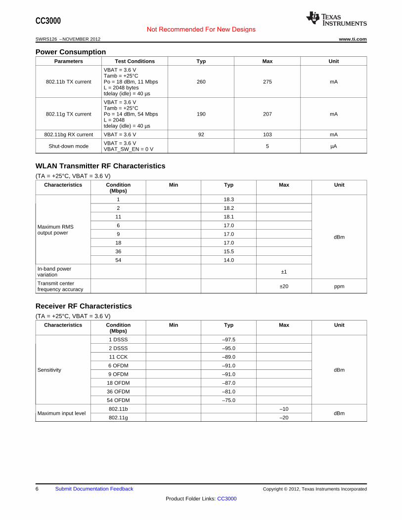
Power ConsumptionParameters Test Conditions Typ Max Unit
VBAT = 3.6 VTamb = +25°C
802.11b TX current Po = 18 dBm, 11 Mbps 260 275 mAL = 2048 bytestdelay (idle) = 40 µs
VBAT = 3.6 VTamb = +25°C
802.11g TX current Po = 14 dBm, 54 Mbps 190 207 mAL = 2048tdelay (idle) = 40 µs
802.11bg RX current VBAT = 3.6 V 92 103 mA
VBAT = 3.6 VShut-down mode 5 µAVBAT_SW_EN = 0 V
WLAN Transmitter RF Characteristics(TA = +25°C, VBAT = 3.6 V)
Characteristics Condition Min Typ Max Unit(Mbps)
1 18.3
2 18.2
11 18.1
6 17.0Maximum RMSoutput power 9 17.0 dBm
18 17.0
36 15.5
54 14.0
In-band power ±1variation
Transmit center ±20 ppmfrequency accuracy
Receiver RF Characteristics(TA = +25°C, VBAT = 3.6 V)
Characteristics Condition Min Typ Max Unit(Mbps)
1 DSSS –97.5
2 DSSS –95.0
11 CCK –89.0
6 OFDM –91.0Sensitivity dBm
9 OFDM –91.0
18 OFDM –87.0
36 OFDM –81.0
54 OFDM –75.0
802.11b –10Maximum input level dBm
802.11g –20
6 Submit Documentation Feedback Copyright © 2012, Texas Instruments Incorporated
Product Folder Links: CC3000
Not Recommended For New Designs
SWRS126-004
Host captureCC3000 launchCC3000 captureHost launch
TclkTp
tintis
toh
tos
SPI_CLK(at device die)
SPI_DIN(data from host to device)
SPI_DOUT(data from host)device to
SWRS126-016
MCU SPI
master
CC3000
SPI slave
SPI_CLK
SPI_CS
SPI_IRQ
SPI_DOUT
SPI_DIN
CC3000
www.ti.com SWRS126 –NOVEMBER 2012
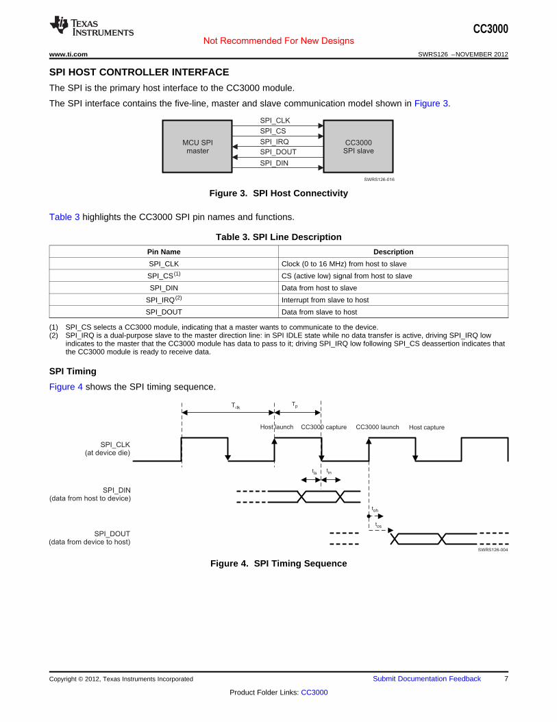
SPI HOST CONTROLLER INTERFACE
The SPI is the primary host interface to the CC3000 module.
The SPI interface contains the five-line, master and slave communication model shown in Figure 3.
Figure 3. SPI Host Connectivity
Table 3 highlights the CC3000 SPI pin names and functions.
Table 3. SPI Line Description
Pin Name Description
SPI_CLK Clock (0 to 16 MHz) from host to slave
SPI_CS (1) CS (active low) signal from host to slave
SPI_DIN Data from host to slave
SPI_IRQ (2) Interrupt from slave to host
SPI_DOUT Data from slave to host
(1) SPI_CS selects a CC3000 module, indicating that a master wants to communicate to the device.(2) SPI_IRQ is a dual-purpose slave to the master direction line: in SPI IDLE state while no data transfer is active, driving SPI_IRQ low
indicates to the master that the CC3000 module has data to pass to it; driving SPI_IRQ low following SPI_CS deassertion indicates thatthe CC3000 module is ready to receive data.
SPI Timing
Figure 4 shows the SPI timing sequence.
Figure 4. SPI Timing Sequence
Copyright © 2012, Texas Instruments Incorporated Submit Documentation Feedback 7
Product Folder Links: CC3000
Not Recommended For New Designs
CC3000
SWRS126 –NOVEMBER 2012 www.ti.com
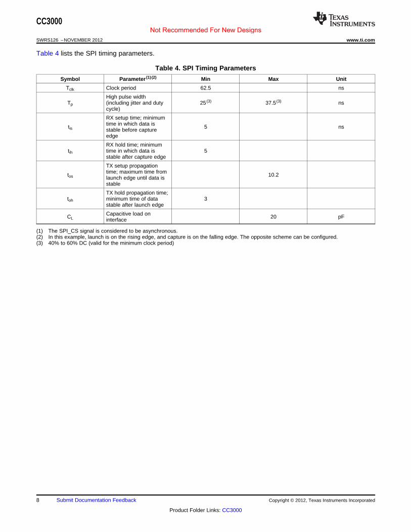
Table 4 lists the SPI timing parameters.
Table 4. SPI Timing Parameters
Symbol Parameter (1) (2) Min Max Unit
Tclk Clock period 62.5 ns
High pulse widthTp (including jitter and duty 25 (3) 37.5 (3) ns
cycle)
RX setup time; minimumtime in which data istis 5 nsstable before captureedge
RX hold time; minimumtih time in which data is 5
stable after capture edge
TX setup propagationtime; maximum time fromtos 10.2launch edge until data isstable
TX hold propagation time;toh minimum time of data 3
stable after launch edge
Capacitive load onCL 20 pFinterface
(1) The SPI_CS signal is considered to be asynchronous.(2) In this example, launch is on the rising edge, and capture is on the falling edge. The opposite scheme can be configured.(3) 40% to 60% DC (valid for the minimum clock period)
8 Submit Documentation Feedback Copyright © 2012, Texas Instruments Incorporated
Product Folder Links: CC3000
Not Recommended For New Designs
SWRS126-005
VBAT_IN
VIO_HOST
VBAT_SW_EN
SPI_IRQ
SPI_CST0 T1 T2
CC3000
www.ti.com SWRS126 –NOVEMBER 2012
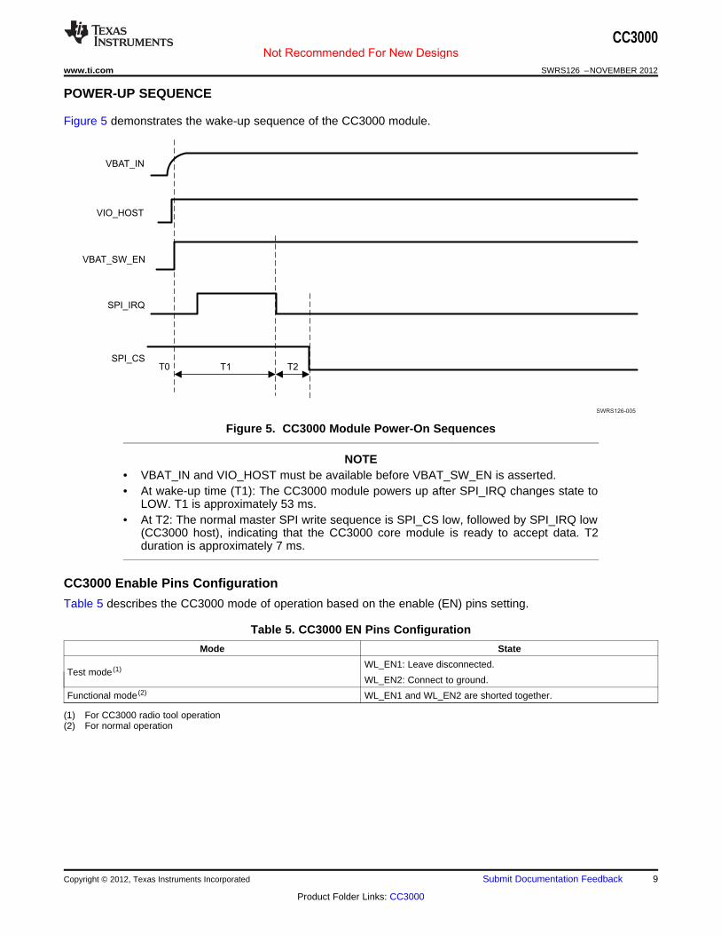
POWER-UP SEQUENCE
Figure 5 demonstrates the wake-up sequence of the CC3000 module.
Figure 5. CC3000 Module Power-On Sequences
NOTE• VBAT_IN and VIO_HOST must be available before VBAT_SW_EN is asserted.• At wake-up time (T1): The CC3000 module powers up after SPI_IRQ changes state to
LOW. T1 is approximately 53 ms.• At T2: The normal master SPI write sequence is SPI_CS low, followed by SPI_IRQ low
(CC3000 host), indicating that the CC3000 core module is ready to accept data. T2duration is approximately 7 ms.
CC3000 Enable Pins Configuration
Table 5 describes the CC3000 mode of operation based on the enable (EN) pins setting.
Table 5. CC3000 EN Pins Configuration
Mode State
WL_EN1: Leave disconnected.Test mode (1)
WL_EN2: Connect to ground.
Functional mode (2) WL_EN1 and WL_EN2 are shorted together.
(1) For CC3000 radio tool operation(2) For normal operation
Copyright © 2012, Texas Instruments Incorporated Submit Documentation Feedback 9
Product Folder Links: CC3000
Not Recommended For New Designs

TOP VIEW SIDE VIEW
CC3000MOD
Module Size: 16.3 x 13.5 x 2.0 mm
16.30 16.30
2.0013.50
SWRS126-007
PCUSB cable USB to serial
bridge1.8 V
CC3000
WL_RS232_TX
WL_RS232_RX
SWRS126-017
WL_EN2
CC3000
SWRS126 –NOVEMBER 2012 www.ti.com
Test Mode Serial Interface
The CC3000 module contains a dedicated WLAN serial interface to connect to the CC3000 radio tests tool, anexternal PC-based software test utility, during development and evaluation phase (see Figure 6 and Table 6).The CC3000 radio test tool utility can be obtained from the CC3000 TI wiki (www.ti.com/connectivitywiki).
Figure 6. CC3000 Test Mode Serial Interface Connection
Table 6. CC3000 Test Mode Debug Interface Description
Signal Name Function
WL_RS232_TXConnection with CC3000 radio PC-based software (1)
WL_RS232_RX
(1) WL_EN2 pins must be grounded while bringing up the CC3000 radio tool.
SURFACE MOUNT INFORMATION
The CC3000 module uses a flat shield cover designed for a fully automated assembly process. For baking andreflow recommendations, follow MSL level 4 found in the JEDEC/IPC Standard J-STD-20b. The classificationtemperature (TC) for the module is 250°C.
MECHANICAL INFORMATION
Module Mechanical Outline
Figure 7 shows the mechanical outline for the CC3000 module.
Figure 7. CC3000 Module Mechanical Outline
10 Submit Documentation Feedback Copyright © 2012, Texas Instruments Incorporated
Product Folder Links: CC3000
Not Recommended For New Designs

CC3000MOD
YYWWSSF
6.0 mm
SWRS126-008
CC3000
www.ti.com SWRS126 –NOVEMBER 2012
Package Marking
Figure 8 shows the CC3000 module package marking.
Figure 8. CC3000 Module Package Marking
Table 7 defines the marking code.
Table 7. Package Marking Definitions
Code Definition
YYWWSSF Date
YY Year (for example, 2012 = 12)
WW Week (01 through 53)
SS Serial number from 01 to 99 to match manufacturer lot number
F Reserved for internal use
Ordering Information
Table 8 lists the CC3000 module part numbers.
Table 8. CC3000 Module Part Numbers
Order Number Description
CC3000MOD CC3000 module, 44 modules per tray
CC3000MODR CC3000 module reel, 1200 modules per reel
Copyright © 2012, Texas Instruments Incorporated Submit Documentation Feedback 11
Product Folder Links: CC3000
Not Recommended For New Designs

TP4 and TP5 -CC3000 Radio Tool Connection 1.8V.
TI CC3000MOD Module Reference Design
Internal Power FET Switch Enable.Connect to Host GPIO.
VIO_HOST =Voltage level of the Host Interface.
VBAT_IN: 2.7V~4.8V => 3.6V TYP
The value of antenna matching componentsare match for CC3000MOD EM board
Connect to Host SPI Interface.
R4 R5Mode
Function mode
Test Modefor Radio Tool Operation
0R
0R
NC
NC
Optional for conductive measurment
WL_SPI_DOUT_HOST
WL_SPI_IRQ_HOST
WL_SPI_DIN_HOST
WL_SPI_CLK_HOST
WL_SPI_CS_HOST
VBAT_SW_EN
VBAT_IN
VIO_HOST
R4
NL
RES1005
L1
NL
IND1005
U1
CC3000MOD
4
2
7
5
3
6
8 21
25
9
30
29
28
27
22
14
13
12
17
15
26
19
35
31
33
16
34
23
32
37
38
39
40
41
42
43
44
46
45
1
18
10
20
24
11
36
RESERVED_2
RESERVED_1
WL_EN1
WL_EN2
NC
WL_RS232_TX
WL_RS232_RX EXT_32K
GND
GND
SC
L_
CC
300
0
SC
L_
EE
PR
OM
SDA_CC3000
SDA_EEPROM
GND
SP
I_IR
Q
SP
I_D
OU
T
SP
I_C
S
SP
I_C
LK
SP
I_D
IN
VBAT_SW_EN
VBAT_IN
RF
_A
NT
GN
D
GN
D
GN
D
GN
D
VIO_HOST
GN
D
GN
D
GN
D
GN
D
GN
D
GN
D
GN
D
GN
D
GN
D
GN
D
GN
D
GND
GN
D
GND
GND
RESERVED_3
GN
DG
ND
C5
1uF
CAP1005
TP5
L2
2.2nH
IND1005
TP3
C4
1uF
CAP1005
R5
0R
RES1005
C3 NL_10pF
CAP1005
TP2
R2
0R
RES1005
TP4
C1
2.2pF
CAP1005
ANT1
AT8010-E2R9HAA
8.0x1.0x1.0mm
1
2
C2
10pF
CAP1005
TP1
J1
NL_U.FL-R-SMT(10)
U.FL
1
2
3
R1
0R
RES1005
SWRS126-009
CC3000
SWRS126 –NOVEMBER 2012 www.ti.com
REFERENCE SCHEMATICS AND BILL OF MATERIALS
Figure 9 shows the schematics for the CC3000 to host reference design.
Figure 9. CC3000 Module to Host Reference Design
NOTEFor flexibility, VIO_HOST supports both cases in which the VBAT and VIO voltages of theMCU can be the same or different.
Table 9 lists the bill of materials.
Table 9. Bill of Materials
Part Reference Description Manufacturer Manufacturer PN
ANT1 2.4-GHz chip antenna, 8.0 × 1.0 mm ACX AT8010-E2R9HAA
C1 C0402, 2.2 pF Walsin 0402N2R2C500LT
L2 L0402, 2.2 nH ACX Hl1005-1C2N2SMT
C2 (1) C0402, 10 pF Walsin 0402N100J500LT
C4, C5 (1) C0402, 1 µF Murata GRM155R60J105KE19D
R1, R2, R5 (1) R0402, 0R Walsin WR04X000PTL
J1 RF coaxial U.FL, SMD Hirose U.FL-R-SMT-1(10)
(1) Any component with similar values can be used.
12 Submit Documentation Feedback Copyright © 2012, Texas Instruments Incorporated
Product Folder Links: CC3000
Not Recommended For New Designs

SWRS126-015
Via stitching
beside RF
trace
Antenna on
the edge
of PCB
No trace and
ground under
antenna section
No sharp
corner
Constant
impedance for
RF trace
Top layer Bottom layer
CC3000
www.ti.com SWRS126 –NOVEMBER 2012
DESIGN RECOMMENDATIONS
This section describes the layout recommendations for the CC3000 module, RF trace, and antenna.
Antenna
The ACX ceramic antenna is mounted on the CC3000 EVM board with a specific layout and matching circuit forthe radiation test conducted in FCC, CE and IC certifications. Figure 10 shows the location of the antenna on theEVM board as well as the RF trace routing from the CC3000 module.
Figure 10. RF Trace and Antenna Design for PCB Layout
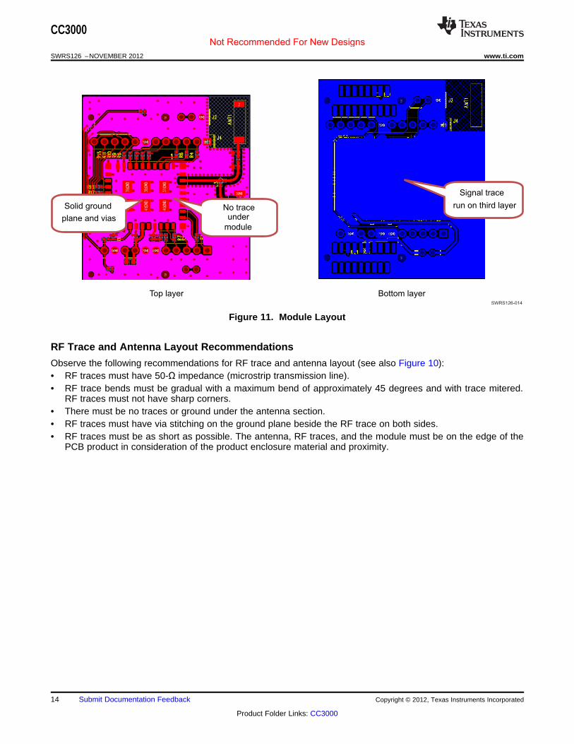
Module Layout Recommendations
Observe the following module layout recommendations (see also Figure 11):• Have a solid ground plane and ground vias under the module for stable system and thermal dissipation.• Do not run signal traces underneath the module on a layer where the module is mounted.• Signal traces can be run on a third layer under the solid ground layer and beneath the module mounting
layer.
Copyright © 2012, Texas Instruments Incorporated Submit Documentation Feedback 13
Product Folder Links: CC3000
Not Recommended For New Designs
SWRS126-014
Solid ground
plane and vias
No traceunder
module
Signal trace
run on third layer
Top layer Bottom layer
CC3000
SWRS126 –NOVEMBER 2012 www.ti.com
Figure 11. Module Layout
RF Trace and Antenna Layout Recommendations
Observe the following recommendations for RF trace and antenna layout (see also Figure 10):• RF traces must have 50-Ω impedance (microstrip transmission line).• RF trace bends must be gradual with a maximum bend of approximately 45 degrees and with trace mitered.
RF traces must not have sharp corners.• There must be no traces or ground under the antenna section.• RF traces must have via stitching on the ground plane beside the RF trace on both sides.• RF traces must be as short as possible. The antenna, RF traces, and the module must be on the edge of the
PCB product in consideration of the product enclosure material and proximity.
14 Submit Documentation Feedback Copyright © 2012, Texas Instruments Incorporated
Product Folder Links: CC3000
Not Recommended For New Designs
PACKAGE OPTION ADDENDUM
www.ti.com 25-Apr-2017
Addendum-Page 1
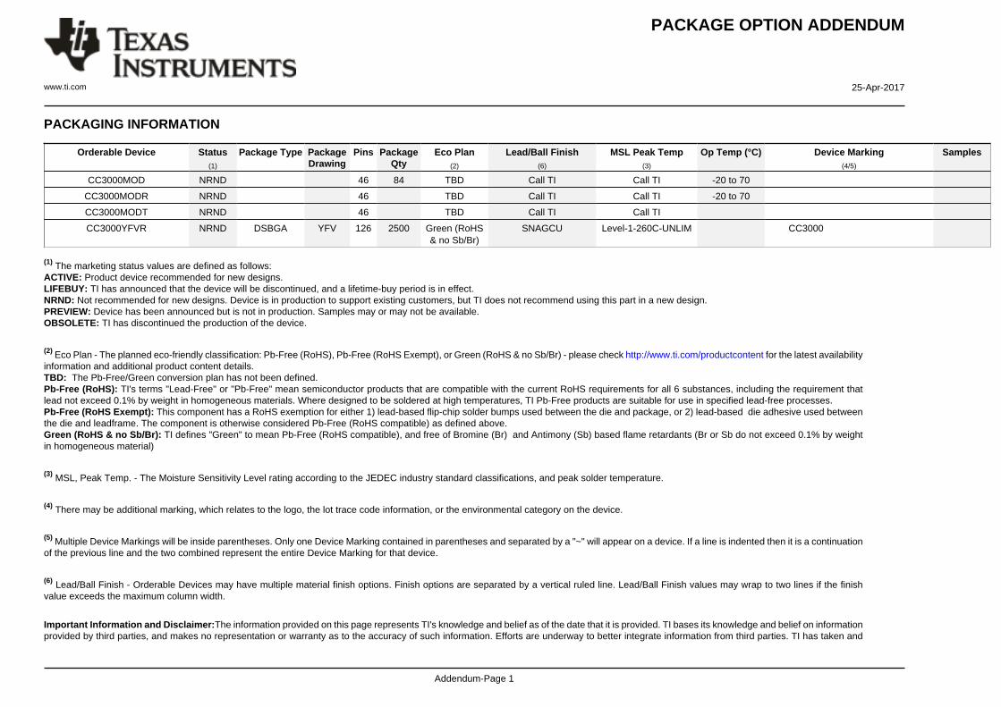
PACKAGING INFORMATION
Orderable Device Status(1)
Package Type PackageDrawing
Pins PackageQty
Eco Plan(2)
Lead/Ball Finish(6)
MSL Peak Temp(3)
Op Temp (°C) Device Marking(4/5)
Samples
CC3000MOD NRND 46 84 TBD Call TI Call TI -20 to 70
CC3000MODR NRND 46 TBD Call TI Call TI -20 to 70
CC3000MODT NRND 46 TBD Call TI Call TI
CC3000YFVR NRND DSBGA YFV 126 2500 Green (RoHS& no Sb/Br)
SNAGCU Level-1-260C-UNLIM CC3000
(1) The marketing status values are defined as follows:ACTIVE: Product device recommended for new designs.LIFEBUY: TI has announced that the device will be discontinued, and a lifetime-buy period is in effect.NRND: Not recommended for new designs. Device is in production to support existing customers, but TI does not recommend using this part in a new design.PREVIEW: Device has been announced but is not in production. Samples may or may not be available.OBSOLETE: TI has discontinued the production of the device.
(2) Eco Plan - The planned eco-friendly classification: Pb-Free (RoHS), Pb-Free (RoHS Exempt), or Green (RoHS & no Sb/Br) - please check http://www.ti.com/productcontent for the latest availabilityinformation and additional product content details.TBD: The Pb-Free/Green conversion plan has not been defined.Pb-Free (RoHS): TI's terms "Lead-Free" or "Pb-Free" mean semiconductor products that are compatible with the current RoHS requirements for all 6 substances, including the requirement thatlead not exceed 0.1% by weight in homogeneous materials. Where designed to be soldered at high temperatures, TI Pb-Free products are suitable for use in specified lead-free processes.Pb-Free (RoHS Exempt): This component has a RoHS exemption for either 1) lead-based flip-chip solder bumps used between the die and package, or 2) lead-based die adhesive used betweenthe die and leadframe. The component is otherwise considered Pb-Free (RoHS compatible) as defined above.Green (RoHS & no Sb/Br): TI defines "Green" to mean Pb-Free (RoHS compatible), and free of Bromine (Br) and Antimony (Sb) based flame retardants (Br or Sb do not exceed 0.1% by weightin homogeneous material)
(3) MSL, Peak Temp. - The Moisture Sensitivity Level rating according to the JEDEC industry standard classifications, and peak solder temperature.
(4) There may be additional marking, which relates to the logo, the lot trace code information, or the environmental category on the device.
(5) Multiple Device Markings will be inside parentheses. Only one Device Marking contained in parentheses and separated by a "~" will appear on a device. If a line is indented then it is a continuationof the previous line and the two combined represent the entire Device Marking for that device.
(6) Lead/Ball Finish - Orderable Devices may have multiple material finish options. Finish options are separated by a vertical ruled line. Lead/Ball Finish values may wrap to two lines if the finishvalue exceeds the maximum column width.
Important Information and Disclaimer:The information provided on this page represents TI's knowledge and belief as of the date that it is provided. TI bases its knowledge and belief on informationprovided by third parties, and makes no representation or warranty as to the accuracy of such information. Efforts are underway to better integrate information from third parties. TI has taken and

PACKAGE OPTION ADDENDUM
www.ti.com 25-Apr-2017
Addendum-Page 2
continues to take reasonable steps to provide representative and accurate information but may not have conducted destructive testing or chemical analysis on incoming materials and chemicals.TI and TI suppliers consider certain information to be proprietary, and thus CAS numbers and other limited information may not be available for release.
In no event shall TI's liability arising out of such information exceed the total purchase price of the TI part(s) at issue in this document sold by TI to Customer on an annual basis.
IMPORTANT NOTICE
Texas Instruments Incorporated (TI) reserves the right to make corrections, enhancements, improvements and other changes to itssemiconductor products and services per JESD46, latest issue, and to discontinue any product or service per JESD48, latest issue. Buyersshould obtain the latest relevant information before placing orders and should verify that such information is current and complete.TI’s published terms of sale for semiconductor products (http://www.ti.com/sc/docs/stdterms.htm) apply to the sale of packaged integratedcircuit products that TI has qualified and released to market. Additional terms may apply to the use or sale of other types of TI products andservices.Reproduction of significant portions of TI information in TI data sheets is permissible only if reproduction is without alteration and isaccompanied by all associated warranties, conditions, limitations, and notices. TI is not responsible or liable for such reproduceddocumentation. Information of third parties may be subject to additional restrictions. Resale of TI products or services with statementsdifferent from or beyond the parameters stated by TI for that product or service voids all express and any implied warranties for theassociated TI product or service and is an unfair and deceptive business practice. TI is not responsible or liable for any such statements.Buyers and others who are developing systems that incorporate TI products (collectively, “Designers”) understand and agree that Designersremain responsible for using their independent analysis, evaluation and judgment in designing their applications and that Designers havefull and exclusive responsibility to assure the safety of Designers' applications and compliance of their applications (and of all TI productsused in or for Designers’ applications) with all applicable regulations, laws and other applicable requirements. Designer represents that, withrespect to their applications, Designer has all the necessary expertise to create and implement safeguards that (1) anticipate dangerousconsequences of failures, (2) monitor failures and their consequences, and (3) lessen the likelihood of failures that might cause harm andtake appropriate actions. Designer agrees that prior to using or distributing any applications that include TI products, Designer willthoroughly test such applications and the functionality of such TI products as used in such applications.TI’s provision of technical, application or other design advice, quality characterization, reliability data or other services or information,including, but not limited to, reference designs and materials relating to evaluation modules, (collectively, “TI Resources”) are intended toassist designers who are developing applications that incorporate TI products; by downloading, accessing or using TI Resources in anyway, Designer (individually or, if Designer is acting on behalf of a company, Designer’s company) agrees to use any particular TI Resourcesolely for this purpose and subject to the terms of this Notice.TI’s provision of TI Resources does not expand or otherwise alter TI’s applicable published warranties or warranty disclaimers for TIproducts, and no additional obligations or liabilities arise from TI providing such TI Resources. TI reserves the right to make corrections,enhancements, improvements and other changes to its TI Resources. TI has not conducted any testing other than that specificallydescribed in the published documentation for a particular TI Resource.Designer is authorized to use, copy and modify any individual TI Resource only in connection with the development of applications thatinclude the TI product(s) identified in such TI Resource. NO OTHER LICENSE, EXPRESS OR IMPLIED, BY ESTOPPEL OR OTHERWISETO ANY OTHER TI INTELLECTUAL PROPERTY RIGHT, AND NO LICENSE TO ANY TECHNOLOGY OR INTELLECTUAL PROPERTYRIGHT OF TI OR ANY THIRD PARTY IS GRANTED HEREIN, including but not limited to any patent right, copyright, mask work right, orother intellectual property right relating to any combination, machine, or process in which TI products or services are used. Informationregarding or referencing third-party products or services does not constitute a license to use such products or services, or a warranty orendorsement thereof. Use of TI Resources may require a license from a third party under the patents or other intellectual property of thethird party, or a license from TI under the patents or other intellectual property of TI.TI RESOURCES ARE PROVIDED “AS IS” AND WITH ALL FAULTS. TI DISCLAIMS ALL OTHER WARRANTIES ORREPRESENTATIONS, EXPRESS OR IMPLIED, REGARDING RESOURCES OR USE THEREOF, INCLUDING BUT NOT LIMITED TOACCURACY OR COMPLETENESS, TITLE, ANY EPIDEMIC FAILURE WARRANTY AND ANY IMPLIED WARRANTIES OFMERCHANTABILITY, FITNESS FOR A PARTICULAR PURPOSE, AND NON-INFRINGEMENT OF ANY THIRD PARTY INTELLECTUALPROPERTY RIGHTS. TI SHALL NOT BE LIABLE FOR AND SHALL NOT DEFEND OR INDEMNIFY DESIGNER AGAINST ANY CLAIM,INCLUDING BUT NOT LIMITED TO ANY INFRINGEMENT CLAIM THAT RELATES TO OR IS BASED ON ANY COMBINATION OFPRODUCTS EVEN IF DESCRIBED IN TI RESOURCES OR OTHERWISE. IN NO EVENT SHALL TI BE LIABLE FOR ANY ACTUAL,DIRECT, SPECIAL, COLLATERAL, INDIRECT, PUNITIVE, INCIDENTAL, CONSEQUENTIAL OR EXEMPLARY DAMAGES INCONNECTION WITH OR ARISING OUT OF TI RESOURCES OR USE THEREOF, AND REGARDLESS OF WHETHER TI HAS BEENADVISED OF THE POSSIBILITY OF SUCH DAMAGES.Unless TI has explicitly designated an individual product as meeting the requirements of a particular industry standard (e.g., ISO/TS 16949and ISO 26262), TI is not responsible for any failure to meet such industry standard requirements.Where TI specifically promotes products as facilitating functional safety or as compliant with industry functional safety standards, suchproducts are intended to help enable customers to design and create their own applications that meet applicable functional safety standardsand requirements. Using products in an application does not by itself establish any safety features in the application. Designers mustensure compliance with safety-related requirements and standards applicable to their applications. Designer may not use any TI products inlife-critical medical equipment unless authorized officers of the parties have executed a special contract specifically governing such use.Life-critical medical equipment is medical equipment where failure of such equipment would cause serious bodily injury or death (e.g., lifesupport, pacemakers, defibrillators, heart pumps, neurostimulators, and implantables). Such equipment includes, without limitation, allmedical devices identified by the U.S. Food and Drug Administration as Class III devices and equivalent classifications outside the U.S.TI may expressly designate certain products as completing a particular qualification (e.g., Q100, Military Grade, or Enhanced Product).Designers agree that it has the necessary expertise to select the product with the appropriate qualification designation for their applicationsand that proper product selection is at Designers’ own risk. Designers are solely responsible for compliance with all legal and regulatoryrequirements in connection with such selection.Designer will fully indemnify TI and its representatives against any damages, costs, losses, and/or liabilities arising out of Designer’s non-compliance with the terms and provisions of this Notice.
Mailing Address: Texas Instruments, Post Office Box 655303, Dallas, Texas 75265Copyright © 2017, Texas Instruments Incorporated