chapter 15: materials and emerging research materials · chapter 15: materials and emerging...
TRANSCRIPT

2019 Edition
Chapter 15: Materials and Emerging Research Materials
http://eps.ieee.org/hir
We acknowledge with gratitude the use of material and figures in this Roadmap that are excerpted from original sources. Figures & tables should be re-used only with the permission of the original source.
The HIR is devised and intended for technology assessment only and is without regard to any commercial considerations pertaining to individual products or equipment.

October, 2019 Table of Contents
HIR Version 1.0 (eps.ieee.org/hir) Page ii Heterogeneous Integration Roadmap
Table of Contents
CHAPTER 1: HETEROGENEOUS INTEGRATION ROADMAP: OVERVIEW .......................................................................... 1
CHAPTER 2: HIGH PERFORMANCE COMPUTING AND DATA CENTERS ............................................................................. 1
CHAPTER 3: THE INTERNET OF THINGS (IOT) .................................................................................................................. 1
CHAPTER 4: MEDICAL, HEALTH & WEARABLES ............................................................................................................... 1
CHAPTER 5: AUTOMOTIVE ............................................................................................................................................ 1
CHAPTER 6: AEROSPACE AND DEFENSE ......................................................................................................................... 1
CHAPTER 7: MOBILE ...................................................................................................................................................... 1
CHAPTER 8: SINGLE CHIP AND MULTI CHIP INTEGRATION .............................................................................................. 1
CHAPTER 9: INTEGRATED PHOTONICS ........................................................................................................................... 1
CHAPTER 10: INTEGRATED POWER ELECTRONICS .......................................................................................................... 1
CHAPTER 11: MEMS AND SENSOR INTEGRATION ........................................................................................................... 1
CHAPTER 12: 5G COMMUNICATIONS ............................................................................................................................. 1
CHAPTER 13: CO DESIGN FOR HETEROGENEOUS INTEGRATION ..................................................................................... 1
CHAPTER 14: MODELING AND SIMULATION .................................................................................................................. 1
CHAPTER 15: MATERIALS AND EMERGING RESEARCH MATERIALS ................................................................................. 1
CHAPTER 16: EMERGING RESEARCH DEVICES ................................................................................................................ 1
CHAPTER 17: TEST TECHNOLOGY ................................................................................................................................... 1
CHAPTER 18: SUPPLY CHAIN .......................................................................................................................................... 1
CHAPTER 19: SECURITY ................................................................................................................................................. 1
CHAPTER 20: THERMAL ................................................................................................................................................. 1
CHAPTER 21: SIP AND MODULE SYSTEM INTEGRATION ................................................................................................. 1
CHAPTER 22: INTERCONNECTS FOR 2D AND 3D ARCHITECTURES ................................................................................... 1
CHAPTER 23: WAFER‐LEVEL PACKAGING (WLP) ............................................................................................................. 1
To download additional chapters, please visit
http://eps.ieee.org/hir

October, 2019 Materials and Emerging Research Materials
HIR version 1.0 (eps.ieee.org/hir) Chapter 15, Page 1 Heterogeneous Integration Roadmap
Chapter 15: Materials and Emerging Research Materials
This chapter is in preparation, and will be integrated into the Roadmap at Version 1.1, planned for the end of 2019.
In its place is the following summary and a series of slides giving the current status of current materials, and emerging research materials, and some information that is relevant to the progress needed over the next 10 to 15 years.
Executive Summary
The focus of the Materials section is on the evolution of materials that can provide a wider range of properties for conductors, semiconductors and insulators to meet demands for lower cost, reduced power, higher thermal density and higher performance. It will address requirements identified by other HIR TWGs. The time horizon is for new materials that will be in production within 10 years. Supply chain requirements will be included in collaboration with the Supply Chain TWG.
The Emerging Research Materials section focus is on the revolution in materials required for new device types, and disruptive improvements that can replace the conductors, insulators, semiconductors and optical materials in current device architectures. The time horizon is for new materials that will be in volume production beyond 10 years and up to 25 years.
The scope of the Chapter includes:
Supporting the HIR working groups with new materials required to meet the difficult challenges they identify.
Enabling disruptive changes in capability of emerging devices such as quantum computing, biomedical systems, flexible electronics, etc., through novel materials.
Expanding the range of properties available through new classes of composite materials combining novel matrix materials with nano-materials.
Defining the difficult challenges requires close collaboration with other TWGs both within and outside of this Roadmap.
October, 2019 Materials and Emerging Research Materials
HIR version 1.0 (eps.ieee.org/hir) Chapter 15, Page 2 Heterogeneous Integration Roadmap
TWG Chair: Bill Bottoms
Materials and Emerging Research Materials Chapter ScopeThe Materials Sub‐chapter focus is on the evolution of materials providing a wider range of properties for conductors,semiconductors and insulators to meet demands for lower cost, reduced power, higher thermal density and higherperformance. The Scope will address requirements identified by other HIR TWGS. The time horizon is for newmaterials that will be in production within 10 years. Supply chain requirements will be included in collaboration withthe Supply Chain TWG.
The Emerging Research Materials Sub‐chapter focus is on the revolution in materials required for new device types,and disruptive improvements replacing the conductors, insulators, semiconductors and optical materials in currentdevice architectures. The time horizon is for new materials that will be in volume production beyond 10 years and upto 25 years.
The scope of the Chapter includes:
• Supporting the HIR working groups with new materials required to meet the difficult challenges they identify.
• Enabling disruptive changes in capability of emerging devices such as quantum computing, biomedical systems, flexible electronics, etc, through novel materials
• Expanding the range of properties available through new classes of composite materials combining novel matrix materials with nano‐materials
Defining the difficult challenges requires close collaboration with other TWGs both in and outside of HIR.
1
2

October, 2019 Materials and Emerging Research Materials
HIR version 1.0 (eps.ieee.org/hir) Chapter 15, Page 3 Heterogeneous Integration Roadmap
Heterogeneous Integration by Materials
Conductors• Nanomaterials (CNT, graphene, nanowires)
• Metals (Cu, Al, W, Ag, Co, etc.)
• Composites
Dielectrics• Oxides
• Polymers
• Porous materials
• Composites
Semiconductors• Elemental (Si, Ge)
• Compounds (IIIV, IIVI, tertiary)
• Polymers
Materials Parameters must be compatible with each other for processing and operation: Cost
CTE differential
Thermal conductivity
Fracture toughness
Modulus
Processing temperature
Interfacial adhesion
Operating temperature
Breakdown field strength
Identify integrated high k dielectrics with Equivalent Oxide Thickness <0.5nm, high breakdown field and low leakage
Identify integrated contact structures that have ultralow contact resistance
Achieving high hole mobility indirect band gap materials in FET structures
Achieving high electron mobility in Ge with low contact resistance in FET structures
Achieving a bandgap in graphene suitable for FET structures
Multiferroic with Curie temperature >400K and high remnant magnetization to >400K
Synthesis of single wall CNTs with tight distribution of bandgap and mobility
Electrical control of the electron correlation, ex. Mott transition, Spin dynamics
Simultaneously achieve package polymer CTE, modulus, electrical, thermal properties, with moisture and ion diffusion barriers for
low stress packaging at use case temperature
Thermal interface materials with low interface thermal resistance and high thermal conductivity with desired electrical and
mechanical properties.
Nanosolders compatible with <200C assembly, multiple reflows, high strength, high thermal and electrical conductivity and high
electromigration resistance.
NanoInks that can be printed as die attach adhesives with required electrical, mechanical, thermal, interface,and reliability
properties.
NanoInks that can be printed as conductors, via hole fillers, solders, or die attach adhesives with required electrical, mechanical,
thermal, interface and reliability properties.
Materials and Emerging Research Material Difficult Challenges
Difficult Challenges 2018‐2028
Achieving desired properties in
integrated structures
Difficult Materials Challenges 2019-2029 (1)
3
4

October, 2019 Materials and Emerging Research Materials
HIR version 1.0 (eps.ieee.org/hir) Chapter 15, Page 4 Heterogeneous Integration Roadmap
thermal, interface and reliability properties.
High mobility transition metal dichalcogenides TMD with unpinned Fermi level and low resistance ohmic contacts.
High electron mobility in Ge with unpinned Fermi level and low resistance ohmic contacts.
High mobility nanowires with unpinned Fermi level and low interface resistance.
Graphene with a bandgap suitable for FET structures, high mobility, and unpinned Fermi level at dielectric interfaces.
Complex metal oxides with unpinned Fermi levels
Characterization of electrical properties of molecule / metal contact interfaces (i.e. Pentacene/Au)
Characterization of electrical properties of embedded nano contact interfaces (i.e. CNT/Metal )
CNTs with low resistance contacts on both ends
Characterization for density of dislocations and anti‐phase boundary generating interface between Ge/III‐V channel materials and
Si.
Dopant placement and activation i.e. deterministic doping with desired number at precise location for Vth control and S/D
formation in Si as well as alternate materials.
HVM compatible methods to place dopants in predetermined positions with minimal damage to the semiconductor.
Manufacturing and purification methodologies of single wall CNTs to achieve required purity levels (pure semiconductor with
bandgap)
Identify DSA process simplification methodologies that can achieve required overlay requirements.
Wafer scale growth of high quality graphene with desired process conditions (ex. Low temperature growth on metal or insulator)
Controlling edge‐termination / molecular absorption to graphene to achieve required bandgap.
Synthesis or assembly of CNTs in predefined locations and directions with controlled diameters, chirality and site‐density.
III‐V: Correlation between antiphase domains and electrical properties.
Control defects in carbon nanotubes.
Control defects in growth and processing of graphene.
Control concentration and locations of cation and anion defects in complex metal oxides.
Control precipitation in ferromagnetic semiconductors.
Characterization for density of dislocations and anti‐phase boundary generating interface between Ge/III‐V channel materials and
Si.
Identifying manufacturable
methodologies to enable
deterministic fabrication with
required property control
Characterize and control
coupled properties of embedded
materials and their interfaces
Difficult Materials Challenges 2019-2029 (2)
Si.
Biocompatible functional materials
DSA for Litho Extension: Efficient CAD models to enable translating design features to guide structures on photomasks.
DSA for Litho Extension: Registration of self‐assembled patterning materials in desired locations with control of geometry,
conformation, interface roughness, and defects
DSA for Litho Extension: Achieve realistic device pattern with reduced pattern roughness and defects
Demonstrate self assembly's ability to deterministically control locations of dopants conformally on 3D structures
Control of Self‐assembly
processes to achieve desired
properties reproducibly
Difficult Materials Challenges 2019-2029 (3)
5
6

October, 2019 Materials and Emerging Research Materials
HIR version 1.0 (eps.ieee.org/hir) Chapter 15, Page 5 Heterogeneous Integration Roadmap
Complex Oxides: Control of oxygen vacancy formation at metal interfaces and interactions of electrodes with oxygen and
vacancies
Switching mechanism of atomic switch: Improvements in switching speed, cyclic endurance, uniformity of the switching bias
voltage and resistances both for the on‐state and the off‐state.
Nano‐Carbon / metal functional junction, such as new switch, by using electrochemical reactions
Molecular device fabrication with precise control using electrochemical reactions
Development of the method to evaluate the validity of the measurement result for each ERM
Electrical and thermal properties of each carbon nanotube
Nanowire characterization of mobility, carrier density, interface states, and dielectric fixed charge effects
Graphene and TMD mobility and carrier concentration
Complex metal oxide characterization of carrier density, dielectric and magnetic properties
Spin materials: characterization of spin, magnetic and electrical properties and correlation to nanostructure
Characterization of electrical properties of embedded nano contact interfaces (ex. CNT/Metal )
Evaluating material properties in realistic device structures
Nanoscale observation of the magnetic domain structure, for example, the domain in STT‐RAM under the magnetic field, i.e., the
dynamic operation
Electric field control of the
electrochemical reaction in a
nanoscaled device and at an
interface
Difficult Challenges 2029‐2043
Metrology to characterize
structure and properties of
materials at the nanometer
scale
Difficult Materials Challenges 2029-2043 (1)
dynamic operation
CNT vacancy and interstitial ordering around dopants
Nanowires: Characterization of vacancies, interstitials and dopants within the NW and at interfaces to dielectrics
Graphene: Characterization of edge defects, vacancies and interstitials within the material and at interfaces
Metal nanoparticles: Native oxide interface and crystal defects in the nanoparticle
Complex Oxides: Location of oxygen vacancies and the valence state of the metal ions
Spin materials: characterization of vacancies in spin tunnel barriers, and defects within magnetic materials and at their interfaces
Evaluating material properties IN realistic nm scale devices
Characterization of edge structure and termination with atomic resolution (ex. Graphene nano ribbon, TMD, etc. )
Linkage between different scales in time, space, and energy bridging non‐equilibrium phenomena to equilibrium phenomena
Transferable simulation tools for many kinds of materials
Development of platform for different simulation tools, such as TCAD and ab‐initio calculations
Nanowires: Simulation of growth and defect formation within and at interfaces
CNTs: Simulation of growth and correlation to bandgap
Graphene: Simulation of synthesis, edge defects, vacancies, interstitials, interfacial bonding, and substrate interactions.
Atomistic simulation of interfaces for determining Fermi level location and resulting contact resistivity
Nanoparticles: Simulation of growth and correlation to structure and defects
Complex Oxides: Multiscale simulation of vacancy formation, effect on metal ion valence state and effect of the space charge layer
Spin: Improved models for multiscale simulation of spin properties within materials and at their interfaces.
Metrology to characterize
defects at the nanometer scale
with atomic resolution
Accurate multiscale simulation
for predictions of unit processes
the resulting structure,
properties and device
performance.
Difficult Materials Challenges 2029-2043 (2)
7
8

October, 2019 Materials and Emerging Research Materials
HIR version 1.0 (eps.ieee.org/hir) Chapter 15, Page 6 Heterogeneous Integration Roadmap
Geometry, conformation, and interface roughness in molecular and self‐assembled structures
Device structure‐related properties, such as ferromagnetic spin and defects
Dopant location and device variability
Integration on CMOS Platforms
Integration with flexible electronics
Biocompatible functional materials
Robust long‐term biotic‐abiotic interfaces that avoid biofouling isses
Leveraging convergent materials experetise in adjacent sectors
Fundamental thermodynamic
stability and fluctuations of
materials and structures
Materials and processes that
enable monolithically
integrated complex
functionality
Difficult Materials Challenges 2029-2043 (3)
New Conductors and Joining Processes Have Been Known For
Years But Are Not Yet Used In Volume Production
Work in Progress. Please do not distribute without permission of HIR IRC
9
10

October, 2019 Materials and Emerging Research Materials
HIR version 1.0 (eps.ieee.org/hir) Chapter 15, Page 7 Heterogeneous Integration Roadmap
Warpage For Ever Thinner Layers
Solutions for warpage are known and demonstrated but not integrated for production
• Reduced copper CTE (4.5 rather than 17)
• Low‐modulus dielectrics
• No underfill
• Direct interconnect bonding
• All joining processing done at or near use‐case temperature
Warpage For Ever Thinner Layers
Combining These Materials And Processes Solves Stress and Warpage Issues And
Improves Performance
11
12

October, 2019 Materials and Emerging Research Materials
HIR version 1.0 (eps.ieee.org/hir) Chapter 15, Page 8 Heterogeneous Integration Roadmap
Examples Of New Materials With Proof Of Concept
Cobalt & Cobalt/Copper, in use today. Contact resistance reduced 1.5X,Line resistance down 60%. Intel
Shape shifting switch in 2D MoTe2 X . Zhang, Berkeley
Thermal ManagementKey elements of thermal management
• Don’t make heat in the first place (device design, low frequency‐high parallelism, subthreshold operation, reduced interconnect distance )
• Lower‐resistance conductors
• Lower operating voltage
• Lower‐k dielectrics
• Active voltage control
• Rapid shut down and power up (sub‐nanosecond. GaN)
• Improved heat sink materials and design
13
14

October, 2019 Materials and Emerging Research Materials
HIR version 1.0 (eps.ieee.org/hir) Chapter 15, Page 9 Heterogeneous Integration Roadmap
Thermal Management Reaching Limits of Imagination
Source: Raytheon, Avi Bar‐Cohen
Diamond Microchannel Bonded to GaN Amplifier
Source: Raytheon, Avi Bar‐Cohen
15
16
October, 2019 Materials and Emerging Research Materials
HIR version 1.0 (eps.ieee.org/hir) Chapter 15, Page 10 Heterogeneous Integration Roadmap
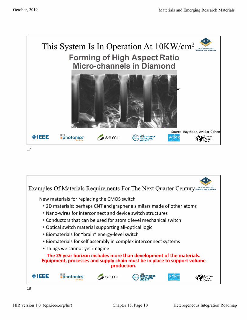
This System Is In Operation At 10KW/cm2
Source: Raytheon, Avi Bar‐Cohen
Examples Of Materials Requirements For The Next Quarter Century
New materials for replacing the CMOS switch
• 2D materials: perhaps CNT and graphene similars made of other atoms
• Nano‐wires for interconnect and device switch structures• Conductors that can be used for atomic level mechanical switch
• Optical switch material supporting all‐optical logic
• Biomaterials for “brain” energy‐level switch
• Biomaterials for self assembly in complex interconnect systems
• Things we cannot yet imagine
The 25 year horizon includes more than development of the materials. Equipment, processes and supply chain must be in place to support volume
production.
17
18

October, 2019 Materials and Emerging Research Materials
HIR version 1.0 (eps.ieee.org/hir) Chapter 15, Page 11 Heterogeneous Integration Roadmap
2D Class Of Materials Can Support Many Device Types
Nano-Infused Ceramic Self-Report For Self-reporting Structural Sensors (Composite Materials)
CeramicGrapheneCeramic
19
20

October, 2019 Materials and Emerging Research Materials
HIR version 1.0 (eps.ieee.org/hir) Chapter 15, Page 12 Heterogeneous Integration Roadmap
Artificial Intelligence May Design New Materials
The MIT system uses statistical methods that provide a natural mechanism for generating original recipes, which suggest alternative recipes for known materials that accord well with real recipes.
AI and Big Data can learn to design applications specific materials
A machine‐learning system analyzes materials “recipes” using an autoencoder. If successfully trained, the system will capture the data’s characteristics.Image: Chelsea Turner/MIT
Summary• The Materials Sub‐chapter identifies difficult challenges and potential solutions and identifies probable date for volume production in our Tables for selected examples.
• The Emerging Research Materials Sub‐Chapter identifies difficult challenges and, where possible, potential solutions for selected examples. There is no prediction of the date for volume production.
Our objective is to accelerate the pace of progress by stimulating pre‐competitive collaboration.
21
22