chapter 2 - california institute of...
TRANSCRIPT

15
Chapter 2
Ultrafast Electron Crystallography:
Principles and Dynamics†
†Part of this chapter was adapted from D.-S. Yang, N. Gedik, A. H. Zewail, J. Phys. Chem. C 111, 4889 (2007).

16
Introduction
The geometric nature in the structure analysis of a molecule or a crystal by
electron diffraction shares a high degree of similarity with that by x-ray diffraction. The
geometrical theory originally developed for x-ray crystallography can, therefore, be used
in electron crystallography, and its relevance to our technique is described in this chapter.
The major dissimilarities between these two diffraction methods originate from the
different radiation–matter interactions. Because x-ray is an electromagnetic wave, its
scattering—Thomson scattering if the energy is conserved—is caused by the (polarizable)
electron density in the electron shells of the atoms; atomic nuclei are very poorly affected
by the electromagnetic field and, hence, invisible to such radiation. Consequently,
structure analysis of x-ray diffraction deals with the distribution of electron density that is
often concentrated around the nuclei. For electron interaction with matter, however, it is
the Coulomb force that governs the scattering because electrons are charged particles, and
as a result, the electrostatic potential due to both the positively charged atomic nuclei and
their electron clouds should be considered. On the basis of the different interactions
involved, the average magnitude of the atomic scattering amplitude of electrons is about
103 times that of x-ray, leading to a ratio of 106 for the scattered intensities (1). Therefore,
electrons are strongly scattered by matter, which grants electron diffraction with a higher
sensitivity for the probing of nanometer-scale and interfacial structures and in the
detection of small structural changes in time.
Before the presentation of the geometrical theory, a quick summary for
quantitative description of the intensities of the scattered beams is given here. Derivation
of the kinematic (elastic) scattering theory for electron diffraction starts from the
time-dependent Schrödinger equation and considers a propagating plane wave for the

17
incident electrons (1-3),
trkiAtr i0 exp, (1)
where A denotes the amplitude, ik
the incidence wavevector, and the angular
frequency. The relativistic effect needs to be taken into account for highly accelerated
electrons,
200
20
240
200 cmcpcmeV (2)
where V0 is the acceleration voltage (in volt), m0 the electron’s rest mass, p the electron’s
momentum, and c0 is the speed of light. According to the de Broglie relation, the
electron’s wavelength () is equal to h/p and, therefore, can be expressed (in Å) by (4)
06
0200000 109785.0126.12212 VVcmeVeVmh . (3)
With the use of the mathematical tool of Green’s function, the scattered wave derived in
the asymptotic limit for large-L, far-field detection (i.e., Fraunhofer diffraction that is
typically the case for crystallographic measurements) and under the first Born
approximation is given by (1-3)
rrkkirUL
eAL
ikL 3
iS dexpπ4
, (4)
where k
is the outgoing wavevector ( | k
| = | ik
| ) along the direction of L
,
rVemrU
22 is the reduced potential associated with the electrostatic potential
of the scattering object, rV
, and the integration runs over the occupied volume.
Therefore, the kinematic theory of electron scattering (Eq. 4) can be deduced with
the use of the theory of Fourier integrals, defining the relative scattering amplitude
rrsirUsf 3dexp
π4
1 (5)
with the momentum transfer vector

18
ikks
. (6)
The observed diffraction intensities, 2
S LLI
, are therefore in proportion to 2sf
(1, 2). The detailed structure in the potential of the specimen (thereby the spatial
arrangement of atoms) is given by
srsisfrU 3
3dexpπ4
π8
1. (7)
Thus, these results provide the theoretical basis for the geometrical theory considering the
periodic lattice structure in real space and its Fourier transform, the periodic reciprocal
lattice, in reciprocal (k) space.
If rU
is substituted by a sum of reduced atomic potentials, jj rrU
a
(displaced according to their central positions in a crystal), where j refers to the jth atom,
j
jj rrUrU a , (8)
Equation 5 can be rewritten as
jj
jjjjj
j rsisfrrrsirrUrsisf expdexpexp
π4
1 3a (9)
with the definition of the atomic scattering factor, sf j
, being
rrsirUsf jj
3a dexpπ4
1. (10)
The assumption here is that rU j
a in a crystal is approximately the same as that for an
isolated atom (i.e., the valence electrons affect the electron scattering to a very minor
extent). Although the absolute values of diffraction intensities may show small deviation
from the kinematic theory described above, it will become clear that, from the various
studies successfully made, the kinematic approximation is capable of capturing the most
important information from the observed diffraction changes in time and, therefore,
suitable for the structural dynamics studies using electron diffraction.

19
Fig. 1. Schematic of the methodology of UEC in the reflection geometry. The
relationship between real and reciprocal lattices and Ewald construction for the formation
of diffraction patterns are shown (see Text and Figs. 2 to 4 for details). The temporal and
spatial resolutions of UEC are achieved by varying the delay time between the electron
probe and initiating heating pulses (upper left), and the recording of the diffraction
patterns at different times.

20
From the discussion below, it is straightforward to see that the geometrical theory
for high-energy electron diffraction is much simpler than that for x-ray diffraction
because of the very short electron wavelength used. Ultrafast electron crystallography
(UEC), a time-resolved electron diffraction technique for condensed-matter studies, can
be performed in two modes, reflection or transmission geometry. The implementation in
the reflection geometry (Fig. 1) enables us to determine time-resolved nonequilibrium
structures of a crystal surface region or adsorbate near the interface, and also their
equilibrium structures at steady state. The transmission geometry allows the detection of
structures and dynamics of nanometer-scale specimens. In what follows, the theoretical
foundation to determine structures, their inhomogeneity, and the corresponding temporal
evolution is examined. A typical diffraction image may show a pattern of Bragg spots,
streaks, Debye−Scherrer rings, Kikuchi lines or bands, or a combination of these with a
scattering background. By monitoring and comparing the changes of different diffraction
features, such as position, intensity, width, and shape, we can obtain a more complete
picture of structural dynamics. Experimental test cases (gold and silicon) are also
provided in this chapter to illustrate the principles invoked.
A. Equilibrium Structures
A.1. Diffraction in Reflection
Spots or rings in an electron diffraction pattern are the result of the constructive
interference of scattered waves from different lattice points. In UEC, the electrons have
large kinetic energy (eV0 = 30 keV) and therefore a small de Broglie wavelength,
~ 0.07 Å from Eq. 3, which is a few percent of a typical atomic spacing (the reason
behind the resolution of interatomic distances through diffraction). For elastic scattering,
the criterion of constructive interference is described by the Bragg condition:

21
Fig. 2. (a) Vectorial representation for the elastic scattering process. The incidence angle
i = /2 and the scattering vector s
are shown. (b) Upper: The von Laue condition of
constructive interference. The phase difference between two outgoing waves scattered by
two atoms separated by R
is indicated by the curly brackets. Lower: Comparison of the
von Laue and Bragg formulations for constructive interference conditions. Note that s
is parallel to the interplanar distance d under investigation (i.e., perpendicular to the
Bragg planes under probing), and any vector of the real lattice has a projection onto the
s
direction to be an integer multiple of d.
n = 2d sin(/2), (11)
which is simply the result of considering crystal planes of reflections; n is the order of
diffraction, d is the distance between adjacent parallel crystal planes, and is the total
angle of deflection from the initial beam. Because is known, in principle, if n is known,
the measurement of gives d. In practice, the interplanar distance d can be obtained from
rocking curves by changing the incidence angle and recording spots of two consecutive
orders, n and n + 1, thus removing the need for assigning the absolute precise magnitudes
of n and (see below).

22
The equivalent picture given by the von Laue formulation considers the
geometrical phase shifts of the scatterers themselves. For elastic scattering, because the
wavevectors of the incident and scattered electrons ( ik
and k
) have the same amplitude
(| k
| = | ik
| = 2/), the scattering vector (Eq. 6) yields s = | s
| = (4/)sin(/2); see
Fig. 2a for the vectorial representation and Appendix A for the convention used. The
phase matching of the scattered waves from all scatterers is required for constructive
interference (Eq. 9), which means that for all vectors R
connecting atoms of the Bravais
lattice in real space, the Laue condition is satisfied when 1exp Rsi
, or equivalently,
when π2mRs
where m is an integer (Fig. 2b, upper). It is noted that the same
equation leads to the Bragg condition by substituting the amplitude of s
and
recognizing that the projection of R
along the s
direction equals to m times the
interplanar distance d (Fig. 2b, lower). Therefore, the Bragg planes under probing are
perpendicular to s
, and
s d = 2n (12)
where n is the order of diffraction. Experimentally, since the appearance of a Bragg spot
indicates the direction of k
, with the knowledge of ik
, the crystal planes involved can
be deduced since they are always perpendicular to s
(Fig. 2b, lower).
Incidentally, the reciprocal lattice, which is the Fourier transform of the real
lattice spanned by three basis vectors ( a
, b
and c
), can be constructed by three
reciprocal basis vectors, a
, b
and c
, which satisfy the following relationship of
inner product:
.0
andπ2
cabcabaccbba
ccbbaa
(13)

23
Fig. 3. Left: Ewald construction in k space. The Ewald sphere passes through the origin O
of the reciprocal lattice, and any other intersections between the sphere and reciprocal
points (rods) give diffraction spots or streaks. Right: Diffraction pattern formation.
The mathematical formulas for a
, b
and c
are written as
bac
bacand
acb
acb
cba
cba
π2,π2,π2 . (14)
Any vector (G
) in the reciprocal lattice can be expressed as their linear sum,
clbkahGhkl
, (15)
with h, k and l being integer numbers called Miller indices. Consequently,
1exp RGi
for all such vectors according to Eq. 13. The Laue condition of
constructive interference is hence satisfied if and only if s
is a unique one of them, i.e.,
hklGs
for certain h, k and l (Fig. 2b).
Therefore, analysis of diffraction patterns is greatly facilitated by using the
reciprocal lattice and Ewald construction (5), which is based on conservation of energy
and momentum of electrons. The Ewald sphere in k space is constructed such that the
vector from the center of the sphere to the origin of the reciprocal space is ik
(Fig. 3,
left); the size of the Ewald sphere is entirely determined by | ik
|. According to the Laue

24
Fig. 4. (a) A side view of Ewald construction at a grazing incidence angle. The
intersections between the sphere and ZOLZ (represented as a modulated reciprocal rod
here) tend to form streaks, and more spots may appear at higher positions due to the
sphere’s intersections with HOLZ (FOLZ refers to the first-order Laue zone). (b) A side
view of Ewald construction at a larger incidence angle. Diffraction streaks and/or spots
will be seen at higher positions on the screen.
condition and conservation of energy and momentum for elastic scattering
( hklGkks
i and | k
| = | ik
|), diffraction can occur when both the origin O and the
reciprocal lattice point (hkl) are on the Ewald sphere (Fig. 3, left); in real space, the
diffraction can be observed at that geometrical configuration (Fig. 3, right). Thus, Ewald
construction provides a geometrical tool for the visualization of satisfaction of the
Bragg/Laue condition.
As a note for the reciprocal lattice, reduction of the effective crystal size in real
space along the surface normal direction ( n̂ ) causes the elongation of the reciprocal
lattice points into “rods” along the same direction in reciprocal space, as dictated by
Fourier transformation. In other words, as the third dimension of the crystal increases, the

25
rods change to “spots” because they become modulated by the inverse of that spacing
(see Fig. 1, middle and lower right). The horizontal width of spots or rods is a measure of
the degree of coherence (constructive interference) in the two dimensions of real space.
The coherent diffraction is pronounced only when the reciprocal lattice intersects with the
sphere (Fig. 1, middle, and Fig. 3, left).
Figure 4 provides a side view of this construction at two different incidence
angles. At a grazing incidence, the diffraction pattern may consist of streaks originating
from the zeroth-order Laue zone (ZOLZ, a plane in k space both passing through the
origin and being perpendicular to ik
); at higher incidence, many other spots will appear
due to higher-order Laue zones (HOLZ, any other k-space planes parallel to ZOLZ but
not passing through the origin) (6). The appearance of streaks or spots relies on the
modulation of the reciprocal rods along the surface normal n̂ (a manifestation of the
finite depth probed by electrons) and may also be influenced by the surface potential.
However, if a zone axis of the surface is aligned perpendicular to ik
, the horizontal
spacings between streaks or spots in a diffraction pattern will correctly provide surface
structural information, as shown below.
At this point, it is worth noting that the grazing incidence of electrons (i ≡ /2 in
Fig. 2a) at an angle that is only few degrees is the required condition of reflection
high-energy electron diffraction (RHEED). The reason can be easily seen from the
order-of-magnitude difference between and typical d (on the order of an angstrom) and
through Eq. 11. Similarly, by inversion, the radius of the Ewald sphere (2/) is found
orders of magnitude larger than typical reciprocal vectors (on the order of an inverse
angstrom). Its major consequence is that the Ewald sphere may be approximated by a
plane in the geometrical theory at the small-angle scattering condition.

26
So far, we only considered a perfect crystal lattice with atoms at rest (classical,
T = 0) and a perfect electron source for generating electrons with the same ik
. The
temperature effect on diffraction (loss of interference by the incoherent movements of
atoms) results in loss of intensity, which is described by the Debye–Waller (DW) factors
W(T) (7, 8),
3)(2ln
22
0
usTW
I
I , (16)
where I (I0) denotes the diffraction intensity from a lattice with (without) thermal
vibrations and u2 is the mean-square harmonic displacement of the constituent atoms in
a unit cell. A fundamental assumption here is the thermal equilibrium among all modes of
the lattice at a given well-defined temperature. However, this assumption, as shown later,
is not valid when the time scale is ultrashort and/or coherent motions of atoms are
involved. In regard to the electron source in reality, the small distribution of momentum
of probing electrons ( ik
) results in broadening of Bragg spots because such an
uncertainty introduces both angular wobbling of the alignment around the average ik
and an additional thickness to the Ewald sphere.
A.2. Experimental Test Cases: Gold and Silicon
In the following discussion, we present experimental test cases [Au(111) and
Si(111) surfaces] to demonstrate the extraction of structural information in our UEC
studies. The existence of the specimen surface and the geometry of RHEED differentiate
the 3 dimensions in space into a two-dimensional (2D) plane parallel to the surface and
an axis perpendicular to it (i.e., parallel to the n̂ ). Structural information in the former
dimensions can be analyzed through azimuthal () rotation of the specimen; the
information related to the latter direction can be obtained by changing the incidence angle

27
Fig. 5. Diffraction patterns (in false color) of Au(111) recorded at different azimuthal
angles (). Two symmetric patterns with different horizontal spacings are obtained by 30°
rotation (upper left and lower right). The same symmetric pattern is seen after a rotation
of 60° in total (upper left and lower left).
(i) of electrons, or equivalently, tilting the specimen with respect to the electron beam.
We shall illustrate the principles involved with the use of the test cases.
Through azimuthal () rotation of the Au(111) specimen, a symmetric diffraction
pattern can be observed (Fig. 5, upper left) and its evolution with is shown in Fig. 5. It
can be found that the same pattern appears every 60° azimuthal rotation, which signifies a
6-fold symmetry for the arrangement of the reciprocal lattice (rods) in the 2D plane
28
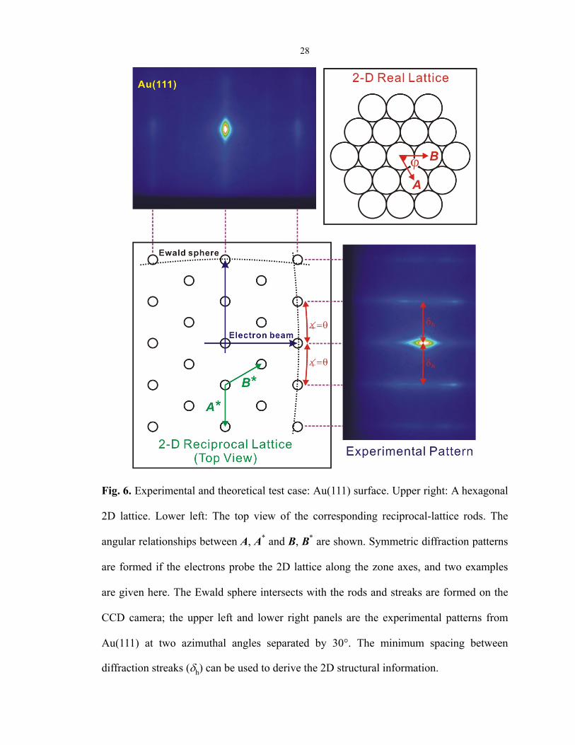
Fig. 6. Experimental and theoretical test case: Au(111) surface. Upper right: A hexagonal
2D lattice. Lower left: The top view of the corresponding reciprocal-lattice rods. The
angular relationships between A, A* and B, B* are shown. Symmetric diffraction patterns
are formed if the electrons probe the 2D lattice along the zone axes, and two examples
are given here. The Ewald sphere intersects with the rods and streaks are formed on the
CCD camera; the upper left and lower right panels are the experimental patterns from
Au(111) at two azimuthal angles separated by 30°. The minimum spacing between
diffraction streaks (h) can be used to derive the 2D structural information.

29
parallel to the specimen surface. In fact, there are 5 different Bravais lattices in 2D (real
space and reciprocal space) and for each, the characteristic is different; diffraction
patterns repeat their appearance every 60° for hexagonal, 90° for square, 180° for
rectangular and centered rectangular, and 360° for oblique lattices. Further verification
for a certain 2D lattice can be obtained by examining the azimuthal separation between
different symmetric patterns (see below). In the case of Au(111), another symmetric
pattern can be observed by 30° rotation (Fig. 5, lower right).
Geometrically, two vectors, A and B perpendicular to the n̂ , form the basis of the
2D lattice in real space [see Fig. 6, upper right panel for Au(111)]. The corresponding
reciprocal lattice, given by Fourier transformation, is an array of rods extended along n̂
with two basis vectors defined by
A* = 2(B× n̂ )/|A×B| and B* = 2( n̂ ×A)/|A×B|. (17)
Thus, |A*| = 2/|A|sin and |B*| = 2/|B|sin, (18)
where is the angle between A and B (see also Fig. 1, middle). Because of these direct
relationships between A and A* (B and B*), the azimuthal rotation in real space allow us
to probe different zone axes of the reciprocal lattice for the observation of symmetric
diffraction patterns (Fig. 6, lower left).
For the case of the electron beam propagating along a direction for which the
ZOLZ is parallel to A*, the minimum horizontal s will be equal to |A*| (Laue condition)
according to Ewald construction. Therefore, the total angle of deflection
= tan–1(h/L) = 2sin–1(s/4) = 2sin–1( / 2|A|sin),
L = h/tan[2 sin–1( / 2|A|sin)], (19)
where h is the horizontal spacing between spots (rods) and L is the camera length from
the scattering position to the camera. By the azimuthal rotation, which yields other

30
symmetric diffraction patterns, the value of that depends on the surface crystal structure
can be determined. If L is determined independently, the lattice constants |A| and |B| can
be obtained with the use of Eq. 19, and the 2D structure is thus determined.
For Au(111), the diffraction patterns taken at two zone axes (Fig. 6, upper left and
lower right) correspond well with a hexagonal reciprocal lattice in 2D (Fig. 6, lower left).
Therefore, the 2D structure in real space is also a hexagonal lattice with |A| = |B|. The
smallest horizontal spacing between rods [(h)min] recorded with L = 17.0 cm (Fig. 6,
lower right) was 106 pixels (1 pixel = 44.94 m in our system), which gave the
experimental value of |A| to be 2.88(5) Å, totally consistent with the literature x-ray value.
Through 30° rotation, another zone axis was probed, and the measured spacing between
adjacent rods increased and became 1.73 times (h)min (Fig. 6, upper left), which was
expected (√3 fold) according to the 2D structure.
Conversely, the camera length L can be accurately determined using a crystal
lattice whose structure is known, and such an in situ measurement is free of any errors
due to, e.g., rotation of the crystal. A typical error in L is ~0.2%, which mostly originates
from the spatial width and jitter of the electron pulses. However, for a given experimental
setting during the time-dependent measurements, it is not the absolute values but the
relative changes that are most crucial for deciphering the structural dynamics involved,
and the accuracy in the determination of transient changes can be much higher (see, e.g.,
Chs. 4 and 5).
The third dimension, besides the surface two, of the lattice can be accessed by
measurements of the rocking curve that is the change of diffraction spots with the angle
of incidence, i (≡ /2). This can be easily understood from the Bragg’s formulation for
the diffraction condition. For example, the diffraction patterns of Au(111) and Si(111)

31
Fig. 7. Diffraction patterns (in false color) of (a) Au(111) and (b) Si(111) recorded at
different incidence angles (i). Gold shows rod-like diffraction patterns because it has a
large atomic number and electrons can only penetrate top few layers. For silicon, other
features such as Kikuchi lines and bands may interfere with rocking-curve construction.
recorded at selected incidence angles are shown in Fig. 7. By determining the angle at
which successive orders appear (especially for large n, where there is less interference
from 2D, other features and the refraction effect), we can obtain the vertical interplanar
distance, the spacing normal to the surface. From Bragg’s equation (Eq. 11), the
measured change in i for two consecutive orders is given, for small i, by
i ≡ (/2) ~ sin(i + i) – sini = / 2d. (20)
For consistency, d can also be obtained from the vertical separation between two
consecutive spots v (≡ s) and with the use of the value of L, since
v ≈ L [tan(/2 + ) – tan(/2)] ~ L = 2L (/2) ~ L / d. (21)
Low-order Bragg spots are not used because they are affected by the refraction effect (see
below), by the surface potential, morphology and quality, and of course by the presence
of adsorbates. Construction of the rocking curves for the (111) surface of gold and also

32
Fig
. 8.
Obs
erve
d ro
ckin
g cu
rves
for
the
(11
1) s
urfa
ce o
f go
ld
and
sili
con.
R
ocki
ng
curv
es
are
obta
ined
by
re
cord
ing
diff
ract
ion
patt
erns
at
di
ffer
ent
inci
denc
e an
gles
. A
s th
e
inci
denc
e an
gle
is
grad
uall
y in
crea
sed,
ac
cord
ing
to
Ew
ald
cons
truc
tion
, Bra
gg s
pots
wil
l ap
pear
in-
phas
e an
d ou
t-of
-pha
se
alte
rnat
ivel
y. A
nar
row
ver
tica
l st
rip
alon
g a
stre
ak i
s av
erag
ed
hori
zont
ally
for
eac
h im
age,
res
ulti
ng in
a 1
D in
tens
ity
curv
e fo
r
each
inci
denc
e an
gle.
The
se c
urve
s ar
e th
en c
ombi
ned
into
a 3
D
figu
re, i
.e.,
inte
nsit
y be
ing
plot
ted
as a
fun
ctio
n of
the
inc
iden
ce
angl
e an
d ve
rtic
al p
ixel
num
ber
(a m
easu
re o
f s)
. A
t la
rge
inci
denc
e an
gles
, th
e B
ragg
spo
ts a
ppea
r w
ith
regu
lari
ty a
nd,
from
bot
h th
e ve
rtic
al s
paci
ng ( v
) an
d th
e ch
ange
of
inci
denc
e
angl
e ( i
) be
twee
n tw
o co
nsec
utiv
e di
ffra
ctio
n or
ders
, th
e
inte
rpla
nar
dist
ance
d c
an b
e ob
tain
ed.
The
ind
icat
ed s
hado
w
edge
is th
e ou
tgoi
ng e
lect
ron
scat
teri
ng p
aral
lel t
o th
e su
rfac
e.
32

33
Fig. 9. Indexed diffraction patterns of (a) Au(111) and (b) Si(111). Indices for
higher-order Bragg diffractions on the central streak are determined by using the Bragg
condition (Eq. 21). Indices for streaks are assigned according to the 2D lattice of the
surface plane. Diffractions from the first-order Laue zone (FOLZ) may be out of the
camera region if the electron incidence angle is large.
that of silicon is illustrated in Fig. 8. Clearly, high-order Bragg spots appear with
regularity, and we obtained dAu(111) = 2.36 Å and dSi(111) = 3.15 Å by using Eq. 21. These
values are consistent with the x-ray literature values of the crystals.
Therefore, given the geometry of probing in RHEED, the central streak in the
diffraction pattern contains the information about the interplanar distance along the
surface normal; the evolution of the horizontal spacing between streaks with the
azimuthal angle defines the symmetry of the 2D lattice in the surface plane, and gives the
corresponding lattice constants. Although the RHEED technique is not intended for
solving unknown crystal structures, it is designed to be used for the structural analysis of
exposed crystal surfaces. In Fig. 9, two indexed patterns are shown as examples.
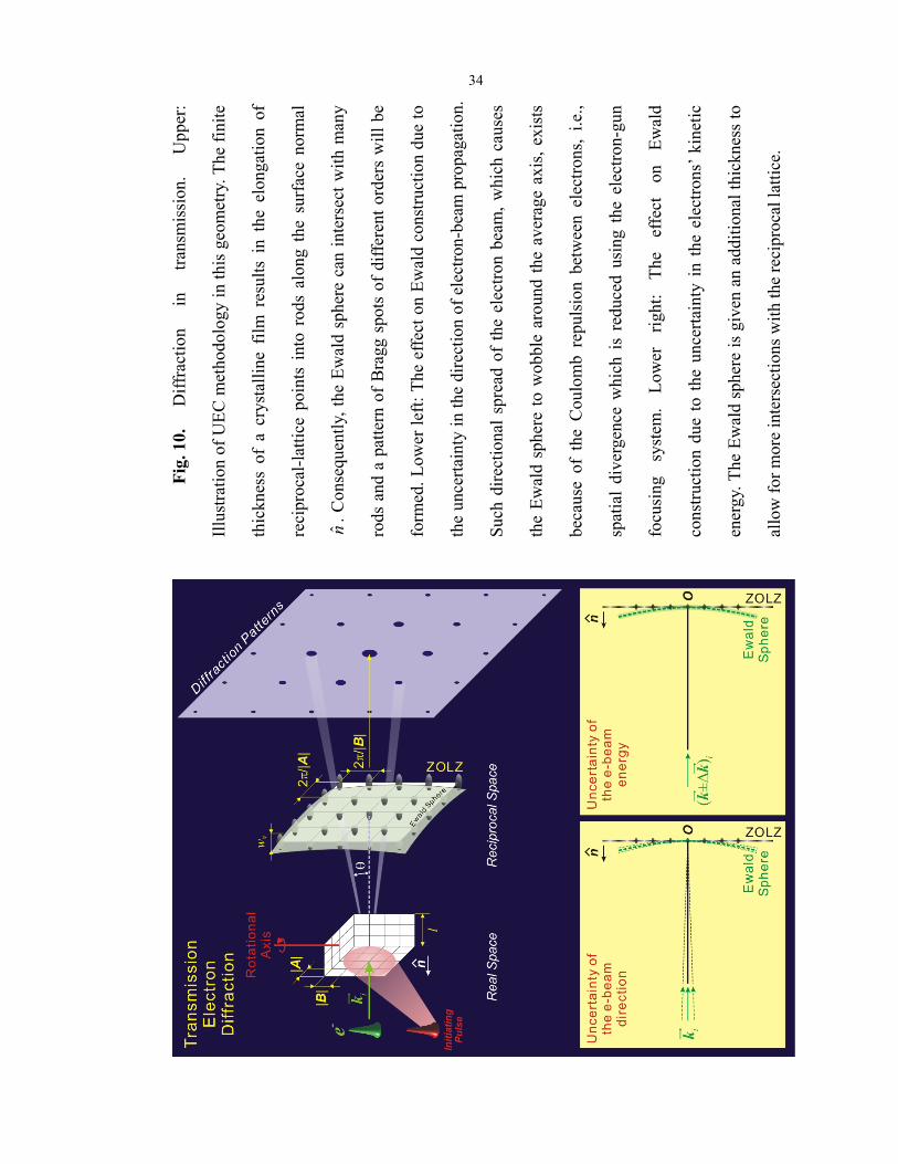
34
Fig
. 10.
D
iffr
acti
on
in
tran
smis
sion
. U
pper
:
Illu
stra
tion
of
UE
C m
etho
dolo
gy in
this
geo
met
ry. T
he f
init
e
thic
knes
s of
a c
ryst
alli
ne f
ilm
res
ults
in
the
elon
gati
on o
f
reci
proc
al-l
atti
ce p
oint
s in
to r
ods
alon
g th
e su
rfac
e no
rmal
n̂.
Con
sequ
entl
y, t
he E
wal
d sp
here
can
int
erse
ct w
ith
man
y
rods
and
a p
atte
rn o
f B
ragg
spo
ts o
f di
ffer
ent
orde
rs w
ill
be
form
ed. L
ower
lef
t: T
he e
ffec
t on
Ew
ald
cons
truc
tion
due
to
the
unce
rtai
nty
in th
e di
rect
ion
of e
lect
ron-
beam
pro
paga
tion
.
Suc
h di
rect
iona
l sp
read
of
the
elec
tron
bea
m,
whi
ch c
ause
s
the
Ew
ald
sphe
re t
o w
obbl
e ar
ound
the
ave
rage
axi
s, e
xist
s
beca
use
of t
he C
oulo
mb
repu
lsio
n be
twee
n el
ectr
ons,
i.e
.,
spat
ial
dive
rgen
ce w
hich
is
redu
ced
usin
g th
e el
ectr
on-g
un
focu
sing
sy
stem
. L
ower
ri
ght:
T
he
effe
ct
on
Ew
ald
cons
truc
tion
due
to
the
unce
rtai
nty
in t
he e
lect
rons
’ ki
neti
c
ener
gy. T
he E
wal
d sp
here
is
give
n an
add
itio
nal
thic
knes
s to
allo
w f
or m
ore
inte
rsec
tion
s w
ith
the
reci
proc
al la
ttic
e.
34

35
For a polycrystalline sample, namely, a sample consisting of many small
crystallites randomly oriented in space, a diffraction pattern will show the
Debye–Scherrer rings instead of spots. It is because the effective reciprocal lattice
becomes a series of concentric spheres centered at the reciprocal space origin (a
consequence of the random orientation in real space) and their intersections with the
Ewald sphere give rise to rings. From the radial average, a 1D diffraction curve can be
obtained; care must be taken and a fitting procedure is often necessary for the
determination of the center, because a large part of the rings below the shadow edge is
blocked. The peak positions correspond to the values of the reciprocal lattice vectors
( hklG
) for different planes indexed by the Miller indices, (hkl). The structure of the
crystallites can be obtained by comparing the experimental data with the simulated
diffraction curves for different crystal structures, as has been demonstrated in the UEC
study of interfacial water (9).
A.3. Diffraction in Transmission
In contrast to the reflection mode, the diffraction patterns of crystalline thin films
in transmission show many spots of different planes and orders. This is because of several
reasons. First, due to the 2D-like thickness of the film in the n̂ direction, reciprocal
lattice points are elongated into rods along n̂ , as mentioned previously. Figure 10
illustrates an example in which the electrons are propagating parallel to n̂ . According to
Ewald construction, the origin of the reciprocal space (000) is on the Ewald sphere, and
the ZOLZ plane is tangent to the sphere. If the reciprocal lattice consists of points only,
no other spots [except the (000)] on the ZOLZ will be in contact with the sphere due to
the sphere’s curvature. However, because the reciprocal points are elongated (finite 2D
thickness), the tips of the rods may intersect with the Ewald sphere so that more Bragg

36
spots appear in the diffraction pattern.
Second, when a macroscopic area is probed, the slight uncertainty of the crystal
orientation across the thin film due to its unevenness will introduce a small angular span
in the reciprocal lattice so that it has more chance to intersect with the Ewald sphere.
Third, the finite spatial convergence/divergence of the electron beam provides an
uncertainty of the direction of ik
, which results in a solid cone around the average axis.
Therefore, Ewald construction indicates that the sphere wobbles around that principal
axis and sweeps a larger region in k space, allowing for more intersections (Fig. 10, lower
left). Finally, the kinetic energy span of electrons, which causes the uncertainty of | ik
|,
gives the Ewald sphere an additional thickness to occupy a larger volume in k space.
Hence, its intersection with reciprocal rods becomes more likely (Fig. 10, lower right).
Due to the aforementioned reasons, one can see that, in order to record more
intense non-center Bragg spots, the crystalline film needs to be slightly rotated away from
the original zone axis in order to optimize the overlap between the reciprocal rods and
Ewald sphere. However, too much rotation can move the rods entirely away and result in
no intersection. The span of rods in reciprocal space can be estimated from the rocking
curves acquired through rotation of the crystalline film (along the vertical direction in
Fig. 10) to change the incidence angle of the probing electrons, similar to the
measurement of rocking curves in reflection experiments. The vertical width of rods (wv)
can be obtained from knowledge of the intensity angular profile of spots (hkl) because
wv ≈ G hkl (22)
where G is the perpendicular component of Ghkl with respect to the rotational axis. We
can also estimate the specimen thickness l over which diffraction is effective from the

37
Fig. 11. Ewald construction in k space for electron and x-ray diffraction. The typical
wavelength of high-energy electrons is much shorter than that of x-ray used for structure
analysis, which leads to a much larger Ewald sphere for electrons (dashed arc) than that
for x-ray (solid circle). The small-angle approximation can be used in the geometrical
theory for electron crystallography and facilitate the visualization of the Laue condition.
Scherrer formula (7)
l ≈ K/[hkl·cos(/2)] = K·2/wv (23)
where K (close to 1) is the shape factor of the average crystallite.
The structure of the 2D crystal is revealed in a single transmission diffraction
pattern without rotation. From knowledge of the camera length and by Eq. 19, it is
straightforward to obtain the lattice parameters. Of course, if the structure of the crystal
under investigation is more complicated than that of a very thin, simple specimen
consisting of light elements, one has to consider the issue of intensity, which may
O

38
additionally involve dynamical scatterings, but generally the determination of the orders
of Bragg spots (lattice symmetry) can be obtained. As for a polycrystalline sample,
similar procedures, as those discussed in the previous subsection, are used for structural
determination.
A.4. Advantages and Selected Topics of Electron Diffraction
Throughout the previous description of the geometrical theory for electron
diffraction, the small-angle approximation, sin ~ tan ~ , was often made. As
mentioned earlier, its validity comes from the order-of-magnitude difference between
and d in Eq. 11. Furthermore, the corresponding Ewald sphere relative to the reciprocal
lattice in k space has a large radius and, consequently, may be approximated as a plane.
Therefore, visualization of the Laue condition through Ewald construction becomes a
simpler task for high-energy electron diffraction, and fast calculations can be carried out
to extract the lattice constants from recorded diffraction patterns. This also becomes an
advantage for dynamics studies when correlating the observed diffraction changes as a
function of time with actual transient modifications in the structures (which will be made
clear from the discussion in the next section). In comparison, the typical wavelength of
x-ray used for structure analysis is much longer, and the size of the corresponding Ewald
sphere is, in fact, comparable to the reciprocal lattice vectors. It is easy to see from
Fig. 11 that the Laue condition in Ewald construction for x-ray diffraction is less visual
and involves more calculations than those presented above for electron diffraction.
Reducing the x-ray wavelength is much more difficult compared to the case of electrons,
which is readily attainable by increasing the acceleration voltage.
A.4.1 Surface Morphology and RHEED Pattern
The strong electron–matter interaction offers great opportunities for the studies of

39
Fig
. 12.
Sch
emat
ics
for
the
corr
elat
ion
of (
a) s
ampl
e cr
ysta
llin
ity
and
(b)
surf
ace
mor
phol
ogy
wit
h th
e ob
serv
ed d
iffr
acti
on p
atte
rn.
Sam
ple
cond
itio
ns t
hat
prod
uce
idea
l R
HE
ED
and
tra
nsm
issi
on p
atte
rns
are
give
n in
the
upp
er p
anel
s. E
ven
in r
efle
ctio
n ge
omet
ry,
any
type
of
elec
tron
pen
etra
tion
res
ults
in a
tran
smis
sion
-lik
e pa
tter
n (p
anel
a, b
otto
m, a
nd p
anel
b, m
iddl
e). I
ncre
ase
of th
e sp
ot w
idth
is a
long
the
dire
ctio
n of
the
crys
tall
ites
’ red
uced
dim
ensi
on, a
cor
rela
tion
dic
tate
d by
the
prin
cipl
e of
Fou
rier
tran
sfor
mat
ion.
39

40
nanometer-scale structures and interfacial phenomena that are less straightforward for
x-ray because of its large penetration depth and weak interaction with specimens in
general. The same characteristic, however, also makes RHEED sensitive to the surface
morphology of the specimen, whose studies in the fields of thin film growth and surface
structure determination are actually the main application of this technique (6, 10, 11).
From the types of diffraction patterns observed, the samples’ crystallinity and surface
morphology may be deduced, as illustrated in Fig. 12 (10). In principle, studies of
structural dynamics can be made for all these cases as long as the diffraction spots or
rings are distinct and well-defined; in practice, a sample surface that is close to
atomically flat (at least within a certain 2D range) is more desirable because rough
surface morphology often leads to decrease of diffraction intensity, increase of diffuse
scattering background, and broadening of diffraction width that may hinder a proper
analysis of temporal changes. Sometimes, well-oriented small crystallites that give a
transmission-type pattern may be more beneficial to dynamics studies because of the
cross reference obtained from different spots (see Chs. 6 and 7). The stringent
requirement of atomically flat surfaces for studies is hence not always necessary.
A.4.2 Electron Mean Free Path and Penetration Depth
It is essential to estimate the electron penetration depth ( e ) at a given electron
wavelength in a medium. This can be achieved by knowing the mean free path ( e ) for
elastic scattering from the total cross section of scattering () and the density of scatterers
(N), with the use of the following equations:
N1
e and the differential cross section 2
d
dsf
(24)
where denotes the solid angle. With Eq. 5 and the angular integration of d/d, a
screened-potential model that effectively describes the atomic potential for neutral

41
Table 1: Mean free paths and penetration depths for elastic scattering of electrons.
substance Z N (Å-3) e (Å) at 30 kV e (Å) at 30 kV
graphite 6 2/(2.462·6.70 sin60°) 2750 192 at i = 4°
silicon 14 8/5.433 1010 70 at i = 4°
35 at i = 2°
interfacial water
(cubic form)
8 for O
1 for H
8/6.3583 for O
16/6.3583 for H 3050 53 at i = 1°
(transmission-like)
gallium arsenide 31 for Ga
33 for As
4/5.653
for Ga and As 380 20 at i = 3°
vanadium dioxide
(monoclinic) 23 for V
8 for O
4/118 for V
8/118 for O 520 45 at i = 5°
zinc oxide 30 for Zn
8 for O
2/(3.252·5.20 sin60°)
for Zn and O 370 20 at i = 3°
elements in relation to the atomic number (Z) and a screening radius gives a good
approximation for , especially when the scattering angle is not too small (11). The final
result is
34212.0 Z . (25)
The estimated mean free paths for elastic scattering and the corresponding penetration
depths (at typical probing conditions) for several substances are given below in Table 1;
their differences should be noted because, without the consideration of refraction,
iee sin (for single elastic scattering). (26)
The simple estimation presented above shows that, with the criterion of energy-
and momentum-conserved single scattering, electrons probe mostly the surface region of
a specimen but do penetrate several unit cells (interplanar distances). The latter property
is important in that UEC studies are still capable of resolving bulk-related structural
dynamics, with a surface sensitivity. It should be noted that the values of penetration

42
Fig. 13. Tangential continuity at the surface where the wave fronts are refracted.
Medium II attracts electrons more than medium I, and the dashed line indicates the
surface normal.
depth in Table 1 may be underestimated. If the surface morphology is less perfect than an
atomically flat one, or more than one scattering event occurs so to contribute some
diffraction intensities, electrons can reach a deeper region into the bulk. When a material
contains much heavier elements (e.g., gold), the observed electron diffraction is expected
to originate solely from the top layer and form streaks; an example can be seen in Fig. 5.
A.4.3 Inner Potential and Electron Refraction
The phenomenon of electron refraction occurs when the probing particles pass
through the interface between vacuum and the specimen or between different materials.
This phenomenon exists because electrons experience the difference of the electrostatic
potential in different media. Compared to the vacuum environment, the superposition of
the atomic potentials in a real material attracts and hence slightly accelerates an electron,

43
which leads to a small change in the wavevector. In an average sense without going into
the structural details of atomic arrangement, the mean value of the crystal potential is
called the inner potential, VI (in volts), typically a positive number for attraction. In
Fig. 13, medium II has a higher VI than medium I, causing the traveling electrons to bend
toward the surface normal.
Because the discontinuity of VI appears at the interface along the surface normal,
the wavevector change should only occur in that direction. Thus, for a featureless
interface, tangential continuity of the wave fronts is required, yielding an analogue of
Snell’s law in optics (11):
2
2
1
1 sinsin
(27)
where 1 (2) is the incident (refractive) angle with respect to the surface normal and 1
(2) is the wavelength in medium I (II) (Fig. 13). With the use of Eq. 3, the relative
refractivity can be written as
0
I1I2
I106
I10
I206
I20
2
112
21
109785.01
109785.01
sin
sin
V
VV
VVVV
VVVVn
. (28)
The approximation is justified because the inner potentials VI1 and VI2 are generally much
smaller than the acceleration voltage used. Furthermore, the small-angle approximation
valid for typical RHEED experiments gives
0
I1I2
2
2
2
12i 2
π
2
π
V
VV
. (29)
As an example, for Si(111) with VI ~ 11 eV, the Bragg angles given by Eq. 11 (without
taking into account the structure factor) are /2 – 2 ≈ n/2dSi(111) = 11n mrad for 30-keV
electrons; the corresponding i’s for the first 8 orders are nonexistent, 11.4, 27.4, 40.2,
52.3, 64.0, 75.5, and 87.0 mrad, respectively. It is now clear why the regularity of Bragg

44
condition is restored for higher-order spots (n ≥ 5) in the rocking curve shown in Fig. 8,
lower right panel. The reflection of electrons by an atomically flat surface may be the
major scattering events at very small incidence angles, which forms the specular spot that
has little diffraction contribution for these probing conditions. As a result, UEC studies
should be conducted with care with this phenomenon in mind.
A.4.4 Coherence of the Electron Beam
For electromagnetic waves, photons that are generated from a coherent source
such as a monochromatic laser can propagate parallel and keep their phase because of
their noninteracting nature; the plane-wave description by Eq. 1 is therefore appropriate.
Such a model for the wave property of electrons has its limit in reality due to the
following reasons. As mentioned earlier, any factor that causes the deviation of ik
will
lead to small changes in diffraction condition. Unlike photons, the Coulomb force causes
electrons to interact with one another. As a result, collisions and the space-charge effect
exist and destroy the coherence of charged particles, especially for a high-density beam.
This issue may be reduced by lowering the number of electrons in a spatiotemporal bunch
or totally eliminated by using single-electron packets (12).
However, real electron sources inevitably have finite sizes and energy spread that
result in a finite angular spread () and the spread of the wavenumber (k). The
effective coherence length () is a distance between two points from which the wave
packet is scattered with a 180° phase difference (and hence no coherence) (11). From k
and along the electron propagating direction,
0
6
06
02
Δ||, 109785.021Δ
109785.0152.24
ΔΔ
π2
VV
VV
kk
(in Å), (30)
with the use of Eq. 3 and the assumption of the potential spread V << V0. The value of

45
Fig
. 14.
Str
uctu
ral
mod
ific
atio
ns i
n th
e cr
ysta
l la
ttic
e an
d th
e co
rres
pond
ing
diff
ract
ion
chan
ges.
The
dif
frac
tion
dif
fere
nces
obs
erve
d
as a
fun
ctio
n of
tim
e by
UE
C a
re th
eref
ore
indi
cati
ve o
f th
e di
ffer
ent a
tom
ic m
otio
ns in
the
latt
ice
stru
ctur
e.
45

46
||, k ~ 41 nm is obtained for V = 10 V and V0 = 30 kV. From and perpendicular to
the beam direction,
, = 2/k =2/(k) = / (31)
and has a value of about 7–70 nm for a typical of 1–0.1 mrad. The angular spread also
results in a coherence length along the electron beam direction,
ΔsinΔ
π2
i||Δ||,
k (32)
because k|| = (k cosi) = k sini . For the aforementioned typical and at i = 3°,
||, is about 130–1300 nm. The estimation of the coherence length above signifies that
electrons generated by a real electron source can only “see” coherently a spatial range of
the nanometer to sub-micrometer scale.
B. Nonequilibrium Transient Structures
In time-resolved experiments, the main diffraction features for studies of
structural dynamics are the positions, intensities, widths, and the shapes of Bragg spots or
Debye–Scherrer rings. Background intensity and Kikuchi patterns may also evolve as a
function of time, but in general, their intensities and distributions are weak and diffuse. In
the following discussion, we will focus on transient changes of the main diffraction
features observed in UEC and make connections with x-ray studies (13-15). Summarizing
in Fig. 14, in general, the position shift of Bragg spots or rings is directly related to lattice
expansion or contraction; the change of the width and shape indicates the emergence of
dynamical inhomogeneity; and the intensity change is the result of incoherent thermal
motions, coherent lattice vibrations, or phase transitions.
B.1. Shifts of Diffraction Spots and Rings
Following an ultrafast excitation, diffraction spots or rings change their positions
vertically and/or horizontally to reflect the changes in interplanar distances. Such changes

47
Fig. 15. Temporal changes of diffraction spot position. The faded rods and curves
indicate the negative-time equilibrium configuration. As the real lattice expands along n̂
at positive times the reciprocal rods move downward, which leads to a downward
movement of Bragg spots.
need to be homogeneous (uniformity of distance change) over essentially the entire
spatially probed region, a requirement for preserving the Bragg condition. Thus, these
shifts provide the unequivocal evidence for the homogeneous lattice expansion or
contraction, depending on the direction of the shift.
We first consider the vertical lattice change along n̂ . According to the Laue
condition of Eq. 12, a small vertical shift of the Bragg spot on the center (00) rod,
(0A* 0B*), is directly related to the change in the vertical lattice spacing by the following
relationship:
s/s = –d/d = –(/2)/tan(/2) (33)
which becomes –/ when is small. Consequently, a decrease (increase) in s, i.e.,

48
when the Bragg spot shifts toward (away from) the direct beam position in the diffraction
pattern, is a measure of the increase (decrease) in d. In reciprocal space, such a lattice
change can be visualized as the rods moving parallel to n̂ and intersecting with the
Ewald sphere but maintaining their size or shape (Fig. 15). The same picture can be
applied to the description of movements in the horizontal direction.
On the ultrashort time scale, it is critical to understand the dynamics responsible
for a downward shift, which is the observation made in many UEC studies. The first
mechanism that comes to mind involves conventional heating, due to the anharmonicity
of the lattice. The 1D thermal expansion is usually expressed as x = (3g/4b2)kBT,
which is deduced from the anharmonic potential energy U(x) = bx2 – gx3 – fx4 with
positive b, g, and f (16). However, at room temperature, the (linear) thermal expansion
coefficient (l) for most of the crystalline solids is on the order of 10–5 to 10–6 K–1; for
example, l×106 = 2.6, 5.73 and 14.2 for silicon, gallium arsenide and gold, respectively.
Thus, a maximum thermally driven change of 1% in lattice spacing requires a lattice
temperature jump of about 3850, 1750 and 700 K, which are not reachable at our
excitation fluences and in a very short time. To achieve a temperature jump (Tl) at the
surface, the fluence for heating required is given by
Fheating/ = (Flaser/)(1 – R)(Eexcess/Ephoton) ~ ClTl , (34)
where is the penetration depth (inverse of the absorption coefficient, 1/) of the light
(photon energy Ephoton) with fluence Flaser; R is the reflectivity, Eexcess is the above-gap
excess energy, and Cl is the heat capacity of the lattice. For gallium arsenide, for example,
Cl = 1.74 J/cm3K, the band gap Eg = 1.423 eV, R ~ 0.3 (0.45) and ~ 710 (6.4) nm for
800 (266) nm normal-incident light (17). A fluence of Flaser = 10 (1) mJ/cm2 at
800 (266) nm gives the value of Tl to be 4.6 K at 800 nm or 340 K at 266 nm.

49
Experimentally, this is in contradiction with the large observed shift. More importantly, as
will be shown in Ch. 4, the spot-shifting behavior for the 800- and 266-nm excitations are
contrary to the trend obtained above.
It follows that on the ultrashort time scale, the nonequilibrium state of the lattice
must be considered. In this state, only certain types of the atomic motions may be initially
launched, and the assumption of thermal equilibrium for all modes is not valid.
Furthermore, carrier excitation can affect the lattice potential, resulting in a new state of
weaker chemical bonding and hence a different structure. This expansion by a
“potential-driven,” carrier-assisted mechanism does not depend on lattice temperature but
on the carrier density. When the number of carriers decreases (through diffusion, for
example), the expansion would decrease and the system recovers accordingly. Finally, the
expansion in the vertical and horizontal directions may show anisotropy in the temporal
behavior with different amplitudes for the change. Manifestation of these features of
nonequilibrium behaviors can be seen in the studies made on GaAs (Ch. 4).
B.2. Changes of Widths and Shapes
The widths and shapes of Bragg spots or rings in a diffraction pattern are affected
by the crystal size (Eq. 23), inhomogeneity and embedded strain in the sample, by
electron refraction due to the shape of the crystallites (Sec. A.4.1), and by the uncertainty
of the direction and magnitude of the probing electrons’ momentum ik
(size of the
electron beam). However, their transient differences from a static reference can only stem
from the structural changes induced by the optical excitation. In the case of
polycrystalline samples, the average size of the crystallites may change (e.g., during
ultrafast melting or annealing), resulting in the broadening or narrowing of diffraction
rings according to the Scherrer formula (Eq. 23). The shape may also develop to a

50
Fig. 16. Temporal changes of diffraction width. The faded rods and curves indicate the
negative-time equilibrium configuration. Lattice inhomogeneity (along n̂ ) generated in
the crystal makes the reciprocal rods elongated, and their intersections with the Ewald
sphere give a diffraction pattern with larger vertical width.
Gaussian-like function, which reflects an increased inhomogeneity. In the case of
crystalline samples, however, this spatial size change is not of concern since the crystal
essentially preserves its order. Thus, in this case, lattice inhomogeneity is due to a small
modification of the average lattice spacing or a strain of propagating acoustic waves
following the excitation.
Following the above discussion of the reciprocal-space picture, it is clear that, if
the lattice planes evolve to two distributions of distances around d, one larger and one
smaller, then this strain propagation will result in two side bands (or broadening) in k
space around the central value (see Fig. 16). Such behavior is commonly caused by an
acoustic sound wave of relatively small wavelength. Coherent acoustic motions are

51
typically generated through carrier excitation or from the decay of another type of
initially generated lattice vibration, e.g., optical phonons. In an elementary metal,
acoustic phonons are directly generated following carrier generation because only one
atom exists in the primitive unit cell and there is no optical branch. However, in a
semiconductor with more than one atom in the primitive unit cell, optical phonons are
present and become the doorway for efficient coupling with the carriers. These optical
phonons have a lifetime during which they convert to acoustic ones, and the latter into
thermal motions on a time scale determined by the anharmonicity of the lattice.
The inhomogeneity of the lattice generated parallel to the sample surface, i.e., the
horizontal broadening of reciprocal-lattice rods, has a more complicated effect: when
intersecting with the Ewald sphere, the rod projects not only a larger horizontal width but
also an enlarged vertical width in a diffraction pattern. However, the geometry of RHEED
allows the contributions to horizontal and vertical widths due to the dynamical
inhomogeneity of the lattice along different directions to be distinguished (see
Appendix B for the derivation). By monitoring the temporal evolution of spot widths in
the directions orthogonal to n̂ , lattice dynamics along the surface can be followed as a
function of time. The difference between the temporal evolution along the vertical and
horizontal directions in the diffraction patterns can provide information of such
anisotropy. As will be shown in Ch. 4, a key cause of the anisotropy is free movement
along the n̂ direction (surface vertical vs bulk lateral) and the change in lattice
potential.
B.3. Changes of Diffraction Intensities
On the basis of Eq. 9, the diffraction intensity of a Bragg spot (hkl) is proportional
to the square of the geometrical structure factor F(hkl), which is given by (5)

52
j
jjjjjhklj
j zlykxhifrGifhklF π2expexp)(
(35)
where fj is the atomic scattering factor of the jth atom in a primitive unit cell. Since the
determination of F(hkl) involves the positions of atoms, jr
≡ (xj, yj, zj), in a unit cell, any
lattice motions that appreciably change their relative positions can cause the diffraction
intensity to change. These motions are those of optical phonons (see, e.g., Refs. 13–15
and 18), small-wavelength acoustic phonons, and the thermal motions. In contrast,
homogeneous lattice expansion or contraction has no influence on the intensity of the
Bragg spots. The contribution of the thermal, incoherent motion (in all directions) in
diffraction intensities can be calculated using the DW expression, Eq. 16.
The ability in UEC to resolve the diffraction in time and for different Bragg spots
makes possible the separation of contribution by these different processes, especially that
horizontal and vertical lattice motions manifest themselves differently. The change of
spot intensity on the (00) rod will display vertical motions, whereas those on the side will
have contributions from both vertical and horizontal motions. However, incoherent
thermal motion affects all of the Bragg spots. For the case of gallium arsenide as an
example, this separation is clear. The crystal has a face-centered-cubic lattice with a
two-atom basis that has gallium at Gar
≡ (0, 0, 0) and arsenide at Asr
≡ (1/4, 1/4, 1/4) in
the unit cell in the equilibrium state. If, say, n̂ is [001], the intensity of the Bragg spot
(0 0 4n) on the (00) rod is proportional to
|F(0 0 4n)|2 = |fGaexp(–8nizGa) + fAsexp(–8nizAs)|2. (36)
Thus, those optical phonons that have the Ga and As atoms vibrate against each other
along the vertical direction (e.g., longitudinal optical phonons) will affect the structure
factor and consequently the diffraction intensity. Horizontal vibrational motions, however,

53
have no influence because their projection on the vertical scattering vector is zero. On the
other hand, if thermal motion is responsible for the intensity reduction, Equation 16
provides the theoretical description. By monitoring the extent and time scale of the
intensity reduction for different Bragg spots, the lattice motions responsible for the
observed changes can be distinguished.
B.4. Transient Changes in Transmission Diffraction
Because of the probing geometry in the transmission mode, transient diffraction
patterns of crystalline thin films can directly provide the dynamic information in the 2D
structure. Due to the intersection between rods and the Ewald sphere, as shown in Fig. 10,
2D lattice expansion/contraction deduced from decrease/increase of the distances
between diffraction spots, or changes of structural homogeneity indicated by the width
changes, can be observed experimentally. Transient structural information along the n̂
direction could be masked, given the experimental geometry where the electron beam
propagation is essentially in the same direction of rods (see Sec. A.3 for discussion).
Naturally, if there is substantial lattice expansion along n̂ on the picosecond time scale,
such change can be observed in the reflection geometry. In transmission, however, this
n̂ -direction lattice motion can lead to intensity changes, as will be shown in Ch. 4.
Transmission electron diffraction has also been applied to studies of
polycrystalline metallic thin films by several groups, e.g., those of Miller (19), Cao (20),
and, earlier, Mourou (21). The issues of nonthermal solid-to-liquid phase transition and
electronically driven lattice changes have been discussed. However, due to the
polycrystalline nature of the sample, transient lattice motions in a single crystallite and
those between randomly oriented crystallites may be strongly correlated, and this could
complicate the interpretation of structural dynamics. The transmission study reported in

54
Fig. 17. Extraction of the horizontal and vertical profiles of a Bragg spot. The narrow
strips (yellow for the vertical direction and red for the horizontal) are the regions over
which intensity averaging is performed. Profiles obtained from the green strips (vicinity
of the Bragg spot) may be used for background subtraction when necessary.
Ch. 4 was, to our knowledge, the first study of structural dynamics of a single-crystal
semiconductor by electron diffraction, which displays the motion of the entire lattice.
B.5. Extraction of Transient Diffraction Changes
To quantify the aforementioned diffraction changes at transient times, a fitting
procedure is invoked to obtain the intensity, position, width and line shape of a Bragg
spot or diffraction ring as a function of time. For typical UEC studies, the analysis can be
made in 1D by considering the vertical and horizontal directions separately. The first step
is to collect the 1D profiles of a certain diffraction feature at different times, by averaging
over a narrow strip across the diffraction vertically or horizontally (Fig. 17). The
important issue here is to achieve a higher ratio of the signal to the background and noise.
The profile obtained from a wider strip may be less noisy but with a lower peak due to

55
Fig. 18. Results of the fit. (a) A constant offset or linear function is included in the fit of
an intensity profile with a flat or low background. (b) A quadratic (or higher-order)
function is used for the background. The inset shows the result of the fit that considers a
pure Gaussian form for the signal; the small discrepancy is visible.
the background in the less intense part; the profile from a narrower strip contains more
contribution from the signal, but can be less smooth. Thus, a balanced choice may be a
strip that covers (approximately) the horizontal or vertical full width at half maximum.
For fitting, a pseudo-Voigt shape function, fpV(s), is used,
,1 GLpV sfsfIsf (37)
.2ln4expπ
2ln22
,2/
2/
π
1
2
0G
220
L
w
ss
wsf
wss
wsf
The integral of fL(s) or fG(s) over s is unity (normalized), and Eq. 37 is a simple sum of
the two functions instead of a convolution (Voigt shape). Here, I represents the (1D)
integrated intensity, s the scattering vector coordinate, s0 the peak position, w the
(common) full width at half maximum, and the Lorentzian contribution. Depending on
the surface quality and the electron incidence angle, the diffuse background may be low

56
and flat enough such that no subtraction prior to fitting is needed (Figs. 17 and 18a);
when the background is not negligible, either a subtraction by the profile obtained from
the vicinity of the diffraction feature is made first, or a polynomial (typically quadratic)
function is include in the fit (Fig. 18b).
Comparisons between the extracted diffraction features—I(t), s(t), w(t), and (t),
where t is the delay time between the electron and optical pulses—are subsequently made
to elucidate the structural dynamics and relaxation pathway in the specimen. Based on the
previous discussion in Secs. B.1 to B.3, the similarity or difference between these
time-dependent features can provide crucial information about the involvement of the
candidate (structure-related) physical processes, their synchrony or sequence in time, and
the characteristic time constants that govern the structural dynamics.
B.6. Issues of Electron Refraction and Scalability of Diffraction Change
Two issues about the dynamical changes in UEC are addressed. The first one is in
regard to the diffraction changes caused by the electron refraction effect. According to the
discussion in Sec. A.4.3, the two reasons are the possible slight tilting of the surface
normal and the change of the inner potential, both of which result from the optical
excitation and may lead to small change in the diffracted beam direction. However, it can
be shown from the order-of-magnitude analysis that electron refraction plays a minor role
in the diffraction changes discussed above, for typical UEC studies with moderate optical
excitation.
The tilting of n̂ comes from the different extent of lattice expansion as a result
of the gradient of the excitation pulse profile on the specimen. This effect may be much
reduced by using a sample size or making the probed area within the region of relatively
homogeneous excitation. Furthermore, with the total vertical expansion of the lattice on

57
the order of 1 to 10 Å over the length of the probed region along ik
(on the order of
1 mm), electron refraction may cause an angular change of 10–4 to 10–3 mrad, much less
than the uncertainty of ik
itself and consequently unimportant. The inner potential of
matters is on the order of 10 V, and its change induced by moderate excitation is expected
to be on the order of 1 V or less. Thus, from Eq. 29, the induced angular shift would be
on the order of 10–3.5 mrad and hence negligible. For intense excitation, the electron
refraction effect due to larger surface or bulk potential change may be observed (22);
however, care has to be taken in interpreting the relative shifts of diffraction features,
which is the next issue discussed below.
On the basis of Eq. 33, diffractions from the same set of crystal planes with
different orders (n) are expected to exhibit shifts in proportion to n during the structural
dynamics, with the same (normalized) temporal evolution for the movements. In addition,
the accompanying changes in their intensities, if exist, should be scalable according to
Eq. 16 or Eq. 35, and follow one temporal profile only. The presumption behind is that all
of these diffractions originate from spatially the same part of the probed specimen.
However, if, for some reason, this is not the case, the scalability of diffraction shifts may
not hold; an additional observation that often accompanies with this somewhat
counterintuitive phenomenon will be the different time constants for diffractions of
different orders.
It should be noted that a pattern of many spots similar to the cases shown in
Fig. 12, bottom of panel a and upper three of panel b, comes with a transmission nature.
Due to the different electron traveling directions for different diffractions, lower-order
spots may originate spatially from the higher part of a crystallite (to avoid the blocking of
diffracted electrons by adjacent crystallites or surface structures) and the highest-order

58
one is formed by diffracted electrons that penetrate deeper. The key governing factor here
is the mean free path discussed in Sec. A.4.2. Such a phenomenon will be further
discussed in Ch. 5 with a real case. Proportionality of diffraction shifts becomes true for
solely transmission-type experiments such as studies of polycrystalline samples
(electrons penetrating small crystallites and forming the diffractions), and an example can
be seen in Ch. 10. For scalability of intensity changes, see Ch. 4 for the transmission case
and Ch. 8 for the reflection case.
Appendix A. Conventions
In the diffraction theory, the incoming beam is described by Eq. 1. In this
convention, the wavenumber k = | ik
| = 2/, and for electrons, k = /v where v = is
the velocity and = /2 is the frequency; the momentum of the particle p = ħk = mv,
and the de Broglie relation = h/p which consistently equals to 2/k. Accordingly, when
k is used in this form, a constant factor of 2 appears in diffraction expressions of k, s and
others such as the reciprocal basis vectors in 3D (Eqs. 13 and 14), those for a 2D
reciprocal lattice (Eq. 16), and the last part of Eq. 23.
Crystallographers use a different convention to define the wavevector, k = –1. As
such the factor 2 disappears, and, for example, the important relations π2 mRs
and s = (4/)sin(/2) become simply mRs
and s = (2/)sin(/2). In such a way, it
is straightforward to invert s directly into real-space distances. The crystallography
convention is equivalent to rewriting Eq. 1 for tr ,0 with the phase factor being
trk
iπ2 , where the new ki is 1/. The important point is to keep track of the
self-consistency regarding the momentum as the conventional p = ħk, or p = hk with k

59
being clearly defined. Unfortunately, these definitions, with or without 2, are used in
different areas of diffraction. For example, in gas-phase diffraction, s is defined with 2
included; for most of the following chapters, this convention is used.
Similarly, the definition of the angle of incidence being or /2 requires a
convention. Considering to be the total diffraction angle (see Fig. 2a), the incidence
angle would be /2; if the incidence angle is , then the total scattering angle would be 2.
The definition of s follows.
Appendix B. Reciprocal‐space Broadening of Rods
The following simple estimation is made for the effect of horizontal broadening of
the rods in reciprocal space on the observed width of diffraction spots. For an ordered
structure in 2D, the reciprocal lattice is made of rods, and when modulated by the
spacings in the n̂ direction, each zone should be considered as a symmetric-top-like
shape with wh = wx, wy being different from wv = wz. Therefore,
(2x/wh)2 + (2y/wh)
2 + (2z/wv)2 = 1
where x and y are the directions (in reciprocal space) orthogonal to n̂ , z the direction
parallel to n̂ , and wh (wv) is the full horizontal (vertical) width. Locally, the Ewald
sphere with large radius (large ħki) will cut through the rods nearly as a tilted plane
(Fig. 16) defined by (0, 1, 0) and (sin, 0, cos), where is the angle between n̂ [i.e.,
(0, 0, 1)] and plane direction. As a result, the elliptical trace where the rod and the plane
intersect has a horizontal width wh but the vertical width becomes (tan2 /wh2 + 1/wv
2)–1/2.
If, due to horizontal inhomogeneity, wh becomes wh + wh, the change of the
vertical width will be
wh tan2 /[tan2 + (wh/wv)2]3/2,

60
which is much less than or on the same order of wh. This is because in the reflection
geometry of UEC, is small and wv and wh are not significantly different within an order
of magnitude. It is noted that wv and wh are determined by the inverse of the coherence
length (on the order of 10 nm or more) and also affected by the specimen morphology.
References:
1. B. K. Vaĭnshteĭn, Structure analysis by electron diffraction (Pergamon Press,
Oxford, 1964).
2. H. M. Seip, in Selected topics in structure chemistry, P. Andersen, O. Bastiansen, S.
Furberg, Eds. (Universitetsforlaget, Oslo, 1967), pp. 25-68.
3. J. C. Williamson, Ph.D. thesis, California Institute of Technology (1998).
4. Z. L. Wang, Elastic and inelastic scattering in electron diffraction and imaging
(Plenum Press, New York, 1995).
5. N. W. Ashcroft, N. D. Mermin, Solid state physics (Saunders College Publishing,
Fort Worth, TX, 1976), pp. 101-108.
6. Z. L. Wang, Reflection electron microscopy and spectroscopy for surface science
(Cambridge Univ. Press, Cambridge, 1996).
7. B. E. Warren, X-ray diffraction (Dover, New York, 1990), pp. 38, 253.
8. J. F. Vetelino, S. P. Gaur, S. S. Mitra, Phys. Rev. B 5, 2360 (1972).
9. C.-Y. Ruan, V. A. Lobastov, F. Vigliotti, S. Y. Chen, A. H. Zewail, Science 304, 80
(2004).
10. P. K. Larsen, P. J. Dobson, Eds., Reflection high-energy electron diffraction and
reflection electron imaging of surfaces (Plenum Press, New York, 1988).
11. A. Ichimiya, P. I. Cohen, Reflection high-energy electron diffraction (Cambridge

61
Univ. Press, Cambridge, 2004).
12. A. Gahlmann, S. T. Park, A. H. Zewail, Phys. Chem. Chem. Phys. 10, 2894 (2008).
13. A. Rousse, C. Rischel, J.-C. Gauthier, Rev. Mod. Phys. 73, 17 (2001).
14. C. Bressler, M. Chergui, Chem. Rev. 104, 1781 (2004).
15. M. Bargheer, N. Zhavoronkov, M. Woerner, T. Elsaesser, Chemphyschem 7, 783
(2006).
16. C. Kittel, Introduction to solid state physics (John Wiley & Sons, Inc., New York,
7th ed., 1996), pp. 129-131.
17. S. Adachi, Optical constants of crystalline and amorphous semiconductors:
Numerical data and graphical information (Kluwer Academic Publishers, Boston,
1999), pp. 221, 225.
18. K. Sokolowski-Tinten et al., Nature 422, 287 (2003).
19. B. J. Siwick, J. R. Dwyer, R. E. Jordan, R. J. D. Miller, Chem. Phys. 299, 285
(2004).
20. S. H. Nie, X. Wang, H. Park, R. Clinite, J. M. Cao, Phys. Rev. Lett. 96, 025901
(2006).
21. S. Williamson, G. Mourou, J. C. M. Li, Phys. Rev. Lett. 52, 2364 (1984).
22. R. K. Raman et al., Phys. Rev. Lett. 101, 077401 (2008).