chapter 3. diaphragm-base pressure sensor fabrication
TRANSCRIPT

Chapter 3. Diaphragm-base Pressure Sensor Fabrication
35
Chapter 3 Diaphragm-based Pressure Sensor Fabrication
Because the sensor is intended to operate under harsh environment such as high
temperature and high pressure, therefore using materials with very the same CTE
(coefficient of thermal expansion) as that of optical fiber is very important to reduce
thermal induced air-gap changes and failures. Ordinary single mode optical fibers are
made of fused silica. It’s very straightforward to use fused silica for the ferrule and the
diaphragm. Also fused silica can be micro-structurable, preferably using standard
lithography process (batch fabrication).
However, all fused silica doesn’t mean that the fabrication of a diaphragm-based EFPI
sensor is simple. Actually, fused silica wafers or ferrules are hard to polish, and difficult
to bond together, especially at low temperature. Therefore, some special techniques are
investigated to fabricate sensors with fused silica wafers and ferrules.
3.1 Diaphragm-based EFPI Pressure Sensor Fabrication Process The process of the sensor fabrication includes:
1) photolithography on fused silica diaphragms;
2) polishing fused silica ferrule end;
3) bonding the diaphragm and the ferrule;
4) and bonding the ferrule and the fiber.
The pressure sensor consists of a thin diaphragm, which deforms in response to a change
in pressure. The diaphragms have been micro-machined in order to form cavities. In our
experiments, the cavities are etched round, 0.5mm radius. By using deep wet etching
technology, 20 or 30 micron-deep pits can be obtained in 5 hours.
The fused silica ferrule end is polished to enhance the bonding quality with the
diaphragm. The surface roughness on the ferrule can cause voids or even much larger
un-bonded areas.
Chapter 3. Diaphragm-base Pressure Sensor Fabrication
36
Bonding is usually one of the most critical issues in sensor fabrication. The bonding
method will finally affect the performances of the sensor and will determine the
temperature dependence directly. Though there are a lot of bonding methods available,
fused silica and fused silica bonding, which also need to be at low temperature, still
remains a good topic for further investigation. There are also other challenges imposed
by the small size of the sensor, such as fine optical alignment and diaphragm cutting.
We chose the intermediate-layer bonding method to avoid all the above mentioned
difficulties during the fabrication and fully use the currently available equipments at the
Center for Photonics Technology (CPT).
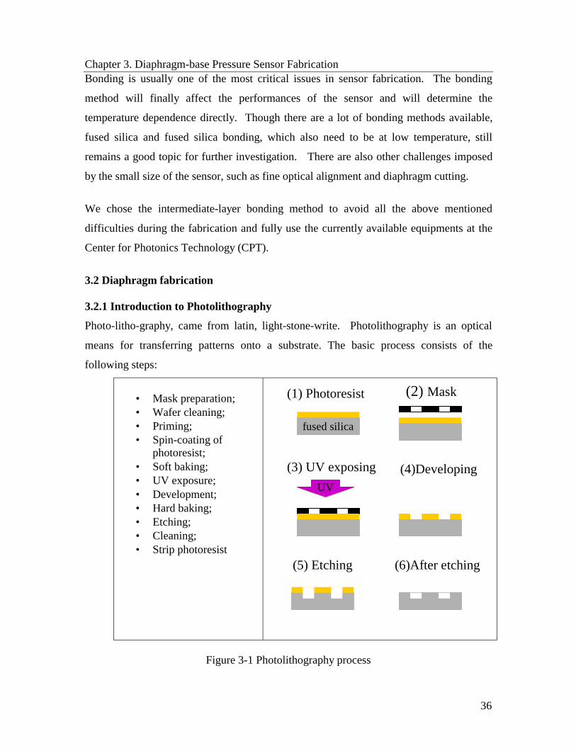
3.2 Diaphragm fabrication 3.2.1 Introduction to Photolithography
Photo-litho-graphy, came from latin, light-stone-write. Photolithography is an optical
means for transferring patterns onto a substrate. The basic process consists of the
following steps:
• Mask preparation; • Wafer cleaning; • Priming; • Spin-coating of
photoresist; • Soft baking; • UV exposure; • Development; • Hard baking; • Etching; • Cleaning; • Strip photoresist
Figure 3-1 Photolithography process
fused silica
UV
(1) Photoresist (2) Mask
(3) UV exposing (4)Developing
(5) Etching (6)After etching

Chapter 3. Diaphragm-base Pressure Sensor Fabrication
37
Step 1. Mask preparation
A piece of copper plate or other materials that can block the UV light can be used as a
mask. In this experiment, the transparency printed out with patterns is used as a mask.
This is an economical mask-making method.
Step 2. Wafer Cleaning
Typical contaminants that must be removed prior to photoresist coating is:
• dust from scribing or cleaving(minimized by laser scribing);
• atmospheric dust (minimized by good clean room practice);
• abrasive particales (from lapping);
• lint from wipers (minimized by using lint-free wipers);
• photoresist residue from previous photolithography (minimized by performing
oxygen plasma ashing);
• bacteria (minimized by good DI water system);
• films from other sources: solvent residue, H2O residue, photoresist or developer
residue, oil, silicon.
The standard degrease procedure is:
- 2-5 min. soak in diluted H2SO4 (<5%) with ultrasonic agitation
- 2-5 min. soak in DI H2O with ultrasonic agitation
- 2-5 min. soak in acetone with ultrasonic agitation
- 30 sec. Rinse under free flowing DI H2O
- dry with a heat gun or hotplate(~100°C)
Step 3. Priming
Primer is an adhesion promoter, used to assist photoresist coating. Hexamethyldisilazane
(HDMS) is the industry’s most widely used and accepted adhesion promoter. It may be
applied in vapor, liquid or solution form to reduce surface energy, provide excellent
surface coverage, and reduce underetch and lifting of photoresist.
HMDS (AP010 from Silicon Resources, Inc.) can be applied to substrate, spraying or
dipping. Wet application is accomplished by applying HMDS directly to a wafer and
Chapter 3. Diaphragm-base Pressure Sensor Fabrication
38
spinning at 3000-5000rpm. Excess material is spun off and a subsequent hot plate bake
(100~150°C) will complete the priming sequence. The bake temperature chosen depends
on the photoresist we use. For AZ TFP 650, the priming bake temperature should be as
high as 150°C.
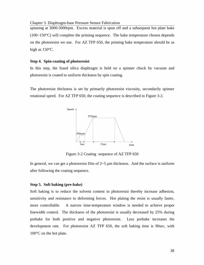
Step 4. Spin-coating of photoresist
In this step, the fused silica diaphragm is held on a spinner chuck by vacuum and
photoresist is coated to uniform thickness by spin coating.
The photoresist thickness is set by primarily photoresist viscosity, secondarily spinner
rotational speed. For AZ TFP 650, the coating sequence is described in Figure 3-2.
Figure 3-2 Coating sequence of AZ TFP 650
In general, we can get a photoresist film of 2~5 µm thickness. And the surface is uniform
after following the coating sequence.
Step 5. Soft baking (pre-bake)
Soft baking is to reduce the solvent content in photoresist thereby increase adhesion,
sensitivity and resistance to deforming forces. Hot plating the resist is usually faster,
more controllable. A narrow time-temperature window is needed to achieve proper
linewidth control. The thickness of the photoresist is usually decreased by 25% during
prebake for both positive and negative photoresist. Less prebake increases the
development rate. For photoresist AZ TFP 650, the soft baking time is 90sec, with
100°C on the hot plate.
Speed
time
200rpm
970rpm
3sec 15sec

Chapter 3. Diaphragm-base Pressure Sensor Fabrication
39
Step 6. UV exposure and development
Align the mask to the diaphragm. The exposure by applying UV radiation decomposes a
development inhibitor and developer solution only dissolves photoresist in the exposed
area. The exposure time depends on the thickness of the photoresist. In general, we
exposure the diaphragm for 60 seconds and immerse the diaphragm in the developer for
20 second for AZ TFP 650.
Step 7. Hard baking (post-bake)
Hard baking is to remove the solvent content in photoresist thereby increasing adhesion,
hardening the photoresist and making it etch resistant. The hard baking time for
photoresist AZ TFP 650 is 120 seconds with 120°C on the hot plate.
Step 8. Etching
Etching can be described as pattern transfer by chemical/physical removal of a material
from a substrate, often in a pattern defined by a protective mask layer (e.g., a resist or an
oxide). Mask-based etching is divided into dry etching and wet etching. Wet etching is a
technique that etching is in the liquid phase. Compared to the dry etching, wet chemical
etching provides a higher degree of selectivity. Wet etching often is faster and cheaper.
In our experiments, we use buffered hydrogen fluoride (BHF) as etchant. HF-based
etchants are used mainly for silicon dioxide, because they were observed to etch
polysilicon very slowly, but other researchers have noticed that various solutions attach
polysilicon at the grain boundaries, resulting in noticeable surface roughness. Research
indicates that HF can diffuse through thin polysilicon to etch underlying low-temperature
oxide. For pure HF etching, the overall reaction is
SiO2 + 6HF → H2SiF6 +2H2O
HF is a weak acid, except when present in very small concentrations, it does not
completely dissociate into H+ and F- ions in water. The etch rate of both silicon dioxide
and silicon nitride increase linearly with the concentrations of both HF and HF2-, while
being independent of the concentration of F- ions alone. The HF2- complex attacks oxide

Chapter 3. Diaphragm-base Pressure Sensor Fabrication
40
about 4.5 times faster than HF. Higher-order complexes, such as H2F3-, appear to occur
at higher HF concentrations (e.g. 49%HF) and attack oxide even faster than HF2-. Thus,
the etch rate increase faster than linearly with HF concentration. [19]
Acidic ammonium fluoride solution is called buffered hydrogen fluoride (BHF). The
chemical composition of BHF is usually a mixture of 40% NH4F and 49% or 50% HF,
ranging in weight ratios of NH4F: HF from 5:1 to 30:1. In buffered HF solutions, for pH
values above about 1, the concentration of HF2- is greater than that of HF. For more
acidic solutions, there is sufficient hydrogen to combine with the fluoride to make HF the
dominant species. As HF and HF2- are consumed, the etch rate decreases. Buffering with
NH4F helps keep the pH and thus the concentrations of HF and HF2- constant, stabilizing
the etch rate. BHF is widely used as a surface treatment agent for the process of
etching. [18]
Step 9. Cleaning and Strip photoresist
DI H2O is used to clean the diaphragm. Rinse the diaphragm in for 2 minutes. Acetone
is used to strip photoresist (PR) and for lift-off patterning of films. Lift-off processes can
be sped up by heating the acetone or by placing it in an ultrasonic bath.
3.2.2 Deep wet etching on fused silica diaphragm Following the above photolithography process, we can get a very good etched pit on the
fused silica, as we can see from Figure 3-3. But the etch depth can be only up to 5
micron. Currently no photoresist can withstand BHF for long time (more than 1 hour).
In our experiment, we need to etch deeper pits to increase the dynamic range for pressure
testing. The etch depth of at least 15 µm is required.

Chapter 3. Diaphragm-base Pressure Sensor Fabrication
41
Figure 3-3 Wet etched pit on the fused silica diaphragm 3.2.2.1 Chromium layer for deep wet etching For deeper structures, the photoresist does not withstand HF solution long enough. Thus
additional masking layers that can be deposited onto glass have to be used. This mask
layer should be deposited between the photoresist layer and the wafer in order to further
protect the wafer surface from HF attack. We choose to use Chromium as the metal
mask for several reasons:
• We have a sputtering system available for Chromium coatings;
• Chromium targets for the sputtering system are relatively cheap;
• Chromium layers can improve the adhesion of the photoresist to the diaphragm
and prevent HF acid attack the diaphragm;
• Chromium layers can be easily removed by a commercial chromium mask etchant
3.2.2.2 Deep wet etch process
In order to deep etch on a fused silica diaphragm, several additional steps related with
Chromium coating and Chromium layer removal are used. The whole process is shown
in Figure 3-4.

Chapter 3. Diaphragm-base Pressure Sensor Fabrication
42
(a) (b) (c) (d) (e) (f) (g) Photoresist Chromium
Figure 3-4 Deep wet etch process
a) Deposit Chromium onto the diaphragm;
b) Spin coating photoresist;
c) UV expose and develop;
d) Remove partial Chromium layer without photoresist protection
e) Wet etch by BHF;
f) Remove photoresist;
g) Remove Chromium layer
3.2.2.3 Deposit Chromium layer by sputtering
Sputtering is a technology in which the material is released from the source at much
lower temperature than thermal evaporation. The substrate is placed in a vacuum
chamber with the source material, named a target, and an inert gas (such as argon) is
introduced at low pressure. A gas plasma is struck using an RF power source, causing the
gas to become ionized. The ions are accelerated toward the surface of the target, causing
atoms of the source material to break off from the target in vapor form and condense on
all surfaces including the substrate. As for evaporation, the basic principle of sputtering is
the same for all sputtering technologies. The differences typically relate to the manor in
which the ion bombardment of the target is realized. A schematic diagram of a typical RF
sputtering system is shown in Figure 3-5. [4]

Chapter 3. Diaphragm-base Pressure Sensor Fabrication
43
Figure 3-5 Typical RF sputtering system [4]
The coating thickness of a chromium layer depends on the RF power, the process
pressure and the deposit time. The following is the results of chromium coatings at
different conditions:
Power (W) Time (Second)
Pressure (Torr) Thickness (nm)
100 15 3.5e-3 10 100 30 3.6e-3 55 100 60 3.6e-3 70 300 60 3.4e-3 180 Table 3-1 Chromium Coating Thickness vs. Coating Conditions
3.2.2.4 Deep wet etch results
The following plot presents a diaphragm etched in BHF for 5 hours. The etched depth is
about 25 micron. We can see from figure 3-6, the sidewall of the pit is still steep and the
surface inside the pit is flat. Sensors made by these pits can have an interference fringe
visibility as high as 98%. Even deeper pits can be etched using this method.
Figure 3-6 Etch result of deep wet etching
RF signalWater CooledSputter Target
Wafer
Gas Inlet Vacuum pump
Counter electrodePLASMA

Chapter 3. Diaphragm-base Pressure Sensor Fabrication
44
3.2.3 Two-step chemical etching on fused silica diaphragm
The center of the pit on the diaphragm is the most sensitive part. The central axis of the
ferrule and the center of the pit should be aligned in order to reach the maximum
sensitivity of the pressure. In Figure 3-7, a 3-D computer simulation of diaphragm
deflection is presented by using Equation (2.39). In this simulation, the diameter of
etched pit is 1mm, and the pressure is 800 psi, and the thickness of the diaphragm is 95
µm.
Figure 3-7 Computer simulation of fused silica diaphragm deflection
A two-step etching structure is used to make the alignment of the tube with the pit on the
diaphragm easy to operate. The larger diameter is the same size of the OD of the ferrule
(Figure 3-8). The ferrule can be put into the larger pit and the center of the ferrule will be
automatically align with the center of the smaller etched pit which forms the interference
cavity with the fiber end inserted into the ferrule.
Figure 3-8 Two step etch to solve alignment problem
Chapter 3. Diaphragm-base Pressure Sensor Fabrication
45
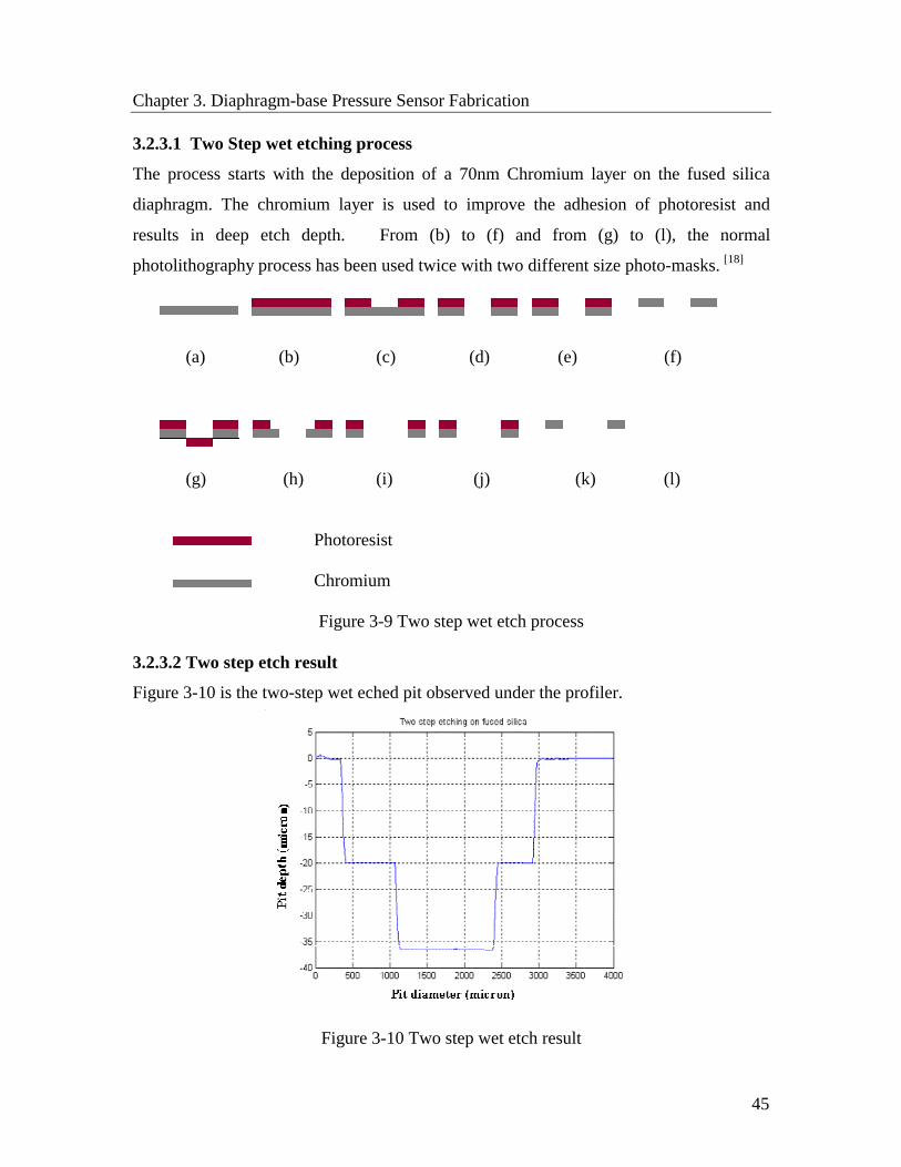
3.2.3.1 Two Step wet etching process
The process starts with the deposition of a 70nm Chromium layer on the fused silica
diaphragm. The chromium layer is used to improve the adhesion of photoresist and
results in deep etch depth. From (b) to (f) and from (g) to (l), the normal
photolithography process has been used twice with two different size photo-masks. [18]
(a) (b) (c) (d) (e) (f) (g) (h) (i) (j) (k) (l)
Photoresist
Chromium
Figure 3-9 Two step wet etch process 3.2.3.2 Two step etch result
Figure 3-10 is the two-step wet eched pit observed under the profiler.
Figure 3-10 Two step wet etch result

Chapter 3. Diaphragm-base Pressure Sensor Fabrication
46
3.2.4 Wet chemical etch results analysis 3.2.4.1 Etch rate The wet etch rates can vary for reasons that are usefully divided into three groups: the
etch setup, the material being etched, and the layout and structure on the substrate. The
most significant effects on wet-etch rates are as follows:
• Temperature;
• Impurities in or on the material being etched;
• Contamination
For fused silica, the etch rate in 5:1 BHF at the room temperature is about 46.42nm per
minute.
0 200 400 600 800 1000-5
0
5
10
15
20
25
30
35
40
Etch
Dep
th (
mic
ron)
Time (minute)
Rm Temp Linear Fit
Figure 3-11 Etch rate of 5:1 BHF
If we choose to use the commercially available BHF etchant (Sigma Aldrick, Ammonium
fluoride-hydrofluoric acid mixture, 35.1% NH4F, 6.3% HF), the etch rate on fused silica
at room temperature is 83.3nm per minute.
We can also notice that the total etch rate curves are not linear. After certain amount of
time, the etch rate decreased a little. As we mentioned in previous sections, HF
molecules and HF2- ions are consumed with time and make the HF concentration smaller
than it was at the very beginning. If we do want to etch a sample in BHF solution for long
time, bigger container with more BHF solution is suggested.

Chapter 3. Diaphragm-base Pressure Sensor Fabrication
47
180 200 220 240 260 280 300
14000
16000
18000
20000
22000
24000
26000
Etch
Dep
th (n
m)
Etch Time (Minute)
Figure 3-12 Etch rate of commercial BHF
3.2.4.2 Surface roughness The amount of ammonium fluoride (NH4F) in BHF solution is the most important factor that affected the surface cleanness. Some pin holes appeared on the etched diaphragm if we didn’t mix enough with NH4F. The smoothness of the surface can be ensured through wet etching by the improvement of the compositions of the BHF solution. For the left plot in Figure 3-13, we mix H2O, HF4F and HF with the percentage of 58%: 20%:22% and for the right plot in Figure 3-13, the concentration ratio changed to be:H2O: NH4F: HF = 58%:36%:6%. We can see from the two plots in Figure 3-13 that the surface quality in the second plot is significantly improved by changing BHF composition.
Figure 3-13 Surface quality improvement

Chapter 3. Diaphragm-base Pressure Sensor Fabrication
48
Also, the lower concentration of the HF, the better surface quality we can get. So
chemical etching is a possible means to mitigate the growth of surface damage on fused
silica.
There is a trade-off between surface quality and etch rate. For our sensor fabrication, we
finally choose commercially available BHF with higher concentration to etch the small
size pit. The etch rate is high and we can get as deep as 20 µm pits in 4 hours. But the
etched surface became a little bit rough after so long time etching as shown in Figure 3-
13 (2nd plot). Then we used 10:1 BHF to etch the larger size pits. Since we don’t care
much about the depth of the larger pits and lower concentrate of HF can mitigate the
surface roughness of the small pits caused by the first etch process.
The reflectance of the etched pit on the fused silica diaphragm can be as high as 4% with normal light incidence.
Picture from Surface Profiler Picture from Microscope
Table 3-2 Pictures of Etched Pit 3.2.4.3 Diameter Deviation
The main factor that affects the diameter of the etched pit is the UV exposure process
including the distance between the UV light source and the substrate and the exposure
time. Ideally, different areas of the substrate should be exposed by the same energy and
Black area is Chromium coating
White curve is the scan result of the etched pit

Chapter 3. Diaphragm-base Pressure Sensor Fabrication
49
the same period. If we put the UV light too close to the substrate (Figure 3-14, left),
some areas were over-exposed and some other areas were under-exposed because of the
limited size of the UV light. This caused the diameter of the size to vary a lot.
Figure 3-14 UV light exposure If we place the UV light source far away from the substrate, the exposure would be more
uniform as illustrated in Figure 3-14 (right plot). But longer exposure time is needed. In
this experiment, the distance between the UV light and the substrate is 8 cm and the
exposure time is 4 minutes.
The other factor that has some effects on the diameter size is the etching process. We can
see from the plot in Figure 3-15 that the sidewalls of the 2nd pit are very straight and
smooth. Therefore, the deviations of the etched pit diameter are reduced. We can see that
in the second plot the diameter deviation is: (1.14-1.04)/1.04*100%= 9.6%, but in the
first plot, the diameter deviation is: (1.8-1.04)/1.04*100%=73%. The sensitivity of the
sensor can be better controlled with the reduced deviation of the pit diameter per our
calculation in the diaphragm design section.
UV light
Beams
Substrate
UV light
Beams
Substrate

Chapter 3. Diaphragm-base Pressure Sensor Fabrication
50
Figure 3-15 Diameter Deviation
3.2.4.4 Etch depth uniformity
Figure 3-16 shows two etched pits on two different diaphragms measured by a surface
profiler. These two diaphragms were both etched in the commercial BHF for 5 hours
respectively. The etch depth was controlled by BHF concentration, the temperature and
the time. Since HF is extremely dangerous, we normally only use it under the room
temperature. And commercial BHF is used in order to keep the BHF concentration
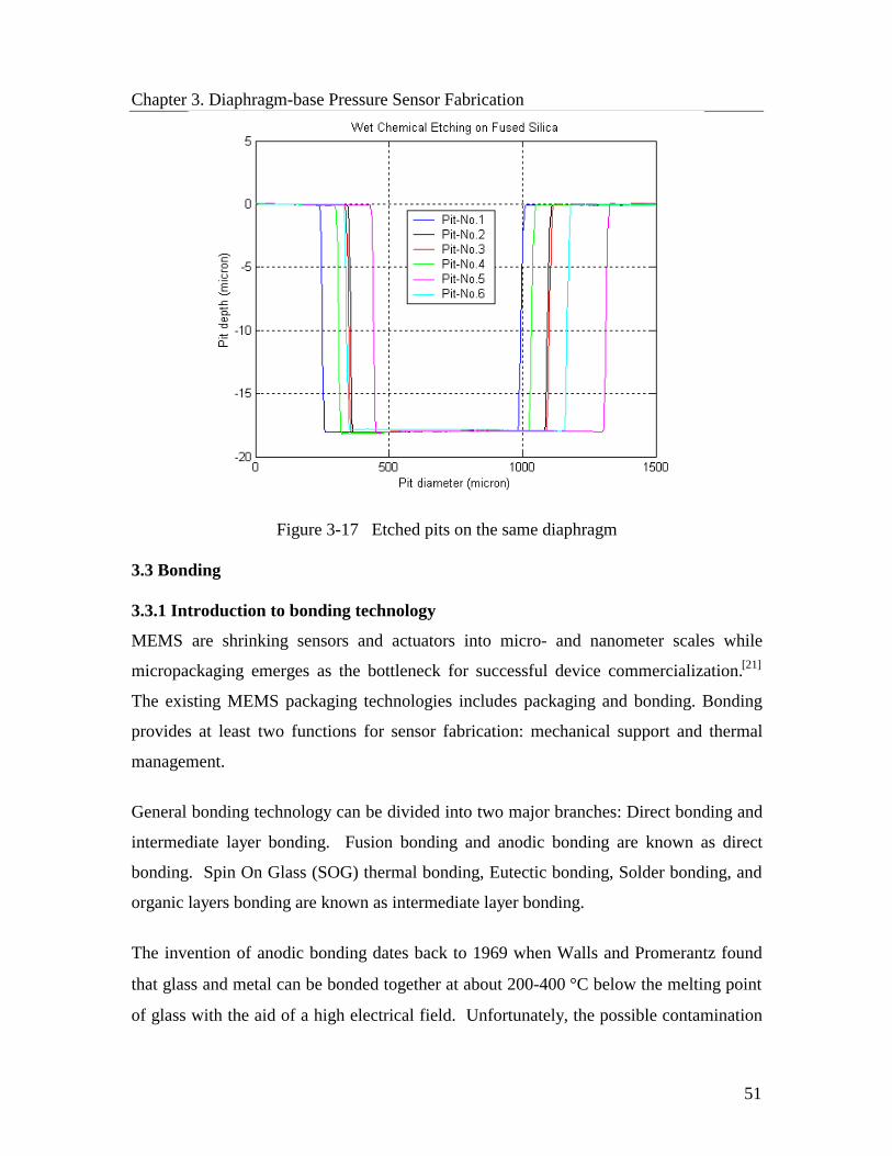
unchanged. Figure 3-17 shows six etched pits on the same diaphragm measured by a
surface profiler.
Figure 3-16. Etched pits on two different diaphragms
Chapter 3. Diaphragm-base Pressure Sensor Fabrication
51
Figure 3-17 Etched pits on the same diaphragm 3.3 Bonding 3.3.1 Introduction to bonding technology
MEMS are shrinking sensors and actuators into micro- and nanometer scales while
micropackaging emerges as the bottleneck for successful device commercialization.[21]
The existing MEMS packaging technologies includes packaging and bonding. Bonding
provides at least two functions for sensor fabrication: mechanical support and thermal
management.
General bonding technology can be divided into two major branches: Direct bonding and
intermediate layer bonding. Fusion bonding and anodic bonding are known as direct
bonding. Spin On Glass (SOG) thermal bonding, Eutectic bonding, Solder bonding, and
organic layers bonding are known as intermediate layer bonding.
The invention of anodic bonding dates back to 1969 when Walls and Promerantz found
that glass and metal can be bonded together at about 200-400 °C below the melting point
of glass with the aid of a high electrical field. Unfortunately, the possible contamination

Chapter 3. Diaphragm-base Pressure Sensor Fabrication
52
due to excessive alkali metal in the glass; possible damage to microelectronics due to the
high electrical field; and the requirement of flat surface for bonding limit the application
of anodic bonding to MEMS. Furthermore, for our sensor fabrication, anodic bonding
cannot be applied because this method cannot work between fused silica and fused silica.
Fusion bonding is mostly used in silicon-on-insulator (SOI) technology such as Si-SiO2
bonding and silicon-silicon bonding. It is a proven method and the bonding strength is
enormously strong. Unfortunately, since the temperature requirement is generally higher
than 1000°C, it may not suitable for our sensor fabrication because the gold coating on
both interference cavity surfaces may have to be used to improve the reflectance. Such a
high temperature can severely damage the gold coating films.
Eutectic bonding, which is based on the use of bonding materials that form a eutectic
alloy in specific temperature conditions, has been used widely in microfabrication. It
provides high bonding strength and good stability at a relatively low bonding temperature
at 363°C. But this method is difficult to obtain complete bonding over large surface
areas, and even native oxides prevent bonding from taking place and eutectic bonding is
reported to introduce substantial mounting stress in piezoresistive sensors, causing long-
term drift due to relaxation of the built-in stress.
Solder bond technology is widely used in the connection to chip process in IC packaging.
Solders are often used to bond two metals together in electrical engineering. Because
solders have reasonably good mechanical strength, the bonding is usually solid and
stable. The disadvantage of solder bonding is that most of the solder cannot withstand
high temperature.
There are also some other intermediate layer bonding technologies, such as: SOG thermal
bonding, Epoxy bonding and Intermediate layer borosilica glass bonding. All the
intermediate layer bonding methods have the same disadvantage that the coefficients of
thermal expansion and Young’s modulus of the intermediate layer material are different
from that of the fused silica components in the sensor. This difference causes very poor
temperature stability of the sensor and bonding is not real physically ‘solid’.
Chapter 3. Diaphragm-base Pressure Sensor Fabrication
53
3.3.2 SOL-GEL intermediate layer bonding
It seems that, the direct bonding of a fused silica ferrule and a fused silica diaphragm is
the most promising way to reduce the temperature dependence. However, there are two
reasons not to choose the direct bonding.
It is well known that “intimate contact” and “temperature” are two major factors for
direct bonding “Intimate contact ” puts two separated surfaces together and
“temperature” provides the bonding energy.
On intimate contact, though we can successfully bond two fused silica wafers together,
directly bonding a patterned diaphragm to a flat substrate, directly bonding a patterned
diaphragm and a ferrule still faces a number of challenges and is currently under
investigation at the Center for Photonics Technology.
On temperature side, fusion bonding and anodic bonding require high temperatures that
may damage the gold coatings we may have to use to increase the reflectance.
Using the intermediate layer bonding seems a natural choice in our research. Sol-gel is
chosen to be as the intermediate layer for several reasons:
• Sol-gel is a low temperature process;
• Thin films can be formed by sol-gel process;
• The final form of sol-gel process “gel” can be high purity silica, which will
reduce the thermal expansion of the intermediate layer;
• Sol-gel can be made in our lab and it is a cheap process
In our reseach, sol-gel is used for both the diaphragm-to-ferrule bonding and the ferrule-
to-fiber bonding.
3.3.2.1 SOL-GEL process
The term sol-gel was first coined in the late 1800s. It generally refers to a low-
temperature method using chemical precursors that can produce ceramics and glasses

Chapter 3. Diaphragm-base Pressure Sensor Fabrication
54
with better purity and homogeneity than high temperature conventional processes. In
general, the sol-gel process involves the transition of a system from a liquid “sol” (mostly
colloidal) into a solid ”gel” phase (usually silica). Applying the sol-gel process, it is
possible to fabricate ceramic or glass materials in a wide variety of forms: ultra-fine or
spherical shaped powders, thin film coatings, ceramic fibers, microporous inorganic
membranes, monolithic ceramics and glasses, or extremely porous aerogel materials.
Thin films can be produced on a piece of substrate by spin-coating or dip-coating. When
the “sol” is cast into a mold, a wet “gel” will form. With further drying and heat-
treatment, the “gel” is converted into dense ceramic or glass articles. The basic sol-gel
reaction, shown in Figure 3-18, consists of two chemical reactions that produce a thin
film when the sol is applied to a substrate. The first is a hydrolysis reaction and the
second is a condensation reaction. The hydrolysis reaction produces the sol, and then, in
the condensation reaction, a macroscopic gel is formed on the substrate producing a thin
film.
Figure 3-18 Basic sol-gel reaction
This basic sol-gel reaction starts when the metal alkoxide Si(OCH2CH3)4
(tetraethoxysilane, or TEOS) is mixed with H2O and a hydrolysis reaction occurs. TEOS
is used because it, along with other metal alkoxides, reacts readily with water. Ethanol is
used as a solvent because water and alkoxides are immiscible. Providing there is
sufficient water and a catalyst present, the hydrolysis reaction will be completed when all
of the (OCH2CH3) groups are replaced by (OH):
Si(OCH2CH3)4 + 4H2O à Si(OH)4 + 4CH3CH2OH
producing a sol consisting of Si(OH)4 (silicic acid) and CH3CH2OH (ethanol). Next, two partially hydrolyzed molecules can link together in a condensation reaction
that liberates water:
Precursors SOL GELHydrolysis Condensation

Chapter 3. Diaphragm-base Pressure Sensor Fabrication
55
2Si(OH)4 à (OH)3Si—O—Si(OH)3 + H2O
As the reaction proceeds, the number of Si—O—Si bonds increases in a process called
polymerization, which produces a macroscopic gel. When producing thin films this gel is
formed by rapid evaporation of the solvent.
3.3.2.2 Diaphragm-ferrule bonding Sol-gel is liquid. It expands, flows and cannot be controlled easily. There are two
possible ways to apply sol-gel between the diaphragm and the ferrule. One is spin
coating the sol-gel onto the diaphragm. The other way is apply sol-gel onto the ferrule
end and keep the diaphragm clean. We finally choose the second way because the spin
coated sol-gel layer will also cover the etched pits and contaminate the bottom surface of
etched pits.
The whole process of bonding diaphragm and the ferrule is shown as Figure 3-19.
Figure 3-19 Sol-gel bonding process
As we can see from Figure 3-20, the bonding area is the area with sol-gel. The sol-gel
area can even be a little bit larger than the etched pit as long as the inside hole of the
ferrule is not blocked. A micro-motion three dimentional positioning stage with a
monitor system is used to do the alignment. The bonding result is observed under the
microscope and is shown as Figure 3-21.
Apply sol-gel onferrule end
AlignmentFerrule inside hole –
Pit center on the diaphragmHeat
(Hot plate: 250 degree C)

Chapter 3. Diaphragm-base Pressure Sensor Fabrication
56
Figure 3-20 Apply sol-gel on the ferrule end
Figure 3-21 Sol-gel bonded diaphragm and ferrule
3.3.2.3 Ferrule-fiber bonding
The last step of the sensor fabrication is to insert the fiber into the ferrule, adjust the air-
gap and bond them together. In this step, sol-gel is dip-coated around the surface of the
fiber, and heated by using CO2 laser with very low power for about several seconds.
Any heat method, such as the use of a heat gun, a hot plate, a furnace or a laser can work,
but after the air-gap adjustment, both the fiber and the ferrule should be kept relatively
unmoved on the positioning system during the heating. Because of this requirement, the
CO2 laser based heating method is adopted.
OD=1.8mm
Pit diameter1.0mm
Ferrule ID:127um+/- 1um
Sol-gel
Chapter 3. Diaphragm-base Pressure Sensor Fabrication
57
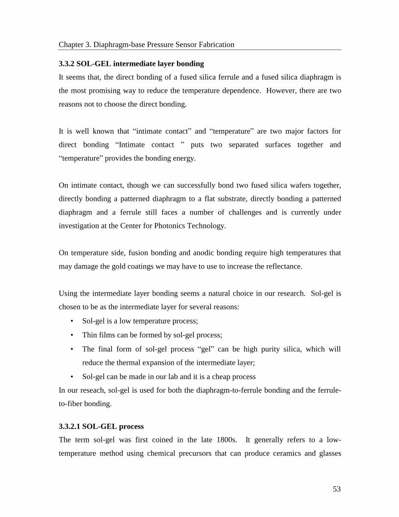
3.4 Sensor fabrication 3.4.1 Principle of White light interferometric Sensor Cavity length Monitoring
System
In the process of the sensor fabrication, we use the white light fiber interferometric
system, which was developed by the Center of Photonics Technology (CPT), to monitor
the length of the interference cavity. The measurement of the sensor cavity length is
achieved by demodulating the interference spectrum of the SCIIB sensor.
The basic principle of the white light interferometric sensor cavity length monitoring can
be illustrated using Figure 3-22. When the sensor is fabricated, the fiber end and the
diaphragm surface will generate an interference signal which is transmitted back to the
spectrometer through a 2x2 fiber coupler.
Figure 3-22 Basic principle of the white light interferometric sensor cavity length monitoring
If we assume that the broadband light source (LED or SLED) has a Gaussian spectral
power distribution given by
( )20
0 2( ) exp( )sI Iλ λ
λλ
− −=
∆ (3-1)
where 0λ is the central wavelength, 0I is the peak value, and λ∆ is the source spectral
width. The output interference signal is then given by:
042 1 ( ) cos( )s
LI I L πγ ϕ
λ = + +
(3-2)
PCSpectrometer Index
matching gel
3 dB Fibercoupler
Broadbandsource
Fiber sensorprobe
Chapter 3. Diaphragm-base Pressure Sensor Fabrication
58
where the factor γ takes into account the decreased visibility due to the numerical
aperture of the fiber as well as other attenuating effects, and 0ϕ is the initial phase
difference between the two interference signals.
If we normalized the interference spectrum given by Equation (3-2) with respect to the
source spectrum, we have the normalized interference output expressed as
042 1 ( ) cos( )LI L π
γ ϕλ
= + + (3-3)
It is shown in Equation (3-3) that the output spectrum of the sensor is modulated by a
sinusoidal function due to the interference. Because the interference spectrum is a
function of the sensor cavity length L, the successful demodulation of this spectral signal
can render an accurate and absolute measurement of the sensor cavity length.
A simple case can be considered in which two different spectral components of the
source (λ1 and λ2) are utilized. These two wavelength components arrive at the
spectrometer with different phases, which can be expressed as
1 01
4 Lπϕ ϕ
λ= +
2 02
4 Lπϕ ϕ
λ= + (3-4)
Thus the phase difference between these two spectral components is given by
1 21 2
1 2
4 ( )Lπ λ λϕ ϕ ϕ
λ λ−
∆ = − =×
1 21 2
1 2
4 ( )Lπ λ λϕ ϕ ϕ
λ λ−
∆ = − =×
(3-5)
Rewriting Equation (3-5), we have
1 2
1 24 ( )L ϕ λ λ
π λ λ∆ × ×
=−
1 2
1 24 ( )L ϕ λ λ
π λ λ∆ × ×
=−
(3-6)
Although it is not easy to measure the phase difference of two arbitrary spectral
components, there exist a few special points with fixed phase relation. For example, the
phase difference between two adjacent peaks (or valleys) is 2π. Therefore, by detecting
the spectral locations of the peaks or valleys in the interference spectrum, we can obtain
the cavity length L by applying Equation (3-6).
Chapter 3. Diaphragm-base Pressure Sensor Fabrication
59
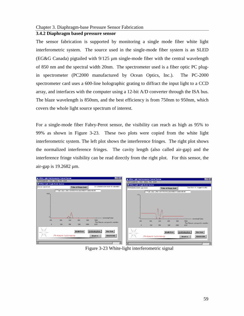
3.4.2 Diaphragm based pressure sensor
The sensor fabrication is supported by monitoring a single mode fiber white light
interferometric system. The source used in the single-mode fiber system is an SLED
(EG&G Canada) pigtailed with 9/125 µm single-mode fiber with the central wavelength
of 850 nm and the spectral width 20nm. The spectrometer used is a fiber optic PC plug-
in spectrometer (PC2000 manufactured by Ocean Optics, Inc.). The PC-2000
spectrometer card uses a 600-line holographic grating to diffract the input light to a CCD
array, and interfaces with the computer using a 12-bit A/D converter through the ISA bus.
The blaze wavelength is 850nm, and the best efficiency is from 750nm to 950nm, which
covers the whole light source spectrum of interest.
For a single-mode fiber Fabry-Perot sensor, the visibility can reach as high as 95% to
99% as shown in Figure 3-23. These two plots were copied from the white light
interferometric system. The left plot shows the interference fringes. The right plot shows
the normalized interference fringes. The cavity length (also called air-gap) and the
interference fringe visibility can be read directly from the right plot. For this sensor, the
air-gap is 19.2682 µm.
Figure 3-23 White-light interferometric signal