design, simulation, and fabrication of a flow sensor for
TRANSCRIPT

Rochester Institute of TechnologyRIT Scholar Works
Theses Thesis/Dissertation Collections
12-1-2009
Design, simulation, and fabrication of a flow sensorfor an implantable micropumpMatthew J. Waldron
Follow this and additional works at: http://scholarworks.rit.edu/theses
This Thesis is brought to you for free and open access by the Thesis/Dissertation Collections at RIT Scholar Works. It has been accepted for inclusionin Theses by an authorized administrator of RIT Scholar Works. For more information, please contact [email protected].
Recommended CitationWaldron, Matthew J., "Design, simulation, and fabrication of a flow sensor for an implantable micropump" (2009). Thesis. RochesterInstitute of Technology. Accessed from

Design, Simulation, and Fabrication of a Flow Sensor
for an Implantable Micropump
by
Matthew J. Waldron
A Graduate Thesis Submitted in Partial Fulfillment
of the Requirements for the Degree of
MASTER OF SCIENCE
in
Electrical Engineering
Approved by:
Dr. David Borkholder, Thesis Advisor
Dr. James Moon, Committee Member
Dr. Lynn Fuller, Committee Member
Dr. Sohail Dianat, Department Head
DEPARTMENT OF ELECTRICAL AND MICROELECTRONIC ENGINEERING
KATE GLEASON COLLEGE OF ENGINEERING
ROCHESTER INSTITUTE OF TECHNOLOGY
ROCHESTER, NEW YORK
December 2009

ABSTRACT
The design, simulation, and fabrication of a flow sensor to be integrated into an implantable micropump is presented. The flow sensor operates by the method of thermal anemometry, in which heat is dissipated from a resistive element held in the flow of the fluid. The rate at which heat is carried away is dependent on the flow rate and is directly related to the thermal conductance. A control circuit utilizing the constant-temperature anemometry mode of operation is used to generate a change in voltage in response to change in thermal conductance, and subsequently, flow rate. A mathematical expression describing the sensor sensitivity based on thermal effects is proposed, based on the thermal spreading resistance and basic heat transfer laws. The mathematical model is refined using finite-element analysis, and a complete formulation for the effect of sensor area, length-to-width ratio, and fluid velocity on thermal spreading resistance is determined. The refined thermal spreading conductance equation can be used to replace assumptions made in initial mathematical analysis. An original fabrication process is presented and investigated, in which a p-doped polysilicon bridge is encapsulated in silicon oxide and silicon nitride using surface micromachining techniques. A sacrificial polysilicon layer and KOH etching are used to form half of the complete fluid channel in the bulk of the silicon wafer. When the fluid channel is sealed with a complementarily etched wafer, the sensor bridge is situated in the middle of the fluid channel, optimally placed for maximum sensitivity. The fabrication process yields functional sensor bridges, with even the most fragile sensor shape withstanding the process. An analog constant-temperature control circuit is developed, based upon a Wheatstone bridge with a feedback op-amp. The circuit produces an output voltage dependent on thermal resistance, and will reduce the effect of fluid temperature fluctuations on circuit output. This relies on introducing a second sensor bridge into the fluid channel, and limiting its self-heating. A design based on replacing one element in the Wheatstone bridge with a “transimpedance virtual resistor”, and another design based on reducing the power to one leg of the bridge are simulated, and their performance compared. PSPICE simulations are used to optimize the circuits in order to maximize the ratio of sensitivity to fluid velocity to sensitivity to ambient temperature.

i
TABLE OF CONTENTS
List of Tables .................................................................................................................................. ii List of Figures ................................................................................................................................ iii Chapter 1: Background ....................................................................................................................1 Chapter 2: Thermal Flow Measurement ..........................................................................................9 I. Modes of Operation ...........................................................................................................10 II. Sensor Design ....................................................................................................................13 Chapter 3: Physics of Operation ....................................................................................................19 I. Electrical Domain ..............................................................................................................21 II. Thermal Domain ................................................................................................................23 III. MATLAB Analysis............................................................................................................32 Chapter 4: Finite-Element Analysis...............................................................................................43 I. Simulation Setup................................................................................................................44 II. Thermal Spreading Conductance ......................................................................................47 III. Simulation of Entire System ..............................................................................................71 Chapter 5: Fabrication....................................................................................................................83 I. Fabrication Procedure and Process Details........................................................................84 II. Fabrication Yield .............................................................................................................109 Chapter 6: Signal-Conditioning Circuitry....................................................................................121 Chapter 7: Test Plan.....................................................................................................................145 I. Fluid Channel Formation .................................................................................................145 II. Thermal Characterization.................................................................................................148 Chapter 8: Coalescence of Results...............................................................................................152 I. Overall Sensitivity Prediction ..........................................................................................153 II. Future Work .....................................................................................................................156 Appendix A: MATLAB Scripts for Chapter 3 ............................................................................158 Appendix B: MATLAB Scripts for Chapter 4.............................................................................162 Appendix C: CGS Units...............................................................................................................174 Appendix D: 3D Fabrication Model ............................................................................................175
ii
LIST OF TABLES
Table 3.1: Sensor Geometry Parameters....................................................................................... 20
Table 3.2: Thermal Domain Parameters ....................................................................................... 25
Table 3.3: Fluid Property Variables.............................................................................................. 29
Table 3.4: Nominal Sensor Parameters in MATLAB Simulations............................................... 32
Table 4.1: Values of the Coefficients of the Quartic Function fitted to Simulation Data of Thermal Spreading Conductance........................................................................................... 58
Table 4.2: Values of the Coefficients of the Quartic Function with Additional Parameter for Area Dependence............................................................................................................................ 60
Table 4.3: Fitting Parameters for King’s Law Coefficient ........................................................... 65
Table 4.4: Results of Simulation with 32 µm Fluid Channel ....................................................... 77
Table 4.5: Results of Simulation with 60 µm Fluid Channel ....................................................... 79
Table 4.6: Results of Simulation with 100 µm Fluid Channel ..................................................... 80
Table 8.1 Sensitivities for Simulated Circuits in Chapter 6........................................................ 154
Table 8.2 Typical and Minimum Overall Sensitivities for Circuits in Chapter 6....................... 154
Table 8.3 Effect of Change in Ambient Temperature on Perceived Change in Flow Rate. ....... 155
iii
LIST OF FIGURES
Figure 1.1: Turbine flowmeter diagram........................................................................................... 2
Figure 1.2: Oval gear positive displacement flowmeter. ................................................................. 3
Figure 1.3: Orifice plate in a fluid channel with pressure taps. ....................................................... 4
Figure 1.4: Example of a microscale differential pressure sensor. .................................................. 4
Figure 1.5: Example of an electromagnetic flow sensor.................................................................. 5
Figure 2.1: Basic hot-wire anemometer diagram............................................................................. 9
Figure 2.2: Calorimeter type flow sensor. ..................................................................................... 10
Figure 2.3: Heat pulses observed from a thermal time-of-flight sensor. ....................................... 11
Figure 2.4: Example of a thermal anemometer in a fluid channel made from a silicon wafer and glass wafer. ............................................................................................................................. 16
Figure 3.1: Thermal anemometer diagram for electrical and thermal analysis. ............................ 19
Figure 3.2: Diagram of geometric variables. ................................................................................. 20
Figure 3.3: Electrical domain diagram. ......................................................................................... 21
Figure 3.4: Electrical characteristics vs. distance from channel wall for typical anemometer geometry. ................................................................................................................................ 22
Figure 3.5: Diagram of heat conduction. ....................................................................................... 23
Figure 3.6: Thermal equivalent circuit diagram. ........................................................................... 26
Figure 3.7: Thermal spreading resistance vs. length-to-width ratio with best-fit curves. ............. 27
Figure 3.8: Spreading resistance vs. logarithm of the length-to-width ratio. ................................ 28
Figure 3.9: Thermal conductance vs. flow rate.............................................................................. 33
Figure 3.10: Anemometer power dissipation vs. flow rate............................................................ 34
Figure 3.11: Anemometer voltage vs. flow rate. ........................................................................... 34
Figure 3.12: Thermal conductance vs. length-to-width ratio with constant area........................... 36
Figure 3.13: Thermal conductance vs. heater area with length-to-width ratio held constant........ 37
Figure 3.14: Thermal conductance vs. heater width. ..................................................................... 38
Figure 3.15: Thermal conductance vs. channel width. .................................................................. 39
Figure 3.16: Sensitivity vs. channel width..................................................................................... 40
Figure 4.1: ANSYS model of an anemometer in fluid channel..................................................... 44
Figure 4.2: Meshed ANSYS model. .............................................................................................. 45
Figure 4.3: ANSYS model with loads applied. ............................................................................. 46
Figure 4.4: Large and small rectangular prisms representing infinite half-space of fluid and heating element....................................................................................................................... 48
iv
Figure 4.5: Meshed rectangular prisms using finest smart sizing resolution................................. 49
Figure 4.6: Contour plot of temperature with fluid velocity fixed at zero..................................... 50
Figure 4.7: Vector plot of fluid velocity with maximum fluid velocity. ....................................... 51
Figure 4.8: Contour plot of temperature with maximum fluid velocity across the sensor. ........... 52
Figure 4.9: Contour plot of temperature along the direction of fluid flow. ................................... 52
Figure 4.10: Surface plot of thermal conductance versus length-to-width ratio and area at zero flow rate. ................................................................................................................................. 54
Figure 4.11: Surface plot of thermal conductance versus length-to-width ratio and area at 0.3 cm/sec. .............................................................................................................................. 55
Figure 4.12: Surface plot of the difference in thermal conductance at 0.3 cm/sec and zero flow versus length-to-width ratio and area. .................................................................................... 56
Figure 4.13: Surface plot of the ratio of thermal conductance at 0.3 cm/sec to zero flow versus length-to-width ratio and area................................................................................................. 57
Figure 4.14: Surface plot of the difference in thermal conductance at flow rate of 0.3 cm/sec and zero flow rate, calculated from fitted quartic function for thermal spreading conductance... 59
Figure 4.15: Surface plot of the difference in thermal conductance at flow rates of 0.3 cm/sec and 0, calculated from the fitted quartic function with area dependence for thermal spreading conductance. ........................................................................................................................... 61
Figure 4.16: Plot of curve fitting coefficients, C0, C1, C2, C4, and C5 versus flow velocity with linear trendlines. ..................................................................................................................... 62
Figure 4.17: Plot of curve fitting coefficients, C0, C1, C2, C4, and C5 versus flow velocity with second-order polynomial trendlines. ...................................................................................... 63
Figure 4.18: King’s Law coefficient, β, versus sensor area and length-to-width ratio fitted to the simulation data for thermal conductance................................................................................ 64
Figure 4.19: King’s Law exponent, χ, versus sensor area and length-to-width ratio fitted to the simulation data for thermal conductance................................................................................ 65
Figure 4.20: Relative sensitivity to fluid velocity at 0.15 cm/sec versus sensor area and thermal length to width ratio calculated using quartic fit of thermal conductance data. ..................... 68
Figure 4.21: Relative sensitivity to fluid velocity at 0.15 cm/sec versus sensor area and thermal length to width ratio calculated using the King’s Law fit of thermal conductance data. ....... 68
Figure 4.22: Sensor quality factor at 0.15 cm/sec versus sensor area and thermal length to width ratio calculated using the quartic fit of thermal conductance data. ........................................ 70
Figure 4.23: Sensor quality factor at 0.15 cm/sec versus sensor area and thermal length to width ratio calculated using the King’s Law fit of thermal conductance data. ................................ 70
Figure 4.24: Results of velocity magnitude component parallel to microchannel. ....................... 73
Figure 4.25: Results of temperature distribution in the fluid......................................................... 74
Figure 4.26: Temperature distribution on entire sensor and heating element. .............................. 74

v
Figure 4.27: Total thermal conductance vs. flow rate for ANSYS simulations. ........................... 75
Figure 4.28: Velocity dependent thermal conductance vs. flow rate............................................. 76
Figure 4.29: Velocity dependent thermal conductance for sensors in a 32 µm fluid channel....... 78
Figure 4.30: Velocity dependent thermal conductance for sensors in a 60 µm fluid channel....... 80
Figure 4.31: Velocity dependent thermal conductance for sensors in a 100 µm fluid channel..... 81
Figure 5.1: Color legend of materials in microfabrication. ........................................................... 84
Figure 5.2: Tensile and compressive wafer bending after deposition of silicon nitride. ............... 92
Figure 5.3: Fit of resistivity versus diffusion temperature for Emulsitone spin-on dopants. ........ 96
Figure 5.4: CDE ResMap analysis of N250 dopant diffused into polysilicon after second diffusion.................................................................................................................................. 96
Figure 5.5: CDE ResMap analysis of Borofilm 100 dopant diffused into polysilicon after second diffusion.................................................................................................................................. 97
Figure 5.6: Cross-sectional profile of KOH etch on (100) silicon............................................... 108
Figure 5.7: Cross-section of the complete anemometer fabrication process. .............................. 109
Figure 5.8: Microscope image of fabrication after step 34.......................................................... 110
Figure 5.9: Microscope image of fabrication after step 34 showing residue inhibiting the phosphoric acid etch. ............................................................................................................ 111
Figure 5.10: Microscope image of fabrication after completed fabrication showing residue remaining attached to bridges............................................................................................... 112
Figure 5.11: Microscope image showing typical sensor and fluid channel at difference focus depths.................................................................................................................................... 113
Figure 5.12: Microscope image of sensor after completed fabrication process. ......................... 114
Figure 5.13: SEM image of 60 µm fluid channel entrance......................................................... 115
Figure 5.14: SEM image of 32 µm fluid channel entrance......................................................... 115
Figure 5.15: SEM image of typical sensor in 100 µm fluid channel. .......................................... 116
Figure 5.16: SEM image of wide sensor in 60 µm fluid channel. .............................................. 116
Figure 5.17: SEM image of encapsulated serpentine polysilicon bridge. ................................... 117
Figure 5.18: SEM image of crease in layers at fluid channel edge. ............................................ 118
Figure 5.19: SEM image of sensor in 60 µm fluid channel to aluminum traces. ........................ 118
Figure 6.1: Basic Wheatstone bridge with constant bridge voltage............................................. 123
Figure 6.2: Wheatstone bridge with op-amp feedback. ............................................................... 124
Figure 6.3: Wheatstone bridge electrical circuit in PSPICE. The points RH+ and RH- represent connections to the thermal equivalent circuit. ...................................................................... 128
Figure 6.4: Anemometer thermal equivalent circuit in PSPICE.................................................. 128

vi
Figure 6.5: Heater circuit element coupling electrical circuit and thermal equivalent circuit..... 129
Figure 6.6: Wheatstone bridge with feedback op-amp with thermal properties of the heater resistor (right) and ambient temperature sensor (left) taken considered. ............................. 130
Figure 6.7: Transient simulation results of the circuit in Figure 6.6. .......................................... 131
Figure 6.8: DC Sweep simulation results of the circuit in Figure 6.6. ........................................ 131
Figure 6.9: Results of varying overheat temperature in Figure 6.6. ............................................ 132
Figure 6.10: Dependence of circuit sensitivity on overheat temperature. ................................... 133
Figure 6.11: Wheatstone bridge with feedback op-amp and thermal characteristics given to both the heating resistor and ambient temperature sensor............................................................ 134
Figure 6.12: Simulation results of circuit in Figure 6.11. The thermal resistance is swept on the x-axis. The upper plot shows the voltage of the op-amp output, and the lower plot shows the overheat temperature of the sensor. ...................................................................................... 134
Figure 6.13: Effect of changing the value of the ambient temperature sensor in Figure 6.11 on quality factor......................................................................................................................... 136
Figure 6.14: Wheatstone bridge with feedback amplifier circuit with ambient temperature sensor element replaced with transimpedance circuit...................................................................... 138
Figure 6.15: Output voltage of the circuit in Figure 6.14 versus thermal resistance................... 139
Figure 6.16: Effect of changing amplifier gain of diff amp 2 in the circuit in Figure 6.14 on quality factor......................................................................................................................... 140
Figure 6.17: Amplifier gain of diff amp 2 in the circuit in Figure 6.14 to produce maximum quality factor......................................................................................................................... 140
Figure 6.18: Wheatstone bridge with feedback amplifier and ambient side voltage reduction... 141
Figure 6.19: Output voltage of the circuit in Figure 6.18 versus thermal resistance with different ambient temperatures............................................................................................................ 142
Figure 6.20: Effect of changing amplifier gain in Figure 6.18 on quality factor......................... 143
Figure 7.1: Anisotropically etched silicon wafer bonded to isotropically etched glass wafer. ... 146
Figure 7.2: Schematic of complete constant-power characterization circuit............................... 149
Figure 7.3: Anemometer power from Figure 7.2......................................................................... 150
Figure 7.4: Determination of thermal resistance from electrical measurements. ........................ 151
1
BACKGROUND In microscale drug delivery systems, flow measurement performs a critical role in the pump feedback loop. In open-loop micropump systems, the pump behavior is initially characterized, and driven to deliver the amount of fluid desired. If the pump behavior degrades or changes over time, the pump’s ability to dispense a precise amount of fluid worsens. By adding a flow sensor to the pump control system, the system becomes closed-loop, and the pump can compensate for changes in behavior to dispense the desired amount of fluid. Micropumps, and microfluidics in general, have found a niche in biological and medical applications. Microfluidic assays can be used to assess the results of biological and chemical reactions using very small amounts of reactants. Implantable micropumps can be used to administer drugs over a long period of time, without the need for repeated injections, and breaching of the skin by needles ([6]). In drug-delivery systems, ensuring that the correct dose is administered is crucial, and in research applications when the dosage may need to be varied, the feedback provided by the flow sensor helps to ensure the accuracy of the experiment. A variety of methods exist to measure the fluid flow. At the macroscale and microscale, different design challenges are encountered, and flow measurement systems can have different advantages and disadvantages. The primary differences that arise are the ease of manufacturing, and the fluid flow regime. At a large size scale, more complex flow sensor designs can be manufactured, but turbulence in the flow is more common, causing unpredictable sensor response. At the microscale, the fluid flow is almost always laminar, but sensor designs must be very simple for fabrication to be possible.
2
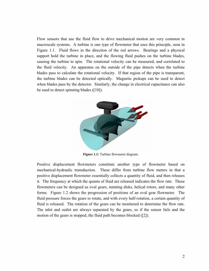
Flow sensors that use the fluid flow to drive mechanical motion are very common in macroscale systems. A turbine is one type of flowmeter that uses this principle, seen in Figure 1.1. Fluid flows in the direction of the red arrows. Bearings and a physical support hold the turbine in place, and the flowing fluid pushes on the turbine blades, causing the turbine to spin. The rotational velocity can be measured, and correlated to the fluid velocity. An apparatus on the outside of the pipe detects when the turbine blades pass to calculate the rotational velocity. If that region of the pipe is transparent, the turbine blades can be detected optically. Magnetic pickups can be used to detect when blades pass by the detector. Similarly, the change in electrical capacitance can also be used to detect spinning blades ([10]).
Figure 1.1: Turbine flowmeter diagram.
Positive displacement flowmeters constitute another type of flowmeter based on mechanical-hydraulic transduction. These differ from turbine flow meters in that a positive displacement flowmeter essentially collects a quantity of fluid, and then releases it. The frequency at which the quanta of fluid are released indicates the flow rate. These flowmeters can be designed as oval gears, nutating disks, helical rotors, and many other forms. Figure 1.2 shows the progression of positions of an oval gear flowmeter. The fluid pressure forces the gears to rotate, and with every half-rotation, a certain quantity of fluid is released. The rotation of the gears can be monitored to determine the flow rate. The inlet and outlet are always separated by the gears, so if the sensor fails and the motion of the gears is stopped, the fluid path becomes blocked ([2]).

3
Figure 1.2: Oval gear positive displacement flowmeter.
At the macroscale, turbines and positive displacement flow meters are usually the most accurate. The high accuracy of positive displacement flowmeters is evident since they control how much fluid flows through them, and eliminate the effects of turbulence in the flow. This accuracy comes at the expense of a very high pressure drop across the sensor. In the oval gear, and similar positive displacement flowmeters, the fluid must force the gears to turn, acting against inertia and friction, from both the gear bearings and the fluid. In the turbine, drag forces on the turbine blades and bearing friction are the cause for a significant pressure drop. At the microscale, these designs, like most devices with moving parts, are very difficult to create. They require the fabrication of complex geometric structures, such as the blades of the turbine, and would typically need to be assembled by bonding parts made on separate wafers. While the accuracy of turbine and positive displacement flowmeters is exemplary, their interference with the flow, and difficulty to fabricate, make them unfeasible for microscale applications. The use of moving parts should be eliminated entirely, which still leaves several flow measurement solutions that can be implemented in both macroscale and microscale applications. Designs such as orifice plates and Venturi nozzles measure the difference in pressure at two points in the fluid channel. For a significant difference in pressure to be observed, the fluid channel must be constricted. These sensors represent a class of flowmeters known as differential pressure flowmeters. Figure 1.3 shows an orifice plate with inlet and outlet pressure taps on either side.
4
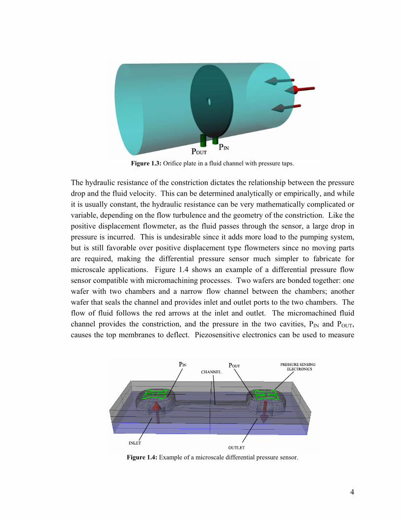
Figure 1.3: Orifice plate in a fluid channel with pressure taps.
The hydraulic resistance of the constriction dictates the relationship between the pressure drop and the fluid velocity. This can be determined analytically or empirically, and while it is usually constant, the hydraulic resistance can be very mathematically complicated or variable, depending on the flow turbulence and the geometry of the constriction. Like the positive displacement flowmeter, as the fluid passes through the sensor, a large drop in pressure is incurred. This is undesirable since it adds more load to the pumping system, but is still favorable over positive displacement type flowmeters since no moving parts are required, making the differential pressure sensor much simpler to fabricate for microscale applications. Figure 1.4 shows an example of a differential pressure flow sensor compatible with micromachining processes. Two wafers are bonded together: one wafer with two chambers and a narrow flow channel between the chambers; another wafer that seals the channel and provides inlet and outlet ports to the two chambers. The flow of fluid follows the red arrows at the inlet and outlet. The micromachined fluid channel provides the constriction, and the pressure in the two cavities, PIN and POUT, causes the top membranes to deflect. Piezosensitive electronics can be used to measure
Figure 1.4: Example of a microscale differential pressure sensor.

5
the membrane deflection and determine the difference in pressure in the two chambers ([4], [5], [9]). In battery-powered microfluidic systems, where low voltage and limited energy are used to drive the pump, the performance can be significantly abated by pumping against a large hydraulic resistance. To avoid such drops in pressure, the use of a sensor that can be integrated into the fluid channel without constriction is essential. Still, many sensor types exist with this attribute. If the fluid is charged, then a sensor utilizing the Lorentz force can be created. In the presence of a magnetic field, charged molecules in the fluid flow experience a force, which can be measured as an electrical voltage, demonstrated in Figure 1.5. Fluid flows in the direction of the red arrows, and the coils on either side of the fluid channel produce a magnetic field in the direction of the green arrows. A voltage proportional to the fluid velocity and magnetic field strength will be detected on electrodes placed perpendicular to the direction of the flow and direction of the magnetic field.
Figure 1.5: Example of an electromagnetic flow sensor.
For neutrally charged fluids, special tracer particles can be introduced into the fluid flow and their motion observed. With a charged tracer particle, the travel time from an emitter to a downstream detector can be measured to determine the fluid velocity. In Laser Doppler Velocimetry and Particle Image Velocimetry, solid tracer particles are introduced into the fluid stream which are detected optically. On large scales, these systems are usually well-refined, but their complexity is difficult to implement at small
6
scales. In drug delivery systems, the introduction of foreign particles into the fluid is not an option, as biocompatibility is a major concern. Instead of injecting particles into the fluid, heat can be injected into the fluid, and the rate at which it is carried away can be used to infer the fluid flow. This type of flow measurement is referred to as thermal anemometry. At the macroscale, hot-wire anemometers consist of a thin strand of metal held in the fluid flow. At the microscale, hot-film anemometers are produced via microfabrication processes, and the device and accompanying electronics can be easily incorporated into the rest of the microfluidic system. Electrical current driven through the wire or film produces heat by Joule heating. The temperature of the sensor can be monitored by its resistance. The rate at which heat is carried away from the wire can be determined, and used to infer the fluid velocity ([1], [3], [7], [8]). The sensor design must also be conscious of the capacity of the power source. For an implantable system, the power source is typically a battery, and it is critical that the power consumption be low. The hot-film anemometer works by driving electrical current through a resistor, so the electronics must be designed to minimize the amount of power used by the sensor. Compared to other sensor systems, where complex, power-consuming electronics would be necessary to optically detect particles or measure the rotation of gears or turbines, a simple, analog circuit would be preferred to control the current through the hot-film anemometer and produce an output voltage representative of the fluid flow. The advantages of the hot-film anemometer in a microscale drug-delivery system outweigh those of other methods. These advantages include:
• simple fabrication and integration into the rest of the pump system • small hydraulic resistance, so the pump is not overloaded • biocompatible, since no foreign particles are introduced into the fluid • slow degradation, since no moving parts are used • control over power-consumption and simple signal-conditioning electronics.
Partly due to their ease of manufacture, thermal anemometers have been in use for several decades. Hot-wire anemometers consist of two probes holding a thin wire in the fluid flow. Therefore, they are simple and versatile enough to be integrated into a variety of different systems. The greatest recent advancement in thermal anemometry is the
7
production of microfabricated devices. The capability of mass production and small size has prompted their use in large scale systems to study turbulence, and in small scale, microfluidic systems. Thermal flow sensing can be accomplished in a few different ways, and thermal anemometry, which requires only a single heating element, has different methods of operation. The options of thermal flow sensing will be investigated and discussed in Chapter 2. To be effective and efficient, the thermal properties of the sensor must be given particular attention. Heat generated contributes to the flow rate signal detected by the sensor, but also accounts for wasted power. The thermal properties can be modified by adjusting the size and shape of the sensor in order to optimize the sensitivity and power consumption, which is investigated in Chapter 3. Finite-element analysis is used in Chapter 4 to model the combination of thermal spreading resistance and fluid flow, and the results can be used to refine the mathematical analysis, eliminating assumptions that may not be accurate in the described application. To determine whether or not fabrication of the sensor at the desired scale is possible is also of critical importance. A unique fabrication process using deposition, lithography, and etching processes in the RIT Semiconductor and Microsystems Fabrication Laboratory is used to build a collection of sensors of various sizes in three different sized fluid channels, described in Chapter 5. To control the sensor heat dissipation, and to generate an electrical signal related to the flow rate, signal conditioning circuitry must be developed, based on the mode of operation of the sensor and thermal properties. Fluctuations in fluid temperature are a major source of error in constant-temperature controlled anemometers, and the circuits presented in Chapter 6 minimize the effect of ambient fluid temperature on circuit output. In order to validate the models and predictions made in Chapters 3 and 4, a means of packaging and testing the sensors fabricated is presented in Chapter 7. Lastly, the results from the mathematical analysis, and simulated performance of the circuits designed in Chapter 6 are combined, and the overall sensor performance evaluated in Chapter 8. REFERENCES
[1] Ashauer, M., et al., “Thermal flow sensor for liquids and gases,” in Micro Electro Mechanical Systems, 1998. MEMS 98. Proceedings., The Eleventh Annual International Workshop on.

8
[2] Baker, R.C., Flow Measurement Handbook. 1 ed. 2000: Cambridge University Press. [3] Baltes, H., O. Paul, and O. Brand, “Micromachined thermally based CMOS
microsensors.” Proceedings of the IEEE, 1998. 86(8): p. 1660-1678. [4] Boillat, M.A., et al., “A differential pressure liquid flow sensor for flow regulation
and dosing systems,” in Micro Electro Mechanical Systems, 1995, MEMS '95, Proceedings. IEEE.
[5] Briand, D., P. Weber, and N.F. de Rooij, “Silicon liquid flow sensor encapsulation using metal to glass anodic bonding,” Micro Electro Mechanical Systems, 2004. 17th IEEE International Conference on. (MEMS) 2004.
[6] Cao, L., S. Mantell, and D. Polla, “Design and simulation of an implantable medical drug delivery system using microelectromechanical systems technology,” Sensors and Actuators A: Physical, 2001. 94(1-2): p. 117-125.
[7] Elwenspoek, M., “Thermal flow micro sensors,” in Semiconductor Conference, 1999. CAS '99 Proceedings. 1999.
[8] Lomas, C.G., Fundamentals of Hot Wire Anemometry, 1986: Cambridge University Press.
[9] Richter, M., et al., “A novel flow sensor with high time resolution based on differential pressure principle,” in Micro Electro Mechanical Systems, 1999. MEMS '99. Twelfth IEEE International Conference on. 1999.
[10] Wadlow, D., “Turbine Flowmeters,” Sensors, 1999. 16(10).

9
THERMAL FLOW MEASUREMENT Thermal anemometers have been in use for several decades, due to their simplicity and ease of manufacture. Thermal anemometers work by creating heat, and monitoring the rate at which it is carried away. In the typical hot-wire anemometer in Figure 2.1, the heating element is simply a thin metal wire. The metal wire generates heat, which is carried away by the moving fluid, in the direction of the red arrows. The rate at which heat is carried away is measured and correlated to the fluid velocity. The supporting posts hold the wire in place in the fluid path ([9]).
Figure 2.1: Basic hot-wire anemometer diagram.
In microfabricated anemometers, the heating element is usually part of a conductive film, and the devices are often referred to as hot-film anemometers. The heat produced raises the temperature of the heating element, and is transferred to the fluid. The amount of heat transferred to the fluid depends on the heater temperature, thermal fluid properties, and fluid velocity. The temperature and electrical resistance of the heating element are related, so the temperature can be determined by monitoring the resistance.

10
I. MODES OF OPERATION All thermal anemometers consist of a resistive heating element held in the fluid as previously described, but there are a variety of methods used to obtain a signal related to the flow velocity. [1] and [4] provide thorough descriptions of the different types, and the associated variations in hardware. These different flow sensor types include calorimeters, anemometers, and time-of-flight sensors. Calorimeters are quite common for flow sensing, and are easy to implement. These require three components: one heating element, and two sensing elements. The sensing elements are placed equidistant from the heater; one upstream and one downstream, seen in Figure 2.2. At a flow rate of zero, the heat dissipates to the two sensing elements equally. When the fluid flows, the sensor downstream will receive more heat, and the sensor upstream, less. As a result, a temperature difference will arise, and a change in resistance can be detected.
Figure 2.2: Calorimeter type flow sensor.
When put into a Wheatstone bridge circuit, the disparity in the amount of heat received from the two sensors can be translated to an imbalance in the legs of the bridge. When the bridge becomes unbalanced, an output voltage can be observed. Therefore, the only electronics needed for a calorimeter are those to drive current through the heater, and a Wheatstone bridge. The major advantage of this type of sensor is that disturbances due to changes in ambient temperature will affect both sensing elements equally, and therefore, the proportionality of elements in the Wheatstone bridge will be unchanged. In
11
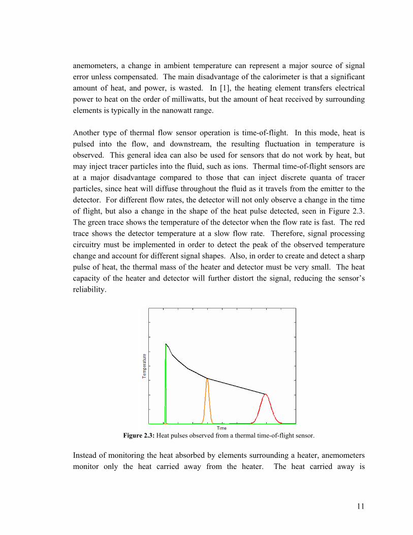
anemometers, a change in ambient temperature can represent a major source of signal error unless compensated. The main disadvantage of the calorimeter is that a significant amount of heat, and power, is wasted. In [1], the heating element transfers electrical power to heat on the order of milliwatts, but the amount of heat received by surrounding elements is typically in the nanowatt range. Another type of thermal flow sensor operation is time-of-flight. In this mode, heat is pulsed into the flow, and downstream, the resulting fluctuation in temperature is observed. This general idea can also be used for sensors that do not work by heat, but may inject tracer particles into the fluid, such as ions. Thermal time-of-flight sensors are at a major disadvantage compared to those that can inject discrete quanta of tracer particles, since heat will diffuse throughout the fluid as it travels from the emitter to the detector. For different flow rates, the detector will not only observe a change in the time of flight, but also a change in the shape of the heat pulse detected, seen in Figure 2.3. The green trace shows the temperature of the detector when the flow rate is fast. The red trace shows the detector temperature at a slow flow rate. Therefore, signal processing circuitry must be implemented in order to detect the peak of the observed temperature change and account for different signal shapes. Also, in order to create and detect a sharp pulse of heat, the thermal mass of the heater and detector must be very small. The heat capacity of the heater and detector will further distort the signal, reducing the sensor’s reliability.
Figure 2.3: Heat pulses observed from a thermal time-of-flight sensor.
Instead of monitoring the heat absorbed by elements surrounding a heater, anemometers monitor only the heat carried away from the heater. The heat carried away is

12
proportional to the equivalent thermal conductance of the fluid, which is related to the flow rate. This is slightly more complicated, since the accompanying electronics must determine how much heat is actually carried away by the fluid, and how much heat is absorbed by the sensor. Rarely are both of these values actually determined, but instead, the amount of heat that the heater produces is carefully controlled. The two primary control methods are constant-power anemometry, and constant-temperature anemometry ([10]). In constant-power anemometry, current is driven through the heating element so that the power dissipated is invariant. The heater temperature will rise and settle, so that at steady state, all of the power consumed is dissipated as heat to the fluid and to connecting hardware. When the fluid flow changes, the heater temperature will rise or fall to a new steady-state temperature. The temperature is monitored via the heater resistance to determine the flow rate. The thermal time constant is dependent on the heat capacity of the sensor, its mass, and the thermal resistance, and determines the frequency response of the anemometer in constant-power mode. Therefore, a heater with less mass will respond faster to changes in flow rate ([8]). In constant-temperature mode, the power dissipated by the sensor is controlled so that the heater temperature does not change. Therefore, when the fluid flows faster and the thermal conductance increases, the sensor dissipates more heat. Since the heater temperature does not change, the thermal time constant does not exclusively determine the sensor frequency response. Instead, the speed of response is dictated by the electronics, which operate much faster than changes in the thermal domain. In both modes of anemometer operation, the sensor is dependent on changes in ambient temperature. Therefore, a compensation circuit is usually necessary, along with an additional sensing resistor to detect the ambient temperature ([5]). The resistance of the ambient temperature sensor can be used to determine the ambient temperature, and can modulate the output signal appropriately. The difficulty here is that in order to measure the resistance, the voltage response to current, or vice versa, must be measured. Therefore, the ambient temperature sensor must dissipate power and will self-heat. While the heating resistor is optimized to self-heat, self-heating in the ambient temperature sensor leads to error in the signal. This can be minimized, but is ultimately unavoidable.
13
Since the constant-temperature anemometer mode of operation has the fastest transient response, this mode of operation will be investigated further. The associated assumptions (i.e. change in heater temperature equal to zero) will be included in the mathematical analysis. The control circuit in Chapter 6 will be designed to maintain the heater at a constant temperature.
II. SENSOR DESIGN Microfabricated thermal anemometers date back to the early 1970’s ([14]). In [13], the heat transfer and signal-conditioning circuitry are discussed for a silicon-based thermal anemometer. The sensor presented is intended for gas flows, and has an area of about two square millimeters, but the same principles are used in smaller and more advanced thermal anemometers developed recently. Many make use of doped polysilicon as heating elements mounted on a silicon substrate, with slight changes in the fabrication process to address issues such as power lost to the substrate and slow thermal response. There are a number of factors to take into account when optimizing the design of the sensor. The most critical design factor must be to ensure that an excessive amount of heat is not dissipated to the substrate of the sensor (i.e. the sensor must be thermally isolated). If designing the sensor to run off a battery, this is especially important since heat dissipated to the substrate constitutes wasted power. Another design feature to give attention to is to maximize the sensitivity of the sensor. The sensitivity is primarily dependent on the thermal conductance to the fluid. However, maximizing the conductance does not necessarily maximize the sensitivity. Therefore, particular consideration to the size and shape of the heating element should be given. In microfabricated flow sensors, the layout and fabrication process can be designed to optimize the power efficiency and sensitivity of the sensor. One of the first and simplest designs for a thermal anemometer is described in [12]. Two resistors are created with a platinum film, which sit on a silicon wafer and a layer of silicon nitride for thermal isolation. One of the resistors serves as a sensor for fluid temperature, and the other is heated and used to measure the fluid flow. The silicon is etched away on the back side of the sensors so that they rest on a thin silicon membrane, which is also done in [7]. The large thermal resistance of the membrane will reduce the heat lost to the bulk substrate.
14
Compared to other materials, silicon acts as thermal conductor. Its thermal conductivity is approximately half as much as many metals (gold, copper, silver), but over 100 times that of silicon dioxide. In [11], the issue of thermal isolation is specifically addressed. Stemme, in [11], presents a silicon thermal anemometer for gas flows, where the device is initially built on silicon, but its structural connection to the substrate is replaced by polyimide, a polymer with much lower thermal conductivity than silicon which behaves as a thermal insulator. The sensor in [11] is fabricated on a silicon wafer, but is designed separately from the fluid channel, and must be inserted. For totally microfluidic systems, all the components should be integrated, so no assembly is required. [11] also discusses the thermal mass of the sensor. Having a small thermal mass improves the frequency response and the sensitivity of the sensor. A comparison of the sensor with the polyimide support to a sensor with a silicon support shows that the power necessary to hold the sensor at a constant temperature is approximately half as much, and the sensitivity is improved. When a step response is applied to the two sensors, the sensor with a polyimide bridge rises and settles in under a second, whereas the sensor with a purely silicon support takes almost 5 seconds to settle. In [3], the integration of a thermal flow sensor into a microfluidic system is discussed. Instead of measuring the change in thermal conductance versus flow rate, the sensor in [3] measures the time it takes for a heat pulse generated by a heater to reach a detector. The fluid channel is created by etching one side of a silicon wafer, with the heating and detecting elements on the opposite side. A glass wafer with an inlet and outlet port is bonded to the silicon wafer. Therefore, the fluid flows across one side of the heating and detecting elements. Because this particular sensor works off time-of-flight and not thermal conductance, the sensitivity is not affected by the thermal conductance to the substrate, aside from the shape of the heat pulse. A comparison of time-of-flight sensors, anemometers, and calorimeters is discussed in [1]. For hot-film anemometers that depend on the thermal conductance to the fluid, having the fluid flow across both sides of the sensor improves the sensitivity. For fluid to flow on both sides of a surface micromachined sensor, the fluid channel would need to be etched into the wafer underneath the sensor and bonded to another etched wafer. A liquid dosing system described in [6] contains a thermo-pneumatic pump, thermal flow sensor, and a pair of check valves, all manufactured on a single wafer. The flow sensor is surface micromachined with gold resistors on top of a silicon nitride support layer. The
15
silicon beneath the silicon nitride is etched, and the wafer is bonded to an etched Pyrex wafer to create the flow channel. This particular sensor is a calorimeter style flow sensor, which has a sensing element upstream and downstream from a heater. In many systems, it is undesirable to bond many wafers together to create microchannels and cavities. With CMOS technology dominating microelectronics, considerable research has been done integrate microfluidics into CMOS processing. In [2], the integration of mechanical sensors into CMOS devices with bulk and surface micromachining is discussed. The use of a sacrificial layer is introduced, which allows for a structure, such as an anemometer bridge, to be built on top, and the sacrificial layer etched away afterwards. Silicon dioxide and aluminum are recommended as sacrificial materials for CMOS sensors. However, if films that require high-temperatures, such as polysilicon or silicon nitride, are to be deposited, aluminum is not an option. For bulk micromachining of silicon, potassium hydroxide is recommended, which produces an etch selective to silicon, and is anisotropic based on crystal orientation. In [15], an anemometer is fabricated in a CMOS system, after the processing of the CMOS devices. Holes, which also serve as vias for metal layers, are etched to provide a pathway for etchant solution to the silicon substrate. Protecting the CMOS devices from the etchant solution is very important, since the anemometer in [15] is designed to improve the low yield achieved with a previous fabrication process. Process steps with high selectivity are typically needed when trying to etch a microchannel while not destroying already existing devices on the chip. In [2], this is accomplished with KOH etching, and in [15], a xenon difluoride dry etch etches silicon but not other materials. From past results of micromachined thermal anemometers, characteristics of an ideal sensor can be determined:
• thermal isolation from the substrate • small thermal mass • heat dissipation to the center of the fluid channel • simple integration with the rest of the microfluidic system • micromachining process that does not damage existing structures on the device.
To meet these design characteristics, a sensor bridge could be fabricated to stretch across the flow channel. Bridges can be created on top of a sacrificial layer, so that etching the sacrificial layer releases the bridge, and the fluid channel is etched into wafer underneath.

16
Two wafers with half of the flow channel etched in each can be bonded together so that the bridge sits in the middle of the channel, distributing heat to both halves. By concentrating the heat generation in the center of the fluid channel, and away from the channel walls, the amount lost to the substrate can be minimized. The fluid velocity in the center of the channel should be greatest, so the sensitivity will also be maximized. The heating element of the bridge can be created with doped polysilicon. To protect the doped polysilicon during the etching of the silicon fluid channel, another material, such as silicon oxide or silicon nitride, can be used to encapsulate the doped polysilicon. Figure 2.4 shows a diagram of the solution described. Half of the fluid channel is formed in the bottom, silicon wafer, and the other half is formed in a glass wafer. A surfaced micromachined sensor on the silicon wafer would then sit in the center of the fluid channel. The sensor bridge is made of conductive polysilicon, encapsulated in silicon nitride, which will robustly withstand the silicon etch to form the fluid channel. Having the bridge narrow in the center, and tapered out to attach to the channel walls concentrates the heat generation near the center since the width is reduced, and resistance per length increased. The tapered attachments offer some thermal isolation, but because they must be formed from materials with high thermal conductivities, the amount of isolation will vary depending on the size and shape of the sensor. The sensor is formed by films on the order of hundreds of nanometers thick, so the volume, and therefore the mass, will be very small. The small mass translates to a small heat capacity, so the thermal response should be very fast.
Figure 2.4: Example of a thermal anemometer in a fluid channel made from a silicon wafer and glass
wafer.

17
Detailed thermal properties of this sensor design will be investigated in following chapters. In general, a larger heater area improves the sensitivity, but also increases the amount of wasted power. Making the sensor narrower will decrease the wasted power, but also decrease the sensitivity. Due to these competing performance parameters, the tradeoff between power and sensitivity should be analyzed. Then, the amount of power necessary to produce the minimum sensitivity required, without exceeding the maximum temperature permissible, may be determined. Lithographic resolution will determine the limit on how narrow a sensor may be fabricated, although very narrow sensors may not be durable enough to withstand the entire fabrication process. Therefore, sensors of various sizes and shapes will be fabricated to determine robustness. REFERENCES
[1] Ashauer, M., et al., “Thermal flow sensor for liquids and gases,” in Micro Electro Mechanical Systems, 1998. MEMS 98. Proceedings., The Eleventh Annual International Workshop on. 1998.
[2] Baltes, H., O. Paul, and O. Brand, “Micromachined thermally based CMOS microsensors,” Proceedings of the IEEE, 1998. 86(8): p. 1660-1678.
[3] Branebjerg, J., et al., “A micromachined flow sensor for measuring small liquid flows” Solid-State Sensors and Actuators, 1991. Digest of Technical Papers, TRANSDUCERS '91., 1991 International Conference on. 1991.
[4] Elwenspoek, M., “Thermal flow micro sensors,” in Semiconductor Conference, 1999. CAS '99 Proceedings. 1999.
[5] Fujita, H., et al., “A thermistor anemometer for low-flow-rate measurements,” Instrumentation and Measurement, IEEE Transactions on, 1995. 44(3): p. 779-782.
[6] Lammerink, T.S.J., M. Elwenspoek, and J.H.J. Fluitman., “Integrated micro-liquid dosing system,” in Micro Electro Mechanical Systems, 1993, MEMS '93, Proceedings An Investigation of Micro Structures, Sensors, Actuators, Machines and Systems. IEEE. 1993.
[7] Mailly, F., et al., “Anemometer with hot platinum thin film,” Sensors and Actuators A: Physical, 2001. 94(1-2): p. 32-38.
[8] Makinwa, K.A.A. and J.H. Huijsing, “Constant power operation of a two-dimensional flow sensor,” Instrumentation and Measurement, IEEE Transactions on, 2002. 51(4): p. 840-844.

18
[9] Mischler, M., et al., “A micro silicon hot-wire anemometer,” in Microelectronics and VLSI, 1995. TENCON '95., IEEE Region 10 International Conference on.
[10] Rasmussen, A. and M.E. Zaghloul, “The design and fabrication of microfluidic flow sensors,” in Circuits and Systems, 1999. ISCAS '99. Proceedings of the 1999 IEEE International Symposium on. 1999.
[11] Stemme, G.N., “A monolithic gas flow sensor with polyimide as thermal insulator,” Electron Devices, IEEE Transactions on, 1986. 33(10): p. 1470-1474.
[12] Tabata, O., “Fast-response silicon flow sensor with an on-chip fluid temperature sensing element,” Electron Devices, IEEE Transactions on, 1986. 33(3): p. 361-365.
[13] van Putten, A.F.P., “An integrated silicon anemometer,” in Solid State and Smart Sensors, IEE Colloquium on. 1988.
[14] van Putten, A.F.P., S. Middelhoek, “Integrated silicon anemometer”, Electron. Lett. 10 (1974) 425-426
[15] Yu-Jen, F., et al., “Commercialized CMOS Compatible Micro Anemometer,” in Sensors, 2006. 5th IEEE Conference on. 2006.
19
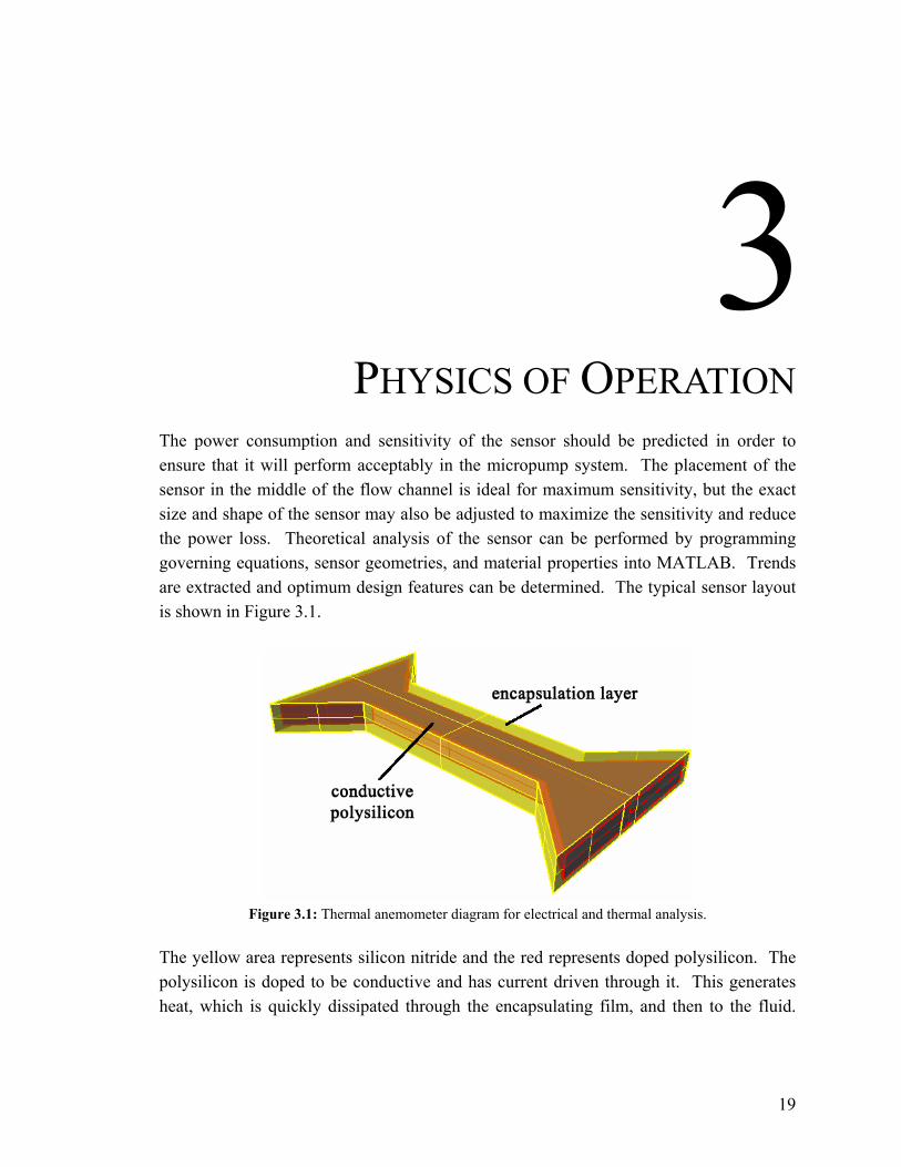
PHYSICS OF OPERATION The power consumption and sensitivity of the sensor should be predicted in order to ensure that it will perform acceptably in the micropump system. The placement of the sensor in the middle of the flow channel is ideal for maximum sensitivity, but the exact size and shape of the sensor may also be adjusted to maximize the sensitivity and reduce the power loss. Theoretical analysis of the sensor can be performed by programming governing equations, sensor geometries, and material properties into MATLAB. Trends are extracted and optimum design features can be determined. The typical sensor layout is shown in Figure 3.1.
Figure 3.1: Thermal anemometer diagram for electrical and thermal analysis.
The yellow area represents silicon nitride and the red represents doped polysilicon. The polysilicon is doped to be conductive and has current driven through it. This generates heat, which is quickly dissipated through the encapsulating film, and then to the fluid.

20
The silicon nitride serves to electrically isolate the polysilicon from the fluid, and is also necessary for fabrication to be possible. The region in the center of the channel where the sensor narrows is where heat generation is most dense. The connections to the channel walls are tapered, which increases the cross-sectional area of the polysilicon, decreasing the resistivity per length, and thus, decreasing heat generated. The larger cross-sectional area also decreases the thermal resistance per length, which would cause more heat to be last to the substrate, but the distance from the region of concentrated heat generation to the channel wall is also increased. The diagram in Figure 3.2 shows the geometric variables used in the electrical and thermal analysis of the sensor. A description of each is also given in Table 3.1.
Figure 3.2: Diagram of geometric variables.
Table 3.1: Sensor Geometry Parameters
CW channel width LE length of polysilicon at narrow region WE width of polysilicon at narrow region tE polysilicon thickness LT length of nitride at narrow region WT width of nitride at narrow region tT thickness used in thermal analysis

21
I. ELECTRICAL DOMAIN The equivalent model for electrical analysis is shown in Figure 3.3. Voltage is applied at the two ends of the sensor, and current, IHEATER, flows. Most of the resistance of the polysilicon is in the center of the channel where the cross-sectional area is small, labeled Rheater. The value of Rheater is computed using equation (3.1), where ρE is the resistivity, and LE, WE, and tE are shown in Figure 3.2.
Figure 3.3: Electrical domain diagram.
EE
EEheater tW
LR⋅
= ρ (3.1)
The tapered areas have a smaller resistance, labeled Rattach, which is computed using (3.2). The variable of integration, x, is the distance from the end of the narrow section of the sensor to the channel wall. The substitution of W(x) with WE+2x is only valid in this design, where the taper angle of the attachment is 45°.
( )⎥⎦
⎤⎢⎣
⎡−⎟⎟
⎠
⎞⎜⎜⎝
⎛⎟⎠⎞
⎜⎝⎛ −
+=⋅+
=⋅
= ∫∫−
=
−
=E
EE
E
ELCW
x EEE
LCW
x EEattach W
LCWW
ttxWdx
txWdxR
EE
ln2
2ln2)2()(
2/)(
0
2/)(
0
ρρρ
⎟⎟⎠
⎞⎜⎜⎝
⎛−+=
E
E
EE
Eattach W
LWCW
tR 1ln
2ρ
(3.2)
The following example shows the normalized distribution of resistance in a sensor in a 100 µm diameter fluid channel, with length, LE, of 60 µm and width, WE, of 6 µm. Since the resistance is inversely proportional to width, the resistance drops sharply at the

22
transition from the straight region to the tapered region. This forces the heat generation to be concentrated in the middle of the sensor.
0 10 20 30 40 50 60 70 80 90 1000.1
0.2
0.3
0.4
0.5
0.6
0.7
0.8
0.9
1
Channel Distance (um)
Polysilicon WidthResistance per Length
Figure 3.4: Electrical characteristics vs. distance from channel wall for typical anemometer geometry.
Most materials, polysilicon included, exhibit a change in resistance with a change in temperature. The relationship is characterized by a polynomial relationship, as in (3.3). Typically, only the first order term, α0, is significant, especially over small changes in temperature. It is due to this effect that the ambient temperature sensor, which will be minimally self-heated, can be used to determine the ambient temperature. ...))()(1( 2
01000 +−+−+= TTTTRR αα (3.3) The resistive bridge serves as a transducer of electrical power to heat, which is then dissipated to the fluid. The power dissipated by the sensor is calculated by (3.4).
( )
attachheaterattachheaterheaterelectrical RR
VVRRIP
2)2(
22
+−
=+= −+ (3.4)

23
The power dissipated is directly proportional to the resistance, and by combining (3.1) and (3.2), the percent of the total power dissipated by narrow region of the sensor, P%, is calculated by (3.5).
1001ln
⋅
⎟⎟⎠
⎞⎜⎜⎝
⎛−++
=
E
E
EE
E
E
E
%
WL
WCW
WL
WL
P (3.5)
II. THERMAL DOMAIN Calculations for the thermal properties of the sensor are similar to the calculations of the electrical characteristics, since the tapered attachments to the channel wall act as thermal resistances, and account for conduction to the substrate of the device. Convection to the fluid also acts as a thermal resistance, and is dependent on the fluid properties and fluid velocity. Heat is transferred by three basic methods: conduction, convection, and radiation. The generic case of thermal conduction is through a single material or substance, of length, L, and cross-sectional area, ACS, shown in Figure 3.5.
Figure 3.5: Diagram of heat conduction.
The rate of heat transfer, Q, by conduction is calculated in (3.6), and is proportional to the difference in temperature across the volume, T2-T1. The definition of variables and constants in (3.6), and in all heat transfer equations, are summarized in Table 3.2.

24
)( 12 TTL
kAQ CScond −= . (3.6)
The process of convection constitutes heat transfer from a solid to a fluid. Since the molecules of fluid are constantly moving and transferring heat much more randomly than in a solid, the only significant geometry factor affecting convective heat transfer, in (3.7), is the area of the boundary between the two bodies, Aconv. )( fluidsolidconvconv TThAQ −= (3.7) Since heat transfer between solids and fluids is dependent on a number of factors, such as thermal conductivities, viscosity, and fluid motion, purely mathematical prediction of the convection coefficient, h, is unreliable, and usually must be determined by experiment or simulation. Heat transfer by radiation represents heat loss similar to when a burner glows red. Heat energy is removed from the system in the form of photonic energy, and is characterized by (3.8). )( 44
ambientsolidradrad TTAeQ −= σ . (3.8) In the analysis of this system, the thermal radiation term is negligible, since the overheat temperature of the sensor will only be on the order of 100 to 102 degrees Kelvin, making the energy lost to radiation on the order of picowatts. The dominant heat transfer effects will be on the order or milliwatts and microwatts. If the sensor temperature were approaching a few hundred degrees above ambient, then the thermal radiation may significant. The last major effect to take into account is what happens when heat is absorbed by an object. Obviously, the temperature rises, but the increase in temperature is dependent on the properties of the material being heated, seen in (3.9).
dt
dTcVQ solid
mstored ρ= (3.9)
25
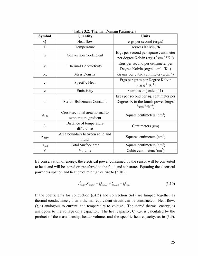
Table 3.2: Thermal Domain Parameters Symbol Quantity Units
Q Heat flow ergs per second (erg/s) T Temperature Degrees Kelvin, ºK
h Convection Coefficient Ergs per second per square centimeter per degree Kelvin (erg·s-1·cm-2·°K-1)
k Thermal Conductivity Ergs per second per centimeter per Degree Kelvin (erg·s-1·cm-1·ºK-1)
ρm Mass Density Grams per cubic centimeter (g·cm-3)
c Specific Heat Ergs per gram per Degree Kelvin
(erg·g-1·ºK-1) e Emissivity <unitless> (scale of 1)
σ Stefan-Boltzmann Constant Ergs per second per sq. centimeter per Degrees K to the fourth power (erg·s-
1·cm-2·ºK-4)
ACS Cross-sectional area normal to
temperature gradient Square centimeters (cm2)
L Distance of temperature
difference Centimeters (cm)
Aconv Area boundary between solid and
fluid Square centimeters (cm2)
Arad Total Surface area Square centimeters (cm2) V Volume Cubic centimeters (cm3)
By conservation of energy, the electrical power consumed by the sensor will be converted to heat, and will be stored or transferred to the fluid and substrate. Equating the electrical power dissipation and heat production gives rise to (3.10). convcondstoredheaterheater QQQRI ++=2 (3.10) If the coefficients for conduction (kA/L) and convection (hA) are lumped together as thermal conductances, then a thermal equivalent circuit can be constructed. Heat flow, Q, is analogous to current, and temperature to voltage. The stored thermal energy, is analogous to the voltage on a capacitor. The heat capacity, CHEAT, is calculated by the product of the mass density, heater volume, and the specific heat capacity, as in (3.9).
26
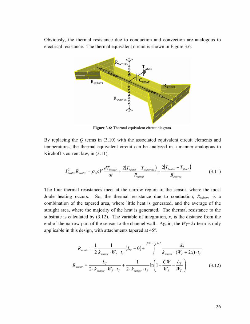
Obviously, the thermal resistance due to conduction and convection are analogous to electrical resistance. The thermal equivalent circuit is shown in Figure 3.6.
Figure 3.6: Thermal equivalent circuit diagram.
By replacing the Q terms in (3.10) with the associated equivalent circuit elements and temperatures, the thermal equivalent circuit can be analyzed in a manner analogous to Kirchoff’s current law, in (3.11).
( ) ( )
convec
fluidheater
substr
substrateheaterheatermheaterheater R
TTR
TTdt
dTcVRI−
+−
+=222 ρ (3.11)
The four thermal resistances meet at the narrow region of the sensor, where the most Joule heating occurs. So, the thermal resistance due to conduction, Rsubstr, is a combination of the tapered area, where little heat is generated, and the average of the straight area, where the majority of the heat is generated. The thermal resistance to the substrate is calculated by (3.12). The variable of integration, x, is the distance from the end of the narrow part of the sensor to the channel wall. Again, the WT+2x term is only applicable in this design, with attachments tapered at 45°.
( ) ∫−
⋅+⋅+−
⋅⋅=
2/)(
0 )2(01
21 TLCW
TTsensorT
TTsensorsubstr txWk
dxLtWk
R
⎟⎟⎠
⎞⎜⎜⎝
⎛−+
⋅⋅+
⋅⋅⋅=
T
T
TTsensorTTsensor
Tsubstr W
LWCW
tktWkL
R 1ln2
12
(3.12)
27
The expression for Rconvec is significantly more complex, since it represents the spreading resistance to a fluid. The spreading resistance to an infinite half-space from a rectangle is described in (3.13) ([4]).
( )⎥⎥⎥
⎦
⎤
⎢⎢⎢
⎣
⎡
⎟⎟⎟
⎠
⎞
⎜⎜⎜
⎝
⎛
⎟⎟⎠
⎞⎜⎜⎝
⎛+−+++⎟⎟
⎠
⎞⎜⎜⎝
⎛= −−
23
2311
01111
3sinh11sinh
ζζζζ
ζζπζ
Tfluidconvec Ak
R (3.13)
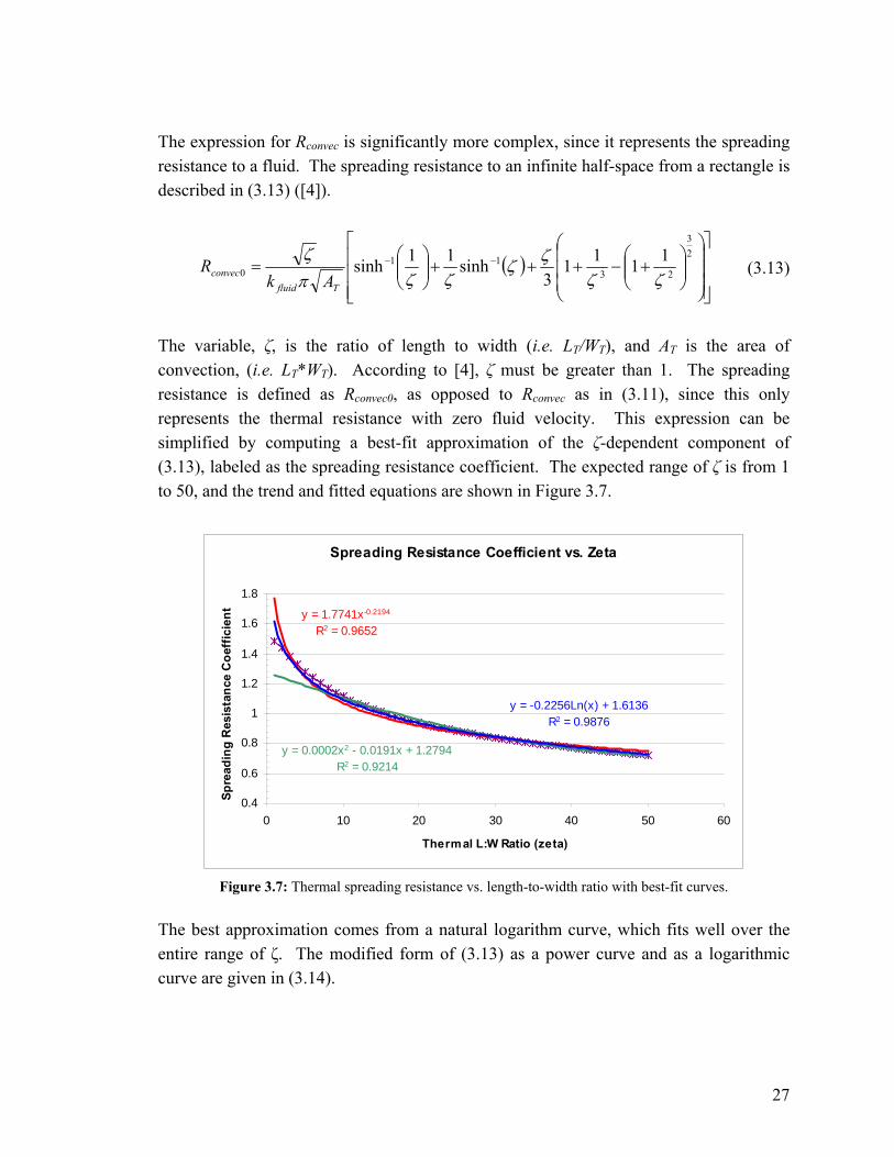
The variable, ζ, is the ratio of length to width (i.e. LT/WT), and AT is the area of convection, (i.e. LT*WT). According to [4], ζ must be greater than 1. The spreading resistance is defined as Rconvec0, as opposed to Rconvec as in (3.11), since this only represents the thermal resistance with zero fluid velocity. This expression can be simplified by computing a best-fit approximation of the ζ-dependent component of (3.13), labeled as the spreading resistance coefficient. The expected range of ζ is from 1 to 50, and the trend and fitted equations are shown in Figure 3.7.
Spreading Resistance Coefficient vs. Zeta
y = 1.7741x-0.2194
R2 = 0.9652
y = 0.0002x2 - 0.0191x + 1.2794R2 = 0.9214
y = -0.2256Ln(x) + 1.6136R2 = 0.9876
0.4
0.6
0.8
1
1.2
1.4
1.6
1.8
0 10 20 30 40 50 60
Thermal L:W Ratio (zeta)
Spre
adin
g R
esis
tanc
e C
oeff
icie
nt
Figure 3.7: Thermal spreading resistance vs. length-to-width ratio with best-fit curves.
The best approximation comes from a natural logarithm curve, which fits well over the entire range of ζ. The modified form of (3.13) as a power curve and as a logarithmic curve are given in (3.14).

28
( )( )ζπ
ζπ
ln226.0614.11774.11 219.00 −≈≈ −
TfluidTfluidconvec AkAk
R (3.14)
None of these approximations hold when the length-to-width ratio is less than 1. Since the relationship should be logarithmically symmetric about the value 1, (i.e.: the same results should be obtained for 1/2 as for 2, and 1/10 as for 10), a complete fitted trend may be found as a function of the logarithm of ζ. On a logarithmic scale, the log of 1/ζ and the log of ζ will have the same displacement from the point of symmetry. The plot of the thermal spreading resistance according to (3.13), with ζ greater than 1 and less than 1, and the best-fit curves are shown in Figure 3.8.
Spreading Resistance Coefficient vs. Zeta
y = -0.2414x2 - 7E-16x + 1.3793R2 = 0.9766
y = 0.0478x4 + 7E-14x3 - 0.3936x2 - 2E-12x + 1.4679R2 = 0.9994
0.4
0.6
0.8
1
1.2
1.4
1.6
1.8
-2 -1.5 -1 -0.5 0 0.5 1 1.5 2
Log (Thermal L:W Ratio (zeta))
Spre
adin
g R
esis
tanc
e C
oeff
icie
nt
Figure 3.8: Spreading resistance vs. logarithm of the length-to-width ratio.
A parabolic fit is shown in orange in Figure 3.8, and a quartic trend is shown in green. The quartic trendline fits the data with an R2 value over 99.9%. Since the data is symmetric about 0, the coefficients of the even exponents are the only ones that are significant. The quartic function will be much easier to modify than (3.13) when incorporating the change due to fluid flow. To take into account the fluid velocity, the Nusselt number is incorporated into the thermal resistance expression. This number represents the ratio of convective heat transfer to conductive heat transfer. In [2], the Nusselt number for forced convection

29
over surfaces is shown to be related to the Reynolds number, (3.15), and the Prandtl number, (3.16), by (3.17).
μρ Lu ⋅⋅
=Re (3.15)
k
cp μ⋅=Pr
(3.16)
2/13/1 RePr664.0Nu ⋅⋅= (3.17) The variables for fluid properties in (3.15), (3.16), and (3.17) are summarized in Table 3.3.
Table 3.3: Fluid Property Variables Symbol Quantity Units
ρ Density Grams per cubic centimeter (g·cm-3)μ Viscosity Poise (g·cm-1·s-1) u Fluid Velocity Centimeters per second (cm·s-1) L Characteristic Length Centimeters (cm)
cp Specific Heat Capacity Ergs per gram per degree Kelvin
(erg·g-1·ºK-1)
k Thermal Conductivity Ergs per second per centimeter per Degree Kelvin (erg·s-1·cm-1·ºK-1)
h Convection Coefficient Ergs per second per square
centimeter per degree Kelvin (erg·s-1·cm-2·°K-1)
To include the effect of fluid velocity, the Rconvec term in (3.11) is calculated by (3.18).
Nu1
0
+= convec
convecRR (3.18)
For the thermal analysis, it will be more intuitive to consider thermal conductances than thermal resistances. Since conductance is simply the inverse of resistance, Rconvec in (3.18) becomes Gconvec, shown in (3.19). ( )Nu10 += convecconvec GG (3.19)

30
To isolate the dependence on fluid velocity, a parameter, F, is introduced in (3.20) to combine the thermal and fluidic constants in (3.17).
2/13/1
664.0Nu⎟⎟⎠
⎞⎜⎜⎝
⎛ ⋅⋅⎟⎟
⎠
⎞⎜⎜⎝
⎛ ⋅⋅=≡
μρμ L
kc
uF p (3.20)
If (3.19) is modified to include F, then the expression for Gconvec in (3.21) is obtained. ( )uFGG convecconvec += 10 . (3.21) This result shows a square-root dependence of convection on fluid velocity, used in many representations of King’s Law. The general form of King’s Law is χbuah += , or ( )χβuGG convecconvec += 10 . (3.22) The variable h is the coefficient in convective heat transfer. The variables a, b, and χ, are curve fitting parameters which are most reliably determined by experiment. The exponent, χ, is often cited to be approximately one-half, which is consistent with the expression of the Nusselt number, implemented in (3.21). In (3.22) with χ equal to one half, β is equivalent to F. When King’s Law is fitted to experimental data in later chapters, this may not necessarily be true, so β should not be defined as equal to F. With the dependence of thermal convection on fluid velocity estimated, (3.11) and (3.21) can be combined into (3.23).
( ) ( )( )uFTTGTTGdt
dTcVRI fluidheaterconvecsubstrateheatersubstrheater
mheaterheater +−+−+= 122 02 ρ
(3.23) The sensor control electronics will be designed so that the sensor is held at a constant temperature. Therefore, in balancing the electrical and thermal energy transfer, no change in electrical resistance due to temperature should need to be taken into account, and the energy stored due to heat capacity should be constant. With Qstored equal to zero, (3.23) becomes (3.24).
( ) ( ) ( )uFTTGTTGRI fluidheaterconvecsubstrateheatersubstrheaterheater +⋅−⋅⋅+−⋅⋅= 122 02 (3.24)

31
Typically, the fluid and substrate will be at the same temperature, and the heater will be driven to a fixed overheat temperature above the fluid temperature, defined as TOH. If the difference in heater temperature and fluid temperature is replaced with TOH, the thermal conductances can be combined into a total thermal conductance, Gtotal, in (3.25). ( )uFGGG convecsubstrtotal +⋅+⋅= 122 0 (3.25) If the electrical power is computed by the voltage across the narrow part of the sensor, Vheater, instead of the current, and TOH is incorporated, (3.24) can be modified to (3.26).
( ) ( ) ( )uFTGTGPRV
OHconvecOHsubstrheater
heater +⋅⋅⋅+⋅⋅== 122 0
2
(3.26)
From (3.26), the sensitivity, S, of the heater voltage, Vheater, to fluid velocity, u, can be determined. The derivatives of total conductance to fluid velocity, power to total conductance, and heater voltage to power are calculated in (3.27), (3.28), and (3.29).
u
FGdu
dG convectotal 0= (3.27)
OHtotal
TdG
dP= (3.28)
totalOH
heaterheaterheater
GTR
PR
dPdV
22== (3.29)
Combining (3.27), (3.28), and (3.29) yields the total sensitivity, in (3.30).
u
FGG
TRdu
dVS convec
total
OHheaterheater 0
2== (3.30)
As seen from (3.30), the sensitivity can be maximized by increasing the percent of the total conductance that is convection. The overheat temperature can also be increased to improve the sensitivity, but there may be limits on allowable temperatures. The

32
sensitivity and power tradeoff due to sensor geometry and overheat temperature can be analyzed in detail using MATLAB.
III. MATLAB ANALYSIS With the governing equations presented, MATLAB will be used to vary the dimensions of the sensor, and observe the resulting changes in thermal conductances. A high value of conductance due to convection will indicate a high sensitivity, but the total conductance is proportional to the power consumption. The values in Table 3.4 will be used as default values in analyses in which only one variable is swept, unless otherwise specified. The MATLAB scripts used for calculations and varying parameters are in Appendix A.
Table 3.4: Nominal Sensor Parameters in MATLAB Simulations Variable Value Units
CW 100 µm LT 50 µm WT 8 µm tT 900 nm LE 50 µm WE 2 µm tE 600 nm U 75 nL/min
TOH 10 ºK With the default sensor parameters, the following trends versus flow rate are obtained. As dictated by the thermal conductance expression in (3.21), the thermal conductance increases with a square-root dependence on fluid velocity, seen in Figure 3.9. Therefore, the power necessary to hold the sensor at the desired overheat temperature increases, along with the voltage. The power dissipation versus flow rate is shown in Figure 3.10, and follows the same shape as the Figure 3.9. The thermal conductance in Figure 3.9 and power in Figure 3.10 are given in centimeter-gram-second (CGS) units. A table listing the units associated with different quantities (e.g. force, energy, pressure) in CGS units and conversions to standard units is included in Appendix C.
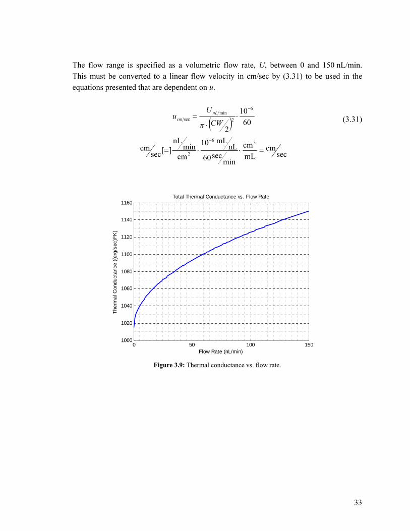
33
The flow range is specified as a volumetric flow rate, U, between 0 and 150 nL/min. This must be converted to a linear flow velocity in cm/sec by (3.31) to be used in the equations presented that are dependent on u.
( ) 6010
2
6
2min
sec
−
⋅⋅
=CW
Uu nL
cmπ
(3.31)
seccm
mLcm
minsec60
nLmL10
cmmin
nL][sec
cm36
2 =⋅⋅=−
0 50 100 1501000
1020
1040
1060
1080
1100
1120
1140
1160
Flow Rate (nL/min)
Ther
mal
Con
duct
ance
((er
g/se
c)/ °K
)
Total Thermal Conductance vs. Flow Rate
Figure 3.9: Thermal conductance vs. flow rate.

34
0 50 100 1501
1.02
1.04
1.06
1.08
1.1
1.12
1.14
1.16x 10⁴
Flow Rate (nL/min)
Pow
er D
issi
pate
d (e
rg/s
ec)
Power Dissipation vs. Flow Rate
0 50 100 1501
1.02
1.04
1.06
1.08
1.1
1.12
1.14
1.16
Pow
er D
issi
pate
d (m
W)
Figure 3.10: Anemometer power dissipation vs. flow rate.
The output voltage necessary to produce the power in Figure 3.10 is shown in Figure 3.11. The trend is similar but not the same, since the thermal conductance is directly proportional to the power, but the voltage is directly related to the square-root of the power.
0 50 100 1501.6
1.62
1.64
1.66
1.68
1.7
1.72
1.74
Flow Rate (nL/min)
Vol
tage
(V)
Output Voltage vs. Flow Rate
Figure 3.11: Anemometer voltage vs. flow rate.

35
These initial results are reassuring in that the thermal conductance varies significantly (close to 10% across the full range) as the flow rate changes. The power consumption to produce a 10°K overheat temperature is approximately 1 mW, and the voltage necessary is low enough to be generated by a battery. As expected from the (3.13) and Figure 3.7, a larger heater area and greater length-to-width ratio should produce a sensor with smaller thermal resistance. Since the fluid flow sensitivity is proportional to the heater’s thermal conductance, it would be beneficial to minimize the thermal resistance of the heater. Since changing the heater’s length and width also affects the thermal resistance to the substrate, there is a tradeoff established between sensitivity of the sensor, and heat and power lost to the substrate. The thermal length-to-width ratio of the sensor has a complicated relationship with the thermal spreading resistance, which can be approximated with a logarithmic trend. When the heater geometry is modified to vary this ratio while keeping the heater area constant, the trends of thermal conductance due to conduction lost to the substrate and convection to the fluid in Figure 3.12 are obtained. With the area and length-to-width ratio being controlled, the length, LT, and width, WT, used in the calculations for thermal conductances must be calculated using (3.32) and (3.33).
ζ
TT
AW = (3.32)
ζTT AL = (3.33)
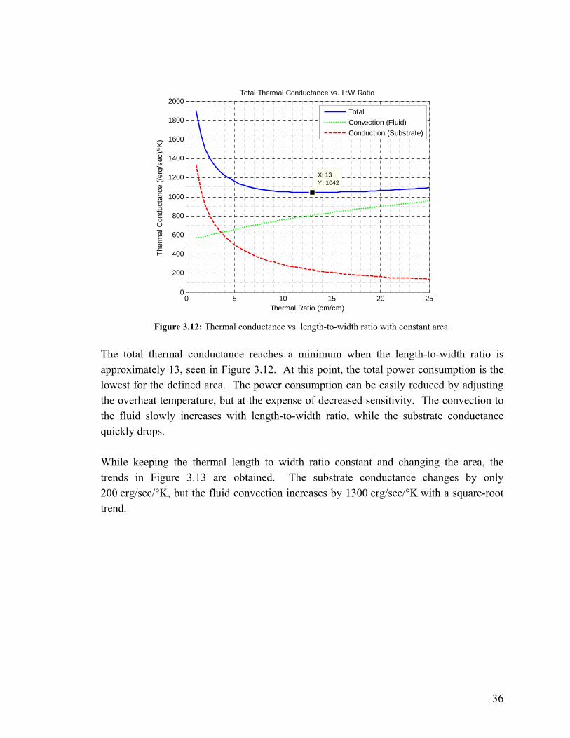
36
0 5 10 15 20 250
200
400
600
800
1000
1200
1400
1600
1800
2000
X: 13Y: 1042
Thermal Ratio (cm/cm)
Ther
mal
Con
duct
ance
((er
g/se
c)/ °K
)
Total Thermal Conductance vs. L:W Ratio
TotalConvection (Fluid)Conduction (Substrate)
Figure 3.12: Thermal conductance vs. length-to-width ratio with constant area.
The total thermal conductance reaches a minimum when the length-to-width ratio is approximately 13, seen in Figure 3.12. At this point, the total power consumption is the lowest for the defined area. The power consumption can be easily reduced by adjusting the overheat temperature, but at the expense of decreased sensitivity. The convection to the fluid slowly increases with length-to-width ratio, while the substrate conductance quickly drops. While keeping the thermal length to width ratio constant and changing the area, the trends in Figure 3.13 are obtained. The substrate conductance changes by only 200 erg/sec/°K, but the fluid convection increases by 1300 erg/sec/°K with a square-root trend.

37
From Figure 3.12 and Figure 3.13, it is shown that for maximum sensitivity, the heater should be designed for the largest area, and largest thermal length to width ratio. Making the heater length as long as possible will increase both the area and the thermal ratio. Increasing the heater width increases the area, but will decrease the thermal ratio. So, an optimum width where the convection conductance is at a maximum should exist. Figure 3.14 shows that the conductance to the fluid increases with the sensor width, but slowly starts to flatten. The conductance to the substrate linearly increases over the entire range, and starts to dominate the total conductance. Therefore, increasing the width will increase the sensitivity, but the amount of power lost to the substrate becomes problematic. When the heater width is smallest, the percent of the total conductance due to fluid convection is greatest, indicating that this geometry offers the most efficient tradeoff between power and sensitivity. Therefore, the ideal heater geometry should have the smallest value of WT, and will stretch across the entire channel width (i.e. LT = CW).
0 200 400 600 800 1000 1200 1400 16000
200
400
600
800
1000
1200
1400
1600
1800
2000
Heater Area (μm2)
Ther
mal
Con
duct
ance
((er
g/se
c)/ °K
)
Total Thermal Conductance vs. Heater Area
TotalConvection (Fluid)Conduction (Substrate)
Figure 3.13: Thermal conductance vs. heater area with length-to-width ratio held constant.
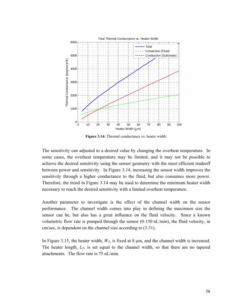
38
The sensitivity can adjusted to a desired value by changing the overheat temperature. In some cases, the overheat temperature may be limited, and it may not be possible to achieve the desired sensitivity using the sensor geometry with the most efficient tradeoff between power and sensitivity. In Figure 3.14, increasing the sensor width improves the sensitivity through a higher conductance to the fluid, but also consumes more power. Therefore, the trend in Figure 3.14 may be used to determine the minimum heater width necessary to reach the desired sensitivity with a limited overheat temperature. Another parameter to investigate is the effect of the channel width on the sensor performance. The channel width comes into play in defining the maximum size the sensor can be, but also has a great influence on the fluid velocity. Since a known volumetric flow rate is pumped through the sensor (0-150 nL/min), the fluid velocity, in cm/sec, is dependent on the channel size according to (3.31). In Figure 3.15, the heater width, WT, is fixed at 8 µm, and the channel width is increased. The heater length, LT, is set equal to the channel width, so that there are no tapered attachments. The flow rate is 75 nL/min.
0 10 20 30 40 50 60 70 80 90 1000
1000
2000
3000
4000
5000
6000
Heater Width (μm)
Ther
mal
Con
duct
ance
((er
g/se
c)/ °K
)
Total Thermal Conductance vs. Heater Width
TotalConvection (Fluid)Conduction (Substrate)
Figure 3.14: Thermal conductance vs. heater width.
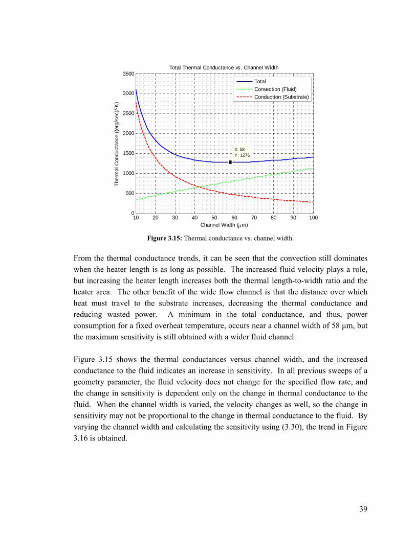
39
10 20 30 40 50 60 70 80 90 1000
500
1000
1500
2000
2500
3000
3500
X: 58Y: 1276
Channel Width (μm)
Ther
mal
Con
duct
ance
((er
g/se
c)/ °K
)
Total Thermal Conductance vs. Channel Width
TotalConvection (Fluid)Conduction (Substrate)
Figure 3.15: Thermal conductance vs. channel width.
From the thermal conductance trends, it can be seen that the convection still dominates when the heater length is as long as possible. The increased fluid velocity plays a role, but increasing the heater length increases both the thermal length-to-width ratio and the heater area. The other benefit of the wide flow channel is that the distance over which heat must travel to the substrate increases, decreasing the thermal conductance and reducing wasted power. A minimum in the total conductance, and thus, power consumption for a fixed overheat temperature, occurs near a channel width of 58 µm, but the maximum sensitivity is still obtained with a wider fluid channel. Figure 3.15 shows the thermal conductances versus channel width, and the increased conductance to the fluid indicates an increase in sensitivity. In all previous sweeps of a geometry parameter, the fluid velocity does not change for the specified flow rate, and the change in sensitivity is dependent only on the change in thermal conductance to the fluid. When the channel width is varied, the velocity changes as well, so the change in sensitivity may not be proportional to the change in thermal conductance to the fluid. By varying the channel width and calculating the sensitivity using (3.30), the trend in Figure 3.16 is obtained.

40
10 20 30 40 50 60 70 80 90 1000
0.5
1
1.5
2
2.5x 10
4
Channel Width (μm)
Sen
sitiv
ity (V
-sec
/cm
)
Figure 3.16: Sensitivity vs. channel width.
Figure 3.16 shows that the sensitivity not only increases with channel width seen in Figure 3.15, but increases exponentially. Therefore, according to basic thermal principles, it is drastically beneficial to make the channel wide. From the MATLAB analysis of the basic thermal properties and electrical characteristics of the sensor, it has been identified that the ideal shape for maximum conductance to the fluid and minimal power loss is a narrow sensor bridge stretching across the entire fluid channel. Since this model is based only on the fundamental physical laws, it may not be accurate in predicting the sensor behavior, but is helpful in design and preliminary analysis. The main parameter that is overlooked in the mathematical model and MATLAB analysis is the dependence of the thermal conductance on the orientation of the sensor. The expression for spreading resistance comes with the stipulation that the thermal length-to-width ratio be 1 or greater, even though the function is even when plotted versus the logarithm of the length to width ratio. Therefore, if the sensor is ten times wider than it is long, the thermal spreading resistance, and dependence on fluid velocity, will be the same as a sensor with length that is ten times the width. At zero fluid velocity, this is not an issue, but when the orientation relative to the fluid flow is different, the result will not be the same. No simple mathematical solution exists to describe this, and with the
41
complexity of the spreading resistance equation combined with the fluid velocity profile around the sensor, an empirical analysis would be simpler and more accurate. The other major fault in this prediction for thermal behavior arises from the value of L, the characteristic length, used to calculate the Reynolds number and Nusselt number. A characteristic length value is used in several dimensionless numbers in fluid dynamics, including the Reynolds number, Knudsen number, Péclet number, and many others. These dimensionless numbers are primarily used to determine what effects are dominant and what sets of equations apply most accurately in a particular scenario. For example, a low Reynolds number is indicative of fluid flow in the laminar regime, while a high Reynolds number indicates that the flow is turbulent. The exact cut-off for the Reynolds number between laminar and turbulent flow depends on the system. The exact value of the dimensionless number is usually not critical, and a recommendation is often given for the value of the characteristic length for certain scenarios. In a cylindrical pipe, the characteristic length used in the Reynolds number is the diameter of the pipe. Once the pipe becomes elliptical or square, or a flow sensor is added, the Reynolds number changes. In this representation, the exact value of the Nusselt number is important. So, a considerable difference in the Nusselt number may be calculated whether the channel width, heater length, or some other value is used for characteristic length. Here, the channel width is used for the value of the characteristic length. The analysis of relative effects from different design parameters is still valid and useful. Using the mathematical formulas and MATLAB analysis presented, the sensor shape to obtain the most efficient tradeoff between power and sensitivity has been determined, which can be used to guide the design of fabricated sensors. If the desired sensitivity cannot be obtained with the most efficient sensor shape, the relative improvements in sensitivity obtained by changing different parameters, such as the heater width, at the cost of more power consumption, are shown. To refine the mathematical expressions describing the heat transfer, a multiphysics finite-element analysis can be used. This will be able to take into the account the orientation of the sensor relative to the fluid flow, and an accurate form of King’s Law, in (3.22), applicable to this particular sensor design can be determined. The finite-element analysis depends only on fluid properties and geometry explicitly defined by a CAD model.

42
Therefore, there will be no error due to poorly defined variables like the characteristic length. REFERENCES
[1] Bejan, A. and A. Kraus, Heat Transfer Handbook. 2003: John Wiley & Sons. [2] Damean, N., P.P.L. Regtien, and M. Elwenspoek, “Heat transfer in a MEMS for
microfluidics,” Sensors and Actuators A: Physical, 2003. 105(2): p. 137-149. [3] Qu, W., G.M. Mala, and D. Li, “Heat transfer for water flow in trapezoidal silicon
microchannels,” International Journal of Heat and Mass Transfer, 2000. 43(21): p. 3925-3936.
[4] Yovanovich, M.M., Y.S. Muzychka, and J.R. Culham, “Spreading Resistance of Isoflux Rectangles and Strips on Compound Flux Channels,” Journal of Thermodynamics and Heat Transfer, 1999. 13(4).

43
FINITE-ELEMENT ANALYSIS In addition to the numerical analysis using MATLAB, finite-element analysis simulations are performed. ANSYS Multiphysics software is used, which can simulate structural mechanics, heat transfer, fluid flow, acoustics, electromagnetics, and the energy coupling between each of the domains (e.g. the production of heat due to electrical current). First, ANSYS will be used to characterize the thermal spreading resistance from a rectangular body to an infinite fluid as a function of fluid velocity. In the mathematical model in Chapter 3, this is done using the thermal spreading resistance at zero flow rate, multiplied by the Nusselt number for a flat surface. This method neglects the orientation of the sensor relative to the fluid flow. Because the sensor is not truly a flat plate, the actual behavior may differ from that predicted by the expression used for the Nusselt number. Next, ANSYS will be used to model the entire system, with the fluid channel, sensor, and substrate. Most of all, this will reveal the deviation in thermal spreading conductance when the fluid body is no longer infinite, but is constrained to a fluid channel. In finite-element analysis, a body (e.g. a solid object or a collection of fluid) is broken up into many (on the order of millions) smaller pieces (elements). By algebraically calculating the forces and fluxes acting on each element from its contiguous elements (e.g. mechanical force, temperature differential, electrical potential, etc), and iterating the process until a convergence is reached, the effects of complicated partial differential equations, geometries, and material boundaries are greatly simplified. While the result is ultimately an approximation, with extremely small elements and several iterations, the results can be extremely accurate and consistent.
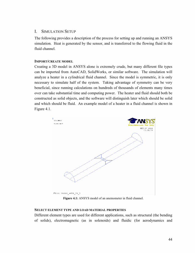
44
I. SIMULATION SETUP The following provides a description of the process for setting up and running an ANSYS simulation. Heat is generated by the sensor, and is transferred to the flowing fluid in the fluid channel.
IMPORT/CREATE MODEL Creating a 3D model in ANSYS alone is extremely crude, but many different file types can be imported from AutoCAD, SolidWorks, or similar software. The simulation will analyze a heater in a cylindrical fluid channel. Since the model is symmetric, it is only necessary to simulate half of the system. Taking advantage of symmetry can be very beneficial, since running calculations on hundreds of thousands of elements many times over can take substantial time and computing power. The heater and fluid should both be constructed as solid objects, and the software will distinguish later which should be solid and which should be fluid. An example model of a heater in a fluid channel is shown in Figure 4.1.
Figure 4.1: ANSYS model of an anemometer in fluid channel.
SELECT ELEMENT TYPE AND LOAD MATERIAL PROPERTIES Different element types are used for different applications, such as structural (the bending of solids), electromagnetic (as in solenoids) and fluidic (for aerodynamics and

45
convection) analyses. In this simulation, the element type FLUID142 is chosen which will account for heat transfer and fluid dynamics. Material properties can be loaded that include the thermal conductivity, density, specific heat, and viscosity (for the fluid only). Different materials and element types can be assigned to different volumes in the model.
MESH THE MODEL The model is divided into thousands of small elements by meshing. The shapes of these elements are determined by the element type. In these simulations, the shapes will be tetrahedral. This step can be quite important, as elements that are too coarse can fail to accurately represent the model, and the simulation may fail to converge. Elements that are too small can take up too many computing resources to run the simulation. Meshing of the anemometer model is also difficult because the thin-film heater, a structure with relatively small features, must interact with the much larger fluid channel. With the Smart Sizing feature, the elements of the fluid near the heater can be small, and the size of the elements will increase as the distance from the heater increases. This is often convenient, but problems with convergence are often encountered. Alternatively, if computer resources are available, small element sizes can be used in the entire model. Figure 4.2 shows a meshed anemometer and fluid channel model with a constant element size.
Figure 4.2: Meshed ANSYS model.

46
APPLY BOUNDARY CONDITIONS AND LOADS This step defines the forces at work within the system. For fluidic constraints, the fluid pressure and fluid velocity may be defined. In 3D analyses, both of these are defined on areas. Fluid properties are also entered, which when combined with the fluid geometry, determine the relationship between pressure and velocity. To model fluid in a channel or pipe, a constraint of zero fluid velocity is applied to the edge of the fluid body, enforcing the no-slip condition. For thermal constraints, temperature, heat flux, heat generation, and film coefficient can be defined. A temperature constraint will hold a surface at constant temperature, allowing it to act as a heat source or sink if other constraints demand so. Heat flux can be used to define the heat produced or transferred from a surface, and heat generation can be used to define heat produced by a volume, as in Joule heating of a resistor. Constraining the film coefficient of an area is helpful in modeling heat transfer to another body of known temperature, if the parameter h, as described in Chapter 3 is known. In Figure 4.3, the yellow markers represent fluid pressure constraints at the outlet, red markers represent fluid velocity constraints at the inlet and channel walls, and orange markers represent temperature constraints.
Figure 4.3: ANSYS model with loads applied.
47
RUN SIMULATION After the material properties, loads, and constraints are entered into the program, the simulation runs with several (between 10 and 100) iterations to find the fluid velocity, pressure, and temperature on elements unconstrained. Since the heat generated is fixed, the temperature which the sensor rises to is observed at different flow rates. From the heat generated divided by the overheat temperature, the thermal conductivity to the substrate and the fluid is calculated.
II. THERMAL SPREADING CONDUCTANCE VERSUS VELOCITY The first set of simulations performed is designed to determine the effect of sensor geometry, which includes the area and length-to-width ratio, on the thermal conductance to the fluid. The greatest benefit of multiphysics simulation software is that the behavior of systems with complex geometries can be predicted. When there is symmetry between an object and the phenomenon being analyzed, the behavior can typically be predicted very accurately with simple mathematical analysis. For example, the radially emanating electric field from a charged sphere can be analyzed easily using calculus. However, the radially emanating electric field from a charged cube is much more difficult to represent mathematically. This is also the case in the equation for the thermal spreading resistance, Rconvec0, from a rectangle, (4.1), initially presented in Chapter 3.
( )⎥⎥⎥
⎦
⎤
⎢⎢⎢
⎣
⎡
⎟⎟⎟
⎠
⎞
⎜⎜⎜
⎝
⎛
⎟⎟⎠
⎞⎜⎜⎝
⎛+−+++⎟⎟
⎠
⎞⎜⎜⎝
⎛= −−
23
2311
01111
3sinh11sinh
ζζζζ
ζζπ
ζ
Tfluidconvec
AkR
(4.1) In (4.1), kfluid is the thermal conductivity of the fluid, ζ is the length-to-width ratio, and AT is the sensor area. The complexity of the equation for thermal resistance, combined with the non-linearities of fluid flow, make simulation and trend-fitting the most effective method for determining the effect of sensor geometry on thermal conductance to non-stagnant fluid. The King’s Law parameters described in Chapter 3 will now become functions of sensor area and thermal ratio, as in (4.2), where Gconvec is the thermal spreading conductance, u the fluid velocity, and β and χ are fitting parameters. ( ) ( )( )TTA
TTconvecconvec uAGG ζχζβ ,0 ,1+= (4.2)

48
The simulation consists simply of two joined rectangular prisms, as shown in Figure 4.4. One prism is much larger than the other; the larger modeling an infinite half-space of water, and the smaller, a heat source. The area at which the two rectangular prisms are joined represents the sensor interface with the fluid. The area of the interface is varied between 25 square micrometers and 2025 square micrometers. The length-to-width ratio is varied between 0.04 and 25. Figure 4.5 shows the meshed simulation model, which makes use of the Smart Sizing feature. On the smaller rectangular prism and at the interface with the larger prism, the mesh size is comparable to the critical dimension of the smaller rectangular prism. As the mesh expands to the edges of the larger rectangular prism, the size of the elements grows.
Figure 4.4: Large and small rectangular prisms representing infinite half-space of fluid and heating
element.

49
Figure 4.5: Meshed rectangular prisms using finest smart sizing resolution.
The fluid block is given the thermal and fluidic properties of water, and the heating block is assigned “ideal” conditions. Ideal conditions include a very small heat capacity, very small density, and very large thermal conductivity compared to water. This will force all of the elements of the heating block to have the same temperature. An initial condition of 310°K is applied to the elements of the fluid, and the side opposite the heater is fixed at 310°K. The heater generates 10,000 ergs per second (1 milliwatt), which is entirely transferred to the fluid through the shared area. As the heat is generated and dissipated to the fluid, the heater temperature will increase, and reach a steady state. This temperature divided by 10,000 ergs per second is the thermal resistance. The velocity of the fluid is varied from 0 to 0.3 centimeters per second, and the change in thermal resistance observed. Figure 4.6 shows a temperature plot of the simulation results when the fluid is not moving. The highest temperature points are located closest to the sensor area, and the fluid temperature shows an inverse relationship with distance to the sensor. When the distance from the sensor is much greater than the sensor dimensions, the contour along which the temperature does not change is much like a sphere, revealing the radial symmetry of diffusion of heat.

50
The lowest temperature contour extends beyond the boundaries of the “infinite” fluid. However, the simulation convergence criteria are met and the simulation terminates before the contour extends farther. The defined simulation convergence requires that the temperature not change more than one part per trillion (one ten-billionth of a percent) between consecutive iterations. The example in Figure 4.6 is also the sensor with the largest area and length-to-width ratio tested, and sensors with smaller areas to do not show contours outside of the fluid. A fluid velocity constraint is applied to the bottom and top walls of the larger rectangular prism, for inlet and outlet, respectively. A vector plot of the fluid velocity is shown in Figure 4.7, with units of cm/sec. Around the sensor surface, the fluid encounters friction and moves much less freely. Therefore, near the sensor, the fluid velocity is low. This gradient in fluid velocity near the sensor is the source of the immense complexity associated with mathematically deriving an expression for the thermal conductance versus flow rate.
Figure 4.6: Contour plot of temperature with fluid velocity fixed at zero.
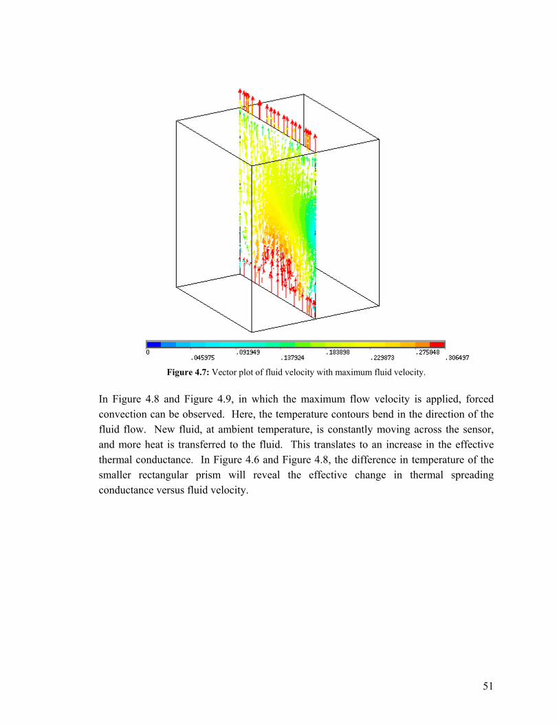
51
Figure 4.7: Vector plot of fluid velocity with maximum fluid velocity.
In Figure 4.8 and Figure 4.9, in which the maximum flow velocity is applied, forced convection can be observed. Here, the temperature contours bend in the direction of the fluid flow. New fluid, at ambient temperature, is constantly moving across the sensor, and more heat is transferred to the fluid. This translates to an increase in the effective thermal conductance. In Figure 4.6 and Figure 4.8, the difference in temperature of the smaller rectangular prism will reveal the effective change in thermal spreading conductance versus fluid velocity.
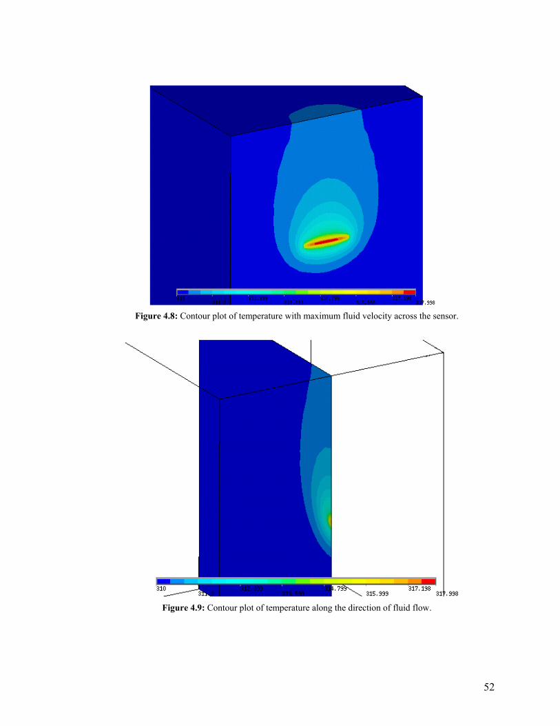
52
Figure 4.8: Contour plot of temperature with maximum fluid velocity across the sensor.
Figure 4.9: Contour plot of temperature along the direction of fluid flow.

53
Between the two simulations in Figure 4.6 and Figure 4.8, the maximum temperature drops by just over 1.5 °K. Since an overheat temperature of only 9.5°K is observed with zero fluid flow, this represents a drop of 16%. The associated change in thermal conductance is approximately 250 ergs/sec/°K. This set of simulations to determine the effect of sensor area and length to width ratio on thermal conductance versus fluid velocity is performed with 9 values of sensor area, 11 values of length-to-width ratio, and 6 fluid velocities, resulting in 594 simulations. The area is varied between 25 µm2 and 2025 µm2, and the length-to-width ratio is varied between 1/25 and 25. The fluid velocity is chosen to be between 0 and 0.3 cm/sec, which is approximately the maximum fluid velocity in a 32 µm wide fluid channel for a flow rate of 150 nL/min. The process of configuring and running this massive set of simulations is facilitated using MATLAB. A MATLAB script is written that will go through the different area, ratio, and flow rate values, and create an input file read by ANSYS. When one simulation is completed, the temperature data of the heating element is written to a text file, and ANSYS will continue on to the next simulation. Only the temperature of the heating element must be recorded, since this represents the overheat temperature of the sensor. The heat generation divided by the overheat temperature is used to calculate the thermal conductance. Another MATLAB script is written to read all of the text files produced by ANSYS, and to analyze the results. All of the MATLAB scripts written to aid in the ANSYS simulation and data analysis can be found in Appendix B. The MATLAB scripts responsible for data analysis produce a 3D surface plot of thermal conductance versus area and length-to-width ratio. For each flow rate analyzed, a different plot is obtained. At zero flow rate, in Figure 4.10, the a plane of symmetry is seen where the log of the length-to-width ratio equals zero. When the maximum flow velocity of 0.3 cm/sec is applied, as in Figure 4.11, the plot becomes asymmetric. As expected, the thermal conductance of the wide sensor, with low length-to-width ratio, is less than that of the long sensor, since the wide sensor redundantly heats a smaller cross-section of fluid passing over it. The long sensor exchanges heat with a larger cross-section of fluid, for a shorter amount of time.

54
0500
10001500
20002500
-4-2
0
240
200
400
600
800
1000
1200
Area (μm2)Log(Ratio (cm/cm))
Ther
mal
Con
duct
ance
(erg
/sec
/ °K)
-4 -3 -2 -1 0 1 2 3 40
200
400
600
800
1000
1200
Log(Ratio (cm/cm))
Ther
mal
Con
duct
ance
(erg
/sec
/ °K)
Figure 4.10: Surface plot of thermal conductance versus length-to-width ratio and area at zero flow rate.

55
0500
10001500
20002500
-4-2
0
240
500
1000
1500
Area (μm2)Log(Ratio (cm/cm))
Ther
mal
Con
duct
ance
(erg
/sec
/ °K)
-4 -3 -2 -1 0 1 2 3 40
200
400
600
800
1000
1200
1400
1600 X: 2025Y: 3.219Z: 1388
Log(Ratio (cm/cm))
X: 2025Y: -3.219Z: 1376
Ther
mal
Con
duct
ance
(erg
/sec
/ °K)
Figure 4.11: Surface plot of thermal conductance versus length-to-width ratio and area at 0.3 cm/sec.
The difference in thermal conductance between positive and negative values of the logarithm of length-to-width ratio is small compared to the entire range of thermal conductance. If just the difference in thermal conductance at maximum flow rate and zero flow rate is plotted, the asymmetry of the thermal conductance versus the length-to-width ratio is more noticeable. The plot in Figure 4.12 shows the difference in thermal conductance at the maximum flow rate and at zero flow rate (i.e. Gconvec_max – Gconvec0).
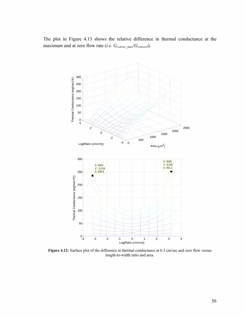
56
The plot in Figure 4.13 shows the relative difference in thermal conductance at the maximum and at zero flow rate (i.e. Gconvec_max/Gconvec0).
0500
10001500
20002500
-4-2
0
240
50
100
150
200
250
300
Area (μm2)Log(Ratio (cm/cm))
Ther
mal
Con
duct
ance
(erg
/sec
/ °K)
-4 -3 -2 -1 0 1 2 3 40
50
100
150
200
250
300X: 2025Y: 3.219Z: 251.1
Log(Ratio (cm/cm))
X: 2025Y: -3.219Z: 235.9
Ther
mal
Con
duct
ance
(erg
/sec
/ °K)
Figure 4.12: Surface plot of the difference in thermal conductance at 0.3 cm/sec and zero flow versus
length-to-width ratio and area.

57
0500
10001500
20002500
-4-2
0
241
1.05
1.1
1.15
1.2
1.25
Area (μm2)Log(Ratio (cm/cm))
-4 -3 -2 -1 0 1 2 3 41
1.05
1.1
1.15
1.2
1.25 X: 2025Y: 3.219Z: 1.221
Log(Ratio (cm/cm))
X: 2025Y: -3.219Z: 1.207
Figure 4.13: Surface plot of the ratio of thermal conductance at 0.3 cm/sec to zero flow versus length-to-
width ratio and area. As described in Chapter 3, the spreading resistance dependence on the logarithm of the length-to-width ratio is fit to a quartic function. The thermal spreading resistance expression in (4.1) is modified to the quartic thermal spreading resistance function in (4.3).

58
( )012
23
34
401 ccccc
AkRconvec +Ζ+Ζ+Ζ+Ζ=
π (4.3)
The variable Z is the natural logarithm of the length-to-width ratio (i.e.: Z=ln(ζ)). The coefficients of the terms of the polynomial, c0-c4, are fitted to match the simulation data. Since the data obtained from the simulations is represented as thermal conductance, and not resistance, the inverse of (4.3) is used, given in (4.4).
( )012
23
34
40 ccccc
AkGconvec +Ζ+Ζ+Ζ+Ζ=
π (4.4)
For each flow rate, the values of c4-c0 are shown in Table 4.1. The values given in the table are valid for the area, A, in units of cm2. If c4-c0 are each made to be functions of fluid velocity, then the denominator of (4.4) is a function of fluid velocity, and (4.4) becomes (4.5), which is valid for Gconvec at all fluid velocities, and not just Gconvec0.
( ) ( ) ( ) ( ) ( )( )ucucucucucAkGconvec
012
23
34
4 +Ζ⋅+Ζ⋅+Ζ⋅+Ζ⋅=
π (4.5)
The R2 values of the fit to the thermal conductance data using (4.5) are listed in Table 4.1, with the associated c values, and is never below 99.5%, indicating a good fit. The coefficients c4 and c3 are invariant over the range of flow rates analyzed. The linear coefficient, c1, changes significantly since the trend becomes asymmetric over Z equal to zero. The c2 and c0 terms also change versus flow rate. Table 4.1: Values of the Coefficients of the Quartic Function fitted to Simulation Data of
Thermal Spreading Conductance. Velocity (cm/sec) c4 c3 c2 c1 c0 R2
0.00 0.0017 -0.0002 -0.0554 0.001 1.1107 0.9953 0.06 0.0017 -0.0002 -0.0552 0.0009 1.0887 0.9960 0.12 0.0017 -0.0002 -0.055 0.0009 1.0537 0.9966 0.18 0.0017 -0.0002 -0.0548 0.0008 1.0287 0.9966 0.24 0.0017 -0.0002 -0.0547 0.0007 1.0115 0.9965 0.30 0.0017 -0.0002 -0.0545 0.0005 0.9978 0.9963

59
The thermal conductance versus area and length-to-width ratio is calculated using the fitted parameters. The difference in thermal conductance between the maximum flow rate and zero flow rate is shown in Figure 4.14.
Figure 4.14: Surface plot of the difference in thermal conductance at flow rate of 0.3 cm/sec and zero flow
rate, calculated from fitted quartic function for thermal spreading conductance.
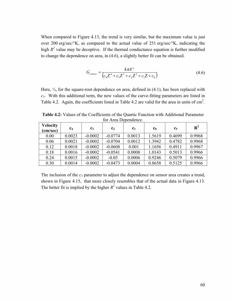
60
When compared to Figure 4.13, the trend is very similar, but the maximum value is just over 200 erg/sec/°K, as compared to the actual value of 251 erg/sec/°K, indicating the high R2 value may be deceptive. If the thermal conductance equation is further modified to change the dependence on area, in (4.6), a slightly better fit can be obtained.
( )012
23
34
4
5
cccccAkG
c
convec +Ζ+Ζ+Ζ+Ζ=
π(4.6)
Here, ½, for the square-root dependence on area, defined in (4.1), has been replaced with c5. With this additional term, the new values of the curve-fitting parameters are listed in Table 4.2. Again, the coefficients listed in Table 4.2 are valid for the area in units of cm2. Table 4.2: Values of the Coefficients of the Quartic Function with Additional Parameter
for Area Dependence. Velocity (cm/sec) c4 c3 c2 c1 c0 c5 R2
0.00 0.0023 -0.0002 -0.0774 0.0013 1.5619 0.4699 0.9968 0.06 0.0021 -0.0002 -0.0704 0.0012 1.3942 0.4782 0.9968 0.12 0.0018 -0.0002 -0.0608 0.001 1.1656 0.4911 0.9967 0.18 0.0016 -0.0002 -0.0541 0.0008 1.0143 0.5013 0.9966 0.24 0.0015 -0.0002 -0.05 0.0006 0.9246 0.5079 0.9966 0.30 0.0014 -0.0002 -0.0473 0.0004 0.8658 0.5125 0.9966
The inclusion of the c5 parameter to adjust the dependence on sensor area creates a trend, shown in Figure 4.15, that more closely resembles that of the actual data in Figure 4.13. The better fit is implied by the higher R2 values in Table 4.2.

61
0500
10001500
20002500
-4-2
0
24
-50
0
50
100
150
200
250
Area (μm2)Log(Ratio (cm/cm))
Ther
mal
Con
duct
ance
(erg
/sec
/ °K)
-4 -3 -2 -1 0 1 2 3 4-50
0
50
100
150
200
250
Log(Ratio (cm/cm))
Ther
mal
Con
duct
ance
(erg
/sec
/ °K)
Figure 4.15: Surface plot of the difference in thermal conductance at flow rates of 0.3 cm/sec and 0, calculated from the fitted quartic function with area dependence for thermal spreading conductance.
The curve-fitting parameters that vary over the range of flow velocities, are plotted. If the best-fit linear trend is determined, mathematical expressions for the coefficients can be determined with R2 values between 95% and 99%, as in Figure 4.16.

62
C0
y = -2.4003x + 1.5144R2 = 0.9567
0
0.2
0.4
0.6
0.8
1
1.2
1.4
1.6
1.8
0 0.05 0.1 0.15 0.2 0.25 0.3
Flow Velocity (cm/sec)
C1
y = -0.0031x + 0.0013R2 = 0.9922
0
0.0002
0.0004
0.0006
0.0008
0.001
0.0012
0.0014
0.0016
0 0.05 0.1 0.15 0.2 0.25 0.3
Flow Velocity (cm/sec)
C2y = 0.104x - 0.0756
R2 = 0.9629
-0.09
-0.08
-0.07
-0.06
-0.05
-0.04
-0.03
-0.02
-0.01
0
0 0.05 0.1 0.15 0.2 0.25 0.3
Flow Velocity (cm/sec)
C4y = -0.0031x + 0.0022
R2 = 0.9606
0
0.0005
0.001
0.0015
0.002
0.0025
0 0.05 0.1 0.15 0.2 0.25 0.3
Flow Velocity (cm/sec)
C5
y = 0.1487x + 0.4712R2 = 0.9771
0.46
0.47
0.48
0.49
0.5
0.51
0.52
0 0.05 0.1 0.15 0.2 0.25 0.3
Flow Velocity (cm/sec)
Figure 4.16: Plot of curve fitting coefficients, C0, C1, C2, C4, and C5 versus flow velocity with linear
trendlines. Linear Fittings for Thermal Conductance Equation:
0022.00031.04 +−= ucL
000203 .cL −=
0756.0104.02 −= ucL
0013.00031.01 +−= ucL 5144.14003.20 +−= ucL
4712.01487.05 += ucL
If a second order polynomial fit is used, trendlines with fits better than 99% for each coefficient are obtained, shown in Figure 4.17.

63
C0
y = 5.4568x2 - 4.0373x + 1.5799R2 = 0.9946
0
0.2
0.4
0.6
0.8
1
1.2
1.4
1.6
1.8
0 0.05 0.1 0.15 0.2 0.25 0.3
Flow Velocity (cm/sec)
C1
y = -0.0025x2 - 0.0024x + 0.0013R2 = 0.9971
0
0.0002
0.0004
0.0006
0.0008
0.001
0.0012
0.0014
0 0.05 0.1 0.15 0.2 0.25 0.3
Flow Velocity (cm/sec)
C2y = -0.2158x2 + 0.1687x - 0.0782
R2 = 0.9947
-0.09
-0.08
-0.07
-0.06
-0.05
-0.04
-0.03
-0.02
-0.01
0
0 0.05 0.1 0.15 0.2 0.25 0.3
Flow Velocity (cm/sec)
C4
y = 0.0064x2 - 0.005x + 0.0023R2 = 0.9926
0
0.0005
0.001
0.0015
0.002
0.0025
0 0.05 0.1 0.15 0.2 0.25 0.3
Flow Velocity (cm/sec)
C5
y = -0.2168x2 + 0.2137x + 0.4686R2 = 0.993
0.465
0.47
0.475
0.48
0.485
0.49
0.495
0.5
0.505
0.51
0.515
0.52
0 0.05 0.1 0.15 0.2 0.25 0.3
Flow Velocity (cm/sec)
Figure 4.17: Plot of curve fitting coefficients, C0, C1, C2, C4, and C5 versus flow velocity with second-
order polynomial trendlines. Second-order Polynomial Fittings for Thermal Conductance Equation:
0023.0005.00064.0 24 +−= uucP
000203 .cP −=
0782.01687.02158.0 22 −+−= uucP
0013.00024.00025.0 21 +−−= uucP
58.1037.4457.5 20 +−= uucP
4686.02137.02168.0 25 ++−= uucP

64
With c5-c0 defined as functions of fluid velocity, these can be combined in (4.6) to create an equation for the thermal spreading conductance as a function of sensor area, length-to-width ratio, and fluid velocity. In the initial analysis, disjoint functions for geometry and fluid velocity were multiplied together, which produced an incomplete formulation for the thermal spreading conductance from the sensor. Alternatively, instead of approximating (4.1) and incorporating the fluid velocity, the King’s Law parameters can be calculated for each sensor geometry. King’s Law states that: χbuah += or ( )χβuGG convecconvec += 10 . (4.7) The term Gconvec0 is the thermal conductance at zero fluid velocity, calculated by the inverse of (4.1), and the thermal conductance will increase with fluid velocity according to the fitting parameters β and χ. Gconvec0 is obtained from the simulation results at zero flow velocity. To obtain β and χ, the thermal conductance values obtained from simulations of the same sensor geometry with different fluid velocities are normalized by dividing by Gconvec0. A least-square error fit is used to find β and χ that match the trend. A plot of the values of β are shown in Figure 4.18, and a plot of the values of χ are shown in Figure 4.19.
0500
10001500
20002500
-4-2
0
240
0.2
0.4
0.6
0.8
Area (μm2)Log(Ratio (cm/cm)) -4 -3 -2 -1 0 1 2 3 4
0
0.1
0.2
0.3
0.4
0.5
0.6
0.7
Log(Ratio (cm/cm)) Figure 4.18: King’s Law coefficient, β, versus sensor area and length-to-width ratio fitted to the simulation
data for thermal conductance.
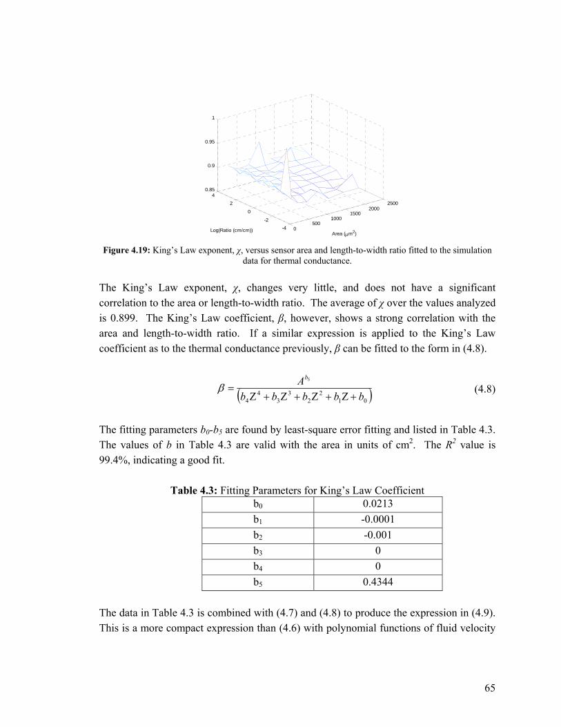
65
0500
10001500
20002500
-4-2
0
24
0.85
0.9
0.95
1
Area (μm2)Log(Ratio (cm/cm))
Figure 4.19: King’s Law exponent, χ, versus sensor area and length-to-width ratio fitted to the simulation
data for thermal conductance. The King’s Law exponent, χ, changes very little, and does not have a significant correlation to the area or length-to-width ratio. The average of χ over the values analyzed is 0.899. The King’s Law coefficient, β, however, shows a strong correlation with the area and length-to-width ratio. If a similar expression is applied to the King’s Law coefficient as to the thermal conductance previously, β can be fitted to the form in (4.8).
( )012
23
34
4
5
bbbbbAb
+Ζ+Ζ+Ζ+Ζ=β (4.8)
The fitting parameters b0-b5 are found by least-square error fitting and listed in Table 4.3. The values of b in Table 4.3 are valid with the area in units of cm2. The R2 value is 99.4%, indicating a good fit.
Table 4.3: Fitting Parameters for King’s Law Coefficient b0 0.0213 b1 -0.0001 b2 -0.001 b3 0 b4 0 b5 0.4344
The data in Table 4.3 is combined with (4.7) and (4.8) to produce the expression in (4.9). This is a more compact expression than (4.6) with polynomial functions of fluid velocity

66
for c0-c5 values. King’s Law is commonly used, but fitted to experimental data that produce different values of β and χ for individual sensors. The expanded version of King’s Law in (4.9) is valuable, since it will predict a form of King’s Law for various sensor shapes.
( )( ) ⎟⎟⎠
⎞⎜⎜⎝
⎛+Ζ⋅−+Ζ⋅−
+= 899.02
4344.0
0 0213.00001.0001.01 uAGG convecconvec (4.9)
With more accurate mathematical expressions for the thermal spreading conductance versus fluid velocity and sensor geometry, the optimum sensor design can be investigated. In order to accurately compare the performance of different sensor geometries, the sensitivity must be determined. With the two equations developed describing the thermal conductance versus flow velocity and sensor geometry, the change in thermal conductance versus flow rate can be determined. Taking the derivative of the thermal conductance versus flow velocity yields a sensitivity in terms of erg/sec/°K/(cm/sec). For the expression based on (4.6), the sensitivity expression in (4.10) is calculated.
( )012
23
34
4
5
cccccAkG
c
convec +Ζ+Ζ+Ζ+Ζ=
π
( ) ( )( )201
22
33
44
0122334401
22
33
44
5 55 ln
cccccdudc
dudcZ
dudcZ
dudcZ
dudcZAkccccc
dudcAAk
dudG
cc
convec
+Ζ+Ζ+Ζ+Ζ
⎟⎠⎞
⎜⎝⎛ ++++⋅−+Ζ+Ζ+Ζ+Ζ⋅⋅⋅
=ππ
.
(4.10) For the expression based on King’s Law in (4.7) and (4.8), the sensitivity is calculated in (4.11).
( )χβuGG convecconvec += 10
100
−+= χχ βχβ uGduduG
dudG
convecconvecconvec
( ) ( )( )201
22
33
44
022334401
22
33
44
5 55 ln
bbbbbdudb
dudb
dudb
dudb
dudbAbbbbb
dudb
AA
dud
bb
+Ζ+Ζ+Ζ+Ζ
⎟⎠⎞
⎜⎝⎛ +Ζ+Ζ+Ζ+Ζ⋅−+Ζ+Ζ+Ζ+Ζ⋅⋅⋅
=β

67
Since b0 – b5 are independent of fluid velocity,
0=dudβ ,
and
10
−= χβχuGdu
dGconvec
convec . (4.11)
The change in thermal conductance represents the sensitivity due to the thermal properties of the sensor. To determine whether one sensor is more sensitive than another, it is the relative sensitivity that is important.
du
dGS convec=econductanc (4.12)
0
relativeconvec
convec
Gdu
dG
S = (4.13)
[ ] cmsec
Ksecerg
seccmK
secerg
relative =°
°
=S (4.14)
Using (4.6) with polynomial fitting equations cP0-cP5, and a fluid velocity value of 0.15 cm/sec, the plot in Figure 4.20 is obtained. At very low values for the area, the sensitivity is computed to be negative. This is most likely not what truly happens, but instead, is an artifact of the trend fitting.
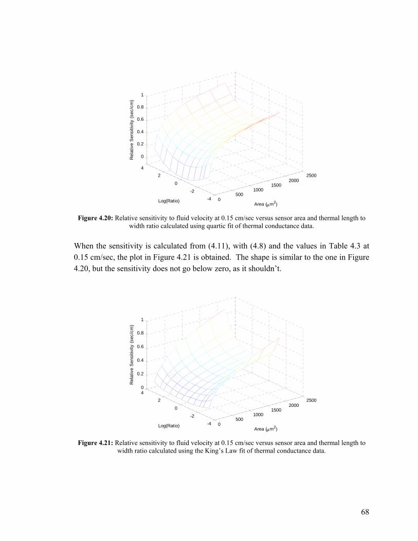
68
0500
10001500
20002500
-4-2
0
24
0
0.2
0.4
0.6
0.8
1
Area (μm2)Log(Ratio)
Rel
ativ
e S
ensi
tivity
(sec
/cm
)
Figure 4.20: Relative sensitivity to fluid velocity at 0.15 cm/sec versus sensor area and thermal length to
width ratio calculated using quartic fit of thermal conductance data. When the sensitivity is calculated from (4.11), with (4.8) and the values in Table 4.3 at 0.15 cm/sec, the plot in Figure 4.21 is obtained. The shape is similar to the one in Figure 4.20, but the sensitivity does not go below zero, as it shouldn’t.
0500
10001500
20002500
-4-2
0
240
0.2
0.4
0.6
0.8
1
Area (μm2)Log(Ratio)
Rel
ativ
e S
ensi
tivity
(sec
/cm
)
Figure 4.21: Relative sensitivity to fluid velocity at 0.15 cm/sec versus sensor area and thermal length to
width ratio calculated using the King’s Law fit of thermal conductance data.
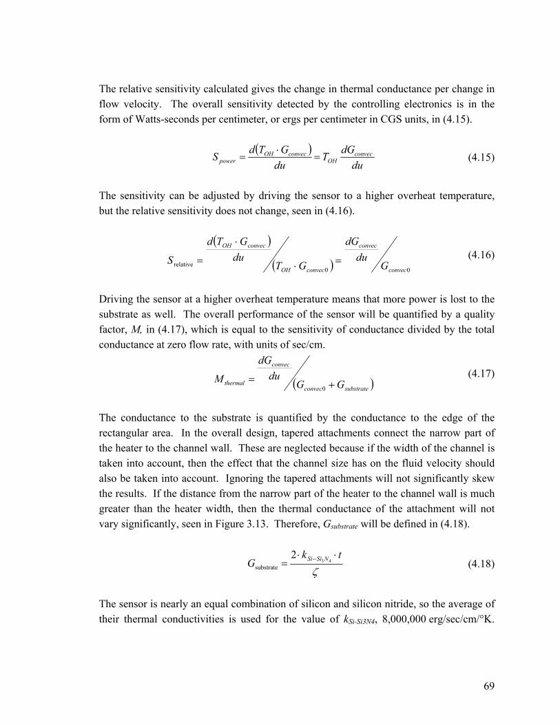
69
The relative sensitivity calculated gives the change in thermal conductance per change in flow velocity. The overall sensitivity detected by the controlling electronics is in the form of Watts-seconds per centimeter, or ergs per centimeter in CGS units, in (4.15).
( )
dudGT
duGTdS convec
OHconvecOH
power =⋅
= (4.15)
The sensitivity can be adjusted by driving the sensor to a higher overheat temperature, but the relative sensitivity does not change, seen in (4.16).
( )
( ) 00relative
convec
convec
convecOH
convecOH
Gdu
dG
GTdu
GTd
S =⋅
⋅
= (4.16)
Driving the sensor at a higher overheat temperature means that more power is lost to the substrate as well. The overall performance of the sensor will be quantified by a quality factor, M, in (4.17), which is equal to the sensitivity of conductance divided by the total conductance at zero flow rate, with units of sec/cm.
( )substrateconvec
convec
thermal GGdu
dG
M +=0
(4.17)
The conductance to the substrate is quantified by the conductance to the edge of the rectangular area. In the overall design, tapered attachments connect the narrow part of the heater to the channel wall. These are neglected because if the width of the channel is taken into account, then the effect that the channel size has on the fluid velocity should also be taken into account. Ignoring the tapered attachments will not significantly skew the results. If the distance from the narrow part of the heater to the channel wall is much greater than the heater width, then the thermal conductance of the attachment will not vary significantly, seen in Figure 3.13. Therefore, Gsubstrate will be defined in (4.18).
ζ
tkG NSiSi ⋅⋅
= − 432
substrate (4.18)
The sensor is nearly an equal combination of silicon and silicon nitride, so the average of their thermal conductivities is used for the value of kSi-Si3N4, 8,000,000 erg/sec/cm/°K.
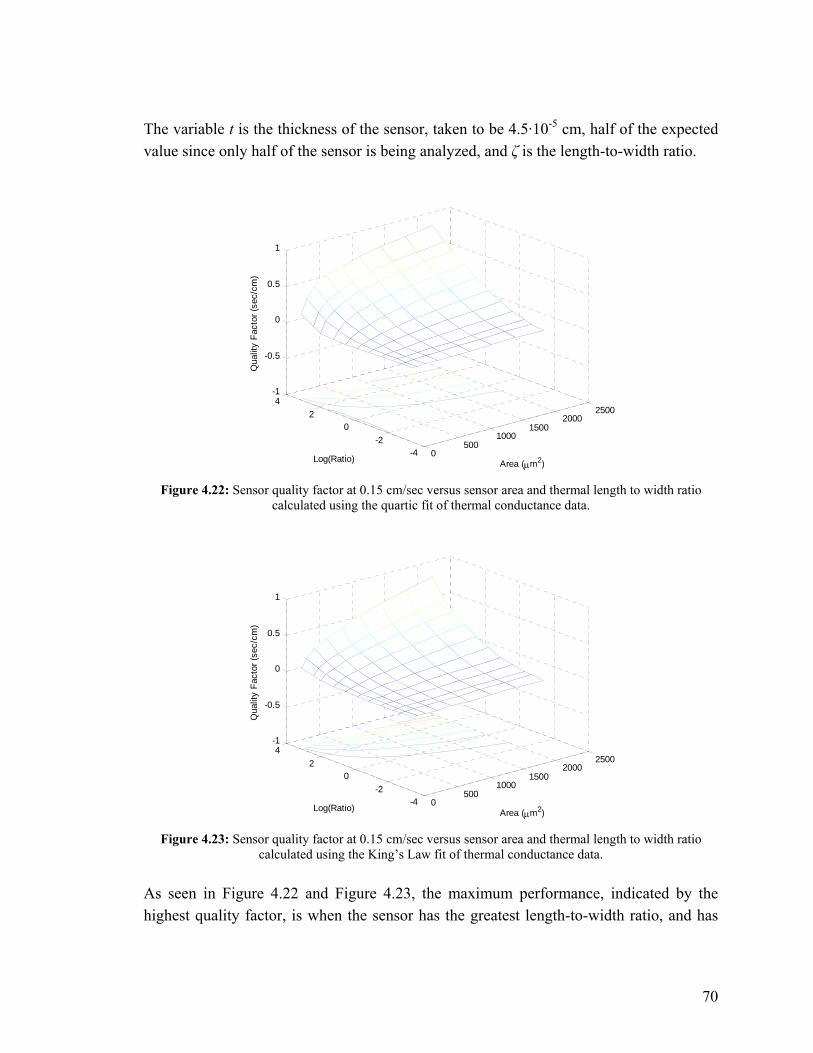
70
The variable t is the thickness of the sensor, taken to be 4.5·10-5 cm, half of the expected value since only half of the sensor is being analyzed, and ζ is the length-to-width ratio.
0500
10001500
20002500
-4-2
02
4-1
-0.5
0
0.5
1
Area (μm2)Log(Ratio)
Qua
lity
Fact
or (s
ec/c
m)
Figure 4.22: Sensor quality factor at 0.15 cm/sec versus sensor area and thermal length to width ratio
calculated using the quartic fit of thermal conductance data.
0500
10001500
20002500
-4-2
02
4-1
-0.5
0
0.5
1
Area (μm2)Log(Ratio)
Qua
lity
Fact
or (s
ec/c
m)
Figure 4.23: Sensor quality factor at 0.15 cm/sec versus sensor area and thermal length to width ratio
calculated using the King’s Law fit of thermal conductance data. As seen in Figure 4.22 and Figure 4.23, the maximum performance, indicated by the highest quality factor, is when the sensor has the greatest length-to-width ratio, and has
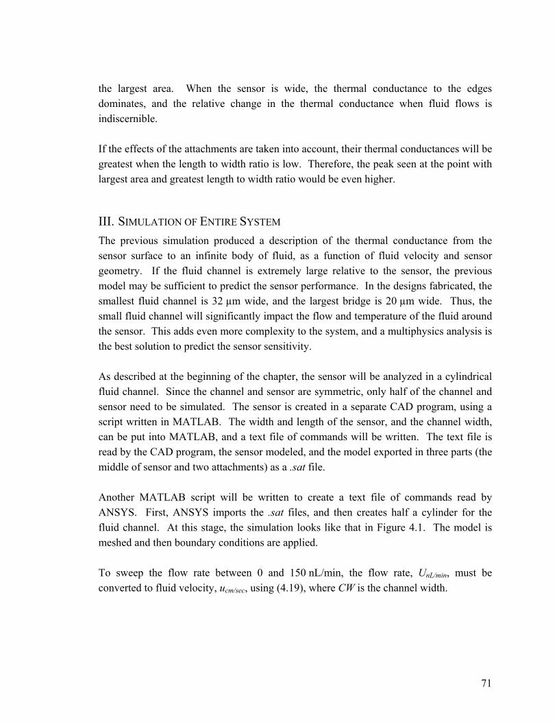
71
the largest area. When the sensor is wide, the thermal conductance to the edges dominates, and the relative change in the thermal conductance when fluid flows is indiscernible. If the effects of the attachments are taken into account, their thermal conductances will be greatest when the length to width ratio is low. Therefore, the peak seen at the point with largest area and greatest length to width ratio would be even higher.
III. SIMULATION OF ENTIRE SYSTEM The previous simulation produced a description of the thermal conductance from the sensor surface to an infinite body of fluid, as a function of fluid velocity and sensor geometry. If the fluid channel is extremely large relative to the sensor, the previous model may be sufficient to predict the sensor performance. In the designs fabricated, the smallest fluid channel is 32 µm wide, and the largest bridge is 20 µm wide. Thus, the small fluid channel will significantly impact the flow and temperature of the fluid around the sensor. This adds even more complexity to the system, and a multiphysics analysis is the best solution to predict the sensor sensitivity. As described at the beginning of the chapter, the sensor will be analyzed in a cylindrical fluid channel. Since the channel and sensor are symmetric, only half of the channel and sensor need to be simulated. The sensor is created in a separate CAD program, using a script written in MATLAB. The width and length of the sensor, and the channel width, can be put into MATLAB, and a text file of commands will be written. The text file is read by the CAD program, the sensor modeled, and the model exported in three parts (the middle of sensor and two attachments) as a .sat file. Another MATLAB script will be written to create a text file of commands read by ANSYS. First, ANSYS imports the .sat files, and then creates half a cylinder for the fluid channel. At this stage, the simulation looks like that in Figure 4.1. The model is meshed and then boundary conditions are applied. To sweep the flow rate between 0 and 150 nL/min, the flow rate, UnL/min, must be converted to fluid velocity, ucm/sec, using (4.19), where CW is the channel width.

72
2
6
min/sec/
260
10
⎟⎠⎞
⎜⎝⎛⋅
=−
CWUu nLcm
π
(4.19)
The fluid velocity is constrained at the inlet, and at the outlet, zero pressure is applied. Zero pressure serves only as a reference. The difference in pressure between the inlet and outlet is the only figure of interest, but the simulation is underconstrained without the pressure defined at some point. A flow velocity of zero is applied along the half-cylinder defining the fluid channel, forcing no slippage. The temperature is held at 310°K, which is approximately body temperature, along the half-cylinder. This way, the substrate acts as a heat sink, which is essentially true given its high thermal conductance and mass. To model the Joule heating due to electrical current, heat generation of 100 mW is applied to the narrow portion of the sensor. An applied power of 1 mW is tested, but the change in temperature is very small. By increasing the power to 100 mW, a larger change in temperature is measured, improving the accuracy of the conductance calculation. Since the density of heat generation, and not the total, must be applied, it is calculated as power divided by volume, Q/V, using (4.20), where W, L, and t are the sensor width, length, and thickness.
2
000,000,1
2
100tLW
serg
tLWmW
VQ
⋅⋅=
⋅⋅= (4.20)
The simulation is run for each width, length, and channel width that is fabricated, at six flow rates between 0 and 150 nL/min. The temperature and fluid velocity results are plotted in ANSYS.
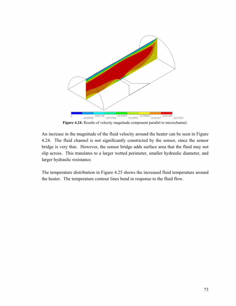
73
Figure 4.24: Results of velocity magnitude component parallel to microchannel.
An increase in the magnitude of the fluid velocity around the heater can be seen in Figure 4.24. The fluid channel is not significantly constricted by the sensor, since the sensor bridge is very thin. However, the sensor bridge adds surface area that the fluid may not slip across. This translates to a larger wetted perimeter, smaller hydraulic diameter, and larger hydraulic resistance. The temperature distribution in Figure 4.25 shows the increased fluid temperature around the heater. The temperature contour lines bend in response to the fluid flow.

74
Figure 4.25: Results of temperature distribution in the fluid.
On just the sensor, the temperature contour in Figure 4.26 can be seen, where the temperature is a maximum on the narrow portion of the sensor, and approaches ambient temperature towards the channel wall.
Figure 4.26: Temperature distribution on entire sensor and heating element.
The temperature of the elements that comprise the heater, seen on the right side of Figure 4.26, are written to a text file. Another set of simulations is performed with the fluid channel removed, so only the conductance directly to the substrate through the attachments can be determined and isolated. The relationship between the total thermal conductance, Gtotal, to the fluid and substrate and the flow rate can be determined. The trend should be similar to that defined by

75
King’s Law in (4.7), but will also include the thermal conductance to the channel wall. Gconvec0 is replaced with aG, and the velocity-dependent component is made a function of the volumetric flow rate, U, instead of the fluid velocity, since the average velocity will be different for different channel widths. The modified form of King’s Law is in (4.21). χUbaG GGtotal += (4.21) The total thermal conductance, is calculated from the heat generation and overheat temperature in the simulations. A typical trend is shown in Figure 4.27.
0 50 100 1501222
1223
1224
1225
1226
1227
1228
Flow Rate nL/min
Ther
mal
Con
duct
ance
(erg
/sec
/°K
)
Figure 4.27: Total thermal conductance vs. flow rate for ANSYS simulations.
The heat transfer due to conduction and velocity independent convection is removed by subtracting the conductance at zero-flow, G(U=0). This represents the parameter, aG, in the King’s law expression: ( )0== UG Ga (4.22) Figure 4.28 shows a typical trend of the fluid velocity-dependent portion of the thermal conductance.

76
0 50 100 1500
1
2
3
4
5
6
Flow Rate nL/min
Ther
mal
Con
duct
ance
(erg
/sec
/°K
)
Figure 4.28: Velocity dependent thermal conductance vs. flow rate
Using only the velocity-dependent data in Figure 4.28, the least-square error trend is obtained using (4.23), (4.24), and (4.25), where U is the flow rate, G is the thermal conductance, χ is the exponent in (4.21), and n is the total number of indices in the summation ([1]).
( ) ( ) ( )
( ) ( )∑ ∑
∑∑∑
= =
===
⎟⎠
⎞⎜⎝
⎛−
−⋅=
n
i
n
iii
n
ii
n
ii
n
iii
UUn
GUGUn
1
2
1
2
111
lnln
lnlnlnlnχ (4.23)
( ) ( )
n
UGn
ii
n
ii ∑∑
==
−=Β 11
lnln χ (4.24)
Β= ebG (4.25) The data point of zero thermal conductivity at zero flow rate is excluded from the calculation, since the natural log of zero is undefined. This data point is taken into account in the definition of the power-law trend.

77
The simulation results of the sensors in each of the fluid channels can be analyzed using a MATLAB script. For the narrowest fluid channel, the experimental results and fitted trends are shown in Figure 4.29. Figure 4.29 shows the relative change in thermal conductance, which is more indicative of the sensitivity versus power consumption than the actual values thermal conductance. The relative thermal conductance is calculated using (4.26), where Gconvec0 is the conductance due to convection at zero flow rate, from the fourth column in Table 4.4.
0
_convec
Grelativeconvec G
UbGχ
= (4.26)
The conductance to the fluid at zero flow rate and to the substrate are shown in Table 4.4, along with the values of bG and χ for the King’s Law fit.
Table 4.4: Results of Simulation with 32 µm Fluid Channel
W L Conduction (erg/sec/°K)
Convection at u=0 (erg/sec/°K) bG*1000 χ R2
4 30 101.6674 918.7 0.0258 2.2142 0.9969 8 30 125.085 1622 0.0084 2.4843 0.9791 16 30 134.5583 2229.4 0.1626 1.8501 0.9997 4 8 71.5033 495.7 0.0308 1.9661 0.9999 4 16 73.3349 641.4 0.0339 2.0688 0.9997 8 16 85.1251 771 0.0701 1.9258 0.9996 16 16 92.3885 972.6 0.1319 1.8342 0.9989

78
0 50 100 1501
1.0005
1.001
1.0015
1.002
1.0025
Flow Rate (nL/min)
Rel
ativ
e C
hang
e in
The
rmal
Con
duct
ance
W =4 L =8 Offset =495.6824 R2 =0.99993
W =4 L =16 Offset =641.4359 R2 =0.99967
W =4 L =30 Offset =918.7496 R2 =0.9969
W =8 L =16 Offset =770.966 R2 =0.99964
W =8 L =30 Offset =1622.0275 R2 =0.97909
W =16 L =16 Offset =972.6276 R2 =0.99888
W =16 L =30 Offset =2229.439 R2 =0.99967
Figure 4.29: Velocity dependent thermal conductance for sensors in a 32 µm fluid channel.
In Table 4.4, the value used for the length of the longest sensor is not equal to the channel width, but is 2 µm shorter, creating short tapered attachments. This is done only so that area numbering in different ANSYS models is consistent, and the simulations can be automated. For example, if the narrow part of the sensor connects directly to the channel walls, and there are no tapered attachments, the numbered areas on which the temperature constraints must be applied are different. However, if there are tapered attachments, no matter what size, the area numbers on which various constraints are placed are consistent. The most interesting feature of the King’s Law fit to the simulation of the sensor in the fluid channel is that the exponent, χ is greater than 1. The mathematical analysis in Chapter 3 predicts that this exponent be ½, and the simulations of the spreading conductance from a rectangle to an infinite body of fluid predict that this exponent is approximately 0.899. Therefore, χ having a value greater than 1, and greater than 2 for some geometries in Table 4.4, is startling. It is possible that this trend is applicable only for the small flow rates tested, and if larger flow rates were simulated, the overall trend may be better fitted with an exponent less than 1. The value of bG is also extremely

79
small, but this is because the flow rate, in nanoliters per minute, and not fluid velocity, is used in (4.21). So, at the maximum flow rate, Uχ is equal to 150χ, which yields values in the tens of thousands. Figure 4.30 and Table 4.5 show the results of the simulation for a 60 µm wide fluid channel. Again, the exponent, χ, suggests a nearly parabolic dependence on flow rate. The narrowest sensor in Figure 4.30 is almost twice as long as the narrowest sensor in Figure 4.29, so both the area and length-to-width ratio should be almost twice as much. However, the conductance to the fluid from the smaller sensor is greater, which is contradictory to (4.1). This must be an effect of the introduction of the channel wall into the simulation. The channel wall is held at a constant temperature, and in the narrower fluid channel, the distance from the heater to the channel wall is shorter. Since the general expression for conductance is inversely proportional to the length (i.e. the distance between areas of different temperature), the narrower channel produces greater values of conductance to the fluid.
Table 4.5: Results of Simulation with 60 µm Fluid Channel
W L Conduction (erg/sec/°K)
Convection at u=0 (erg/sec/°K) bG*1000 χ R2
4 58 70.7581 851.8 0.04272 1.8329 0.996 8 58 97.7664 1278.8 0.0212 2.0178 1 12 58 111.0778 1678 0.02071 2.0295 0.9984 4 30 54.5193 516.6 0.01259 1.9693 0.9995 4 20 55.6481 472.9 0.00113 2.3892 0.9905 12 20 70.5503 745.4 0.00456 2.1862 0.9988 12 40 77.1548 925.9 0.01776 1.984 0.9998

80
0 50 100 1501
1.0001
1.0002
1.0003
1.0004
1.0005
1.0006
Flow Rate (nL/min)
Rel
ativ
e C
hang
e in
The
rmal
Con
duct
ance
W =4 L =58 Offset =851.7556 R2 =0.99596
W =8 L =58 Offset =1278.8253 R2 =0.99999
W =12 L =58 Offset =1678.0162 R2 =0.99844
W =4 L =30 Offset =516.6001 R2 =0.99948
W =4 L =20 Offset =472.8818 R2 =0.99052
W =12 L =20 Offset =745.3914 R2 =0.99883
W =12 L =40 Offset =925.9002 R2 =0.9998
Figure 4.30: Velocity dependent thermal conductance for sensors in a 60 µm fluid channel.
Lastly, the simulation results and fitting parameters for the widest fluid channel are shown in Figure 4.31 and Table 4.6.
Table 4.6: Results of Simulation with 100 µm Fluid Channel
W L Conduction (erg/sec/°K)
Convection at u=0 (erg/sec/°K) bG*1000 χ R2
4 98 48.3567 959.8 0.01828 1.8424 0.9976 8 98 74.5201 1271.4 0.0134 1.9536 0.9971 20 98 105.145 1850.9 0.00804 2.107 0.9924 4 20 47.5996 437.9 0.00672 1.7968 0.9992 4 50 42.2772 560.1 0.02432 1.6584 0.9801 20 20 63.5947 888.6 0.00329 2.101 0.9889 20 40 65.3202 989.1 0.00094 2.4085 0.9774

81
0 50 100 1501
1.0001
1.0002
Flow Rate (nL/min)
Rel
ativ
e C
hang
e in
The
rmal
Con
duct
ance
W =4 L =98 Offset =959.775 R2 =0.99762
W =8 L =98 Offset =1271.3972 R2 =0.99713
W =20 L =98 Offset =1850.8831 R2 =0.99235
W =4 L =20 Offset =437.922 R2 =0.99917
W =4 L =50 Offset =560.0968 R2 =0.98007
W =20 L =20 Offset =888.567 R2 =0.98894
W =20 L =40 Offset =989.0821 R2 =0.97744
Figure 4.31: Velocity dependent thermal conductance for sensors in a 100 µm fluid channel.
For the larger fluid channel, the narrowest sensor in Figure 4.31 that stretches across the entire 100 µm fluid channel exhibits a larger thermal conductance than the narrowest sensor in Figure 4.30. This is what would be expected from (4.1), but is the opposite of what is observed when the channel width is increased from 32 µm in Figure 4.29 to 60 µm in Figure 4.30. This may be due to the fact that when the channel width is significantly large, the thermal conductance to the fluid more closely resembles that of the spreading conductance to an infinite body, and the change in distance between the heater and the constant temperature channel wall is not as influential on the thermal conductance as is the change in sensor geometry. For each simulation, the relative change in thermal conductance is much smaller than what is expected. For the sensor in Table 4.6, with length of 50 µm and width of 4 µm, the relative change in thermal conductance over the maximum flow rate is approximately 1.00017. The relative change for the same area and length-to-width ratio calculated using the expanded King’s Law equation in (4.9) is 1.0067. In the simulation of the entire
82
system, the thickness of the sensor is taken into account, but the dominant variation between the two simulations is, undoubtedly, the effect that the fluid channel has on the thermal spreading conductance. To determine the validity of the results in Figure 4.29, Figure 4.30, and Figure 4.31, it may be beneficial to generate a set of simulations to vary the channel width from a size that would resemble an infinite body, down to the widths used, without adjusting the heater geometries. This would reveal if there is a single constraint imposed in the simulation of the entire system that causes it to deviate from the thermal spreading conductance analysis. It will be most beneficial to fabricate the sensors and characterize the actual material properties, such as thermal conductivity. The fabricated sensors can then be driven with a constant power, and the change in temperature observed and used to calculate the thermal conductance versus flow rate, just as was done in ANSYS. If microscale thermal imaging with high resolution is possible, the validity of the constraint stating that the channel wall temperature will remain constant could be evaluated. Using the finite-element analysis presented, two expressions describing the thermal spreading conductance versus fluid velocity are derived. The first involves approximation and modification of the thermal spreading resistance at zero flow rate equation. The second presents a more compact form by expanding King’s Law parameters as functions of sensor area and length-to-width ratio. These expressions can be used to refine the approximations made in the mathematical analysis in Chapter 3, specifically, by replacing (3.21) with (4.6) or (4.9). The finite-element analysis of the sensor within the fluid channel shows that the heat lost to the walls of the fluid channel, and its effect on the fluid velocity profile, may cause the true sensor behavior to differ significantly from that predicted by the approximation to an infinite half-space of fluid. It is possible that the constraints imposed on the simulation will not accurately describe the system, and the results may not be accurate. The characterization of fabricated sensors will be necessary to validate the simulations, and it may be possible to adjust the imposed constraints so that the results match. REFERENCES
[1] Weisstein, Eric W., "Least Squares Fitting--Power Law," From MathWorld-- http://mathworld.wolfram.com/LeastSquaresFittingPowerLaw.html
83
FABRICATION The anemometer is created using fabrication processes available in the RIT Semiconductor and Microsystems Fabrication Laboratory (SMFL). Microelectromechanical systems (MEMS) and microfluidic devices have been created in the past with similar fabrication methods. Using chemical vapor deposition (CVD) processes, wet etching, plasma etching, and i-line lithographic patterning, an original fabrication process is developed to produce a suspended anemometer bridge consisting of encapsulated doped polysilicon with a front-side KOH etched silicon microchannel. The fabrication of variously sized sensor bridges will determine if there is a limit on the size and shape of sensors that may be realizable. The mathematical analysis in Chapter 3 shows that the sensor design with the most efficient tradeoff between sensitivity and power is the narrowest sensor that stretches all the way across the fluid channel. It is suspected that this geometry will also be the most fragile, and may not withstand all the processing steps. On a single mask, test chips with three different size fluid channels are fabricated, with an array of sensor designs in each channel. The resolution of lithographic patterning will determine the minimum sensor width that will be fabricated, and the maximum length is restricted by the channel width. Generally, in the same fluid channel, two sensors will be fabricated with widths two-times and four-times that of the most narrow sensor. Sensors with the shape adjusted to change the length-to-width ratio without changing the area, or vice-versa, are fabricated to resemble the parameter sweeps in Figure 3.12 and Figure 3.13 of Chapter 3.
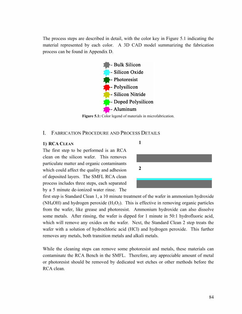
84
The process steps are described in detail, with the color key in Figure 5.1 indicating the material represented by each color. A 3D CAD model summarizing the fabrication process can be found in Appendix D.
Figure 5.1: Color legend of materials in microfabrication.
I. FABRICATION PROCEDURE AND PROCESS DETAILS
1) RCA CLEAN The first step to be performed is an RCA clean on the silicon wafer. This removes particulate matter and organic contaminants which could affect the quality and adhesion of deposited layers. The SMFL RCA clean process includes three steps, each separated by a 5 minute de-ionized water rinse. The first step is Standard Clean 1, a 10 minute treatment of the wafer in ammonium hydroxide (NH4OH) and hydrogen peroxide (H2O2). This is effective in removing organic particles from the wafer, like grease and photoresist. Ammonium hydroxide can also dissolve some metals. After rinsing, the wafer is dipped for 1 minute in 50:1 hydrofluoric acid, which will remove any oxides on the wafer. Next, the Standard Clean 2 step treats the wafer with a solution of hydrochloric acid (HCl) and hydrogen peroxide. This further removes any metals, both transition metals and alkali metals. While the cleaning steps can remove some photoresist and metals, these materials can contaminate the RCA Bench in the SMFL. Therefore, any appreciable amount of metal or photoresist should be removed by dedicated wet etches or other methods before the RCA clean.

85
Standard Clean 1: • 4500 mL H2O • 900 mL H2O2 • 300 mL NH4OH • 75ºC • 10 minutes
HF Dip: • 50:1 H2O:HF • 1 minute
Standard Clean 2: • 4500 mL H2O • 900 mL H2O2 • 300 mL HCl • 75ºC • 10 minutes
2) SILICON OXIDE The first layer deposited is a silicon oxide layer, deposited by plasma-enhanced CVD of tetraethyl orthosilicate (TEOS). This layer was initially designed to be sufficiently thick, on the order of 1 to 1.5 µm, to raise the structure of the sensor above the sacrificial polysilicon deposited to etch the microchannel. Its thickness is reduced to 600 nm, to reduce issues seen by the large, 1 µm step that other layers must conform to. Its remaining purpose is to help insulate layers that generate heat from the substrate. The deposition proceeds by the reaction in (5.1). )(42)( 5222452 OHHCSiOOHHOCSi +→+ (5.1) This layer could just as well be silicon nitride, since it is deposited only for structural purposes, but silicon oxide has a few advantages. The wet-etching of silicon oxide is much faster than silicon nitride (~4 nm/min of silicon nitride in hot phosphoric acid versus ~100 nm/min of silicon oxide in buffered hydrofluoric acid). So for a thick layer, this is a significant difference in etching time. Also, the thermal conductivity of silicon oxide is much lower than silicon nitride, so less of the heat generated by the sensor will be lost to the substrate.
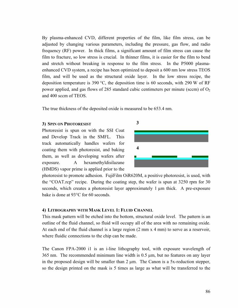
86
By plasma-enhanced CVD, different properties of the film, like film stress, can be adjusted by changing various parameters, including the pressure, gas flow, and radio frequency (RF) power. In thick films, a significant amount of film stress can cause the film to fracture, so low stress is crucial. In thinner films, it is easier for the film to bend and stretch without breaking in response to the film stress. In the P5000 plasma-enhanced CVD system, a recipe has been optimized to deposit a 600 nm low stress TEOS film, and will be used as the structural oxide layer. In the low stress recipe, the deposition temperature is 390 °C, the deposition time is 60 seconds, with 290 W of RF power applied, and gas flows of 285 standard cubic centimeters per minute (sccm) of O2 and 400 sccm of TEOS. The true thickness of the deposited oxide is measured to be 653.4 nm.
3) SPIN ON PHOTORESIST Photoresist is spun on with the SSI Coat and Develop Track in the SMFL. This track automatically handles wafers for coating them with photoresist, and baking them, as well as developing wafers after exposure. A hexamethyldisilazane (HMDS) vapor prime is applied prior to the photoresist to promote adhesion. FujiFilm OiR620M, a positive photoresist, is used, with the “COAT.rcp” recipe. During the coating step, the wafer is spun at 3250 rpm for 30 seconds, which creates a photoresist layer approximately 1 µm thick. A pre-exposure bake is done at 93°C for 60 seconds.
4) LITHOGRAPHY WITH MASK LEVEL 1: FLUID CHANNEL This mask pattern will be etched into the bottom, structural oxide level. The pattern is an outline of the fluid channel, so fluid will occupy all of the area with no remaining oxide. At each end of the fluid channel is a large region (2 mm x 4 mm) to serve as a reservoir, where fluidic connections to the chip can be made. The Canon FPA-2000 i1 is an i-line lithography tool, with exposure wavelength of 365 nm. The recommended minimum line width is 0.5 µm, but no features on any layer in the proposed design will be smaller than 2 µm. The Canon is a 5x-reduction stepper, so the design printed on the mask is 5 times as large as what will be transferred to the

87
wafer. The area allowed on the mask is 100 mm x 100 mm, so the maximum pattern size is 20 mm x 20 mm. The Canon will produce an array of 20 mm x 20 mm patterns across the wafer. The exposure energy used to clear the photoresist is 180 mJ/cm2. Following the exposure, the photoresist is developed using CD-26 positive photoresist developer, and the “DEVELOP.rcp” recipe on the SSI Coat and Develop Track. A post-exposure bake at 112°C is done for 60 seconds. Then, a mixture of de-ionized water and CD-26 is applied to the wafer, allowed to sit for 30 seconds, spun at 700 rpm for 30 seconds, and then spun dry at 2500 rpm for 30 seconds. Lastly, a hard bake at 145°C is done for 60 seconds, which makes the patterned photoresist non-reactive to high energy light.
5) BOE ETCH The buffered oxide etch (BOE), which is primarily hydrofluoric acid, will etch silicon dioxide, but not organic polymers like plastic or photoresist. So, the photoresist can be patterned, and the wafer put into the BOE solution to etch the silicon dioxide. The hydrofluoric acid etch of silicon dioxide follows the chemical reaction in (5.2) ([8]). OHFSiHHFSiO 2622 26 +→+ (5.2)
The buffering action is accomplished by ammonium fluoride (NH4F), which acts to maintain the HF concentration, and also helps to prevent etching of the photoresist. The etch rate for 10:1 (NH4F : 49% HF) BOE can vary depending on how frequently it has been used, and the time since it was last replaced. So, an accurate etch rate should be determined prior to every etch. Typically, on TEOS, the etch rate is on the order of 100 nm/min. For this layer, the TEOS will be etched for 6.5 minutes to include a 10% overetch:
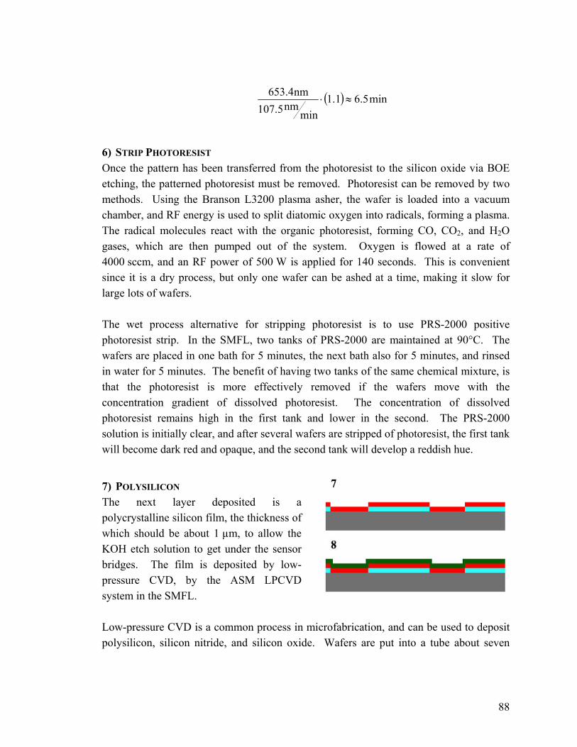
88
( ) min5.61.1min
nm5.107nm4.653
≈⋅
6) STRIP PHOTORESIST Once the pattern has been transferred from the photoresist to the silicon oxide via BOE etching, the patterned photoresist must be removed. Photoresist can be removed by two methods. Using the Branson L3200 plasma asher, the wafer is loaded into a vacuum chamber, and RF energy is used to split diatomic oxygen into radicals, forming a plasma. The radical molecules react with the organic photoresist, forming CO, CO2, and H2O gases, which are then pumped out of the system. Oxygen is flowed at a rate of 4000 sccm, and an RF power of 500 W is applied for 140 seconds. This is convenient since it is a dry process, but only one wafer can be ashed at a time, making it slow for large lots of wafers. The wet process alternative for stripping photoresist is to use PRS-2000 positive photoresist strip. In the SMFL, two tanks of PRS-2000 are maintained at 90°C. The wafers are placed in one bath for 5 minutes, the next bath also for 5 minutes, and rinsed in water for 5 minutes. The benefit of having two tanks of the same chemical mixture, is that the photoresist is more effectively removed if the wafers move with the concentration gradient of dissolved photoresist. The concentration of dissolved photoresist remains high in the first tank and lower in the second. The PRS-2000 solution is initially clear, and after several wafers are stripped of photoresist, the first tank will become dark red and opaque, and the second tank will develop a reddish hue.
7) POLYSILICON The next layer deposited is a polycrystalline silicon film, the thickness of which should be about 1 µm, to allow the KOH etch solution to get under the sensor bridges. The film is deposited by low-pressure CVD, by the ASM LPCVD system in the SMFL. Low-pressure CVD is a common process in microfabrication, and can be used to deposit polysilicon, silicon nitride, and silicon oxide. Wafers are put into a tube about seven

89
inches in diameter, and air is pumped out so that the pressure is on the order of 30-40 millitorr (mT). The tube is heated to a few hundred degrees Celsius, and gases are pumped into the chamber. The high temperature promotes the reaction of the gases on the wafer surface. For polysilicon, silane is pumped into the chamber, and decomposes following the formula in (5.3). 24 2HSiSiH +→ (5.3) The high temperatures required for the deposition can lead to a significant amount of film stress. Since the polycrystalline silicon and bulk silicon should have a very close temperature coefficient of expansion, this is typically not a problem with polysilicon. In films where there is a mismatch between the coefficients of expansion, like with silicon nitride deposited on silicon, the stress can be a major problem, and nitride films thicker than 800 nm may fracture under their own intrinsic stress. For the polysilicon deposition, the chamber is heated to 630 °C, and the silane flow rate is 100 sccm. The tube pressure is maintained at 300 mT. The expected deposition rate is around 11 nm/min.
min90min
nm11nm1000
≈
The deposition will be run for 90 minutes to obtain a 1 µm layer. After the deposition, the polysilicon thickness is measured to be 694.1 nm, considerably less than the expected 1000 nm. As long as the KOH solution will laterally etch the polysilicon film, this thickness should be adequate. The true deposition rate of the 630°C polysilicon recipe is:
minnm7.7
min90nm1.694
=
8) SPIN ON PHOTORESIST
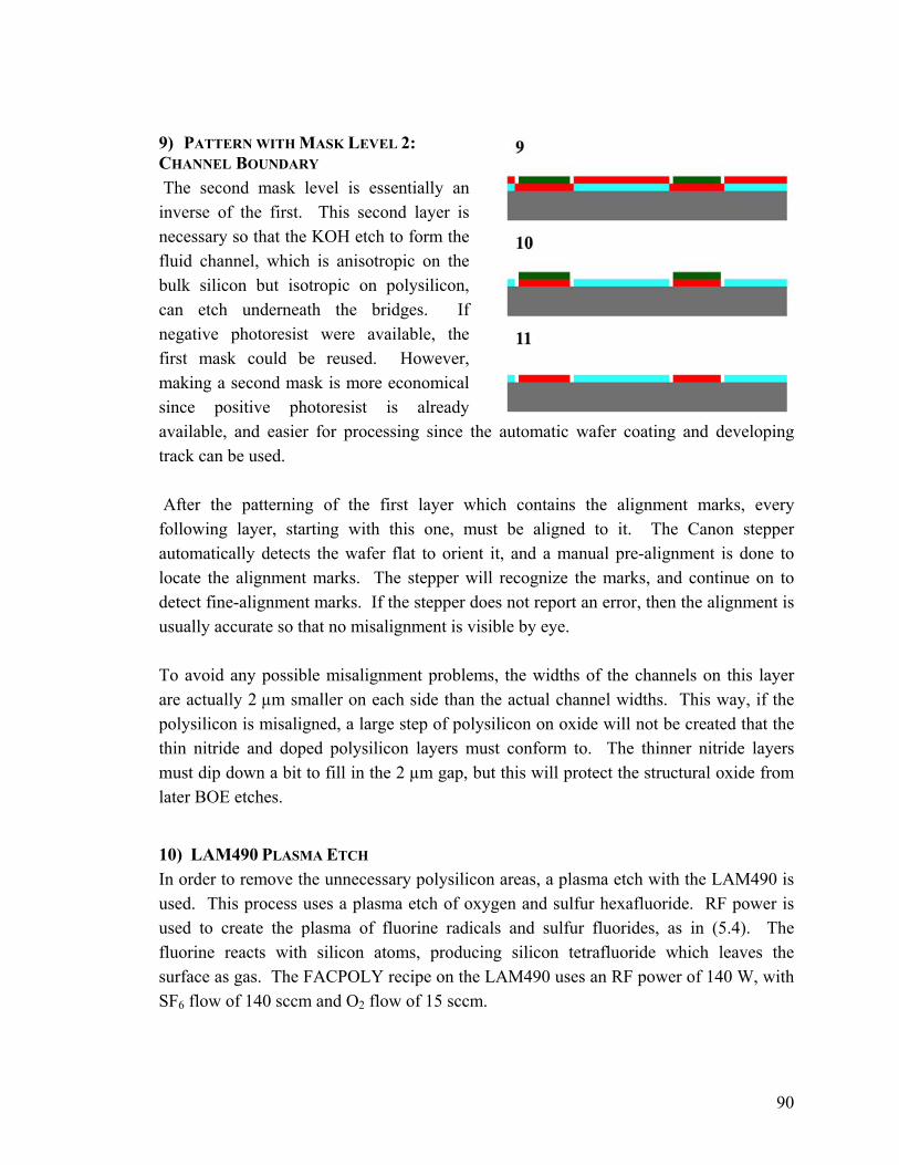
90
9) PATTERN WITH MASK LEVEL 2: CHANNEL BOUNDARY The second mask level is essentially an inverse of the first. This second layer is necessary so that the KOH etch to form the fluid channel, which is anisotropic on the bulk silicon but isotropic on polysilicon, can etch underneath the bridges. If negative photoresist were available, the first mask could be reused. However, making a second mask is more economical since positive photoresist is already available, and easier for processing since the automatic wafer coating and developing track can be used. After the patterning of the first layer which contains the alignment marks, every following layer, starting with this one, must be aligned to it. The Canon stepper automatically detects the wafer flat to orient it, and a manual pre-alignment is done to locate the alignment marks. The stepper will recognize the marks, and continue on to detect fine-alignment marks. If the stepper does not report an error, then the alignment is usually accurate so that no misalignment is visible by eye. To avoid any possible misalignment problems, the widths of the channels on this layer are actually 2 µm smaller on each side than the actual channel widths. This way, if the polysilicon is misaligned, a large step of polysilicon on oxide will not be created that the thin nitride and doped polysilicon layers must conform to. The thinner nitride layers must dip down a bit to fill in the 2 µm gap, but this will protect the structural oxide from later BOE etches.
10) LAM490 PLASMA ETCH In order to remove the unnecessary polysilicon areas, a plasma etch with the LAM490 is used. This process uses a plasma etch of oxygen and sulfur hexafluoride. RF power is used to create the plasma of fluorine radicals and sulfur fluorides, as in (5.4). The fluorine reacts with silicon atoms, producing silicon tetrafluoride which leaves the surface as gas. The FACPOLY recipe on the LAM490 uses an RF power of 140 W, with SF6 flow of 140 sccm and O2 flow of 15 sccm.

91
fluoridessulfurSiFSiSF RF +⎯→⎯+ 46 (5.4) The expected polysilicon etch rate is 8 nm/sec:
sec95sec
nm8Sinm1.694
≈
11) STRIP PHOTORESIST
12) SILICON NITRIDE The first silicon nitride layer will serve as the support for the bridge, and will also cover the structural oxide layer to protect it from later wet etches that attack oxide. The nitride will be about 150 nm thick, and will be deposited by low-pressure CVD or plasma-enhanced CVD. The properties of this layer are particularly important. The stress must not be so high that the bridge will bend, separating the two nitride layers or separating the nitride from the polysilicon comprising the heating element. The film must also be high quality, following a consistent stoichiometry, which is usually Si3N4. This is necessary so that it will withstand later wet etches, particularly the final KOH etch. Deposition by low-pressure CVD will typically produce a higher quality film, since the film growth is limited by chemical reactions on the surface, whereas the film growth rate in plasma-enhanced CVD is controlled by the rate of ions bombarding the surface, not necessarily the type of ion. The low-pressure CVD silicon nitride deposition uses dichlorosilane, as opposed to silane, and ammonia as the source the nitrogen. Dichlorosilane is preferred over silane and other silicon gases because it can produce higher deposition rates at lower temperatures. The SMFL Factory Nitride recipe used performs the deposition at 810°C, with dichlorosilane flowed at 60 sccm and ammonia flowed at 150 sccm. The tube pressure is maintained at 400 mT.

92
Assuming that the stress of the deposited film is due to thermal expansion, and the silicon wafer thickness is much greater than the film thickness, the strain can be predicted by (5.5) ([5]). ( )( )rdsfthermal TT −−= ααε (5.5)
The variable εthermal is the strain due to thermal forces, αf is the temperature coefficient of expansion of the film, and αs is the temperature coefficient of expansion of silicon, Td is the deposition temperature and Tr is room temperature . For an 810°C deposition: ( )( ) 466 1057.3300810106.2103.3 −−− ⋅=−⋅−⋅=thermalε
To find the stress, the strain is multiplied by the modulus of elasticity:
( ) GPa113.0cmdyne1013.1cm
dyne1017.31057.3 29
2124 =⋅=⎟
⎠⎞⎜
⎝⎛ ⋅⋅== −Ethermalthermal εσ
Experimental determination of the film stress in previous SMFL runs have shown the film stress to be approximately 1 GPa. This is in the same range, but quite a lot more than what would be expected due to thermal stress alone, which may be due to other sources of intrinsic stress, and different material properties than those used in calculations. The positive value of the film stress implies that it is tensile, meaning the film will pull on itself. Negative values of film stress correlate to compressive stress, and the film will expand to relieve the compression. The directions of curvature for tensile and compressive film stresses are shown in Figure 5.2.
Figure 5.2: Tensile and compressive wafer bending after deposition of silicon nitride.
To estimate how much the bridges will deflect due to 1 GPa of stress, the radius of curvature of the wafer, and each chip, can be estimated by (5.6) ([2]).
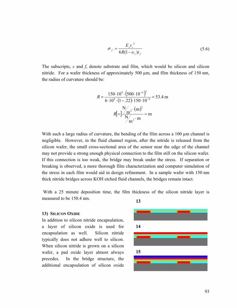
93
fs
ssf tR
tE)1(6
2
υσ
−= (5.6)
The subscripts, s and f, denote substrate and film, which would be silicon and silicon nitride. For a wafer thickness of approximately 500 µm, and film thickness of 150 nm, the radius of curvature should be:
( )( ) m4.53
1015022.11061050010150
99
269
=⋅⋅−⋅⋅
⋅⋅⋅= −
−
R
[ ]( )
mmm
N
mmN
2
22
=⋅
⋅=R
With such a large radius of curvature, the bending of the film across a 100 µm channel is negligible. However, in the fluid channel region, after the nitride is released from the silicon wafer, the small cross-sectional area of the sensor near the edge of the channel may not provide a strong enough physical connection to the film still on the silicon wafer. If this connection is too weak, the bridge may break under the stress. If separation or breaking is observed, a more thorough film characterization and computer simulation of the stress in each film would aid in design refinement. In a sample wafer with 150 nm thick nitride bridges across KOH etched fluid channels, the bridges remain intact. With a 25 minute deposition time, the film thickness of the silicon nitride layer is measured to be 150.4 nm.
13) SILICON OXIDE In addition to silicon nitride encapsulation, a layer of silicon oxide is used for encapsulation as well. Silicon nitride typically does not adhere well to silicon. When silicon nitride is grown on a silicon wafer, a pad oxide layer almost always precedes. In the bridge structure, the additional encapsulation of silicon oxide
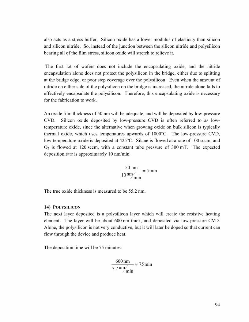
94
also acts as a stress buffer. Silicon oxide has a lower modulus of elasticity than silicon and silicon nitride. So, instead of the junction between the silicon nitride and polysilicon bearing all of the film stress, silicon oxide will stretch to relieve it. The first lot of wafers does not include the encapsulating oxide, and the nitride encapsulation alone does not protect the polysilicon in the bridge, either due to splitting at the bridge edge, or poor step coverage over the polysilicon. Even when the amount of nitride on either side of the polysilicon on the bridge is increased, the nitride alone fails to effectively encapsulate the polysilicon. Therefore, this encapsulating oxide is necessary for the fabrication to work. An oxide film thickness of 50 nm will be adequate, and will be deposited by low-pressure CVD. Silicon oxide deposited by low-pressure CVD is often referred to as low-temperature oxide, since the alternative when growing oxide on bulk silicon is typically thermal oxide, which uses temperatures upwards of 1000°C. The low-pressure CVD, low-temperature oxide is deposited at 425°C. Silane is flowed at a rate of 100 sccm, and O2 is flowed at 120 sccm, with a constant tube pressure of 300 mT. The expected deposition rate is approximately 10 nm/min.
min5min
nm10nm50
=
The true oxide thickness is measured to be 55.2 nm.
14) POLYSILICON The next layer deposited is a polysilicon layer which will create the resistive heating element. The layer will be about 600 nm thick, and deposited via low-pressure CVD. Alone, the polysilicon is not very conductive, but it will later be doped so that current can flow through the device and produce heat. The deposition time will be 75 minutes:
min75min
nm7.7nm600
≈

95
The true thickness is measured to be 544.5 nm.
15) SPIN ON DOPANT FILM A dopant film will serve as the source for the n-type or p-type dopants to be diffused into the polysilicon. For a p-type doping, Borofilm 100 can be used as a source for boron. For n-type, N-250 film can be used for phosphorous. Both solutions are available from Emulsitone Co. The solution is spun-on at a speed of 3000 RPM, and baked at 200°C for 20 minutes. The exact value of the resistivity depends on the dopant film used, as well as the time and temperature of diffusion. A higher temperature and longer bake time will increase the dopant mobility into the silicon, creating a region with lower resistance.
16) DIFFUSE DOPANT INTO POLYSILICON When the dopant film is applied to the wafer and put into the oven, the dopant atoms will diffuse into the silicon. This is usually done at temperatures between 800 and 1200 °C. To prevent damage to the existing structures on the wafer, a low temperature would be preferred. The expected resistivity based on temperature is available from Emulsitone, and the two films are compared in Figure 5.3. As seen from Figure 5.3, the N-250 dopant will provide the lower resistivity, even when diffused for a shorter time. For a low-power, low-voltage system, a low resistance would be preferred. If the resistivity after a single doping is too high, the process can be repeated multiple times to increase the concentration of dopants in the silicon, and further reduce the resistivity. The N250 n-type dopant is applied and diffused at 950°C for one hour. If the process is repeated a second time, a film resistivity of 24 Ω/ is obtained. Figure 5.4 shows a 61-point probe mapping of the resistivity over the wafer after two dopings of N250 film.
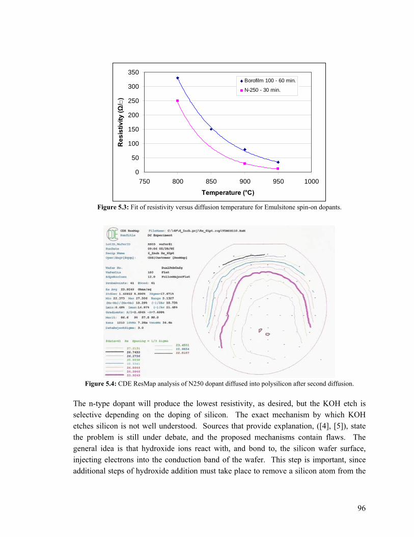
96
The n-type dopant will produce the lowest resistivity, as desired, but the KOH etch is selective depending on the doping of silicon. The exact mechanism by which KOH etches silicon is not well understood. Sources that provide explanation, ([4], [5]), state the problem is still under debate, and the proposed mechanisms contain flaws. The general idea is that hydroxide ions react with, and bond to, the silicon wafer surface, injecting electrons into the conduction band of the wafer. This step is important, since additional steps of hydroxide addition must take place to remove a silicon atom from the
0
50
100
150
200
250
300
350
750 800 850 900 950 1000
Temperature (°C)
Res
istiv
ity (Ω
/)
Borofilm 100 - 60 min.
N-250 - 30 min.
Figure 5.3: Fit of resistivity versus diffusion temperature for Emulsitone spin-on dopants.
Figure 5.4: CDE ResMap analysis of N250 dopant diffused into polysilicon after second diffusion.
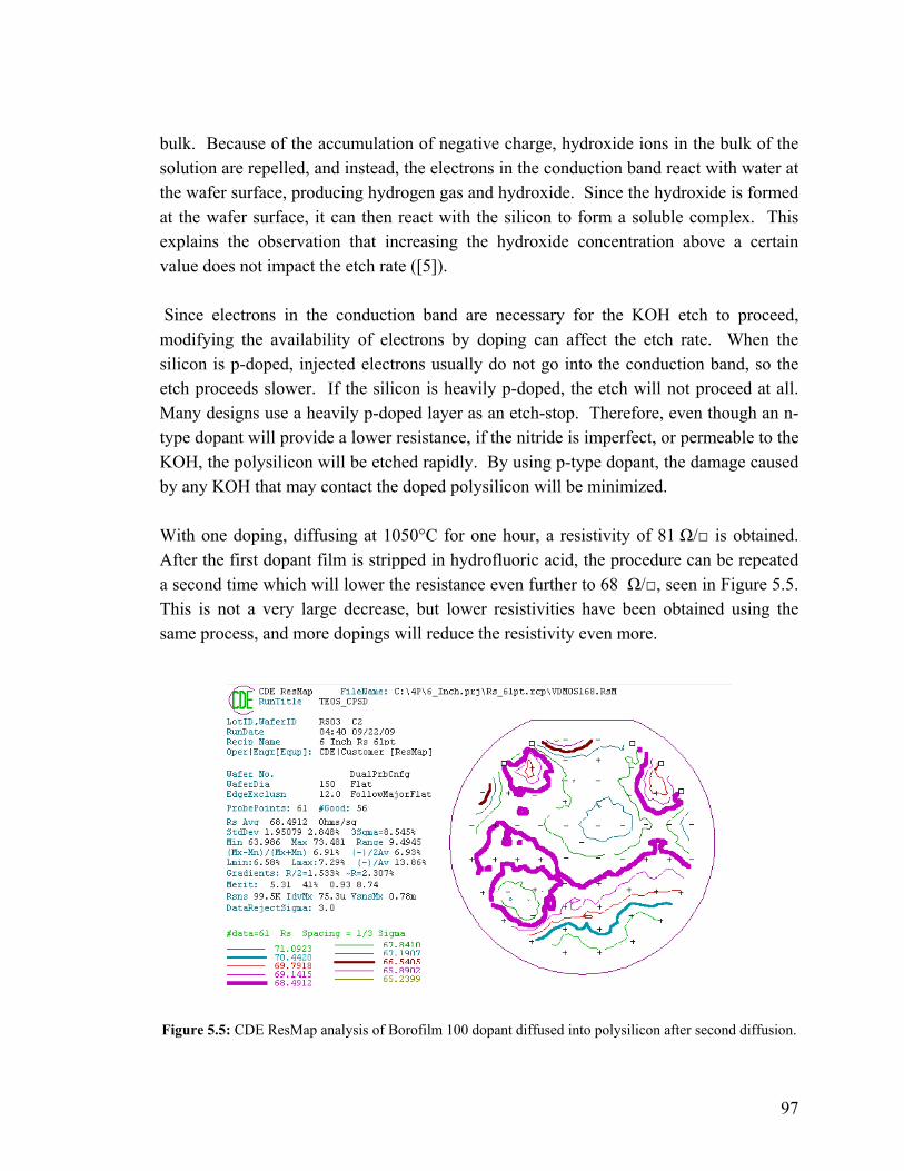
97
bulk. Because of the accumulation of negative charge, hydroxide ions in the bulk of the solution are repelled, and instead, the electrons in the conduction band react with water at the wafer surface, producing hydrogen gas and hydroxide. Since the hydroxide is formed at the wafer surface, it can then react with the silicon to form a soluble complex. This explains the observation that increasing the hydroxide concentration above a certain value does not impact the etch rate ([5]). Since electrons in the conduction band are necessary for the KOH etch to proceed, modifying the availability of electrons by doping can affect the etch rate. When the silicon is p-doped, injected electrons usually do not go into the conduction band, so the etch proceeds slower. If the silicon is heavily p-doped, the etch will not proceed at all. Many designs use a heavily p-doped layer as an etch-stop. Therefore, even though an n-type dopant will provide a lower resistance, if the nitride is imperfect, or permeable to the KOH, the polysilicon will be etched rapidly. By using p-type dopant, the damage caused by any KOH that may contact the doped polysilicon will be minimized. With one doping, diffusing at 1050°C for one hour, a resistivity of 81 Ω/ is obtained. After the first dopant film is stripped in hydrofluoric acid, the procedure can be repeated a second time which will lower the resistance even further to 68 Ω/, seen in Figure 5.5. This is not a very large decrease, but lower resistivities have been obtained using the same process, and more dopings will reduce the resistivity even more.
Figure 5.5: CDE ResMap analysis of Borofilm 100 dopant diffused into polysilicon after second diffusion.
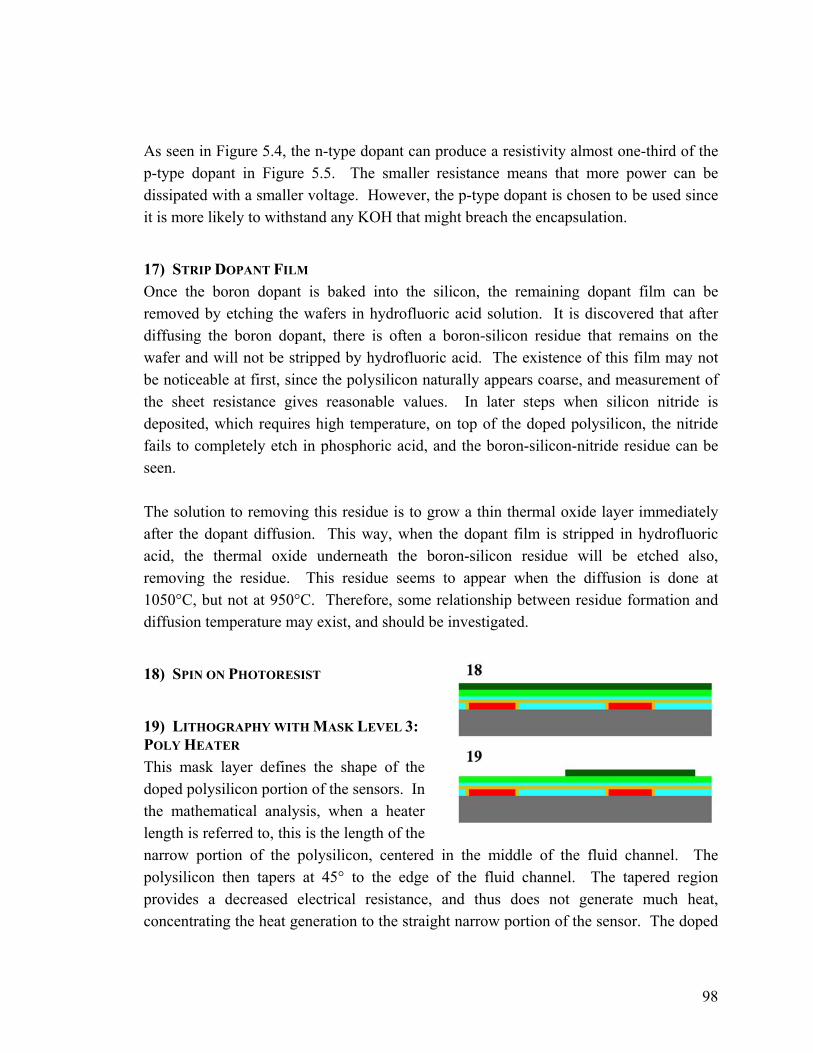
98
As seen in Figure 5.4, the n-type dopant can produce a resistivity almost one-third of the p-type dopant in Figure 5.5. The smaller resistance means that more power can be dissipated with a smaller voltage. However, the p-type dopant is chosen to be used since it is more likely to withstand any KOH that might breach the encapsulation.
17) STRIP DOPANT FILM Once the boron dopant is baked into the silicon, the remaining dopant film can be removed by etching the wafers in hydrofluoric acid solution. It is discovered that after diffusing the boron dopant, there is often a boron-silicon residue that remains on the wafer and will not be stripped by hydrofluoric acid. The existence of this film may not be noticeable at first, since the polysilicon naturally appears coarse, and measurement of the sheet resistance gives reasonable values. In later steps when silicon nitride is deposited, which requires high temperature, on top of the doped polysilicon, the nitride fails to completely etch in phosphoric acid, and the boron-silicon-nitride residue can be seen. The solution to removing this residue is to grow a thin thermal oxide layer immediately after the dopant diffusion. This way, when the dopant film is stripped in hydrofluoric acid, the thermal oxide underneath the boron-silicon residue will be etched also, removing the residue. This residue seems to appear when the diffusion is done at 1050°C, but not at 950°C. Therefore, some relationship between residue formation and diffusion temperature may exist, and should be investigated.
18) SPIN ON PHOTORESIST
19) LITHOGRAPHY WITH MASK LEVEL 3: POLY HEATER This mask layer defines the shape of the doped polysilicon portion of the sensors. In the mathematical analysis, when a heater length is referred to, this is the length of the narrow portion of the polysilicon, centered in the middle of the fluid channel. The polysilicon then tapers at 45° to the edge of the fluid channel. The tapered region provides a decreased electrical resistance, and thus does not generate much heat, concentrating the heat generation to the straight narrow portion of the sensor. The doped
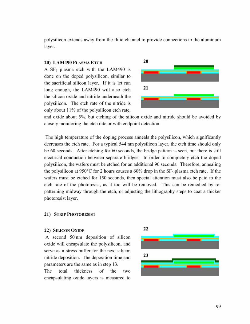
99
polysilicon extends away from the fluid channel to provide connections to the aluminum layer.
20) LAM490 PLASMA ETCH A SF6 plasma etch with the LAM490 is done on the doped polysilicon, similar to the sacrificial silicon layer. If it is let run long enough, the LAM490 will also etch the silicon oxide and nitride underneath the polysilicon. The etch rate of the nitride is only about 11% of the polysilicon etch rate, and oxide about 5%, but etching of the silicon oxide and nitride should be avoided by closely monitoring the etch rate or with endpoint detection. The high temperature of the doping process anneals the polysilicon, which significantly decreases the etch rate. For a typical 544 nm polysilicon layer, the etch time should only be 60 seconds. After etching for 60 seconds, the bridge pattern is seen, but there is still electrical conduction between separate bridges. In order to completely etch the doped polysilicon, the wafers must be etched for an additional 90 seconds. Therefore, annealing the polysilicon at 950°C for 2 hours causes a 60% drop in the SF6 plasma etch rate. If the wafers must be etched for 150 seconds, then special attention must also be paid to the etch rate of the photoresist, as it too will be removed. This can be remedied by re-patterning midway through the etch, or adjusting the lithography steps to coat a thicker photoresist layer.
21) STRIP PHOTORESIST
22) SILICON OXIDE A second 50 nm deposition of silicon oxide will encapsulate the polysilicon, and serve as a stress buffer for the next silicon nitride deposition. The deposition time and parameters are the same as in step 13. The total thickness of the two encapsulating oxide layers is measured to

100
be 102.4 nm.
23) SPIN ON PHOTORESIST
24) LITHOGRAPHY WITH MASK LEVEL 4: OXIDE The silicon oxide will be patterned so that 1 µm of oxide remains on either side of the polysilicon bridge. Contact cuts to the polysilicon are also made so that aluminum traces can make electrical contact to the bridge.
25) BOE ETCH Since the BOE etch is selective to silicon oxide, the etch will stop on the polysilicon for the electrical contacts, and will continue etching down to the silicon nitride in the fluid channel area where there the doped polysilicon has already been removed.
26) STRIP PHOTORESIST
27) SILICON NITRIDE The second silicon nitride layer will complete the double encapsulation of the doped polysilicon. This will prevent the fluid from coming into contact with the conductive polysilicon, which would otherwise could create interaction between the fluid and electricity, such as electrolysis. Silicon nitride is ideal for this outer encapsulation since the etch rate of KOH on silicon nitride is extremely low. This layer will also be about 150 nm, and will be deposited by low-pressure CVD. The total thickness of the two silicon nitride encapsulating layers is 294.4 nm.
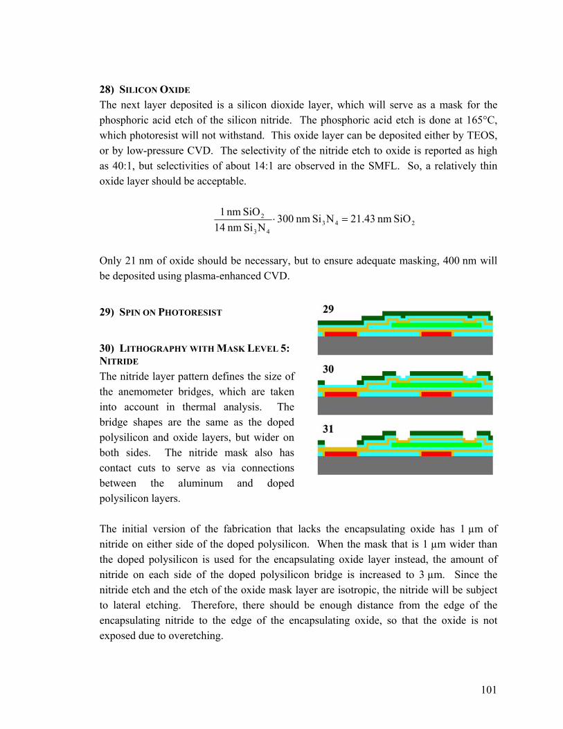
101
28) SILICON OXIDE The next layer deposited is a silicon dioxide layer, which will serve as a mask for the phosphoric acid etch of the silicon nitride. The phosphoric acid etch is done at 165°C, which photoresist will not withstand. This oxide layer can be deposited either by TEOS, or by low-pressure CVD. The selectivity of the nitride etch to oxide is reported as high as 40:1, but selectivities of about 14:1 are observed in the SMFL. So, a relatively thin oxide layer should be acceptable.
24343
2 SiOnm43.21NSinm300NSinm14
SiOnm1=⋅
Only 21 nm of oxide should be necessary, but to ensure adequate masking, 400 nm will be deposited using plasma-enhanced CVD.
29) SPIN ON PHOTORESIST
30) LITHOGRAPHY WITH MASK LEVEL 5: NITRIDE The nitride layer pattern defines the size of the anemometer bridges, which are taken into account in thermal analysis. The bridge shapes are the same as the doped polysilicon and oxide layers, but wider on both sides. The nitride mask also has contact cuts to serve as via connections between the aluminum and doped polysilicon layers. The initial version of the fabrication that lacks the encapsulating oxide has 1 µm of nitride on either side of the doped polysilicon. When the mask that is 1 µm wider than the doped polysilicon is used for the encapsulating oxide layer instead, the amount of nitride on each side of the doped polysilicon bridge is increased to 3 µm. Since the nitride etch and the etch of the oxide mask layer are isotropic, the nitride will be subject to lateral etching. Therefore, there should be enough distance from the edge of the encapsulating nitride to the edge of the encapsulating oxide, so that the oxide is not exposed due to overetching.

102
31) BOE ETCH An etch with hydrofluoric acid solution will remove the silicon dioxide where no photoresist is present. To etch 400 nm of plasma-enhanced CVD oxide will take 3:30 minutes. Since both the HF and hot phosphoric acid etches are isotropic, it is important that the mask not be significantly overetched. With significant lateral etching, the polysilicon and oxide encapsulated by the nitride could be exposed.
32) STRIP PHOTORESIST
33) HOT PHOSPHORIC ACID ETCH Treating the wafers with hot phosphoric acid will selectively etch silicon nitride. The reaction that takes place is described by (5.7). Sundaram in [7] suggests that in the reaction, water hydrolyzes the silicon nitride to form ammonia. This suggests that when the sensor is exposed to the fluid when measuring its velocity, the silicon nitride will slowly dissolve. However, silicon nitride has been commonly used in microfluidic devices without issue. Thus, water hydrolyzing the silicon nitride is most likely only an issue around the temperature and pH ranges of the phosphoric acid etch solution. 3243443243 9)(44273 SiOHPONHPOHOHNSi +→++ (5.7) The selectivity of the phosphoric acid etch is necessary since the etch must stop on the doped polysilicon in some areas, and on the sacrificial polysilicon in others, which occur at different nitride depths. If a plasma etch were used, the doped polysilicon at the contact cuts would be completely destroyed before all of the necessary nitride was etched. The expected etch rate for silicon nitride is around 4 nm/min, and the etch rate of polysilicon is expected to be less than 0.1 nm/min ([9]). So, the doped polysilicon should withstand the entire time of the etch, and underetching at the contacts or at the bridges should not be a problem.

103
Measuring on a test wafer, the silicon nitride in hot phosphoric acid etch rate is found to be 5.5 nm/min:
( ) min 601.1min
nm5.5nm 4.294
≈⋅
After being etched for 60 minutes, much of the nitride over the contacts and in the reservoir areas is cleared, but many sections in the channel between bridges are a different color than the cleared regions, indicating there is remaining nitride. Other areas between bridges have a grainy texture, which indicate that the nitride is being etched, but very unevenly. The most reasonable cause for this behavior is that the high temperature polysilicon doping process further hardens the nitride, or causes the lower nitride and oxide encapsulating layers to form a type of oxynitride, which is more slowly etched in phosphoric acid than true nitride. The granularity seen may arise from the granularity of the polysilicon transferred to the lower layers. To completely remove the silicon nitride, or what may now partially be oxynitride, the wafers are etched in the hot phosphoric acid for periods of 5-10 minutes, and inspected between each etch, until all of the nitride is stripped. To remove all of the nitride, it takes an additional 1 hour and 10 minutes, making the total etch time 2 hours and 10 minutes. This amount of overetching should be avoided, but the thickness of the nitride film is much smaller than the patterned features, there is no risk of the doped polysilicon within the bridge being exposed. To avoid this problem of oxynitride formation, each nitride and oxide encapsulating layer could be patterned and etched after its deposition. The tradeoff is that when the polysilicon layer that comprises the heater is doped, the dopant may diffuse through to the sacrificial polysilicon, and when the doped polysilicon layer is etched, the sacrificial polysilicon will also be partially etched. This should not be a problem, but may introduce new topology and other fabrication issues to follow.
34) STRIP MASK OXIDE The masking oxide should be removed next with a buffered oxide etch. The amount of mask oxide etching in the phosphoric acid should only be a fraction of the amount of nitride etched, so stripping the mask should take close to the time it took to pattern, 3.5 minutes.

104
35) SPUTTER ALUMINUM To make connections to the polysilicon that can later be wire-bonded to, aluminum is sputtered on to the chip to serve as the metal layer. This is done with the CVC 601 sputtering tool. The CVC 601 works by creating a DC electric field across argon gas. The argon ionizes, and the ions are accelerated to an aluminum source, knocking aluminum atoms from the source, which hit and adhere to the wafer surface. The DC sputter of aluminum is done at 2000 W, with argon flowing at a rate of 20 sccm. The chamber pressure is maintained at 5 mT. Sputtering for 30 minutes produces an aluminum film approximately 1 µm thick.
36) SPIN ON PHOTORESIST
37) LITHOGRAPHY WITH MASK LEVEL 6: METAL The metal mask layer contains the pattern that will be used to define the traces and pads. All features of this layer are greater than 100 µm. Traces run from the connections to the doped polysilicon layer to large aluminum pads. Wire-bonds can then be made to the pads to connect to off-chip electronics, which is where the control circuitry can be developed and tested.
38) ALUMINUM WET ETCH With the metal layer patterned onto photoresist, the aluminum can patterned by wet etching. The aluminum etching solution is Aluminum Etchant Type A, which is a mixture of nitric acid, acetic acid, phosphoric acid, and water, in a 16:1:1:2 ratio. Different types of the etchant are available, and Type A is recommended for silicon based microelectronics. This combination of acids gives a good selectivity to aluminum. With

105
silicon mixed into the aluminum, a silicon residue can be formed during the etch. With the etching solution heated to 40 °C, this residue is mostly eliminated. The aluminum is cleared after etching for 3 minutes and 40 seconds.
39) STRIP PHOTORESIST
40) SILICON OXIDE Next, a silicon oxide layer is deposited which will serve as a mask for the KOH etch. KOH can be very destructive, not only to silicon, but also to aluminum and other metals. Therefore, masking for the KOH etch should be given thorough consideration. When masking just a silicon wafer, a pinhole in the mask will etch at the silicon, but lateral etching will be very slow as the (111) planes are revealed. When masking aluminum, the etch is isotropic, so a single hole in the mask will allow a very large area to be etched. A polymer called ProTEK available from Brewer Science, Inc. is designed to be spun onto a wafer and baked. After the bake, it will withstand KOH and similar etchants. ProTEK is typically used for masking the entire side of a wafer without patterning. For it to be used to protect select parts of the front side of the wafer against KOH, a process for transferring a pattern to the ProTEK has been investigated. Although a photopatternable version of the ProTEK is available, it is avoided due to expense. The standard ProTEK polymer can be removed by an oxygen plasma, and by a solvent strip or acetone. Both of these will also remove patterned photoresist, so an aluminum mask will be necessary to withstand the ProTEK etch. Oxygen plasma proves to be the better option for patterning the ProTEK, however a rough residue remains even after being in the oxygen plasma for a few minutes. The remaining residue continues to mask against the KOH etch. A sulfur hexafluoride plasma etch is attempted to remove the residue, but does not appear to have any effect. Acetone and solvent strip leave no residue like with the plasma etch, but act so fast that severe underetching is unavoidable. Near the edge of the etch, the remaining

106
ProTEK begins to peel off. Even with a large distance between the fluid channel mask and the aluminum traces, the masking ability of the ProTEK is compromised. For a patterned mask to protect from the KOH, silicon oxide, is the best option. Silicon nitride works as a better mask against KOH, but removing and patterning a nitride mask would end up destroying the nitride bridge as well. The deposition temperature of the low-pressure CVD nitride is above the melting point of aluminum, so a nitride mask will not be possible. Low-temperature oxide and TEOS, each 1 µm thick, are tested as mask materials. After a couple minutes in KOH, the aluminum covered by the low-temperature oxide has several holes in it, and is almost totally destroyed. The TEOS mask performs better, leaving most of the aluminum intact, but etching is observed at the edge of the aluminum. When the TEOS thickness is increased to 3 µm, the TEOS mask layer completely protects the aluminum layer. The P5000 plasma-enhanced CVD system requires a clean process to be run after each micrometer of TEOS deposited, so 3µm of TEOS will be deposited in three steps.
41) SPIN ON PHOTORESIST
42) LITHOGRAPHY WITH MASK LEVEL 7: KOH The final lithography layer is a outline of the fluid channel, but with a narrower opening in the fluid channel. The narrower fluid channel leaves the mask oxide covering the “crease” at the edge of the fluid channel. This crease is where the thin nitride and oxide encapsulating layers must cover a trench, with the sacrificial polysilicon on one side and the structural oxide on the other. If the combination of film stresses and poor step coverage causes the layers to separate, this may create a pathway for KOH solution to attack the doped polysilicon within the bridges. The sacrificial polysilicon will be etched isotropically by KOH, so the entire fluid channel will still be etched, but the edges of the encapsulating layers will not be exposed.

107
43) BOE ETCH A buffered oxide etch is done next to transfer the pattern of the etch mask to the oxide layer. The BOE etch rate is measured to be 93.9 nm/min.
( ) min 351.1min
nm9.93nm 8.3004
≈⋅
44) STRIP PHOTORESIST
45) KOH ETCH With the masking oxide deposited and patterned, the devices can be etched in KOH. The KOH etch is anisotropic on the bulk silicon due to the crystal pattern of the silicon. In 20% KOH solution at 75 °C, the etch rate on the (100) plane is around 1 µm/min, while on the (111) plane it is essentially zero. Selectivities of KOH to (100) silicon versus (111) silicon are usually listed around 400:1. At 75 °C and 20% KOH solution, the etch rate on the silicon oxide mask is expected to be around 3 nm/min, so there should be no risk of the oxide mask not withstanding the etch. As the KOH etches the unmasked (100) surface of the wafer, the (111) planes are revealed, and the etch tapers inward. The angle of the taper is very consistent, and is known to be 54.74°.
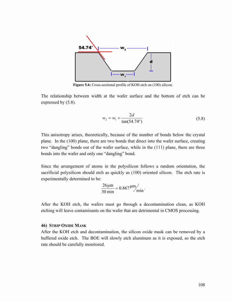
108
Figure 5.6: Cross-sectional profile of KOH etch on (100) silicon.
The relationship between width at the wafer surface and the bottom of etch can be expressed by (5.8).
)74.54tan(2
12 °+=
dww (5.8)
This anisotropy arises, theoretically, because of the number of bonds below the crystal plane. In the (100) plane, there are two bonds that direct into the wafer surface, creating two “dangling” bonds out of the wafer surface, while in the (111) plane, there are three bonds into the wafer and only one “dangling” bond. Since the arrangement of atoms in the polysilicon follows a random orientation, the sacrificial polysilicon should etch as quickly as (100) oriented silicon. The etch rate is experimentally determined to be:
minμm867.0
min30μm26
= .
After the KOH etch, the wafers must go through a decontamination clean, as KOH etching will leave contaminants on the wafer that are detrimental in CMOS processing.
46) STRIP OXIDE MASK After the KOH etch and decontamination, the silicon oxide mask can be removed by a buffered oxide etch. The BOE will slowly etch aluminum as it is exposed, so the etch rate should be carefully monitored.

109
The end result of the sensor fabrication is the doped polysilicon bridge structure, double-encapsulated by silicon oxide and silicon nitride, with aluminum traces and contacts, seen in Figure 5.7.
Figure 5.7: Cross-section of the complete anemometer fabrication process.
II. FABRICATION YIELD If the fabrication process is followed as described, working anemometer bridges are obtained. The first three to four layers of deposition, patterning and etching should proceed smoothly with no signs of incompatibility. Figure 5.8 shows the fabrication progress immediately after step 34. This particular wafer does not have the encapsulating oxide layer, only the nitride. With the encapsulating oxide, the image in Figure 5.8 will appear similarly, but the colors will be different.
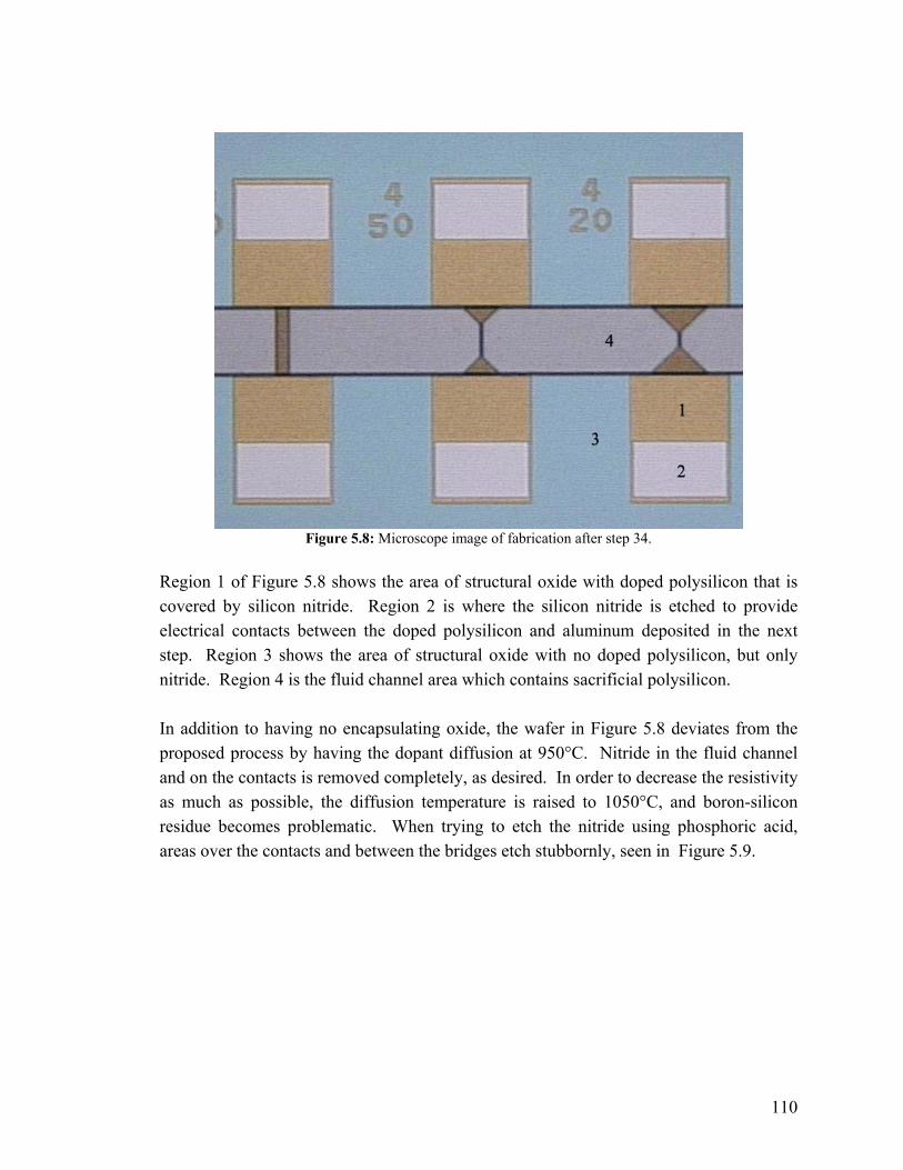
110
Figure 5.8: Microscope image of fabrication after step 34.
Region 1 of Figure 5.8 shows the area of structural oxide with doped polysilicon that is covered by silicon nitride. Region 2 is where the silicon nitride is etched to provide electrical contacts between the doped polysilicon and aluminum deposited in the next step. Region 3 shows the area of structural oxide with no doped polysilicon, but only nitride. Region 4 is the fluid channel area which contains sacrificial polysilicon. In addition to having no encapsulating oxide, the wafer in Figure 5.8 deviates from the proposed process by having the dopant diffusion at 950°C. Nitride in the fluid channel and on the contacts is removed completely, as desired. In order to decrease the resistivity as much as possible, the diffusion temperature is raised to 1050°C, and boron-silicon residue becomes problematic. When trying to etch the nitride using phosphoric acid, areas over the contacts and between the bridges etch stubbornly, seen in Figure 5.9.

111
Figure 5.9: Microscope image of fabrication after step 34 showing residue inhibiting the phosphoric acid
etch. If the wafer is exposed to phosphoric acid long enough, then the residue will be removed. However, lateral etching of the silicon nitride may be significant enough that the encapsulating oxide and polysilicon are exposed. If the residue is left on, it is usually thin enough that it breaks off following the KOH etch, seen in Figure 5.10. The residue does not block the KOH etch of the fluid channel, as sloped sidewalls, which appear as dark blurred bands, can be seen to extend under the residue. The breaking off of residue during processing should not be relied upon when making the final sensor to go in the micropump, as remaining residue could break off, contaminating the drug being dispensed, or clogging the channel downstream from the sensor.
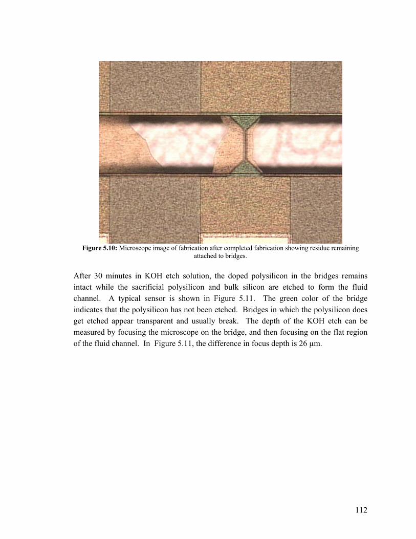
112
Figure 5.10: Microscope image of fabrication after completed fabrication showing residue remaining
attached to bridges. After 30 minutes in KOH etch solution, the doped polysilicon in the bridges remains intact while the sacrificial polysilicon and bulk silicon are etched to form the fluid channel. A typical sensor is shown in Figure 5.11. The green color of the bridge indicates that the polysilicon has not been etched. Bridges in which the polysilicon does get etched appear transparent and usually break. The depth of the KOH etch can be measured by focusing the microscope on the bridge, and then focusing on the flat region of the fluid channel. In Figure 5.11, the difference in focus depth is 26 µm.

113
Figure 5.11: Microscope image showing typical sensor and fluid channel at difference focus depths.
Figure 5.12 shows that even the narrowest sensor that stretches all the way across the fluid channel will withstand the KOH etch and not break. In Figure 5.12, the wafer surface is seen at the top, and the fluid channel is seen in the bottom portion of the image. The bright area in the fluid channel is the bottom surface of the KOH etch, and the dark gradients at the edges are the sloped sidewalls of the etch. On the right side of the sensor, some of the residue discussed with Figure 5.9 can be seen.
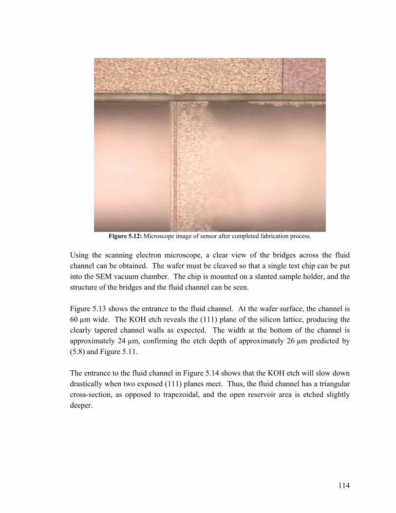
114
Figure 5.12: Microscope image of sensor after completed fabrication process.
Using the scanning electron microscope, a clear view of the bridges across the fluid channel can be obtained. The wafer must be cleaved so that a single test chip can be put into the SEM vacuum chamber. The chip is mounted on a slanted sample holder, and the structure of the bridges and the fluid channel can be seen. Figure 5.13 shows the entrance to the fluid channel. At the wafer surface, the channel is 60 µm wide. The KOH etch reveals the (111) plane of the silicon lattice, producing the clearly tapered channel walls as expected. The width at the bottom of the channel is approximately 24 µm, confirming the etch depth of approximately 26 µm predicted by (5.8) and Figure 5.11. The entrance to the fluid channel in Figure 5.14 shows that the KOH etch will slow down drastically when two exposed (111) planes meet. Thus, the fluid channel has a triangular cross-section, as opposed to trapezoidal, and the open reservoir area is etched slightly deeper.
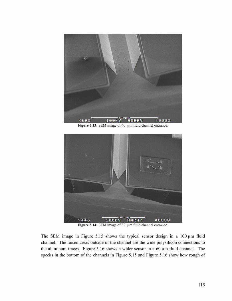
115
Figure 5.13: SEM image of 60 µm fluid channel entrance.
Figure 5.14: SEM image of 32 µm fluid channel entrance.
The SEM image in Figure 5.15 shows the typical sensor design in a 100 µm fluid channel. The raised areas outside of the channel are the wide polysilicon connections to the aluminum traces. Figure 5.16 shows a wider sensor in a 60 µm fluid channel. The specks in the bottom of the channels in Figure 5.15 and Figure 5.16 show how rough of
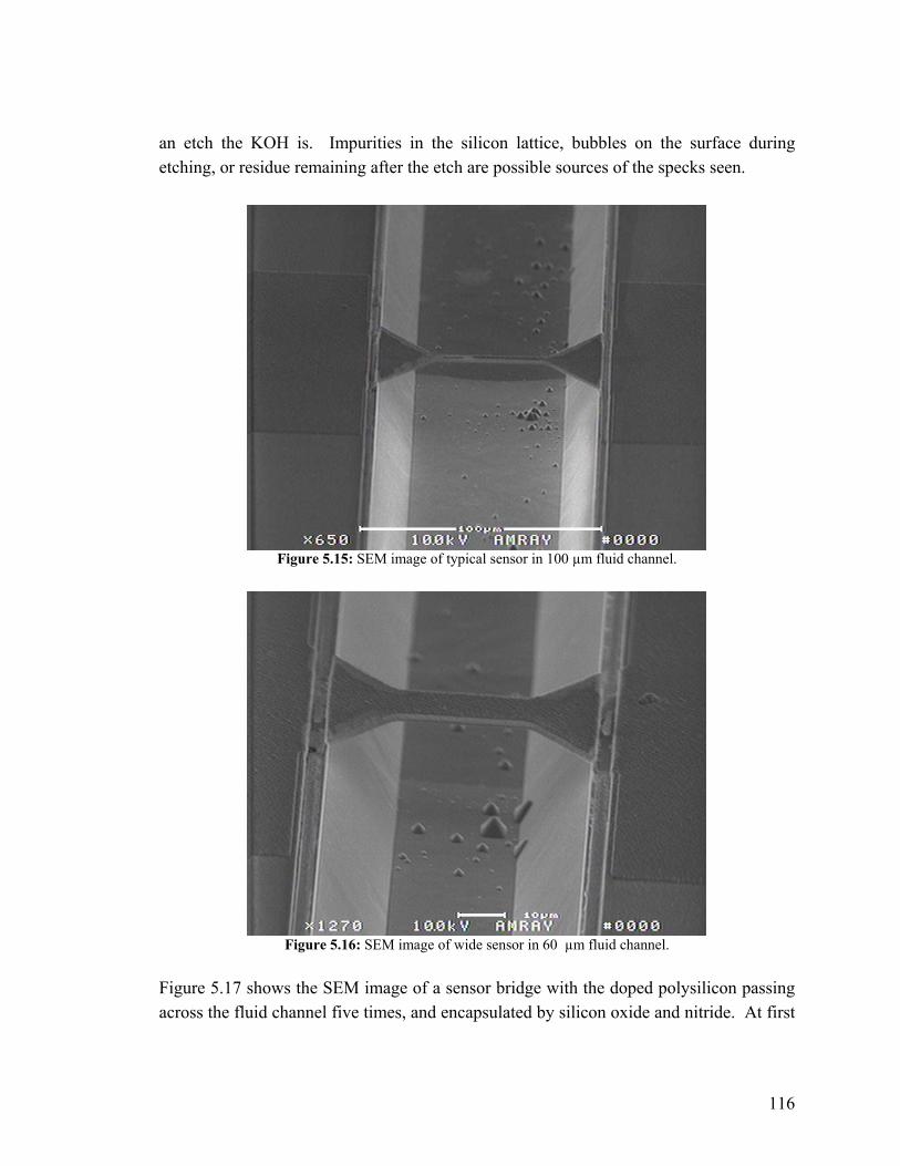
116
an etch the KOH is. Impurities in the silicon lattice, bubbles on the surface during etching, or residue remaining after the etch are possible sources of the specks seen.
Figure 5.15: SEM image of typical sensor in 100 µm fluid channel.
Figure 5.16: SEM image of wide sensor in 60 µm fluid channel.
Figure 5.17 shows the SEM image of a sensor bridge with the doped polysilicon passing across the fluid channel five times, and encapsulated by silicon oxide and nitride. At first

117
glance, the dark regions appear to be sunken areas on the sensor bridge, but the dark area is actually where the doped polysilicon is raised under the silicon nitride.
Figure 5.17: SEM image of encapsulated serpentine polysilicon bridge.
Figure 5.18 shows a close-up of the crease, where the bridge connects to the substrate. This crease is where the deposited films must conform to the steps over the structural oxide and sacrificial polysilicon. This area has caused problems with past fabrication revisions, since the layers are prone to splitting when forced to conform to the small gap. Figure 5.19 shows the complete sensor in the fluid channel with aluminum traces at the far right.
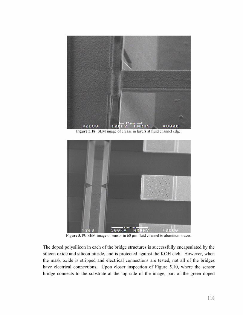
118
Figure 5.18: SEM image of crease in layers at fluid channel edge.
Figure 5.19: SEM image of sensor in 60 µm fluid channel to aluminum traces.
The doped polysilicon in each of the bridge structures is successfully encapsulated by the silicon oxide and silicon nitride, and is protected against the KOH etch. However, when the mask oxide is stripped and electrical connections are tested, not all of the bridges have electrical connections. Upon closer inspection of Figure 5.10, where the sensor bridge connects to the substrate at the top side of the image, part of the green doped

119
polysilicon is noticeably yellow, indicating the doped polysilicon has been etched. This occurs because for this particular wafer, the mask used for the nitride layer does not completely cover the encapsulating oxide layer. Therefore, between etching and stripping the oxide masks used for the phosphoric acid etch and KOH etch, the overetching is enough to breach the encapsulating oxide and expose the doped polysilicon. In bridges where the attachment to the channel wall is very wide, the yield of devices where an electrical connection from one side of the fluid channel to the other can be detected is very high. On a few devices, even the narrowest sensor remains intact and functional, but the yield is very low. Another issue with the final wafer tested is the existence of cross-connections between adjacent bridges. After fabrication step 26, there are no cross-connections, so the doped polysilicon, which is the most likely source of cross-connections, is etched to completion. This particular wafer has had silicon nitride deposited after a layer of aluminum was deposited and stripped for reworking. So, it is suspected that aluminum contaminants remaining on the wafers are able to diffuse under the high temperature of the nitride deposition, creating a conductive layer across the wafer. The resistance between adjacent traces is about 5 kΩ, which is high enough that the sensor bridge will not be shorted out (i.e. the bridge resistance will be lower than the resistance to the neighboring bridges), but high enough that trying to characterize individual sensors with any accuracy may be problematic. REFERENCES
[1] Bean, K.E., “Anisotropic etching of silicon,” Electron Devices, IEEE Transactions on, 1978. 25(10): p. 1185-1193.
[2] Chung, Y.-W., Introduction to Materials Science and Engineering. 1 ed. 2007: CRC/Taylor & Francis.
[3] Franssila, S., Introduction to Microfabrication. 2004: Wiley. [4] Kovacs, G.T.A., N.I. Maluf, and K.E. Petersen, “Bulk micromachining of silicon,”
Proceedings of the IEEE, 1998. 86(8): p. 1536-1551. [5] Madou, M.J., Fundamentals of Microfabrication: The Science of Miniaturization.
2nd ed. 2002: CRC Press. [6] Nguyen, N.-T. and S.T. Wereley, Fundamentals and Applications of Microfluidics.
2nd ed. 2006, Norwood, MA: Artech House.

120
[7] Sundaram, K.B., et al., “Wet etching studies of silicon nitride thin films deposited by electron cyclotron resonance (ECR) plasma enhanced chemical vapor deposition,” 2003, Elsevier Science Ltd. p. 109-114.
[8] Wiberg, N., A.F. Holleman, and E. Wiberg, Inorganic Chemistry. 1 ed. 2001: Academic Press.
[9] Williams, K.R., K. Gupta, and M. Wasilik, “Etch rates for micromachining processing-Part II,” Microelectromechanical Systems, Journal of, 2003. 12(6): p. 761-778.

121
SIGNAL-CONDITIONING CIRCUITRY
From an electrical standpoint, the anemometer bridge is simply a resistor, and its electrical resistance is dependent on temperature. The temperature at which the anemometer stabilizes is dependent on the thermal conductance to the fluid and to the substrate. The thermal conductance, which is proportional to the flow rate, is measured using a control circuit that monitors the change in temperature while the power dissipation is constant, or vice versa. The equation describing the thermal properties of the sensor, (6.1), is derived in Chapter 3:
( ) ( )OHconvecOHsubstrheater
mheater
heater TGTGdt
dTcVRV
⋅⋅+⋅⋅+= 222
ρ .
(6.1) Constant power and constant current anemometers monitor the change in anemometer temperature by the change in resistance. Therefore, when the flow rate changes, the anemometer temperature will rise or fall, and the speed of its response will be dependent on the thermal time constant, which is a function of the heat capacity of the sensor. The thermal time constant, in (6.2), follows the form of resistance times capacitance, common in electrical circuits.
convecsubstr
mthermal GG
cV⋅+⋅
=22
ρτ (6.2)
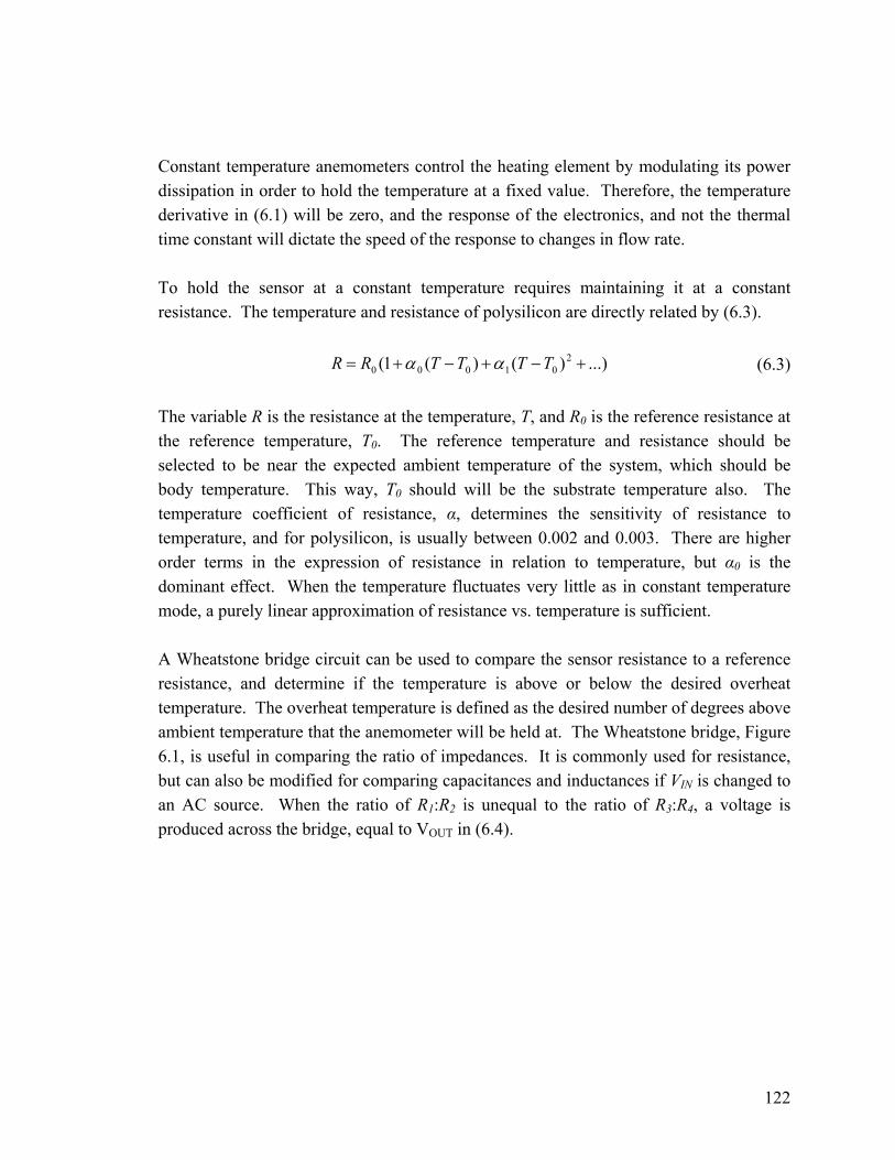
122
Constant temperature anemometers control the heating element by modulating its power dissipation in order to hold the temperature at a fixed value. Therefore, the temperature derivative in (6.1) will be zero, and the response of the electronics, and not the thermal time constant will dictate the speed of the response to changes in flow rate. To hold the sensor at a constant temperature requires maintaining it at a constant resistance. The temperature and resistance of polysilicon are directly related by (6.3). ...))()(1( 2
01000 +−+−+= TTTTRR αα (6.3)
The variable R is the resistance at the temperature, T, and R0 is the reference resistance at the reference temperature, T0. The reference temperature and resistance should be selected to be near the expected ambient temperature of the system, which should be body temperature. This way, T0 should will be the substrate temperature also. The temperature coefficient of resistance, α, determines the sensitivity of resistance to temperature, and for polysilicon, is usually between 0.002 and 0.003. There are higher order terms in the expression of resistance in relation to temperature, but α0 is the dominant effect. When the temperature fluctuates very little as in constant temperature mode, a purely linear approximation of resistance vs. temperature is sufficient. A Wheatstone bridge circuit can be used to compare the sensor resistance to a reference resistance, and determine if the temperature is above or below the desired overheat temperature. The overheat temperature is defined as the desired number of degrees above ambient temperature that the anemometer will be held at. The Wheatstone bridge, Figure 6.1, is useful in comparing the ratio of impedances. It is commonly used for resistance, but can also be modified for comparing capacitances and inductances if VIN is changed to an AC source. When the ratio of R1:R2 is unequal to the ratio of R3:R4, a voltage is produced across the bridge, equal to VOUT in (6.4).
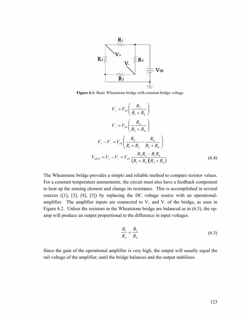
123
Figure 6.1: Basic Wheatstone bridge with constant bridge voltage.
⎟⎟⎠
⎞⎜⎜⎝
⎛+
=+21
2
RRRVV IN
⎟⎟⎠
⎞⎜⎜⎝
⎛+
=−43
4
RRR
VV IN
⎟⎟⎠
⎞⎜⎜⎝
⎛+
−+
=− −+43
4
21
2
RRR
RRRVVV IN
( )( )4321
4132
RRRRRRRRVVVV INOUT ++
−=−= −+ (6.4)
The Wheatstone bridge provides a simple and reliable method to compare resistor values. For a constant temperature anemometer, the circuit must also have a feedback component to heat up the sensing element and change its resistance. This is accomplished in several sources ([1], [3], [4], [5]) by replacing the DC voltage source with an operational-amplifier. The amplifier inputs are connected to V+ and V- of the bridge, as seen in Figure 6.2. Unless the resistors in the Wheatstone bridge are balanced as in (6.5), the op-amp will produce an output proportional to the difference in input voltages.
4
3
2
1
RR
RR
= (6.5)
Since the gain of the operational amplifier is very high, the output will usually equal the rail voltage of the amplifier, until the bridge balances and the output stabilizes.

124
Figure 6.2: Wheatstone bridge with op-amp feedback.
In Figure 6.2, the heating resistor should be in the R4 position, so that if its temperature is too low, the input will be positive, and the output will be high. Since polysilicon has a positive temperature coefficient of resistance, a high voltage at the output will drive current through the bridge to heat R4, raise its temperature, and balance the bridge. This works only if the other resistors in the bridge do not significantly self-heat, which can be accomplished by designing them with a large thermal mass, or situating them on the substrate, which will act as a heat sink. The value of R4 that will make the op-amp stable is given by (6.6).
1
234 R
RRR ⋅= (6.6)
For the maximum sensitivity of the output voltage in (6.4) to changes in R4, the derivative of the sensitivity to R3 can be calculated.
( )( )4321
4132
RRRRRRRR
VV INOUT ++−
=
( )243
3
4 RRR
VdR
dVS IN
OUT
+−
== (6.7)
( ) Smaxat343
43
3
0=+−
=RRRR
dRdS
43 RR =
Setting the derivative of (6.7) to R3 equal to zero shows that the maximum sensitivity occurs when R3 is equal to R4. Since R4 will vary with temperature, R3 will equal the expected value of R4.
125
The heater resistor is put into the R4 position of the Wheatstone bridge, and when taking into account the effect of the temperature, the heater resistance is equal to RH in (6.8).
( )( )1
230004 1
RRRTTRRR HHH ⋅=−+== α (6.8)
TH is the heater temperature, T0 and RH0 are the reference temperature and resistance, and α0 is the temperature coefficient of resistance. The anemometer overheat temperature, TOH, can be calibrated using (6.9).
( )( )( )OHAMBHH TTTRR +−+= 000 1 α
( )00
01
TTR
R
T AMBH
H
OH −−−⎟
⎠⎞⎜
⎝⎛
=α
( )00
10
23 1TT
RRRR
T AMBH
OH −−−⎟
⎠⎞⎜
⎝⎛
=α
. (6.9)
If R3 and R4 are identical, then the fabrication can be made simpler by creating the heating resistor in the fluid channel, and a copy of it outside of the channel. Therefore, assuming the variance of the sheet resistance of the polysilicon is sufficiently small, R3 will equal RH, but while RH heats up, R3 will sink the heat that it generates to the substrate. Therefore, the overheat temperature can adjusted by R2 and R1, as in (6.10).
( )00
1
2 1TT
RR
T AMBOH −−−⎟
⎠⎞⎜
⎝⎛
=α
, (6.10)
TAMB is the ambient temperature of the fluid. For room temperature, ambient temperature is typically 293 °K, and for body temperature, is 310 °K, or 37°C. In constant temperature anemometry, the ambient fluid temperature presents a source of interfering input to the sensor. When the fluid is at a higher temperature, the sensor will produce less heat to reach the overheat temperature, and the output will be indicative of a low thermal conductance, and low flow rate. Ideally, the circuit should operate
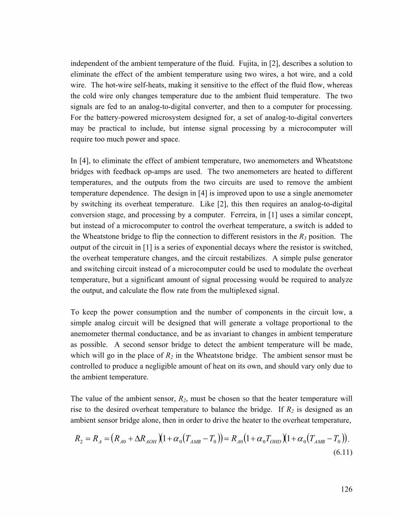
126
independent of the ambient temperature of the fluid. Fujita, in [2], describes a solution to eliminate the effect of the ambient temperature using two wires, a hot wire, and a cold wire. The hot-wire self-heats, making it sensitive to the effect of the fluid flow, whereas the cold wire only changes temperature due to the ambient fluid temperature. The two signals are fed to an analog-to-digital converter, and then to a computer for processing. For the battery-powered microsystem designed for, a set of analog-to-digital converters may be practical to include, but intense signal processing by a microcomputer will require too much power and space. In [4], to eliminate the effect of ambient temperature, two anemometers and Wheatstone bridges with feedback op-amps are used. The two anemometers are heated to different temperatures, and the outputs from the two circuits are used to remove the ambient temperature dependence. The design in [4] is improved upon to use a single anemometer by switching its overheat temperature. Like [2], this then requires an analog-to-digital conversion stage, and processing by a computer. Ferreira, in [1] uses a similar concept, but instead of a microcomputer to control the overheat temperature, a switch is added to the Wheatstone bridge to flip the connection to different resistors in the R3 position. The output of the circuit in [1] is a series of exponential decays where the resistor is switched, the overheat temperature changes, and the circuit restabilizes. A simple pulse generator and switching circuit instead of a microcomputer could be used to modulate the overheat temperature, but a significant amount of signal processing would be required to analyze the output, and calculate the flow rate from the multiplexed signal. To keep the power consumption and the number of components in the circuit low, a simple analog circuit will be designed that will generate a voltage proportional to the anemometer thermal conductance, and be as invariant to changes in ambient temperature as possible. A second sensor bridge to detect the ambient temperature will be made, which will go in the place of R2 in the Wheatstone bridge. The ambient sensor must be controlled to produce a negligible amount of heat on its own, and should vary only due to the ambient temperature. The value of the ambient sensor, R2, must be chosen so that the heater temperature will rise to the desired overheat temperature to balance the bridge. If R2 is designed as an ambient sensor bridge alone, then in order to drive the heater to the overheat temperature,
( ) ( )( ) ( ) ( )( )00000002 111 TTTRTTRRRR AMBOHDAAMBAOHAA −++=−+Δ+== ααα .
(6.11)

127
Here, TOHD is the desired overheat temperature, not to be confused with TOH, which is the actual overheat temperature of the heater bridge . Combining (6.10) and (6.11):
( ) ( )( ) ( )0010
0000 111 TTR
TTTRT AMBAMBOHDA
OH −−−−++
=αα
αα .
If RA0 is chosen to be equal to R1,
( ) ( ) ( )00
0000
11 TTTTTTTTT AMBAMBOHDAMBOHDOH −−−−+−++=α
αα
( )( )001 TTTT AMBOHDOH −+= α (6.12) In (6.12), the dependence on ambient temperature is not completely eliminated. The temperature coefficient of resistance, α0, should be on the order of parts per thousand, so the error is not very large. However, if R2 is split into two separate resistors, one comprised of an ambient sensor bridge, and another outside of the fluid channel representing the ΔRAOH component, then the expression for RA becomes: ( )( ) ( )( ) OHDAAMBAAOHAMBAA TRTTRRTTRR 00000000 11 ααα ⋅+−+=Δ+−+= , (6.13) and the overheat temperature from (6.10) is equal to:
( ) ( ) OHDAMBAMBOHDOH TTTTTTT =−−−−++= 00
00
11αα
. (6.14)
By splitting the ambient sensor component into two elements, a bridge structure which is subject to ambient temperature changes, and a temperature-offsetting resistor outside of the fluid channel, the Wheatstone bridge with feedback op-amp should drive the heater resistor to the desired overheat temperature, independent of the ambient temperature of the fluid. The anemometer control circuit can be simulated using PSPICE simulation software. The thermal behavior of the anemometer can also be simulated in PSPICE by creating a thermal equivalent circuit and coupling it with the electrical circuit. The two coupling equations are the temperature dependence of resistance, (6.3), and Joule heating equation, (6.1).

128
Figure 6.3: Wheatstone bridge electrical circuit in PSPICE. The points RH+ and RH- represent
connections to the thermal equivalent circuit.
Figure 6.4: Anemometer thermal equivalent circuit in PSPICE.
The electrical circuit in Figure 6.3, shows a simple Wheatstone bridge with op-amp feedback. The nodes RH+ and RH- represent connections to the thermal circuit for the heating resistor in Figure 6.4. The 0 V voltage source, heatSense, in Figure 6.4, is used to measure the current through the resistor. The EVALUE block produces a voltage proportional to the current through heatSense. The proportionality (i.e. resistance) is dependent on the temperature on the heater, determined by TH and T0 on the right. The GVALUE block is responsible for transducing electrical power to thermal power.

129
Thermal power, heat, is represented as current in the thermal circuit. The resistive element, R_th, represents the thermal resistance, which will vary with flow rate. The capacitive element, heat_cap, represents the heat capacity of the sensor. The nodes which represent the reference temperature, T0, ambient temperature, TAMB, and heater temperature TH, are indicated on Figure 6.4. For easy integration into more complicated circuits, the thermal equivalent circuit in Figure 6.4 can be reduced to a single circuit element, shown in Figure 6.5. The thermal resistance, heat capacity, and ambient temperature are kept external so that more complex thermal circuits can be evaluated.
Figure 6.5: Heater circuit element coupling electrical circuit and thermal equivalent circuit.
The simplest control circuit with a Wheatstone bridge and op-amp is shown in Figure 6.6. This circuit represents the ideal case in which there is no self-heating of the ambient temperature sensor, caused by the short circuit between T_h and AMB+. The heating element will self-heat and the heat will be dissipated by the thermal circuit with a heat capacity of heat_cap and thermal resistance of R_th. The flow rate changes the thermal resistance of the sensor, so this parameter will be swept when examining the sensitivity to fluid flow. With an ideal operational amplifier, the temperature of the heating element will rise to a value of T_OH, in the leg of the bridge with the ambient sensor. The source voltage, VCC, is 3 Volts.
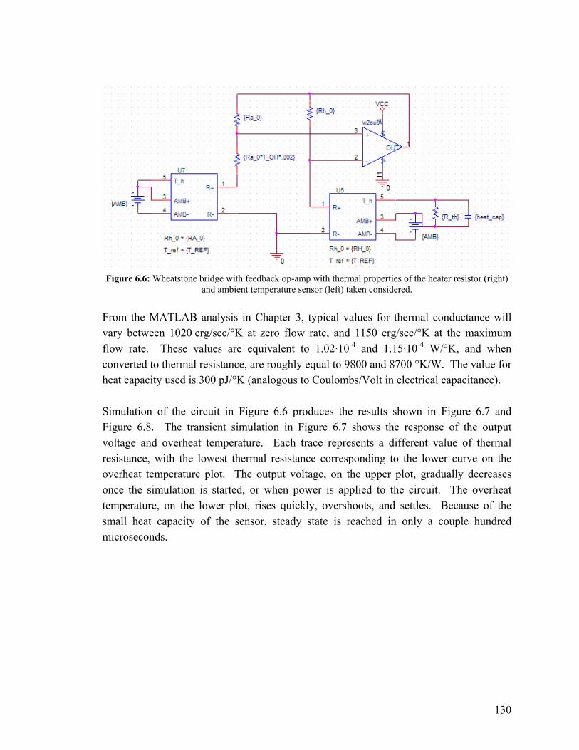
130
Figure 6.6: Wheatstone bridge with feedback op-amp with thermal properties of the heater resistor (right)
and ambient temperature sensor (left) taken considered.
From the MATLAB analysis in Chapter 3, typical values for thermal conductance will vary between 1020 erg/sec/°K at zero flow rate, and 1150 erg/sec/°K at the maximum flow rate. These values are equivalent to 1.02·10-4 and 1.15·10-4 W/°K, and when converted to thermal resistance, are roughly equal to 9800 and 8700 °K/W. The value for heat capacity used is 300 pJ/°K (analogous to Coulombs/Volt in electrical capacitance). Simulation of the circuit in Figure 6.6 produces the results shown in Figure 6.7 and Figure 6.8. The transient simulation in Figure 6.7 shows the response of the output voltage and overheat temperature. Each trace represents a different value of thermal resistance, with the lowest thermal resistance corresponding to the lower curve on the overheat temperature plot. The output voltage, on the upper plot, gradually decreases once the simulation is started, or when power is applied to the circuit. The overheat temperature, on the lower plot, rises quickly, overshoots, and settles. Because of the small heat capacity of the sensor, steady state is reached in only a couple hundred microseconds.
131
Figure 6.7: Transient simulation results of the circuit in Figure 6.6.
Only the steady-state voltage is necessary, so a DC sweep simulation is performed. In Figure 6.8, the primary sweep, along the x-axis, is thermal resistance, and the secondary sweep, shown by separate traces, is ambient temperature. Over the range of expected thermal resistance values, the change in output voltage is approximately -97.75 mV, making the sensitivity -88.8 µV·W/°K (V/(°K/W)). The sensitivity of the overheat temperature to thermal resistance is 4.02 µW (°K/(°K/W)). In Figure 6.8, the x-axis is reversed (i.e. higher values are to the left) to show the trend versus flow rate, since flow rate and thermal resistance are inversely related.
Figure 6.8: DC Sweep simulation results of the circuit in Figure 6.6.

132
The values of RH0 and RA0 in the simulation are 625 Ω. This is approximately the value measured on a fabricated sensor of the nominal geometry in Table 3.4 (LE = 50 µm, WE = 2 µm, CW = 100 µm). If the resistance is too high, the op-amp will not be able to heat the sensor up to the necessary temperature, leaving the bridge unbalanced, and the op-amp output remaining at the rail voltage. Therefore, no signal can be detected. In this scenario, the overheat temperature must be reduced so that the bridge can be balanced with the available voltage. In simulations with resistances other than 625 Ω that do not constantly force the op-amp output to the rail, similar results to those in Figure 6.7 and Figure 6.8 are observed. Reducing the overheat temperature reduces the sensitivity also. If the overheat temperature of the circuit in Figure 6.6 is varied, the results in Figure 6.9 are obtained. The relationship between overheat temperature and sensitivity is quite linear, seen in Figure 6.10.
R_th
9.8K 9.6K 9.4K 9.2K 9.0K 8.8K 8.6K9.9KV(w2outA:OUT)
0.8V
1.2V
1.6V
2.0V
2.4V
Figure 6.9: Results of varying overheat temperature in Figure 6.6.

133
y = -0.0154x + 1.0048
y = -0.0688x + 1.9388
y = -0.0888x + 2.4835
y = -0.1052x + 2.9309
y = -0.1193x + 3.3194
0
0.5
1
1.5
2
2.5
8.599.510
Thermal Resistance (°K/mW)
Volta
ge (V
)
T_OH = 2°KT_OH = 6°KT_OH = 10°KT_OH = 14°KT_OH = 18°K
Figure 6.10: Dependence of circuit sensitivity on overheat temperature.
The overheat temperature will be kept at 10°K, so that the average voltage requirement is not too high, while keeping a reasonable sensitivity. In Figure 6.6, the ambient sensor is given no thermal characteristics, making this scenario the ideal case. If the ambient sensor is given the same thermal properties as the heating element, the circuit in Figure 6.11 is created. If the ambient sensor resistance, RA0, and heater resistance, RH0, are taken to be the same again, the circuit will fail to produce a useful signal, since the ambient sensor and heater will heat symmetrically. Only the temperature-offsetting resistor, with a value of RA0·TOH·0.002, is different between the two bridges, but this small resistor is not enough to limit the current to the ambient sensor. Having the ambient temperature sensor self-heat also causes it to deviate from ambient temperature, negating its intended purpose.
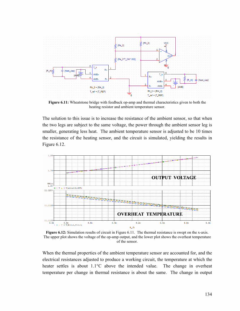
134
Figure 6.11: Wheatstone bridge with feedback op-amp and thermal characteristics given to both the
heating resistor and ambient temperature sensor. The solution to this issue is to increase the resistance of the ambient sensor, so that when the two legs are subject to the same voltage, the power through the ambient sensor leg is smaller, generating less heat. The ambient temperature sensor is adjusted to be 10 times the resistance of the heating sensor, and the circuit is simulated, yielding the results in Figure 6.12.
Figure 6.12: Simulation results of circuit in Figure 6.11. The thermal resistance is swept on the x-axis.
The upper plot shows the voltage of the op-amp output, and the lower plot shows the overheat temperature of the sensor.
When the thermal properties of the ambient temperature sensor are accounted for, and the electrical resistances adjusted to produce a working circuit, the temperature at which the heater settles is about 1.1°C above the intended value. The change in overheat temperature per change in thermal resistance is about the same. The change in output
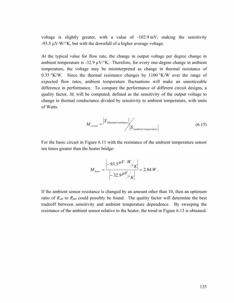
135
voltage is slightly greater, with a value of -102.9 mV, making the sensitivity -93.5 µV·W/°K, but with the downfall of a higher average voltage. At the typical value for flow rate, the change in output voltage per degree change in ambient temperature is -32.9 µV/°K. Therefore, for every one-degree change in ambient temperature, the voltage may be misinterpreted as change in thermal resistance of 0.35 °K/W. Since the thermal resistance changes by 1100 °K/W over the range of expected flow rates, ambient temperature fluctuations will make an unnoticeable difference in performance. To compare the performance of different circuit designs, a quality factor, M, will be computed, defined as the sensitivity of the output voltage to change in thermal conductance divided by sensitivity to ambient temperature, with units of Watts.
etemperaturambient
circuit SS
MΔ
= resistanceΔthermal (6.15)
For the basic circuit in Figure 6.11 with the resistance of the ambient temperature sensor ten times greater than the heater bridge:
W
KV
KWV
M basic 84.29.32
5.93=
°−
°⋅−
=μ
μ
.
If the ambient sensor resistance is changed by an amount other than 10, then an optimum ratio of RA0 to RH0 could possibly be found. The quality factor will determine the best tradeoff between sensitivity and ambient temperature dependence. By sweeping the resistance of the ambient sensor relative to the heater, the trend in Figure 6.13 is obtained.

136
0
0.5
1
1.5
2
2.5
3
3.5
1 10 100 1000 10000
RA0/RH0
Qua
lity
Fact
or (W
)
Figure 6.13: Effect of changing the value of the ambient temperature sensor in Figure 6.11 on quality
factor. Increasing the value of the ambient temperature sensor improves the performance as expected. A maximum value seems to be reached, but there is a wide plateau in the data. So long as the ambient sensor has 100 times larger resistance than the heater, no significant change in performance will be observed. The quality factor starts to decrease at a RA0/RH0 ratio of 2000, but in this range, resistances on the order of megaohms must be dealt with, which noise and fabrication limitations tend to prohibit. A few complications arise when the ambient temperature sensor resistance is increased compared to the heater resistor. In the simulation, the resistance of the ambient temperature sensor is ten times that of the heater resistor. When resistances become very large, the thermal noise that they generate can become an issue. For a ten-fold increase in resistance, the Johnson noise of a resistor will be √10 times as much. This is typically only an issue at high frequencies, since the Johnson noise is dependent on bandwidth. When only the steady state value is of interest, the noise should not be a problem. The greater problem is fabrication. In order to fabricate a resistor with ten times the resistance, the ratio of width to length must be one tenth. In the fabrication design, the width of the heating resistor is close to the minimum resolution of the lithography tool. Therefore, the ambient temperature sensor must be ten times as long instead, and to fit into the flow channel, must cross from one side to the other repeatedly. This introduces complications into fabrication, and raises questions as to whether the bridge encapsulating a meandering polysilicon strip will withstand processing. An encapsulated

137
meandering polysilicon strip passing across the fluid channel five times is successfully fabricated, but if the polysilicon must pass across the fluid channel several more times, unanticipated problems may arise. Sensor bridges in which the doped polysilicon is etched, usually break, indicating that the polysilicon provides most of the mechanical support for the bridge. If the nitride is wide at the edge of the channel, without comparable polysilicon width for mechanical support, the nitride stress in the bridge may cause it to break. To prevent excessive self-heating of the ambient temperature sensor without modifying its resistance, the ambient temperature sensor can be replaced with a circuit to act as a resistance, but ultimately driving less current through the ambient sensor. This “virtual resistor” can be made using a circuit that produces a voltage in response to a current, or a transimpedance circuit. The mathematical logic follows that:
1
11 R
VI =
( ) 10 ITRRV OHAAA ⋅⋅⋅+= α
( )1
02
1
10 R
TRRVRVTRRV OHAA
OHAAAαα ⋅⋅+
⋅=⋅⋅⋅+= .
The variable I1 represents the current through R1 in the Wheatstone bridge diagram, and VA is the voltage across the ambient temperature sensor. The rearranged expression resembles that of an inverting amplifier, only positive. If an inverting amplifier was used, a differential inverting amplifier could be added to make the expression positive. In order to isolate the voltage across R2, a differential amplifier can be used. With a differential amplifier at the front of the circuit, and a second differential amplifier at the end, the gain of these two stages can be adjusted so that the voltage across the ambient temperature sensor is low, reducing the self-heating. The proposed circuit is in Figure 6.14. Each op-amp in Figure 6.14 is a TLC25 (Texas Instruments).

138
Figure 6.14: Wheatstone bridge with feedback amplifier circuit with ambient temperature sensor element
replaced with transimpedance circuit. The equation describing the entire transimpedance circuit follows, and the equivalent impedance, in (6.16), is the same as the original resistance for RA in (6.13).
( )k
kR
TRRk
kRIVA
OHAAARAOUT 1
10101
0
000
−⋅⋅+−⋅⋅=
α
α⋅⋅+= OHAARA
OUT TRRIV
00
(6.16)
As seen, the transimpedance of the circuit is the same as in bottom left element of Figure 6.11. However, by stepping down the voltage across the ambient sensor, self-heating is reduced without having to increase the resistance. Within the transimpedance circuit, the reference voltage is changed from ground to a virtual ground, VGND, that is held half-way between ground and the source voltage. The other ground voltage points are changed to a PGND, at 0.5 V, so that none of the op-amps are forced to produce an output near the rail voltage. The values of the 1 kΩ and 10 kΩ resistors of the amplifiers could just as well be 1 MΩ and 10 MΩ, since only the ratio of the two is important, not the exact values. The results of the simulation are shown in Figure 6.15.
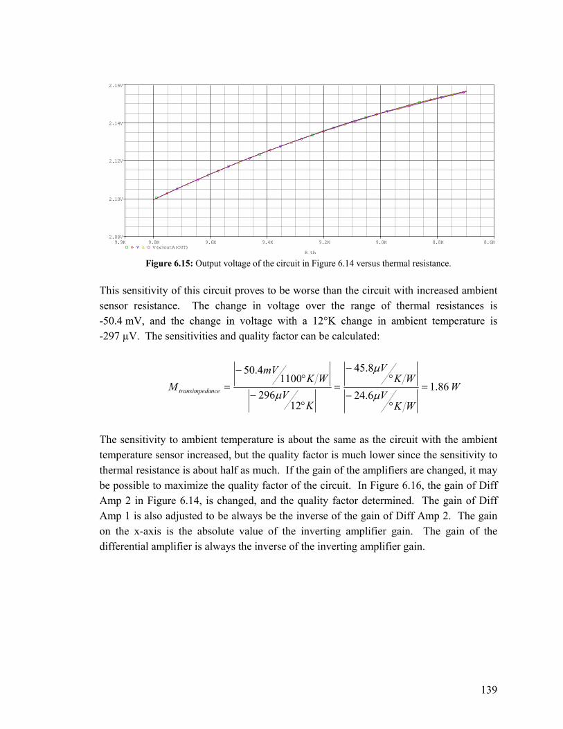
139
R th
9.8K 9.6K 9.4K 9.2K 9.0K 8.8K 8.6K9.9KV(w3outA:OUT)
2.08V
2.10V
2.12V
2.14V
2.16V
Figure 6.15: Output voltage of the circuit in Figure 6.14 versus thermal resistance.
This sensitivity of this circuit proves to be worse than the circuit with increased ambient sensor resistance. The change in voltage over the range of thermal resistances is -50.4 mV, and the change in voltage with a 12°K change in ambient temperature is -297 µV. The sensitivities and quality factor can be calculated:
W
WKV
WKV
KV
WKmV
M ancetransimped 86.16.24
8.45
12296
11004.50
=
°−
°−
=
°−
°−
=μ
μ
μ
The sensitivity to ambient temperature is about the same as the circuit with the ambient temperature sensor increased, but the quality factor is much lower since the sensitivity to thermal resistance is about half as much. If the gain of the amplifiers are changed, it may be possible to maximize the quality factor of the circuit. In Figure 6.16, the gain of Diff Amp 2 in Figure 6.14, is changed, and the quality factor determined. The gain of Diff Amp 1 is also adjusted to be always be the inverse of the gain of Diff Amp 2. The gain on the x-axis is the absolute value of the inverting amplifier gain. The gain of the differential amplifier is always the inverse of the inverting amplifier gain.

140
0
0.5
1
1.5
2
2.5
1 10 100 1000 10000
Gain of Diff Amp 2 (V/V)
Qua
lity
Fact
or (W
)
Figure 6.16: Effect of changing amplifier gain of Diff Amp 2 in the circuit in Figure 6.14 on quality factor. Clearly there is a maximum between gains of 10 and 100. Focusing on this maximum, the plot in Figure 6.17 is obtained. A maximum quality factor is obtained with a gain at about 28 V/V.
2.05
2.1
2.15
2.2
2.25
2.3
2.35
2.4
10 100
Gain of Diff Amp 2 (V/V)
Qua
lity
Fact
or (W
)
Figure 6.17: Amplifier gain of Diff Amp 2 in the circuit in Figure 6.14 to produce maximum quality factor. The downfall of this design is that many more op-amps are introduced into the circuit, which will greatly increase the power consumption and size. According the simulation, if

141
a TLC25 op-amp is used, which is designed for low power, each op-amp consumes about 2.5 mW. If five additional op-amps are used, approximately 12.5 mW are added to the power consumption. Other solutions where stepping down the voltage across the ambient temperature sensor with fewer op-amps may be possible. Instead of trying to replace only the ambient temperature sensor with a transimpedance feedback circuit as in Figure 6.14, the entire side of the Wheatstone bridge can be modified.
Figure 6.18: Wheatstone bridge with feedback amplifier and ambient side voltage reduction.
By moving the amplifiers to the top and bottom of the Wheatstone bridge, the differential amplifier and additional inverting amplifier in Figure 6.14 can be removed. Instead, a voltage divider with unity gain amplifier and non-inverting amplifier can be used, seen in Figure 6.18. This circuit also does not need a virtual ground, since the voltage signal is not inverted. In this circuit also, the values of the resistors in the amplifiers are not critical, only the ratio. The results of the simulation are shown in Figure 6.19.

142
R th
9.8K 9.6K 9.4K 9.2K 9.0K 8.8K 8.6K9.9KV(R44:2)
2.204V
2.208V
2.212V
2.216V
Figure 6.19: Output voltage of the circuit in Figure 6.18 versus thermal resistance with different ambient
temperatures. The magnitude of the sensitivity is reduced significantly to -6.76 µV·W/°K. The change in voltage with a 12°K change in ambient temperature is -381.7 µV, another decrease in performance compared to the previous circuit. The quality factor is calculated to be:
W
KV
WKV
KV
WKmV
M downstep 212.081.31
76.6
127.381
1100445.7
=
°−
°−
=
°−
°−
=− μ
μ
μ
Once again, it may be possible to improve the quality factor if the gains of the amplifiers are adjusted. The values of the resistors labeled RG in Figure 6.18 will be changed to modify the voltage divider and amplifier. The results are shown in Figure 6.20.

143
0
0.2
0.4
0.6
0.8
1
1.2
1 10 100
Amplifier Gain (1+RG/1k) (V/V)
Qua
lity
Fact
or (W
)
Figure 6.20: Effect of changing amplifier gain in Figure 6.18 on quality factor.
The performance of the circuit in Figure 6.18 seems to peak when the amplifier is set to have a gain of approximately 15. The quality factor nearly reaches a value of 1, which means that a ±1°K shift in ambient temperature would cause a ±1°K/W error in thermal resistance measurement. Comparing the circuits in Figure 6.14 and Figure 6.18, there is a clear tradeoff between performance, judged by the quality factor, M, and the number of op-amps in the circuit. The dependence of overheat temperature on the ambient temperature of the fluid can be eliminated by introducing an ambient temperature sensor into the typical Wheatstone bridge configuration. The self-heating of this ambient temperature sensor bridge must be minimal, which can be accomplished by designing it with a very high resistance. When adjusting the resistance is not an option, the circuit in Figure 6.14 can be used to control two identically designed sensors: one as a heated sensor and another as an ambient temperature sensor. The circuit in Figure 6.18 performs the same task, but the simulated performance is much poorer. A quality factor has been introduced to characterize the performance of the basic Wheatstone bridge with feedback amplifier in Figure 6.6, the transimpedance circuit in Figure 6.14, and the reduced Wheatstone bridge leg in Figure 6.18. The quality factor is calculated by the sensitivity to thermal resistance divided by the sensitivity to ambient temperature. The quality factor of the basic circuit has the greatest quality factor of 3 W,

144
but has the constraint that the ambient temperature sensor have a significantly larger resistance than the heated sensor. The transimpedance circuit can be optimized to exhibit a quality factor of 2.3 W, and may use identical designs for the ambient temperature sensor and the heated sensor. The Wheatstone bridge with feedback amplifier circuit in which the voltage across the ambient temperature leg is reduced and then amplified, performs the poorest, with a maximum quality factor of 1 W. Although the performance is poorest, this design, in Figure 6.18, works with any sensor design for the ambient temperature sensor and heated sensor, and uses fewer op-amps than the transimpedance circuit in Figure 6.14. The sensitivity of voltage to thermal resistance is roughly constant over the expected range of thermal resistance values, for each circuit. This circuit-dependent sensitivity can be combined with the sensitivity of thermal resistance (or conductance) to flow rate, and the overall sensitivity in Volts/(nL/min) can be determined, and is done in Chapter 8. REFERENCES
[1] Ferreira, R.P.C., et al., “Hot-wire anemometer with temperature compensation using only one sensor,” Instrumentation and Measurement, IEEE Transactions on, 2001. 50(4): p. 954-958.
[2] Fujita, H., et al., “A thermistor anemometer for low-flow-rate measurements,” Instrumentation and Measurement, IEEE Transactions on, 1995. 44(3): p. 779-782.
[3] Okamoto, K., et al., “A digital anemometer,” in Instrumentation and Measurement Technology Conference, 1993. IMTC/93. Conference Record., IEEE. 1993.
[4] Oliveira, A., R.C.S. Freire, and G.S. Deep., “Compensation of the fluid temperature variation in a hot-wire anemometer,” in Instrumentation and Measurement Technology Conference, 1997. IMTC/97. Proceedings. 'Sensing, Processing, Networking'., IEEE. 1997.
[5] van Putten, A.F.P., “An integrated silicon anemometer,” in Solid State and Smart Sensors, IEE Colloquium on. 1988.

145
TEST PLAN To verify the validity of the performance anticipated from MATLAB analysis and finite-element simulations, the fabricated sensors should be packaged into a form in which they can be tested. This involves etching a complementary glass fluid channel and bonding it to the silicon wafer. Fluidic connections must be made through holes in the glass wafer, and the chip can be mounted to a printed circuit board. Wire bonds will be necessary to connect from aluminum pads on the chip to the circuit board. After packaging and mounting, each sensor can be characterized to determine its thermal conductance versus fluid flow rate. This can be done similarly to how the sensors are simulated in ANSYS. The sensor can be forced to dissipate a constant amount of power. The power divided by the steady state temperature is equal to the thermal conductance.
I. FLUID CHANNEL FORMATION When fabrication of the device is completed, the silicon wafer will form only half of the fluid channel. It is important for the design of the device, and for the characterization of the sensor, that the sensor bridge sit in the middle of the fluid channel. To form the other half of the fluid channel, a glass wafer will be etched, and attached to the silicon wafer by anodic bonding. Dry-etching solutions for etching deep lines in a glass wafer are limited, since the mask must endure a long etch time, and glass wafers cannot be put in the reactive ion etch system designed for silicon wafers. Therefore, the safest and simplest etching method for a channel tens of micrometers deep is hydrofluoric acid. Since the etch is isotropic, the

146
mask will be underetched a distance equal to the depth of the etch. The design of the mask must take this into account. To determine the proper etch depth of the glass wafer, and the channel dimensions on the mask, the half-channel in the silicon wafer and the half-channel on the glass wafer will be designed to have the same hydraulic diameter. The hydraulic diameter is used to compare a flow channel with non-circular cross-section to one with a circular cross-section. This can be used in calculations for dimensionless numbers, like the Reynolds number, and for hydraulic resistance. If the hydraulic diameter of two channels are the same, then their hydraulic resistance should be as well. When using hydraulic equivalents, it is important not to confound hydraulic diameter, hydraulic radius, and physical radius, since counter-intuitively, the hydraulic radius is not half of the hydraulic diameter. The expression for hydraulic diameter, Dh, is given in (7.1).
w
CSh P
AD
4= , (7.1)
ACS is the cross-sectional area, and Pw is the wetted perimeter. For a silicon wafer anisotropically etched with KOH, bonded to a glass wafer isotropically etched with hydrofluoric acid, the channel cross-section in Figure 7.1 results.
Figure 7.1: Anisotropically etched silicon wafer bonded to isotropically etched glass wafer.
The channel width on the mask for the silicon wafer is w2, and the channel width on the mask for the glass wafer is O (the letter O, not the number zero). These two values are

147
not equivalent since the KOH silicon etch will not noticeably underetch the mask, while the HF silicon oxide etch will. The depth of HF etch is indicated by R, which is also the distance the mask will be underetched and the radius of the resulting quarter-circle formed as the sidewall. The values of w1, and d, are the same as in Figure 5.6, representing the width at the bottom of the channel, and channel depth. The hydraulic diameter of the silicon wafer is:
( )
( )74.54sin224
1
121
_ ⋅+
⎟⎠⎞⎜
⎝⎛ ⋅−+⋅⋅
=dw
dwwdwD Sih
(7.2)
The hydraulic diameter of the glass wafer is:
( )RO
RORD SiOh π
π
+
⋅+= 24
2
2_ (7.3)
To find the etch opening and radius for the glass wafer, a quadratic equation must be set up, since the hydraulic diameter is a function of R2. Rearranging (7.3): 042 2_2_
2 =⋅−⋅⋅−⋅⋅+⋅ ODRDROR SiOhSiOhππ .
For the widths of the channels to be equal after the etch, 22 wRO =⋅+ (7.4)and therefore: ( ) ( ) 02482 2___2
2 =−−++− wDRDDwR SihSihSih ππ . (7.5) The etch depth, R, in (7.5), and channel width on the mask, O, can be determined so that the hydraulic diameters of the two channels are equal.
( ) ( )( )44
2421616 222
22
2
−
−+−−+−=
πππ hhh DwDwDw
R (7.6)

148
Using (7.4) and (7.6), the proper mask dimensions and etch depth can be calculated for the glass wafer to produce a complete flow channel with equal hydraulic diameters on both sides of the sensor. To join the two wafers together, anodic bonding can be used. Anodic bonding works for joining a glass wafer to a silicon wafer using high voltage and heat. A temperature of 400°C is recommended, and voltages in the kilovolt range are required. The cathode of the voltage source is applied to the glass, and the anode to the silicon. Borofloat glass is used, which contains boron, sodium, and potassium. Under the high heat, the ions become mobile, and are drawn to the cathode. The glass contiguous with the silicon surface becomes reactive, and bonds to the exposed silicon. The anodic bond method is tested with a piece of Borofloat glass and a test chip that has gone through the entire fabrication process. Even when bonding to silicon nitride, and with the 1 µm thick aluminum traces, the anodic bond holds. At 300°C, and a voltage of 1.25 kV, the two wafers stick together, but the bond does not hold. When the wafers are thoroughly cleaned with isopropyl alcohol, and the temperature is increased to 400°C, the bond is quite strong. The bonded wafers are sprayed with water and air to simulate the forces encountered when fluid is pumped through the channel, and the bond holds. Even when dropped, and subjected to shear stresses, the wafers remain bonded.
II. THERMAL CHARACTERIZATION Similar to the finite-element analysis simulations, to characterize the anemometer response to different flow rates, the power dissipation can be held constant, and the overheat temperature measured. Since the anemometer resistance will change as current is driven through it and it heats up, both the voltage across the anemometer and the current must be monitored, instead of the voltage or current alone, to determine the power. Putting a small resistor that insignificantly self-heats in series with the anemometer, and measuring the voltage across it, will give an accurate indication of the current. An analog multiplier can be used to multiply the anemometer voltage and the voltage across the current sensing resistor. In order to control the power dissipation, the output of the analog multiplier and a reference voltage can be fed to an op-amp, and the output of the op-amp will be connected to the anemometer and current sensing resistor. To demonstrate the operation of the characterization circuit, the anemometer bridge resistance at the reference temperature will be 1 kΩ, and the thermal properties will be

149
the same as those used in Chapter 6. The value of the current sensing resistor is chosen to be 1 Ω, so that the majority of the power will be dissipated by the anemometer. For 1 mW of power dissipation, the current will be on the order of milliamps, and the voltage across the current sensing resistor on the order of millivolts. To adjust this to a more useable signal, a differential amplifier will be used to measure the voltage across the current sensing resistor and amplify it. An amplifier gain of 1000 will convert millivolts to volts, which will be easier to work with. The AD633 (Analog Devices) analog multiplier produces an output that follows (7.7).
( )( )
ZYYXX
W +−−
=10
2121 . (7.7)
Each input to the analog multiplier is shown in the complete schematic in Figure 7.2. The 1 Ω current sensing resistor is labeled RCRNT_SENS, and the voltage source, VSET, is used to control how much power is dissipated by the sensor. The feedback op-amp will force the multiplier output to be equal to VSET.
Figure 7.2: Schematic of complete constant-power characterization circuit. Modifying (7.7),
anemometeranemometeranemometer
SET PIV
V ⋅=⋅⋅
= 10010
1000, (7.8)
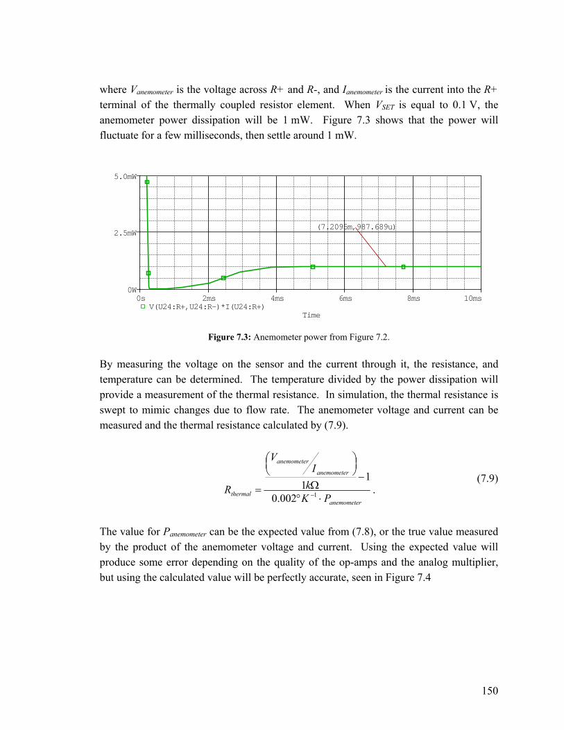
150
where Vanemometer is the voltage across R+ and R-, and Ianemometer is the current into the R+ terminal of the thermally coupled resistor element. When VSET is equal to 0.1 V, the anemometer power dissipation will be 1 mW. Figure 7.3 shows that the power will fluctuate for a few milliseconds, then settle around 1 mW.
Time
0s 2ms 4ms 6ms 8ms 10msV(U24:R+,U24:R-)*I(U24:R+)
0W
2.5mW
5.0mW
(7.2095m,987.689u)
Figure 7.3: Anemometer power from Figure 7.2.
By measuring the voltage on the sensor and the current through it, the resistance, and temperature can be determined. The temperature divided by the power dissipation will provide a measurement of the thermal resistance. In simulation, the thermal resistance is swept to mimic changes due to flow rate. The anemometer voltage and current can be measured and the thermal resistance calculated by (7.9).
anemometer
anemometer
anemometer
thermal PKk
IV
R⋅°
−Ω
⎟⎠⎞⎜
⎝⎛
= −1002.0
11 .
(7.9)
The value for Panemometer can be the expected value from (7.8), or the true value measured by the product of the anemometer voltage and current. Using the expected value will produce some error depending on the quality of the op-amps and the analog multiplier, but using the calculated value will be perfectly accurate, seen in Figure 7.4

151
R th
8.6K 8.8K 9.0K 9.2K 9.4K 9.6K 9.8K(((V(U24:R+,U24:R-)/I(U24:R+))/1000-1)/0.002)/(V(U24:R+,U24:R-)*I(U24:R+))
8K
9K
10K
Figure 7.4: Determination of thermal resistance from electrical measurements.
The thermal behavior of fabricated sensors can be characterized similarly to the method used in the ANSYS simulations in Chapter 4. The circuit in Figure 7.2, can be used to control the sensor to dissipate a constant amount of power. The electrical resistance can be determined by measuring the anemometer voltage and current. The power divided by the change in anemometer temperature yields the thermal conductance. After packaging, known flow rates can be pumped through the fluid channel, and the thermal conductance versus flow rate for the sensor can be determined. If the trend is fitted to King’s Law, the mathematical analysis in Chapter 3, and the formulation for thermal conductance versus sensor area, length-to-width ratio, and fluid velocity in Chapter 4, can be validated, or the equation for the Nusselt number refined. Because the sensors fabricated using the process presented in Chapter 5 required reworking that produced electrical connection between adjacent sensor bridges, the current applied to one bridge would also dissipate to the surrounding bridges. Since the bridges are not electrically isolated, accurate characterization would not be possible with the fabricated lot of wafers.

152
COALESCENCE OF RESULTS The discussion of various flow measurement methods in Chapter 1 has proven that the ideal method for sensing the flow rate in the implantable micropump system is via thermal flow sensing. This is founded on the fact that a thermal sensor:
• requires no moving parts • causes relatively small, if any, pressure drop • introduces no foreign particles into the fluid flow • can be made using biocompatible materials • can be integrated into the fluid channel with minimal assembly.
The comparison of different flow sensing methods in Chapter 2 suggests that the thermal anemometer is the most ideal and flexible solution. A calorimeter will waste an excessive amount of heat, which would be incompatible with the limited power source in an implantable system, and a time-of-flight sensor will require significant signal processing and control circuitry, taking up space. To optimize the performance of the anemometer, the design should aim to minimize the wasted power, by minimizing the thermal conductance from the heating element to the substrate. From (3.30), the sensitivity of can be maximized by increasing the thermal conductance to the fluid, and increasing the sensor overheat temperature. By adjusting the sensor geometry and calculating the effect on thermal conductance using MATLAB, it is discovered that the most efficient tradeoff of sensitivity and power consumption is obtained by the narrowest sensor that extends all the across the fluid channel. If a limit is placed on the overheat temperature, the sensitivity can be increased by increasing the sensor area, but at the expense of more power lost to the substrate.

153
The MATLAB analysis in Chapter 3 relies on the approximation of Nusselt number in (3.17), which is used to develop a form of King’s Law, where the thermal conductance to the fluid is a function of the square-root of the fluid velocity. Many representations of King’s Law fitted to experimental data show variation from this square-root dependence in different sensor designs. In order to more accurately predict the heat transfer to the flowing fluid, ANSYS simulations are performed in Chapter 4 to produce a form of King’s Law in which the fitting parameters are functions of the area and thermal length to width ratio. The constant-temperature control mode of thermal anemometers eliminates the effect of transient thermal properties on the sensor performance. In Chapter 6, three circuits are presented that will drive the sensor to a constant overheat temperature, and will also reduce the effect of ambient temperature fluctuations on sensor output.
I. OVERALL SENSITIVITY PREDICTION If the results from the mathematical analysis in Chapter 3 are combined with the expected sensor performance determined from the simulations in Chapter 6, the overall behavior of the sensor can be determined. From Figure 3.9, the thermal conductance is expected to vary from approximately 1020 erg/sec/°K at zero flow rate to 1150 erg/sec/°K at the maximum expected flow rate of 150 nL/min. The sensitivity of the circuits in Chapter 6 are characterized by the change in voltage versus change in thermal resistance, so the thermal resistance must be considered. When inverted and converted to units of W/°K, the thermal resistance at zero flow rate is approximately 9800 W/°K, and at maximum flow rate, the thermal resistance is approximately 8700 W/°K. In the middle of the range of flow rates (i.e. at U = 75 nL/min), the sensitivity of thermal resistance to fluid flow rate is calculated from the inverse of Figure 3.9 to be -5.1 W/°K/(nL/min). At the maximum flow rate, where the sensitivity should be the lowest, the sensitivity is calculated to be -3.4 W/°K/(nL/min). The sensitivities, quality factor for the default configuration, and the maximum quality factor of the circuits simulated in Chapter 6 are shown in Table 8.1.

154
Table 8.1 Sensitivities for Simulated Circuits in Chapter 6. Circuit
dVOUT/dRthermal
(µV/(W/°K)) dVOUT/dTAMB
(µV/°K) Quality Factor
(W) Max Quality Factor (W)
Basic (Figure 6.6) -93.5 -32.9 2.84 3.3 Transimpedance
(Figure 6.14) -45.8 -24.6 1.86 2.38
Stepped-down Leg (Figure 6.18)
-6.76 -31.8 0.212 1.0
The overall sensitivity, S, can be calculated by (8.1).
min/nL
thermal
thermal
OUToverall dU
dRdRdV
S = (8.1)
The typical overall sensitivity, calculated when the flow rate is equal to 75 nL/min, and the minimum overall sensitivity, calculated at the maximum flow rate, are shown in Table 8.2.
Table 8.2 Typical and Minimum Overall Sensitivities for Circuits in Chapter 6.
Circuit dVOUT/dRthermal
(µV/(W/°K)) Typical Soverall (µV/(nL/min))
Minimum Soverall (µV/(nL/min))
Basic (Figure 6.6)
-93.5 476.85 317.9
Transimpedance (Figure 6.14)
-45.8 233.58 155.72
Stepped-down Leg (Figure
6.18) -6.76 34.48 22.984
If the noise from the environment is characterized and quantified, a minimum realizable voltage may be determined. The sensitivity obtained from the circuit simulations is based on an overheat temperature of 10°K. If the minimum sensitivity turns out to be indistinguishable from noise, then the overheat temperature may be increased to improve the sensitivity, if the fluid will tolerate the small region of high temperature.
155
The other metric that may be calculated is the perceived change in flow rate with changes in ambient temperature. This may be calculated using (8.2), where M is the quality factor defined in Chapter 6.
AMB
OUT
thermal
OUT
nL
thermalAMB
nL
dTdV
dRdV
dUdRdT
dU 11
min/
min/ =
MdU
dRdTdU
nL
thermalAMB
nL 11
min/
min/ = (8.2)
Since it is the worst-case that is of interest, the minimum sensitivity is used for dRthermal/dUnL/min (-3.4 W/°K/(nL/min)). The resulting calculation for each circuit is shown in Table 8.3. The change in ambient temperature necessary to produce a 1 nL/min error in the measurement is also listed in Table 8.3, which is simply the inverse of dUnL/min/dTAMB. Table 8.3 Effect of Change in Ambient Temperature on Perceived Change in Flow Rate.
Circuit
Quality Factor (W) dUnL/min/dTAMB
(nL/min/°K) ΔTAMB for 1 nL/min
misread Basic (Figure
6.6) 2.84 -0.104 9.66
Transimpedance (Figure 6.14)
1.86 -0.158 6.32
Stepped-down Leg (Figure
6.18) 0.212 -1.39 0.721
By combining the expected thermal sensitivity from Chapter 3, with the sensitivity of the constant temperature control circuit in Chapter 6, the overall performance of the sensors can be evaluated. For the Wheatstone bridge with feedback amplifier and transimpedance circuit, the minimum sensitivity seen in Table 8.2 is 155 µV/(nL/min). Whether or not this is a sufficient value will depend on the level of noise in the system. However, if the flow rate is expected to change very slowly, the output of the constant-temperature circuit can be averaged to remove the noise, since it should be nearly a DC signal. If the output voltage at zero flow rate is known, or easily determined, a

156
differential amplifier can also be added as an output stage to increase the voltage change versus flow rate. The sensor used to determine the overall sensitivity has the nominal dimensions listed in Table 3.4, but the sensitivity may be increased if the sensor geometry is changed. According to the MATLAB and ANSYS analyses, the sensor geometry that produces the greatest sensitivity versus power consumed is as narrow as possible, stretching across the entire fluid channel. The risk in relying on this sensor geometry alone is that a very narrow and long sensor may be too fragile to fabricate. The process presented in Chapter 5 and the successful fabrication of sensors of various geometries shows that even the most narrow and long sensor is realizable. The MATLAB analysis in Chapter 3 suggests that a wider fluid channel will produce higher values of sensitivity, but the opposite is seen in the ANSYS simulations of Chapter 4. Competing effects influence the sensitivity when changing the width of the fluid channel. The wider channel allows for longer sensors, with greater area and thus greater thermal conductance to the fluid. At the same time, making the channel wider reduces the fluid velocity for a constant flow rate, reducing the sensitivity. The ANSYS simulation is likely to be most accurate, since the MATLAB model assumes a spreading resistance to an infinite body of fluid, and the assumptions made may not truly describe the scenario. Even though the ANSYS simulation is expected to be the most accurate, the relative changes in thermal conductance to the fluid between zero flow rate and with the maximum flow rate applied are much lower than expected.
II. FUTURE WORK To assess how well the ANSYS simulations translate to true behavior, fabricated sensors should be packaged and tested. The constant power circuit in Figure 7.2 can be used to characterize the actual circuits similar to the characterization done in ANSYS. For different flow rates, the sensor is driven to deliver a constant power, and the temperature is measured. The power divided by overheat temperature is equal to the thermal conductance. The thermal conductance trend can be fitted to King’s Law, and used as calibration for the sensor. The trend can also be used to refine the mathematical formulas used in MATLAB, or constraints in the ANSYS simulations. The major obstacle to overcome in order to progress with sensor characterization, model refinement, and circuit testing, is to successfully fabricate a usable set of sensors. The
157
successfully fabricated sensors presented in Chapter 5 are encapsulated polysilicon bridges situated above the KOH etched fluid channel that an electrical resistance can be measured across. However, because of reworking steps, electrical cross-connections between adjacent bridges are created. The issue requiring this rework has been resolved, but investigation into the removal of the residue following the boron doping should be done before committing more wafers to entire fabrication process. Once sensors are successfully fabricated, packaging and characterization can be done, described in Chapter 7, and the results can be used to refine the models in Chapters 3 and 4. As seen in Figure 6.12 and Figure 6.15, there is usually a large DC offset to the voltage signal dependent on flow rate. At zero flow rate the voltage is near 2 Volts, and only changes by a few tens of millivolt over the range of flow rates. If a complementary circuit could sample and hold this DC offset, then a differential amplifier could be used to amplify the change in voltage due to flowing fluid. This would allow the output to vary across the entire range of available voltage. When combined with the proposed sensor geometry, constructed using the fabrication process presented, and incorporated into the designed constant-temperature control circuit, a flow sensor with maximum sensitivity and optimum performance will be produced.

158
APPENDIX A: MATLAB SCRIPTS FOR CHAPTER 3
matl_props.m %using to define material constants used in calculations k_Si=13000000; %erg/sec/cm/deg_C k_SiN=3010000; %erg/sec/cm/deg_C k_H2O=58000; %erg/sec/cm/deg_C cp_H2O=41870000; %erg/g/deg_C cp_Si=7000000; %erg/g/deg_C cp_SiN=7106000; %erg/g/deg_C d_Si=2.33; %g/cm^3 d_SiN=3.184; %g/cm^3 d_H2O=0.998; %g/cm^3 visc_H2O=0.01; %g/cm^3 res_Si=0.0048; %ohm-cm t_e=0.00006; %cm t_t=0.00009; %cm
calculations.m %calculations used during variable sweep analysis run('matl_props'); %electrical: r_attach=(res_Si/2/t_e)*log(1+CW/W_e-L_e/W_e); r_heater=res_Si*L_e/W_e/t_e; r_elect_total=2*r_attach+r_heater; %thermal: k_comp=(t_e*k_Si+(t_t-t_e)*k_SiN)/t_t; %zeta=max([L_t/W_t W_t/L_t]); zeta=L_t/W_t; r_substr=L_t/(2*k_comp*W_t*t_t)+1/(2*k_comp*t_t)*log(1+CW/W_t-L_t/W_t); r_convec0=(1.614-.226*log(zeta))/(k_H2O*pi*sqrt(L_t*W_t)); %area = W_t*L_t;
159
%g_convec0 = k_H2O*pi*(area^0.5)/((zeta^0.5)*(asinh(1/zeta)+(1/zeta)*asinh(zeta)+(zeta/3)*(1+(1/(zeta^3))-(1+(1/(zeta^2)))^(3/2)))); %r_convec0=1/g_convec0; Re_num=d_H2O*u_cmps*CW/visc_H2O; Pr_num=cp_H2O*visc_H2O/k_H2O; Nu_num=0.664*Pr_num^(1/3)*Re_num^(1/2); r_convec=r_convec0/(1+Nu_num); r_therm_total=1/(2/r_convec+2/r_substr); q_ergps=T_overheat/r_therm_total; q_watt=q_ergps/10000000; current=sqrt(q_watt/r_heater); voltage=current*r_elect_total;
variable_sweep.m – plotting commands are excluded for conciseness %the following program sweeps various physical parameters of the sensor and %generates plots of the results close all hidden clear all %%%%%%%%%%%%%%%%%%%%%%%%%%%%%%%%%%%%%%%%%%%%%%%%%%%%%%%%%%%%%%%%%%%%%%%%%%%%%% %calculates thermal resistance vs. flow rate CW=.01; T_overheat=10; W_e=.0002; W_t=.0008; L_e=.005; L_t=.005; for i=1:151 u_nLpm(i)=(i-1); u_cmps=(i-1) / 60 / (pi*(CW/2)^2) / 1000000; run('calculations'); convection_conductanceu(i)=2/r_convec; conduction_conductanceu(i)=2/r_substr; total_conductanceu(i)=1/r_therm_total; convec_percentu(i)=convection_conductanceu(i)/total_conductanceu(i)*100; power_ergpsu(i)=q_ergps; power_mwattu(i)=q_watt*1000; voltageu(i)=voltage; end clear CW T_overheat W_e L_e W_t L_t A Z; %%%%%%%%%%%%%%%%%%%%%%%%%%%%%%%%%%%%%%%%%%%%%%%%%%%%%%%%%%%%%%%%%%%%%% %calculates thermal resistance vs L:W ratio CW=.01; T_overheat=10; W_e=.0002; L_e=.005; A=.0008*.005; Z=1:.5:25; u_cmps=75 / 60 / (pi*(CW/2)^2) / 1000000; for i=1:size(Z,2) W_t=sqrt(A/Z(i)); L_t=sqrt(A*Z(i)); run('calculations'); convection_conductanceZ(i)=2/r_convec; conduction_conductanceZ(i)=2/r_substr;

160
total_conductanceZ(i)=1/r_therm_total; convec_percentZ(i)=convection_conductanceZ(i)/total_conductanceZ(i)*100; end clear CW T_overheat W_e L_e W_t L_t A Z; %%%%%%%%%%%%%%%%%%%%%%%%%%%%%%%%%%%%%%%%%%%%%%%%%%%%%%%%%%%%%%%%% %calculates thermal resistance vs heater area CW=.01; T_overheat=10; W_e=.0002; L_e=.005; u_cmps=75 / 60 / (pi*(CW/2)^2) / 1000000; Z=50/8; A=.0000001:.0000001:.00001600; for i=1:size(A,2) W_t=sqrt(A(i)/Z); L_t=sqrt(A(i)*Z); run('calculations'); convection_conductanceA(i)=2/r_convec; conduction_conductanceA(i)=2/r_substr; total_conductanceA(i)=1/r_therm_total; convec_percentA(i)=convection_conductanceA(i)/total_conductanceA(i)*100; end clear CW T_overheat W_e L_e W_t L_t A Z; %%%%%%%%%%%%%%%%%%%%%%%%%%%%%%%%%%%%%%%%%%%%%%%%%%%%%%%%%%%%%%%%%%%%%%%% %sweeps channel width %thermal length is equal to channel width T_overheat=10; W_e=.0002; W_t=.0008; u_nLpm=75; chan_wid=0.0010:0.0001:.0100; for i=1:size(chan_wid,2) CW=chan_wid(i); L_t=chan_wid(i); L_e=chan_wid(i); u_cmps=u_nLpm / 60 / (pi*(CW/2)^2) / 1000000; run('calculations'); convection_conductancecw(i)=2/r_convec; conduction_conductancecw(i)=2/r_substr; total_conductancecw(i)=1/r_therm_total; convec_percentcw(i)=convection_conductancecw(i)/total_conductancecw(i)*100; power_ergpscw(i)=q_ergps; power_mwattcw(i)=q_watt*1000; voltagecw(i)=voltage; end clear CW T_overheat W_e L_e W_t L_t A Z; %%%%%%%%%%%%%%%%%%%%%%%%%%%%%%%%%%%%%%%%%%%%%%%%%%%%%%%%%%%%%%%%%%%%%%%% %sweeps heater thermal width %lengths are equal to channel width T_overheat=10; CW=.01; L_t=.005; L_e=.005; W=.0004:.0002:.01; W_e=0.0002; u_nLpm=75; u_cmps=u_nLpm / 60 / (pi*(CW/2)^2) / 1000000;

161
for i=1:size(W,2) W_t=W(i); run('calculations'); convection_conductancew(i)=2/r_convec; conduction_conductancew(i)=2/r_substr; total_conductancew(i)=1/r_therm_total; convec_percentw(i)=convection_conductancew(i)/total_conductancew(i)*100; power_ergpsw(i)=q_ergps; power_mwattw(i)=q_watt*1000; voltagew(i)=voltage; end clear CW T_overheat W_e L_e W_t L_t A Z; %%%%%%%%%%%%%%%%%%%%%%%%%%%%%%%%%%%%%%%%%%%%%%%%%%%%%%%%%%%%%%%%%%%%%%%%%%%%%% %calculates thermal resistance vs. flow rate CW=.01; T=0:50; W_e=.0002; L_e=.005; L_t=.005; W_t=.0008; u_cmps=75 / 60 / (pi*(CW/2)^2) / 1000000; for i=1:size(T,2) T_overheat=T(i); run('calculations'); convection_conductancet(i)=2/r_convec; conduction_conductancet(i)=2/r_substr; total_conductancet(i)=1/r_therm_total; convec_percentt(i)=convection_conductancet(i)/total_conductancet(i)*100; power_ergpst(i)=q_ergps; power_mwattt(i)=q_watt*1000; voltaget(i)=voltage; end clear CW T_overheat W_e L_e W_t L_t A Z;

162
APPENDIX B: MATLAB SCRIPTS FOR CHAPTER 4
therm_res_script_creator.m %this code will create the ANSYS script files used to perform thermal %spreading resistance simulations % %The fluid bulk has a temperature of 310 degrees Kelvin, and the heating %element generates 10000 erg/s (1 mW) of thermal power. The temperature of %the heating element is exported to a text file analyzed by a MATLAB %program. Six flow rates from 0 to the max flow are used in the %simulation. max_flow_speed=0.30; %cm/sec run_file = fopen('C:\GRAD_RESEARCH\matlab_and_simulink\scripts\therm_res\runall.txt','w'); Z=[.04 .08 .125 .25 .5 1 2 4 8 12.5 25]; %values of thermal length to width ratio used A=[25 100 225 400 625 900 1225 1600 2025]; %values of heater area (square um used) flow_speed=zeros(5); for k=1:1:size(Z,2) for j=1:1:size(A,2) area=A(j); ratio=Z(k); %Calculate width and length - since Z=W/L and A=W*L, W=sqrt(A*Z). %Then convert length and width from um to cm W=sqrt(area*ratio); L=area/W; W_cm=W/10000; L_cm=L/10000; %Set up the file name and path for the script file ansys_fl_nm=strcat('T_res-sim_a',num2str(area),'z',num2str(ratio)); file_path='C:\GRAD_RESEARCH\matlab_and_simulink\scripts\therm_res\'; ansys_scr=fopen(strcat(file_path,ansys_fl_nm,'.txt'),'w'); %Build the heater and 'infinite' fluid - a rectangular prism %1*1.1*1.2 mm's - not having a perfect cube for the structure %prevents mesh symmetry which may distort results unfavorably for

163
%square (Z=1) heaters fprintf(ansys_scr,'FINISH \r\n'); fprintf(ansys_scr,'/CLEAR,START \r\n'); fprintf(ansys_scr,'/FILNAM,%s,0 \r\n',ansys_fl_nm); fprintf(ansys_scr,'/PREP7 \r\n'); fprintf(ansys_scr,'BLC5,0,0,.1,.12,.1 \r\n'); fprintf(ansys_scr,'BLC5,0,0,%s,%s,-.001 \r\n',W_cm, L_cm); fprintf(ansys_scr,'VDELE,ALL \r\n'); fprintf(ansys_scr,'ASBA,1,8,,DELE,KEEP \r\n'); fprintf(ansys_scr,'VA,2,3,4,5,6,8,13 \r\n'); fprintf(ansys_scr,'VA,7,8,9,10,11,12 \r\n'); fprintf(ansys_scr,'VGLUE,1,2 \r\n'); %Set up the element type and material properties of the heater and %the fluid. fprintf(ansys_scr,'ET,1,FLUID142 \r\n'); fprintf(ansys_scr,'/mplib,READ,''C:\\GRAD_RESEARCH\\ansys\\matl_lib'' \r\n'); fprintf(ansys_scr,'MAT,1 \r\n'); fprintf(ansys_scr,'mpread,''water'',CGS_MPL,,LIB \r\n'); fprintf(ansys_scr,'MAT,2 \r\n'); fprintf(ansys_scr,'mpread,''ideal'',CGS_MPL,,LIB \r\n'); fprintf(ansys_scr,'VSEL,S,VOLU,,1,1,1 \r\n'); fprintf(ansys_scr,'VATT,1,-1,1,-1 \r\n'); fprintf(ansys_scr,'ALLSEL \r\n'); fprintf(ansys_scr,'VSEL,S,VOLU,,2,2,1 \r\n'); fprintf(ansys_scr,'VATT,2,-1,1,-1 \r\n'); fprintf(ansys_scr,'ALLSEL \r\n'); %ANSYS has a smart size feature which will automatically size lines %so that smaller features have a finer mesh and larger features are %coarser. fprintf(ansys_scr,'MSHKEY,0 \r\n'); fprintf(ansys_scr,'MSHAPE,1 \r\n'); fprintf(ansys_scr,'ALLSEL \r\n'); fprintf(ansys_scr,'SMRTSIZE,1 \r\n'); fprintf(ansys_scr,'ALLSEL \r\n'); fprintf(ansys_scr,'VMESH,ALL \r\n'); %Set options for the FLOTRAN simulation - e.g. simulation %iterations, termination criteria, reference conditions, fprintf(ansys_scr,'FLDATA1,SOLU,TEMP,T \r\n'); fprintf(ansys_scr,'FLDATA1,ITER,EXEC,150 \r\n'); fprintf(ansys_scr,'FLDATA3,TERM,PRES,0.001 \r\n'); fprintf(ansys_scr,'FLDATA3,TERM,TEMP,0.00000001 \r\n'); fprintf(ansys_scr,'FLDATA3,TERM,VX,0.001 \r\n'); fprintf(ansys_scr,'FLDATA3,TERM,VY,0.001 \r\n'); fprintf(ansys_scr,'FLDATA3,TERM,VZ,0.001 \r\n'); fprintf(ansys_scr,'FLDATA7,PROT,DENS,CONSTANT \r\n'); fprintf(ansys_scr,'FLDATA7,PROT,VISC,CONSTANT \r\n'); fprintf(ansys_scr,'FLDATA7,PROT,COND,CONSTANT \r\n'); fprintf(ansys_scr,'FLDATA7,PROT,SPHT,CONSTANT \r\n'); fprintf(ansys_scr,'FLDATA8,NOMI,DENS,0.997 \r\n'); %density setting fprintf(ansys_scr,'FLDATA8,NOMI,VISC,0.01 \r\n'); %viscosity setting fprintf(ansys_scr,'FLDATA8,NOMI,COND,58000 \r\n'); %thermal cond setting fprintf(ansys_scr,'FLDATA8,NOMI,SPHT,41810000 \r\n'); %specific heat setting fprintf(ansys_scr,'FLDATA14,TEMP,BULK,310 \r\n'); fprintf(ansys_scr,'FLDATA14,TEMP,TTOT,310 \r\n'); fprintf(ansys_scr,'FLDATA14,TEMP,NOMI,310 \r\n'); fprintf(ansys_scr,'FLDATA15,PRES,REFE,1013250 \r\n'); fprintf(ansys_scr,'FLDATA22,MAXI,TEMP,1500 \r\n'); fprintf(ansys_scr,'FLDATA21,CONV,TEMP,1e-12 \r\n'); fprintf(ansys_scr,'FLDATA23,DELT,TEMP,1e-12 \r\n'); %Set boundary conditions and loads: %Zero pressure at outlet - area 4 fprintf(ansys_scr,'ASEL,S,,,4,4,1 \r\n'); fprintf(ansys_scr,'DA,ALL,PRES,0,1 \r\n');
164
%No fluid leaving (zero velocity) the infinite fluid except at the outlet fprintf(ansys_scr,'ASEL,S,,,5,6,1 \r\n'); fprintf(ansys_scr,'DA,ALL,VX,0,1 \r\n'); fprintf(ansys_scr,'ASEL,S,,,2,2,1 \r\n'); fprintf(ansys_scr,'DA,ALL,VZ,0,1 \r\n'); fprintf(ansys_scr,'ASEL,S,,,13,13,1 \r\n'); fprintf(ansys_scr,'DA,ALL,VZ,0,1 \r\n'); %No slip condition on the part of the heating element contacting %the fluid. fprintf(ansys_scr,'ASEL,S,,,8,8,1 \r\n'); fprintf(ansys_scr,'DA,ALL,VX,0,1 \r\n'); fprintf(ansys_scr,'DA,ALL,VY,0,1 \r\n'); fprintf(ansys_scr,'DA,ALL,VZ,0,1 \r\n'); %Fluid temperature is 310 on the area opposite the heating element fprintf(ansys_scr,'ASEL,S,,,2,2,1 \r\n'); fprintf(ansys_scr,'DA,ALL,TEMP,310,1 \r\n'); %Set inlet and outlet fluid velocity - for the first simulation, %these are zero fprintf(ansys_scr,'ASEL,S,,,4,4,1 \r\n'); fprintf(ansys_scr,'DA,ALL,VY,%10.8f,1 \r\n',0); fprintf(ansys_scr,'ASEL,S,,,3,3,1 \r\n'); fprintf(ansys_scr,'DA,ALL,VY,%10.8f,1 \r\n',0); fprintf(ansys_scr,'ALLSEL \r\n'); %Set heat generation of 10000 erg/s on heating element fprintf(ansys_scr,'BFV,2,HGEN,%10.8f \r\n',10000/(L_cm*W_cm*.001)); fprintf(ansys_scr,'ALLSEL \r\n'); %Apply initial temperature of 310 in all elements fprintf(ansys_scr,'IC,ALL,TEMP,310 \r\n'); fprintf(ansys_scr,'/SOLU \r\n'); fprintf(ansys_scr,'SOLVE \r\n'); %Export temperature of nodes on heater to txt file fprintf(ansys_scr,'/POST1 \r\n'); fprintf(ansys_scr,'SET,LAST \r\n'); fprintf(ansys_scr,'VSEL,S,VOLU,,2,2,1,1 \r\n'); fprintf(ansys_scr,'/FORMAT,,F,10 \r\n'); fprintf(ansys_scr,'/HEADER,OFF,OFF,OFF,OFF,OFF,OFF \r\n'); txt_fl_nm=strcat('T_res-sim_a',num2str(area),'z',num2str(ratio),'fs0'); fprintf(ansys_scr,'/OUTPUT,C:\\GRAD_RESEARCH\\ansys\\results\\%s,txt,,APPEND \r\n',strcat(txt_fl_nm,'_results')); fprintf(ansys_scr,'PRNSOL,TEMP \r\n'); fprintf(ansys_scr,'/OUTPUT,TERM \r\n'); %Repeat the simulation for flowing fluid for i=1:1:5 flow_speed(i)=(i)*max_flow_speed/5; fprintf(ansys_scr,'ALLSEL \r\n'); fprintf(ansys_scr,'/PREP7 \r\n'); fprintf(ansys_scr,'ASEL,S,,,5,6,1 \r\n'); fprintf(ansys_scr,'DADELE,ALL,VX \r\n'); fprintf(ansys_scr,'DA,ALL,VX,0,1 \r\n'); fprintf(ansys_scr,'ASEL,S,,,2,2,1 \r\n'); fprintf(ansys_scr,'DADELE,ALL,VZ \r\n'); fprintf(ansys_scr,'DA,ALL,VZ,0,1 \r\n'); fprintf(ansys_scr,'ASEL,S,,,13,13,1 \r\n'); fprintf(ansys_scr,'DADELE,ALL,VZ \r\n'); fprintf(ansys_scr,'DA,ALL,VZ,0,1 \r\n'); fprintf(ansys_scr,'ASEL,S,,,8,8,1 \r\n'); fprintf(ansys_scr,'DADELE,ALL,VX \r\n'); fprintf(ansys_scr,'DADELE,ALL,VY \r\n'); fprintf(ansys_scr,'DADELE,ALL,VZ \r\n'); fprintf(ansys_scr,'DA,ALL,VX,0,1 \r\n'); fprintf(ansys_scr,'DA,ALL,VY,0,1 \r\n');
165
fprintf(ansys_scr,'DA,ALL,VZ,0,1 \r\n'); %Instead of zero the fluid velocity will be applied at the %inlet and outlet fprintf(ansys_scr,'ASEL,S,,,4,4,1 \r\n'); fprintf(ansys_scr,'DADELE,ALL,VY \r\n'); fprintf(ansys_scr,'DA,ALL,VY,%10.8f,1 \r\n',flow_speed(i)); fprintf(ansys_scr,'ASEL,S,,,3,3,1 \r\n'); fprintf(ansys_scr,'DADELE,ALL,VY \r\n'); fprintf(ansys_scr,'DA,ALL,VY,%10.8f,1 \r\n',flow_speed(i)); fprintf(ansys_scr,'ALLSEL \r\n'); fprintf(ansys_scr,'/SOLU \r\n'); fprintf(ansys_scr,'SOLVE \r\n'); %Export temperature of nodes on heater to txt file fprintf(ansys_scr,'/POST1 \r\n'); fprintf(ansys_scr,'SET,LAST \r\n'); fprintf(ansys_scr,'VSEL,S,VOLU,,2,2,1,1 \r\n'); fprintf(ansys_scr,'/HEADER,OFF,OFF,OFF,OFF,OFF,OFF \r\n'); txt_fl_nm=strcat('T_res-sim_a' ,num2str(area),'z',num2str(ratio),'fs',num2str(i)); fprintf(ansys_scr,'/OUTPUT,C:\\GRAD_RESEARCH\\ansys\\results\\%s,txt,,APPEND \r\n',strcat(txt_fl_nm,'_results')); fprintf(ansys_scr,'PRNSOL,TEMP \r\n'); fprintf(ansys_scr,'/OUTPUT,TERM \r\n'); end fclose(ansys_scr); fprintf(run_file,'%s \r\n',strcat('/INPUT,',file_path,ansys_fl_nm,',txt')); end end fclose(run_file);
TR_control_script.m %%the following code runs each individual scripts used to read the data %%produced from the thermal resistance equations, fit the data, and plot it close all; TR_set_consts; %sets up arrays and constants TR_read_files; %reads results of simulation files to h_cond_f thermal conductance matrix TR_fit_h; %fits h_cond_f matrix to spread_cond_func function TR_fill_ideal_h; %fills matrix h_ideal with values calculated from results of TR_fit_h TR_fit_kings_law; %fits each A-Z set in h_cond_f to King's Law trend TR_display_h_vs_flow; %allows user to select area and ratio to display data and fitted trend vs. flow velocity
TR_set_consts.m amb_temp=310; %deg_K power_gen=10000; %erg/sec max_flow = 0.3; %cm/sec Zx=[.04 .08 .125 .25 .5 1 2 4 8 12.5 25]; %thermal length to width ratio Zxlog=log(Zx); %log of Zx Ax=[0 25 100 225 400 625 900 1225 1600 2025]; %square um [Am,Zm]=meshgrid(Ax,Zxlog); Amt=Ax(2:size(Ax,2)); Zmt=Zxlog; [Amtmg, Zmtmg] = meshgrid(Amt,Zmt);
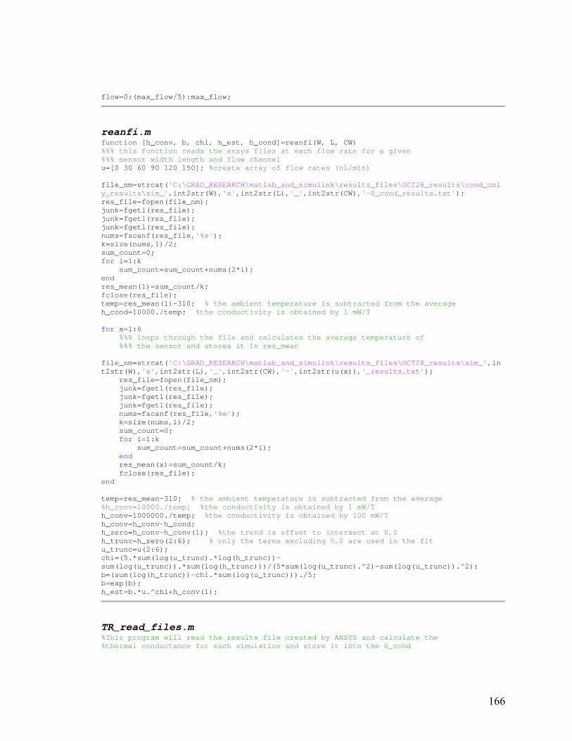
166
flow=0:(max_flow/5):max_flow;
reanfi.m function [h_conv, b, chi, h_est, h_cond]=reanfi(W, L, CW) %%% this function reads the ansys files at each flow rate for a given %%% sensor width length and flow channel u=[0 30 60 90 120 150]; %create array of flow rates (nL/min) file_nm=strcat('C:\GRAD_RESEARCH\matlab_and_simulink\results_files\OCT28_results\cond_only_results\sim_',int2str(W),'x',int2str(L),'_',int2str(CW),'-0_cond_results.txt'); res_file=fopen(file_nm); junk=fgetl(res_file); junk=fgetl(res_file); junk=fgetl(res_file); nums=fscanf(res_file,'%e'); k=size(nums,1)/2; sum_count=0; for i=1:k sum_count=sum_count+nums(2*i); end res_mean(1)=sum_count/k; fclose(res_file); temp=res_mean(1)-310; % the ambient temperature is subtracted from the average h_cond=10000./temp; %the conductivity is obtained by 1 mW/T for x=1:6 %%% loops through the file and calculates the average temperature of %%% the sensor and stores it in res_mean file_nm=strcat('C:\GRAD_RESEARCH\matlab_and_simulink\results_files\OCT28_results\sim_',int2str(W),'x',int2str(L),'_',int2str(CW),'-',int2str(u(x)),'_results.txt'); res_file=fopen(file_nm); junk=fgetl(res_file); junk=fgetl(res_file); junk=fgetl(res_file); nums=fscanf(res_file,'%e'); k=size(nums,1)/2; sum_count=0; for i=1:k sum_count=sum_count+nums(2*i); end res_mean(x)=sum_count/k; fclose(res_file); end temp=res_mean-310; % the ambient temperature is subtracted from the average %h_conv=10000./temp; %the conductivity is obtained by 1 mW/T h_conv=1000000./temp; %the conductivity is obtained by 100 mW/T h_conv=h_conv-h_cond; h_zero=h_conv-h_conv(1); %the trend is offset to intersect at 0,0 h_trunc=h_zero(2:6); % only the terms excluding 0,0 are used in the fit u_trunc=u(2:6); chi=(5.*sum(log(u_trunc).*log(h_trunc))-sum(log(u_trunc)).*sum(log(h_trunc)))/(5*sum(log(u_trunc).^2)-sum(log(u_trunc)).^2); b=(sum(log(h_trunc))-chi.*sum(log(u_trunc)))./5; b=exp(b); h_est=b.*u.^chi+h_conv(1);
TR_read_files.m %This program will read the results file created by ANSYS and calculate the %thermal conductance for each simulation and store it into the h_cond

167
%matrix %Either one file can be read, or if multiple simulations are run the %average of them can be determined file_folder='SEP05_noslip_results'; %for one set %file_folder=['JUN19_results1'; 'JUN19_results2'; 'JUN19_results3';'JUN19_results4'; 'JUN19_results5'; 'JUN19_results6']; %num_files=6; %for multiple sets only for f=1:1:6 h_cond=zeros(size(Zx,2),size(Ax,2)); %for file=1:1:num_files %for multiple sets only for i=1:1:size(Ax,2) for j=1:1:size(Zx,2) if(Ax(i)==0) h_cond(j,i)=0; else A=Ax(i); Z=Zx(j); file_nm=strcat('C:\GRAD_RESEARCH\matlab_and_simulink\results_files\', file_folder,'\T_res-sim_a',int2str(A),'z',num2str(Z),'fs',int2str(f-1),'_results.txt'); %file_nm=strcat('C:\GRAD_RESEARCH\matlab_and_simulink\results_files\', file_folder(file,:),'\T_res-sim_a',int2str(A),'z',num2str(Z),'fs',int2str(f-1),'_results.txt'); res_file=fopen(file_nm); junk=fgetl(res_file); junk=fgetl(res_file); junk=fgetl(res_file); nums=fscanf(res_file,'%e'); k=size(nums,1)/2; sum_count=0; for a=1:k sum_count=sum_count+nums(2*a); end res_mean=sum_count/k; %the following lines must be consistent with the simulation %setup, where 310 (deg_K) is the ambient temperature and 10000 (erg/sec) is %the power generated by the heater temp=res_mean-amb_temp; % the ambient temperature is subtracted from the average h_cond(j,i)=h_cond(j,i)+power_gen./temp; %the conductance is obtained by 10000 erg/s/Temp fclose(res_file); end end end %end %for multiple sets only % h_cond=h_cond./num_files; %for multiple sets only h_cond_f(:,:,f)=h_cond(:,:); end clear h_cond i j k file_folder file_nm res_file junk nums sum_count temp a f res_mean A Z;
TR_fit_h.m %This program obtains the parameters for the spreading conductance function %based on the data read into the h_cond matrix. The R^2 error is %calculated to indicate how well the curve fits to the data.

168
c0=[.002 0 -0.065 0.01 1.2 0.5]; options = optimset('lsqcurvefit'); options.MaxFunEvals = 5000; lower=[.001 -.001 -.08 -.01 0.5 0.3]; upper=[.003 .001 -.04 .05 2 1]; for f=1:1:size(flow,2) m=0; for i=1:1:size(Ax,2) for j=1:1:size(Zx,2) m=m+1; Al(m)=Ax(i); Zl(m)=Zx(j); hl(m)=h_cond_f(j,i,f); end end AZs=[Al(1,:) ; Zl(1,:)]; [c(:,f), resnorm(f)]=lsqcurvefit(@spread_cond_func, c0, AZs, hl, lower, upper, options); var(:,:)=(h_cond_f(:,:,f)- mean2(h_cond_f(:,:,f)) * ones(size(h_cond_f,1),size(h_cond_f,2)) ); r_error(f)=1-(resnorm(f)/(sum(sum( var .^2 )))'); end clear m f var resnorm c0 lower upper Al Zl hl AZs;
TR_fill_ideal.m %This program generates a matrix of thermal conductances based on the fitting parameters obtained in TR_fit_h. h_cond_ideal=zeros(size(Zx,2),size(Ax,2),size(flow,2)); for f=1:1:size(flow,2) for i=1:1:size(Ax,2) for j=1:1:size(Zx,2) AZ=[Ax(i); Zx(j)]; h_cond_ideal(j,i,f)=spread_cond_func(c(:,f), AZ); end end end clear f i j AZ;
TR_fit_kings_law.m %This program fits the King's Law function of thermal conductance vs. flow %for each set of area and ratio data. The King's law coefficient and %exponent are stored in kl_params_a. %h_idealt(:,:,:)=h_ideal(:,3:size(h_ideal,2),:); h_condt(:,:,:)=h_cond_f(:,2:size(h_cond_f,2),:); a0=[.01 .85]; options = optimset('lsqcurvefit'); options.MaxFunEvals = 5000; lower=[.001 .7]; upper=[1 1]; m=0; for i=1:1:(size(Amt,2)) for j=1:1:size(Zmt,2)

169
for f=1:1:size(flow,2) %hx_i(f)=h_ideal(j,i,f); hx_a(f)=h_condt(j,i,f); end %hx_i=hx_i./hx_i(1); %[a_i, resnorm_i]=lsqcurvefit(@kings_law_func, a0, flow, hx_i, lower, upper, options); %kl_params_i(j,ii,:)=a_i; hx_a=hx_a./hx_a(1); [a_a, resnorm_a]=lsqcurvefit(@kings_law_func, a0, flow, hx_a, lower, upper, options); kl_params_a(j,i,:)=a_a; coeff_norm(j,i)=kl_params_a(j,i,1)/sqrt(Amt(i)); m=m+1; Al(m)=Amt(i); Zl_log(m)=Zmt(j); kl_coeffl(m)=kl_params_a(j,i,1); end end AZs=[Al(1,:) ; Zl_log(1,:)]; c_kl0 = [0 0 -0.0011 -0.001 0.02 0.4]; lower=[-.001 -.001 -.02 -.01 0.01 0.3]; upper=[.001 .001 0 0 0.03 0.6]; [c_kl, resnorm_kl]=lsqcurvefit(@king_law_coeff_func, c_kl0, AZs, kl_coeffl, lower, upper, options); var_kl=(kl_params_a(:,:,1)- mean2(kl_params_a(:,:,1)) * ones(size(kl_params_a,1),size(kl_params_a,2)) ); r_error_kl=1-(resnorm_kl/(sum(sum( var_kl .^2 )))'); clear hx_a a0 lower upper a_a resnorm_a i j f;
TR_display_h_vs_flow.m %This program is used to display the thermal conductance vs. flow velocity %for any desired area and ratio. Both the simulation results and fitted %King's Law trend are plotted. area_index=size(Amt,2); ratio_index=size(Zmt,2); while(area_index~=0) close all for f=1:1:6 h_f(f)=h_condt(ratio_index,area_index,f); h_f_fit(f)=h_condt(ratio_index,area_index,1)*kings_law_func(kl_params_a(ratio_index,area_index,:),flow(f)); end plot (flow, h_f,flow,h_f_fit); xlabel('Flow Velocity (cm/s)'); ylabel('Thermal Conductance (cgs units)'); title(strcat('h vs. flow for Area = ',... num2str(Amt(area_index)),... 'cm^2 and Ratio (log) = ',... num2str(Zmt(ratio_index))),... strcat( 'King''s Law Fit: h = '... ,num2str(h_condt(ratio_index,area_index,1)),... '*(1+',... num2str(kl_params_a(ratio_index,area_index,1)),...

170
'*u^',... num2str(kl_params_a(ratio_index,area_index,2)),... ')')); disp(' ') area_index=input('Enter Area Index: '); ratio_index=input('Enter Ratio Index: '); end close all; clear area_index ratio_index h_f h_f_fit;
script_creator.m %%the following program creates the sensor model using Rhino CAD software, %%and the script file read by ANSYS to perform the simulation for 6 %%different flow rates write_rhino=1; write_ansys=1; %CW = 100 Ws_um=[4 8 20 4 4 20 20]; Ls_um=[98 98 98 50 20 20 40]; CWs_um=[100 100 100 100 100 100 100]; %CW = 60 % Ws_um=[4 8 12 4 4 12 12]; % Ls_um=[58 58 58 30 20 20 40]; % CWs_um=[60 60 60 60 60 60 60]; %%CW = 32 % Ws_um=[4 8 16 4 4 8 16]; % Ls_um=[30 30 30 16 8 16 16]; % CWs_um=[32 32 32 32 32 32 32]; for i=1:size(Ws_um,2) W_um=Ws_um(i); L_um=Ls_um(i); CW_um=CWs_um(i); %Re_num=150*10^-6/(pi*((CW_um/10000)/2)^2*60)*.997*(CW_um/10000)/.01; %CL_um=ceil((1000*Re_num*0.06)*CW_um); CL_um=200; poly_t_um=0.9; overlap_um=5; rhino_fl_nm=strcat('model_',num2str(W_um),'x',num2str(L_um),'_',num2str(CW_um)); rhino_fl_path=strcat('C:\GRAD_RESEARCH\rhino\'); %convert to cm CW=CW_um/10000; CL=CL_um/10000; W=W_um/10000; L=L_um/10000; poly_t=poly_t_um/10000; overlap=overlap_um/10000; if(write_rhino==1) rhino_scr=fopen(strcat('C:\GRAD_RESEARCH\matlab_and_simulink\scripts\',rhino_fl_nm,'.txt'),'w'); fprintf(rhino_scr,'-DocumentProperties u a 0.000001 _enter _enter\r\n'); %fprintf(rhino_scr,'-layer n poly r poly 255,0,0 c poly _enter\r\n'); fprintf(rhino_scr,'top \r\n'); fprintf(rhino_scr,'polyline ');

171
fprintf(rhino_scr,'%010.8f,%010.8f ',L/2,W/2); fprintf(rhino_scr,'%010.8f,%010.8f ',CW/2+overlap,(CW-L)/2+W/2+overlap); fprintf(rhino_scr,'%010.8f,%010.8f ',CW/2+overlap,-(CW-L)/2-W/2-overlap); fprintf(rhino_scr,'%010.8f,%010.8f ',L/2,-W/2); fprintf(rhino_scr,'close\r\n'); fprintf(rhino_scr,'extrude all _enter b=no c=yes e=yes %010.8f \r\n', poly_t/2); fprintf(rhino_scr,'rotate3d all _enter 0,0,0 1,0,0 -90 _enter \r\n'); fprintf(rhino_scr,'all \r\n'); fprintf(rhino_scr,'-ExportWithOrigin _enter '); fprintf(rhino_scr, '%s',strcat('"',rhino_fl_path, rhino_fl_nm,'_1','.sat','"')); fprintf(rhino_scr,' _enter\r\n'); fprintf(rhino_scr,'delete\r\n'); fprintf(rhino_scr,'polyline '); fprintf(rhino_scr,'%010.8f,%010.8f ',L/2,-W/2); fprintf(rhino_scr,'%010.8f,%010.8f ',-L/2,-W/2); fprintf(rhino_scr,'%010.8f,%010.8f ',-L/2,W/2); fprintf(rhino_scr,'%010.8f,%010.8f ',L/2,W/2); fprintf(rhino_scr,'close\r\n'); fprintf(rhino_scr,'extrude all _enter b=no c=yes e=yes %010.8f \r\n', poly_t/2); fprintf(rhino_scr,'rotate3d all _enter 0,0,0 1,0,0 -90 _enter \r\n'); fprintf(rhino_scr,'all \r\n'); fprintf(rhino_scr,'-ExportWithOrigin _enter '); fprintf(rhino_scr, '%s',strcat('"',rhino_fl_path, rhino_fl_nm,'_2','.sat','"')); fprintf(rhino_scr,' _enter\r\n'); fprintf(rhino_scr,'delete\r\n'); fprintf(rhino_scr,'polyline '); fprintf(rhino_scr,'%010.8f,%010.8f ',-L/2,-W/2); fprintf(rhino_scr,'%010.8f,%010.8f ',-CW/2-overlap,-(CW-L)/2-W/2-overlap); fprintf(rhino_scr,'%010.8f,%010.8f ',-CW/2-overlap,(CW-L)/2+W/2+overlap); fprintf(rhino_scr,'%010.8f,%010.8f ',-L/2,W/2); fprintf(rhino_scr,'close\r\n'); fprintf(rhino_scr,'extrude all _enter b=no c=yes e=yes %010.8f \r\n', poly_t/2); fprintf(rhino_scr,'rotate3d all _enter 0,0,0 1,0,0 -90 _enter \r\n'); fprintf(rhino_scr,'all \r\n'); fprintf(rhino_scr,'-ExportWithOrigin _enter '); fprintf(rhino_scr, '%s',strcat('"',rhino_fl_path, rhino_fl_nm,'_3','.sat','"')); fprintf(rhino_scr,' _enter\r\n'); fprintf(rhino_scr,'delete\r\n'); fclose(rhino_scr); end if (write_ansys==1) for flow_rate_nLpm=0:30:150 ansys_fl_path=strcat('C:\GRAD_RESEARCH\ansys\',num2str(W_um),'x',num2str(L_um),'_',num2str(CW_um),'\'); ansys_fl_nm=strcat('ansys_',num2str(W_um),'x',num2str(L_um),'_',num2str(CW_um),'-',num2str(flow_rate_nLpm),'nLpm'); ansys_db_nm=strcat('sim_',num2str(W_um),'x',num2str(L_um),'_',num2str(CW_um),'-',num2str(flow_rate_nLpm)); ansys_scr=fopen(strcat('C:\GRAD_RESEARCH\matlab_and_simulink\scripts\',ansys_fl_nm,'.txt'),'w'); %%% initialize simulation fprintf(ansys_scr,'FINISH \r\n'); fprintf(ansys_scr,'/CLEAR,START \r\n'); fprintf(ansys_scr,'/FILNAM,%s,0 \r\n',ansys_db_nm);

172
%%% import SAT file parts from rhino fprintf(ansys_scr,'~SATIN,%s,,%s,all \r\n',strcat(rhino_fl_nm,'_1'),strcat('''',rhino_fl_path,'''')); fprintf(ansys_scr,'~SATIN,%s,,%s,all \r\n',strcat(rhino_fl_nm,'_2'),strcat('''',rhino_fl_path,'''')); fprintf(ansys_scr,'~SATIN,%s,,%s,all \r\n',strcat(rhino_fl_nm,'_3'),strcat('''',rhino_fl_path,'''')); %%% draw flow channel (half cylinder in ANSYS fprintf(ansys_scr,'CYL4,0,0,%010.8f,0,,180,%010.8f \r\n',CW/2,CL); fprintf(ansys_scr,'VGEN,1,4,4,1,0,0,%010.8f,,,1 \r\n',-CL/2); %%% remove heater volume from channel fprintf(ansys_scr,'VOVLAP,ALL \r\n'); %%% remove heater regions outside of flow channel fprintf(ansys_scr,'VDELE,6,6,1,1 \r\n'); fprintf(ansys_scr,'VDELE,8,8,1,1 \r\n'); fprintf(ansys_scr,'VGLUE,ALL \r\n'); %%% set element and material properties fprintf(ansys_scr,'ET,1,FLUID142 \r\n'); fprintf(ansys_scr,'/mplib,READ,''C:\\GRAD_RESEARCH\\ansys\\matl_lib'' \r\n'); fprintf(ansys_scr,'MAT,1 \r\n'); fprintf(ansys_scr,'mpread,''water'',CGS_MPL,,LIB \r\n'); fprintf(ansys_scr,'MAT,2 \r\n'); fprintf(ansys_scr,'mpread,''si-si3n4'',CGS_MPL,,LIB \r\n'); fprintf(ansys_scr,'ALLSEL \r\n'); fprintf(ansys_scr,'VATT,2,-1,1,-1 \r\n'); fprintf(ansys_scr,'VSEL,S,VOLU,,10,10,1 \r\n'); fprintf(ansys_scr,'VATT,1,-1,1,-1 \r\n'); fprintf(ansys_scr,'ALLSEL \r\n'); %%% set mesh controls fprintf(ansys_scr,'MSHKEY,0 \r\n'); fprintf(ansys_scr,'MSHAPE,1 \r\n'); %fprintf(ansys_scr,'LESIZE,ALL,%10.8f \r\n', 0.0002); %%%SMRTSIZE, SIZLVL, FAC, EXPND, TRANS, ANGL, ANGH, GRATIO, SMHLC, SMANC, MXITR, SPRX fprintf(ansys_scr,'AESIZE,ALL,0.00018 \r\n'); fprintf(ansys_scr,'VMESH,ALL \r\n'); %%% set simulation controls fprintf(ansys_scr,'FLDATA1,SOLU,TEMP,T \r\n'); fprintf(ansys_scr,'FLDATA1,ITER,EXEC,120 \r\n'); fprintf(ansys_scr,'FLDATA3,TERM,PRES,0.001 \r\n'); fprintf(ansys_scr,'FLDATA3,TERM,TEMP,0.00000001 \r\n'); fprintf(ansys_scr,'FLDATA3,TERM,VX,0.001 \r\n'); fprintf(ansys_scr,'FLDATA3,TERM,VY,0.001 \r\n'); fprintf(ansys_scr,'FLDATA3,TERM,VZ,0.001 \r\n'); fprintf(ansys_scr,'FLDATA7,PROT,DENS,CONSTANT \r\n'); fprintf(ansys_scr,'FLDATA7,PROT,VISC,CONSTANT \r\n'); fprintf(ansys_scr,'FLDATA7,PROT,COND,CONSTANT \r\n'); fprintf(ansys_scr,'FLDATA7,PROT,SPHT,CONSTANT \r\n'); fprintf(ansys_scr,'FLDATA8,NOMI,DENS,0.997 \r\n'); %density setting fprintf(ansys_scr,'FLDATA8,NOMI,VISC,0.01 \r\n'); %viscosity setting fprintf(ansys_scr,'FLDATA8,NOMI,COND,58000 \r\n'); %thermal cond setting fprintf(ansys_scr,'FLDATA8,NOMI,SPHT,41810000 \r\n'); %specific heat setting fprintf(ansys_scr,'FLDATA14,TEMP,BULK,310 \r\n'); fprintf(ansys_scr,'FLDATA14,TEMP,TTOT,310 \r\n'); fprintf(ansys_scr,'FLDATA14,TEMP,NOMI,310 \r\n'); fprintf(ansys_scr,'FLDATA15,PRES,REFE,1013250 \r\n'); %%% apply no-slip (zero velocity) condition to wall fprintf(ansys_scr,'ASEL,S,,,51,51,1 \r\n'); fprintf(ansys_scr,'DA,ALL,VZ,0,0 \r\n');
173
%%% apply flow at inlet fprintf(ansys_scr,'ASEL,S,,,19,19,1 \r\n'); fprintf(ansys_scr,'DA,ALL,PRES,0,1 \r\n'); fprintf(ansys_scr,'DA,ALL,VZ,%10.8f,1 \r\n',(flow_rate_nLpm*10^-6)/(pi*(CW/2)^2*60)); %fprintf(ansys_scr,'DA,ALL,VZ,VIND*%10.8f \r\n',flow_30_cmps); %%% apply 0 pressure at outlet fprintf(ansys_scr,'ASEL,S,,,20,20,1 \r\n'); fprintf(ansys_scr,'DA,ALL,VZ,%10.8f,1 \r\n',(flow_rate_nLpm*10^-6)/(pi*(CW/2)^2*60)); %%% apply heat generation on middle of sensor fprintf(ansys_scr,'ALLSEL \r\n'); fprintf(ansys_scr,'BFV,9,HGEN,%10.8f \r\n',1000000/(L*W*poly_t/2)); %%% apply constant temperature on walls fprintf(ansys_scr,'ASEL,S,,,51,51,1 \r\n'); fprintf(ansys_scr,'ASEL,A,,,28,28,1 \r\n'); fprintf(ansys_scr,'ASEL,A,,,37,37,1 \r\n'); %fprintf(ansys_scr,'ASEL,A,,,19,19,1 \r\n'); fprintf(ansys_scr,'DA,ALL,TEMP,310 \r\n'); %%% run simulation fprintf(ansys_scr,'ALLSEL \r\n'); fprintf(ansys_scr,'/SOLU \r\n'); fprintf(ansys_scr,'SOLVE \r\n'); %%% export temperature of nodes on heater to txt file fprintf(ansys_scr,'/POST1 \r\n'); fprintf(ansys_scr,'SET,LAST \r\n'); fprintf(ansys_scr,'VSEL,S,VOLU,,9,9,1,1 \r\n'); %fprintf(ansys_scr,'NSORT,TEMP,,0,1 \r\n'); fprintf(ansys_scr,'/HEADER,OFF,OFF,OFF,OFF,OFF,OFF \r\n'); %fprintf(ansys_scr,'/STITLE,1,%s \r\n',strcat(ansys_fl_nm,' Results')); fprintf(ansys_scr,'/OUTPUT,C:\\GRAD_RESEARCH\\%s,txt,,APPEND \r\n',strcat(ansys_db_nm,'_results')); fprintf(ansys_scr,'PRNSOL,TEMP \r\n'); fprintf(ansys_scr,'/OUTPUT,TERM \r\n'); %fprintf(ansys_scr,'PLNSOL,TEMP \r\n'); %fprintf(ansys_scr,'*ENDDO \r\n'); fclose(ansys_scr); end end end

174
APPENDIX C: CGS UNITS
Parameter SI Unit Conversion CGS Unit Length m = 100 cm Mass kg = 1,000 kg Force N = 100,000 dyne Power W = 10,000,000 erg·sec-1 Energy J = 10,000,000 erg Pressure Pa = 10 barye Density kg·m-3 = 0.001 g·cm-3
Specific Heat J·kg-1·°K-1 = 10,000 erg·g-1·°K-1 Thermal Conductivity W·m-1·°K-1 = 100,000 erg·sec-1·cm-1·°K-1
Viscosity Pa·s = 10 poise

175
APPENDIX D: 3D FABRICATION MODEL
The structural oxide (blue) is deposited, patterned, and etched on a bare silicon wafer.
Sacrificial polysilicon is deposited, patterned, and etched in the fluid channel region.
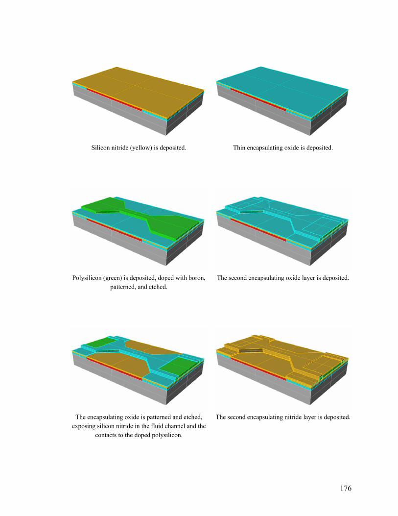
176
Silicon nitride (yellow) is deposited. Thin encapsulating oxide is deposited.
Polysilicon (green) is deposited, doped with boron, patterned, and etched.
The second encapsulating oxide layer is deposited.
The encapsulating oxide is patterned and etched, exposing silicon nitride in the fluid channel and the
contacts to the doped polysilicon.
The second encapsulating nitride layer is deposited.

177
The nitride is patterned with a mask oxide, etched, and the mask oxide stripped.
Aluminum is deposited, patterned, and etched to contact the doped polysilicon, and make traces to
pads at the each of the chip.
The sacrificial polysilicon and bulk silicon are etched by KOH using a thick TEOS mask and the mask is
stripped.