chapter 3 - digital logic level - college of...
TRANSCRIPT

1
Chapter 3 - Digital Logic Level• Gates• Basic Digital Logic• Memory
– Storage Hierarchy• CPU
– PII– PicoJava
• Bus– PCI
• Homework:– Chapter 3 # 1, 4, 6, 12, 25, 35, 37, 40 (Due 4/22)
Chapter 3 - digital logic. We’ll look at gates, basic digital logic, and booleanalgebra. Then we’ll see how these are used to build memory, cpu, and busses -the three core elements of a computer.
Homework: Here is the next

2
Gates and Boolean Algebra
• X = !A;
This is the lowest level we will talk about. You can make gates out of gears,relays, vacuum tubes, tinker toys, transistors, I don’t care.
Lines carry information. In fact, they are boolean variables! They are likevariables in a program. Boxes are operations, like plus, minus, etc.
So, that first picture is just X=!A;
Five basic boolean functions are shown below. All other boolean functions canbe created by compositions of these, just like we can write complex algebraicfunctions x= 3*y2+5
(powers are just repeated multiplications, at least in integerland, which can bebuilt from boolean-land. Computers only approximate reals (at leastnumerically).
“Truth tables” are simply EXTENSIONAL representations of the functions.EXTENSIONAL means listing out all possible combinations of input values,and the corresponding output. This is reasonable because, unlike real or integerdomain functions, boolean functions take a finite set of input values: 2^n,where n is the number of input parameters
(go through not and nand - remember to talk about uninverted output and“inversion” or negation bubbles).
Why is NAND listed before AND? Because, it turns out, in some (most)current realizations, NAND is actually simpler to implement than AND.
Further, NAND and NOR are COMPLETE. That is, ANY boolean functioncan be implemented in terms of either one!
3
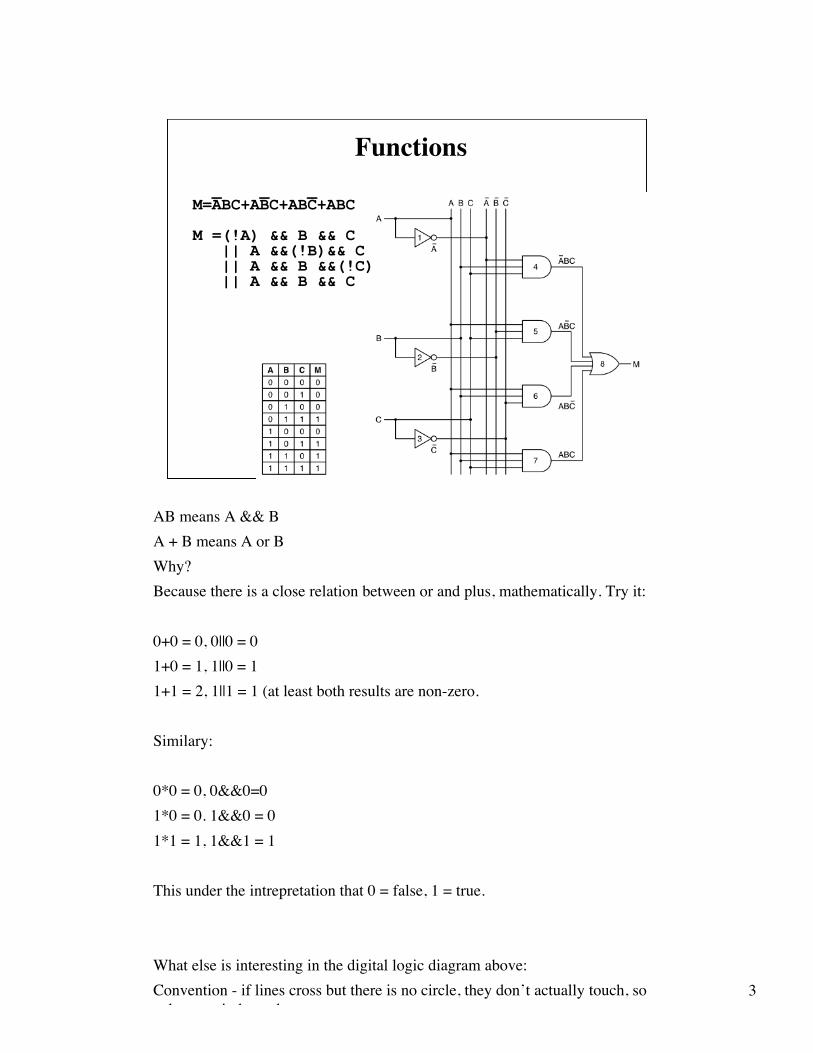
Functions _ _ _M=ABC+ABC+ABC+ABC
M =(!A) && B && C || A &&(!B)&& C || A && B &&(!C) || A && B && C
AB means A && BA + B means A or BWhy?Because there is a close relation between or and plus, mathematically. Try it:
0+0 = 0, 0||0 = 01+0 = 1, 1||0 = 11+1 = 2, 1||1 = 1 (at least both results are non-zero.
Similary:
0*0 = 0, 0&&0=01*0 = 0. 1&&0 = 01*1 = 1, 1&&1 = 1
This under the intrepretation that 0 = false, 1 = true.
What else is interesting in the digital logic diagram above:Convention - if lines cross but there is no circle, they don’t actually touch, sovalues are independentCommon, but not universal.
Convention - the vertical rows are not function inputs, they are just labelledinternal values. The inputs are at the left.
These derive, somewhat abstractly, from physical layout concerns, but anactuall circuit probably wouldn’t be llaid out quite this way.
Why this weird representation? Because it uses two dimensions, it uses moreof our visual processing hardware than a linear set of equations to represent thesame function. It is also easier to map to the physical pc board or chip whentrying to identify (or wire) physical components performing logical functions.
Hmm - so if we can use a 2d graphical rep to advantage at the digital logiclayer, can we use it at higher layers as well? Sure, we do all the time. Think ofsome of the architecture diagrams we’ve seen, think flowcharts and othergraphical representations of programs.
But how come Java, VB, C++, etc are textual instead of graphical, then?Interesting question. Talk to Peggy Burnett.
But, notice it takes a lot more space than the equation at the left. As a result,visual analogs for writing software haven’t really caught on.

4
Completeness of NAND and NOR
Any boolean function can be computed in terms of nand or nor alone!

5
Equivalence and Minimization
• XX+YY = X+Y
These two circuits compute the same function!AB+AC = A(B+C)
Obviously we would like minimal realizations of functions we need, right?
We need some laws for how we can transform functions, so we can search forsimpler forms

6
Identities for formula transform
Here are some laws, stated in two different forms, depending on whether weare working with and gates or with or gates.
Note that, just like in regular algebra, 0 is the additive identity and 1 is themultiplicative identity!
Math is cool!
You should know most of these, except maybe the null law, the Absorptionlaw, and DeMorgan’s law. (Actually, you should know all these from 231 -how many don’t?)
DeMorgan’s law tells you how you can change from an AND gate to an ORgate, or vice-versa.
Also interesting - notice in reasoning about circuits, we switched fromgraphical representation to textual. Interesting.
7
Transforming formulas
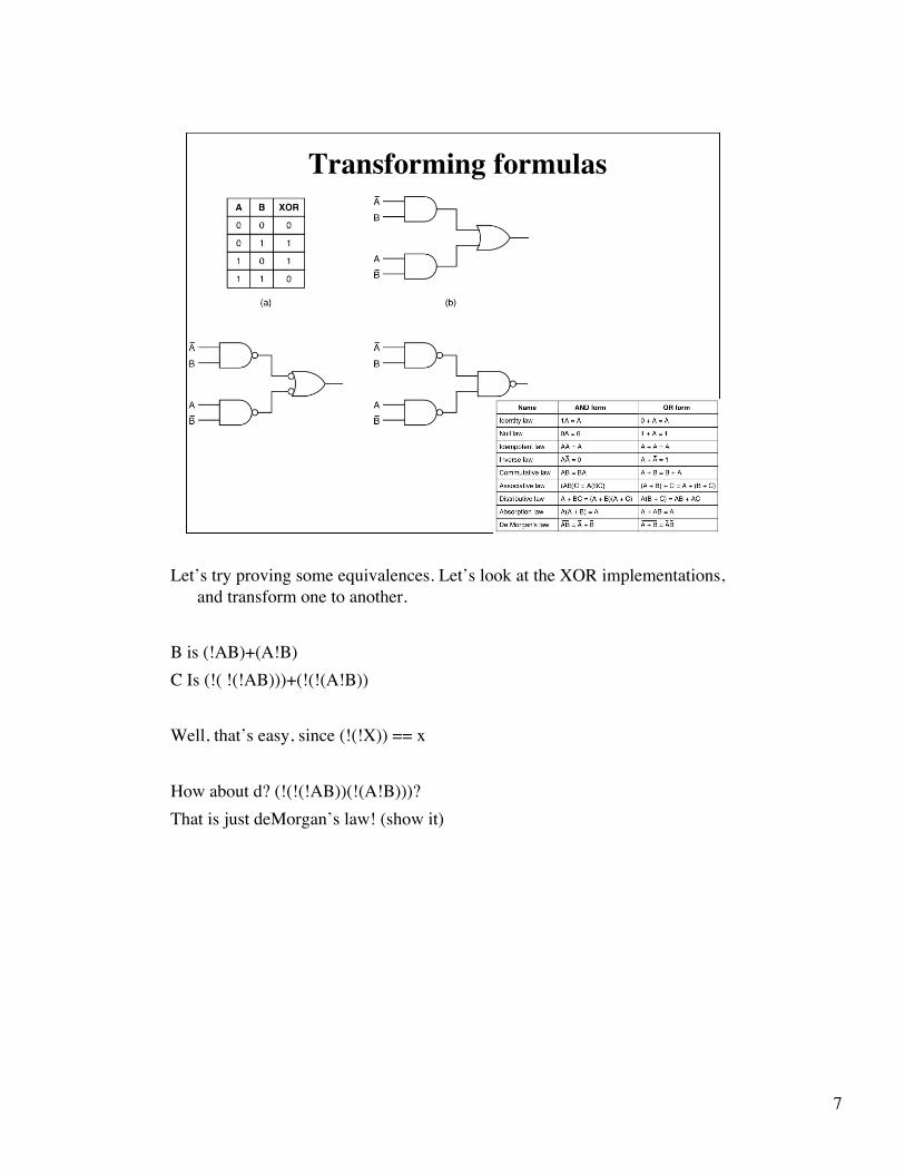
Let’s try proving some equivalences. Let’s look at the XOR implementations,and transform one to another.
B is (!AB)+(A!B)C Is (!( !(!AB)))+(!(!(A!B))
Well, that’s easy, since (!(!X)) == x
How about d? (!(!(!AB))(!(A!B)))?That is just deMorgan’s law! (show it)

8
0-60 in 4.2 sec.
So, we can get from individual gates to a full ALU in just a few steps.
Upper left” simple muliplexer. Last gate is an or. How does this work?
Upper right: full alu: does(1)ALU instruction decode (lower right, converts two bit number into fourseparate control lines, only one of which is on at a time - step throught this!(2) Logic - A and B, A or B, ~B(3) ALU - adds 2 1Bit numbers, with carry in and outDo we need to step through boolean addition? Probably - add two three-bitnumbers, showing carry out of each stage to next state
Bottom shows how 1 bit slices can be combined to create an 8 bit ALU. Whatis “INC” in at right? Usually 0, can be a “1” if our goal is just to increment byone
Huh? Well, that is what “ENA and ENB are for, set ENB to false, and B willlook like all zero. So we can use the same hardware to increment A by 1,without having a separate register to hold the “one”.
Hardware people do that all the time, sigh.

9
Memory
• SR Latch
So far we have looked at combinatorial logic - functions!. Functions aretransformers, but they don’t remember anything!
So how can we build a register?
The SR latch is a simple one-bit memory. How does it work? Let’s try to do atruth table for it:
If S is 1 and R is 0… (S=1 -> !Q = 0 regardless of Q. Therefore inputs to lowergate are both zero, therefore Q is … 1!
Similarly, if S is 0 and R is 1… !Q = 1 and Q = 0
If S is 0 and R is 0… Then there are two stable states, depending on whether Swas 1 or R was 1 last.So with S and R both 0, outputs stay where they are!
How about if S and R are both 1? That forces both Q and !Q to zero. Later,when both S and R go to zero, both nor gates want to output 1. But that willcause the other’s output to go to zero. This is an unstable state, whicheventually (ns) will be resolved by the latch going into one (unpredictablewhich) of its two stable states.
10
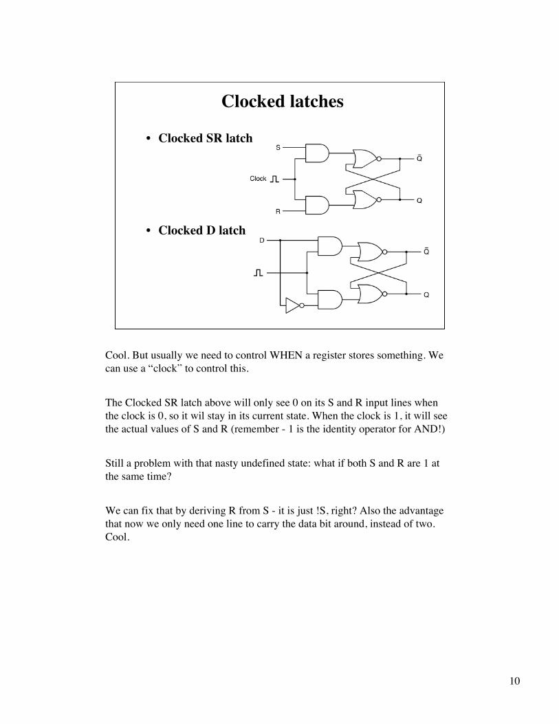
Clocked latches
• Clocked SR latch
• Clocked D latch
Cool. But usually we need to control WHEN a register stores something. Wecan use a “clock” to control this.
The Clocked SR latch above will only see 0 on its S and R input lines whenthe clock is 0, so it wil stay in its current state. When the clock is 1, it will seethe actual values of S and R (remember - 1 is the identity operator for AND!)
Still a problem with that nasty undefined state: what if both S and R are 1 atthe same time?
We can fix that by deriving R from S - it is just !S, right? Also the advantagethat now we only need one line to carry the data bit around, instead of two.Cool.

11
Clocking
One more step to the most common storage: Because of various kinds of noise,including timing skew, it is easier to design such that we guarantee the signalswill be present at a certain place at a particular time in the cycle, rather thanfor an extended duration.
So, a FLIP-FLOP stores data on an EDGE rather than during a duration.EDGE’s can be generated locally, as shown above. We can then use that as theinput to our D latch, generating a D flip-flop
(this is not completely standard notation. I am used to hearing “edge-triggered” vs “level-triggered” to be completely unambiguous).

12
D Flip-Flop
Above is the digital logic diagram for a D flip-flop. It uses our edge generatorto extract an up edge from the clock
Below are some symbols typically used to represent various D latches and flipflops. What is the difference? Note the > and o. What do these mean?
ÿ “>” Means edge triggered.
ÿ “o” has its usual meaning - inversion. So a “o” on the clock input meansthis one stores when the clock value is 0, or, for edge triggered, when the clockis going from 1 to 0.

13
4 x 3 (3?)
Ok, what might a memory look like, then? For example, a register set inside acpu?
Shown above is a 4 x 3 bit register set. Why three bit? Because that is howmany fit on the page in the book!
Notice inconsistency in numbering input and output lines!
We see each bit is stored in a d flip-flop.
We see the three data in lines coming in at the top.
We see three output lines going out at the bottom.What else? We see three control lines:
CS - chip selectRD - readOE - output enable
So, if chip select is true, this block is active (that enables us to combinemultiple chips to make a 8x3 or 12x3 or 16x3 or … using external logic todecode the add’l address lines.
<Explain for 8x3 how this would work>
So, what does cs actually do? Well, first of all let’s decode the D clock inputs.We see that CS+!RD is an input to the “write gates” - in other words, theflip-flops will only see a clock positive when CS is true AND RD is false.
But that is only one of two inputs to the write gate for each row. The otherinput is the adress decode output. Check out the address decode logic atleft: if Ao and A1 are both zero, then the top row sees a 1 on its wordselect line, and all other rows see a zero. So, if we apply A1 = 0, A0 = 1,CS=true, RD=false, THEN the three top gates will see a clock true, andstore the data on the input lines. Note that ALL these must be true for thisto happen.
Similarly for A0=1, A1 =0 (note I tend to use “0/1” when talking about bitsrepresenting integers, like memory addresses, and “true/false” whentalkiing about values that represent logical values, like clock true/false. Forthis course, “true == 1”, “false == 0”, always.
Now let’s look at the output side: if A0=0 and A1=0 then word 0 select linewill be true and all other word select lines will be false.
This means of the four input lines to the lower right or gate, the one from word0 will have the same value as word 0 bit 2, whereas the other three will be0.
So will O1 have the value of Word 0 bit 2?
Well, maybe. What is that last funny symbol? Looks like an inverter withoutthe circle at the end.
Non-inverting buffer. When its “control input” is true, its output is connects toits input. When its “control input” is false, its output is essentiallydisconnected.
Why? So you can(1) Connect a bunch of these together, all connected to the same wires.(2) Connect outputs and inputs together! (Huh?)

14
Simple Bus
Simple? Surely you jest! No really.
We’ll look at buses in more detail shortly, but just to close off the discussionof memory, lets see how some of those features at the memory level translateinto features at the bus level.
First of all, notice the overall bus organization: control, address, and data.
Second, notice the bus data wires are directionless! The memories can bothread and write to the same wires.
But, notice this design can’t transfer from one memory to the other directly,because there is no way to address both at once.
Notice the use of an inverter on the CS of the second ram to use the thurdaddress line as a select for which chip is selected.

15
Dynamic RAM
Dynamic ram uses a different storage mechanism that relies on storing chargein a capacitor.
ROM uses yet a different mechanism for storage.
16
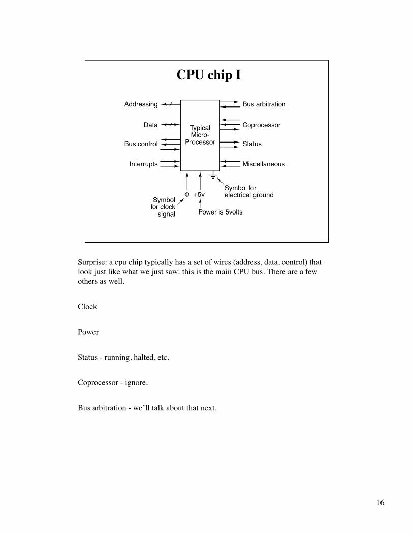
CPU chip I
Surprise: a cpu chip typically has a set of wires (address, data, control) thatlook just like what we just saw: this is the main CPU bus. There are a fewothers as well.
Clock
Power
Status - running, halted, etc.
Coprocessor - ignore.
Bus arbitration - we’ll talk about that next.

17
Buses Everywhere!
We looked at a bus to connect to internal cpu registers, at left.
We also saw the cpu bus, in terms of pins on the cpu chip itself - that is the busconnecting the cpu to the Bus controller.
Above is typical modern layout. The bus “chipset” is the dominant componentyou hear techies talking about when they say “oh, that motherboard has theIntel 8xyz!q###1 chipset!”
So what’s the big deal? Everyone knows about cpu clock, memory size, etc.Don’t hear nuch about busses. Let’s look at Buses
18
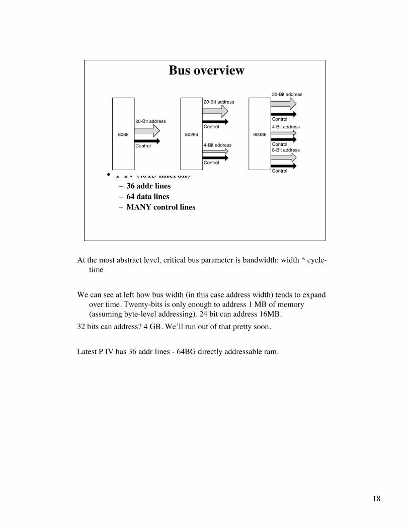
Bus overview
• P IV (.013 micron)– 36 addr lines– 64 data lines– MANY control lines
At the most abstract level, critical bus parameter is bandwidth: width * cycle-time
We can see at left how bus width (in this case address width) tends to expandover time. Twenty-bits is only enough to address 1 MB of memory(assuming byte-level addressing). 24 bit can address 16MB.
32 bits can address? 4 GB. We’ll run out of that pretty soon.
Latest P IV has 36 addr lines - 64BG directly addressable ram.

19
Synchronous bus overview
Ok, so here is a “synchronous” bus.
In a synchronous bus, everything happens to the tune of a master clock (thinkthe old roman slave galleys, with a master drum beater setting the rowingpace. - everyone pulls on the oars when the drum beats.)
Let’s look at a typical simplified synchronous bus: The bus “speed” is thefrequency of the clock. Although that is not necessarily the data rate, as wewill see.
This bus has four control lines: clock, !MREQ, !RD, !WAIT unknown number of address lines - doesn’t really matter for our purposes
here. similarly, unknown number of data lines
Example is a 40 mhz bus - that is, T1 is 25 ns (as is T2, T3, ….)
Here’s the deal: suppose I want to read a memory location. Then I assert!MREQ and !RD simultaneously - that is, since they are both negative, Iset them both to zero (why -in old day made it easy to share).
But note that BEFORE I do that, I have to make sure the address is on theaddress lines (in out example, TML, 6ns, earlier. Why: to give the addressdecode logic in the memory subsystem a chance to stablize!
Then I wait. Usually only one full cycle, then the data is supposed to show up.So this bus can transfer one set of data (however wide the data bus is)every 2 cycles, or one set every 50 ns. In order to do that, it needs memorythat can go from address in to data out in 25 ns! What if memory isn’ tthatfast?
1. Slow down bus.2. Insert “Wait” states - if memory needs more time it can assert “wait” untill
data is available. In the example, wait is asserted for one cycle, meaningentire request took 3 cycles, or 75 ns.
3. Assuming this is an 8 bit data bus, and memory has 2 wait states, what ismax transfer rate of this bus? 25*(2+2) = 100ns/8 bits = 10 MB/sec.
4. Above is a typical question I might ask.

20
Bus arbitration
Sometimes we have more than 1 bus master.
Bus arbitration decides who gets it.Fixed orderPiorities
Top is example of fixed order. If any device requests bus, arbiter grants it. IfI/O device 1 wants it, it takes it and leaves its outgoing line low. Otherwise itpasses the bus grant line value out to next line.
Does this make sense? How might we implement it?
BusGrantOut = BusGrantIn * (!BusRequest_me) (what would that look like indigital logic? Good question!)
21
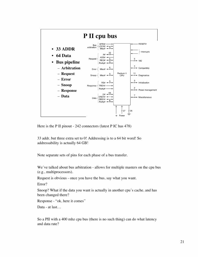
P II cpu bus
• 33 ADDR• 64 Data• Bus pipeline
– Arbitration– Request– Error– Snoop– Response– Data
Here is the P II pinout - 242 connectors (latest P IC has 478)
33 addr, but three extra set to 0! Addressing is to a 64 bit word! Soaddressability is actually 64 GB!
Note separate sets of pins for each phase of a bus transfer.
We’ve talked about bus arbitration - allows for multiple masters on the cpu bus(e.g., multiprocessors).Request is obvious - once you have the bus, say what you want.Error?Snoop? What if the data you want is actually in another cpu’s cache, and hasbeen changed there?Response - “ok, here it comes”Data - at last…
So a PII with a 400 mhz cpu bus (there is no such thing) can do what latencyand data rate?
22
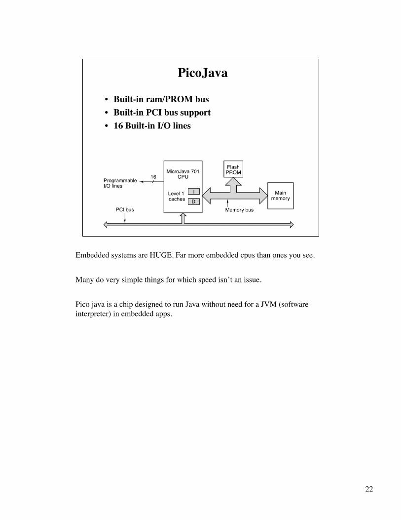
PicoJava
• Built-in ram/PROM bus• Built-in PCI bus support• 16 Built-in I/O lines
Embedded systems are HUGE. Far more embedded cpus than ones you see.
Many do very simple things for which speed isn’t an issue.
Pico java is a chip designed to run Java without need for a JVM (softwareinterpreter) in embedded apps.

23
A real bus - PCI
Overall arch of a motherboard.Of course, these days it gets a bit worse, with AGP II for fast video.Also, these days ISA may be gone completely, and modem, soundcard,ethernet, printe,r all on PCI

24
PCI - more
Several varieties of PCI (voltage, width, clock) we will ignore this, assume3.3V 66 mhz PCI bus
1. Bus is Synchronous2. Bus is MULTIPLEXED! Data and address share same 64 physical lines,
sent one at a time1. Complex bus protocol, sigh.
Centralized arbitration
Basic read and write cycles shown above:
For a read, address put on A/D lines, the lines are turned around, thenresponder puts data on lines.
For a write, turnaround is unnecessary, so write can be done in 3 buscycles, whereas read takes 4.
So, how many bytes/sec can a 66mhz PCI bus transfer in read mode?Write mode?